WO2022185504A1 - マルチバンドフィルタ - Google Patents
マルチバンドフィルタ Download PDFInfo
- Publication number
- WO2022185504A1 WO2022185504A1 PCT/JP2021/008579 JP2021008579W WO2022185504A1 WO 2022185504 A1 WO2022185504 A1 WO 2022185504A1 JP 2021008579 W JP2021008579 W JP 2021008579W WO 2022185504 A1 WO2022185504 A1 WO 2022185504A1
- Authority
- WO
- WIPO (PCT)
- Prior art keywords
- filter
- capacitor
- printed wiring
- wiring board
- inductor
- Prior art date
- Legal status (The legal status is an assumption and is not a legal conclusion. Google has not performed a legal analysis and makes no representation as to the accuracy of the status listed.)
- Ceased
Links
Images








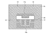




Classifications
-
- H—ELECTRICITY
- H03—ELECTRONIC CIRCUITRY
- H03H—IMPEDANCE NETWORKS, e.g. RESONANT CIRCUITS; RESONATORS
- H03H7/00—Multiple-port networks comprising only passive electrical elements as network components
- H03H7/01—Frequency selective two-port networks
Definitions
- the present disclosure relates to a multiband filter that passes only a plurality of specific frequency bands.
- a multi-band filter has been proposed in which inductors and capacitors are provided for the input/output terminals of filters arranged in parallel.
- a multiband filter can improve attenuation of unwanted signals between passbands of each of a plurality of filters by increasing inductance or capacitance.
- the inductance or capacitance is increased, there is a problem that the matching of the multiband filter is lost, making it difficult to ensure the passbands of each of the plurality of filters.
- This multiband filter includes a first filter, a second filter, inductors, capacitors and transmission lines.
- the first filter and the second filter are arranged in parallel, the inductor is arranged between the first filter and the input/output terminal, and the capacitor is arranged between the input/output terminal and the second filter It is A transmission line is routed between the inductor and the first filter and routed between the capacitor and the second filter.
- the characteristic impedance of the transmission line can be adjusted so that the passbands of the first filter and the second filter do not affect each other.
- the required pass characteristic or attenuation characteristic of the filter is changed and the electrical length of the transmission line is adjusted to be longer, the pass band is narrowed, and the first filter and the second filter.
- the present disclosure solves the above problems, and provides a multi-band filter that can ensure the attenuation of unnecessary signals between the passbands of filters arranged in parallel without affecting each other's passbands. with the aim of obtaining
- the multiband filter includes a printed wiring board, a first input/output terminal and a second input/output terminal provided on the surface of the printed wiring board for inputting and outputting signals, and the surface of the printed wiring board. provided on the surface of the printed wiring board; a first filter provided on the surface of the printed wiring board; , connected to the first input/output terminal by a third transmission line, connected to the second input/output terminal by a fourth transmission line, having a higher frequency passband than the first filter, a second filter arranged in parallel with the filter of; a first inductor, a second inductor, and a third inductor arranged in series with the first transmission line; a fourth inductor, a fifth inductor, and a sixth inductor arranged in series; a first capacitor, a second capacitor, and a third capacitor arranged in series with the third transmission line; A fourth capacitor, a fifth capacitor, and a sixth capacitor arranged in series with the transmission line of each, and one terminal connected to the
- a multi-band filter according to the present disclosure includes a first filter, a second filter arranged in parallel with the first filter, a second capacitor, a third capacitor, a fifth capacitor, a sixth capacitor, a seventh inductor and an eighth inductor.
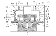
- FIG. 1 is a top view showing the configuration of a multiband filter according to Embodiment 1;
- FIG. 2 is a top view showing the configurations of the multiband filter and the first filter according to Embodiment 1;
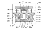
- FIG. 4 is a top view showing the configuration of the first filter in Embodiment 1.
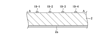
- FIG. FIG. 3 is a cross-sectional arrow diagram showing a cross section of the first filter included in the multiband filter according to Embodiment 1, taken along line AA in FIG. 2;
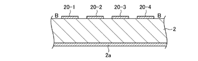
- FIG. 3 is a cross-sectional arrow diagram showing a cross section of the first filter included in the multiband filter according to Embodiment 1, taken along line BB of FIG. 2;
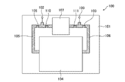
- It is a top view which shows the structure of the conventional multiband filter.
- FIG. 4 is a graph showing pass characteristics of a conventional multiband filter
- 10 is a graph showing pass characteristics of a conventional multiband filter in which the second filter is changed to a wider band filter
- FIG. 10 is a graph showing pass characteristics of a conventional multiband filter in which the second filter is changed to a wider band filter and the conductive pattern of the printed wiring board is adjusted
- FIG. 4 is a graph showing pass characteristics of the multiband filter according to Embodiment 1.
- FIG. 7 is a graph showing pass characteristics of the multiband filter according to Embodiment 1 in which the second filter is changed to a wider band filter;
- FIG. 10 is a top view showing the configuration of Modified Example (1) of the first filter included in the multiband filter according to Embodiment 1;
- FIG. 10 is a top view showing a configuration of a modified example (2) of the first filter included in the multiband filter according to Embodiment 1; 5 is a graph showing pass characteristics of a first filter included in the multiband filter according to Embodiment 1; 7 is a graph showing pass characteristics of the multiband filter according to Embodiment 1 in which the second filter is changed to a wider band filter; 7 is a graph showing pass characteristics of the multiband filter according to Embodiment 1 in which the second filter is changed to a wider band filter, and the element values of inductors and capacitors and the mounting positions of the capacitors are adjusted.
- FIG. 4 is a top view showing a second-layer conductor pattern of a printed wiring board; FIG.
- FIG. 4 is a top view showing a third-layer conductor pattern of a printed wiring board
- FIG. 10 is a top view showing a fourth-layer conductor pattern of a printed wiring board
- FIG. 3 is a cross-sectional arrow view showing a cross-section of the first filter provided on the printed wiring board of the multilayer substrate, taken along line AA of FIG. 2
- FIG. 3 is a cross-sectional arrow view showing a cross section of the first filter provided on the printed wiring board of the multilayer substrate taken along line BB of FIG. 2
- FIG. 10 is a top view showing the configuration of a multiband filter according to Embodiment 2;
- FIG. 10 is a top view showing a conductor pattern on the back surface of a printed wiring board included in a multiband filter according to Embodiment 2;
- FIG. 2 is a top view showing a conductor pattern on the surface of a printed wiring board for mounting;
- FIG. 10 is a top view showing the multiband filter according to the second embodiment mounted on the printed wiring board for mounting;
- FIG. 12 is a top view showing the configuration of a first filter included in the multiband filter according to Embodiment 3;
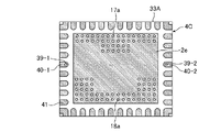
- 27 is a top view showing a conductor pattern on the back surface of the first printed wiring board provided with the first filter of FIG. 26;
- FIG. 27 is a top view showing a conductor pattern on the surface of a second printed wiring board on which the first filter of FIG. 26 is mounted;
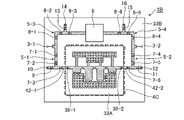
- FIG. 11 is a top view showing the configuration of a multiband filter according to Embodiment 3;
- FIG. 1 is a top view showing the configuration of a multiband filter 1 according to Embodiment 1.
- multiband filter 1 is a two-frequency bandpass filter provided on printed wiring board 2 .
- the printed wiring board 2 is desirably a low-loss substrate such as a fluorine resin substrate.
- the multiband filter 1 includes a first input/output terminal 3-1, a second input/output terminal 3-2, a first filter 4, a first transmission line 5-1, a second transmission line 5-2, Third transmission line 5-3, fourth transmission line 5-4, second filter 6, first inductor 7-1, second inductor 7-2, third inductor 7-3, fourth inductor 7-4, fifth inductor 7-5, sixth inductor 7-6, first capacitor 8-1, second capacitor 8-2, third capacitor 8-3, fourth capacitor 8-4, fifth capacitor 8-5, sixth capacitor 8-6, seventh capacitor 9, via hole 10, eighth capacitor 11, via hole 12, seventh inductor 13, via hole 14, eighth capacitor It has an inductor 15 and a via hole 16 .
- the first input/output terminal 3-1 and the second input/output terminal 3-2 are input/output terminals provided on the surface of the printed wiring board 2 to input/output signals.
- the first filter 4 is provided on the surface of the printed wiring board 2, is connected to the first input/output terminal 3-1 through the first transmission line 5-1, and is connected to the second input/output terminal 3-1 through the second transmission line 5-2. 2 input/output terminal 3-2.
- the second filter 6 is provided on the surface of the printed wiring board 2, is connected to the first input/output terminal 3-1 by the third transmission line 5-3, and is connected to the second input/output terminal 3-1 by the fourth transmission line 5-4. is connected to the input/output terminal 3 - 2 of the first filter 4 , has a higher frequency pass band than the first filter 4 , and is arranged in parallel with the first filter 4 .
- the first inductor 7-1, the second inductor 7-2 and the third inductor 7-3 are arranged in series with the first transmission line 5-1.
- a fourth inductor 7-4, a fifth inductor 7-5 and a sixth inductor 7-6 are arranged in series with the second transmission line 5-2.
- the first capacitor 8-1, the second capacitor 8-2 and the third capacitor 8-3 are arranged in series with the third transmission line 5-3.
- a fourth capacitor 8-4, a fifth capacitor 8-5 and a sixth capacitor 8-6 are arranged in series with the fourth transmission line 5-4.
- the seventh capacitor 9 has one terminal connected to the first transmission line 5-1 between the second inductor 7-2 and the third inductor 7-3, and the other terminal grounded through the via hole 10. It is for example, the via hole 10 electrically connects the ground potential conductor pattern provided on the back surface of the printed wiring board 2 and the seventh capacitor 9 .
- the eighth capacitor 11 has one terminal connected to the second transmission line 5-2 between the fifth inductor 7-5 and the sixth inductor 7-6, and the other terminal grounded through the via hole 12. It is for example, the via hole 12 electrically connects the ground potential conductor pattern provided on the back surface of the printed wiring board 2 and the eighth capacitor 11 .
- the seventh inductor 13 has one terminal connected to the third transmission line 5-3 between the second capacitor 8-2 and the third capacitor 8-3, and the other terminal grounded.
- the via hole 14 electrically connects the ground potential conductor pattern provided on the back surface of the printed wiring board 2 and the seventh inductor 13 .
- the eighth inductor 15 has one terminal connected to the fourth transmission line 5-4 between the fifth capacitor 8-5 and the sixth capacitor 8-6, and the other terminal grounded.
- the via hole 16 electrically connects the ground potential conductor pattern provided on the back surface of the printed wiring board 2 and the eighth inductor 15 .
- FIG. 2 is a top view showing the configuration of the multiband filter 1 and the first filter 4.
- FIG. 3 is a top view showing the configuration of the first filter 4.
- the first filter 4 is a filter provided on the surface of the printed wiring board 2, as shown in FIG.
- the first filter 4 includes a first ground conductor 17, a second ground conductor 18, inductors 19-1 to 19-4 of the distributed constant circuit 21, capacitors 20-1 to 20-4 of the distributed constant circuit 21, capacitors 22-1, 22-2, 24-1 to 24-3, 25-1 to 25-3, 26-1 and 26-2, first resonator 23-1, second resonator 23-2, It has a third resonator 23-3, a fourth resonator 23-4, capacitors 27-1 to 27-3, and input/output terminals 28-1 and 28-2.
- the first ground conductor 17 is provided on the front surface of the printed wiring board 2 and is electrically connected to the ground potential conductor pattern provided on the back surface of the printed wiring board 2 through a plurality of via holes 17a.
- the second ground conductor 18 is provided on the front surface of the printed wiring board 2 and is electrically connected to the ground potential conductor pattern provided on the rear surface of the printed wiring board 2 through a plurality of via holes 18a.
- Inductors 19-1 to 19-4 are provided on the surface of printed wiring board 2, extend from first ground conductor 17 toward second ground conductor 18, and are connected to capacitors 20-1 to 20-4. It is an inductor of the distributed constant circuit 21 provided between the first ground conductor 17 and the second ground conductor 18 .
- the capacitors 20-1 to 20-4 are provided on the surface of the printed wiring board 2 and are conductor patterns formed at the tip portions of the inductors 19-1 to 19-4. It is a capacitor of the distributed constant circuit 21 provided between the ground conductor 18 and the ground conductor 18 .
- the surface mount type capacitors 22-1 and 22-2 are connection capacitors having one terminal connected to the capacitor 20-1 and the other terminal connected to the second ground conductor 18.
- the surface mount type capacitors 24-1 to 24-3 are connection capacitors having one terminal connected to the capacitor 20-2 and the other terminal connected to the second ground conductor 18.
- the surface mount type capacitors 25-1 to 25-3 are connection capacitors having one terminal connected to the capacitor 20-3 and the other terminal connected to the second ground conductor 18.
- the surface mount type capacitors 26-1 and 26-2 are connection capacitors having one terminal connected to the capacitor 20-4 and the other terminal connected to the second ground conductor 18.
- the first resonator 23-1 is a circuit composed of an inductor 19-1, a capacitor 20-1, and capacitors 22-1 and 22-2.
- the second resonator 23-2 is a circuit composed of an inductor 19-2, a capacitor 20-2 and capacitors 24-1 to 24-3.
- the third resonator 23-3 is a circuit composed of an inductor 19-3, a capacitor 20-3 and capacitors 25-1 to 25-3.
- a fourth resonator 23-4 is a circuit composed of an inductor 19-4, a capacitor 20-4, and capacitors 26-1 and 26-2.
- the capacitor 27-1 is a coupling capacitor that couples the capacitor 20-1 of the first resonator 23-1 and the capacitor 20-2 of the second resonator 23-2 adjacent to each other.
- the capacitor 27-2 is a coupling capacitor that couples the capacitor 20-2 of the second resonator 23-2 and the capacitor 20-3 of the third resonator 23-3 adjacent to each other.
- the capacitor 27-3 is a coupling capacitor that couples the capacitor 20-3 of the third resonator 23-3 and the capacitor 20-4 of the fourth resonator 23-4 adjacent to each other.
- the input/output terminal 28-1 is connected to one of the first resonator 23-1, the second resonator 23-2, the third resonator 23-3 and the fourth resonator 23-4. It is an input/output terminal which is provided in the capacitor 20-1 forming one resonator 23-1 and receives and outputs a signal.
- the input/output terminal 28-2 is connected to the other one of the first resonator 23-1, the second resonator 23-2, the third resonator 23-3 and the fourth resonator 23-4. 4, and is an input/output terminal for signal input/output.
- input/output terminal 28-1 is connected to third inductor 7-3.
- the input/output terminal 28-1 is connected to the first input/output terminal 3 via the first transmission line 5-1, the first inductor 7-1, the second inductor 7-2 and the third inductor 7-3. -1.
- input/output terminal 28-2 is connected to sixth inductor 7-6.
- the input/output terminal 28-2 is connected to the second input/output terminal 3 via the second transmission line 5-2, the fourth inductor 7-4, the fifth inductor 7-5 and the sixth inductor 7-6. -2.
- FIG. 4 is a cross-sectional arrow diagram showing a cross section of the first filter 4 provided in the multiband filter 1 taken along line AA in FIG.
- the printed wiring board 2 is a double-sided board and has inductors 19-1 to 19-4 of the distributed constant circuit 21 on its front surface and a ground conductor 2a on its back surface.
- FIG. 5 is a cross-sectional arrow diagram showing a cross-section of the first filter 4 taken along line BB of FIG.
- the capacitors 20-1 to 20-4 of the distributed constant circuit 21 are provided on the surface of the printed wiring board 2, and the ground conductor 2a is provided on the back surface.
- the first ground conductor 17 is electrically connected to the ground conductor 2a provided on the back surface of the printed wiring board 2 through a plurality of via holes 17a.
- the second ground conductor 18 is electrically connected to the ground conductor 2a provided on the back surface of the printed wiring board 2 through a plurality of via holes 18a.
- the ground conductor 2a is a conductor pattern of ground potential.
- FIG. 6 is a top view showing the configuration of a conventional multiband filter 100.
- multiband filter 100 is a conventional two-frequency bandpass filter provided on printed wiring board 101 .
- the multiband filter 100 includes a first input/output terminal 102, a second input/output terminal 103, a first filter 104, a first transmission line 105, a second transmission line 106, a second filter 107, a first inductor 108 , second inductor 109 , first capacitor 110 and second capacitor 111 .
- the first input/output terminal 102 and the second input/output terminal 103 are provided on the surface of the printed wiring board 101 to input/output signals.
- the first filter 104 is provided on the surface of the printed wiring board 101 and connected to the second filter 107 by the first transmission line 105 and the second transmission line 106 .
- a first input/output terminal 102 is connected to the first transmission line 105
- a second input/output terminal 103 is connected to the second transmission line 106 .
- the second filter 107 has a higher frequency passband than the first filter 104 and is arranged in parallel with the first filter 104 .
- the first inductor 108 is arranged in series with the first transmission line 105 between the first input/output terminal 102 and the first filter 104 .
- a second inductor 109 is arranged in series with the second transmission line 106 between the second input/output terminal 103 and the first filter 104 .
- a first capacitor 110 is arranged in series with the first transmission line 105 between the first input/output terminal 102 and the second filter 107 .
- a second capacitor 111 is arranged in series with the second transmission line 106 between the second input/output terminal 103 and the second filter 107 .
- the first inductor 108 and the first capacitor 110, and the second inductor 109 and the second capacitor 111 function as branching circuits or combining circuits.
- the signal component on the low frequency side passes through the first inductor 108, the first filter 104, and the second inductor 109, and passes through the second input/output terminal 102.
- Output from the terminal 103 A signal component on the high frequency side passes through first capacitor 110 , second filter 107 and second capacitor 111 and is output from second input/output terminal 103 .
- Signals outside the passbands of the first filter 104 and the second filter 107 are, for example, reflected at the first input/output terminal 102 and are hardly output from the second input/output terminal 103 .
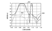
- FIG. 7 is a graph showing pass characteristics of the conventional multiband filter 100.
- a solid line pass characteristic denoted by reference numeral 201 indicates the pass characteristic of the multiband filter 100 .
- the pass characteristic of the dashed line denoted by reference numeral 202 indicates the pass characteristic of the first filter 104 alone.
- a pass characteristic indicated by a one-dot chain line with reference numeral 203 indicates a pass characteristic of the second filter 107 alone.
- the multiband filter 100 has the element values of the first inductor 108, the second inductor 109, the first capacitor 110 and the second capacitor 111, and the values of the first transmission line 105 and the second transmission line 106. If the characteristic impedance and each electrical length are appropriately adjusted, as shown in FIG. attenuation can be ensured.
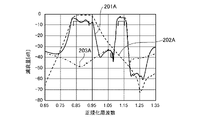
- FIG. 8 is a graph showing pass characteristics of a conventional multiband filter 100 in which the second filter 107 is changed to a wider band filter in order to widen the pass band on the high-frequency side from the pass characteristics of FIG. .
- the solid-line pass characteristic denoted by reference numeral 201A indicates the pass characteristic of the multiband filter 100.
- the pass characteristic of the dashed line denoted by reference numeral 202A indicates the pass characteristic of the first filter 104 alone.
- a transmission characteristic indicated by a one-dot chain line denoted by reference numeral 203A indicates a transmission characteristic of the second filter 107 alone.
- Multiband filter 100 cannot appropriately adjust the characteristic impedances and electrical lengths of first transmission line 105 and second transmission line 106 unless the conductor pattern provided on the surface of printed wiring board 101 is changed. Therefore, even if the second filter 107 is changed to a wider band filter, the pass characteristic of the first filter 104, i. deteriorates.
- FIG. 9 shows a conventional multi-pass filter in which the second filter 107 is changed to a wider band filter and the conductive pattern of the printed wiring board 101 is adjusted in order to widen the pass band on the high frequency side from the pass characteristics of FIG. 4 is a graph showing pass characteristics of the band filter 100;
- a solid line pass characteristic denoted by reference numeral 201B indicates the pass characteristic of the multiband filter 100 .
- the pass characteristic of the dashed line denoted by reference numeral 202B indicates the pass characteristic of the first filter 104 alone.
- a pass characteristic indicated by a one-dot chain line denoted by reference numeral 203B indicates a pass characteristic of the second filter 107 alone.
- multiband filter 100 the conductor pattern provided on the surface of printed wiring board 101 is changed, and each characteristic impedance and each electrical length of first transmission line 105 and second transmission line 106 are appropriately adjusted.
- this suppresses deterioration of the pass characteristic of the first filter 104 on the low-frequency side.
- the pass characteristic of reference numeral 201B the amount of unwanted signal attenuation between the passbands of the first filter 104 and the second filter 107 cannot be ensured.
- the multiband filter 1 when the pass characteristic or the attenuation characteristic is changed, the conductor pattern of the printed wiring board 2 is not changed, and the inductor or Change the element value or mounting position of the capacitor.
- the multiband filter 1 can ensure the amount of unwanted signal attenuation between the passbands of the first filter 4 and the second filter 6 without affecting the passbands of each other.
- the first inductor 7-1 and the first capacitor 8-1 and the fourth inductor 7-4 and the fourth capacitor 8-4 function as a branching circuit or a combining circuit.
- the signal components on the low frequency side are the first inductor 7-1, the second inductor 7-2, the third inductor 7-3, the third 1 filter 4, the sixth inductor 7-6, the fifth inductor 7-5 and the fourth inductor 7-4, and is output from the second input/output terminal 3-2.
- the signal component on the high frequency side is the first capacitor 8-1, the second capacitor 8-2, the third capacitor 8-3, the third 2 filter 6, the sixth capacitor 8-6, the fifth capacitor 8-5 and the fourth capacitor 8-4, and is output from the second input/output terminal 3-2.
- Signals outside the passbands of the first filter 4 and the second filter 6 are, for example, reflected by the first input/output terminal 3-1, and are hardly output from the second input/output terminal 3-2. .
- the multiband filter 1 allows only signals of necessary frequencies to pass through and attenuates unnecessary signals.
- FIG. 10 is a graph showing pass characteristics of the multiband filter 1.
- the solid-line passband denoted by reference numeral 301 is the passband of the multiband filter 1 .
- a pass characteristic indicated by a dashed line denoted by reference numeral 302 indicates a pass characteristic of the first filter 4 alone.
- a transmission characteristic indicated by a one-dot chain line with reference numeral 303 indicates a transmission characteristic of the second filter 6 alone.
- Each element value of the inductor 7-6, the seventh inductor 13 and the eighth inductor 15, the first capacitor 8-1, the second capacitor 8-2, the third capacitor 8-3, the fourth capacitor 8 -4, the fifth capacitor 8-5, the sixth capacitor 8-6, the seventh capacitor 9 and the eighth capacitor 11 are adjusted.
- the multi-band filter 1 is thus able to detect unnecessary noise between the pass bands without affecting the pass characteristics of the first filter 4 and the second filter 6. Signal attenuation can be ensured.
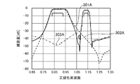
- FIG. 11 is a graph showing pass characteristics of the multiband filter 1 in which the second filter 6 is changed to a wider band filter in order to widen the pass band on the high frequency side from the pass characteristics of FIG.
- the solid-line pass characteristic denoted by reference numeral 301 A is the pass characteristic of the multiband filter 1 .
- a pass characteristic indicated by a dashed line denoted by reference numeral 302A indicates a pass characteristic of the first filter 4 alone.
- a transmission characteristic indicated by a one-dot chain line denoted by reference numeral 303A indicates a transmission characteristic of the second filter 6 alone.
- the multiband filter 1 is thus capable of suppressing unnecessary noise between the respective pass bands without affecting the pass characteristics of the first filter 4 and the second filter 6. Signal attenuation can be ensured.
- a first capacitor 110 and a second capacitor 111 that constitute a branching circuit are arranged in the signal path through which the signal component on the high frequency side propagates in the multiband filter 100. . Therefore, the phase of the signal input/output to/from the second filter 107 is advanced.
- a typical transmission path can retard the phase of a propagating signal, but not advance it.
- the multiband filter 1 includes a second capacitor 8-2, a third capacitor 8-3, a fifth capacitor 8-5, a sixth capacitor 8-6, a seventh inductor 13 and a It has a T-shaped circuit formed by eight inductors 15 .
- the multiband filter 1 can advance the phase of the signal by changing the value of each element in the T-shaped circuit. Attenuation of unnecessary signals between the passbands of the filters 6 can be ensured. Also, there is no need to change the conductor pattern of the printed wiring board 2 .
- FIG. 12 is a top view showing the configuration of a first filter 4A, which is a modified example (1) of the first filter 4.
- FIG. 12 the same components as those in FIG. 3 are given the same reference numerals, and descriptions thereof are omitted.
- the mounting positions of the capacitors 24-1 and 25-1 in the first filter 4 shown in FIG. 3 are assumed to be nominal positions.
- the capacitors 24A-1 and 25A-1 corresponding to these capacitors are shifted from the nominal position to the first ground conductor 17 side (upper side in FIG. 12). It is installed in position.
- FIG. 13 is a top view showing the configuration of a first filter 4B, which is a modified example (2) of the first filter 4.
- FIG. 13 the same components as in FIG. 3 are denoted by the same reference numerals, and descriptions thereof are omitted.
- the mounting positions of the capacitors 24-1 and 25-1 in the first filter 4 shown in FIG. 3 are assumed to be nominal positions.
- the first filter 4B shown in FIG. 13 shifts the capacitors 24B-1 and 25B-1 corresponding to these capacitors to the second ground conductor 18 side (lower side in FIG. 13) from the nominal position. It is installed in the position
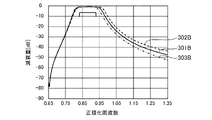
- FIG. 14 is a graph showing pass characteristics of the first filter included in the multiband filter 1.
- the solid-line pass characteristic denoted by reference numeral 301B is the pass characteristic of the first filter 4 having the capacitors 24-1 and 25-1 mounted at nominal positions.
- the pass characteristic indicated by the dashed line labeled 302B is the pass characteristic of the first filter 4A having the capacitors 24A-1 and 25A-1 mounted at positions shifted upward from the nominal position.
- the pass characteristic indicated by a dashed line labeled 303B is the pass characteristic of the first filter 4B having the capacitors 24B-1 and 25B-1 mounted at positions shifted downward from the nominal position.
- the pass characteristics denoted by reference numeral 301B, the pass characteristics denoted by reference numeral 302B, and the pass characteristics denoted by reference numeral 303B not only the capacitance (element value) of the capacitors constituting the T-shaped circuit is changed, but also the The attenuation characteristic of the first filter can also be adjusted by changing the mounting positions of 24-1 and 25-1.
- FIG. 15 is a graph showing pass characteristics of the multiband filter 1 in which the second filter 6 is changed to a wider band filter in order to widen the pass band on the high frequency side from the pass characteristics of FIG.
- the solid-line pass characteristic denoted by reference numeral 301 C indicates the pass characteristic of the multiband filter 1 .
- the pass characteristic of the dashed line denoted by reference numeral 302C indicates the pass characteristic of the first filter 4 alone.
- a transmission characteristic indicated by a one-dot chain line denoted by reference numeral 303C indicates a transmission characteristic of the second filter 6 alone.
- the attenuation in the suppression band (band other than the pass band) of the first filter 4 is insufficient.
- the second filter 6 is changed to a filter with a wider band, the difference in the amount of attenuation in the suppression band between the first filter 4 and the second filter 6 increases, canceling out the mutual attenuation effects. It becomes difficult to secure the amount of attenuation by Therefore, even if each element value in the T-shaped circuit is adjusted, sufficient attenuation of unwanted signals between the passband of the first filter 4 and the passband of the second filter 6 cannot be ensured.
- the second filter 6 is changed to a wider band filter in order to widen the pass band on the high frequency side from the pass characteristics of FIG. 4 is a graph showing pass characteristics of the multiband filter 1 with each element value and mounting position adjusted.
- the solid-line pass characteristic denoted by reference numeral 301D indicates the pass characteristic of the multiband filter 1.
- the pass characteristic of the dashed line denoted by reference numeral 302D indicates the pass characteristic of the first filter 4 alone.
- a transmission characteristic indicated by a one-dot chain line denoted by reference numeral 303D indicates a transmission characteristic of the second filter 6 alone.
- the first inductor 7-1, the second inductor 7-2, the third inductor 7-3, fourth inductor 7-4, fifth inductor 7-5, sixth inductor 7-6, first capacitor 8-1, second capacitor 8-2, third capacitor 8-3, the fourth capacitor 8-4, the fifth capacitor 8-5 and the sixth capacitor 8-6 are adjusted. Furthermore, each of capacitor 22-1, capacitor 22-2, capacitors 24-1 to 24-3, capacitors 25-1 to 25-3, capacitor 26-1 and capacitor 26-2 that constitute first filter 4 Element values or mounting positions are adjusted.
- the printed wiring board 2 may be a multi-layer board having three or more ground conductor layers.
- the printed wiring board 2 is a four-layer board having four layers of ground conductors will be described.
- FIG. 17 is a top view showing a second-layer conductor pattern of the printed wiring board 2 provided in the multiband filter 1 when the printed wiring board 2 is a multi-layer board. As shown in FIG. 17, the second layer of the printed wiring board 2 is provided with a ground conductor 2b.
- the ground conductor 2b is electrically connected to the ground conductors of each layer in the printed wiring board 2 through via holes 10, 12, 14 and 16 and a plurality of via holes 17a and 18a.
- Inductors 19-1 to 19-4 and capacitors 20-1 to 20- of the distributed constant circuit provided on the surface (first layer) of the printed wiring board 2 in the ground conductor 2b of the second layer of the printed wiring board 2 4 is projected downward (second layer), as shown in FIG. 17, the ground conductor 2b is not provided.
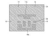
- FIG. 18 is a top view showing the third-layer conductor pattern of the printed wiring board 2.
- the third layer of the printed wiring board 2 is provided with a ground conductor 2c.
- Ground conductor 2c is electrically connected to the ground conductors of each layer in printed wiring board 2 through via holes 10, 12, 14 and 16 and a plurality of via holes 17a and 18a.
- the ground conductor 2c is electrically connected to the fourth-layer ground conductor 2d through a plurality of via holes 29. As shown in FIG.
- the inductors 19-1 to 19-4 of the distributed constant circuit provided on the surface (first layer) of the printed wiring board 2 are arranged downward (third layer). As shown in FIG. 18, no ground conductor 2c is provided in the projected area. Further, in the ground conductor 2c of the third layer of the printed wiring board 2, the capacitors 20-1 to 20-4 of the distributed constant circuit provided on the surface (first layer) of the printed wiring board 2 are placed downward (third layer ) is provided with a ground conductor 2c as shown in FIG. That is, the ground conductor in the inner layer of the printed wiring board 2 is arranged in the area where the capacitors 20-1 to 20-4 of the distributed constant circuit are projected downward.
- FIG. 19 is a top view showing the fourth-layer conductor pattern of the printed wiring board 2, showing the conductor pattern on the back side of the printed wiring board 2 as viewed from the front side.
- the fourth layer of the printed wiring board 2 is provided with a ground conductor 2d over the entire surface.
- Ground conductor 2d is electrically connected to the ground conductors of each layer in printed wiring board 2 through via holes 10, 12, 14 and 16 and a plurality of via holes 17a and 18a.
- the ground conductor 2d is electrically connected to the third-layer ground conductor 2c through a plurality of via holes 29. As shown in FIG.
- the inductors 19-1 to 19-4 of the distributed constant circuit provided on the surface (first layer) of the printed wiring board 2 are arranged downward (fourth layer).
- a ground conductor 2d is provided in the projected area. That is, only the ground conductor 2d on the back surface of the printed wiring board 2 is arranged in the area where the inductors 19-1 to 19-4 of the distributed constant circuit are projected downward.
- FIG. 20 is a cross-sectional arrow diagram showing a cross-section of the first filter 4 provided on the printed wiring board 2, which is a multilayer substrate, taken at the same location as the AA line in FIG.
- the inner layers of the printed wiring board 2 (second and third layers) are provided. ) is not arranged, and only the ground conductor 2d on the back surface (fourth layer) of the printed wiring board 2 is arranged.
- FIG. 21 is a cross-sectional arrow diagram showing a cross-section of the first filter 4 provided on the printed wiring board 2, which is a multi-layer substrate, taken along line BB in FIG.
- a ground conductor 2c on the third layer of the printed wiring board 2 and A fourth-layer ground conductor 2d is arranged below the capacitors 20-1 to 20-4 of the distributed constant circuit provided on the first layer of the printed wiring board 2, a ground conductor 2c on the third layer of the printed wiring board 2 and A fourth-layer ground conductor 2d is arranged.
- the ground conductor 2c is electrically connected to the ground conductor 2d through a plurality of via holes 29. As shown in FIG.
- the multiband filter 1 includes the first filter 4, the second filter 6 arranged in parallel with the first filter 4, and the second capacitor 8- 2, a T-shaped circuit composed of a third capacitor 8-3, a fifth capacitor 8-5, a sixth capacitor 8-6, a seventh inductor 13 and an eighth inductor 15; Even if the required specifications of the filter are changed and the band to be masked is changed, the multiband filter 1 can change the conductor pattern of the printed wiring board 2 by changing the value of each element constituting the T-shaped circuit. Attenuation in the passband or suppression band can be adjusted without modification. As a result, the multiband filter 1 does not affect the passbands of the first filter 4 and the second filter 6, and can ensure the attenuation of unwanted signals between the respective passbands.
- the first filter 4 is provided on the surface of the printed wiring board 2, and is provided on the surface of the printed wiring board 2 with the grounded first ground conductor 17, A grounded second ground conductor 18, inductors 19-1 to 19-4 and capacitors 20-1 to 20 of a distributed constant circuit provided between the first ground conductor 17 and the second ground conductor 18 -4, and connecting capacitors 22-1, 22-2, 24-1 to 24 each having one terminal connected to the capacitors 20-1 to 20-4 and the other terminal connected to the second ground conductor 18. -3, 25-1 to 25-3, 26-1 and 26-2, and adjacent ones are coupled to each other by coupling capacitors 27-1 to 27-3.
- the multiband filter 1 can adjust the frequency characteristics of the filter using a distributed constant circuit that is expected to have a high Q value.
- a capacitor with a low capacitance and expected to have a high Q value can be used, and the loss of the first filter 4 can be reduced.
- printed wiring board 2 may be a multi-layer board having three or more layers of ground conductors electrically connected to each other.
- the printed wiring board 2 Only the ground conductor 2d on the back surface of the wiring board 2 is arranged.
- a ground conductor 2c in the inner layer of the printed wiring board 2 is arranged in a region where the capacitors 20-1 to 20-4 of the distributed constant circuit provided on the first layer of the printed wiring board 2 are projected downward.
- the ground capacitance of the capacitors 20-1 to 20-4 of the distributed constant circuit increases with the same area. can be done. Further, a high Q value can be expected by arranging only the ground conductor 2d on the back surface in the area where the inductors 19-1 to 19-4 of the distributed constant circuit are projected downward. Thereby, it is possible to reduce the size of the first filter 4 while reducing the loss of the filter provided on the surface of the printed wiring board 2 .
- FIG. 22 is a top view showing the configuration of a multiband filter 1A according to Embodiment 2.
- the multiband filter 1A is a two-frequency bandpass filter provided on the surface of the printed wiring board 2A.
- the printed wiring board 2A is a double-sided board in which conductor patterns are formed on the front and back surfaces.
- the printed wiring board according to Embodiment 2 may be a multilayer board.
- the printed wiring board 2A for example, a low-loss printed wiring board for high frequencies is used.
- the multiband filter 1A has an input/output terminal corresponding to the first input/output terminal 3-1 shown in FIG. 2, and a via hole 30-1 is provided at the tip of the input/output terminal.
- the multiband filter 1A also has an input/output terminal corresponding to the second input/output terminal 3-2 shown in FIG. 2, and a via hole 30-2 is provided at the tip of the input/output terminal.
- the first filter 4 may be the first filter 4A or 4B described in the first embodiment.
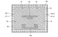
- FIG. 23 is a top view showing the conductor pattern on the back surface of the printed wiring board 2A, showing the conductor pattern on the back surface of the printed wiring board 2A viewed from the front surface side.
- the back surface of the printed wiring board 2A is provided with a ground conductor 2e over the entire surface except for the peripheral portion.
- Ground conductor 2e is electrically connected to the ground conductor on the surface of printed wiring board 2A through via holes 10, 12, 14 and 16 and a plurality of via holes 17a and 18a.
- a conductor pattern 31-1, a conductor pattern 31-2, and a plurality of conductor patterns 32 are provided on the periphery of the back surface of the printed wiring board 2A.
- Conductive pattern 31-1 is a first connection terminal electrically connected to an input/output terminal corresponding to first input/output terminal 3-1 through via hole 30-1.
- the conductor pattern 31-2 is a second connection terminal electrically connected to the input/output terminal corresponding to the second input/output terminal 3-2 through the via hole 30-2.
- FIG. 24 is a top view showing a conductor pattern on the surface of the printed wiring board 33 for mounting.
- the mounting printed wiring board 33 is a mounting printed wiring board provided separately from the printed wiring board 2A, and the printed wiring board 2A is mounted on the surface thereof.
- a ground conductor 2f is provided on the entire surface of the printed wiring board 33 for mounting, excluding the periphery of the mounting area.
- a first input/output terminal 34-1, a second input/output terminal 34-2, a conductor pattern 35-1, a conductor pattern 35-2, and a , a plurality of conductor patterns 36 are provided.
- the first input/output terminal 34-1 is connected to the conductor pattern 35-1, and the second input/output terminal 34-2 is connected to the conductor pattern 35-2.
- a plurality of conductor patterns 36 are provided around the ground conductor 2f.
- the plurality of conductor patterns 36 are arranged so as to surround the printed wiring board 2A in a state in which the printed wiring board 2A provided with the multiband filter 1A is arranged in the mounting area of the mounting printed wiring board 33. .
- a ground conductor is formed on the entire back surface of the mounting printed wiring board 33 .
- Each of the plurality of conductor patterns 36 is electrically connected to the ground conductor on the back surface of the mounting printed wiring board 33 through via holes 37 .
- the ground conductor 2 f is electrically connected to the ground conductor on the back surface of the mounting printed wiring board 33 through a plurality of via holes 38 .
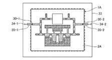
- FIG. 25 is a top view showing the multiband filter 1A mounted on the printed wiring board 33 for mounting.
- a ground conductor 2e and a ground conductor 2f, a conductor pattern 31-1 and a conductor pattern 35-1, a conductor pattern 31-2 and a conductor pattern 35-2, a plurality of conductor patterns 32 and a plurality of conductor patterns 36 are electrically connected to each other by soldering, so that the printed wiring board 2A is surface-mounted on the mounting area of the mounting printed wiring board 33 .
- the first inductor 7-1 and the first capacitor 8-1 and the fourth inductor 7-4 and the fourth capacitor 8-4 function as a branching circuit or a combining circuit.
- the signal component on the low frequency side is the conductor pattern 35-1, the via hole 30-1, the first inductor 7-1, the second inductor 7-. 2, third inductor 7-3, first filter 4, sixth inductor 7-6, fifth inductor 7-5, fourth inductor 7-4, via hole 30-2 and conductor pattern 35-2 and output from the second input/output terminal 34-2.
- the signal component on the high frequency side is the conductor pattern 35-1, the via hole 30-1, the first capacitor 8-1, the second capacitor 8-. 2, third capacitor 8-3, second filter 6, sixth capacitor 8-6, fifth capacitor 8-5, fourth capacitor 8-4, via hole 30-2 and conductor pattern 35-2 and output from the second input/output terminal 34-2.
- Signals outside the passbands of the first filter 4 and the second filter 6 are reflected at the first input/output terminal 34-1 and are hardly output from the second input/output terminal 34-2.
- the multiband filter 1A allows only the signal of the required frequency to pass, and attenuates the unwanted signal.
- the multiband filter 1A includes the conductor pattern 31-1 provided on the back surface of the printed wiring board 2A and electrically connected to the first input/output terminal 3-1. , a conductor pattern 31-2 provided on the rear surface of the printed wiring board 2A and electrically connected to the second input/output terminal 3-2.
- the multiband filter 1A is surface-mounted on the printed wiring board 33 for mounting.
- the multiband filter 1A can obtain effects similar to those of the first and second embodiments. Also, by using a low-loss, expensive printed wiring board as the printed wiring board 2A and using a general-purpose inexpensive printed wiring board as the mounting printed wiring board 33, the cost of the multiband filter 1A can be reduced. be able to.
- FIG. 26 is a top view showing the configuration of the first filter 4C included in the multiband filter 1B according to Embodiment 3.
- FIG. FIG. 27 is a top view showing the conductor pattern on the back surface of the first printed wiring board 33A provided with the first filter 4C, showing the conductor pattern on the back surface of the first printed wiring board 33A as seen from the front surface side.
- FIG. 28 is a top view showing the conductor pattern on the surface of the second printed wiring board 33B.
- FIG. 29 is a top view showing the configuration of the multiband filter 1B. 26, 27, 28 and 29, the same components as those in FIGS. 2 and 3 are denoted by the same reference numerals, and descriptions thereof are omitted.
- the first printed wiring board 33A and the second printed wiring board 33B are double-sided boards, at least one of these printed wiring boards may be a multilayer board.
- the first filter 4C is provided on the surface of the first printed wiring board 33A, as shown in FIG. Since the first filter 4C is provided on the first printed wiring board 33A, for example, a low-loss printed wiring board for high frequencies is used.
- the basic configuration of the conductor pattern forming the first filter 4C is the same as that of the first filter 4 shown in FIG.
- the capacitor 20 of the fourth resonator 23-4 has a conductor pattern extending from the capacitor 20-1 of the resonator 23-1 and having a via hole 39-1 formed at the tip thereof, and corresponding to the input/output terminal 28-2. -4 in that it has a conductor pattern with a via hole 39-2 formed at its tip.
- the first filter 4C is a filter in which the capacitors 24-1 and 25-1 are mounted at positions shifted from the nominal positions, like the first filters 4A and 4B shown in the first embodiment. may
- a ground conductor 2e is provided on the entire surface except for the peripheral edge of the board.
- the ground conductor 2e is electrically connected to a first ground conductor 17 and a second ground conductor 18 provided on the surface of the first printed wiring board 33A through a plurality of via holes 17a and 18a.
- a conductor pattern 40-1, a conductor pattern 40-2 and a plurality of conductor patterns 41 are provided on the periphery of the back surface of the first printed wiring board 33A.
- Conductive pattern 40-1 is a first connection terminal electrically connected to a conductive pattern extending from capacitor 20-1 provided on the surface of first printed wiring board 33A through via hole 39-1.
- the conductor pattern 40-2 is a second connection terminal electrically connected to the conductor pattern extending from the capacitor 20-4 provided on the surface of the first printed wiring board 33A through the via hole 39-2.
- a plurality of conductor patterns 41 are arranged around the ground conductor 2e.
- the second printed wiring board 33B is mounted with the first printed wiring board 33A on which the first filter 4C is mounted.
- a general printed wiring board represented by FR4 is used for the second printed wiring board 33B.
- the second filter 6 provided on the surface of the second printed wiring board 33B is a filter having a higher frequency passband than the first filter 4C.
- a ground conductor 2f is provided on the entire surface of the area of the second printed wiring board 33B excluding the periphery of the mounting area of the first filter 4C.
- a conductor pattern 42-1, a conductor pattern 42-2 and a plurality of conductor patterns 43 are provided on the periphery of the mounting area.
- the conductor pattern 42-1 is a third connection terminal connected to the third inductor 7-3 provided on the surface of the second printed wiring board 33B.
- the conductor pattern 42-2 is a fourth connection terminal connected to the sixth inductor 7-6 provided on the surface of the second printed wiring board 33B.
- a plurality of conductor patterns 43 are provided around the ground conductor 2f.
- the plurality of conductor patterns 43 are arranged in the mounting area of the second printed wiring board 33B while the first printed wiring board 33A provided with the first filter 4C is arranged in the mounting area of the second printed wiring board 33B. It is arranged so as to surround the plate 33A.
- a ground conductor is formed on the entire back surface of the second printed wiring board 33B.
- Each of the plurality of conductor patterns 43 is electrically connected to the ground conductor on the back surface of the second printed wiring board 33B through via holes 44 .
- the ground conductor 2f is electrically connected to the ground conductor on the back surface of the second printed wiring board 33B through a plurality of via holes 45. As shown in FIG.
- the first printed wiring board 33A and the second printed wiring board 33B are, as shown in FIG. By electrically connecting the conductor pattern 42-2, the plurality of conductor patterns 41, and the plurality of conductor patterns 43 with solder, the first printed wiring board 33A is mounted on the second printed wiring board 33B. Area surface mounted.
- the first inductor 7-1 and the first capacitor 8-1 and the fourth inductor 7-4 and the fourth capacitor 8-4 function as a branching circuit or a combining circuit.
- the signal components on the low frequency side are the first inductor 7-1, the second inductor 7-2, the third inductor 7-3, the conductor Pattern 42-1, via hole 39-1, first filter 4, via hole 39-2, conductor pattern 42-2, sixth inductor 7-6, fifth inductor 7-5 and fourth inductor 7-4 and output from the second input/output terminal 3-2.
- the signal component on the high frequency side is the first capacitor 8-1, the second capacitor 8-2, the third capacitor 8-3, the third 2 filter 6, the sixth capacitor 8-6, the fifth capacitor 8-5 and the fourth capacitor 8-4, and is output from the second input/output terminal 3-2.
- Signals outside the passbands of the first filter 4 and the second filter 6 are reflected at the first input/output terminal 3-1 and are hardly output from the second input/output terminal 3-2.
- the multi-band filter 1B allows only signals of necessary frequencies to pass through and attenuates unwanted signals.
- the first printed wiring board 33A may be a multilayer board having three or more layers of ground conductors.
- the inductors 19-1 to 19-4 of the distributed constant circuit included in the first filter 4C provided on the first printed wiring board 33A are arranged downward. Only the ground conductor on the back surface of the first printed wiring board 33A is arranged in the projected area. Furthermore, a ground conductor in the inner layer of the first printed wiring board 33A is arranged in a region where the capacitors 20-1 to 20-4 of the distributed constant circuit provided in the first filter 4C are projected downward.
- the ground capacitance of the capacitors 20-1 to 20-4 of the distributed constant circuit increases with the same area, so the areas of the capacitors 20-1 to 20-4 can be reduced. Further, a high Q value can be expected by arranging only the ground conductor on the back surface in the area where the inductors 19-1 to 19-4 of the distributed constant circuit are projected downward. Thereby, the size of the first filter 4C can be reduced while reducing the loss.
- the multiband filter 1B according to the third embodiment includes the first printed wiring board 33A on which the first filter 4C is mounted, the second filter 6 on which the second filter 6 and other conductor patterns are provided. Two printed wiring boards 33B are provided, and the first printed wiring board 33A is mounted on the second printed wiring board 33B.
- the multiband filter 1B can obtain effects similar to those of the first and second embodiments.
- the second printed wiring board 33B can be provided with an inexpensive A printed wiring board can be used.
- the multiband filter 1B can reduce the size of an expensive printed wiring board, and can be made at a lower cost than the multiband filter 1A according to the second embodiment.
- a multiband filter according to the present disclosure can be used, for example, in a high-frequency device mounted on a communication device.
- 1, 1A, 1B multiband filter 2, 2A printed wiring board, 2a to 2f ground conductor, 3-1, 34-1 first input/output terminal, 3-2, 34-2 second input/output terminal, 4, 4A to 4C first filter, 5-1 first transmission line, 5-2 second transmission line, 5-3 third transmission line, 5-4 fourth transmission line, 6 second filter, 7-1 first inductor, 7-2 second inductor, 7-3 third inductor, 7-4 fourth inductor, 7-5 fifth inductor, 7-6 sixth inductor, 8-1 1st capacitor, 8-2 2nd capacitor, 8-3 3rd capacitor, 8-4 4th capacitor, 8-5 5th capacitor, 8-6 6th capacitor, 9th 7 capacitors, 10, 12, 14, 16, 17a, 18a, 29, 30-1, 30-2, 37, 38, 39-1, 39-2, 44, 45 via holes, 11 8th capacitor, 13 seventh inductor, 15 eighth inductor, 17 first ground conductor, 18 second ground conductor, 19-1 to 19-4 inductors, 20-1 to 20-4, 22-1, 22-2, 24-
Landscapes
- Filters And Equalizers (AREA)
Abstract
マルチバンドフィルタ(1)は、第1のフィルタ(4)と、第1のフィルタ(4)と並列に配置された第2のフィルタ(6)を備え、第1のフィルタ(4)が、接地された第1の地導体(17)と、接地された第2の地導体(18)と、第1の地導体(17)と第2の地導体(18)との間に設けられた分布定数回路(21)のインダクタ(19-1~19-4)およびコンデンサ(20-1~20-4)と、一方の端子がコンデンサ(20-1~20-4)と接続され他方の端子が第2の地導体(18)と接続された接続用コンデンサ(22-1,22-2,24-1~24-3,25-1~25-3,26-1,26-2)によって構成され、結合用コンデンサ(27-1~27-3)によって隣同士が互いに結合された第1の共振器(23-1)、第2の共振器(23-2)、第3の共振器(23-3)および第4の共振器(23-4)を有する。
Description
本開示は、複数の特定周波数帯域のみを通過させるマルチバンドフィルタに関する。
マルチバンドフィルタとして、並列に配置されたフィルタの入出力端子に対してインダクタおよびコンデンサを設けたものが提案されている。マルチバンドフィルタは、インダクタンスまたはキャパシタンスを高くすることで、複数のフィルタそれぞれの通過帯域間の不要信号の減衰量を向上させることができる。ただし、インダクタンスまたはキャパシタンスを高くすると、マルチバンドフィルタの整合が崩れて、複数のフィルタそれぞれの通過帯域の確保が困難になるという問題があった。
この問題を解決する従来の技術として、例えば、特許文献1に記載されるマルチバンドフィルタがある。このマルチバンドフィルタは、第1のフィルタ、第2のフィルタ、インダクタ、コンデンサおよび伝送線路を備えている。第1のフィルタと第2のフィルタとは並列に配置され、インダクタは、第1のフィルタと入出力端子との間に配置され、コンデンサは、入出力端子と第2のフィルタとの間に配置されている。伝送線路は、インダクタと第1のフィルタとの間に配線され、コンデンサと第2のフィルタとの間に配線されている。これらの伝送線路の特性インピーダンスまたは電気長を調整することにより、第1のフィルタと第2のフィルタで互いの通過帯域に影響を与えず、かつ第1のフィルタおよび第2のフィルタそれぞれの通過帯域間の不要信号の減衰量が確保される。
特許文献1に記載されたマルチバンドフィルタでは、第1のフィルタと第2のフィルタで互いの通過帯域が影響を与えないように、伝送線路の特性インピーダンスを調整することはできる。しかしながら、要求されるフィルタの通過特性または減衰特性が変更されることで、伝送線路の電気長が長く調整された場合、通過帯域が狭帯域化することにより、第1のフィルタおよび第2のフィルタのそれぞれの通過帯域間の不要信号の減衰量を十分に確保できないという課題があった。
本開示は上記課題を解決するものであり、並列に配置されたフィルタの互いの通過帯域に影響を与えずにそれぞれの通過帯域間の不要信号の減衰量を確保することができるマルチバンドフィルタを得ることを目的とする。
本開示に係るマルチバンドフィルタは、プリント配線板と、プリント配線板の表面に設けられて、信号が入出力される第1の入出力端子および第2の入出力端子と、プリント配線板の表面に設けられ、第1の伝送線路によって第1の入出力端子と接続され、第2の伝送線路によって第2の入出力端子と接続された第1のフィルタと、プリント配線板の表面に設けられ、第3の伝送線路によって第1の入出力端子と接続され、第4の伝送線路によって第2の入出力端子と接続され、第1のフィルタよりも高い周波数の通過帯域を有し、第1のフィルタと並列に配置された第2のフィルタと、第1の伝送線路にそれぞれ直列に配置された第1のインダクタ、第2のインダクタおよび第3のインダクタと、第2の伝送線路にそれぞれ直列に配置された第4のインダクタ、第5のインダクタおよび第6のインダクタと、第3の伝送線路にそれぞれ直列に配置された第1のコンデンサ、第2のコンデンサおよび第3のコンデンサと、第4の伝送線路にそれぞれ直列に配置された第4のコンデンサ、第5のコンデンサおよび第6のコンデンサと、一方の端子が第2のインダクタと第3のインダクタとの間の第1の伝送線路に接続され、他方の端子が接地された第7のコンデンサと、一方の端子が第5のインダクタと第6のインダクタとの間の第2の伝送線路に接続され、他方の端子が接地された第8のコンデンサと、一方の端子が第2のコンデンサと第3のコンデンサとの間の第3の伝送線路に接続され、他方の端子が接地された第7のインダクタと、一方の端子が第5のコンデンサと第6のコンデンサとの間の第4の伝送線路に接続され、他方の端子が接地された第8のインダクタを備える。
本開示に係るマルチバンドフィルタは、第1のフィルタと、第1のフィルタと並列に配置された第2のフィルタとを備え、第2のコンデンサ、第3のコンデンサ、第5のコンデンサ、第6のコンデンサ、第7のインダクタおよび第8のインダクタによって構成されるT形回路を備える。T形回路を構成する各素子値を変更することで、本開示に係るマルチバンドフィルタは、プリント配線板の導体パターンを変更しなくても、第1のフィルタと第2のフィルタの互いの通過帯域に影響を与えずに、それぞれの通過帯域間の不要信号の減衰量を確保することができる。
実施の形態1.
図1は、実施の形態1に係るマルチバンドフィルタ1の構成を示す上面図である。図1において、マルチバンドフィルタ1は、プリント配線板2に設けられた二周波数帯域通過フィルタである。プリント配線板2は、フッ素樹脂基板などの低損失な基板が望ましい。
マルチバンドフィルタ1は、第1の入出力端子3-1、第2の入出力端子3-2、第1のフィルタ4、第1の伝送線路5-1、第2の伝送線路5-2、第3の伝送線路5-3、第4の伝送線路5-4、第2のフィルタ6、第1のインダクタ7-1、第2のインダクタ7-2、第3のインダクタ7-3、第4のインダクタ7-4、第5のインダクタ7-5、第6のインダクタ7-6、第1のコンデンサ8-1、第2のコンデンサ8-2、第3のコンデンサ8-3、第4のコンデンサ8-4、第5のコンデンサ8-5、第6のコンデンサ8-6、第7のコンデンサ9、ビアホール10、第8のコンデンサ11、ビアホール12、第7のインダクタ13、ビアホール14、第8のインダクタ15およびビアホール16を備える。
図1は、実施の形態1に係るマルチバンドフィルタ1の構成を示す上面図である。図1において、マルチバンドフィルタ1は、プリント配線板2に設けられた二周波数帯域通過フィルタである。プリント配線板2は、フッ素樹脂基板などの低損失な基板が望ましい。
マルチバンドフィルタ1は、第1の入出力端子3-1、第2の入出力端子3-2、第1のフィルタ4、第1の伝送線路5-1、第2の伝送線路5-2、第3の伝送線路5-3、第4の伝送線路5-4、第2のフィルタ6、第1のインダクタ7-1、第2のインダクタ7-2、第3のインダクタ7-3、第4のインダクタ7-4、第5のインダクタ7-5、第6のインダクタ7-6、第1のコンデンサ8-1、第2のコンデンサ8-2、第3のコンデンサ8-3、第4のコンデンサ8-4、第5のコンデンサ8-5、第6のコンデンサ8-6、第7のコンデンサ9、ビアホール10、第8のコンデンサ11、ビアホール12、第7のインダクタ13、ビアホール14、第8のインダクタ15およびビアホール16を備える。
第1の入出力端子3-1および第2の入出力端子3-2は、プリント配線板2の表面に設けられて、信号が入出力される入出力端子である。第1のフィルタ4は、プリント配線板2の表面に設けられて、第1の伝送線路5-1によって第1の入出力端子3-1と接続され、第2の伝送線路5-2によって第2の入出力端子3-2と接続されている。第2のフィルタ6は、プリント配線板2の表面に設けられ、第3の伝送線路5-3によって第1の入出力端子3-1と接続され、第4の伝送線路5-4によって第2の入出力端子3-2と接続され、第1のフィルタ4よりも高い周波数の通過帯域を有し、第1のフィルタ4と並列に配置されている。
第1のインダクタ7-1、第2のインダクタ7-2および第3のインダクタ7-3は、第1の伝送線路5-1にそれぞれ直列に配置されている。第4のインダクタ7-4、第5のインダクタ7-5および第6のインダクタ7-6は、第2の伝送線路5-2にそれぞれ直列に配置されている。第1のコンデンサ8-1、第2のコンデンサ8-2および第3のコンデンサ8-3は、第3の伝送線路5-3にそれぞれ直列に配置されている。さらに、第4のコンデンサ8-4、第5のコンデンサ8-5および第6のコンデンサ8-6は、第4の伝送線路5-4にそれぞれ直列に配置されている。
第7のコンデンサ9は、一方の端子が第2のインダクタ7-2と第3のインダクタ7-3との間の第1の伝送線路5-1に接続され、他方の端子がビアホール10によって接地されている。例えば、ビアホール10は、プリント配線板2の裏面に設けられた接地電位の導体パターンと第7のコンデンサ9とを電気的に接続する。
第8のコンデンサ11は、一方の端子が第5のインダクタ7-5と第6のインダクタ7-6との間の第2の伝送線路5-2に接続され、他方の端子がビアホール12によって接地されている。例えば、ビアホール12は、プリント配線板2の裏面に設けられた接地電位の導体パターンと第8のコンデンサ11とを電気的に接続する。
第7のインダクタ13は、一方の端子が第2のコンデンサ8-2と第3のコンデンサ8-3との間の第3の伝送線路5-3に接続され、他方の端子が接地されている。例えば、ビアホール14は、プリント配線板2の裏面に設けられた接地電位の導体パターンと第7のインダクタ13とを電気的に接続する。
第8のインダクタ15は、一方の端子が第5のコンデンサ8-5と第6のコンデンサ8-6との間の第4の伝送線路5-4に接続され、他方の端子が接地されている。例えば、ビアホール16は、プリント配線板2の裏面に設けられた接地電位の導体パターンと第8のインダクタ15とを電気的に接続する。
第8のインダクタ15は、一方の端子が第5のコンデンサ8-5と第6のコンデンサ8-6との間の第4の伝送線路5-4に接続され、他方の端子が接地されている。例えば、ビアホール16は、プリント配線板2の裏面に設けられた接地電位の導体パターンと第8のインダクタ15とを電気的に接続する。
図2は、マルチバンドフィルタ1および第1のフィルタ4の構成を示す上面図である。図3は、第1のフィルタ4の構成を示す上面図である。第1のフィルタ4は、図3に示すように、プリント配線板2の表面上に設けられたフィルタである。第1のフィルタ4は、第1の地導体17、第2の地導体18、分布定数回路21のインダクタ19-1~19-4、分布定数回路21のコンデンサ20-1~20-4、コンデンサ22-1、22-2、24-1~24-3、25-1~25-3、26-1および26-2、第1の共振器23-1、第2の共振器23-2、第3の共振器23-3、第4の共振器23-4、コンデンサ27-1~27-3、および、入出力端子28-1および28-2を有する。
第1の地導体17は、プリント配線板2の表面に設けられ、複数のビアホール17aによって、プリント配線板2の裏面に設けられた接地電位の導体パターンと電気的に接続されている。第2の地導体18は、プリント配線板2の表面に設けられ、複数のビアホール18aによって、プリント配線板2の裏面に設けられた接地電位の導体パターンと電気的に接続されている。
インダクタ19-1~19-4は、プリント配線板2の表面に設けられ、第1の地導体17から第2の地導体18に向かって延びて、コンデンサ20-1~20-4に接続している導体パターンであり、第1の地導体17と第2の地導体18との間に設けられた分布定数回路21のインダクタである。コンデンサ20-1~20-4は、プリント配線板2の表面に設けられ、インダクタ19-1~19-4の先端部分に形成された導体パターンであり、第1の地導体17と第2の地導体18との間に設けられた分布定数回路21のコンデンサである。
表面実装タイプのコンデンサ22-1および22-2は、一方の端子がコンデンサ20-1と接続され、他方の端子が第2の地導体18と接続された接続用コンデンサである。
表面実装タイプのコンデンサ24-1~24-3は、一方の端子がコンデンサ20-2と接続され、他方の端子が第2の地導体18と接続された接続用コンデンサである。
表面実装タイプのコンデンサ25-1~25-3は、一方の端子がコンデンサ20-3と接続され、他方の端子が第2の地導体18と接続された接続用コンデンサである。
表面実装タイプのコンデンサ26-1および26-2は、一方の端子がコンデンサ20-4と接続され、他方の端子が第2の地導体18と接続された接続用コンデンサである。
表面実装タイプのコンデンサ24-1~24-3は、一方の端子がコンデンサ20-2と接続され、他方の端子が第2の地導体18と接続された接続用コンデンサである。
表面実装タイプのコンデンサ25-1~25-3は、一方の端子がコンデンサ20-3と接続され、他方の端子が第2の地導体18と接続された接続用コンデンサである。
表面実装タイプのコンデンサ26-1および26-2は、一方の端子がコンデンサ20-4と接続され、他方の端子が第2の地導体18と接続された接続用コンデンサである。
第1の共振器23-1は、インダクタ19-1、コンデンサ20-1、および、コンデンサ22-1および22-2によって構成された回路である。第2の共振器23-2は、インダクタ19-2、コンデンサ20-2およびコンデンサ24-1~24-3によって構成された回路である。第3の共振器23-3は、インダクタ19-3、コンデンサ20-3およびコンデンサ25-1~25-3によって構成された回路である。第4の共振器23-4は、インダクタ19-4、コンデンサ20-4、および、コンデンサ26-1および26-2によって構成された回路である。
コンデンサ27-1は、隣同士の第1の共振器23-1のコンデンサ20-1と第2の共振器23-2のコンデンサ20-2とを互いに結合する結合用コンデンサである。
コンデンサ27-2は、隣同士の第2の共振器23-2のコンデンサ20-2と第3の共振器23-3のコンデンサ20-3とを互いに結合する結合用コンデンサである。
コンデンサ27-3は、隣同士の第3の共振器23-3のコンデンサ20-3と第4の共振器23-4のコンデンサ20-4とを互いに結合する結合用コンデンサである。
コンデンサ27-2は、隣同士の第2の共振器23-2のコンデンサ20-2と第3の共振器23-3のコンデンサ20-3とを互いに結合する結合用コンデンサである。
コンデンサ27-3は、隣同士の第3の共振器23-3のコンデンサ20-3と第4の共振器23-4のコンデンサ20-4とを互いに結合する結合用コンデンサである。
入出力端子28-1は、第1の共振器23-1、第2の共振器23-2、第3の共振器23-3および第4の共振器23-4のうち、一方側の第1の共振器23-1を構成するコンデンサ20-1に設けられ、信号が入出力される入出力端子である。
入出力端子28-2は、第1の共振器23-1、第2の共振器23-2、第3の共振器23-3および第4の共振器23-4のうち、他方側の第4の共振器23-4を構成するコンデンサ20-4に設けられ、信号が入出力される入出力端子である。
入出力端子28-2は、第1の共振器23-1、第2の共振器23-2、第3の共振器23-3および第4の共振器23-4のうち、他方側の第4の共振器23-4を構成するコンデンサ20-4に設けられ、信号が入出力される入出力端子である。
図2に示すように、入出力端子28-1は、第3のインダクタ7-3と接続される。入出力端子28-1は、第1の伝送線路5-1、第1のインダクタ7-1、第2のインダクタ7-2および第3のインダクタ7-3を介して第1の入出力端子3-1に接続される。
同様に、入出力端子28-2は、第6のインダクタ7-6と接続される。入出力端子28-2は、第2の伝送線路5-2、第4のインダクタ7-4、第5のインダクタ7-5および第6のインダクタ7-6を介して第2の入出力端子3-2に接続される。
同様に、入出力端子28-2は、第6のインダクタ7-6と接続される。入出力端子28-2は、第2の伝送線路5-2、第4のインダクタ7-4、第5のインダクタ7-5および第6のインダクタ7-6を介して第2の入出力端子3-2に接続される。
図4は、マルチバンドフィルタ1が備える第1のフィルタ4を図2のA-A線で切った断面を示す断面矢示図である。図4に示すように、プリント配線板2は両面基板であり、表面に分布定数回路21のインダクタ19-1~19-4が設けられ、裏面には、地導体2aが設けられている。図5は、第1のフィルタ4を図2のB-B線で切った断面を示す断面矢示図である。図5に示すように、プリント配線板2の表面に分布定数回路21のコンデンサ20-1~20-4が設けられ、裏面には、地導体2aが設けられている。
第1の地導体17は、プリント配線板2の裏面に設けられた地導体2aと電複数のビアホール17aによって気的に接続されている。また、第2の地導体18は、プリント配線板2の裏面に設けられた地導体2aと電複数のビアホール18aによって気的に接続されている。地導体2aは、接地電位の導体パターンである。
実施の形態1に係るマルチバンドフィルタ1と比較するため、従来のマルチバンドフィルタについて説明する。図6は、従来のマルチバンドフィルタ100の構成を示す上面図である。図6において、マルチバンドフィルタ100は、プリント配線板101に設けられた、従来の二周波数帯域通過フィルタである。マルチバンドフィルタ100は、第1の入出力端子102、第2の入出力端子103、第1のフィルタ104、第1の伝送線路105、第2の伝送線路106、第2のフィルタ107、第1のインダクタ108、第2のインダクタ109、第1のコンデンサ110および第2のコンデンサ111を備える。
第1の入出力端子102および第2の入出力端子103は、プリント配線板101の表面に設けられ、信号が入出力される。第1のフィルタ104は、プリント配線板101の表面に設けられ、第1の伝送線路105と第2の伝送線路106によって第2のフィルタ107と接続されている。第1の伝送線路105には、第1の入出力端子102が接続されており、第2の伝送線路106には、第2の入出力端子103が接続されている。第2のフィルタ107は、第1のフィルタ104よりも高い周波数の通過帯域を有し、第1のフィルタ104と並列に配置されている。
第1のインダクタ108は、第1の入出力端子102と第1のフィルタ104との間の第1の伝送線路105に直列に配置されている。第2のインダクタ109は、第2の入出力端子103と第1のフィルタ104との間の第2の伝送線路106に直列に配置されている。第1のコンデンサ110は、第1の入出力端子102と第2のフィルタ107との間の第1の伝送線路105に直列に配置されている。第2のコンデンサ111は、第2の入出力端子103と第2のフィルタ107との間の第2の伝送線路106に直列に配置されている。
マルチバンドフィルタ100において、第1のインダクタ108および第1のコンデンサ110と、第2のインダクタ109および第2のコンデンサ111とが、分波回路または合波回路として機能する。第1の入出力端子102に入力された信号のうち、低域側の信号成分は、第1のインダクタ108、第1のフィルタ104および第2のインダクタ109を通過して、第2の入出力端子103から出力される。高域側の信号成分は、第1のコンデンサ110、第2のフィルタ107および第2のコンデンサ111を通過し、第2の入出力端子103から出力される。第1のフィルタ104および第2のフィルタ107の通過帯域以外の信号は、例えば、第1の入出力端子102で反射することにより、第2の入出力端子103から殆ど出力されない。
図7は、従来のマルチバンドフィルタ100の通過特性を示すグラフである。図7において、符号201を付した実線の通過特性は、マルチバンドフィルタ100の通過特性を示している。また、符号202を付した破線の通過特性は、第1のフィルタ104単体の通過特性を示している。符号203を付した一点鎖線の通過特性は、第2のフィルタ107単体の通過特性を示している。
マルチバンドフィルタ100は、第1のインダクタ108、第2のインダクタ109、第1のコンデンサ110および第2のコンデンサ111の各素子値と、第1の伝送線路105および第2の伝送線路106の各特性インピーダンスおよび各電気長とが適切に調整されれば、図7に示すように、第1のフィルタ104および第2のフィルタ107の互いの通過特性に影響を与えずに、それぞれの通過特性間の減衰量を確保することができる。
図8は、図7の通過特性よりも高域側の通過帯域を広げるために、第2のフィルタ107をより広帯域なフィルタに変更した、従来のマルチバンドフィルタ100の通過特性を示すグラフである。図8において、符号201Aを付した実線の通過特性は、マルチバンドフィルタ100の通過特性を示している。また、符号202Aを付した破線の通過特性は、第1のフィルタ104単体の通過特性を示している。符号203Aを付した一点鎖線の通過特性は、第2のフィルタ107単体の通過特性を示している。
マルチバンドフィルタ100は、プリント配線板101の表面に設けられた導体パターンを変更しない場合、第1の伝送線路105および第2の伝送線路106の各特性インピーダンスおよび各電気長を適切に調整できない。このため、第2のフィルタ107がより広帯域なフィルタに変更された場合であっても、符号201Aの通過特性から明らかなように、第1のフィルタ104における通過特性、すなわち低域側の通過特性が劣化する。
図9は、図7の通過特性よりも高域側の通過帯域を広げるために、第2のフィルタ107をより広帯域なフィルタに変更し、プリント配線板101の導電パターンを調整した、従来のマルチバンドフィルタ100の通過特性を示すグラフである。図9において、符号201Bを付した実線の通過特性は、マルチバンドフィルタ100の通過特性を示している。また、符号202Bを付した破線の通過特性は、第1のフィルタ104単体の通過特性を示している。符号203Bを付した一点鎖線の通過特性は、第2のフィルタ107単体の通過特性を示している。
マルチバンドフィルタ100は、プリント配線板101の表面に設けられた導体パターンが変更されて、第1の伝送線路105および第2の伝送線路106の各特性インピーダンスおよび各電気長が適切に調整されている。これにより、符号201Bの通過特性から明らかなように、第1のフィルタ104における低域側の通過特性の劣化が抑えられる。しかしながら、符号201Bの通過特性においては、第1のフィルタ104および第2のフィルタ107のそれぞれの通過帯域間の不要信号の減衰量が確保できていない。
これに対して、実施の形態1に係るマルチバンドフィルタ1は、通過特性または減衰特性が変更された場合、プリント配線板2の導体パターンを変更せず、第1のフィルタ4を構成するインダクタまたはコンデンサの素子値または搭載位置を変更する。これにより、マルチバンドフィルタ1は、第1のフィルタ4および第2のフィルタ6の互いの通過帯域に影響を与えずに、それぞれの通過帯域間の不要信号の減衰量を確保することができる。
マルチバンドフィルタ1において、第1のインダクタ7-1および第1のコンデンサ8-1と第4のインダクタ7-4および第4のコンデンサ8-4とが、分波回路または合波回路として機能する。第1の入出力端子3-1に入力された信号のうち、低域側の信号成分は、第1のインダクタ7-1、第2のインダクタ7-2、第3のインダクタ7-3、第1のフィルタ4、第6のインダクタ7-6、第5のインダクタ7-5および第4のインダクタ7-4を通過して、第2の入出力端子3-2から出力される。
第1の入出力端子3-1に入力された信号のうち、高域側の信号成分は、第1のコンデンサ8-1、第2のコンデンサ8-2、第3のコンデンサ8-3、第2のフィルタ6、第6のコンデンサ8-6、第5のコンデンサ8-5および第4のコンデンサ8-4を通過して、第2の入出力端子3-2から出力される。第1のフィルタ4および第2のフィルタ6の通過帯域以外の信号は、例えば、第1の入出力端子3-1で反射されることで、第2の入出力端子3-2から殆ど出力されない。これにより、マルチバンドフィルタ1では、必要な周波数の信号だけが通過され、不要信号は減衰される。
図10は、マルチバンドフィルタ1の通過特性を示すグラフである。図10において、符号301を付した実線の通過特性は、マルチバンドフィルタ1の通過特性である。符号302を付した破線の通過特性は、第1のフィルタ4単体の通過特性を示している。符号303を付した一点鎖線の通過特性は、第2のフィルタ6単体の通過特性を示している。
マルチバンドフィルタ1においては、第1のインダクタ7-1、第2のインダクタ7-2、第3のインダクタ7-3、第4のインダクタ7-4、第5のインダクタ7-5、第6のインダクタ7-6、第7のインダクタ13および第8のインダクタ15の各素子値、第1のコンデンサ8-1、第2のコンデンサ8-2、第3のコンデンサ8-3、第4のコンデンサ8-4、第5のコンデンサ8-5、第6のコンデンサ8-6、第7のコンデンサ9および第8のコンデンサ11の各素子値が調整される。これにより、マルチバンドフィルタ1は、符号301の通過特性から明らかなように、第1のフィルタ4と第2のフィルタ6の互いの通過特性に影響を与えることなく、それぞれの通過帯域間の不要信号の減衰量を確保することができる。
図11は、図10の通過特性よりも高域側の通過帯域を広げるために、第2のフィルタ6をより広帯域なフィルタに変更した、マルチバンドフィルタ1の通過特性を示すグラフである。図11において、符号301Aを付した実線の通過特性は、マルチバンドフィルタ1の通過特性である。符号302Aを付した破線の通過特性は、第1のフィルタ4単体の通過特性を示している。符号303Aを付した一点鎖線の通過特性は、第2のフィルタ6単体の通過特性を示している。
第2のフィルタ6をより広帯域なフィルタに変更した場合であっても、マルチバンドフィルタ1においては、第1のインダクタ7-1、第2のインダクタ7-2、第3のインダクタ7-3、第4のインダクタ7-4、第5のインダクタ7-5、第6のインダクタ7-6、第7のインダクタ13および第8のインダクタ15の各素子値、第1のコンデンサ8-1、第2のコンデンサ8-2、第3のコンデンサ8-3、第4のコンデンサ8-4、第5のコンデンサ8-5、第6のコンデンサ8-6、第7のコンデンサ9および第8のコンデンサ11の各素子値が調整される。これにより、マルチバンドフィルタ1は、符号301Aの通過特性から明らかなように、第1のフィルタ4と第2のフィルタ6の互いの通過特性に影響を与えることなく、それぞれの通過帯域間の不要信号の減衰量を確保することができる。
マルチバンドフィルタ100における高域側の信号成分が伝搬する信号経路には、図6に示したように、分波回路を構成する、第1のコンデンサ110および第2のコンデンサ111が配置されている。このため、第2のフィルタ107に入出力される信号の位相は進んでいる。一般的な伝送経路では、伝搬する信号の位相を遅らせることはできるが、進めることはできない。このため、従来のマルチバンドフィルタ100においては、第2のフィルタ107に入出力される信号の位相が進んだ分だけ、より長い電気長の伝送線路を設けて位相を遅らせる必要があった。この場合、プリント配線板101上の導体パターンのサイズが大きくなる。また、伝送線路の電気長が長くなると、通過帯域が狭帯域化することにより、第1のフィルタ104の通過帯域と第2のフィルタ107の通過帯域との間の不要信号の減衰量を十分に確保できなくなる。
これに対して、マルチバンドフィルタ1は、第2のコンデンサ8-2、第3のコンデンサ8-3、第5のコンデンサ8-5、第6のコンデンサ8-6、第7のインダクタ13および第8のインダクタ15によって構成されるT形回路を備えている。
マルチバンドフィルタ1は、上記T形回路をおける各素子値を変更すれば、信号の位相を進ませることができるので、必要以上に位相を変更させることなく、第1のフィルタ4および第2のフィルタ6それぞれの通過帯域間の不要信号の減衰量を確保することができる。また、プリント配線板2の導体パターンを変更する必要もない。
マルチバンドフィルタ1は、上記T形回路をおける各素子値を変更すれば、信号の位相を進ませることができるので、必要以上に位相を変更させることなく、第1のフィルタ4および第2のフィルタ6それぞれの通過帯域間の不要信号の減衰量を確保することができる。また、プリント配線板2の導体パターンを変更する必要もない。
図12は、第1のフィルタ4の変形例(1)である、第1のフィルタ4Aの構成を示す上面図である。図12において、図3と同一の構成要素には、同一の符号を付して説明を省略する。図3に示した第1のフィルタ4におけるコンデンサ24-1および25-1の搭載位置を、ノミナルの位置とする。図12に示す第1のフィルタ4Aは、これらのコンデンサに相当するコンデンサ24A-1およびコンデンサ25A-1を、ノミナルの位置よりも第1の地導体17側(図12中の上側)にずらした位置に搭載したものである。
図13は、第1のフィルタ4の変形例(2)である、第1のフィルタ4Bの構成を示す上面図である。図13において、図3と同一の構成要素には、同一の符号を付して説明を省略する。図3に示した第1のフィルタ4におけるコンデンサ24-1および25-1の搭載位置を、ノミナルの位置とする。図13に示す第1のフィルタ4Bは、これらのコンデンサに相当するコンデンサ24B-1およびコンデンサ25B-1を、ノミナルの位置よりも第2の地導体18側(図13中の下側)にずらした位置に搭載したものである。
図14は、マルチバンドフィルタ1が備える第1のフィルタの通過特性を示すグラフである。図14において、符号301Bを付した実線の通過特性は、ノミナルの位置に搭載されたコンデンサ24-1および25-1を有した第1のフィルタ4の通過特性である。符号302Bを付した破線の通過特性は、ノミナルの位置よりも上側にずらした位置に搭載されたコンデンサ24A-1および25A-1を有した第1のフィルタ4Aの通過特性である。符号303Bを付した一点鎖線の通過特性は、ノミナルの位置よりも下側にずらした位置に搭載されたコンデンサ24B-1および25B-1を有した第1のフィルタ4Bの通過特性である。
符号301Bを付した通過特性、符号302Bを付した通過特性および符号303Bを付した通過特性から明らかなように、T形回路を構成するコンデンサのキャパシタンス(素子値)を変更するだけでなく、コンデンサ24-1および25-1の搭載位置を変更しても、第1のフィルタの減衰特性を調整することが可能である。
図15は、図11の通過特性よりも高域側の通過帯域を広げるために、第2のフィルタ6をより広帯域なフィルタに変更した、マルチバンドフィルタ1の通過特性を示すグラフである。図15において、符号301Cを付した実線の通過特性は、マルチバンドフィルタ1の通過特性を示している。また、符号302Cを付した破線の通過特性は、第1のフィルタ4単体の通過特性を示している。符号303Cを付した一点鎖線の通過特性は、第2のフィルタ6単体の通過特性を示している。
符号302Cを付した通過特性が示すように、第1のフィルタ4の抑圧帯域(通過帯域以外の帯域)における減衰量が不十分である。この場合、第2のフィルタ6がより広帯域なフィルタに変更されると、第1のフィルタ4と第2のフィルタ6との抑圧帯域における減衰量の差が大きくなり、互いの減衰効果を打ち消し合って減衰量を確保することが困難になる。このため、T形回路における各素子値を調整しても、第1のフィルタ4の通過帯域と第2のフィルタ6の通過帯域との間の不要信号の減衰量を十分に確保できなくなる。
図16は、図11の通過特性よりも高域側の通過帯域を広げるために、第2のフィルタ6をより広帯域なフィルタに変更し、さらに、プリント配線板2に設けられたインダクタおよびコンデンサの各素子値および搭載位置を調整した、マルチバンドフィルタ1の通過特性を示すグラフである。図16において、符号301Dを付した実線の通過特性は、マルチバンドフィルタ1の通過特性を示している。また、符号302Dを付した破線の通過特性は、第1のフィルタ4単体の通過特性を示している。符号303Dを付した一点鎖線の通過特性は、第2のフィルタ6単体の通過特性を示している。
図16に示す通過特性を有したマルチバンドフィルタ1においては、第2のフィルタ6がより広帯域なフィルタに変更されると、第1のインダクタ7-1、第2のインダクタ7-2、第3のインダクタ7-3、第4のインダクタ7-4、第5のインダクタ7-5、第6のインダクタ7-6、第1のコンデンサ8-1、第2のコンデンサ8-2、第3のコンデンサ8-3、第4のコンデンサ8-4、第5のコンデンサ8-5および第6のコンデンサ8-6の各素子値が調整される。
さらに、第1のフィルタ4を構成する、コンデンサ22-1、コンデンサ22-2、コンデンサ24-1~24-3、コンデンサ25-1~25-3、コンデンサ26-1およびコンデンサ26-2の各素子値または搭載位置が調整される。
これにより、抑圧帯域の要求仕様が変更された場合であっても、符号301Dを付した通過特性から明らかなように、第1のフィルタ4と第2のフィルタ6の互いの通過特性に影響を与えることなく、それぞれの通過帯域間の不要信号の減衰量を確保することができる。
さらに、第1のフィルタ4を構成する、コンデンサ22-1、コンデンサ22-2、コンデンサ24-1~24-3、コンデンサ25-1~25-3、コンデンサ26-1およびコンデンサ26-2の各素子値または搭載位置が調整される。
これにより、抑圧帯域の要求仕様が変更された場合であっても、符号301Dを付した通過特性から明らかなように、第1のフィルタ4と第2のフィルタ6の互いの通過特性に影響を与えることなく、それぞれの通過帯域間の不要信号の減衰量を確保することができる。
また、プリント配線板2は、3層以上の地導体層を有した多層基板であってもよい。
例えば、プリント配線板2が4層の地導体を有した4層基板である場合について説明する。図17は、マルチバンドフィルタ1が備えるプリント配線板2が多層基板である場合における、当該プリント配線板2の2層目の導体パターンを示す上面図である。図17に示すように、プリント配線板2の2層目には、地導体2bが設けられている。
例えば、プリント配線板2が4層の地導体を有した4層基板である場合について説明する。図17は、マルチバンドフィルタ1が備えるプリント配線板2が多層基板である場合における、当該プリント配線板2の2層目の導体パターンを示す上面図である。図17に示すように、プリント配線板2の2層目には、地導体2bが設けられている。
地導体2bは、ビアホール10、12、14および16、複数のビアホール17aおよび18aによって、プリント配線板2における各層の地導体と電気的に接続されている。プリント配線板2の2層目の地導体2bにおいて、プリント配線板2の表面(第1層目)に設けられた分布定数回路のインダクタ19-1~19-4およびコンデンサ20-1~20-4を下方(2層目)に投影した領域には、図17に示すように、地導体2bが設けられていない。
図18は、上記プリント配線板2の3層目の導体パターンを示す上面図である。図18に示すように、プリント配線板2の3層目には地導体2cが設けられている。地導体2cは、ビアホール10、12、14および16、複数のビアホール17aおよび18aによって、プリント配線板2における各層の地導体と電気的に接続されている。また、地導体2cは、複数のビアホール29によって4層目の地導体2dと電気的に接続されている。
プリント配線板2の3層目の地導体2cにおいて、プリント配線板2の表面(第1層目)に設けられた分布定数回路のインダクタ19-1~19-4を下方(3層目)に投影した領域には、図18に示すように、地導体2cが設けられていない。
また、プリント配線板2の3層目の地導体2cにおいて、プリント配線板2の表面(第1層目)に設けられた分布定数回路のコンデンサ20-1~20-4を下方(3層目)に投影した領域には、図18に示すように、地導体2cが設けられている。すなわち、分布定数回路のコンデンサ20-1~20-4を下方に投影した領域には、プリント配線板2の内層の地導体が配置されている。
また、プリント配線板2の3層目の地導体2cにおいて、プリント配線板2の表面(第1層目)に設けられた分布定数回路のコンデンサ20-1~20-4を下方(3層目)に投影した領域には、図18に示すように、地導体2cが設けられている。すなわち、分布定数回路のコンデンサ20-1~20-4を下方に投影した領域には、プリント配線板2の内層の地導体が配置されている。
図19は、上記プリント配線板2の4層目の導体パターンを示す上面図であり、プリント配線板2の表面側からみた裏面側の導体パターンを示している。図19に示すように、プリント配線板2の4層目には地導体2dが全面に設けられている。地導体2dは、ビアホール10、12、14および16、複数のビアホール17aおよび18aによって、プリント配線板2における各層の地導体と電気的に接続される。また、地導体2dは、複数のビアホール29によって3層目の地導体2cと電気的に接続されている。
プリント配線板2の4層目の地導体2dにおいて、プリント配線板2の表面(第1層目)に設けられた分布定数回路のインダクタ19-1~19-4を下方(4層目)に投影した領域には、図19に示すように、地導体2dが設けられている。すなわち、分布定数回路のインダクタ19-1~19-4を下方に投影した領域には、プリント配線板2の裏面の地導体2dのみが配置されている。
図20は、多層基板のプリント配線板2に設けられた第1のフィルタ4を、図2のA-A線と同じ箇所で切った断面を示す断面矢示図である。図20に示すように、プリント配線板2の第1層目に設けられた分布定数回路のインダクタ19-1~19-4の下方には、プリント配線板2の内層(2層目および3層目)の地導体は配置されておらず、プリント配線板2の裏面(4層目)の地導体2dのみが配置されている。
図21は、多層基板のプリント配線板2に設けられた第1のフィルタ4を、図2のB-B線と同じ箇所で切った断面を示す断面矢示図である。図21に示すように、プリント配線板2の第1層目に設けられた分布定数回路のコンデンサ20-1~20-4の下方には、プリント配線板2の3層目の地導体2cおよび4層目の地導体2dが配置されている。
なお、地導体2cは、複数のビアホール29によって地導体2dと電気的に接続されている。
なお、地導体2cは、複数のビアホール29によって地導体2dと電気的に接続されている。
以上のように、実施の形態1に係るマルチバンドフィルタ1は、第1のフィルタ4と、第1のフィルタ4と並列に配置された第2のフィルタ6とを備え、第2のコンデンサ8-2、第3のコンデンサ8-3、第5のコンデンサ8-5、第6のコンデンサ8-6、第7のインダクタ13および第8のインダクタ15によって構成されるT形回路を備える。
フィルタの要求仕様が変更されてマスクすべき帯域が変わった場合であっても、マルチバンドフィルタ1は、T形回路を構成する各素子値を変更することで、プリント配線板2の導体パターンを変更しなくても、通過帯域または抑圧帯域における減衰量を調整可能である。これにより、マルチバンドフィルタ1は、第1のフィルタ4と第2のフィルタ6との互いの通過帯域に影響を与えず、それぞれの通過帯域間の不要信号の減衰量を確保することができる。
フィルタの要求仕様が変更されてマスクすべき帯域が変わった場合であっても、マルチバンドフィルタ1は、T形回路を構成する各素子値を変更することで、プリント配線板2の導体パターンを変更しなくても、通過帯域または抑圧帯域における減衰量を調整可能である。これにより、マルチバンドフィルタ1は、第1のフィルタ4と第2のフィルタ6との互いの通過帯域に影響を与えず、それぞれの通過帯域間の不要信号の減衰量を確保することができる。
実施の形態1に係るマルチバンドフィルタ1において、第1のフィルタ4は、プリント配線板2の表面に設けられ、接地された第1の地導体17と、プリント配線板2の表面に設けられ、接地された第2の地導体18と、第1の地導体17と第2の地導体18との間に設けられた分布定数回路のインダクタ19-1~19-4およびコンデンサ20-1~20-4と、一方の端子がコンデンサ20-1~20-4と接続され他方の端子が第2の地導体18と接続された接続用のコンデンサ22-1、22-2、24-1~24-3、25-1~25-3、26-1および26-2とによって構成され、結合用のコンデンサ27-1~27-3によって隣同士が互いに結合された第1の共振器23-1、第2の共振器23-2、第3の共振器23-3および第4の共振器23-4を有する。
マルチバンドフィルタ1は、上記のように構成された第1のフィルタ4を備えることにより、高いQ値が見込める分布定数回路を用いてフィルタの周波数特性を調整することができる。第1のフィルタ4には、高いQ値が見込めるキャパシタンスの低いコンデンサを用いることができ、第1のフィルタ4の損失を低減させることができる。
マルチバンドフィルタ1は、上記のように構成された第1のフィルタ4を備えることにより、高いQ値が見込める分布定数回路を用いてフィルタの周波数特性を調整することができる。第1のフィルタ4には、高いQ値が見込めるキャパシタンスの低いコンデンサを用いることができ、第1のフィルタ4の損失を低減させることができる。
実施の形態1に係るマルチバンドフィルタ1において、プリント配線板2は、互いに電気的に接続された3層以上の地導体を有した多層基板であってもよい。プリント配線板2の第1層目に設けられた分布定数回路のインダクタ19-1~19-4を下方に投影した領域には、プリント配線板2の3層以上の地導体のうち、当該プリント配線板2の裏面の地導体2dのみが配置されている。プリント配線板2の第1層目に設けられた分布定数回路のコンデンサ20-1~20-4を下方に投影した領域には、プリント配線板2の内層の地導体2cが配置されている。
このように構成された第1のフィルタ4では、分布定数回路のコンデンサ20-1~20-4における同面積での対地容量が増えるので、コンデンサ20-1~20-4の面積を小さくすることができる。また、分布定数回路のインダクタ19-1~19-4を下方に投影した領域に裏面の地導体2dのみを配置することによって、高いQ値を見込むことができる。これにより、プリント配線板2の表面に設けるフィルタの損失を低減しつつ、第1のフィルタ4を小型化することが可能である。
このように構成された第1のフィルタ4では、分布定数回路のコンデンサ20-1~20-4における同面積での対地容量が増えるので、コンデンサ20-1~20-4の面積を小さくすることができる。また、分布定数回路のインダクタ19-1~19-4を下方に投影した領域に裏面の地導体2dのみを配置することによって、高いQ値を見込むことができる。これにより、プリント配線板2の表面に設けるフィルタの損失を低減しつつ、第1のフィルタ4を小型化することが可能である。
実施の形態2.
図22は、実施の形態2に係るマルチバンドフィルタ1Aの構成を示す上面図である。図22において、図2と同一の構成要素には同一の符号を付して説明を省略する。マルチバンドフィルタ1Aは、プリント配線板2Aの表面に設けられた二周波数帯域通過フィルタである。プリント配線板2Aは、表面と裏面とに導体パターンが形成された両面基板である。ただし、実施の形態2に係るプリント配線板は多層基板であってもよい。プリント配線板2Aには、例えば、高周波用の低損失なプリント配線板が用いられる。
図22は、実施の形態2に係るマルチバンドフィルタ1Aの構成を示す上面図である。図22において、図2と同一の構成要素には同一の符号を付して説明を省略する。マルチバンドフィルタ1Aは、プリント配線板2Aの表面に設けられた二周波数帯域通過フィルタである。プリント配線板2Aは、表面と裏面とに導体パターンが形成された両面基板である。ただし、実施の形態2に係るプリント配線板は多層基板であってもよい。プリント配線板2Aには、例えば、高周波用の低損失なプリント配線板が用いられる。
マルチバンドフィルタ1Aは、図2に示した第1の入出力端子3-1に対応する入出力端子を有し、当該入出力端子の先端部にはビアホール30-1が設けられている。また、マルチバンドフィルタ1Aは、図2に示した第2の入出力端子3-2に対応する入出力端子を有し、当該入出力端子の先端部にはビアホール30-2が設けられている。
なお、第1のフィルタ4は、実施の形態1で説明した第1のフィルタ4Aまたは4Bであってもよい。
なお、第1のフィルタ4は、実施の形態1で説明した第1のフィルタ4Aまたは4Bであってもよい。
図23は、プリント配線板2Aの裏面の導体パターンを示す上面図であり、プリント配線板2Aの表面側からみた裏面の導体パターンを示している。プリント配線板2Aの裏面には、図23に示すように、周縁部を除いた全面に地導体2eが設けられている。地導体2eは、ビアホール10、12、14および16、複数のビアホール17aおよび18aによって、プリント配線板2Aにおける表面の地導体と電気的に接続されている。
プリント配線板2Aの裏面の周縁部には、導体パターン31-1、導体パターン31-2、および、複数の導体パターン32が設けられている。導体パターン31-1は、ビアホール30-1によって、第1の入出力端子3-1に対応する入出力端子と電気的に接続される第1の接続端子である。導体パターン31-2は、ビアホール30-2によって、第2の入出力端子3-2に対応する入出力端子と電気的に接続される第2の接続端子である。
図24は、実装用プリント配線板33の表面の導体パターンを示す上面図である。実装用プリント配線板33は、プリント配線板2Aとは別に設けられた実装用プリント配線板であり、その表面にプリント配線板2Aが実装される。実装用プリント配線板33には、例えば、FR4に代表される一般的なプリント配線板が用いられる。
図24に示すように、実装用プリント配線板33の表面における実装領域の周縁部を除く領域の全面には、地導体2fが設けられる。実装用プリント配線板33の表面における実装領域の周縁部には、第1の入出力端子34-1、第2の入出力端子34-2、導体パターン35-1、導体パターン35-2、および、複数の導体パターン36が設けられている。
第1の入出力端子34-1は、導体パターン35-1に接続され、第2の入出力端子34-2は、導体パターン35-2に接続されている。複数の導体パターン36は、地導体2fの周囲に設けられる。これにより、マルチバンドフィルタ1Aが設けられたプリント配線板2Aが実装用プリント配線板33の実装領域に配置された状態で、複数の導体パターン36は、プリント配線板2Aを取り囲むように配置される。さらに、実装用プリント配線板33の裏面には、地導体が全面に形成されている。複数の導体パターン36のそれぞれは、ビアホール37によって、実装用プリント配線板33の裏面の地導体に電気的に接続されている。また、地導体2fは、複数のビアホール38によって、実装用プリント配線板33の裏面の地導体に電気的に接続されている。
図25は、実装用プリント配線板33上に実装されたマルチバンドフィルタ1Aを示す上面図である。図25に示すように、地導体2eと地導体2f、導体パターン31-1と導体パターン35-1、導体パターン31-2と導体パターン35-2、複数の導体パターン32と複数の導体パターン36とが、それぞれはんだで電気的に接続されることで、プリント配線板2Aが、実装用プリント配線板33の実装領域に表面実装される。
マルチバンドフィルタ1Aにおいて、第1のインダクタ7-1および第1のコンデンサ8-1と第4のインダクタ7-4および第4のコンデンサ8-4とが、分波回路または合波回路として機能する。第1の入出力端子34-1に入力された信号のうち、低域側の信号成分は、導体パターン35-1、ビアホール30-1、第1のインダクタ7-1、第2のインダクタ7-2、第3のインダクタ7-3、第1のフィルタ4、第6のインダクタ7-6、第5のインダクタ7-5、第4のインダクタ7-4、ビアホール30-2および導体パターン35-2を通過して、第2の入出力端子34-2から出力される。
第1の入出力端子34-1に入力された信号のうち、高域側の信号成分は、導体パターン35-1、ビアホール30-1、第1のコンデンサ8-1、第2のコンデンサ8-2、第3のコンデンサ8-3、第2のフィルタ6、第6のコンデンサ8-6、第5のコンデンサ8-5、第4のコンデンサ8-4、ビアホール30-2および導体パターン35-2を通過して、第2の入出力端子34-2から出力される。第1のフィルタ4および第2のフィルタ6の通過帯域以外の信号は、第1の入出力端子34-1で反射されることにより、第2の入出力端子34-2から殆ど出力されない。これにより、マルチバンドフィルタ1Aでは、必要な周波数の信号だけが通過され、不要信号は減衰される。
以上のように、実施の形態2に係るマルチバンドフィルタ1Aは、プリント配線板2Aの裏面に設けられて、第1の入出力端子3-1と電気的に接続された導体パターン31-1と、プリント配線板2Aの裏面に設けられて、第2の入出力端子3-2と電気的に接続された導体パターン31-2を備える。マルチバンドフィルタ1Aは、実装用プリント配線板33に表面実装される。マルチバンドフィルタ1Aは、実施の形態1および実施の形態2と同様の効果が得られる。また、プリント配線板2Aには、低損失な高価なプリント配線板を用い、実装用プリント配線板33には、汎用の安価なプリント配線板を用いることにより、マルチバンドフィルタ1Aを低コスト化することができる。
実施の形態3.
図26は、実施の形態3に係るマルチバンドフィルタ1Bが備える第1のフィルタ4Cの構成を示す上面図である。図27は、第1のフィルタ4Cが設けられた第1のプリント配線板33Aの裏面の導体パターンを示す上面図であり、第1のプリント配線板33Aの表面側からみた裏面の導体パターンを示している。図28は、第2のプリント配線板33Bの表面の導体パターンを示す上面図である。図29は、マルチバンドフィルタ1Bの構成を示す上面図である。図26、図27、図28および図29において、図2および図3と同一の構成要素には同一の符号を付して説明を省略する。なお、第1のプリント配線板33Aおよび第2のプリント配線板33Bが両面基板である場合を示したが、これらのプリント配線板の少なくとも一方が多層基板であってもよい。
図26は、実施の形態3に係るマルチバンドフィルタ1Bが備える第1のフィルタ4Cの構成を示す上面図である。図27は、第1のフィルタ4Cが設けられた第1のプリント配線板33Aの裏面の導体パターンを示す上面図であり、第1のプリント配線板33Aの表面側からみた裏面の導体パターンを示している。図28は、第2のプリント配線板33Bの表面の導体パターンを示す上面図である。図29は、マルチバンドフィルタ1Bの構成を示す上面図である。図26、図27、図28および図29において、図2および図3と同一の構成要素には同一の符号を付して説明を省略する。なお、第1のプリント配線板33Aおよび第2のプリント配線板33Bが両面基板である場合を示したが、これらのプリント配線板の少なくとも一方が多層基板であってもよい。
第1のフィルタ4Cは、図26に示すように、第1のプリント配線板33Aの表面上に設けられる。第1のプリント配線板33Aには、第1のフィルタ4Cが設けられるので、例えば、高周波用の低損失なプリント配線板が用いられる。
第1のフィルタ4Cを構成する導体パターンの基本的な構成は、図3に示した第1のフィルタ4と同じであるが、入出力端子28-1に対応する部分に、第1の共振器23-1のコンデンサ20-1から延びて先端にビアホール39-1が形成された導体パターンを有し、入出力端子28-2に対応する部分に、第4の共振器23-4のコンデンサ20-4から延びて先端にビアホール39-2が形成された導体パターンを有する点で異なる。
なお、第1のフィルタ4Cは、実施の形態1で示した第1のフィルタ4Aおよび4Bと同様に、ノミナルの位置からずれた位置にコンデンサ24-1および25-1が搭載されたフィルタであってもよい。
第1のフィルタ4Cを構成する導体パターンの基本的な構成は、図3に示した第1のフィルタ4と同じであるが、入出力端子28-1に対応する部分に、第1の共振器23-1のコンデンサ20-1から延びて先端にビアホール39-1が形成された導体パターンを有し、入出力端子28-2に対応する部分に、第4の共振器23-4のコンデンサ20-4から延びて先端にビアホール39-2が形成された導体パターンを有する点で異なる。
なお、第1のフィルタ4Cは、実施の形態1で示した第1のフィルタ4Aおよび4Bと同様に、ノミナルの位置からずれた位置にコンデンサ24-1および25-1が搭載されたフィルタであってもよい。
第1のプリント配線板33Aの裏面には、図27に示すように、基板の周縁部を除いた全面に地導体2eが設けられている。地導体2eは、複数のビアホール17aおよび18aによって、第1のプリント配線板33Aの表面に設けられた第1の地導体17および第2の地導体18と電気的に接続されている。
第1のプリント配線板33Aの裏面の周縁部には、導体パターン40-1、導体パターン40-2および複数の導体パターン41が設けられている。導体パターン40-1は、ビアホール39-1によって、第1のプリント配線板33Aの表面に設けられたコンデンサ20-1から延びた導体パターンと電気的に接続される第1の接続端子である。
また、導体パターン40-2は、ビアホール39-2によって、第1のプリント配線板33Aの表面に設けられたコンデンサ20-4から延びた導体パターンと電気的に接続される第2の接続端子である。複数の導体パターン41は、地導体2eの周囲に配置されている。
また、導体パターン40-2は、ビアホール39-2によって、第1のプリント配線板33Aの表面に設けられたコンデンサ20-4から延びた導体パターンと電気的に接続される第2の接続端子である。複数の導体パターン41は、地導体2eの周囲に配置されている。
第2のプリント配線板33Bは、第1のフィルタ4Cを搭載した第1のプリント配線板33Aが実装される。第2のプリント配線板33Bには、FR4に代表される一般的なプリント配線板が用いられる。また、第2のプリント配線板33Bの表面に設けられた第2のフィルタ6は、第1のフィルタ4Cよりも高い周波数の通過帯域を有したフィルタである。
第2のプリント配線板33Bにおける第1のフィルタ4Cの実装領域の周縁部を除く領域の全面には、図28に示すように、地導体2fが設けられる。実装領域の周縁部には、導体パターン42-1、導体パターン42-2および複数の導体パターン43が設けられる。導体パターン42-1は、第2のプリント配線板33Bの表面に設けられた第3のインダクタ7-3に接続される第3の接続端子である。導体パターン42-2は、第2のプリント配線板33Bの表面に設けられた第6のインダクタ7-6に接続される第4の接続端子である。
複数の導体パターン43は、地導体2fの周囲に設けられる。これにより、第1のフィルタ4Cが設けられた第1のプリント配線板33Aが、第2のプリント配線板33Bの実装領域に配置された状態で、複数の導体パターン43は、第1のプリント配線板33Aを取り囲むように配置される。
さらに、第2のプリント配線板33Bの裏面には、地導体が全面に形成されている。複数の導体パターン43のそれぞれは、ビアホール44によって第2のプリント配線板33Bの裏面の地導体に電気的に接続されている。また、地導体2fは、複数のビアホール45によって第2のプリント配線板33Bの裏面の地導体に電気的に接続されている。
第1のプリント配線板33Aと第2のプリント配線板33Bは、図29に示すように、地導体2eと地導体2f、導体パターン40-1と導体パターン42-1、導体パターン40-2と導体パターン42-2、複数の導体パターン41と複数の導体パターン43とが、それぞれはんだで電気的に接続されることで、第1のプリント配線板33Aが、第2のプリント配線板33Bの実装領域に表面実装される。
マルチバンドフィルタ1Bにおいて、第1のインダクタ7-1および第1のコンデンサ8-1と第4のインダクタ7-4および第4のコンデンサ8-4とが、分波回路または合波回路として機能する。第1の入出力端子3-1に入力された信号のうち、低域側の信号成分は、第1のインダクタ7-1、第2のインダクタ7-2、第3のインダクタ7-3、導体パターン42-1、ビアホール39-1、第1のフィルタ4、ビアホール39-2、導体パターン42-2、第6のインダクタ7-6、第5のインダクタ7-5および第4のインダクタ7-4を通過して、第2の入出力端子3-2から出力される。
第1の入出力端子3-1に入力された信号のうち、高域側の信号成分は、第1のコンデンサ8-1、第2のコンデンサ8-2、第3のコンデンサ8-3、第2のフィルタ6、第6のコンデンサ8-6、第5のコンデンサ8-5および第4のコンデンサ8-4を通過して、第2の入出力端子3-2から出力される。第1のフィルタ4および第2のフィルタ6の通過帯域以外の信号は、第1の入出力端子3-1で反射されることにより、第2の入出力端子3-2から殆ど出力されない。これにより、マルチバンドフィルタ1Bでは、必要な周波数の信号だけが通過され、不要信号は減衰される。
なお、第1のプリント配線板33Aは、3層以上の地導体を有した多層基板であってもよい。この場合、実施の形態1に係るマルチバンドフィルタ1と同様に、第1のプリント配線板33Aに設けられた第1のフィルタ4Cが備える分布定数回路のインダクタ19-1~19-4を下方に投影した領域には、第1のプリント配線板33Aの裏面の地導体のみが配置される。さらに、第1のフィルタ4Cが備える分布定数回路のコンデンサ20-1~20-4を下方に投影した領域には、第1のプリント配線板33Aの内層の地導体が配置される。これにより、第1のフィルタ4Cは、分布定数回路のコンデンサ20-1~20-4における同面積での対地容量が増えるので、コンデンサ20-1~20-4の面積を小さくすることができる。また、分布定数回路のインダクタ19-1~19-4を下方に投影した領域に裏面の地導体のみを配置することにより、高いQ値を見込むことができる。これにより、第1のフィルタ4Cの損失を低減しつつ、小型化することができる。
以上のように、実施の形態3に係るマルチバンドフィルタ1Bは、第1のフィルタ4Cが搭載された第1のプリント配線板33Aと、第2のフィルタ6およびその他の導体パターンが設けられた第2のプリント配線板33Bを備え、第1のプリント配線板33Aが、第2のプリント配線板33Bに実装されて構成される。マルチバンドフィルタ1Bは、実施の形態1および実施の形態2と同様の効果が得られる。
また、第1のフィルタ4Cを搭載する第1のプリント配線板33Aとして、一般的に高価な高周波用の低損失なプリント配線板とすることにより、第2のプリント配線板33Bには、安価なプリント配線板を用いることが可能である。
これにより、マルチバンドフィルタ1Bは、高価なプリント配線板を小さくすることができ、実施の形態2に係るマルチバンドフィルタ1Aよりも低コスト化が可能である。
また、第1のフィルタ4Cを搭載する第1のプリント配線板33Aとして、一般的に高価な高周波用の低損失なプリント配線板とすることにより、第2のプリント配線板33Bには、安価なプリント配線板を用いることが可能である。
これにより、マルチバンドフィルタ1Bは、高価なプリント配線板を小さくすることができ、実施の形態2に係るマルチバンドフィルタ1Aよりも低コスト化が可能である。
なお、各実施の形態の組み合わせまたは実施の形態のそれぞれの任意の構成要素の変形もしくは実施の形態のそれぞれにおいて任意の構成要素の省略が可能である。
本開示に係るマルチバンドフィルタは、例えば、通信機に搭載される高周波装置に利用可能である。
1,1A,1B マルチバンドフィルタ、2,2A プリント配線板、2a~2f 地導体、3-1,34-1 第1の入出力端子、3-2,34-2 第2の入出力端子、4,4A~4C 第1のフィルタ、5-1 第1の伝送線路、5-2 第2の伝送線路、5-3 第3の伝送線路、5-4 第4の伝送線路、6 第2のフィルタ、7-1 第1のインダクタ、7-2 第2のインダクタ、7-3 第3のインダクタ、7-4 第4のインダクタ、7-5 第5のインダクタ、7-6 第6のインダクタ、8-1 第1のコンデンサ、8-2 第2のコンデンサ、8-3 第3のコンデンサ、8-4 第4のコンデンサ、8-5 第5のコンデンサ、8-6 第6のコンデンサ、9 第7のコンデンサ、10,12,14,16,17a,18a,29,30-1,30-2,37,38,39-1,39-2,44,45 ビアホール、11 第8のコンデンサ、13 第7のインダクタ、15 第8のインダクタ、17 第1の地導体、18 第2の地導体、19-1~19-4 インダクタ、20-1~20-4,22-1,22-2,24-1,24A-1,24B-1,25-1,25A-1,25B-1,26-1,26-2,27-1~27-3 コンデンサ、21 分布定数回路、23-1 第1の共振器、23-2 第2の共振器、23-3 第3の共振器、23-4 第4の共振器、28-1,28-2 入出力端子、31-1,31-2,32,35-1,35-2,36,40-1,40-2,41,42-142-2,43 導体パターン、33 実装用プリント配線板、33A 第1のプリント配線板、33B 第2のプリント配線板。
Claims (6)
- プリント配線板と、
前記プリント配線板の表面に設けられて、信号が入出力される第1の入出力端子および第2の入出力端子と、
前記プリント配線板の表面に設けられ、第1の伝送線路によって前記第1の入出力端子と接続され、第2の伝送線路によって前記第2の入出力端子と接続された第1のフィルタと、
前記プリント配線板の表面に設けられ、第3の伝送線路によって前記第1の入出力端子と接続され、第4の伝送線路によって前記第2の入出力端子と接続され、前記第1のフィルタよりも高い周波数の通過帯域を有し、前記第1のフィルタと並列に配置された第2のフィルタと、
前記第1の伝送線路にそれぞれ直列に配置された第1のインダクタ、第2のインダクタおよび第3のインダクタと、
前記第2の伝送線路にそれぞれ直列に配置された第4のインダクタ、第5のインダクタおよび第6のインダクタと、
前記第3の伝送線路にそれぞれ直列に配置された第1のコンデンサ、第2のコンデンサおよび第3のコンデンサと、
前記第4の伝送線路にそれぞれ直列に配置された第4のコンデンサ、第5のコンデンサおよび第6のコンデンサと、
一方の端子が前記第2のインダクタと前記第3のインダクタとの間の前記第1の伝送線路に接続され、他方の端子が接地された第7のコンデンサと、
一方の端子が前記第5のインダクタと前記第6のインダクタとの間の前記第2の伝送線路に接続され、他方の端子が接地された第8のコンデンサと、
一方の端子が前記第2のコンデンサと前記第3のコンデンサとの間の前記第3の伝送線路に接続され、他方の端子が接地された第7のインダクタと、
一方の端子が前記第5のコンデンサと前記第6のコンデンサとの間の前記第4の伝送線路に接続され、他方の端子が接地された第8のインダクタと、
を備えたことを特徴とするマルチバンドフィルタ。 - 前記第1のフィルタは、
前記プリント配線板の表面に設けられ、接地された第1の地導体と、
前記プリント配線板の表面に設けられ、接地された第2の地導体と、
前記第1の地導体と前記第2の地導体との間に設けられた分布定数回路のインダクタおよびコンデンサと、一方の端子が前記コンデンサと接続され、他方の端子が前記第2の地導体と接続された接続用コンデンサとによって構成され、結合用コンデンサによって隣同士が互いに結合された複数の共振器と、
を有することを特徴とする請求項1に記載のマルチバンドフィルタ。 - 前記プリント配線板は、互いに電気的に接続された3層以上の地導体を有した多層基板であり、
前記インダクタは、前記第1の地導体と接続され、
前記インダクタを下方に投影した領域には、前記プリント配線板の3層以上の前記地導体のうち、当該プリント配線板の裏面の前記地導体のみが配置されており、
前記コンデンサは、前記インダクタおよび前記第2の地導体と接続され、
前記コンデンサを下方に投影した領域には、前記プリント配線板の内層の前記地導体が配置されていること
を特徴とする請求項2に記載のマルチバンドフィルタ。 - 前記プリント配線板の裏面に設けられて、前記第1の入出力端子と電気的に接続された第1の接続端子と、
前記プリント配線板の裏面に設けられて、前記第2の入出力端子と電気的に接続された第2の接続端子と、
を備え、
マルチバンドフィルタは、前記プリント配線板とは別に設けられた実装用プリント配線板に表面実装されていること
を特徴とする請求項1から請求項3のいずれか1項に記載のマルチバンドフィルタ。 - 第1のプリント配線板と、
前記第1のプリント配線板の表面に設けられ、接地された第1の地導体と、
前記第1のプリント配線板の表面に設けられ、接地された第2の地導体と、
前記第1の地導体と前記第2の地導体との間に設けられた分布定数回路のインダクタおよびコンデンサと、一方の端子が前記コンデンサと接続され、他方の端子が前記第2の地導体と接続された接続用コンデンサとによって構成され、結合用コンデンサによって隣同士が互いに結合された複数の共振器と、
隣同士が互いに結合された複数の前記共振器のうち、一方側の前記共振器に設けられた入出力端子と、
隣同士が互いに結合された複数の前記共振器のうち、他方側の前記共振器に設けられた入出力端子と、
前記第1のプリント配線板の裏面に設けられて、一方側の前記共振器に設けられた入出力端子と電気的に接続された第1の接続端子と、
前記第1のプリント配線板の裏面に設けられて、他方側の前記共振器に設けられた入出力端子と電気的に接続された第2の接続端子と、
を有した第1のフィルタと、
第2のプリント配線板と、
前記第2のプリント配線板の表面に設けられて、信号が入出力される第1の入出力端子および第2の入出力端子と、
前記第2のプリント配線板の表面に設けられ、第1の伝送線路によって前記第1の入出力端子と接続され、前記第2のプリント配線板に実装された前記第1のフィルタの前記第1の接続端子が接続される第3の接続端子と、
前記第2のプリント配線板の表面に設けられ、第2の伝送線路によって前記第2の入出力端子と接続され、前記第2のプリント配線板に実装された前記第1のフィルタの前記第2の接続端子が接続される第4の接続端子と、
前記第2のプリント配線板の表面に設けられ、第3の伝送線路によって前記第1の入出力端子と接続され、第4の伝送線路によって前記第2の入出力端子と接続され、前記第1のフィルタよりも高い周波数の通過帯域を有し、前記第1のフィルタと並列に配置された第2のフィルタと、
前記第1の伝送線路にそれぞれ直列に配置された第1のインダクタ、第2のインダクタおよび第3のインダクタと、
前記第2の伝送線路にそれぞれ直列に配置された第4のインダクタ、第5のインダクタおよび第6のインダクタと、
前記第3の伝送線路にそれぞれ直列に配置された第1のコンデンサ、第2のコンデンサおよび第3のコンデンサと、
前記第4の伝送線路にそれぞれ直列に配置された第4のコンデンサ、第5のコンデンサおよび第6のコンデンサと、
一方の端子が前記第2のインダクタと前記第3のインダクタとの間の前記第1の伝送線路に接続され、他方の端子が接地された第7のコンデンサと、
一方の端子が前記第5のインダクタと前記第6のインダクタとの間の前記第2の伝送線路に接続され、他方の端子が接地された第8のコンデンサと、
一方の端子が前記第2のコンデンサと前記第3のコンデンサとの間の前記第3の伝送線路に接続され、他方の端子が接地された第7のインダクタと、
一方の端子が前記第5のコンデンサと前記第6のコンデンサとの間の前記第4の伝送線路に接続され、他方の端子が接地された第8のインダクタと、
を備えたことを特徴とするマルチバンドフィルタ。 - 前記第1のプリント配線板は、互いに電気的に接続された3層以上の地導体を有した多層基板であり、
前記インダクタは、前記第1の地導体と接続され、
前記インダクタを下方に投影した領域には、前記第1のプリント配線板の3層以上の前記地導体のうち、当該第1のプリント配線板の裏面の前記地導体のみが配置され、
前記コンデンサは、前記インダクタおよび前記第2の地導体と接続され、
前記コンデンサを下方に投影した領域には、前記第1のプリント配線板の内層の前記地導体が配置されていること
を特徴とする請求項5に記載のマルチバンドフィルタ。
Priority Applications (2)
| Application Number | Priority Date | Filing Date | Title |
|---|---|---|---|
| PCT/JP2021/008579 WO2022185504A1 (ja) | 2021-03-05 | 2021-03-05 | マルチバンドフィルタ |
| JP2023503305A JP7286046B2 (ja) | 2021-03-05 | 2021-03-05 | マルチバンドフィルタ |
Applications Claiming Priority (1)
| Application Number | Priority Date | Filing Date | Title |
|---|---|---|---|
| PCT/JP2021/008579 WO2022185504A1 (ja) | 2021-03-05 | 2021-03-05 | マルチバンドフィルタ |
Publications (1)
| Publication Number | Publication Date |
|---|---|
| WO2022185504A1 true WO2022185504A1 (ja) | 2022-09-09 |
Family
ID=83154139
Family Applications (1)
| Application Number | Title | Priority Date | Filing Date |
|---|---|---|---|
| PCT/JP2021/008579 Ceased WO2022185504A1 (ja) | 2021-03-05 | 2021-03-05 | マルチバンドフィルタ |
Country Status (2)
| Country | Link |
|---|---|
| JP (1) | JP7286046B2 (ja) |
| WO (1) | WO2022185504A1 (ja) |
Citations (5)
| Publication number | Priority date | Publication date | Assignee | Title |
|---|---|---|---|---|
| JPS5461542U (ja) * | 1977-10-11 | 1979-04-28 | ||
| JP2004343390A (ja) * | 2003-05-15 | 2004-12-02 | Sharp Corp | マルチバンドフィルタ回路および高周波通信装置 |
| JP2006013989A (ja) * | 2004-06-28 | 2006-01-12 | Murata Mfg Co Ltd | 高周波回路装置およびこの高周波回路装置に用いられる高周波モジュール |
| JP2013005121A (ja) * | 2011-06-14 | 2013-01-07 | Taiyo Yuden Co Ltd | 高周波フィルタ |
| JP2017163232A (ja) * | 2016-03-07 | 2017-09-14 | 太陽誘電株式会社 | フィルタ回路、デュプレクサ回路およびフロントエンド回路 |
Family Cites Families (3)
| Publication number | Priority date | Publication date | Assignee | Title |
|---|---|---|---|---|
| JP2000124705A (ja) | 1998-10-20 | 2000-04-28 | Matsushita Electric Ind Co Ltd | 2帯域フィルタ |
| JP2013197772A (ja) | 2012-03-19 | 2013-09-30 | Nippon Dempa Kogyo Co Ltd | 弾性波フィルタ |
| JP6024702B2 (ja) | 2014-05-02 | 2016-11-16 | 株式会社村田製作所 | 回路基板及び分波回路 |
-
2021
- 2021-03-05 JP JP2023503305A patent/JP7286046B2/ja active Active
- 2021-03-05 WO PCT/JP2021/008579 patent/WO2022185504A1/ja not_active Ceased
Patent Citations (5)
| Publication number | Priority date | Publication date | Assignee | Title |
|---|---|---|---|---|
| JPS5461542U (ja) * | 1977-10-11 | 1979-04-28 | ||
| JP2004343390A (ja) * | 2003-05-15 | 2004-12-02 | Sharp Corp | マルチバンドフィルタ回路および高周波通信装置 |
| JP2006013989A (ja) * | 2004-06-28 | 2006-01-12 | Murata Mfg Co Ltd | 高周波回路装置およびこの高周波回路装置に用いられる高周波モジュール |
| JP2013005121A (ja) * | 2011-06-14 | 2013-01-07 | Taiyo Yuden Co Ltd | 高周波フィルタ |
| JP2017163232A (ja) * | 2016-03-07 | 2017-09-14 | 太陽誘電株式会社 | フィルタ回路、デュプレクサ回路およびフロントエンド回路 |
Also Published As
| Publication number | Publication date |
|---|---|
| JP7286046B2 (ja) | 2023-06-02 |
| JPWO2022185504A1 (ja) | 2022-09-09 |
Similar Documents
| Publication | Publication Date | Title |
|---|---|---|
| US9667215B2 (en) | High-frequency switch module | |
| JP5237138B2 (ja) | フィルタ、デュープレクサ、通信モジュール | |
| US6249186B1 (en) | High-frequency power amplifier circuit and high-frequency power amplifier module | |
| US9071227B2 (en) | High-frequency module | |
| JP2010141859A (ja) | ダイプレクサ及びマルチプレクサ | |
| WO2020090382A1 (ja) | マルチプレクサ、フィルタおよび通信装置 | |
| JP5018858B2 (ja) | 高周波モジュール | |
| JP5751265B2 (ja) | 高周波モジュール | |
| US8120446B2 (en) | Electronic component | |
| JPH08125413A (ja) | 平衡不平衡変換回路 | |
| US11509345B2 (en) | Wireless communication module | |
| JP7286046B2 (ja) | マルチバンドフィルタ | |
| CN102301610B (zh) | 天线共用模块 | |
| JP2010154138A (ja) | 積層型マルチプレクサ | |
| JP2007005951A (ja) | 伝送回路、アンテナ共用器、高周波スイッチ回路 | |
| JP2008022439A (ja) | 積層型バラン | |
| WO2017110639A1 (ja) | 高周波モジュール | |
| US20050046512A1 (en) | Demultiplexer | |
| JP5217491B2 (ja) | フィルタ回路 | |
| JP2005101893A (ja) | 電力増幅器モジュール | |
| WO2006095551A1 (ja) | 遅延線 | |
| JP6545398B2 (ja) | マルチバンドフィルタ | |
| KR200486977Y1 (ko) | 저지 대역 노이즈 억제를 갖는 로우 패스 필터 | |
| JP2012186724A (ja) | フィルタ回路 | |
| JP4086154B2 (ja) | 高周波複合部品 |
Legal Events
| Date | Code | Title | Description |
|---|---|---|---|
| 121 | Ep: the epo has been informed by wipo that ep was designated in this application |
Ref document number: 21929076 Country of ref document: EP Kind code of ref document: A1 |
|
| ENP | Entry into the national phase |
Ref document number: 2023503305 Country of ref document: JP Kind code of ref document: A |
|
| NENP | Non-entry into the national phase |
Ref country code: DE |
|
| 122 | Ep: pct application non-entry in european phase |
Ref document number: 21929076 Country of ref document: EP Kind code of ref document: A1 |