WO2022168674A1 - ゲートドライバ、絶縁モジュール、低圧回路ユニット、および高圧回路ユニット - Google Patents
ゲートドライバ、絶縁モジュール、低圧回路ユニット、および高圧回路ユニット Download PDFInfo
- Publication number
- WO2022168674A1 WO2022168674A1 PCT/JP2022/002654 JP2022002654W WO2022168674A1 WO 2022168674 A1 WO2022168674 A1 WO 2022168674A1 JP 2022002654 W JP2022002654 W JP 2022002654W WO 2022168674 A1 WO2022168674 A1 WO 2022168674A1
- Authority
- WO
- WIPO (PCT)
- Prior art keywords
- voltage circuit
- transformer
- low
- chip
- capacitor
- Prior art date
- Legal status (The legal status is an assumption and is not a legal conclusion. Google has not performed a legal analysis and makes no representation as to the accuracy of the status listed.)
- Ceased
Links
Images








Classifications
-
- H—ELECTRICITY
- H03—ELECTRONIC CIRCUITRY
- H03K—PULSE TECHNIQUE
- H03K17/00—Electronic switching or gating, i.e. not by contact-making and –breaking
- H03K17/51—Electronic switching or gating, i.e. not by contact-making and –breaking characterised by the components used
- H03K17/56—Electronic switching or gating, i.e. not by contact-making and –breaking characterised by the components used by the use, as active elements, of semiconductor devices
- H03K17/687—Electronic switching or gating, i.e. not by contact-making and –breaking characterised by the components used by the use, as active elements, of semiconductor devices the devices being field-effect transistors
- H03K17/689—Electronic switching or gating, i.e. not by contact-making and –breaking characterised by the components used by the use, as active elements, of semiconductor devices the devices being field-effect transistors with galvanic isolation between the control circuit and the output circuit
- H03K17/691—Electronic switching or gating, i.e. not by contact-making and –breaking characterised by the components used by the use, as active elements, of semiconductor devices the devices being field-effect transistors with galvanic isolation between the control circuit and the output circuit using transformer coupling
-
- H—ELECTRICITY
- H01—ELECTRIC ELEMENTS
- H01F—MAGNETS; INDUCTANCES; TRANSFORMERS; SELECTION OF MATERIALS FOR THEIR MAGNETIC PROPERTIES
- H01F19/00—Fixed transformers or mutual inductances of the signal type
- H01F19/04—Transformers or mutual inductances suitable for handling frequencies considerably beyond the audio range
-
- H—ELECTRICITY
- H02—GENERATION; CONVERSION OR DISTRIBUTION OF ELECTRIC POWER
- H02M—APPARATUS FOR CONVERSION BETWEEN AC AND AC, BETWEEN AC AND DC, OR BETWEEN DC AND DC, AND FOR USE WITH MAINS OR SIMILAR POWER SUPPLY SYSTEMS; CONVERSION OF DC OR AC INPUT POWER INTO SURGE OUTPUT POWER; CONTROL OR REGULATION THEREOF
- H02M1/00—Details of apparatus for conversion
- H02M1/08—Circuits specially adapted for the generation of control voltages for semiconductor devices incorporated in static converters
-
- H—ELECTRICITY
- H02—GENERATION; CONVERSION OR DISTRIBUTION OF ELECTRIC POWER
- H02M—APPARATUS FOR CONVERSION BETWEEN AC AND AC, BETWEEN AC AND DC, OR BETWEEN DC AND DC, AND FOR USE WITH MAINS OR SIMILAR POWER SUPPLY SYSTEMS; CONVERSION OF DC OR AC INPUT POWER INTO SURGE OUTPUT POWER; CONTROL OR REGULATION THEREOF
- H02M7/00—Conversion of AC power input into DC power output; Conversion of DC power input into AC power output
- H02M7/42—Conversion of DC power input into AC power output without possibility of reversal
- H02M7/44—Conversion of DC power input into AC power output without possibility of reversal by static converters
- H02M7/48—Conversion of DC power input into AC power output without possibility of reversal by static converters using discharge tubes with control electrode or semiconductor devices with control electrode
-
- H—ELECTRICITY
- H10—SEMICONDUCTOR DEVICES; ELECTRIC SOLID-STATE DEVICES NOT OTHERWISE PROVIDED FOR
- H10W—GENERIC PACKAGES, INTERCONNECTIONS, CONNECTORS OR OTHER CONSTRUCTIONAL DETAILS OF DEVICES COVERED BY CLASS H10
- H10W70/00—Package substrates; Interposers; Redistribution layers [RDL]
- H10W70/40—Leadframes
- H10W70/464—Additional interconnections in combination with leadframes
- H10W70/468—Circuit boards
-
- H—ELECTRICITY
- H10—SEMICONDUCTOR DEVICES; ELECTRIC SOLID-STATE DEVICES NOT OTHERWISE PROVIDED FOR
- H10W—GENERIC PACKAGES, INTERCONNECTIONS, CONNECTORS OR OTHER CONSTRUCTIONAL DETAILS OF DEVICES COVERED BY CLASS H10
- H10W70/00—Package substrates; Interposers; Redistribution layers [RDL]
- H10W70/40—Leadframes
- H10W70/481—Leadframes for devices being provided for in groups H10D8/00 - H10D48/00
-
- H—ELECTRICITY
- H10—SEMICONDUCTOR DEVICES; ELECTRIC SOLID-STATE DEVICES NOT OTHERWISE PROVIDED FOR
- H10W—GENERIC PACKAGES, INTERCONNECTIONS, CONNECTORS OR OTHER CONSTRUCTIONAL DETAILS OF DEVICES COVERED BY CLASS H10
- H10W90/00—Package configurations
- H10W90/811—Multiple chips on leadframes
-
- H—ELECTRICITY
- H01—ELECTRIC ELEMENTS
- H01F—MAGNETS; INDUCTANCES; TRANSFORMERS; SELECTION OF MATERIALS FOR THEIR MAGNETIC PROPERTIES
- H01F19/00—Fixed transformers or mutual inductances of the signal type
- H01F19/04—Transformers or mutual inductances suitable for handling frequencies considerably beyond the audio range
- H01F19/08—Transformers having magnetic bias, e.g. for handling pulses
- H01F2019/085—Transformer for galvanic isolation
Definitions
- the present disclosure relates to gate drivers, insulation modules, low-voltage circuit units, and high-voltage circuit units.
- Patent Literature 1 describes a semiconductor integrated circuit as an insulated gate driver that includes a transformer having a first coil on the primary side and a second coil on the secondary side.
- the ground of the first coil and the ground of the second coil are provided independently, for example, the ground potential of the first coil and the ground potential of the second coil may differ.
- a short-circuit abnormality insulation breakdown
- Such problems can also occur in insulating structures other than transformers, such as insulating structures using capacitors.
- a gate driver is a gate driver that applies a driving voltage signal to a gate of a switching element, and includes a low-voltage circuit that operates when a first voltage is applied, and a first voltage that is higher than the first voltage.
- a high-voltage circuit operated by applying two voltages, a transformer, and a capacitor connected in series with the transformer, wherein the low-voltage circuit and the high-voltage circuit comprise the transformer and the capacitor. and transmits a signal through the transformer and the capacitor.
- both the transformer and the capacitor connected in series with the transformer insulate the low-voltage circuit and the high-voltage circuit. Insulation between the low-voltage circuit and the high-voltage circuit can be maintained by the other of the transformer and the capacitor. Therefore, it is possible to improve safety.
- An insulation module used to insulate a low-voltage circuit and a high-voltage circuit included in a gate driver that applies a drive voltage signal to a gate of a switching element, comprising: a transformer; and a capacitor connected in series with the low voltage circuit, wherein the low voltage circuit and the high voltage circuit are connected via the transformer and the capacitor, and the transformer and the capacitor are connected to the low voltage It is used to transfer signals between the circuit and the high voltage circuit.
- both the transformer and the capacitor connected in series with the transformer insulate the low-voltage circuit and the high-voltage circuit. Insulation between the low-voltage circuit and the high-voltage circuit can be maintained by the other of the transformer and the capacitor. Therefore, it is possible to improve safety.
- insulation module low-voltage circuit unit, and high-voltage circuit unit, safety can be improved.
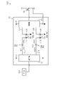
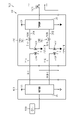
- FIG. 4 is a schematic circuit diagram of the gate driver of the first embodiment
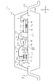
- FIG. FIG. 2 is a plan view showing the internal configuration of the gate driver of the first embodiment
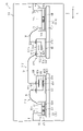
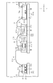
- FIG. 3 is a cross-sectional view schematically showing a part of the cross-sectional structure taken along line 3-3 of FIG. 2
- FIG. 8 is a plan view showing the internal configuration of the gate driver of the second embodiment
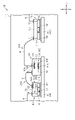
- FIG. 5 is a cross-sectional view schematically showing a part of the cross-sectional structure taken along line 5-5 of FIG. 4
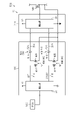
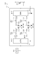
- FIG. 10 is a schematic circuit diagram of a gate driver according to a third embodiment
- FIG. 5 is a schematic cross-sectional view of a gate driver according to a third embodiment; The top view which shows the internal structure of the gate driver of 4th Embodiment.
- FIG. 9 is a cross-sectional view schematically showing a part of the cross-sectional structure taken along line 9-9 of FIG. 8; The typical circuit diagram of the gate driver of 5th Embodiment.
- FIG. 5 is a schematic cross-sectional view of a gate driver according to a fifth embodiment; The typical circuit diagram of the gate driver of 6th Embodiment. Typical sectional drawing of the insulation module of 6th Embodiment. The typical circuit diagram of the gate driver of 7th Embodiment. Typical sectional drawing of the low-voltage circuit unit of 7th Embodiment.
- FIG. 11 is a schematic cross-sectional view of a high-voltage circuit unit according to an eighth embodiment
- FIG. 4 is a schematic cross-sectional view of a gate driver of a modified example
- FIG. 4 is a schematic cross-sectional view of a gate driver of a modified example
- FIG. 4 is a schematic cross-sectional view of a gate driver of a modified example
- FIG. 4 is a schematic circuit diagram of a gate driver of a modification
- FIG. 4 is a schematic circuit diagram of a gate driver of a modification;
- FIG. 1 shows a simplified example of the circuit configuration of the gate driver 10. As shown in FIG.
- the gate driver 10 applies a driving voltage signal to the gates of switching elements, and is applied, for example, to an inverter device 500 mounted on an electric vehicle or a hybrid vehicle.
- the inverter device 500 includes a pair of switching elements 501 and 502 connected in series, a gate driver 10 , and an ECU 503 that controls the gate driver 10 .
- a switching element 501 is a high-side switching element connected to, for example, a drive power supply
- a switching element 502 is a low-side switching element.
- Examples of switching elements 501 and 502 include transistors such as SiMOSFETs, SiCMOSFETs, and IGBTs.
- the gate driver 10 of the first embodiment applies drive voltage signals to the gates of the switching elements 501 . In the following description, it is assumed that the switching elements 501 and 502 are MOSFETs.
- the gate driver 10 is provided for each of the switching elements 501 and 502, and drives the switching elements 501 and 502 individually. In the first embodiment, for convenience of explanation, the gate driver 10 that drives the switching element 501 will be explained.
- the gate driver 10 includes a low voltage circuit 20 to which a first voltage V1 is applied, a high voltage circuit 30 to which a second voltage V2 higher than the first voltage V1 is applied, a transformer 40, and a capacitor 50. .
- the first voltage V1 and the second voltage V2 are DC voltages.
- a signal is transmitted from the low voltage circuit 20 to the high voltage circuit 30 via the transformer 40 and the capacitor 50 based on the control signal from the ECU 503 as an external control device. is configured to output a drive voltage signal from .
- the control signal from the ECU 503 corresponds to an external command.
- a signal transmitted from low-voltage circuit 20 to high-voltage circuit 30, that is, a signal output from low-voltage circuit 20 is, for example, a signal for driving switching element 501, and examples include a set signal and a reset signal.
- the set signal is a signal that transmits the rise of the control signal from the ECU 503, and the reset signal is the signal that transmits the fall of the control signal from the ECU 503. It can also be said that the set signal and the reset signal are signals for generating a drive voltage signal for the switching element 501 . Therefore, the set signal and the reset signal correspond to the first signal.
- the low-voltage circuit 20 is a circuit that operates when the first voltage V1 is applied.
- the low voltage circuit 20 is a circuit electrically connected to the ECU 503 and generates a set signal and a reset signal based on control signals input from the ECU 503 .
- the low-voltage circuit 20 generates a set signal in response to rising of the control signal and generates a reset signal in response to falling of the control signal.
- the low-voltage circuit 20 then transmits the generated set signal and reset signal to the high-voltage circuit 30 .
- the high voltage circuit 30 is a circuit that operates when the second voltage V2 is applied.
- High-voltage circuit 30 is a circuit electrically connected to the gate of switching element 501, and generates a drive voltage signal for driving switching element 501 based on the set signal and reset signal received from low-voltage circuit 20. , the drive voltage signal is applied to the gate of the switching element 501 .
- the high voltage circuit 30 generates a drive voltage signal to be applied to the gate of the switching element 501 based on the first signal output from the low voltage circuit 20 .
- the high-voltage circuit 30 generates a driving voltage signal for turning on the switching element 501 based on the set signal, and applies it to the gate of the switching element 501 .
- the high voltage circuit 30 generates a drive voltage signal for turning off the switching element 501 based on the reset signal, and applies the drive voltage signal to the gate of the switching element 501 .
- the gate driver 10 controls on/off of the switching element 501 .
- the high-voltage circuit 30 has, for example, an RS-type flip-flop circuit to which a set signal and a reset signal are input, and a driver section that generates a drive voltage signal based on the output signal of the RS-type flip-flop circuit.
- the specific circuit configuration of the high voltage circuit 30 is arbitrary.
- Both the transformer 40 and the capacitor 50 are provided between the low voltage circuit 20 and the high voltage circuit 30 . That is, the low voltage circuit 20 and the high voltage circuit 30 are electrically connected via the transformer 40 and the capacitor 50 .
- the capacitor 50 is circuit-wise provided between the transformer 40 and the high-voltage circuit 30, and the transformer 40 and the capacitor 50 are connected in series.
- the low voltage circuit 20 and the high voltage circuit 30 are insulated by the transformer 40 and the capacitor 50 .
- the transformer 40 and the capacitor 50 restrict the transmission of DC voltage between the low-voltage circuit 20 and the high-voltage circuit 30, while allowing the transmission of various signals such as a set signal and a reset signal. ing.
- the state in which the low-voltage circuit 20 and the high-voltage circuit 30 are insulated means a state in which the transmission of the DC voltage between the low-voltage circuit 20 and the high-voltage circuit 30 is interrupted. Transmission of signals to and from the circuit 30 is permitted.
- the dielectric strength of the gate driver 10 is, for example, 2500 Vrms or more and 7500 Vrms or less.
- the withstand voltage of the gate driver 10 of the first embodiment is approximately 3750 Vrms.
- the specific numeric value of the dielectric breakdown voltage of the gate driver 10 is not limited to this and is arbitrary.
- the dielectric breakdown voltage of the transformer 40 in the first embodiment is, for example, 2500 Vrms or more and 7500 Vrms or less. Note that the dielectric breakdown voltage of the transformer 40 may be 2500 Vrms or more and 5700 Vrms or less. However, the dielectric strength of the transformer 40 is not limited to this, and is arbitrary.
- the dielectric strength voltage of the capacitor 50 is set to be equal to or higher than the dielectric strength voltage of the transformer 40, for example.
- the dielectric breakdown voltage of the capacitor 50 is 200 Vrms or more and 5700 Vrms or less, preferably 600 Vrms or more and 5700 Vrms or less.
- the dielectric strength voltage of the capacitor 50 is not limited to be equal to or higher than the dielectric strength voltage of the transformer 40, and the dielectric strength voltage of the capacitor 50 may be lower than the dielectric strength voltage of the transformer 40. .
- the ground of the low voltage circuit 20 and the ground of the high voltage circuit 30 are provided independently.
- the ground potential of the low-voltage circuit 20 will be referred to as a first reference potential
- the ground potential of the high-voltage circuit 30 will be referred to as a second reference potential.
- the first voltage V1 is the voltage from the first reference potential
- the second voltage V2 is the voltage from the second reference potential.
- the first voltage V1 is, for example, 4.5V or more and 5.5V or less
- the second voltage V2 is, for example, 9V or more and 24V or less.
- the gate driver 10 of the first embodiment includes two transformers 40 and two capacitors 50 for transmitting two types of signals from the low voltage circuit 20 to the high voltage circuit 30 .
- the gate driver 10 includes a transformer 40 and a capacitor 50 used for transmitting set signals, and a transformer 40 and capacitors 50 used for transmitting reset signals.
- transformer 40A and capacitor 50A the transformer 40 and capacitor 50 used for transmitting the set signal
- transformer 40B and capacitor 50B the transformer 40 and capacitor 50 used for transmitting the reset signal
- the transformer 40 can be said to include the transformers 40A and 40B
- the capacitor 50 can be said to include the capacitors 50A and 50B.
- the gate driver 10 includes a low-voltage signal line 21A connecting the low-voltage circuit 20 and the transformer 40A, and a low-voltage signal line 21B connecting the low-voltage circuit 20 and the transformer 40B. Therefore, the low-voltage signal line 21A is a signal line through which a set signal is transmitted, and the low-voltage signal line 21B is a signal line through which a reset signal is transmitted.
- the gate driver 10 includes a high voltage signal line 31A that connects the transformer 40A and the high voltage circuit 30, and a high voltage signal line 31B that connects the transformer 40B and the high voltage circuit 30. Therefore, the high-voltage signal line 31A is a signal line through which a set signal is transmitted, and the high-voltage signal line 31B is a signal line through which a reset signal is transmitted.
- the transformer 40A and the capacitor 50A are connected in series by the high voltage signal line 31A, and the capacitor 50A and the high voltage circuit 30 are connected by the high voltage signal line 31A. Therefore, it can be said that the transformer 40A and the high-voltage circuit 30 are electrically connected via the capacitor 50A.
- the transformer 40B and the capacitor 50B are connected in series by the high voltage signal line 31B, and the capacitor 50B and the high voltage circuit 30 are connected by the high voltage signal line 31B. Therefore, it can be said that the transformer 40B and the high-voltage circuit 30 are electrically connected via the capacitor 50B.
- the set signal output from the low voltage circuit 20 is transmitted to the high voltage circuit 30 via the transformer 40A and the capacitor 50A.
- the reset signal output from low voltage circuit 20 is transmitted to high voltage circuit 30 via transformer 40B and capacitor 50B.
- the transformer 40A has a first coil 41A and a second coil 42A that is insulated from the first coil 41A and can be magnetically coupled.
- the first coil 41A is connected to the low-voltage circuit 20 by the low-voltage signal line 21A, and is also connected to the ground of the low-voltage circuit 20. As shown in FIG. That is, the first end of the first coil 41A is electrically connected to the low voltage circuit 20, and the second end of the first coil 41A is electrically connected to the ground of the low voltage circuit 20. Therefore, the potential of the second end of the first coil 41A becomes the first reference potential.
- the first reference potential is 0V, for example.
- the second coil 42A is connected to the high voltage circuit 30 by the high voltage signal line 31A, and is also connected to the ground of the high voltage circuit 30. That is, the first end of the second coil 42A is electrically connected to the high voltage circuit 30, and the second end of the second coil 42A is electrically connected to the ground of the high voltage circuit 30. Therefore, the potential of the second end of the second coil 42A becomes the second reference potential.
- the second reference potential fluctuates as the inverter device 500 is driven, and may become, for example, 600V or higher.
- the capacitor 50A has an insulated first electrode 51A and second electrode 52A.
- the first electrode 51A is electrically connected to the transformer 40A, and the second electrode 52A is electrically connected to the high voltage circuit 30. As shown in FIG. More specifically, the first electrode 51A is connected to the second coil 42A by the high voltage signal line 31A, and the second electrode 52A is connected to the high voltage circuit 30 by the high voltage signal line 31A.
- the transformer 40B has a first coil 41B electrically connected to the low-voltage circuit 20 by a low-voltage signal line 21B, and a second coil 42B insulated from the first coil 41B and capable of magnetic coupling. .
- the second coil 42B is electrically connected to the high voltage circuit 30 via the capacitor 50B.
- the capacitor 50B has an insulated first electrode 51B and second electrode 52B.
- the first electrode 51B is electrically connected to the transformer 40B
- the second electrode 52B is electrically connected to the high voltage circuit 30.
- FIG. Since the transformer 40B and the capacitor 50B are similar to the transformer 40A and the capacitor 50A, detailed description thereof will be omitted.
- FIG. 2 shows an example of a plan view showing the internal configuration of the gate driver 10
- FIG. 3 shows a cross-sectional view taken along line 3-3 of FIG.
- the number of external terminals of the gate driver 10 in FIG. 2 is greater than the number of external terminals of the gate driver 10 in FIG.
- the number of external terminals of the gate driver 10 is the number of external electrodes that can be connected between the gate driver 10 and electronic components outside the gate driver 10 such as the ECU 503 and the switching element 501 (see FIG. 1).
- the number of signal lines (the number of wires W described later) for transmitting signals from the low-voltage circuit 20 to the high-voltage circuit 30 in the gate driver 10 in FIG. 2 is greater than the number of signal lines in the gate driver 10 in FIG.
- the gate driver 10 is a semiconductor device in which a plurality of semiconductor chips are packaged into one package, and is mounted on a circuit board provided in the inverter device 500, for example.
- the switching elements 501 and 502 are mounted on a mounting board different from the circuit board.
- a cooler is attached to the mounting board.
- the package format of the gate driver 10 is the SO system, which is the SOP in the first embodiment.
- the gate driver 10 includes a low-voltage circuit chip 60, a high-voltage circuit chip 70, and a transformer chip 80 as semiconductor chips, a low-voltage lead frame 90 on which the low-voltage circuit chip 60 is mounted, and a high-voltage lead frame on which the high-voltage circuit chip 70 is mounted. 100, and a sealing resin 110 for sealing a part of each lead frame 90, 100 and each chip 60, 70, 80.
- the sealing resin 110 is indicated by a chain double-dashed line for the convenience of explaining the internal structure of the gate driver 10.
- the package format of the gate driver 10 can be arbitrarily changed.
- the sealing resin 110 is made of an electrically insulating material, such as a black epoxy resin.
- the sealing resin 110 is formed in a rectangular plate shape having a thickness direction in the z direction.
- the sealing resin 110 has four resin side surfaces 111-114. Specifically, the sealing resin 110 has resin side surfaces 111 and 112 as both end surfaces in the x direction and resin side surfaces 113 and 114 as both end surfaces in the y direction.
- the x-direction and y-direction are directions orthogonal to the z-direction.
- the x-direction and y-direction are orthogonal to each other.
- planar view means viewing from the z direction.
- the low-voltage lead frame 90 and the high-voltage lead frame 100 are each made of a conductor, and made of Cu (copper) in the first embodiment.
- Each lead frame 90 , 100 is provided across the inside and outside of the sealing resin 110 .
- the low voltage lead frame 90 has a low voltage die pad 91 arranged in the sealing resin 110 and a plurality of low voltage leads 92 arranged across the inside and outside of the sealing resin 110 .
- Each low-voltage lead 92 constitutes an external terminal electrically connected to an external electronic device such as the ECU 503 (see FIG. 1).
- a low voltage circuit chip 60 and a transformer chip 80 are mounted on the low voltage die pad 91 .
- the low-voltage die pad 91 is arranged such that its y-direction center is closer to the resin side surface 113 than the y-direction center of the sealing resin 110 .
- the low voltage die pad 91 is not exposed from the sealing resin 110 .
- the shape of the low-voltage die pad 91 in a plan view is a rectangular shape in which the x direction is the long side direction and the y direction is the short side direction.
- a plurality of low-voltage leads 92 are arranged apart from each other in the x-direction.
- Each of the low-voltage leads 92 arranged at both ends in the x direction among the plurality of low-voltage leads 92 is integrated with the low-voltage die pad 91 .
- a portion of each low-voltage lead 92 protrudes outward from the sealing resin 110 from the resin side surface 113 .
- the high voltage lead frame 100 has a high voltage die pad 101 arranged in the sealing resin 110 and a plurality of high voltage leads 102 arranged across the inside and outside of the sealing resin 110 .
- Each high-voltage lead 102 constitutes an external terminal electrically connected to an external electronic device such as the gate of the switching element 501 (see FIG. 1).
- a high voltage circuit chip 70 is mounted on the high voltage die pad 101 .
- the high voltage die pad 101 is arranged closer to the resin side surface 114 than the low voltage die pad 91 in the y direction.
- high voltage die pad 101 is not exposed from sealing resin 110 .
- the shape of the high-voltage die pad 101 in plan view is a rectangular shape in which the x direction is the long side direction and the y direction is the short side direction.
- the low voltage die pad 91 and the high voltage die pad 101 are spaced apart in the y direction. Therefore, the y-direction can also be said to be the direction in which the die pads 91 and 101 are arranged.
- the y-direction dimensions of the low-voltage die pad 91 and the high-voltage die pad 101 are set according to the size and number of semiconductor chips to be mounted. In the first embodiment, the low-voltage die pad 91 has the low-voltage circuit chip 60 and the transformer chip 80 mounted thereon, and the high-voltage die pad 101 has the high-voltage circuit chip 70 mounted thereon. larger than the dimension in the y direction.
- a plurality of high-voltage leads 102 are arranged apart from each other in the x-direction.
- a pair of high voltage leads 102 among the plurality of high voltage leads 102 are integrated with the high voltage die pad 101 .
- a portion of each high-voltage lead 102 protrudes outward from the sealing resin 110 from the resin side surface 114 .
- the number of high voltage leads 102 is the same as the number of low voltage leads 92 .
- the plurality of low-voltage leads 92 and the plurality of high-voltage leads 102 are arranged in a direction (x-direction) orthogonal to the arrangement direction (y-direction) of the low-voltage die pads 91 and the high-voltage die pads 101 .
- the number of high voltage leads 102 and the number of low voltage leads 92 can be changed arbitrarily.
- the low voltage die pad 91 is supported by a pair of low voltage leads 92 integrated with the low voltage die pad 91, and the high voltage die pad 101 is supported by a pair of high voltage leads 102 integrated with the high voltage die pad 101.
- die pads 91 and 101 are not provided with suspension leads exposed to resin side surfaces 111 and 112 . Therefore, the creepage distance between the low-voltage lead frame 90 and the high-voltage lead frame 100 can be increased.
- the low-voltage circuit chip 60, high-voltage circuit chip 70, and transformer chip 80 are arranged apart from each other in the y direction. In other words, it can be said that the low-voltage circuit chip 60, the high-voltage circuit chip 70, and the transformer chip 80 are arranged apart from each other in the arrangement direction of the die pads 91 and 101 in plan view. In the first embodiment, the low-voltage circuit chip 60, the transformer chip 80, and the high-voltage circuit chip 70 are arranged in this order from the resin side surface 113 to the resin side surface 114 in the y direction.
- the leads 92 and 102 are arranged in the x direction
- the x direction can be said to be the arrangement direction of the leads 92 and 102
- the y direction is the arrangement direction of the leads 92 and 102 in plan view.
- the low voltage circuit chip 60 includes the low voltage circuit 20 shown in FIG.
- the shape of the low-voltage circuit chip 60 in plan view is a rectangle having short sides and long sides.
- the low-voltage circuit chip 60 is mounted on the low-voltage die pad 91 so that the long side extends along the x direction and the short side extends along the y direction.
- the low-voltage circuit chip 60 has a chip main surface 60s and a chip rear surface 60r facing opposite sides in the z-direction.
- a chip rear surface 60r of the low-voltage circuit chip 60 is bonded to a low-voltage die pad 91 with a conductive bonding material SD such as solder or Ag (silver) paste.
- a plurality of first electrode pads 61, a plurality of second electrode pads 62, and a plurality of third electrode pads 63 are formed on the chip main surface 60s of the low-voltage circuit chip 60.
- FIG. Each electrode pad 61-63 is electrically connected to the low-voltage circuit 20 shown in FIG.
- the plurality of first electrode pads 61 are arranged closer to the low-voltage lead 92 than the center of the chip main surface 60s in the y direction in the chip main surface 60s.
- the plurality of first electrode pads 61 are arranged in the x direction.
- the plurality of second electrode pads 62 are arranged at the end portion closer to the transformer chip 80 among both end portions in the y direction of the chip main surface 60s.
- the plurality of second electrode pads 62 are arranged in the x direction.
- the plurality of third electrode pads 63 are arranged at both ends in the x direction of the chip main surface 60s.
- the transformer chip 80 includes the transformer 40 shown in FIG.
- the shape of the transformer chip 80 in plan view is a rectangle having short sides and long sides.
- the transformer chip 80 is mounted on the low-voltage die pad 91 so that its long sides are along the x-direction and its short sides are along the y-direction in plan view.
- the transformer chip 80 is arranged next to the low voltage circuit chip 60 in the y direction.
- the transformer chip 80 is arranged closer to the high voltage circuit chip 70 than the low voltage circuit chip 60 is.
- the transformer chip 80 has a chip main surface 80s and a chip rear surface 80r facing opposite sides in the z-direction.
- a chip rear surface 80r of the transformer chip 80 is bonded to a low-voltage die pad 91 with a conductive bonding material SD.
- a plurality of first electrode pads 81 and a plurality of second electrode pads 82 are formed on the chip main surface 80s of the transformer chip 80 .
- the plurality of first electrode pads 81 are arranged, for example, at the end portion closer to the low-voltage circuit chip 60 among both end portions in the y direction of the chip main surface 80s.
- the plurality of first electrode pads 81 are arranged in the x direction.
- the plurality of second electrode pads 82 are arranged near the center of the chip main surface 80s in the y direction.
- the plurality of second electrode pads 82 are arranged in the x direction.
- the distance between the high-voltage circuit chip 70 and the transformer chip 80 is longer than the distance between the low-voltage circuit chip 60 and the transformer chip 80 .
- the transformer chip 80 includes both transformers 40A and 40B (see FIG. 1), and more specifically, both transformers 40A and 40B are integrated into one chip.
- the transformer chip 80 has an insulating layer 83, and both coils 41A and 42A of the transformer 40A are embedded in the insulating layer 83 and arranged to face each other in the z-direction with the insulating layer 83 interposed therebetween.
- the insulating layer 83 may be a single layer or a plurality of layers.
- Each coil 41A, 42A consists of a conductor layer embedded in the insulating layer 83.
- the second coil 42A is arranged at a position distant from the low voltage die pad 91 with respect to the first coil 41A.
- the first coil 41A is electrically connected to the first electrode pad 81.
- the second coil 42A is electrically connected to the second electrode pad 82. As shown in FIG. Note that the positional relationship between the two coils 41A and 42A can be changed arbitrarily.
- the transformer 40B has the same configuration as the transformer 40A. Therefore, the first coil 41B of the transformer 40B is electrically connected to a first electrode pad 81 different from the first electrode pad 81 electrically connected to the first coil 41A.
- the second coil 42B is electrically connected to a second electrode pad 82 different from the second electrode pad 82 electrically connected to the second coil 42A.
- the high voltage circuit chip 70 includes the high voltage circuit 30 .
- the shape of the high-voltage circuit chip 70 in plan view is a rectangular shape having short sides and long sides.
- the high-voltage circuit chip 70 is mounted on the high-voltage die pad 101 so that the long side extends along the x direction and the short side extends along the y direction.
- the high-voltage circuit chip 70 has a chip main surface 70s and a chip rear surface 70r facing opposite sides in the z-direction.
- a chip rear surface 70r of the high voltage circuit chip 70 is bonded to the high voltage die pad 101 with a conductive bonding material SD.
- capacitors 50A and 50B (see FIG. 1) of the first embodiment are incorporated in a high-voltage circuit chip 70.
- the high-voltage circuit chip 70 has an insulating layer 74 in which both capacitors 50A and 50B are embedded.
- insulating layer 74 is composed of a dielectric.
- the insulating layer 74 is made of SiO2 , for example.
- the high voltage circuit 30 is provided closer to the chip rear surface 70 r of the high voltage circuit chip 70 than the insulating layer 74 .
- the capacitor 50A is arranged in a portion close to the transformer chip 80 in the high voltage circuit chip 70 in the y direction.
- the capacitor 50A is arranged in the high voltage circuit chip 70 closer to the chip main surface 70s than the high voltage circuit 30 is.
- the capacitor 50A is arranged at a position overlapping the high-voltage circuit 30 in plan view. Note that the arrangement position of the capacitor 50A in the high-voltage circuit chip 70 can be arbitrarily changed.
- Each of the first electrode 51A and the second electrode 52A of the capacitor 50A is formed in a flat plate shape facing in the direction orthogonal to the z direction.
- the first electrode 51A and the second electrode 52A are arranged to face each other while being separated from each other in the z direction with the insulating layer 74 interposed therebetween.
- An insulating layer 74 is interposed between the first electrode 51A and the second electrode 52A in the high-voltage circuit chip 70 .
- the first electrode 51A is arranged closer to the chip main surface 70s than the second electrode 52A.
- the arrangement configuration of the capacitor 50B in the high-voltage circuit chip 70 is the same as that of the capacitor 50A.
- the second electrodes 52A and 52B of the capacitors 50A and 50B are electrically connected to the high voltage circuit 30 inside the high voltage circuit chip 70 .
- the capacitors 50A and 50B are electrically connected to the high voltage circuit 30 inside the high voltage circuit chip 70 .
- a plurality of first electrode pads 71, a plurality of second electrode pads 72, and a plurality of third electrode pads 73 are formed on the chip main surface 70s of the high-voltage circuit chip 70.
- FIG. The plurality of first electrode pads 71 are arranged at the end portion closer to the transformer chip 80 among both end portions in the y direction of the chip main surface 70s.
- the plurality of first electrode pads 71 are arranged in the x direction.
- the plurality of second electrode pads 72 are arranged at the end portion farther from the transformer chip 80 among both end portions in the y direction of the chip main surface 70s.
- the multiple second electrode pads 72 are arranged in the x direction.
- the plurality of third electrode pads 73 are arranged at both ends in the x direction of the chip main surface 70s.
- the plurality of first electrode pads 71 are electrically connected to capacitors 50A and 50B (see FIG. 1). Specifically, some of the plurality of first electrode pads 71 are electrically connected to the first electrode 51A (see FIG. 1) of the capacitor 50A. Another part of the multiple first electrode pads 71 is electrically connected to the first electrode 51B (see FIG. 1) of the capacitor 50B. Each of the plurality of second electrode pads 72 and the plurality of third electrode pads 73 is electrically connected to the high voltage circuit 30 (see FIG. 1).
- a plurality of wires W are connected to each of the low-voltage circuit chip 60, the transformer chip 80, and the high-voltage circuit chip .
- Each wire W is a bonding wire formed by a wire bonding apparatus, and is made of a conductor such as Au (gold), Al (aluminum), Cu, or the like.
- the low-voltage circuit chip 60 is electrically connected to the low-voltage lead frame 90 by wires W.
- wires W connect the plurality of first electrode pads 61 of the low-voltage circuit chip 60 to the plurality of low-voltage leads 92 .
- a plurality of third electrode pads 63 of the low-voltage circuit chip 60 and a pair of low-voltage leads 92 integrated with the low-voltage die pad 91 among the plurality of low-voltage leads 92 are connected by wires W.
- FIG. Thereby, the low-voltage circuit 20 (see FIG. 1) and the plurality of low-voltage leads 92 (external electrodes electrically connected to the ECU 503 among the external electrodes of the gate driver 10) are electrically connected.
- the low-voltage die pad 91 since a pair of low-voltage leads 92 integrated with the low-voltage die pad 91 constitute ground terminals, and the low-voltage circuit 20 and the low-voltage die pad 91 are electrically connected by wires W, the low-voltage die pad 91 becomes the same potential as the ground of the low voltage circuit 20 .
- the low-voltage circuit chip 60 and the transformer chip 80 are electrically connected by a wire W.
- wires W connect the plurality of second electrode pads 62 of the low-voltage circuit chip 60 to the plurality of first electrode pads 81 of the transformer chip 80 .
- the low-voltage circuit 20 and the first coils 41A and 41B (see FIG. 1) of the transformers 40A and 40B are electrically connected.
- the first coils 41A and 41B are composed of a first electrode pad 81, a wire W connecting the low-voltage circuit chip 60 and the transformer chip 80, a second electrode pad 62, the low-voltage circuit 20, and a third electrode pad 63. , and a wire W connected to the third electrode pad 63 , to the low-voltage die pad 91 . Thereby, the first coils 41A and 41B of the transformers 40A and 40B and the ground of the low voltage circuit 20 are electrically connected.
- a wire W electrically connects the transformer chip 80 and the high-voltage circuit chip 70 .
- wires W connect the plurality of second electrode pads 82 of the transformer chip 80 to the plurality of first electrode pads 71 of the high-voltage circuit chip 70 .
- the second coil 42A of the transformer 40A and the first electrode 51A of the capacitor 50A are electrically connected
- the second coil 42B of the transformer 40B and the first electrode 51B of the capacitor 50B are electrically connected.
- the second electrode 52A of the capacitor 50A is electrically connected to the high voltage circuit 30 inside the high voltage circuit chip 70.
- the portion of the high voltage signal line 31A that connects the second electrode 52A and the high voltage circuit 30 is incorporated in the high voltage circuit chip 70 .
- the high voltage circuit chip 70 and the plurality of high voltage leads 102 of the high voltage lead frame 100 are electrically connected by wires W, respectively.
- wires W connect the plurality of second electrode pads 72 and the plurality of third electrode pads 73 of the high voltage circuit chip 70 to the plurality of high voltage leads 102 .
- the high voltage circuit 30 and the plurality of high voltage leads 102 (the external electrodes of the gate driver 10 that are electrically connected to the inverter device 500 such as the switching element 501) are electrically connected.
- the pair of high-voltage leads 102 integrated with the high-voltage die pad 101 form a ground terminal, and the wires W electrically connect the high-voltage circuit 30 and the high-voltage die pad 101. Therefore, the high-voltage die pad 101 becomes the same potential as the ground of the high voltage circuit 30 .
- each coil 42A, 42B includes a second electrode pad 82, a wire W connecting the transformer chip 80 and the high-voltage circuit chip 70, a first electrode pad 71, a high-voltage circuit 30, and a third electrode pad.
- 73 and the wire W connected to the high voltage lead 102 integrated with the high voltage die pad 101 among the wires W connected to the third electrode pad 73 is electrically connected to the high voltage die pad 101 .
- the ground potential of the high voltage circuit 30 may become higher than the ground potential of the low voltage circuit 20 .
- a current may flow from the ground of the high voltage circuit 30 to the ground of the low voltage circuit 20 .
- a transformer 40 having an insulating structure is provided between the low-voltage circuit 20 and the high-voltage circuit 30 .
- Capacitor 50 maintains isolation between low voltage circuit 20 and high voltage circuit 30 .
- the capacitor 50 functions as additional insulation with respect to the transformer 40 that serves as basic insulation.
- the gate driver 10 of the first embodiment the following effects are obtained.
- (1-1) In the gate driver 10, the low-voltage circuit 20 to which the first voltage V1 is applied and the high-voltage circuit 30 to which the second voltage V2 higher than the first voltage V1 is applied are mutually connected via the insulating layer 83.
- a transformer 40 having first coils 41A, 41B and second coils 42A, 42B arranged opposite to each other, and a capacitor 50 connected in series to the transformer 40 are provided.
- Low-voltage circuit 20 and high-voltage circuit 30 transmit signals via transformer 40 and capacitor 50 .
- both the transformer 40 and the capacitor 50 connected in series with the transformer 40 insulate the low-voltage circuit 20 and the high-voltage circuit 30, in the transformer 40, the first coil 41A (41B) and the Even if dielectric breakdown occurs due to a short circuit with the second coil 42A (42B), the insulation between the low-voltage circuit 20 and the high-voltage circuit 30 can be maintained by the capacitor 50. FIG. Therefore, it is possible to improve safety.
- the capacitor 50A has a first electrode 51A and a second electrode 52A.
- the first electrode 51A is electrically connected to the transformer 40A, and the second electrode 52A is electrically connected to the high voltage circuit 30.
- the capacitor 50B has a first electrode 51B and a second electrode 52B.
- the first electrode 51B is electrically connected to the transformer 40B, and the second electrode 52B is electrically connected to the high voltage circuit 30.
- the capacitor 50A can insulate the high-voltage circuit 30 from the transformer 40A.
- the capacitor 50B can insulate the high voltage circuit 30 side of the transformer 40B. Therefore, application of a high voltage such as the drain voltage of the switching element 501 to the low-voltage lead frame 90 due to the dielectric breakdown of the transformers 40A and 40B can be suppressed.
- the gate driver 10 includes a low voltage circuit chip 60 including the low voltage circuit 20, a high voltage circuit chip 70 including the high voltage circuit 30, and a transformer chip 80 including the transformers 40A and 40B.
- the transformer chip 80 is provided separately from the low-voltage circuit chip 60 and the high-voltage circuit chip 70, the common transformer chip 80 can be used for different low-voltage circuit chips 60 and high-voltage circuit chips 70. can.
- manufacturing costs can be reduced when manufacturing multiple types of gate drivers in which at least one of the low-voltage circuit chip 60 and the high-voltage circuit chip 70 is different.
- the capacitors 50A and 50B are incorporated in the high voltage circuit chip 70. With this configuration, the number of semiconductor chips in the gate driver 10 can be reduced compared to the case where the capacitors 50A and 50B are configured as independent chips. Therefore, an increase in size of the gate driver 10 can be suppressed.
- the high-voltage circuit chip 70 is mounted on the high-voltage die pad 101, even if dielectric breakdown occurs due to a short circuit between the first coil 41A (41B) and the second coil 42A (42B) in the transformer 40, However, it is difficult for the high voltage to reach the low voltage lead frame 90 . Thereby, application of a high voltage to the low-voltage lead frame 90 can be suppressed.
- the capacitors 50A and 50B are arranged at positions overlapping the high-voltage circuit 30 in plan view. With this configuration, it is possible to suppress the increase in size of the high-voltage circuit chip 70 .
- the capacitors 50A and 50B are arranged near the transformer chip 80 in the high-voltage circuit chip 70 . With this configuration, both the conductive path between the transformer 40A and the capacitor 50A and the conductive path between the transformer 40B and the capacitor 50B can be shortened. Therefore, the inductance caused by the length of these conductive paths can be reduced.
- the transformer chip 80 is arranged between the low voltage circuit chip 60 and the high voltage circuit chip 70 . According to this configuration, when the chips 60, 70, 80 are electrically connected by connecting the chips 60, 70, 80 adjacent to each other in the arrangement direction (y direction) of the chips 60, 70, 80 with the wires W, the wires Since it is not necessary for W to straddle predetermined chips, the connection structure of the wire W can be simplified.
- the dielectric strength voltage of the capacitor 50 is set to be equal to or higher than the dielectric strength voltage of the transformer 40 . According to this configuration, even if dielectric breakdown occurs due to a short circuit between the first coil 41A (41B) and the second coil 42A (42B) in the transformer 40, driving of the inverter device 500 is stopped. Insulation between the low voltage circuit 20 and the high voltage circuit 30 can be maintained.
- FIG. 4 shows the sealing resin 110 by a chain double-dashed line for the convenience of explaining the internal structure of the gate driver 10 .
- the gate driver 10 includes a low voltage circuit chip 60, a high voltage circuit chip 70, a transformer chip 80, and a capacitor chip 120. These chips 60 , 70 , 80 and 120 are sealed with sealing resin 110 .
- the low-voltage circuit chip 60, high-voltage circuit chip 70, transformer chip 80, and capacitor chip 120 are arranged apart from each other in the y direction. It can be said that these chips 60 , 70 , 80 , 120 are arranged in the arrangement direction of the low-voltage die pad 91 and the high-voltage die pad 101 .
- the low-voltage circuit chip 60 , the transformer chip 80 , the capacitor chip 120 and the high-voltage circuit chip 70 are arranged in this order from the low-voltage lead 92 toward the high-voltage lead 102 .
- the transformer chip 80 and the capacitor chip 120 are arranged between the low-voltage circuit chip 60 and the high-voltage circuit chip 70 in plan view.
- the transformer chip 80 is arranged between the low-voltage circuit chip 60 and the capacitor chip 120
- the capacitor chip 120 is arranged between the transformer chip 80 and the high-voltage circuit chip 70 .
- Both the low voltage circuit chip 60 and the transformer chip 80 are mounted on the low voltage die pad 91 of the low voltage lead frame 90 as in the first embodiment.
- both the capacitor chip 120 and the high voltage circuit chip 70 are mounted on the high voltage die pad 101 of the high voltage leadframe 100 .
- the y-direction length of the high-voltage die pad 101 of the second embodiment is longer than the y-direction length of the high-voltage die pad 101 of the first embodiment.
- the length of high voltage die pad 101 in the y direction is equal to the length of low voltage die pad 91 in the y direction.
- the shape of the capacitor chip 120 in plan view is a rectangle having long sides and short sides.
- the capacitor chip 120 is mounted on the high-voltage die pad 101 so that the long side extends along the x direction and the short side extends along the y direction.
- the capacitor chip 120 has a chip main surface 120s and a chip rear surface 120r facing opposite sides in the z-direction.
- the capacitor chip 120 is bonded to the high voltage die pad 101 with a conductive bonding material SD.
- a plurality of first electrode pads 121 and a plurality of second electrode pads 122 are formed on the chip main surface 120s of the capacitor chip 120 .
- the plurality of first electrode pads 121 are arranged near the transformer chip 80 on the chip main surface 120s.
- the plurality of first electrode pads 121 are arranged in the x direction.
- the plurality of second electrode pads 122 are arranged near the high-voltage circuit chip 70 on the chip main surface 120s.
- the plurality of second electrode pads 122 are arranged in the x direction.
- capacitor chip 120 includes both capacitors 50A and 50B (see FIG. 1), and more specifically, both capacitors 50A and 50B are packaged into one package.
- the capacitor chip 120 has an insulating layer 123, and both electrodes 51A and 52A of the capacitor 50A are embedded in the insulating layer 123 and arranged to face each other in the z direction with the insulating layer 123 interposed therebetween.
- the first electrode 51A is arranged at a position farther from the high-voltage die pad 101 than the second electrode 52A.
- the insulating layer 123 is composed of a dielectric.
- the insulating layer 123 is made of SiO2 , for example. Note that the insulating layer 123 may be a single layer or a plurality of layers.
- the arrangement configuration of the capacitor 50B in the capacitor chip 120 is the same as that of the capacitor 50A.
- Both the capacitors 50A and 50B are electrically connected to the first electrode pad 121 and the second electrode pad 122 inside the capacitor chip 120 .
- the first electrode pad 121 is electrically connected to the first electrode 51A of the capacitor 50A.
- the second electrode pad 122 is electrically connected to the second electrode 52A of the capacitor 50A.
- first electrode pad 121 is electrically connected to the first electrode 51B of the capacitor 50B.
- second electrode pad 122 is electrically connected to the second electrode 52B of the capacitor 50B.
- the arrangement relationship between the electrodes 51B and 52B is the same as that of the electrodes 51A and 52A.
- the capacitor chip 120 is electrically connected by wires W to both the transformer chip 80 and the high-voltage circuit chip 70 .
- the second electrode pad 82 of the transformer chip 80 and the first electrode pad 121 of the capacitor chip 120 are connected by a wire W
- the second electrode pad 122 of the capacitor chip 120 and the first electrode pad 121 of the high voltage circuit chip 70 are connected.
- the electrode pads 71 are connected by wires W.
- the gate driver 10 includes a low voltage circuit chip 60 including the low voltage circuit 20, a high voltage circuit chip 70 including the high voltage circuit 30, a transformer chip 80 including the transformer 40, a capacitor chip 120 including the capacitor 50, It has The low-voltage circuit chip 60, the transformer chip 80, the capacitor chip 120, and the high-voltage circuit chip 70 are arranged in this order.
- the chips 60, 70, 80, 120 are electrically connected by connecting the chips 60, 70, 80, 120 adjacent to each other in the arrangement direction (y direction) with the wire W.
- the connection structure of the wires W can be simplified because the wires W do not need to straddle predetermined chips.
- the transformer chip 80 and the capacitor chip 120 are provided separately from the low-voltage circuit chip 60 and the high-voltage circuit chip 70, respectively, the transformer chip 80 and the common transformer chip 80 are common to different low-voltage circuit chips 60 and high-voltage circuit chips 70. of capacitor chip 120 can be used. As a result, manufacturing costs can be reduced when manufacturing multiple types of gate drivers in which at least one of the low-voltage circuit chip 60 and the high-voltage circuit chip 70 is different.
- the gate driver 10 includes a low voltage die pad 91 on which the low voltage circuit chip 60 is mounted and a high voltage die pad 101 on which the high voltage circuit chip 70 is mounted.
- the transformer chip 80 is mounted on the low voltage die pad 91 and the capacitor chip 120 is mounted on the high voltage die pad 101 .
- the transformer chip 80 and the capacitor chip 120 are mounted separately on the low-voltage die pad 91 and the high-voltage die pad 101, respectively. 101 can be suppressed from becoming excessively large. Therefore, it is possible to suppress the generation of voids in the sealing resin 110 due to excessive increase in the area of one of the die pads 91 and 101 .
- FIG. 6 The gate driver 10 of the third embodiment will be described with reference to FIGS. 6 and 7.
- FIG. The gate driver 10 of the third embodiment differs from the gate driver 10 of the first embodiment mainly in the position where the capacitor 50 is provided.
- differences from the first embodiment will be mainly described, and the same reference numerals will be given to the components common to the gate driver 10 of the first embodiment, and the description thereof will be omitted.
- the capacitor 50 is provided between the low-voltage circuit 20 and the transformer 40 in terms of circuit, unlike the first embodiment. Specifically, the capacitor 50A is circuit-wise provided between the low-voltage circuit 20 and the transformer 40A, and the capacitor 50B is circuit-wise provided between the low-voltage circuit 20 and the transformer 40B. In the third embodiment, the transformer 40A and the capacitor 50A are connected in series. The transformer 40B and the capacitor 50B are connected in series.
- the transformer 40A and the capacitor 50A are connected in series by the low voltage signal line 21A, and the capacitor 50A and the low voltage circuit 20 are connected by the low voltage signal line 21A. Therefore, it can be said that the low-voltage circuit 20 and the transformer 40A are electrically connected via the capacitor 50A.
- the transformer 40B and the capacitor 50B are connected in series by the low voltage signal line 21B, and the capacitor 50B and the low voltage circuit 20 are connected by the low voltage signal line 21B. Therefore, it can be said that the low-voltage circuit 20 and the transformer 40B are electrically connected via the capacitor 50B.
- the capacitor 50A is not provided between the transformer 40A and the high voltage circuit 30 in terms of the circuit, and the capacitor 50B is provided between the transformer 40B and the high voltage circuit 30 in terms of the circuit.
- the gate driver 10 includes a low-voltage circuit chip 60, a high-voltage circuit chip 70, and a transformer chip 80.
- the arrangement configuration of these chips 60, 70, 80 and the configuration of each lead frame 90, 100 are the same as in the first embodiment.
- transformer chip 80 is mounted on low voltage die pad 91 of low voltage lead frame 90 .
- the capacitors 50A and 50B (see FIG. 6) of the third embodiment are incorporated in the low voltage circuit chip 60.
- the low-voltage circuit chip 60 has an insulating layer 64 in which both capacitors 50A and 50B are embedded.
- the first electrode 51A and the second electrode 52A are spaced apart from each other in the z-direction with the insulating layer 64 interposed therebetween.
- capacitors 50A and 50B are arranged in a portion near transformer chip 80 in low-voltage circuit chip 60 in the y direction.
- the insulating layer 64 is composed of a dielectric.
- the insulating layer 64 is made of SiO2 , for example.
- the capacitor 50 is arranged in the low voltage circuit chip 60 closer to the chip main surface 60s than the low voltage circuit 20 is.
- both electrodes 51A and 52A of the capacitor 50A are arranged in the low voltage circuit chip 60 closer to the chip main surface 60s than the low voltage circuit 20 is.
- the capacitors 50A and 50B are arranged at positions overlapping the low voltage circuit 20 in the low voltage circuit chip 60 in plan view. The arrangement positions of the capacitors 50A and 50B in the low-voltage circuit chip 60 can be changed arbitrarily.
- the capacitor 50 is electrically connected to both the low voltage circuit 20 and the second electrode pad 62 of the low voltage circuit chip 60 in the low voltage circuit chip 60 .
- the first electrode 51A of the capacitor 50A is electrically connected to the low voltage circuit 20 within the low voltage circuit chip 60.
- a second electrode 52A of the capacitor 50A is electrically connected to a second electrode pad 62 inside the low voltage circuit chip 60 .
- the capacitor 50B has the same configuration as the capacitor 50A. Both electrodes 51B and 52B of the capacitor 50B are also arranged in the low-voltage circuit chip 60 closer to the chip main surface 60s than the low-voltage circuit 20, and in the low-voltage circuit chip 60, the second electrode pads of the low-voltage circuit 20 and the low-voltage circuit chip 60 are arranged. 62 are electrically connected.
- the second electrode pads 62 are connected to the first electrode pads 81 of the transformer chip 80 by wires W, as in the first embodiment. Specifically, a wire W connects a second electrode pad 62 electrically connected to the second electrode 52A of the capacitor 50A and a first electrode pad 81 electrically connected to the first coil 41A of the transformer 40A. It is although not shown, a wire W connects a second electrode pad 62 electrically connected to the second electrode 52B of the capacitor 50B and a first electrode pad 81 electrically connected to the first coil 41B of the transformer 40B. connected by
- the following effects are obtained. can get.
- (3-1) The first electrode 51A of the capacitor 50A is electrically connected to the low voltage circuit 20, and the second electrode 52A of the capacitor 50A is electrically connected to the transformer 40A.
- a first electrode 51B of the capacitor 50B is electrically connected to the low voltage circuit 20, and a second electrode 52B of the capacitor 50B is electrically connected to the transformer 40B.
- Insulation between the low-voltage circuit 20 and the high-voltage circuit 30 can be maintained by the capacitor 50B even when dielectric breakdown occurs due to a short circuit between the first coil 41B and the second coil 42B in the transformer 40B. can be done. Therefore, application of a high voltage to the low-voltage circuit 20 due to the dielectric breakdown of the transformers 40A and 40B is suppressed, so that application of a high voltage to the low-voltage lead frame 90 can be suppressed.
- the capacitors 50A and 50B are incorporated in the low-voltage circuit chip 60; With this configuration, the number of semiconductor chips in the gate driver 10 can be reduced compared to the case where the capacitors 50A and 50B are configured as independent chips. Therefore, an increase in size of the gate driver 10 can be suppressed.
- the capacitors 50A and 50B are arranged at positions overlapping the low-voltage circuit 20 in plan view. According to this configuration, it is possible to suppress an increase in the size of the low-voltage circuit chip 60 .
- the capacitors 50A and 50B are arranged near the transformer chip 80 in the low-voltage circuit chip 60 .
- both the conductive path between the capacitor 50A and the transformer 40A and the conductive path between the capacitor 50B and the transformer 40B can be shortened. Therefore, the inductance caused by the length of these conductive paths can be reduced.
- FIG. 8 shows the sealing resin 110 with a chain double-dashed line for the convenience of explaining the internal structure of the gate driver 10 .
- the gate driver 10 includes a low voltage circuit chip 60, a high voltage circuit chip 70, a transformer chip 80, and a capacitor chip 120. These chips 60 , 70 , 80 and 120 are sealed with sealing resin 110 .
- the low-voltage circuit chip 60, high-voltage circuit chip 70, transformer chip 80, and capacitor chip 120 are arranged apart from each other in the y direction. It can be said that these chips 60 , 70 , 80 , 120 are arranged in the arrangement direction of the low-voltage die pad 91 and the high-voltage die pad 101 .
- the low-voltage circuit chip 60, the capacitor chip 120, the transformer chip 80, and the high-voltage circuit chip 70 are arranged in this order from the low-voltage lead 92 toward the high-voltage lead .
- capacitor chip 120 and transformer chip 80 are arranged between low-voltage circuit chip 60 and high-voltage circuit chip 70
- capacitor chip 120 is arranged between low-voltage circuit chip 60 and transformer chip 80 .
- the low voltage circuit chip 60 , capacitor chip 120 and transformer chip 80 are mounted on the low voltage die pad 91 of the low voltage lead frame 90 .
- the capacitor chip 120 is bonded to the low-voltage die pad 91 with a conductive bonding material SD (see FIG. 9).
- the shape and arrangement attitude of the capacitor chip 120 in plan view are the same as in the second embodiment.
- the y-direction length of the low-voltage die pad 91 of the fourth embodiment is longer than the y-direction length of the low-voltage die pad 91 of the third embodiment.
- the insulation between the transformer chip 80 and the low voltage die pad 91 can be maintained by sufficiently separating the first coil 41A from the low voltage die pad 91.
- the high voltage die pad 101 of the fourth embodiment is the same as the high voltage die pad 101 of the first embodiment.
- the capacitor chip 120 is electrically connected by wires W to both the low voltage circuit chip 60 and the transformer chip 80 .
- a wire W connects a first electrode pad 121 of the capacitor chip 120 and a second electrode pad 62 of the low-voltage circuit chip 60 .
- a wire W connects the second electrode pad 122 of the capacitor chip 120 and the first electrode pad 81 of the transformer chip 80 .
- a wire W connects a first electrode pad 121 to which the first electrode 51A of the capacitor 50A is electrically connected and a second electrode pad 62 to which the low-voltage circuit 20 is electrically connected. Therefore, the first electrode 51A of the capacitor 50A and the low voltage circuit 20 are electrically connected.
- the wire W connects the second electrode pad 122 electrically connected to the second electrode 52A of the capacitor 50A and the second electrode pad 62 electrically connected to the first coil 41A of the transformer 40A. , the second electrode 52A of the capacitor 50A and the first coil 41A of the transformer 40A are electrically connected.
- the first electrode 51B of the capacitor 50B and the low-voltage circuit 20 are electrically connected in the same manner as the capacitor 50A, and the second electrode 52B of the capacitor 50B and the first coil 41B of the transformer 40B are connected. electrically connected.
- the gate driver 10 of the fourth embodiment in addition to the effect (3-1) of the third embodiment, the following effects can be obtained.
- the gate driver 10 includes a low voltage circuit chip 60 including the low voltage circuit 20, a high voltage circuit chip 70 including the high voltage circuit 30, a transformer chip 80 including the transformer 40, a capacitor chip 120 including the capacitor 50, It has The low-voltage circuit chip 60, the capacitor chip 120, the transformer chip 80, and the high-voltage circuit chip 70 are arranged in this order. According to this configuration, the same effect as (2-1) of the second embodiment can be obtained.
- FIG. 10 of the fifth embodiment differs from the gate driver 10 of the first embodiment in that it has a double insulation structure with a plurality of transformers.
- points different from the first embodiment will be described, and the same reference numerals will be given to the components common to the gate driver 10 of the first embodiment, and description thereof will be omitted.
- the transformer 40A of the transformer 40 has a first transformer 43A and a second transformer 44A connected in series.
- the transformer 40B has a first transformer 43B and a second transformer 44B connected in series. Since each of the transformers 40A and 40B has a double insulation structure in this manner, the dielectric strength voltage of the gate driver 10 is higher than that of the first to fourth embodiments, and is, for example, about 5000 Vrms.
- the first transformer 43A is electrically connected to the low voltage circuit 20.
- the first transformer 43A has a first coil 45A and a second coil 46A that is insulated from the first coil 45A and can be magnetically coupled.
- the second transformer 44A is electrically connected to the high voltage circuit 30. It can also be said that the second transformer 44A is provided on a signal line connecting the first transformer 43A and the high-voltage circuit 30 .
- the second transformer 44A has a first coil 47A and a second coil 48A that is insulated from the first coil 47A and can be magnetically coupled.
- the first coil 45A is electrically connected to the low-voltage circuit 20 by the low-voltage signal line 21A, and is also connected to the ground of the low-voltage circuit 20. That is, the first end of the first coil 45A is electrically connected to the low voltage circuit 20, and the second end of the first coil 45A is electrically connected to the ground of the low voltage circuit 20. Therefore, the potential of the second end of the first coil 45A becomes the first reference potential.
- the first reference potential is 0V, for example.
- the second coil 46A is connected to the first coil 47A of the second transformer 44A.
- the second coil 46A and the first coil 47A are connected together so as to be electrically floating. That is, the first end of the second coil 46A is connected to the first end of the first coil 47A, and the second end of the second coil 46A is connected to the second end of the first coil 47A.
- the second coil 46A and the first coil 47A serve as relay coils that relay transmission of the set signal from the first coil 45A to the second coil 48A.
- the second coil 48A is electrically connected to the high voltage circuit 30 via the capacitor 50A by the high voltage signal line 31A, and is also connected to the ground of the high voltage circuit 30. That is, the first end of the second coil 48A is electrically connected to the high voltage circuit 30 via the capacitor 50A, and the second end of the second coil 48A is electrically connected to the ground of the high voltage circuit 30. . Therefore, the potential at the second end of the second coil 48A becomes the second reference potential.
- the second reference potential fluctuates as inverter device 500 is driven, and becomes, for example, 600 V or higher.
- the capacitor 50A is provided on the high voltage signal line 31A.
- a capacitor 50A is provided between the second transformer 44A and the high voltage circuit 30 . That is, the capacitor 50A is provided on the high voltage signal line 31A that connects the second transformer 44A and the high voltage circuit 30 together.
- the capacitor 50A is connected in series with the second transformer 44A.
- a first electrode 51A of the capacitor 50A is electrically connected to the second coil 48A, and a second electrode 52A of the capacitor 50A is electrically connected to the high voltage circuit 30.
- a first transformer 43B of the transformer 40B has a first coil 45B electrically connected to the low-voltage circuit 20 and a second coil 46B insulated from the first coil 45B and capable of magnetic coupling. .
- a second transformer 44B of the transformer 40B has a first coil 47B electrically connected to the high voltage circuit 30 and a second coil 48B insulated from the first coil 47B and capable of magnetic coupling. . Since the transformer 40B and the capacitor 50B are the same as the transformer 40A and the capacitor 50A, detailed description thereof will be omitted.
- the gate driver 10 includes a low voltage circuit chip 60, a high voltage circuit chip 70, a first transformer chip 80A and a second transformer chip 80B.
- the low-voltage circuit chip 60, the high-voltage circuit chip 70, the first transformer chip 80A, and the second transformer chip 80B are arranged apart from each other in the y direction. It can be said that these chips 60 , 70 , 80 A, 80 B are arranged in the arrangement direction of the low-voltage die pad 91 and the high-voltage die pad 101 .
- the low-voltage circuit chip 60, the first transformer chip 80A, the second transformer chip 80B, and the high-voltage circuit chip 70 are arranged in this order from the low-voltage lead 92 toward the high-voltage lead 102 (see FIG. 2). .
- each transformer chip 80A, 80B is arranged between the low-voltage circuit chip 60 and the high-voltage circuit chip 70 in plan view.
- both the low voltage circuit chip 60 and the first transformer chip 80A are mounted on the low voltage die pad 91 of the low voltage lead frame 90.
- Both the high voltage circuit chip 70 and the second transformer chip 80B are mounted on the high voltage die pad 101 of the high voltage lead frame 100 .
- the first transformer chip 80A includes a first transformer 43A of the transformer 40A and a first transformer 43B of the transformer 40B (see FIG. 10), and more specifically, both transformers 43A and 43B are packaged into one. .
- the first transformer chip 80A includes a transformer arranged closer to the low-voltage circuit 20 than the high-voltage circuit 30 in terms of circuitry among the transformers 40A and 40B.
- the first transformer chip 80A has an insulating layer 83 like the transformer chip 80 of the first embodiment. Both coils 45A and 46A of the first transformer 43A are embedded in an insulating layer 83, and arranged to face each other with the insulating layer 83 interposed therebetween in the z-direction.
- the insulating layer 83 may be one layer, or may be multiple layers.
- Both coils 45A and 46A are composed of conductor layers embedded in the insulating layer 83.
- the second coil 46A is arranged at a position distant from the low voltage die pad 91 with respect to the first coil 45A.
- the first coil 45A is electrically connected to the first electrode pad 81A
- the second coil 46A is electrically connected to the second electrode pad 82A.
- the arrangement configuration of the first transformer 43B in the first transformer chip 80A is the same as that of the first transformer 43A.
- the second transformer chip 80B includes a second transformer 44A of the transformer 40A and a second transformer 44B of the transformer 40B (see FIG. 10), and more specifically, both transformers 44A and 44B are packaged into one. .
- the second transformer chip 80B includes a transformer arranged closer to the high voltage circuit 30 than the low voltage circuit 20 in terms of circuitry among the transformers 40A and 40B.
- the second transformer chip 80B has an insulating layer 83 like the transformer chip 80 of the first embodiment. Both the coils 47A and 48A of the second transformer 44A are embedded in the insulating layer 83 and arranged to face each other with the insulating layer 83 interposed therebetween in the z-direction.
- the insulating layer 83 may be one layer, or may be multiple layers.
- Both coils 47A and 48A are composed of conductor layers embedded in the insulating layer 83.
- the first coil 47A is arranged at a position distant from the high voltage die pad 101 with respect to the second coil 48A.
- the first coil 47A is electrically connected to the first electrode pad 81B
- the second coil 48A is electrically connected to the second electrode pad 82B.
- the arrangement configuration of the second transformer 44B in the second transformer chip 80B is the same as that of the second transformer 44A.
- a wire W connects the low-voltage circuit chip 60 and the first transformer chip 80A. Specifically, a wire W connects the second electrode pad 62 of the low-voltage circuit chip 60 and the first electrode pad 81A of the first transformer chip 80A. Thereby, the low-voltage circuit 20 and the first coil 45A of the first transformer 43A are electrically connected, and the low-voltage circuit 20 and the first coil 45B of the first transformer 43B are electrically connected.
- a wire W connects the first transformer chip 80A and the second transformer chip 80B. Specifically, a wire W connects a second electrode pad 82A of the first transformer chip 80A and a first electrode pad 81B of the second transformer chip 80B. Thereby, the second coil 46A of the first transformer 43A and the first coil 47A of the second transformer 44A are electrically connected, and the second coil 46B of the first transformer 43B and the first coil 47B of the second transformer 44B ( 10) are electrically connected.
- a wire W connects the second transformer chip 80B and the high-voltage circuit chip 70 .
- a wire W connects the second electrode pad 82B of the second transformer chip 80B and the first electrode pad 71 of the high-voltage circuit chip 70 .
- the second coil 48A of the second transformer 44A and the first electrode 51A of the capacitor 50A are electrically connected, and the second coil 48B of the second transformer 44B and the first electrode 51B of the capacitor 50B are connected (see FIG. 10). are electrically connected.
- the transformer 40A has a first transformer 43A and a second transformer 44A connected in series.
- the transformer 40B has a first transformer 43B and a second transformer 44B connected in series.
- the signal line for transmitting the set signal has a double insulation structure between the low-voltage circuit 20 and the high-voltage circuit 30 by the first transformer 43A and the second transformer 44A
- the signal line for transmitting the reset signal has a double insulation structure. Since the first transformer 43B and the second transformer 44B provide a double insulation structure between the low-voltage circuit 20 and the high-voltage circuit 30, the withstand voltage of the gate driver 10 can be improved.
- FIG. 12 and 13 The gate driver 10 of the sixth embodiment will be described with reference to FIGS. 12 and 13.
- FIG. The gate driver 10 of the sixth embodiment mainly differs from the gate driver 10 of the second embodiment in that the gate driver 10 is composed of a plurality of packages.
- points different from the second embodiment will be described, and the same reference numerals will be given to the components common to the gate driver 10 of the second embodiment, and description thereof will be omitted.
- the circuit configuration of the gate driver 10 of the sixth embodiment is the same as that of the gate driver 10 of the first embodiment.
- the gate driver 10 comprises a low voltage circuit module 200 , a high voltage circuit module 210 and an insulation module 220 .
- the low voltage circuit module 200 includes the low voltage circuit 20.
- the low voltage circuit module 200 includes a low voltage circuit chip including the low voltage circuit 20, a low voltage lead frame including a low voltage die pad on which the low voltage circuit chip is mounted, a part of the low voltage lead frame and the low voltage lead frame. and a sealing resin for sealing the circuit chip.
- the high voltage circuit module 210 includes the high voltage circuit 30 .
- the high voltage circuit module 210 includes a high voltage circuit chip including the high voltage circuit 30, a high voltage lead frame including a high voltage die pad on which the high voltage circuit chip is mounted, a part of the high voltage lead frame and a high voltage chip. and a sealing resin for sealing the circuit chip.
- the isolation module 220 enables transmission of set and reset signals from the low voltage circuit 20 to the high voltage circuit 30, while insulating the low voltage circuit 20 and the high voltage circuit 30 from each other. That is, the insulation module 220 is used to insulate the low voltage circuit 20 and the high voltage circuit 30 included in the gate driver 10 .
- Isolation module 220 includes transformer 40 and capacitor 50 . Transformer 40 and capacitor 50 are used to transmit signals (set signal and reset signal) between low-voltage circuit 20 and high-voltage circuit 30, as in the first embodiment. As shown in FIG. 12, the insulation module 220 is arranged between the low voltage circuit 20 and the high voltage circuit 30 in terms of circuit. Therefore, the low voltage circuit 20 and the high voltage circuit 30 are connected via the transformer 40 and the capacitor 50 .
- the insulation module 220 includes a transformer chip 80, a capacitor chip 120, a low voltage lead frame 221, a high voltage lead frame 222, a transformer chip 80, a capacitor chip 120, and lead frames 221 and 222. and a sealing resin 223 that seals a part.
- Each lead frame 221, 222 is made of a conductor, and is made of Cu in the sixth embodiment.
- Each lead frame 221 , 222 is provided across the inside and outside of the sealing resin 223 .
- the low-voltage lead frame 221 is a lead frame electrically connected to the low-voltage circuit 20 (see FIG. 12). and a plurality of low voltage leads 221b disposed thereon.
- Each low-voltage lead 221 b constitutes an external terminal electrically connected to the low-voltage circuit 20 .
- the high-voltage lead frame 222 is a lead frame that is electrically connected to the high-voltage circuit 30 (see FIG. 12). and a plurality of high voltage leads 222b disposed thereon. Each high voltage lead 222 b constitutes an external terminal electrically connected to the high voltage circuit 30 .
- the transformer chip 80 is mounted on the low voltage die pad 221a and the capacitor chip 120 is mounted on the high voltage die pad 222a.
- the low voltage die pad 221a corresponds to the first die pad and the high voltage die pad 222a corresponds to the second die pad.
- the low-voltage lead 221b corresponds to the first lead, and the high-voltage lead 222b corresponds to the second lead.
- the transformer chip 80 and the capacitor chip 120 are arranged in order from the low voltage lead 221b toward the high voltage lead 222b.
- the first coils 41A and 41B (see FIG. 12) of the transformers 40A and 40B are electrically connected to the low voltage circuit 20 and connected to the ground of the low voltage circuit 20, respectively. That is, the first ends of the first coils 41A and 41B are electrically connected to the low voltage circuit 20, and the second ends of the first coils 41A and 41B are connected to the ground of the low voltage circuit 20.
- FIG. 12 the first coils 41A and 41B (see FIG. 12) of the transformers 40A and 40B are electrically connected to the low voltage circuit 20 and connected to the ground of the low voltage circuit 20, respectively. That is, the first ends of the first coils 41A and 41B are electrically connected to the low voltage circuit 20, and the second ends of the first coils 41A and 41B are connected to the ground of the low voltage circuit 20.
- a wire W connects the first electrode pad 81 of the transformer chip 80 and the low-voltage lead 221b.
- the first coil 41A of the transformer 40A and the low voltage lead 221b are electrically connected.
- the first coil 41B of the transformer 40B and another low-voltage lead 221b are electrically connected.
- the first coils 41A and 41B of the transformers 40A and 40B are connected by wires W to low voltage leads 221b integrated with the low voltage die pad 221a.
- the second coils 42A and 42B (see FIG. 12) of the transformers 40A and 40B are electrically connected to the capacitors 50A and 50B and connected to the ground of the high voltage circuit 30. That is, the first ends of the second coils 42A, 42B are electrically connected to the capacitors 50A, 50B, and the second ends of the second coils 42A, 42B are connected to the ground of the high-voltage circuit 30 .
- a wire W connects the second electrode pad 82 of the transformer chip 80 and the first electrode pad 121 of the capacitor chip 120 .
- the second coil 42A of the transformer 40A and the first electrode 51A (see FIG. 12) of the capacitor 50A are electrically connected.
- the second coil 42B of the transformer 40B and the first electrode 51B (see FIG. 12) of the capacitor 50B are electrically connected.
- the second coils 42A and 42B of the transformers 40A and 40B are electrically connected by wires W to high voltage leads 222b integrated with the high voltage die pad 222a.
- Transformer 40 and capacitor 50 are included in insulation module 220 which is a semiconductor module separate from low-voltage circuit module 200 and high-voltage circuit module 210 .
- a common insulation module 220 can be used for different low-voltage circuit modules 200 and high-voltage circuit modules 210 .
- manufacturing costs can be reduced when manufacturing multiple types of gate drivers in which at least one of the low-voltage circuit module 200 and the high-voltage circuit module 210 is different.
- the gate driver 10 of the seventh embodiment will be described with reference to FIGS. 14 and 15.
- FIG. The gate driver 10 of the seventh embodiment mainly differs from the gate driver 10 of the second embodiment in that the gate driver 10 is composed of a plurality of packages.
- points different from the second embodiment will be described, and the same reference numerals will be given to the components common to the gate driver 10 of the second embodiment, and description thereof will be omitted.
- the circuit configuration of the gate driver 10 of the seventh embodiment is the same as that of the gate driver 10 of the first embodiment.
- the gate driver 10 comprises a low voltage circuit unit 300 and a high voltage circuit module 310 .
- the high voltage circuit module 310 has the same configuration as the high voltage circuit module 210 (see FIG. 12) of the sixth embodiment.
- the low-voltage circuit unit 300 includes a low-voltage circuit 20, a transformer 40, and a capacitor 50.
- the low-voltage circuit unit 300 allows the set signal and reset signal from the low-voltage circuit 20 to be transmitted to the high-voltage circuit 30 , while isolating the low-voltage circuit 20 from the high-voltage circuit 30 .
- the low-voltage circuit unit 300 includes a low-voltage circuit chip 60 including a low-voltage circuit 20, a transformer chip 80, a capacitor chip 120, a low-voltage lead frame 301, a high-voltage lead frame 302, chips 60, 80 , 120 and a sealing resin 320 that seals a part of each lead frame 301 , 302 . Therefore, it can be said that the low voltage circuit unit 300 has an insulation module including the transformer 40 and the capacitor 50 . In other words, it can be said that the low-voltage circuit unit 300 includes the insulation module and the low-voltage circuit 20 (see FIG. 14). It can also be said that this isolation module comprises a transformer chip 80 and a capacitor chip 120 .
- Each lead frame 301, 302 is made of a conductor, and is made of Cu in the seventh embodiment. Each lead frame 301 , 302 is provided across the inside and outside of the sealing resin 320 .
- the low-voltage lead frame 301 is a lead frame electrically connected to the low-voltage circuit 20 , and includes a low-voltage die pad 301 a arranged in the sealing resin 320 and a plurality of die pads arranged across the inside and outside of the sealing resin 320 . and a low voltage lead 301b.
- Each low-voltage lead 301 b constitutes an external terminal electrically connected to the low-voltage circuit 20 .
- the high-voltage lead frame 302 is a lead frame electrically connected to the high-voltage circuit 30 (see FIG. 14), and has a plurality of high-voltage leads 302a arranged across the inside and outside of the sealing resin 320. Each high voltage lead 302 a constitutes an external terminal electrically connected to the high voltage circuit 30 .
- the low voltage circuit chip 60, transformer chip 80 and capacitor chip 120 are mounted on the low voltage die pad 301a.
- the low-voltage circuit chip 60, transformer chip 80, and capacitor chip 120 are arranged apart from each other in the y direction.
- the low-voltage circuit chip 60, the transformer chip 80, and the capacitor chip 120 are arranged in this order from the low-voltage lead 301b to the high-voltage lead 302a.
- the insulation between the capacitor chip 120 and the low voltage die pad 301a can be maintained by sufficiently separating the second electrode 52A from the low voltage die pad 301a.
- connection mode of the low-voltage circuit chip 60, the transformer chip 80, and the capacitor chip 120 by the wire W is the same as in the second embodiment.
- a second electrode pad 122 of the capacitor chip 120 is connected by a wire W to a plurality of high voltage leads 302a. According to the seventh embodiment, the effects (1-1), (1-2), and (1-8) of the first embodiment are obtained.
- the gate driver 10 of the eighth embodiment will be described with reference to FIGS. 16 and 17.
- FIG. The gate driver 10 of the eighth embodiment mainly differs from the gate driver 10 of the second embodiment in that the gate driver 10 is composed of a plurality of packages.
- points different from the second embodiment will be described, and the same reference numerals will be given to the components common to the gate driver 10 of the second embodiment, and description thereof will be omitted.
- the circuit configuration of the gate driver 10 of the eighth embodiment is the same as that of the gate driver 10 of the first embodiment.
- the gate driver 10 comprises a low voltage circuit module 400 and a high voltage circuit unit 410 .
- the low-voltage circuit module 400 has the same configuration as the low-voltage circuit module 200 (see FIG. 12) of the sixth embodiment.
- the high voltage circuit unit 410 includes the high voltage circuit 30, the transformer 40, and the capacitor 50.
- the high-voltage circuit unit 410 allows the high-voltage circuit 30 to receive a set signal and a reset signal from the low-voltage circuit 20 , while isolating the low-voltage circuit 20 from the high-voltage circuit 30 .
- the high-voltage circuit unit 410 includes a high-voltage circuit chip 70, a transformer chip 80, a capacitor chip 120, a low-voltage lead frame 411, a high-voltage lead frame 412, and parts of the lead frames 411 and 412. and a sealing resin 420 for sealing each chip 70 , 80 , 120 . Therefore, it can be said that the high-voltage circuit unit 410 includes an insulation module including the transformer 40 and the capacitor 50 . In other words, it can be said that the high voltage circuit unit 410 includes the insulation module and the high voltage circuit 30 (see FIG. 16). It can also be said that this isolation module comprises a transformer chip 80 and a capacitor chip 120 .
- Each lead frame 411, 412 is made of a conductor, and is made of Cu in the eighth embodiment. Each lead frame 411 , 412 is provided across the inside and outside of the sealing resin 420 .
- the low-voltage lead frame 411 is a lead frame that is electrically connected to the low-voltage circuit 20 (see FIG. 16), and has a plurality of low-voltage leads 411a arranged across the inside and outside of the sealing resin 420 .
- Each low-voltage lead 411 a constitutes an external terminal electrically connected to the low-voltage circuit 20 .
- the high-voltage lead frame 412 is a lead frame electrically connected to the high-voltage circuit 30 . of high voltage leads 412b. Each high voltage lead 412 b constitutes an external terminal electrically connected to the high voltage circuit 30 .
- the high voltage circuit chip 70, transformer chip 80 and capacitor chip 120 are mounted on the high voltage die pad 412a.
- the high-voltage circuit chip 70, transformer chip 80, and capacitor chip 120 are arranged apart from each other in the y direction.
- the transformer chip 80, the capacitor chip 120, and the high voltage circuit chip 70 are arranged in this order from the low voltage lead 411a to the high voltage lead 412b.
- the transformer chip 80 since the first coil 41A is sufficiently separated from the high voltage die pad 412a, even if the second reference potential of the high voltage die pad 412a fluctuates and becomes a high potential, the transformer chip 80 will not and the high voltage die pad 412a.
- connection mode of the high-voltage circuit chip 70, the transformer chip 80, and the capacitor chip 120 by the wire W is the same as in the second embodiment.
- a first electrode pad 81 of the transformer chip 80 is connected by wires W to a plurality of low voltage leads 411a. According to the eighth embodiment, the effects (1-1), (1-2), and (1-8) of the first embodiment are obtained.
- the above-described embodiments are examples of possible forms of the gate driver, insulation module, low-voltage circuit unit, and high-voltage circuit unit related to the present disclosure, and are not intended to limit the forms.
- the gate driver, isolation module, low-voltage circuit unit, and high-voltage circuit unit related to the present disclosure may take forms different from those illustrated in the above embodiments.
- One example is a form in which a part of the configuration of each of the above embodiments is replaced, changed, or omitted, or a form in which a new configuration is added to each of the above embodiments.
- each of the following modifications can be combined with each other as long as they are not technically inconsistent.
- the same reference numerals as those in each of the above-described embodiments are attached to the portions common to each of the above-described embodiments, and the description thereof is omitted.
- the transformer chip 80 is provided separately from the low-voltage circuit chip 60 and the high-voltage circuit chip 70, but the present invention is not limited to this.
- transformer 40 may be incorporated into low voltage circuit chip 60 .
- the transformer 40 When the transformer 40 is incorporated in the low-voltage circuit chip 60, the transformer 40 is arranged near the high-voltage circuit chip 70 among the low-voltage circuit chips 60, for example, in the y direction. In plan view, the transformer 40 is arranged at a position overlapping the low-voltage circuit 20 . In this case, the transformer 40 is arranged closer to the chip main surface 60s of the low voltage circuit chip 60 than the low voltage circuit 20 is.
- the number of semiconductor chips in the gate driver 10 can be reduced, so the arrangement space of the semiconductor chips in the arrangement direction (y direction) of the semiconductor chips can be reduced.
- the size of the sealing resin 110 in the y direction can be reduced. Therefore, the size of the gate driver 10 can be reduced.
- transformer 40 may be incorporated in the high-voltage circuit chip 70 instead of the transformer chip 80 in the third and fourth embodiments as well.
- the structure in which the transformer 40 is incorporated in the high voltage circuit chip 70 is similar to the structure in which the transformer 40 is incorporated in the low voltage circuit chip 60 .
- the capacitor chip 120 may be mounted on the low voltage die pad 91 as shown in FIG. That is, both transformer chip 80 and capacitor chip 120 may be mounted on low-voltage die pad 91 .
- the insulation between the capacitor chip 120 and the low voltage die pad 91 can be maintained by sufficiently separating the second electrode 52A from the low voltage die pad 91.
- the transformer chip 80 may be mounted on the high-voltage die pad 101 as shown in FIG. That is, both transformer chip 80 and capacitor chip 120 may be mounted on high voltage die pad 101 .
- the transformer chip 80 since the first coil 41A is sufficiently separated from the high voltage die pad 101, even if the second reference potential of the high voltage die pad 101 fluctuates and becomes a high potential, the transformer chip 80 still remains unchanged. and the high voltage die pad 101 can be maintained.
- the transformer chip 80 may be mounted on the high voltage die pad 101 as shown in FIG. That is, the capacitor chip 120 may be mounted on the low voltage die pad 91 and the transformer chip 80 may be mounted on the high voltage die pad 101 .
- both the capacitor chip 120 and the transformer chip 80 may be mounted on the high voltage die pad 101 .
- the capacitor chip 120 since the second electrode 52A is sufficiently separated from the high voltage die pad 101, even if the second reference potential of the high voltage die pad 101 fluctuates and becomes a high potential, the capacitor chip 120 will and the high voltage die pad 101 can be maintained.
- both the first transformer chip 80A and the second transformer chip 80B may be mounted on the low voltage die pad 91 .
- the insulation between the second transformer chip 80B and the low voltage die pad 91 can be maintained by sufficiently separating the second coil 48A from the low voltage die pad 91. .
- both the first transformer chip 80A and the second transformer chip 80B may be mounted on the high voltage die pad 101 .
- the first transformer chip 80A since the first coil 45A is sufficiently separated from the high voltage die pad 101, even if the second reference potential of the high voltage die pad 101 fluctuates and becomes high, the Insulation between the 1 transformer chip 80A and the high voltage die pad 101 can be maintained.
- the first transformers 43A and 43B may be incorporated in the low-voltage circuit chip 60 .
- the second transformers 44A and 44B may be incorporated in the high-voltage circuit chip 70 .
- the configuration of the transformer 40 of the fifth embodiment can be combined with each of the second to fourth embodiments and each modification of the second to fourth embodiments. Further, the configuration of the transformer 40 of the fifth embodiment can be combined with each of the sixth to eighth embodiments described later and modifications of the sixth to eighth embodiments.
- the gate driver 10 may include the capacitor chip 120 including the capacitor 50 .
- the low-voltage circuit chip 60, the first transformer chip 80A, the second transformer chip 80B, the capacitor chip 120, and the high-voltage circuit chip 70 may be arranged in this order from the low-voltage lead 92 toward the high-voltage lead .
- the capacitor 50A may be provided between the low-voltage circuit 20 and the transformer 40 in terms of circuit in the fifth embodiment. Specifically, the first electrode 51A of the capacitor 50A is electrically connected to the low voltage circuit 20, and the second electrode 52A of the capacitor 50A is electrically connected to the first transformer 43A. The capacitor 50A is connected in series with the first transformer 43A. Transformer 40B and capacitor 50B are similar to transformer 40A and capacitor 50A.
- the capacitor 50 may be incorporated in the low voltage circuit chip 60 .
- the first transformer chip 80A may be mounted on the low voltage die pad 91 and the second transformer chip 80B may be mounted on the high voltage die pad 101.
- FIG. 1
- both the first transformer chip 80A and the second transformer chip 80B may be mounted on the low voltage die pad 91 or the high voltage die pad 101.
- the second coil 48A is sufficiently separated from the low voltage die pad 91 so that the , the insulation between the second transformer chip 80B and the low voltage die pad 91 can be maintained.
- the first coil 45A is sufficiently separated from the high voltage die pad 101 in the first transformer chip 80A.
- the gate driver 10 may have a capacitor chip 120 including the capacitor 50 .
- the low-voltage circuit chip 60, the capacitor chip 120, the first transformer chip 80A, the second transformer chip 80B, and the high-voltage circuit chip 70 may be arranged in this order from the low-voltage lead 92 toward the high-voltage lead .
- the transformer chip 80 and the capacitor chip 120 may be mounted on a common die pad instead of mounting the transformer chip 80 and the capacitor chip 120 on separate die pads.
- the insulation module 220 includes a common die pad on which the transformer chip 80 and the capacitor chip 120 are mounted, a first lead electrically connected to the transformer 40, and a second lead electrically connected to the capacitor 50. With a lead. By connecting the transformer chip 80 and the first lead with a wire, the transformer 40 and the first lead are electrically connected, and by connecting the capacitor chip 120 and the second lead with a wire, the capacitor 50 and the first lead are connected. 2 leads are electrically connected.
- the transformer chip 80 is mounted on the high voltage die pad 222a and the capacitor chip 120 is mounted on the low voltage die pad 221a.
- the high voltage die pad 222a corresponds to the first die pad
- the low voltage die pad 221a corresponds to the second die pad
- the high voltage lead 222b corresponds to the first lead
- the low voltage lead 221b corresponds to the second lead.
- the configuration and layout of the chips 60, 80, and 120 of the first to fifth embodiments may be applied to the low-voltage circuit unit 300.
- high voltage leadframe 302 may have a high voltage die pad.
- the low voltage circuit chip 60 and the transformer chip 80 may be mounted on the low voltage die pad 301a, and the capacitor chip 120 may be mounted on the high voltage die pad.
- the configuration and layout of the chips 70, 80, and 120 of the first to fifth embodiments may be applied to the high-voltage circuit unit 410.
- low voltage leadframe 411 may have a low voltage die pad.
- the high voltage circuit chip 70 and the capacitor chip 120 may be mounted on the high voltage die pad 412a, and the transformer chip 80 may be mounted on the low voltage die pad.
- the transformer chip 80 may be mounted on the high voltage die pad 101 of the high voltage lead frame 100 .
- the transformer chip 80 since the first coil 41A is sufficiently separated from the high voltage die pad 101, even if the second reference potential of the high voltage die pad 101 fluctuates and becomes a high potential, the transformer chip 80 still remains unchanged. and the high-voltage die pad 101.
- the gate driver 10 has a signal path for transmitting the set signal and a signal path for transmitting the reset signal. , but not limited to this, the set signal and the reset signal may be transmitted through a common signal path. That is, the gate driver 10 may be configured to have one signal path as a signal path for transmitting a signal for driving the switching element 501 .
- the number of capacitors 50A connected in series with the transformer 40A and the number of capacitors 50B connected in series with the transformer 40B can be arbitrarily changed.
- a plurality of capacitors 50A may be provided in a state of being connected in series with each other.
- a plurality of capacitors 50B may be provided in a state of being connected in series with each other. In this manner, a plurality of capacitors 50 may be provided in a state of being connected in series with each other.
- the capacitor 50 may be provided both between the low-voltage circuit 20 and the transformer 40 and between the transformer 40 and the high-voltage circuit 30 in terms of circuitry. Each capacitor 50 is connected in series with the transformer 40 .
- capacitors 50 include low-voltage side capacitors 50AL and 50BL provided between low-voltage circuit 20 and transformer 40, and high-voltage side capacitors 50AL and 50BL provided between transformer 40 and high-voltage circuit 30. It has capacitors 50AH and 50BH.
- the low voltage side capacitor 50AL has a first electrode 51AL and a second electrode 52AL.
- the first electrode 51AL is electrically connected to the low voltage circuit 20, and the second electrode 52AL is electrically connected to the transformer 40A.
- the second electrode 52AL is electrically connected to the first coil 41A of the transformer 40A. Therefore, it can be said that the low-voltage circuit 20 and the transformer 40A are electrically connected via the low-voltage side capacitor 50AL.
- the first electrode 51AL corresponds to the first low-voltage side electrode
- the second electrode 52AL corresponds to the second low-voltage side electrode.
- the high voltage side capacitor 50AH has a first electrode 51AH and a second electrode 52AH.
- the first electrode 51AH is electrically connected to the transformer 40A
- the second electrode 52AH is electrically connected to the high voltage circuit 30.
- the first electrode 51AH is electrically connected to the second coil 42A of the transformer 40A. Therefore, it can be said that the transformer 40A and the high voltage circuit 30 are electrically connected via the high voltage side capacitor 50AH.
- the first electrode 51AH corresponds to the first high voltage side electrode
- the second electrode 52AH corresponds to the second high voltage side electrode.
- the low voltage side capacitor 50BL has a first electrode 51BL and a second electrode 52BL.
- the high voltage side capacitor 50BH has a first electrode 51BH and a second electrode 52BH.
- the connection structure of these capacitors 50BL and 50BH with the low-voltage circuit 20, the transformer 40, and the high-voltage circuit 30 is the same as that of the capacitors 50AL and 50AH, so detailed description thereof will be omitted.
- the first electrode 51BL corresponds to the first low-voltage side electrode
- the second electrode 52BL corresponds to the second low-voltage side electrode.
- the first electrode 51BH corresponds to the first high voltage side electrode
- the second electrode 52BH corresponds to the second high voltage side electrode.
- the high voltage side capacitors 50AH and 50BH and the low voltage side capacitors 50AL and 50BL Since the high-voltage circuit 30 and the low-voltage circuit 20 are insulated by both, the insulation between the low-voltage circuit 20 and the high-voltage circuit 30 can be easily maintained. In addition, the withstand voltage of each capacitor 50AL, 50AH, 50BL, 50BH can be reduced.
- the gate driver 10 may have a signal path for transmitting a signal from the high voltage circuit 30 to the low voltage circuit 20 .
- a signal path for transmitting a signal from the high-voltage circuit 30 to the low-voltage circuit 20 is added to the gate driver 10 of the first embodiment will be described.
- the first electrode 51A of the capacitor 50A is electrically connected to the transformer 40A, and the second electrode 52A of the capacitor 50A is electrically connected to the high voltage circuit 30.
- a first electrode 51B of the capacitor 50B is electrically connected to the transformer 40B, and a second electrode 52B of the capacitor 50B is electrically connected to the high voltage circuit 30. Therefore, the transformers 40A and 40B both correspond to the first transformer, and the capacitors 50A and 50B both correspond to the first capacitor. Therefore, it can be said that the first electrode of the first capacitor is electrically connected to the first transformer, and the second electrode of the first capacitor is electrically connected to the high voltage circuit.
- a set signal output from low-voltage circuit 20 is transmitted to high-voltage circuit 30 via transformer 40A and capacitor 50A, and a reset signal output from low-voltage circuit 20 is transmitted to high-voltage circuit 30 via transformer 40B and capacitor 50B. Therefore, it can be said that the first signal output from the low-voltage circuit is transmitted to the high-voltage circuit via the first transformer and the first capacitor.
- the gate driver 10 further includes a transformer 40C, a capacitor 50C, a low voltage signal line 21C and a high voltage signal line 31C.
- Capacitor 50C is connected in series with transformer 40C.
- the transformer 40C corresponds to the second transformer
- the capacitor 50C corresponds to the second capacitor.
- the transformer 40C transmits a signal from the high-voltage circuit 30 to the low-voltage circuit 20 while insulating the high-voltage circuit 30 and the low-voltage circuit 20 from each other.
- This signal is, for example, a signal for detecting abnormal temperature of the switching element 501, and corresponds to the second signal.
- the transformer 40C has a first coil 41C and a second coil 42C that is insulated from the first coil 41C and can be magnetically coupled.
- the first coil 41 ⁇ /b>C is electrically connected to the high voltage circuit 30 and electrically connected to the ground of the high voltage circuit 30 . That is, the first end of the first coil 41C is electrically connected to the high voltage circuit 30 via the capacitor 50C, and the second end of the first coil 41C is electrically connected to the ground of the high voltage circuit 30. ing. Therefore, the potential of the second end of the first coil 41C becomes the second reference potential.
- the second reference potential fluctuates as inverter device 500 is driven, and becomes, for example, 600 V or higher.
- the second coil 42C is electrically connected to the capacitor 50C and is electrically connected to the ground of the low voltage circuit 20. That is, the first end of the second coil 42C is electrically connected to the capacitor 50C, and the second end of the second coil 42C is electrically connected to the ground of the low voltage circuit 20. Therefore, the potential of the second end of the second coil 42C becomes the first reference potential.
- the first reference potential is 0V, for example.
- the capacitor 50C has a first electrode 51C and a second electrode 52C, and is electrically connected to both the low voltage circuit 20 and the transformer 40C by the high voltage signal line 31C. More specifically, the first electrode 51C of the capacitor 50C is connected to the first end of the first coil 41C of the transformer 40C, and the second electrode 52C of the capacitor 50C is connected to the low voltage circuit 20. Therefore, it can be said that the first electrode of the second capacitor is electrically connected to the first transformer, and the second electrode of the second capacitor is electrically connected to the low-voltage circuit.
- a signal (second signal) output from the high voltage circuit 30 is transmitted to the low voltage circuit 20 via the transformer 40C and the capacitor 50C.
- the transformer 40C and the capacitor 50C are arranged in this order in the signal (second signal) transmission direction.
- signals are bidirectionally transmitted between the low-voltage circuit 20 and the high-voltage circuit 30 .
- This signal includes a first signal transmitted from the low voltage circuit 20 to the high voltage circuit 30 and a second signal transmitted from the high voltage circuit 30 to the low voltage circuit 20 .
- the transformer 40C may be connected to the low voltage circuit 20 and the capacitor 50C may be connected to the high voltage circuit 30. That is, the capacitor 50C and the transformer 40C may be arranged in this order in the signal (second signal) transmission direction.
- the capacitor 50C may be included in the low-voltage circuit chip 60 . Also, the capacitor 50C may be included in a capacitor chip. In this case, the capacitor chip is mounted, for example, on a low voltage die pad.
- the transformer 40C may be included in the transformer chip 80, or may be included in a transformer chip provided separately from the transformer chip 80. This other transformer chip is mounted on the low voltage die pad 91, for example. 22 may be applied to the third and fifth embodiments, the capacitor 50C and the transformer 40C may be similarly changed.
- the capacitor 50C is included in a capacitor chip provided separately from the capacitor chip 120 .
- This other capacitor chip is mounted on the low voltage die pad 91, for example.
- the capacitor 50C may be included in the capacitor chip 120 . Also, capacitor 50C may be included in a capacitor chip provided separately from capacitor chip 120 . This other capacitor chip is mounted on the low voltage die pad 91, for example.
- the transformer 40C may be included in the transformer chip 80. Further, the transformer 40C may be included in a transformer chip provided separately from the transformer chip 80. FIG. This other transformer chip is mounted on the low voltage die pad 91, for example.
- the capacitor 50C may be included in a capacitor chip provided separately from the capacitor chip 120. This other capacitor chip is mounted on the low voltage die pad 91, for example.
- the transformer 40C may be included in a transformer chip provided separately from the transformer chip 80. This separate transformer chip is mounted, for example, on the high voltage die pad 101 .
- the transformer 40 is provided with basic insulation and the capacitor 50 is provided with additional insulation.
- Appendix A1 A gate driver for applying a drive voltage signal to the gate of a switching element, the low-voltage circuit being operated by applying a first voltage, and a second voltage higher than the first voltage being applied a transformer; and a capacitor connected in series with the transformer, wherein the low voltage circuit and the high voltage circuit are connected via the transformer and the capacitor. , a gate driver for transmitting a signal through the transformer and the capacitor;
- the transformer includes a first transformer and a second transformer connected in series with each other, the second transformer connecting both the first transformer and the high voltage circuit, and the capacitor has a first electrode and a second electrode, the first electrode electrically connected to the second transformer, the second electrode electrically connected to the high voltage circuit, and the The gate driver of Appendix A1, connected in series with the second transformer.
- Appendix A3 The gate driver according to Appendix A2, comprising a high voltage circuit chip including the high voltage circuit, wherein the capacitor is incorporated in the high voltage circuit chip.
- Appendix A4 A low-voltage circuit chip including the low-voltage circuit, a first transformer chip including the first transformer, a second transformer chip including the second transformer, and a low-voltage die pad on which the low-voltage circuit chip is mounted. and a high voltage die pad on which the high voltage circuit chip is mounted, wherein the first transformer chip is mounted on the low voltage die pad, and the second transformer chip is mounted on the high voltage die pad.
- the transformer includes a first transformer and a second transformer connected in series with each other, the first transformer connecting both the second transformer and the low-voltage circuit, and the capacitor has a first electrode and a second electrode, the first electrode electrically connected to the first transformer, the second electrode electrically connected to the low voltage circuit, and the The gate driver of Appendix A1, connected in series with the first transformer.
- Appendix A8 The gate driver according to Appendix A7, comprising a low voltage circuit chip including the low voltage circuit, wherein the capacitor is incorporated in the low voltage circuit chip.
- Appendix A9 A high-voltage circuit chip including the high-voltage circuit, a first transformer chip including the first transformer, a second transformer chip including the second transformer, and a low-voltage die pad on which the low-voltage circuit chip is mounted. and a high voltage die pad on which the high voltage circuit chip is mounted, wherein the first transformer chip is mounted on the low voltage die pad, and the second transformer chip is mounted on the high voltage die pad.
- the low-voltage circuit generates a first signal for generating the drive voltage signal based on an external command, and the high-voltage circuit generates the drive voltage signal based on the first signal.
- the gate driver according to any one of Appendixes A1-A11.
- An insulation module used to insulate a low-voltage circuit and a high-voltage circuit included in a gate driver that applies a drive voltage signal to the gate of a switching element comprising a transformer and a transformer connected in series with the transformer.
- the low voltage circuit and the high voltage circuit are connected via the transformer and the capacitor, and the transformer and the capacitor are connected between the low voltage circuit and the high voltage circuit.
- Appendix B2 The insulation module according to Appendix B1, including a transformer chip including the transformer and a capacitor chip including the capacitor.
- Appendix B3 A first die pad on which the transformer chip is mounted, a first lead electrically connected to the transformer, a second die pad on which the capacitor chip is mounted, and an electrical connection with the capacitor and a second lead connected to the isolation module of Appendix B2.
- Appendix B4 A common die pad on which both the transformer chip and the capacitor chip are mounted, a first lead electrically connected to the transformer, and a second lead electrically connected to the capacitor
- the insulation module of Appendix B2 comprising:
- Second low voltage side electrode 52AH, 52BH... second electrode (second low-voltage side electrode) 60
- Low-voltage circuit chip 70
- High-voltage circuit chip 80
- Transformer chip 83
- Insulating layer 91
- Low-voltage die pad 101
- High-voltage die pad 120
- Capacitor chip 220 Insulation module 300
- Low-voltage circuit unit 410
Landscapes
- Engineering & Computer Science (AREA)
- Power Engineering (AREA)
- Multimedia (AREA)
- Power Conversion In General (AREA)
Priority Applications (5)
| Application Number | Priority Date | Filing Date | Title |
|---|---|---|---|
| JP2022579463A JP7853228B2 (ja) | 2021-02-03 | 2022-01-25 | ゲートドライバ、絶縁モジュール、低圧回路ユニット、および高圧回路ユニット |
| DE112022000474.6T DE112022000474T5 (de) | 2021-02-03 | 2022-01-25 | Gate-treiber, isolationsmodul, niederspannungsschaltungs-einheit und hochspannungsschaltungs-einheit |
| CN202280012524.5A CN116830439A (zh) | 2021-02-03 | 2022-01-25 | 栅极驱动器、绝缘模块、低压电路单元以及高压电路单元 |
| US18/226,293 US12407347B2 (en) | 2021-02-03 | 2023-07-26 | Gate driver, insulation module, low-voltage circuit unit, and high-voltage circuit unit |
| US19/294,423 US20250364991A1 (en) | 2021-02-03 | 2025-08-08 | Gate driver, insulation module, low-voltage circuit unit, and high-voltage circuit unit |
Applications Claiming Priority (2)
| Application Number | Priority Date | Filing Date | Title |
|---|---|---|---|
| JP2021015944 | 2021-02-03 | ||
| JP2021-015944 | 2021-02-03 |
Related Child Applications (1)
| Application Number | Title | Priority Date | Filing Date |
|---|---|---|---|
| US18/226,293 Continuation US12407347B2 (en) | 2021-02-03 | 2023-07-26 | Gate driver, insulation module, low-voltage circuit unit, and high-voltage circuit unit |
Publications (1)
| Publication Number | Publication Date |
|---|---|
| WO2022168674A1 true WO2022168674A1 (ja) | 2022-08-11 |
Family
ID=82741289
Family Applications (1)
| Application Number | Title | Priority Date | Filing Date |
|---|---|---|---|
| PCT/JP2022/002654 Ceased WO2022168674A1 (ja) | 2021-02-03 | 2022-01-25 | ゲートドライバ、絶縁モジュール、低圧回路ユニット、および高圧回路ユニット |
Country Status (5)
| Country | Link |
|---|---|
| US (2) | US12407347B2 (https=) |
| JP (1) | JP7853228B2 (https=) |
| CN (1) | CN116830439A (https=) |
| DE (1) | DE112022000474T5 (https=) |
| WO (1) | WO2022168674A1 (https=) |
Cited By (1)
| Publication number | Priority date | Publication date | Assignee | Title |
|---|---|---|---|---|
| EP4604395A1 (en) * | 2024-02-15 | 2025-08-20 | Littelfuse, Inc. | Isolation device having inductive and capacitive isolation circuit |
Citations (3)
| Publication number | Priority date | Publication date | Assignee | Title |
|---|---|---|---|---|
| JPH02151261A (ja) * | 1988-11-29 | 1990-06-11 | Shimadzu Corp | パルス幅変調駆動回路 |
| JPH06243982A (ja) * | 1993-02-15 | 1994-09-02 | Matsushita Electric Works Ltd | 放電灯点灯装置 |
| JP2014522561A (ja) * | 2012-05-29 | 2014-09-04 | 富士電機株式会社 | アイソレータおよびアイソレータの製造方法 |
Family Cites Families (13)
| Publication number | Priority date | Publication date | Assignee | Title |
|---|---|---|---|---|
| JPS6399424U (https=) * | 1986-12-19 | 1988-06-28 | ||
| JPH04114232U (ja) * | 1991-03-25 | 1992-10-07 | 新神戸電機株式会社 | 絶縁ゲート電圧駆動形半導体素子のゲート駆動回路 |
| JPH04128435U (ja) * | 1991-05-16 | 1992-11-24 | 三菱電機株式会社 | パワーmos fet用絶縁形ドライブ回路 |
| JPH06164352A (ja) * | 1992-11-18 | 1994-06-10 | Matsushita Electric Works Ltd | パルストランス駆動回路 |
| JPH1169777A (ja) * | 1997-08-26 | 1999-03-09 | Matsushita Electric Works Ltd | 電源装置 |
| JP2002111463A (ja) * | 2000-10-04 | 2002-04-12 | Nagano Japan Radio Co | Fetの駆動回路およびスイッチング装置 |
| JP2002320376A (ja) * | 2001-04-20 | 2002-10-31 | Shindengen Electric Mfg Co Ltd | パワースイッチ素子の駆動方法 |
| JP5303167B2 (ja) * | 2008-03-25 | 2013-10-02 | ローム株式会社 | スイッチ制御装置及びこれを用いたモータ駆動装置 |
| JP5714455B2 (ja) | 2011-08-31 | 2015-05-07 | ルネサスエレクトロニクス株式会社 | 半導体集積回路 |
| US9337905B2 (en) * | 2013-07-01 | 2016-05-10 | Texas Instruments Incorporated | Inductive structures with reduced emissions and interference |
| ITUB20156047A1 (it) * | 2015-12-01 | 2017-06-01 | St Microelectronics Srl | Sistema di isolamento galvanico, apparecchiatura e procedimento |
| JP7051649B2 (ja) * | 2018-09-07 | 2022-04-11 | 株式会社東芝 | 磁気結合装置及び通信システム |
| US11533027B2 (en) * | 2019-10-18 | 2022-12-20 | Analog Devices, Inc. | Low power receiver circuit for isolated data communications |
-
2022
- 2022-01-25 CN CN202280012524.5A patent/CN116830439A/zh active Pending
- 2022-01-25 JP JP2022579463A patent/JP7853228B2/ja active Active
- 2022-01-25 WO PCT/JP2022/002654 patent/WO2022168674A1/ja not_active Ceased
- 2022-01-25 DE DE112022000474.6T patent/DE112022000474T5/de active Pending
-
2023
- 2023-07-26 US US18/226,293 patent/US12407347B2/en active Active
-
2025
- 2025-08-08 US US19/294,423 patent/US20250364991A1/en active Pending
Patent Citations (3)
| Publication number | Priority date | Publication date | Assignee | Title |
|---|---|---|---|---|
| JPH02151261A (ja) * | 1988-11-29 | 1990-06-11 | Shimadzu Corp | パルス幅変調駆動回路 |
| JPH06243982A (ja) * | 1993-02-15 | 1994-09-02 | Matsushita Electric Works Ltd | 放電灯点灯装置 |
| JP2014522561A (ja) * | 2012-05-29 | 2014-09-04 | 富士電機株式会社 | アイソレータおよびアイソレータの製造方法 |
Cited By (2)
| Publication number | Priority date | Publication date | Assignee | Title |
|---|---|---|---|---|
| EP4604395A1 (en) * | 2024-02-15 | 2025-08-20 | Littelfuse, Inc. | Isolation device having inductive and capacitive isolation circuit |
| JP2025125520A (ja) * | 2024-02-15 | 2025-08-27 | リテルフューズ、インコーポレイテッド | 誘導性及び容量性絶縁回路を有する絶縁デバイス |
Also Published As
| Publication number | Publication date |
|---|---|
| US12407347B2 (en) | 2025-09-02 |
| CN116830439A (zh) | 2023-09-29 |
| US20250364991A1 (en) | 2025-11-27 |
| US20230370064A1 (en) | 2023-11-16 |
| JPWO2022168674A1 (https=) | 2022-08-11 |
| DE112022000474T5 (de) | 2023-11-02 |
| JP7853228B2 (ja) | 2026-04-28 |
Similar Documents
| Publication | Publication Date | Title |
|---|---|---|
| JP7686394B2 (ja) | ゲートドライバ | |
| WO2021005916A1 (ja) | 半導体装置及び電子装置 | |
| CN112992845B (zh) | 功率模块及其制造方法 | |
| JP7824273B2 (ja) | 絶縁モジュールおよびゲートドライバ | |
| US12419112B2 (en) | Isolation transformer | |
| WO2022210551A1 (ja) | アイソレータ、絶縁モジュールおよびゲートドライバ | |
| JP2024069691A (ja) | パワーモジュール | |
| WO2022202129A1 (ja) | 半導体装置 | |
| US20250364991A1 (en) | Gate driver, insulation module, low-voltage circuit unit, and high-voltage circuit unit | |
| EP1378938A2 (en) | Semiconductor module and power conversion device | |
| JP5088059B2 (ja) | アイソレータおよびアイソレータの製造方法 | |
| US12575431B2 (en) | Power semiconductor module and power converter | |
| JP2021082794A (ja) | 電子部品および電子装置 | |
| WO2022210542A1 (ja) | 絶縁トランス、絶縁モジュールおよびゲートドライバ | |
| WO2022220013A1 (ja) | 半導体装置 | |
| JP7798800B2 (ja) | 半導体装置 | |
| WO2023095659A1 (ja) | 半導体装置 | |
| WO2022168675A1 (ja) | ゲートドライバ、絶縁モジュール、低圧回路ユニット、および高圧回路ユニット | |
| JP2022129590A (ja) | 電子部品および半導体装置 | |
| US12513994B2 (en) | Insulating transformer | |
| WO2022209584A1 (ja) | 半導体装置 | |
| JP2026006865A (ja) | 半導体装置及び電気機器 | |
| WO2024257544A1 (ja) | 半導体装置 | |
| WO2023223843A1 (ja) | 半導体装置 | |
| WO2023136056A1 (ja) | 半導体装置 |
Legal Events
| Date | Code | Title | Description |
|---|---|---|---|
| 121 | Ep: the epo has been informed by wipo that ep was designated in this application |
Ref document number: 22749549 Country of ref document: EP Kind code of ref document: A1 |
|
| ENP | Entry into the national phase |
Ref document number: 2022579463 Country of ref document: JP Kind code of ref document: A |
|
| WWE | Wipo information: entry into national phase |
Ref document number: 202280012524.5 Country of ref document: CN |
|
| WWE | Wipo information: entry into national phase |
Ref document number: 112022000474 Country of ref document: DE |
|
| 122 | Ep: pct application non-entry in european phase |
Ref document number: 22749549 Country of ref document: EP Kind code of ref document: A1 |