WO2022167893A1 - 半導体装置 - Google Patents
半導体装置 Download PDFInfo
- Publication number
- WO2022167893A1 WO2022167893A1 PCT/IB2022/050612 IB2022050612W WO2022167893A1 WO 2022167893 A1 WO2022167893 A1 WO 2022167893A1 IB 2022050612 W IB2022050612 W IB 2022050612W WO 2022167893 A1 WO2022167893 A1 WO 2022167893A1
- Authority
- WO
- WIPO (PCT)
- Prior art keywords
- layer
- conductor
- semiconductor device
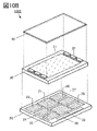
- transistor
- insulator
- Prior art date
- Legal status (The legal status is an assumption and is not a legal conclusion. Google has not performed a legal analysis and makes no representation as to the accuracy of the status listed.)
- Ceased
Links
Images
























Classifications
-
- H—ELECTRICITY
- H10—SEMICONDUCTOR DEVICES; ELECTRIC SOLID-STATE DEVICES NOT OTHERWISE PROVIDED FOR
- H10K—ORGANIC ELECTRIC SOLID-STATE DEVICES
- H10K50/00—Organic light-emitting devices
- H10K50/10—OLEDs or polymer light-emitting diodes [PLED]
- H10K50/19—Tandem OLEDs
-
- G—PHYSICS
- G09—EDUCATION; CRYPTOGRAPHY; DISPLAY; ADVERTISING; SEALS
- G09F—DISPLAYING; ADVERTISING; SIGNS; LABELS OR NAME-PLATES; SEALS
- G09F9/00—Indicating arrangements for variable information in which the information is built-up on a support by selection or combination of individual elements
-
- G—PHYSICS
- G09—EDUCATION; CRYPTOGRAPHY; DISPLAY; ADVERTISING; SEALS
- G09F—DISPLAYING; ADVERTISING; SIGNS; LABELS OR NAME-PLATES; SEALS
- G09F9/00—Indicating arrangements for variable information in which the information is built-up on a support by selection or combination of individual elements
- G09F9/30—Indicating arrangements for variable information in which the information is built-up on a support by selection or combination of individual elements in which the desired character or characters are formed by combining individual elements
-
- G—PHYSICS
- G09—EDUCATION; CRYPTOGRAPHY; DISPLAY; ADVERTISING; SEALS
- G09F—DISPLAYING; ADVERTISING; SIGNS; LABELS OR NAME-PLATES; SEALS
- G09F9/00—Indicating arrangements for variable information in which the information is built-up on a support by selection or combination of individual elements
- G09F9/30—Indicating arrangements for variable information in which the information is built-up on a support by selection or combination of individual elements in which the desired character or characters are formed by combining individual elements
- G09F9/33—Indicating arrangements for variable information in which the information is built-up on a support by selection or combination of individual elements in which the desired character or characters are formed by combining individual elements being semiconductor devices, e.g. diodes
- G09F9/335—Indicating arrangements for variable information in which the information is built-up on a support by selection or combination of individual elements in which the desired character or characters are formed by combining individual elements being semiconductor devices, e.g. diodes being organic light emitting diodes [OLED]
-
- G—PHYSICS
- G09—EDUCATION; CRYPTOGRAPHY; DISPLAY; ADVERTISING; SEALS
- G09G—ARRANGEMENTS OR CIRCUITS FOR CONTROL OF INDICATING DEVICES USING STATIC MEANS TO PRESENT VARIABLE INFORMATION
- G09G3/00—Control arrangements or circuits, of interest only in connection with visual indicators other than cathode-ray tubes
- G09G3/20—Control arrangements or circuits, of interest only in connection with visual indicators other than cathode-ray tubes for presentation of an assembly of a number of characters, e.g. a page, by composing the assembly by combination of individual elements arranged in a matrix no fixed position being assigned to or needed to be assigned to the individual characters or partial characters
-
- G—PHYSICS
- G09—EDUCATION; CRYPTOGRAPHY; DISPLAY; ADVERTISING; SEALS
- G09G—ARRANGEMENTS OR CIRCUITS FOR CONTROL OF INDICATING DEVICES USING STATIC MEANS TO PRESENT VARIABLE INFORMATION
- G09G3/00—Control arrangements or circuits, of interest only in connection with visual indicators other than cathode-ray tubes
- G09G3/20—Control arrangements or circuits, of interest only in connection with visual indicators other than cathode-ray tubes for presentation of an assembly of a number of characters, e.g. a page, by composing the assembly by combination of individual elements arranged in a matrix no fixed position being assigned to or needed to be assigned to the individual characters or partial characters
- G09G3/22—Control arrangements or circuits, of interest only in connection with visual indicators other than cathode-ray tubes for presentation of an assembly of a number of characters, e.g. a page, by composing the assembly by combination of individual elements arranged in a matrix no fixed position being assigned to or needed to be assigned to the individual characters or partial characters using controlled light sources
- G09G3/30—Control arrangements or circuits, of interest only in connection with visual indicators other than cathode-ray tubes for presentation of an assembly of a number of characters, e.g. a page, by composing the assembly by combination of individual elements arranged in a matrix no fixed position being assigned to or needed to be assigned to the individual characters or partial characters using controlled light sources using electroluminescent panels
- G09G3/32—Control arrangements or circuits, of interest only in connection with visual indicators other than cathode-ray tubes for presentation of an assembly of a number of characters, e.g. a page, by composing the assembly by combination of individual elements arranged in a matrix no fixed position being assigned to or needed to be assigned to the individual characters or partial characters using controlled light sources using electroluminescent panels semiconductive, e.g. using light-emitting diodes [LED]
- G09G3/3208—Control arrangements or circuits, of interest only in connection with visual indicators other than cathode-ray tubes for presentation of an assembly of a number of characters, e.g. a page, by composing the assembly by combination of individual elements arranged in a matrix no fixed position being assigned to or needed to be assigned to the individual characters or partial characters using controlled light sources using electroluminescent panels semiconductive, e.g. using light-emitting diodes [LED] organic, e.g. using organic light-emitting diodes [OLED]
- G09G3/3225—Control arrangements or circuits, of interest only in connection with visual indicators other than cathode-ray tubes for presentation of an assembly of a number of characters, e.g. a page, by composing the assembly by combination of individual elements arranged in a matrix no fixed position being assigned to or needed to be assigned to the individual characters or partial characters using controlled light sources using electroluminescent panels semiconductive, e.g. using light-emitting diodes [LED] organic, e.g. using organic light-emitting diodes [OLED] using an active matrix
-
- H—ELECTRICITY
- H05—ELECTRIC TECHNIQUES NOT OTHERWISE PROVIDED FOR
- H05B—ELECTRIC HEATING; ELECTRIC LIGHT SOURCES NOT OTHERWISE PROVIDED FOR; CIRCUIT ARRANGEMENTS FOR ELECTRIC LIGHT SOURCES, IN GENERAL
- H05B33/00—Electroluminescent light sources
- H05B33/02—Details
-
- H—ELECTRICITY
- H05—ELECTRIC TECHNIQUES NOT OTHERWISE PROVIDED FOR
- H05B—ELECTRIC HEATING; ELECTRIC LIGHT SOURCES NOT OTHERWISE PROVIDED FOR; CIRCUIT ARRANGEMENTS FOR ELECTRIC LIGHT SOURCES, IN GENERAL
- H05B33/00—Electroluminescent light sources
- H05B33/12—Light sources with substantially two-dimensional [2D] radiating surfaces
-
- H—ELECTRICITY
- H10—SEMICONDUCTOR DEVICES; ELECTRIC SOLID-STATE DEVICES NOT OTHERWISE PROVIDED FOR
- H10B—ELECTRONIC MEMORY DEVICES
- H10B12/00—Dynamic random access memory [DRAM] devices
-
- H—ELECTRICITY
- H10—SEMICONDUCTOR DEVICES; ELECTRIC SOLID-STATE DEVICES NOT OTHERWISE PROVIDED FOR
- H10B—ELECTRONIC MEMORY DEVICES
- H10B41/00—Electrically erasable-and-programmable ROM [EEPROM] devices comprising floating gates
- H10B41/70—Electrically erasable-and-programmable ROM [EEPROM] devices comprising floating gates the floating gate being an electrode shared by two or more components
-
- H—ELECTRICITY
- H10—SEMICONDUCTOR DEVICES; ELECTRIC SOLID-STATE DEVICES NOT OTHERWISE PROVIDED FOR
- H10B—ELECTRONIC MEMORY DEVICES
- H10B80/00—Assemblies of multiple devices comprising at least one memory device covered by this subclass
-
- H—ELECTRICITY
- H10—SEMICONDUCTOR DEVICES; ELECTRIC SOLID-STATE DEVICES NOT OTHERWISE PROVIDED FOR
- H10D—INORGANIC ELECTRIC SEMICONDUCTOR DEVICES
- H10D30/00—Field-effect transistors [FET]
- H10D30/01—Manufacture or treatment
- H10D30/021—Manufacture or treatment of FETs having insulated gates [IGFET]
-
- H—ELECTRICITY
- H10—SEMICONDUCTOR DEVICES; ELECTRIC SOLID-STATE DEVICES NOT OTHERWISE PROVIDED FOR
- H10D—INORGANIC ELECTRIC SEMICONDUCTOR DEVICES
- H10D30/00—Field-effect transistors [FET]
- H10D30/60—Insulated-gate field-effect transistors [IGFET]
- H10D30/67—Thin-film transistors [TFT]
-
- H—ELECTRICITY
- H10—SEMICONDUCTOR DEVICES; ELECTRIC SOLID-STATE DEVICES NOT OTHERWISE PROVIDED FOR
- H10D—INORGANIC ELECTRIC SEMICONDUCTOR DEVICES
- H10D30/00—Field-effect transistors [FET]
- H10D30/60—Insulated-gate field-effect transistors [IGFET]
- H10D30/68—Floating-gate IGFETs
-
- H—ELECTRICITY
- H10—SEMICONDUCTOR DEVICES; ELECTRIC SOLID-STATE DEVICES NOT OTHERWISE PROVIDED FOR
- H10D—INORGANIC ELECTRIC SEMICONDUCTOR DEVICES
- H10D30/00—Field-effect transistors [FET]
- H10D30/60—Insulated-gate field-effect transistors [IGFET]
- H10D30/69—IGFETs having charge trapping gate insulators, e.g. MNOS transistors
-
- H—ELECTRICITY
- H10—SEMICONDUCTOR DEVICES; ELECTRIC SOLID-STATE DEVICES NOT OTHERWISE PROVIDED FOR
- H10D—INORGANIC ELECTRIC SEMICONDUCTOR DEVICES
- H10D84/00—Integrated devices formed in or on semiconductor substrates that comprise only semiconducting layers, e.g. on Si wafers or on GaAs-on-Si wafers
-
- H—ELECTRICITY
- H10—SEMICONDUCTOR DEVICES; ELECTRIC SOLID-STATE DEVICES NOT OTHERWISE PROVIDED FOR
- H10D—INORGANIC ELECTRIC SEMICONDUCTOR DEVICES
- H10D84/00—Integrated devices formed in or on semiconductor substrates that comprise only semiconducting layers, e.g. on Si wafers or on GaAs-on-Si wafers
- H10D84/01—Manufacture or treatment
- H10D84/0123—Integrating together multiple components covered by H10D12/00 or H10D30/00, e.g. integrating multiple IGBTs
- H10D84/0126—Integrating together multiple components covered by H10D12/00 or H10D30/00, e.g. integrating multiple IGBTs the components including insulated gates, e.g. IGFETs
-
- H—ELECTRICITY
- H10—SEMICONDUCTOR DEVICES; ELECTRIC SOLID-STATE DEVICES NOT OTHERWISE PROVIDED FOR
- H10D—INORGANIC ELECTRIC SEMICONDUCTOR DEVICES
- H10D84/00—Integrated devices formed in or on semiconductor substrates that comprise only semiconducting layers, e.g. on Si wafers or on GaAs-on-Si wafers
- H10D84/01—Manufacture or treatment
- H10D84/02—Manufacture or treatment characterised by using material-based technologies
- H10D84/03—Manufacture or treatment characterised by using material-based technologies using Group IV technology, e.g. silicon technology or silicon-carbide [SiC] technology
- H10D84/038—Manufacture or treatment characterised by using material-based technologies using Group IV technology, e.g. silicon technology or silicon-carbide [SiC] technology using silicon technology, e.g. SiGe
-
- H—ELECTRICITY
- H10—SEMICONDUCTOR DEVICES; ELECTRIC SOLID-STATE DEVICES NOT OTHERWISE PROVIDED FOR
- H10D—INORGANIC ELECTRIC SEMICONDUCTOR DEVICES
- H10D99/00—Subject matter not provided for in other groups of this subclass
-
- H—ELECTRICITY
- H10—SEMICONDUCTOR DEVICES; ELECTRIC SOLID-STATE DEVICES NOT OTHERWISE PROVIDED FOR
- H10K—ORGANIC ELECTRIC SOLID-STATE DEVICES
- H10K50/00—Organic light-emitting devices
-
- H—ELECTRICITY
- H10—SEMICONDUCTOR DEVICES; ELECTRIC SOLID-STATE DEVICES NOT OTHERWISE PROVIDED FOR
- H10K—ORGANIC ELECTRIC SOLID-STATE DEVICES
- H10K59/00—Integrated devices, or assemblies of multiple devices, comprising at least one organic light-emitting element covered by group H10K50/00
-
- H—ELECTRICITY
- H10—SEMICONDUCTOR DEVICES; ELECTRIC SOLID-STATE DEVICES NOT OTHERWISE PROVIDED FOR
- H10K—ORGANIC ELECTRIC SOLID-STATE DEVICES
- H10K59/00—Integrated devices, or assemblies of multiple devices, comprising at least one organic light-emitting element covered by group H10K50/00
- H10K59/10—OLED displays
- H10K59/12—Active-matrix OLED [AMOLED] displays
- H10K59/121—Active-matrix OLED [AMOLED] displays characterised by the geometry or disposition of pixel elements
- H10K59/1213—Active-matrix OLED [AMOLED] displays characterised by the geometry or disposition of pixel elements the pixel elements being TFTs
-
- H—ELECTRICITY
- H10—SEMICONDUCTOR DEVICES; ELECTRIC SOLID-STATE DEVICES NOT OTHERWISE PROVIDED FOR
- H10K—ORGANIC ELECTRIC SOLID-STATE DEVICES
- H10K59/00—Integrated devices, or assemblies of multiple devices, comprising at least one organic light-emitting element covered by group H10K50/00
- H10K59/10—OLED displays
- H10K59/12—Active-matrix OLED [AMOLED] displays
- H10K59/131—Interconnections, e.g. wiring lines or terminals
-
- H—ELECTRICITY
- H10—SEMICONDUCTOR DEVICES; ELECTRIC SOLID-STATE DEVICES NOT OTHERWISE PROVIDED FOR
- H10K—ORGANIC ELECTRIC SOLID-STATE DEVICES
- H10K59/00—Integrated devices, or assemblies of multiple devices, comprising at least one organic light-emitting element covered by group H10K50/00
- H10K59/30—Devices specially adapted for multicolour light emission
- H10K59/32—Stacked devices having two or more layers, each emitting at different wavelengths
-
- G—PHYSICS
- G09—EDUCATION; CRYPTOGRAPHY; DISPLAY; ADVERTISING; SEALS
- G09G—ARRANGEMENTS OR CIRCUITS FOR CONTROL OF INDICATING DEVICES USING STATIC MEANS TO PRESENT VARIABLE INFORMATION
- G09G2320/00—Control of display operating conditions
- G09G2320/06—Adjustment of display parameters
- G09G2320/0626—Adjustment of display parameters for control of overall brightness
-
- H—ELECTRICITY
- H10—SEMICONDUCTOR DEVICES; ELECTRIC SOLID-STATE DEVICES NOT OTHERWISE PROVIDED FOR
- H10K—ORGANIC ELECTRIC SOLID-STATE DEVICES
- H10K59/00—Integrated devices, or assemblies of multiple devices, comprising at least one organic light-emitting element covered by group H10K50/00
- H10K59/80—Constructional details
- H10K59/87—Passivation; Containers; Encapsulations
- H10K59/873—Encapsulations
-
- H—ELECTRICITY
- H10—SEMICONDUCTOR DEVICES; ELECTRIC SOLID-STATE DEVICES NOT OTHERWISE PROVIDED FOR
- H10K—ORGANIC ELECTRIC SOLID-STATE DEVICES
- H10K59/00—Integrated devices, or assemblies of multiple devices, comprising at least one organic light-emitting element covered by group H10K50/00
- H10K59/80—Constructional details
- H10K59/875—Arrangements for extracting light from the devices
- H10K59/876—Arrangements for extracting light from the devices comprising a resonant cavity structure, e.g. Bragg reflector pair
Definitions
- One embodiment of the present invention relates to a semiconductor device.
- one embodiment of the present invention is not limited to the above technical field.
- Technical fields of one embodiment of the present invention disclosed in this specification and the like include semiconductor devices, display devices, light-emitting devices, power storage devices, memory devices, electronic devices, lighting devices, input devices, input/output devices, and driving methods thereof. , or their manufacturing methods, can be mentioned as an example.
- Display devices used in these devices are required to be small in size as well as to have high definition.
- VR, AR, SR, and MR are collectively referred to as xR.
- Display devices for xR include light-emitting devices including light-emitting elements such as organic EL (Electro Luminescence) elements or light-emitting diodes (LEDs), liquid crystal display devices, and the like.
- the basic structure of an organic EL device is to sandwich a layer containing a light-emitting organic compound between a pair of electrodes. By applying a voltage to this device, light can be obtained from the light-emitting organic compound.
- a display device to which such an organic EL element is applied does not require a backlight, which is required in a liquid crystal display device or the like.
- Patent Document 1 describes an example of a display device using an organic EL element.
- Display devices for xR are required to be smaller, consume less power, and have more functions.
- An object of one embodiment of the present invention is to provide a miniaturized display device.
- An object of one embodiment of the present invention is to provide a display device with high color reproducibility.
- An object of one embodiment of the present invention is to provide a high-definition display device.
- An object of one embodiment of the present invention is to provide a display device with high emission luminance.
- An object of one embodiment of the present invention is to provide a highly reliable display device.
- An object of one embodiment of the present invention is to provide a novel display device.
- One aspect of the present invention comprises a first layer, a second layer on the first layer, and a third layer on the second layer, wherein the first layer includes a functional circuit including a first transistor.
- the second layer comprises a plurality of pixel circuits including a second transistor
- the third layer comprises a plurality of light emitting elements, one of the plurality of pixel circuits electrically connected to one of the plurality of light emitting elements
- a functional circuit is a semiconductor device having a function of controlling the operation of a pixel circuit
- a pixel circuit is a semiconductor device having a function of controlling light emission luminance of a light emitting element.
- Si transistors may be used as the first transistor and the second transistor.
- the first layer and the second layer may comprise regions that connect with a Cu--Cu bond.
- an OS transistor may be used as the second transistor.
- Another aspect of the present invention comprises a first layer, a second layer on the first layer, and a first member on the second layer, wherein the first layer comprises a functional circuit;
- the two layers comprise a display section including a plurality of pixels and a plurality of storage sections, each of the plurality of pixels comprising a pixel circuit and a light emitting element on the pixel circuit, the plurality of storage sections comprising:
- the semiconductor device is arranged along at least a part of the outer circumference of the display section, and the display section and the plurality of storage sections are covered with a first member.
- the storage section is arranged in the sealing region.
- the third layer may be translucent.
- One embodiment of the present invention includes a first layer, a second layer over the first layer, and a third layer over the second layer, the first layer including a plurality of memory cells.
- a second layer comprising a functional circuit;
- a third layer comprising a display section including a plurality of pixels;
- the functional circuit comprising a storage section driving circuit and a display section driving circuit; is a semiconductor device including a pixel circuit and a light-emitting element on the pixel circuit.
- the memory cell has a first transistor
- the functional circuit has a second transistor
- the pixel circuit has a third transistor.
- the composition of the first semiconductor layer included in the first transistor and the composition of the second semiconductor layer included in the second transistor may differ from the composition of the third semiconductor layer included in the third transistor.
- the storage section may include a DRAM.
- the above light-emitting device may be an organic EL device.
- the light emitting elements may have a tandem structure.
- the diagonal size of the region containing the plurality of pixel circuits and the plurality of light emitting elements is preferably 0.5 inches or more and 2.0 inches or less. In other words, the diagonal size of the display section is preferably 0.5 inches or more and 2.0 inches or less.
- the functional circuit may include at least one of a CPU, GPU, super-resolution circuit, sensor circuit, communication circuit, or input/output circuit.
- the first member may be translucent.
- a miniaturized display device can be provided.
- a display device with high color reproducibility can be provided.
- a high-definition display device can be provided.
- a display device with high emission luminance can be provided.
- a highly reliable display device can be provided.
- a novel display device can be provided.
- FIG. 1A is a perspective view illustrating a configuration example of a semiconductor device.
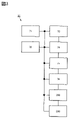
- FIG. 1B is a block diagram of a semiconductor device.
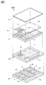
- FIG. 2 is a perspective view illustrating a configuration example of a semiconductor device.
- FIG. 3 is a block diagram for explaining a configuration example of a display drive circuit.
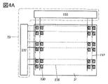
- 4A and FIGS. 4B1 to 4B6 are diagrams illustrating configuration examples of the display unit.
- 5A and 5B are diagrams for explaining a configuration example of a semiconductor device.
- 6A and 6B are diagrams for explaining a configuration example of a semiconductor device.
- FIG. 7 is a perspective view illustrating a configuration example of a semiconductor device.
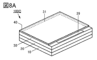
- 8A and 8B are perspective views illustrating configuration examples of semiconductor devices.
- FIG. 9A and 9B are perspective views illustrating configuration examples of the semiconductor device.
- 10A and 10B are perspective views illustrating configuration examples of semiconductor devices.
- 11A and 11B are perspective views illustrating configuration examples of semiconductor devices.
- 12A and 12B are perspective views illustrating configuration examples of semiconductor devices.
- 13A and 13B are perspective views illustrating configuration examples of semiconductor devices.
- 14A and 14B are perspective views illustrating configuration examples of semiconductor devices.
- 15A and 15B are diagrams for explaining a configuration example of a semiconductor device.
- 16A and 16B are diagrams illustrating a configuration example of a semiconductor device.
- 17A to 17C are diagrams illustrating operation examples of the semiconductor device.
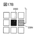
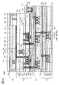
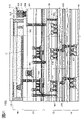
- FIG. 18 is a cross-sectional view showing a configuration example of a semiconductor device.
- FIG. 18 is a cross-sectional view showing a configuration example of a semiconductor device.
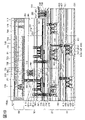
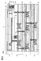
- FIG. 19 is a cross-sectional view showing a configuration example of a semiconductor device.
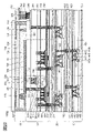
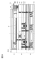
- FIG. 20 is a cross-sectional view showing a configuration example of a semiconductor device.
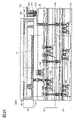
- FIG. 21 is a cross-sectional view showing a configuration example of a semiconductor device.
- FIG. 22 is a cross-sectional view showing a configuration example of a semiconductor device.
- FIG. 23 is a cross-sectional view showing a configuration example of a semiconductor device.
- FIG. 24 is a cross-sectional view showing a configuration example of a semiconductor device.
- FIG. 25 is a cross-sectional view showing a configuration example of a semiconductor device.
- FIG. 26 is a cross-sectional view showing a configuration example of a semiconductor device.
- FIG. 20 is a cross-sectional view showing a configuration example of a semiconductor device.
- FIG. 21 is a cross-sectional view showing a configuration example of a semiconductor device.
- FIG. 22 is a cross-sectional view showing a
- FIG. 27 is a cross-sectional view showing a configuration example of a semiconductor device.
- FIG. 28 is a cross-sectional view showing a configuration example of a semiconductor device.
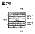
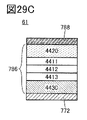
- 29A to 29D are diagrams illustrating configuration examples of light-emitting elements.
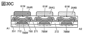
- 30A to 30D are diagrams showing configuration examples of display devices.
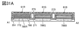
- 31A to 31D are diagrams showing configuration examples of display devices.
- FIG. 32A is a top view showing a configuration example of a transistor.
- 32B and 32C are cross-sectional views showing configuration examples of transistors.
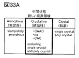
- FIG. 33A is a diagram explaining the classification of crystal structures.
- FIG. 33B is a diagram explaining the XRD spectrum of the CAAC-IGZO film.
- FIG. 33C is a diagram illustrating an ultrafine electron diffraction pattern of a CAAC-IGZO film.
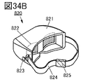
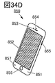
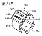
- 34A to 34E are diagrams illustrating examples of electronic devices.
- a semiconductor device is a device that utilizes semiconductor characteristics and refers to a circuit including a semiconductor element (transistor, diode, photodiode, or the like), a device having the same circuit, and the like. It also refers to all devices that can function by utilizing semiconductor characteristics. For example, an integrated circuit, a chip with an integrated circuit, and an electronic component containing a chip in a package are examples of semiconductor devices. Storage devices, display devices, light-emitting devices, lighting devices, electronic devices, and the like are themselves semiconductor devices and may include semiconductor devices.
- connection relationships other than the connection relationships shown in the drawings or the text are not limited to the predetermined connection relationships, for example, the connection relationships shown in the drawings or the text. It is assumed that X and Y are objects (for example, devices, elements, circuits, wiring, electrodes, terminals, conductive films, layers, etc.).
- X and Y are electrically connected is an element that enables electrical connection between X and Y (for example, switch, transistor, capacitive element, inductor, resistive element, diode, display devices, light emitting devices, loads, etc.) can be connected between X and Y.
- the switch is controlled to be on and off. In other words, the switch has a function of controlling whether it is in a conducting state (on state) or a non-conducting state (off state) to allow current to flow.
- a circuit that enables functional connection between X and Y eg, a logic circuit (inverter, NAND circuit, NOR circuit, etc.), a signal conversion Circuits (digital-to-analog conversion circuit, analog-to-digital conversion circuit, gamma correction circuit, etc.), potential level conversion circuit (power supply circuit (booster circuit, step-down circuit, etc.), level shifter circuit that changes the potential level of signals, etc.), voltage source, current source , switching circuit, amplifier circuit (circuit that can increase signal amplitude or current amount, operational amplifier, differential amplifier circuit, source follower circuit, buffer circuit, etc.), signal generation circuit, memory circuit, control circuit, etc.) It is possible to connect one or more between As an example, even if another circuit is interposed between X and Y, when a signal output from X is transmitted to Y, X and Y are considered to be functionally connected. do.
- X and Y are electrically connected, it means that X and Y are electrically connected (that is, another element or another circuit is interposed), and the case where X and Y are directly connected (that is, the case where X and Y are connected without another element or another circuit between them). (if any).
- X and Y, the source (or the first terminal, etc.) and the drain (or the second terminal, etc.) of the transistor are electrically connected to each other, and X, the source of the transistor (or the 1 terminal, etc.), the drain of the transistor (or the second terminal, etc.), and are electrically connected in the order of Y.”
- the source (or first terminal, etc.) of the transistor is electrically connected to X
- the drain (or second terminal, etc.) of the transistor is electrically connected to Y
- X is the source of the transistor ( or the first terminal, etc.), the drain of the transistor (or the second terminal, etc.), and Y are electrically connected in this order.
- X is electrically connected to Y through the source (or first terminal, etc.) and drain (or second terminal, etc.) of the transistor, and X is the source (or first terminal, etc.) of the transistor; terminal, etc.), the drain of the transistor (or the second terminal, etc.), and Y are provided in this connection order.
- the source (or the first terminal, etc.) and the drain (or the second terminal, etc.) of the transistor can be distinguished by defining the order of connection in the circuit configuration.
- the technical scope can be determined.
- these expression methods are examples, and are not limited to these expression methods.
- X and Y are objects (for example, devices, elements, circuits, wiring, electrodes, terminals, conductive films, layers, etc.).
- circuit diagram shows independent components electrically connected to each other, if one component has the functions of multiple components.
- one component has the functions of multiple components.
- the term "electrically connected" in this specification includes cases where one conductive film functions as a plurality of constituent elements.
- the term “capacitance element” refers to, for example, a circuit element having a capacitance value higher than 0 F, a wiring region having a capacitance value higher than 0 F, a parasitic capacitance, a transistor can be the gate capacitance of Therefore, in this specification and the like, the term “capacitance element” means not only a circuit element including a pair of electrodes and a dielectric material contained between the electrodes, but also a parasitic element occurring between wirings. Capacitance, gate capacitance generated between one of the source or drain of the transistor and the gate, and the like are included.
- capacitor element in addition, terms such as “capacitance element”, “parasitic capacitance”, and “gate capacitance” can be replaced with terms such as “capacitance”, and conversely, the term “capacitance” can be replaced with terms such as “capacitance element”, “parasitic capacitance”, and “capacitance”. term such as “gate capacitance”.
- a pair of electrodes” in the “capacitance” can be replaced with a "pair of conductors," a “pair of conductive regions,” a “pair of regions,” and the like.
- the value of the capacitance can be, for example, 0.05 fF or more and 10 pF or less. Also, for example, it may be 1 pF or more and 10 ⁇ F or less.
- a transistor has three terminals called a gate, a source, and a drain.
- a gate is a control terminal that controls the conduction state of a transistor.
- the two terminals functioning as source or drain are the input and output terminals of the transistor.
- One of the two input/output terminals functions as a source and the other as a drain, depending on the conductivity type of the transistor (n-channel type, p-channel type) and the level of potentials applied to the three terminals of the transistor. Therefore, in this specification and the like, the terms “source” and “drain” can be used interchangeably.
- a transistor may have a back gate in addition to the three terminals described above, depending on the structure of the transistor.
- one of the gate and back gate of the transistor may be referred to as a first gate
- the other of the gate and back gate of the transistor may be referred to as a second gate.
- the terms "gate” and “backgate” may be used interchangeably for the same transistor.
- the respective gates may be referred to as a first gate, a second gate, a third gate, or the like in this specification and the like.
- a “node” can be replaced with a terminal, a wiring, an electrode, a conductive layer, a conductor, an impurity region, or the like, depending on the circuit configuration, device structure, and the like. Also, terminals, wirings, etc. can be rephrased as “nodes”.
- ordinal numbers such as “first”, “second”, and “third” are added to avoid confusion of constituent elements. Therefore, the number of components is not limited. Also, the order of the components is not limited. For example, a component referred to as “first” in one embodiment such as this specification is a component referred to as “second” in other embodiments or claims. It is possible. Further, for example, a component referred to as “first” in one of the embodiments in this specification may be omitted in other embodiments or the scope of claims.
- electrode B on insulating layer A does not require that electrode B be formed on insulating layer A in direct contact with another configuration between insulating layer A and electrode B. Do not exclude those containing elements.
- terms such as “film” and “layer” can be interchanged depending on the situation.
- the terms “film”, “layer”, etc. can be omitted and replaced with other terms.
- the terms “insulating layer” and “insulating film” may be changed to the term “insulator”.
- Electrode any electrode that is used as part of a “wiring” and vice versa.
- the term “electrode” or “wiring” includes the case where a plurality of “electrodes” or “wiring” are integrally formed.
- terminal may be used as part of “wiring” or “electrode” and vice versa.
- terminal includes a case where a plurality of "electrodes", “wirings”, “terminals”, etc. are integrally formed.
- an “electrode” can be part of a “wiring” or a “terminal”, and a “terminal” can be part of a “wiring” or an “electrode”, for example.
- Terms such as “electrode”, “wiring”, and “terminal” may be replaced with terms such as "region” in some cases.
- terms such as “wiring”, “signal line”, and “power line” can be interchanged depending on the case or situation. For example, it may be possible to change the term “wiring” to the term “signal line”. Also, for example, it may be possible to change the term “wiring” to a term such as "power supply line”. Also, vice versa, terms such as “signal line” and “power line” may be changed to the term “wiring”. It may be possible to change terms such as “power line” to terms such as “signal line”. Also, vice versa, terms such as “signal line” may be changed to terms such as "power line”. In addition, the term “potential” applied to the wiring may be changed to the term “signal” depending on the circumstances. And vice versa, terms such as “signal” may be changed to the term “potential”.
- parallel means a state in which two straight lines are arranged at an angle of -10° or more and 10° or less. Therefore, the case of ⁇ 5° or more and 5° or less is also included.
- substantially parallel or “substantially parallel” refers to a state in which two straight lines are arranged at an angle of -30° or more and 30° or less.
- Perfect means that two straight lines are arranged at an angle of 80° or more and 100° or less. Therefore, the case of 85° or more and 95° or less is also included.
- FIG. 1A and 2 are perspective views of a semiconductor device 100A according to one embodiment of the present invention.
- FIG. 1B is a block diagram illustrating the configuration of the semiconductor device 100A.
- the semiconductor device 100A includes a layer 20 on the layer 10 , a layer 30 on the layer 20 , and a sealing substrate 40 on the layer 30 .
- the layer 30 also includes a plurality of pixel circuits 51 , and a layer 60 is provided between the sealing substrate 40 and the plurality of pixel circuits 51 .
- the layers 10, 20, 30, 60, the sealing substrate 40, and the like are shown separately in order to make the configuration of the semiconductor device 100A easier to understand.
- Layer 10 comprises storage unit 11 .
- the storage unit 11 also includes a plurality of memory cells 12 .
- the memory cell 12 functions as a storage element.
- storage devices of various storage methods can be used. For example, DRAM (Dynamic Random Access Memory), SRAM (Static Random Access Memory), phase change memory (PCM: Phase-Change Memory), resistance change memory (ReRAM: Resistive Random Access Memory), magnetoresistive memory (MRAM: Memory Random Access Memory), ferroelectric memory (FeRAM: Ferroelectric Random Access Memory), antiferroelectric memory (Antiferroelectric Memory), etc. may be used.
- NOSRAM Nonvolite Oxide Semiconductor Random Access Memory
- DOSRAM Dynamic Oxide Semiconductor Random Access Memory
- OS transistor a transistor including an oxide semiconductor in a channel formation region
- the storage unit 11 may include multiple types of storage devices. For example, a non-volatile storage device and a volatile storage device may be provided.
- the storage unit 11 has a function of holding various programs used in the semiconductor device 100A, data necessary for the operation of the semiconductor device 100A, and the like.
- the Layer 20 comprises functional circuitry 90 and terminals 29 .
- the functional circuit 90 includes a CPU 21 (Central Processing Unit), a GPU 22 (Graphics Processing Unit), a display drive circuit 23, a storage drive circuit 24, a super-resolution circuit 25, a sensor circuit 26, a communication circuit 27, and an input/output circuit 28. Prepare.
- the functional circuit 90 may not include all of these configurations, or may include configurations other than these.
- a potential generation circuit that generates a plurality of different potentials and/or a power management circuit that controls power supply and stop for each circuit included in the semiconductor device 100A may be provided.
- Power supply and stop may be performed for each circuit constituting the CPU 21 .
- power consumption can be reduced by stopping power supply to a circuit that has been determined not to be used for a while among circuits constituting the CPU 21 and restarting power supply when necessary.
- Data necessary for resuming the power supply may be stored in the storage circuit in the CPU 21, the storage unit 11, or the like before the circuit is stopped. By storing the data necessary for circuit recovery, a stopped circuit can be recovered at high speed.
- the circuit operation may be stopped by stopping the supply of the clock signal.
- the functional circuit 90 may also include a DSP (Digital Signal Processor) and/or an FPGA (Field Programmable Gate Array).
- DSP Digital Signal Processor
- FPGA Field Programmable Gate Array
- the CPU 21 has a function of controlling the operations of the circuits provided in the GPU 22 and the layer 20 according to the programs stored in the storage unit 11 .
- the GPU 22 has a function of performing arithmetic processing for forming image data. Also, since the GPU 22 can perform many matrix operations (product-sum operations) in parallel, it is possible to perform, for example, arithmetic processing using a neural network at high speed.
- the GPU 22 has a function of correcting image data using correction data stored in the storage unit 11, for example. For example, the GPU 22 has a function of generating image data with corrected brightness, hue, and/or contrast.
- the display driver circuit 23 is electrically connected to the plurality of pixel circuits 51 included in the layer 30 and has a function of supplying image data to the plurality of pixel circuits 51 .
- Various circuits such as a shift register, a level shifter, an inverter, a latch, an analog switch, or a logic circuit can be used for the display drive circuit 23 .
- a layer 60 is provided over the layer 30 .
- Layer 60 comprises a plurality of light emitting elements 61 .
- One light emitting element 61 and one pixel circuit 51 are electrically connected to function as one pixel.
- the pixel circuit 51 controls the light emission luminance of the light emitting element 61 .
- a display unit 31 is configured by a plurality of pixels. That is, it can be said that the display unit 31 includes a plurality of pixels.
- Layer 30 may also include layer 60 . In this case, it can be said that the layer 30 includes the display section 31 . Note that the pixel circuit 51 and the light emitting element 61 will be described later.
- the super-resolution circuit 25 has a function of determining the potential of an arbitrary pixel included in the display section 31 by performing a product-sum operation of the potentials of the pixels surrounding the pixel and the weight.
- the super-resolution circuit 25 has a function of up-converting image data having a resolution lower than that of the display section 31 .
- the super-resolution circuit 25 also has a function of down-converting image data having a resolution higher than that of the display section 31 .
- the GPU 22 can perform up-conversion or down-conversion of image data, but the load on the GPU 22 can be reduced by providing the super-resolution circuit 25 .
- the GPU 22 performs processing up to 2K resolution (or 4K resolution), and the super-resolution circuit 25 up-converts to 4K resolution (or 8K resolution), thereby reducing the load on the GPU 22 .
- the processing speed of the semiconductor device 100A can be increased.
- the memory driving circuit 24 is electrically connected to the memory 11 included in the layer 10 and has a function of writing data to the memory 11 and a function of reading data from the memory 11 .
- the sensor circuit 26 has a function of acquiring any one or more of human visual, auditory, tactile, gustatory, and olfactory information. More specifically, the sensor circuit 26 detects force, displacement, position, velocity, acceleration, angular velocity, number of revolutions, distance, light, magnetism, temperature, sound, time, electric field, current, voltage, power, radiation, humidity, It has at least one of the functions of detecting or measuring tilt, vibration, smell, and infrared rays. Also, the sensor circuit 26 may have functions other than these.
- the communication circuit 27 has a function of communicating wirelessly or by wire.
- having a function of wireless communication is preferable because the number of components such as cables for connection can be omitted.
- the communication circuit 27 When the communication circuit 27 has a function of communicating wirelessly, the communication circuit 27 can communicate via an antenna.
- LTE Long Term Evolution
- GSM Global System for Mobile Communication: registered trademark
- EDGE Enhanced Data Rates for GSM Evolution
- CDMA2000 Code Division 0 Multiplication
- IEEE specifications standardized by IEEE such as Wi-Fi (registered trademark), Bluetooth (registered trademark), and ZigBee (registered trademark).
- the communication circuit 27 includes the Internet, intranet, extranet, PAN (Personal Area Network), LAN (Local Area Network), CAN (Campus Area Network), MAN (Metropolitan Area Network), Information can be input/output by connecting the semiconductor device 100A to other devices via computer networks such as WAN (Wide Area Network) and GAN (Global Area Network).
- PAN Personal Area Network
- LAN Local Area Network
- CAN Campus Area Network
- MAN Metropolitan Area Network
- Information can be input/output by connecting the semiconductor device 100A to other devices via computer networks such as WAN (Wide Area Network) and GAN (Global Area Network).
- the input/output circuit 28 has a function of distributing signals supplied to the semiconductor device 100A via the terminal section 29 to circuits such as the CPU 21 and/or the GPU 22 .
- the input/output circuit 28 also has a function of distributing signals supplied to the semiconductor device 100A via the communication circuit 27 to circuits such as the CPU 21 and/or the GPU 22 .
- the input/output circuit 28 also has a function of outputting a signal to the outside via the terminal section 29 .
- the input/output circuit 28 also has a function of outputting a signal to the outside via the communication circuit 27 .
- FPCs flexible printed circuits
- the layer 30 and the sealing substrate 40 are not formed in the region overlapping the terminal portion 29 .
- FIG. 3 is a block diagram illustrating a configuration example of the display section drive circuit 23.
- the display drive circuit 23 includes a control circuit 71 , a timing controller 72 , a serial/parallel conversion circuit 73 , a latch circuit 74 , a DAC 75 , an amplifier circuit 76 , a first drive circuit 232 and a second drive circuit 233 .
- the display unit drive circuit 23 may not have all of these configurations, or may have configurations other than these.
- the control circuit 71 is electrically connected to the timing controller 72 , the serial/parallel conversion circuit 73 , the latch circuit 74 , the DAC 75 , the amplifier circuit 76 , the first drive circuit 232 and the second drive circuit 233 . It has a function to control the operation. For example, it controls the adjustment of the output characteristics of the DAC 75 and the stopping of the amplifier circuit 76 when the display image is not updated. Further, when the display unit 31 is divided into a plurality of sub-screens and driven, the control circuit 71 has a function of controlling the above operation for each sub-screen. In addition, the control circuit 71 may have a function of controlling, for each sub-screen, conditions for setting weights used by the GPU 22, the super-resolution circuit 25, and the like.
- the timing controller 72 has a function of controlling the timing of updating the display image according to the frame frequency.
- the timing controller 72 has a function of controlling the timing of updating the display image for each sub-screen.
- the serial-to-parallel conversion circuit 73 has a function of sorting the digital image signal input by the serial transmission method to each signal line (for example, wiring 237 described later).
- the distributed digital image signals are temporarily held in the latch circuit 74 and then converted into analog image signals by the DAC 75 .
- the analog image signal is amplified by the amplifier circuit 76 and supplied to the signal line.
- FIG. 4A is a block diagram illustrating the connection relationship between the display section drive circuit 23 and the display section 31. As shown in FIG.
- the display drive circuit 23 has a first drive circuit 232 and a second drive circuit 233 .
- a circuit included in the first driving circuit 232 functions, for example, as a scanning line driving circuit.
- a circuit included in the second drive circuit 233 functions, for example, as a signal line drive circuit. It should be noted that some circuit may be provided at a position facing the first drive circuit 232 with the display section 31 interposed therebetween. Some circuit may be provided at a position facing the second drive circuit 233 with the display section 31 interposed therebetween.
- the display unit drive circuit 23 may be referred to as a "peripheral drive circuit".
- Various circuits such as shift registers, level shifters, inverters, latches, analog switches, and logic circuits can be used for the peripheral driving circuits.
- a transistor, a capacitor, or the like can be used for the peripheral driver circuit.
- the display unit 31 includes m wirings 236 (m is an integer equal to or greater than 1), which are arranged substantially parallel to each other and whose potentials are controlled by circuits included in the first driving circuit 232. and n wirings 237 (n is an integer equal to or greater than 1) that are arranged substantially in parallel and whose potentials are controlled by a circuit included in the second driving circuit 233 .
- the wiring 236 is electrically connected to the first drive circuit 232 .
- the wiring 237 is electrically connected to the second driving circuit 233 .
- the display section 31 has a plurality of pixels 230 arranged in a matrix.
- the pixel 230 that controls red light, the pixel 230 that controls green light, and the pixel 230 that controls blue light are collectively functioned as one pixel 240, and the light emission amount (light emission luminance) of each pixel 230 is controlled. By doing so, full-color display can be realized. Therefore, each of the three pixels 230 functions as a sub-pixel. That is, each of the three sub-pixels controls the amount of red light, green light, or blue light emitted (see FIG. 4B1).
- the color of light controlled by each of the three sub-pixels is not limited to a combination of red (R), green (G), and blue (B), but may be cyan (C), magenta (M), and yellow (Y). There may be (see FIG. 4B2). Also, the areas of the three sub-pixels may not be the same. If the luminous efficiency, reliability, etc. differ depending on the luminescent color, the area of the sub-pixel may be changed for each luminescent color (see FIG. 4B3). Note that the arrangement configuration of the sub-pixels shown in FIG. 4B3 may be referred to as "S stripe arrangement".
- four sub-pixels may be collectively functioned as one pixel.
- a sub-pixel controlling white light may be added to three sub-pixels controlling red light, green light, and blue light, respectively (see FIG. 4B4).
- a sub-pixel for controlling yellow light may be added to the three sub-pixels for controlling red light, green light, and blue light (see FIG. 4B5).
- a sub-pixel for controlling white light may be added to the three sub-pixels for controlling cyan, magenta, and yellow light, respectively (see FIG. 4B6).
- Reproducibility of halftones can be improved by increasing the number of sub-pixels that function as one pixel, and by appropriately combining sub-pixels that control lights such as red, green, blue, cyan, magenta, and yellow. can. Therefore, color reproducibility can be improved.
- the display device of one embodiment of the present invention can reproduce color gamuts of various standards.
- the PAL Phase Alternating Line
- NTSC National Television System Committee
- sRGB standard RGB
- Adobe RGB ITU-R BT. 709(International Telecommunication Union Radiocommunication Sector Broadcasting Service(Television) 709) ⁇ DCI ⁇ P3(Digital Cinema Initiatives P3) ⁇ UHDTV(Ultra High Definition Television ⁇ ) ⁇ ITU ⁇ RBT. 2020 (REC.2020 (Recommendation 2020)) standard color gamut can be reproduced.
- the display unit 31 capable of full-color display at a so-called full high-definition resolution (also called “2K resolution”, “2K1K”, or “2K”) is realized.
- the display unit 31 is capable of full-color display at a resolution of so-called ultra-high-definition (also referred to as “4K resolution”, “4K2K”, or “4K”).
- 4K resolution also referred to as “4K resolution”, “4K2K”, or “4K”.
- the display unit 31 is capable of full-color display at a resolution of so-called Super Hi-Vision (also referred to as “8K resolution”, “8K4K”, or “8K”). can be realized.
- Super Hi-Vision also referred to as “8K resolution”, “8K4K”, or “8K”.
- the pixel density (definition) of the display section 31 is preferably 1000 ppi or more and 10000 ppi or less.
- it may be 2000 ppi or more and 6000 ppi or less, or 3000 ppi or more and 5000 ppi or less.
- the screen ratio (aspect ratio) of the display unit 31 is not particularly limited.
- the display unit 31 of the semiconductor device 100A can support various screen ratios such as 1:1 (square), 4:3, 16:9, and 16:10.
- the diagonal size of the display section 31 is 0.1 inch or more and 5.0 inches or less, preferably 0.5 inch or more and 2.0 inches or less, more preferably. can be greater than or equal to 1 inch and less than or equal to 1.7 inches.
- the diagonal size of the display section 31 may be 1.5 inches or around 1.5 inches.
- FIG. 5 shows a circuit configuration example of the pixel 230.
- Pixel 230 comprises pixel circuit 51 and light emitting element 61 .
- FIG. 5A is a diagram showing connection of each element included in the pixel 230.
- FIG. 5B is a diagram schematically showing the vertical relationship among the layer 20 including the display drive circuit 23, the layer 30 including the pixel circuit 51, and the layer 60 including the light emitting element 61.
- FIG. 5A is a diagram showing connection of each element included in the pixel 230.
- FIG. 5B is a diagram schematically showing the vertical relationship among the layer 20 including the display drive circuit 23, the layer 30 including the pixel circuit 51, and the layer 60 including the light emitting element 61.
- a pixel circuit 51 shown as an example in FIGS. 5A and 5B includes a transistor 52A, a transistor 52B, a transistor 52C, and a capacitor 53.
- the transistors 52A, 52B, and 52C can be OS transistors.
- Each of the OS transistors of the transistor 52A, the transistor 52B, and the transistor 52C preferably has a back gate electrode. It can be configured to provide a signal.
- the transistor 52B includes a gate electrode electrically connected to the transistor 52A, a first terminal electrically connected to the light emitting element 61, and a second terminal electrically connected to the wiring ANO.
- the wiring ANO is wiring for applying a potential for supplying current to the light emitting element 61 .
- the transistor 52A has a first terminal electrically connected to the gate electrode of the transistor 52B and a second terminal electrically connected to a wiring SL functioning as a source line, and functions as a gate line. It has a function of controlling a conductive state or a non-conductive state based on the potential of the wiring GL1.
- the transistor 52C has a first terminal electrically connected to the wiring V0 and a second terminal electrically connected to the light emitting element 61, and the potential of the wiring GL2 functioning as a gate line is applied to the transistor 52C. , has a function of controlling the conducting state or the non-conducting state.
- the wiring V0 is a wiring for applying a reference potential and a wiring for outputting the current flowing through the pixel circuit 51 to the display section driving circuit 23 .
- the capacitor 53 includes a conductive film electrically connected to the gate electrode of the transistor 52B and a conductive film electrically connected to the second terminal of the transistor 52C.
- the light emitting element 61 includes a first electrode electrically connected to the first terminal of the transistor 52B and a second electrode electrically connected to the wiring VCOM.
- the wiring VCOM is a wiring for applying a potential for supplying current to the light emitting element 61 .
- the intensity of the light emitted by the light emitting element 61 can be controlled according to the image signal applied to the gate electrode of the transistor 52B. Variation in the potential between the gate and source of the transistor 52B can be suppressed by the reference potential of the wiring V0 applied through the transistor 52C.
- a current value that can be used for setting pixel parameters can be output from the wiring V0.
- the wiring V0 can function as a monitor line for outputting the current flowing through the transistor 52B or the current flowing through the light emitting element 61 to the outside.
- the current output to the wiring V0 may be converted into voltage by a source follower circuit or the like.
- a self-luminous display element such as an LED (Light Emitting Diode) or an OLED (Organic Light Emitting Diode. Also referred to as “organic EL element” or “OEL”) can be used.
- a self-luminous light-emitting element such as a micro LED, a QLED (Quantum-dot Light Emitting Diode), or a semiconductor laser may be used.
- the wiring that electrically connects the pixel circuit 51 and the display driver circuit 23 can be shortened, so that the wiring resistance of the wiring can be reduced.
- parasitic capacitance of the wiring can be reduced. Therefore, since data can be written at high speed, the display section 31 can be driven at high speed. As a result, a sufficient frame period can be secured even if the number of pixel circuits 51 is increased, so the pixel density of the display section 31 can be increased.
- the definition of the image displayed on the display section 31 can be increased.
- the pixel density of the display section 31 can be 1000 ppi or more, 5000 ppi or more, or 7000 ppi or more.
- the semiconductor device 100A can be used, for example, as a display device for xR such as AR or VR.
- the semiconductor device 100A according to one embodiment of the present invention can be suitably applied to electronic devices, such as HMDs, in which the distance between the display unit and the user is short.
- FIG. 6A shows a modification of the circuit configuration of the pixel 230 shown in FIG. 5A.
- the circuit configuration shown in FIG. 6A has a configuration obtained by removing the transistor 52C, the wiring GL2, and the wiring V0 from the circuit configuration shown in FIG. 5A.
- a transistor having a back gate may be used as the transistor 52A, and the back gate and the gate may be electrically connected.
- the back gate may be electrically connected to either the source or the drain of the transistor.
- the semiconductor device 100A of one embodiment of the present invention has a structure in which the display portion 31, the functional circuit 90, and the memory portion 11 are stacked.
- the miniaturization of the semiconductor device 100A can be realized.
- the width of the frame around the display 31 can be extremely narrowed, so that the area of the display 31 can be increased. Therefore, the resolution of the display section 31 can be improved. Therefore, the display quality of the semiconductor device 100A can be improved.
- the area occupied by one pixel can be increased. Therefore, the emission brightness of the display section 31 can be increased.
- the aperture ratio of pixels can be increased.
- the pixel aperture ratio can be 40% or more and less than 100%, preferably 50% or more and 95% or less, more preferably 60% or more and 95% or less.
- the current density supplied to the pixel can be reduced. Therefore, the load applied to the pixel is reduced, and the reliability of the semiconductor device 100A can be improved.
- the wiring that electrically connects them can be shortened. Therefore, wiring resistance and parasitic capacitance are reduced, and the operating speed of the semiconductor device 100A can be increased. Also, the power consumption of the semiconductor device 100A is reduced.
- the storage unit 11 is used for temporary storage of a large amount of data used for computation and computation result data.
- the layer 30 including the display portion 31 and the layer 10 including the storage portion 11 sandwich the layer 20 including the functional circuit 90. This is preferable because it is possible to shorten both of the wirings connecting the memory drive circuit 24 .
- the layer 10 is preferably in contact with a material with high thermal conductivity (for example, a metal material such as copper or aluminum).
- a material with high thermal conductivity for example, a metal material such as copper or aluminum.
- FIG. 7 shows a semiconductor device 100B that is a modification of the semiconductor device 100A.
- FIG. 7 is a perspective view of a semiconductor device 100B according to one embodiment of the present invention.
- the layers 10, 20, 30, 60, the sealing substrate 40, and the like are shown separately in order to make the configuration of the semiconductor device 100B easier to understand.
- the semiconductor device 100B differs in the stacking order of the layers 10 and 20 from the semiconductor device 100A. Specifically, semiconductor device 100B includes layer 10 on layer 20 , layer 30 on layer 10 , and sealing substrate 40 on layer 30 . Also, the terminal portion 19 is provided on the layer 10 instead of the terminal portion 29 on the layer 20 . Although not shown, the layer 20 in the semiconductor device 100B is preferably in contact with a radiator. Note that the heat radiator means one having a function of releasing heat generated in the semiconductor device 100B to the outside of the semiconductor device 100B.
- the stacking order of layers can be changed depending on the purpose or application.
- FIG. 8 shows a semiconductor device 100C that is a modification of the semiconductor device 100A.
- 8A and 8B are perspective views of a semiconductor device 100C according to one embodiment of the present invention.
- the layers 10, 20, and 30 are separated to make the configuration of the semiconductor device 100C easier to understand.
- the semiconductor device 100 ⁇ /b>C does not include the terminal section 29 on the layer 20 , and includes the terminal section 39 on the layer 30 instead of the terminal section 29 .
- FIG. 9 shows a semiconductor device 100D that is a modification of the semiconductor device 100A.
- 9A and 9B are perspective views of a semiconductor device 100D according to one embodiment of the present invention.
- the layers 20, 30, and sealing substrate 40 are shown separately in order to make the configuration of the semiconductor device 100D easier to understand.
- the semiconductor device 100 ⁇ /b>D does not include the layer 10 , but instead includes a plurality of memory chips 32 functioning as the storage section 11 on the layer 30 and around the display section 31 .
- a plurality of memory chips 32 are arranged along the outer circumference of the display section 31 .
- memory chips 32 are arranged on three sides of a display section 31, and layers 30 and 20 are electrically connected using a plurality of wires 38 on the remaining one side. Note that the wire 38 may be formed by a wire bonding method.
- memory chips 32 can be mounted to layer 30 using a variety of materials and methods, such as anisotropic conductive adhesives, ball bonding, or wire bonding.
- anisotropic conductive adhesives such as ball bonding, or wire bonding.
- Cu-Cu bonding (a method of ensuring electrical connection by exposing each Cu pad at the bonding interface and contacting both pads) or bonding using a TSV (Through Silicon Via) and a bump to the layer 30 May be implemented.
- the memory chip 32 is preferably arranged at a position overlapping a sealing material 712 (also referred to as a “sealing material”; the sealing material 712 will be described later) that bonds the layer 30 and the sealing substrate 40 together.
- a region where the layer 30, the sealing material 712, and the sealing substrate 40 overlap is also referred to as a "sealing region.”
- the display section 31 and the memory chip 32 are covered with the sealing substrate 40 .
- the sealing substrate 40 By covering the memory chips 32 with the sealing substrate 40 , it is possible to prevent external impurities from diffusing into the memory chips 32 .
- FIG. 10 shows a semiconductor device 100E that is a modification of the semiconductor device 100D.
- 10A and 10B are perspective views of a semiconductor device 100E according to one embodiment of the present invention.
- the layers 20, 30, and sealing substrate 40 are shown separated for easy understanding of the configuration of the semiconductor device 100E. Note that the description of the layer 60 is omitted.
- the semiconductor device 100E has a memory chip 32 arranged on one of the two sides facing each other among the four sides adjacent to the display section 31, and wires 38 electrically connecting the layers 30 and 20 on the other two sides. .
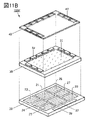
- FIG. 11 shows a semiconductor device 100F that is a modification of the semiconductor device 100D.
- 11A and 11B are perspective views of a semiconductor device 100F according to one embodiment of the present invention.
- the layers 20, 30, the sealing substrate 40, and the like are shown separately in order to make the configuration of the semiconductor device 100F easier to understand. Note that the description of the layer 60 is omitted.
- a sealing substrate 40 included in the semiconductor device 100F includes a plurality of cutouts 42 .
- the notch 42 is provided at a position overlapping the memory chip 32 .
- the sealing substrate 40 and the layer 30 are bonded together so that the memory chip 32 is accommodated in the notch 42 .
- the semiconductor device 100E can be thinner than the semiconductor device 100D.
- FIG. 12 shows a semiconductor device 100G that is a modification of the semiconductor device 100D.
- 12A and 12B are perspective views of a semiconductor device 100G according to one embodiment of the present invention.
- the layers 20, 30, the sealing substrate 40, and the like are shown separately in order to make the configuration of the semiconductor device 100G easier to understand. Note that the description of the layer 60 is omitted.
- the semiconductor device 100G differs from the semiconductor device 100D in that the sealing substrate 40 overlaps the display section 31 and does not overlap the memory chip 32 .
- the thickness of the semiconductor device 100G can be reduced.
- the sealing substrate 40 becomes smaller, the weight of the semiconductor device 100G can be reduced.
- FIG. 13 shows a semiconductor device 100H that is a modification of the semiconductor device 100C.
- 13A and 13B are perspective views of the semiconductor device 100H.
- Semiconductor device 100H differs from semiconductor device 100C in that layer 10 is not provided.
- the layers 20, 30, the sealing substrate 40, and the like are shown separately in order to make the configuration of the semiconductor device 100H easier to understand.
- the semiconductor device 100H differs from the semiconductor device 100C in that the layer 20 includes the storage section 11 .
- the thickness of the semiconductor device 100H can be reduced.
- the weight of the semiconductor device 100H can be reduced.
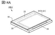
- FIG. 14 shows a semiconductor device 100I that is a modification of the semiconductor device 100H.
- 14A and 14B are perspective views of semiconductor device 100I.
- Semiconductor device 100I differs from semiconductor device 100H in that layer 20 is not provided.
- the layer 30, the sealing substrate 40, and the like are shown separately in order to make the configuration of the semiconductor device 100I easier to understand.
- the semiconductor device 100 ⁇ /b>I also includes a display driver circuit 23 and a pixel circuit 51 on the layer 30 .
- layer 30 may be formed with the necessary functional circuitry.
- power consumption and manufacturing cost of the semiconductor device can be reduced by not providing unnecessary functional circuits depending on the purpose and/or application.
- the thickness of the semiconductor device can be reduced, the weight can be reduced.
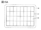
- FIG. 15A shows a configuration example when the display section 31 is divided into 32 sub-screens 35 .
- FIG. 15A shows the sub-screen 35 arranged in a matrix of 4 rows and 8 columns.
- the display frame frequency can be arbitrarily set (variable). Also, the display unit 31 can be driven for each sub-screen 35 . Therefore, the frame frequency can also be set for each sub-screen 35 .
- FIG. 15B shows an example in which a first drive circuit 232 and a second drive circuit 233 are provided in a region overlapping the sub-screen 35.
- FIG. 15B shows the position corresponding to the outer edge of the sub-screen 35 is indicated by a dashed line.
- FIG. 15B shows an example in which the first drive circuit 232 and the second drive circuit 233 provided for each sub-screen 35 are arranged so as to intersect at or near the center of each. The aspect is not limited to this.
- the memory cells 12 are not arranged in the region of the layer 10 overlapping the first driver circuit 232 and the second driver circuit 233. FIG. By doing so, the first drive circuit 232 and the second drive circuit 233 can be electrically connected to the sub-screen 35 in a short distance through the layer 10 .
- FIG. 16A shows a configuration example of layer 10 .
- the position corresponding to the outer edge of the sub-screen 35 is indicated by a dashed line.
- FIG. 16A shows an example in which a plurality of memory cells 12 are divided into four memory cell groups 15 in a region overlapping the sub-screen 35 .
- the space between the adjacent memory cell groups 15 is a region overlapping with the first driver circuit 232 and the second driver circuit 233 provided in the layer 20, and the memory cells 12 are not provided.
- FIG. 16B is a perspective view illustrating regions of layers 10, 20, and 30 overlapping one sub-screen 35.
- the first driver circuit 232 and the second driver circuit 233 are electrically connected to the sub-screen 35 by not providing the memory cell 12 in the region overlapping with the first driver circuit 232 and the second driver circuit 233 included in the layer 20.
- Conductor 55 can extend in the stacking direction of layers 10 , 20 , and 30 . Therefore, since the first drive circuit 232 and the second drive circuit 233 can be connected to the sub-screen 35 at an extremely short distance, wiring resistance and parasitic capacitance are small, and high-speed operation is possible. In addition, since deterioration of video signals is small, display quality of the semiconductor device is improved. Moreover, the power consumption of the semiconductor device can be reduced.
- the conductor 55 is composed of conductors and TSVs provided in each layer.
- the semiconductor device according to one aspect of the present invention can perform parallel processing of data communication between the GPU 22 and the storage unit 11 using a large number of wirings, for example. Therefore, the semiconductor device according to one embodiment of the present invention can operate at high speed.
- the semiconductor device according to one aspect of the present invention can process image data that has been arithmetically processed by the GPU 22 and stored in the storage unit 11 according to a communication standard such as HDMI (registered trademark), MIPI (registered trademark), or Display port. No need to compress. Therefore, the semiconductor device according to one embodiment of the present invention can operate at high speed and consume less power.
- a semiconductor device may include a display correction system.
- the display correction system can reduce display defects caused by defective pixels such as bright spots or dark spots.
- the circuit diagram shown in FIG. 17A shows a part of the pixel circuit 51 shown in FIG. 5A.
- the current IEL flowing through the light emitting element 61 is extremely large in the case of a defective pixel that causes a bright spot, compared to a normal display pixel. Also, the current IEL is extremely low in the case of a defective pixel causing a dark spot compared to a pixel with a normal display.
- the CPU 21 periodically acquires data on the monitor current IMONI flowing through the transistor 52C.
- the current amount of the monitor current IMONI is converted into digital data that can be handled by the CPU 21, and arithmetic processing is performed by the CPU 21 or GPU 22 using the digital data.
- a defective pixel is estimated by arithmetic processing in the CPU 21 or the GPU 22, and correction is performed to make it difficult to visually recognize a display defect caused by the defective pixel. For example, if the pixel 230D illustrated in FIG. 17B is a defective pixel, the current IEL flowing through the adjacent pixel 230N is corrected.
- the correction may be performed by artificial neural networks such as, for example, deep neural networks (DNN), convolutional neural networks (CNN), recurrent neural networks (RNN), autoencoders, deep Boltzmann machines (DBM), deep belief networks (DBN). It can be estimated by performing network-based operations.
- DNN deep neural networks
- CNN convolutional neural networks
- RNN recurrent neural networks
- DBM deep Boltzmann machines
- DBN deep belief networks
- the defective pixel 230D and the pixel 230N are combined and displayed as a pixel 230C (see FIG. 17C).
- display defects caused by defective pixels such as bright spots or dark spots are made difficult to see, and normal display can be brought closer.
- the semiconductor device in the above arithmetic processing, data in the middle of the arithmetic processing can be held in the storage portion 11 . Since the semiconductor device according to one embodiment of the present invention includes the display unit 31, the functional circuit 90, and the storage unit 11 in close proximity to each other, high-speed processing is possible when performing computation processing of a huge amount of computation such as computation based on an artificial neural network. can be realized, it is particularly effective.
- FIG. 18 is a cross-sectional view showing a configuration example of the semiconductor device 100A, showing a part of the semiconductor device 100A.
- the semiconductor device 100A is composed of the layers 10, 20, 30, 60, and the sealing substrate 40.
- Layer 10 has a substrate 701 on which a transistor 431 is provided.
- the transistor 431 is a transistor included in the memory cell 12, for example.
- a single crystal semiconductor substrate such as a single crystal silicon substrate can be used.
- a semiconductor substrate other than a single crystal semiconductor substrate may be used as the substrate 701 .
- the transistor 431 has a conductor 443 functioning as a gate electrode, an insulator 445 functioning as a gate insulator, and part of the substrate 701 .
- Part of the substrate 701 includes a region (semiconductor region 447) including a channel formation region of the transistor 431, a source region (either the low-resistance region 449a or the low-resistance region 449b), and a drain region (the low-resistance region 449a or the low-resistance region). 449b).
- the transistor 431 may be a p-channel transistor or an n-channel transistor.
- the transistor 431 is a transistor containing silicon in a channel formation region (also referred to as a "Si transistor").
- a transistor 431 is electrically isolated from other transistors by an element isolation layer 403 .
- FIG. 18 shows the case where the element isolation layer 403 electrically isolates the transistor 431 from other transistors.
- the element isolation layer 403 can be formed using a LOCOS (LOCal Oxidation of Silicon) method, an STI (Shallow Trench Isolation) method, or the like.
- the transistor 431 has a semiconductor region 447 with a convex shape.
- a conductor 443 is provided to cover the side and top surfaces of the semiconductor region 447 with the insulator 445 interposed therebetween. Note that FIG. 18 does not show how the conductor 443 covers the side surface of the semiconductor region 447 .
- a material that adjusts the work function can be used for the conductor 443 .
- a transistor in which a semiconductor region has a convex shape such as the transistor 431 can be called a fin transistor because it uses a convex portion of a semiconductor substrate.
- an insulator functioning as a mask for forming the projection may be provided in contact with the upper portion of the projection.
- FIG. 18 shows a structure in which part of the substrate 701 is processed to form a convex portion, a semiconductor having a convex shape may be formed by processing an SOI substrate.
- transistor 431 illustrated in FIG. 18 is an example, and is not limited to that structure, and an appropriate structure may be employed depending on the circuit structure, the operation method of the circuit, or the like.
- transistor 431 may be a planar transistor.
- An insulator 405 , an insulator 407 , an insulator 409 , and an insulator 411 are provided over the substrate 701 in addition to the element isolation layer 403 and the transistor 431 .
- Conductors 451 are embedded in the insulators 405 , 407 , 409 , and 411 .
- the height of the top surface of the conductor 451 and the height of the top surface of the insulator 411 can be made approximately the same.
- An insulator 421 and an insulator 422 are provided over the conductor 451 and the insulator 411 .
- Conductors 453 are embedded in the insulators 421 and 422 .
- the height of the top surface of the conductor 453 and the height of the top surface of the insulator 422 can be made approximately the same.
- An insulator 423 is provided over the conductor 453 and over the insulator 422 .
- a conductor 455 is embedded in the insulator 423 .
- the height of the top surface of the conductor 455 and the height of the top surface of the insulator 423 can be made approximately the same.
- the layer 10 may have a multilayer wiring structure by laminating insulators, conductors, and the like.
- Layer 20 has a substrate 702 on which transistors 441 and 442 are provided.
- the transistor 441 is a transistor included in the display section driving circuit 23, for example.
- the transistor 442 is, for example, a transistor included in the memory driver circuit 24 .
- a single crystal semiconductor substrate such as a single crystal silicon substrate can be used as in the case of the substrate 701 .
- a semiconductor substrate other than a single crystal semiconductor substrate may be used as the substrate 702 .
- Layer 20 may be constructed similarly to layer 10 . Therefore, a detailed description of layer 20 is omitted.
- the transistor 442 included in layer 20 and the transistor 431 included in layer 10 are electrically connected through the conductor 456 .
- Conductor 456 functions as a TSV. Note that the layers 10 and 20 may be electrically connected via a bump or the like.
- Layer 20 comprises conductors 760 .
- a conductor 760 is a conductor included in the terminal portion 29 .
- FIG. 18 shows an example in which a conductor 760 is electrically connected to an FPC 716 (Flexible Printed Circuit) via an anisotropic conductor 780 .
- FPC 716 Flexible Printed Circuit
- anisotropic conductor 780 Various signals are supplied to the semiconductor device 100A through the FPC 716 .
- the conductor 760 is electrically connected to the conductor 347 included in the layer 20 through the conductor 353 , the conductor 355 , and the conductor 357 .
- FIG. 18 shows three conductors, the conductor 353, the conductor 355, and the conductor 357, as conductors that electrically connect the conductor 760 and the conductor 347; however, one embodiment of the present invention is not limited to this. .
- the number of conductors that electrically connect the conductor 760 and the conductor 347 may be one, two, or four or more. By providing a plurality of conductors that electrically connect the conductor 760 and the conductor 347, contact resistance can be reduced.
- Layer 30 is provided on layer 20 .
- Layer 30 comprises insulator 214 on which transistor 750 is provided.
- the transistor 750 is a transistor included in the pixel circuit 51, for example.
- An OS transistor can be preferably used as the transistor 750 .
- An OS transistor has a feature of extremely low off-state current. Therefore, since the retention time of image data or the like can be lengthened, the frequency of refresh operations can be reduced. Therefore, the power consumption of the semiconductor device 100A can be reduced.
- the conductors 301 are embedded in the insulators 254 , 280 , 274 , and 281 .
- Conductor 301 a is electrically connected to one of the source and drain of transistor 750
- conductor 301 b is electrically connected to the other of the source and drain of transistor 750 .
- the height of the top surfaces of the conductors 301a and 301b and the height of the top surface of the insulator 281 can be approximately the same.
- a conductor 311 , a conductor 313 , a conductor 331 , a capacitor 790 , a conductor 333 , and a conductor 335 are embedded in the insulator 361 .
- Conductors 311 and 313 are electrically connected to transistor 750 and function as wirings.
- Conductor 333 and conductor 335 are electrically connected to capacitor 790 .
- the height of the top surfaces of the conductors 331, 333, and 335 and the height of the top surface of the insulator 361 can be approximately the same.
- a conductor 341 , a conductor 343 , and a conductor 351 are embedded in the insulator 363 .
- the height of the top surface of the conductor 351 and the height of the top surface of the insulator 363 can be made approximately the same.
- the body 363 has a function as an interlayer film, and may also have a function as a planarization film covering the uneven shape below each.
- the top surface of the insulator 363 may be planarized by planarization treatment using a chemical mechanical polishing (CMP) method or the like in order to improve planarity.
- CMP chemical mechanical polishing
- capacitor 790 has lower electrode 321 and upper electrode 325 .
- An insulator 323 is provided between the lower electrode 321 and the upper electrode 325 . That is, the capacitor 790 has a laminated structure in which the insulator 323 functioning as a dielectric is sandwiched between a pair of electrodes. Note that although FIG. 18 shows an example in which the capacitor 790 is provided over the insulator 281, the capacitor 790 may be provided over an insulator different from the insulator 281.
- FIG. 18 shows an example in which conductors 301a and 301b are formed in the same layer. Also, an example in which the conductor 311, the conductor 313, and the lower electrode 321 are formed in the same layer is shown. Further, an example in which the conductor 331, the conductor 333, and the conductor 335 are formed in the same layer is shown. Further, an example in which the conductor 341 and the conductor 343 are formed in the same layer is shown. Furthermore, an example in which the conductor 353, the conductor 355, and the conductor 357 are formed in the same layer is shown.
- the manufacturing process of the semiconductor device 100A can be simplified, so that the manufacturing cost of the semiconductor device 100A can be reduced. Note that they may be formed in different layers and may have different types of materials.
- Layer 60 is provided over layer 30 .
- Layer 60 comprises light emitting elements 61 .
- the light-emitting element 61 has a conductor 772 , an EL layer 786 and a conductor 788 .
- the EL layer 786 has an organic compound or an inorganic compound such as quantum dots.
- Materials that can be used for the organic compound include fluorescent materials, phosphorescent materials, and the like.
- Materials that can be used for quantum dots include colloidal quantum dot materials, alloy quantum dot materials, core-shell quantum dot materials, core quantum dot materials, and the like.
- Conductor 772 is electrically connected to the other of the source and drain of transistor 750 through conductor 351, conductor 341, conductor 331, conductor 313, and conductor 301b.
- a conductor 772 is formed over the insulator 363 and functions as a pixel electrode.
- a material that transmits or reflects visible light can be used for the conductor 772 .
- translucent materials include oxide materials containing indium and zinc, oxide materials containing indium, gallium and zinc (also referred to as "IGZO"), oxide materials containing indium and tin (“ITO ”, or an oxide material containing indium, tin, or silicon (also referred to as “ITSO”), or the like may be used.
- IGZO oxide materials containing indium and zinc
- ITO oxide materials containing indium and tin
- ITSO oxide material containing indium, tin, or silicon
- a reflective material for example, a material containing aluminum, silver, or the like may be used.
- the conductor 772 when the light emitted by the light emitting element 61 is emitted from the conductor 788 side, the conductor 772 preferably contains a reflective material.
- the conductor 772 may have a single-layer structure or a multi-layer structure.
- a three-layer structure in which silver is sandwiched between two layers of ITO may be employed.
- the conductor 772 may have a three-layer structure in which aluminum, titanium oxide, and ITO (or ITSO) are stacked in this order from the formation surface side. good. Further, in the case where the formation surface in contact with the conductor 772 contains silicon nitride, the conductor 772 may have a two-layer structure in which aluminum and IGZO are stacked in this order from the formation surface side.
- the conductor 301, the conductor 331, the conductor 351, the conductor 353, the conductor 355, the conductor 357, the conductor 453, the conductor 456, the conductor 760, and the like are the conductors described in other embodiments. It may be configured similarly to body 245 .
- the conductor 351 electrically connected to the light emitting element 61 may be a conductor containing tungsten and titanium nitride. More specifically, the sidewall of the insulator 363 and tungsten may be adjacent to each other with titanium nitride interposed therebetween.
- the semiconductor device 100A can be provided with optical members (optical substrates) such as a polarizing member, a retardation member, and an antireflection member.
- optical members optical substrates
- a polarizing member such as a polarizing member, a retardation member, and an antireflection member.
- the semiconductor device 100A shown in FIG. 18 has a top emission structure in which a reflective material is used for the conductor 772 and a translucent material is used for the conductor 788 so that the light emitting element 61 emits light toward the conductor 788. It can be a light-emitting element. Note that the light emitting element 61 may have a bottom emission structure in which light is emitted to the conductor 772 side, or a dual emission structure in which light is emitted to both the conductor 772 and the conductor 788 . Additionally, a structure 778 is provided.
- the sealing substrate 40 is provided above the layer 30 while covering the display section 31 and the layer 60 .
- the sealing substrate 40 is attached to the layer 30 with a sealing material 712 (also referred to as a "sealing material"). If the light emitting element 61 is a light emitting element with a top emission structure or a dual emission structure, a translucent material is used for the sealing substrate 40 .
- sealing substrate 40 By providing the sealing substrate 40, it is possible to prevent impurities from entering the layer 60 and improve the reliability of the semiconductor device 100A.
- a light shielding layer 738 is provided on the layer 60 side.
- the light blocking layer 738 has a function of blocking light emitted from adjacent regions.
- the light shielding layer 738 has a function of preventing external light from reaching the transistor 750 and the like.
- the light shielding layer 738 is covered with an insulator 734 .
- the insulator 734 may be provided as needed.
- a solid sealing structure in which the filling layer 732 is provided between the light emitting element 61 and the insulator 734 is shown; however, a hollow sealing structure in which the filling layer 732 is not provided may be employed.
- a portion corresponding to the filling layer 732 may be filled with an inert gas containing a Group 18 element (rare gas (noble gas)) and/or nitrogen. good.
- a Group 18 element ultraviolet gas (noble gas)
- a transistor including various semiconductors can be used as a transistor included in a semiconductor device according to one embodiment of the present invention.
- a transistor including a single crystal semiconductor, a polycrystalline semiconductor, a microcrystalline semiconductor, or an amorphous semiconductor for a channel formation region can be used.
- a compound semiconductor for example, SiGe, GaAs, etc.
- an oxide semiconductor or the like can be used instead of a single semiconductor whose main component is a single element.
- transistors with various structures can be used as the transistor included in the semiconductor device of one embodiment of the present invention.
- planar type FIN type (fin type), TRI-GATE type (tri-gate type), top gate type, bottom gate type, double gate type (gates are arranged above and below the channel), etc.
- a transistor having such a configuration can be used.
- a transistor according to one embodiment of the present invention a MOS transistor, a junction transistor, a bipolar transistor, or the like can be used.
- FIG. 19 A modification of the semiconductor device 100A shown in FIG. 18 is shown in FIG.
- the semiconductor device 100A shown in FIG. 19 differs from the semiconductor device 100A shown in FIG. 18 in that a colored layer 736 is provided.
- the colored layer 736 is provided so as to have a region overlapping with the light emitting element 61 .
- the color purity of the light extracted from the light emitting element 61 can be increased. Thereby, a high-quality image can be displayed on the semiconductor device 100A.
- all the light emitting elements 61 of the semiconductor device 100A can be light emitting elements that emit white light. can do.
- the light emitting element 61 can have a micro optical resonator (microcavity) structure.
- a predetermined color for example, RGB
- the semiconductor device 100A can perform color display. Absorption of light by the colored layer can be suppressed by adopting a structure in which the colored layer is not provided.
- the semiconductor device 100A can display a high-brightness image, and the power consumption of the semiconductor device 100A can be reduced.
- the luminance of the semiconductor device 100A is, for example, 500 cd/m 2 or more and 20000 cd/m 2 or less, preferably 1000 cd/m 2 or more and 20000 cd/m 2 or less, more preferably 5000 cd/m 2 or more and 20000 cd/m 2 or less. can.
- FIG. 20 shows a cross-sectional configuration example of a semiconductor device 100C, which is a modification of the semiconductor device 100A.
- a conductor 348 is provided on the insulator 361 of the layer 30 instead of the conductor 347 .
- Conductor 348 is electrically connected to conductor 760 through conductor 353 , conductor 355 , and conductor 357 . Conductor 348 functions similarly to conductor 347 .
- FIG. 21 shows an example of a cross-sectional structure in the case of a structure in which the layer 30 is overlaid on the layer 10 with the layer 20 interposed therebetween.
- FIG. 21 is a modification of the semiconductor device 100C.
- the layer 20 is provided over the layer 10 so that the transistors included in the layer 20 and the transistors included in the layer 10 face each other. Therefore, layer 30 is provided on the substrate 702 side of layer 20 .
- the conductor provided in the layer 10 and the conductor provided in the layer 20 can be electrically connected by, for example, a Cu--Cu bond.
- the conductor 455 provided in the layer 10 and the conductor 465 provided in the layer 20 are electrically connected by Cu--Cu bonding.
- the conductor 455 and the conductor 465 are formed using a conductor containing Cu (copper).
- the insulator 423 in which the conductor 455 is embedded and the insulator 424 in which the conductor 465 is embedded are preferably insulators containing the same element.
- each of the insulators 423 and 424 may be silicon oxide or silicon oxynitride.
- the bonding strength between the layers 10 and 20 is increased. Moreover, before bonding the layers 10 and 20 together, it is preferable to improve the flatness of both surfaces by, for example, performing a CMP process on the surfaces to be bonded together.
- bonding positions of the conductors 455 and 465 may or may not completely match depending on the alignment accuracy when bonding.
- FIG. 21 illustrates a case where they do not match completely.
- the conductor included in the layer 20 and the conductor included in the layer 30 may be electrically connected through a TSV.
- conductors 461 and 462 provided by layer 20 are both TSVs that penetrate substrate 702 .
- FIG. 22 shows a modification of the semiconductor device 100C.
- the cross-sectional configuration example shown in FIG. 22 shows an example in which the transistors included in the layer 30 are Si transistors.
- layer 30 comprises a substrate 703 on which a transistor 750 is provided.
- Substrate 703 is, for example, a monocrystalline silicon substrate. Therefore, the transistor 750 illustrated in FIG. 22 includes single crystal silicon in a semiconductor layer in which a channel is formed. Note that a substrate similar to the substrates 701 and 702 can be used as the substrate 703 .
- the layer 30 includes an insulator 361, an insulator 363, a conductor 348, a capacitor 790, etc. in addition to the structure similar to that of the layer 20.
- FIG. 1 shows insulator 361, an insulator 363, a conductor 348, a capacitor 790, etc. in addition to the structure similar to that of the layer 20.
- transistors other than OS transistors may be used as the transistors included in the layer 30 .
- Various transistors can be used as the transistors included in the layers 10, 20, and 30 depending on the purpose or application.
- a bump 454 and an adhesive layer 457 may be provided between layers 10 and 20 .
- Layers 10 and 20 are secured by adhesive layer 457 and electrically connected by bumps 454 .
- conductor 456 and conductor 455 are electrically connected via bump 454 .
- bumps 458 and adhesion layers 459 may be provided between layers 20 and 30 .
- Layers 20 and 30 are secured by adhesive layer 459 and electrically connected by bumps 458 .
- the number of bumps 454 electrically connecting the layers 10 and 20 is not limited to one, and may be plural.
- the number of bumps 458 electrically connecting the layers 20 and 30 is not limited to one, and may be plural.
- FIG. 24 shows a cross-sectional configuration example of a semiconductor device 100H, which is a modification of the semiconductor device 100C.
- FIG. 24 corresponds to the cross-sectional configuration of the semiconductor device 100C shown in FIG. 20 with the layer 10 removed. Since the semiconductor device 100H does not have the layer 10, it is not necessary to provide an element for electrically connecting the layers 10 and 20, such as the conductor 456.
- FIG. 24 shows a cross-sectional configuration example of a semiconductor device 100H, which is a modification of the semiconductor device 100C.
- FIG. 24 corresponds to the cross-sectional configuration of the semiconductor device 100C shown in FIG. 20 with the layer 10 removed. Since the semiconductor device 100H does not have the layer 10, it is not necessary to provide an element for electrically connecting the layers 10 and 20, such as the conductor 456.
- FIG. 25 shows a modification of the semiconductor device 100H.
- the cross-sectional configuration example shown in FIG. 25 shows an example in which the transistors included in the layer 30 are Si transistors.
- Layer 30 in FIG. 25 can be configured similarly to layer 30 shown in FIG.
- a bump 458 and an adhesive layer 459 may be provided between the layers 20 and 30 as shown in FIG. Layers 20 and 30 are secured by adhesive layer 459 and electrically connected by bumps 458 . As in the configuration example shown in FIG. 23, the number of bumps 458 electrically connecting the layers 20 and 30 is not limited to one, and may be plural.
- the layer 30 may be stacked on the layer 20 so that the transistor included in the layer 30 faces the transistor included in the layer 20 (see FIG. 27). ).
- insulator 361 and insulator 363 are provided over substrate 703 .
- a conductor 348 is provided over the insulator 361 .
- a conductor 341 and a conductor 351 are embedded in the insulator 363 .
- the conductor provided in the layer 20 and the conductor provided in the layer 30 can be electrically connected by, for example, a Cu--Cu bond.
- the conductor 465 provided in the layer 20 and the conductor 475 provided in the layer 30 are electrically connected by Cu--Cu bonding.
- the conductor 465 and the conductor 475 are formed using a conductor containing Cu (copper).
- the insulator 424 in which the conductor 465 is embedded and the insulator 425 in which the conductor 475 is embedded are preferably insulators containing the same element.
- each of the insulators 424 and 425 may be silicon oxide or silicon oxynitride.
- the bonding strength between the layers 20 and 30 is increased. Moreover, before bonding the layers 20 and 30 together, it is preferable to improve the flatness of both surfaces by performing a CMP process or the like on the surfaces to be bonded together.
- bonding positions of the conductors 465 and 475 may or may not completely match depending on the alignment accuracy when bonding.
- FIG. 27 illustrates a case where they do not match completely.
- the layer 30 may be provided with TSVs. Both conductors 471 and 472 shown in FIG. 27 are TSVs penetrating the substrate 703 . In FIG. 27, conductor 471 is electrically connected to conductor 341 . Conductor 472 is also electrically connected to conductor 348 .
- FIG. 28 shows a cross-sectional configuration example of the semiconductor device 100I.
- a semiconductor device 100I shown in FIG. 28 is a modification of the semiconductor device 100H shown in FIG. Therefore, FIG. 28 is a cross-sectional configuration example in the case where the transistors included in the layer 30 are composed of Si transistors.
- the semiconductor device 100 ⁇ /b>I includes the display driver circuit 23 and the pixel circuit 51 on the layer 30 .
- a transistor 750 in FIG. 28 is a transistor included in the pixel circuit 51, for example.
- a transistor 751 in FIG. 28 is, for example, a transistor included in the display driver circuit 23 .
- layer 30 may be formed with the necessary functional circuitry.
- power consumption and manufacturing cost of the semiconductor device can be reduced by not providing unnecessary functional circuits depending on the purpose and/or application.
- the thickness of the semiconductor device can be reduced, the weight can be reduced.
- the light emitting element 61 has an EL layer 786 between a pair of electrodes (conductors 772 and 788).
- EL layer 786 can be composed of multiple layers such as layer 4420 , light-emitting layer 4411 , and layer 4430 .
- the layer 4420 can have, for example, a layer containing a substance with high electron-injection properties (electron-injection layer) and a layer containing a substance with high electron-transport properties (electron-transporting layer).
- the light-emitting layer 4411 contains, for example, a light-emitting compound.
- Layer 4430 can have, for example, a layer containing a substance with high hole-injection properties (hole-injection layer) and a layer containing a substance with high hole-transport properties (hole-transport layer).
- a structure having layer 4420, light-emitting layer 4411, and layer 4430 provided between a pair of electrodes can function as a single light-emitting unit, and the structure in FIG. 29A is referred to as a single structure in this specification and the like.
- FIG. 29B is a modification of the EL layer 786 included in the light emitting element 61 shown in FIG. 29A.
- the light-emitting element 61 illustrated in FIG. 29B includes a layer 4430-1 over the conductor 772, a layer 4430-2 over the layer 4430-1, a light-emitting layer 4411 over the layer 4430-2, and a light-emitting layer It has layer 4420-1 on 4411, layer 4420-2 on layer 4420-1, and conductor 788 on layer 4420-2.
- layer 4430-1 functions as a hole injection layer
- layer 4430-2 functions as a hole transport layer
- layer 4420-1 functions as an electron Functioning as a transport layer
- layer 4420-2 functions as an electron injection layer.
- conductor 772 is the cathode and conductor 788 is the anode
- layer 4430-1 functions as an electron-injecting layer
- layer 4430-2 functions as an electron-transporting layer
- layer 4420-1 functions as a hole-transporting layer.
- a structure in which a plurality of light-emitting layers (light-emitting layers 4411, 4412, and 4413) are provided between layers 4420 and 4430 as shown in FIG. 29C is also an example of a single structure.
- tandem structure a structure in which a plurality of light-emitting units (EL layers 786a and 786b) are connected in series via an intermediate layer (charge-generating layer) 4440 is referred to herein as a tandem structure or It is called stack structure. Note that a tandem structure can realize a light-emitting element capable of emitting light with high luminance.
- the EL layers 786a and 786b may emit the same color.
- both the EL layer 786a and the EL layer 786b may emit green light.
- the display section 31 includes three sub-pixels of R, G, and B, and each sub-pixel has a light-emitting element, the light-emitting elements of each sub-pixel may have a tandem structure.
- the EL layers 786a and 786b of the R sub-pixel each have a material capable of emitting red light
- the EL layers 786a and 786b of the G sub-pixel each have a material capable of emitting green light.
- the EL layer 786a and the EL layer 786b of the B subpixel each contain a material capable of emitting blue light.
- the materials of the light-emitting layers 4411 and 4412 may be the same.
- the emission color of the light-emitting element can be red, green, blue, cyan, magenta, yellow, white, or the like, depending on the material forming the EL layer 786 . Further, the color purity can be further enhanced by providing the light-emitting element with a microcavity structure.
- the light-emitting layer may contain two or more light-emitting substances that emit light such as R (red), G (green), B (blue), Y (yellow), and O (orange).
- a light-emitting element that emits white light (also referred to as a “white light-emitting device”) preferably has a structure in which a light-emitting layer contains two or more kinds of light-emitting substances. In order to obtain white light emission, two or more light-emitting substances may be selected so that the light emission of each of the light-emitting substances has a complementary color relationship.
- the emission color of the first light-emitting layer and the emission color of the second light-emitting layer can be obtained.
- a light-emitting element having three or more light-emitting layers.
- the light-emitting layer preferably contains two or more light-emitting substances that emit light such as R (red), G (green), B (blue), Y (yellow), and O (orange).
- the luminescent material has two or more, and the emission of each luminescent material includes spectral components of two or more colors among R, G, and B.
- FIG. 30A shows a schematic top view of the light emitting element 61.
- the light emitting element 61 has a plurality of light emitting elements 61R exhibiting red, light emitting elements 61G exhibiting green, and light emitting elements 61B exhibiting blue.
- the light-emitting region of each light-emitting element is labeled with R, G, and B.
- the configuration of the light emitting element 61 shown in FIG. 30A may be called an SBS (side-by-side) structure.
- the configuration shown in FIG. 30A has three colors of red (R), green (G), and blue (B), the configuration is not limited to this. For example, it may be configured to have four or more colors.
- the light emitting elements 61R, 61G, and 61B are arranged in a matrix.
- FIG. 30A shows a so-called stripe arrangement in which light emitting elements of the same color are arranged in one direction. Note that the arrangement method of the light emitting elements is not limited to this, and an arrangement method such as a delta arrangement or a zigzag arrangement may be applied, or a pentile arrangement may be used.
- an organic EL device such as an OLED (Organic Light Emitting Diode) or a QLED (Quantum-dot Light Emitting Diode).
- OLED Organic Light Emitting Diode
- QLED Quantum-dot Light Emitting Diode
- Examples of light-emitting substances that EL devices have include substances that emit fluorescence (fluorescent materials), substances that emit phosphorescence (phosphorescent materials), inorganic compounds (quantum dot materials, etc.), and substances that exhibit heat-activated delayed fluorescence (heat-activated delayed fluorescence (thermally activated delayed fluorescence: TADF) material) and the like.
- FIG. 30B is a schematic cross-sectional view corresponding to the dashed-dotted line A1-A2 in FIG. 30A.
- FIG. 30B shows cross sections of the light emitting element 61R, the light emitting element 61G, and the light emitting element 61B.
- the light-emitting elements 61R, 61G, and 61B are provided over the insulating layer 251 and have a conductor 772 functioning as a pixel electrode and a conductor 788 functioning as a common electrode.
- the insulating layer 251 one or both of an inorganic insulating film and an organic insulating film can be used.
- An inorganic insulating film is preferably used as the insulating layer 251 .
- inorganic insulating films include oxide insulating films and nitride insulating films such as a silicon oxide film, a silicon oxynitride film, a silicon nitride oxide film, a silicon nitride film, an aluminum oxide film, an aluminum oxynitride film, and a hafnium oxide film. mentioned.
- the light emitting element 61R has an EL layer 786R between a conductor 772 functioning as a pixel electrode and a conductor 788 functioning as a common electrode.
- the EL layer 786R contains a light-emitting organic compound that emits light having an intensity in at least the red wavelength range.
- the EL layer 786G included in the light-emitting element 61G contains a light-emitting organic compound that emits light having an intensity in at least the green wavelength range.
- the EL layer 786B included in the light-emitting element 61B contains a light-emitting organic compound that emits light having an intensity in at least a blue wavelength range.
- Each of the EL layer 786R, the EL layer 786G, and the EL layer 786B includes an electron-injection layer, an electron-transport layer, a hole-injection layer, and a hole-transport layer in addition to a layer containing a light-emitting organic compound (light-emitting layer). You may have one or more of them.
- a conductor 772 functioning as a pixel electrode is provided for each light-emitting element.
- a conductor 788 functioning as a common electrode is provided as a continuous layer common to each light emitting element.
- One of the conductor 772 functioning as a pixel electrode and the conductor 788 functioning as a common electrode is a conductive film that transmits visible light, and the other is a reflective conductive film.
- the conductor 772 functioning as a pixel electrode is light-transmitting and the conductor 788 functioning as a common electrode is reflective, a bottom emission display device can be obtained.
- the conductor 772 functioning as a common electrode is reflective and the conductor 788 functioning as a common electrode is light-transmitting, a top emission display device can be obtained.
- both the conductor 772 functioning as a pixel electrode and the conductor 788 functioning as a common electrode are light-transmitting, whereby a dual-emission display device can be obtained.
- An insulating layer 272 is provided to cover an end portion of a conductor 772 functioning as a pixel electrode.
- the ends of the insulating layer 272 are preferably tapered.
- a material similar to the material that can be used for the insulating layer 251 can be used for the insulating layer 272 .
- Each of the EL layer 786R, the EL layer 786G, and the EL layer 786B has a region in contact with the top surface of the conductor 772 functioning as a pixel electrode and a region in contact with the surface of the insulating layer 272 .
- end portions of the EL layer 786R, the EL layer 786G, and the EL layer 786B are located over the insulating layer 272 .
- a gap is provided between the two EL layers between the light emitting elements of different colors.
- the EL layer 786R, the EL layer 786G, and the EL layer 786B are preferably provided so as not to be in contact with each other. This can suitably prevent current from flowing through two adjacent EL layers to cause unintended light emission (also referred to as crosstalk). Therefore, the contrast can be increased, and a display device with high display quality can be realized.
- the EL layer 786R, the EL layer 786G, and the EL layer 786B can be formed separately by a vacuum evaporation method or the like using a shadow mask such as a metal mask. Alternatively, these may be produced separately by photolithography. By using the photolithography method, it is possible to realize a high-definition display device that is difficult to achieve when using a metal mask.
- a device manufactured using a metal mask or FMM fine metal mask, high-definition metal mask
- a device with an MM (metal mask) structure is sometimes referred to as a device with an MML (metal maskless) structure.
- a protective layer 271 is provided over the conductor 788 functioning as a common electrode to cover the light emitting elements 61R, 61G, and 61B.
- the protective layer 271 has a function of preventing impurities such as water from diffusing into each light emitting element from above.
- the protective layer 271 can have, for example, a single-layer structure or a laminated structure including at least an inorganic insulating film.
- inorganic insulating films include oxide films and nitride films such as silicon oxide films, silicon oxynitride films, silicon nitride oxide films, silicon nitride films, aluminum oxide films, aluminum oxynitride films, and hafnium oxide films.
- a semiconductor material such as indium gallium oxide or indium gallium zinc oxide (IGZO) may be used as the protective layer 271 .
- the protective layer 271 may be formed using an ALD method, a CVD method, or a sputtering method.
- the structure including an inorganic insulating film as the protective layer 271 is exemplified, but the present invention is not limited to this.
- the protective layer 271 may have a laminated structure of an inorganic insulating film and an organic insulating film.
- a nitrided oxide refers to a compound containing more nitrogen than oxygen.
- An oxynitride is a compound containing more oxygen than nitrogen.
- the content of each element can be measured using, for example, Rutherford Backscattering Spectrometry (RBS).
- processing can be performed using a wet etching method or a dry etching method.
- a chemical solution such as oxalic acid, phosphoric acid, or a mixed chemical solution (for example, a mixed chemical solution of phosphoric acid, acetic acid, nitric acid, and water (also referred to as a mixed acid aluminum etchant)) is used.
- FIG. 30C shows an example different from the above. Specifically, FIG. 30C has a light emitting element 61W that emits white light.
- the light-emitting element 61W has an EL layer 786W that emits white light between a conductor 772 functioning as a pixel electrode and a conductor 788 functioning as a common electrode.
- the EL layer 786W can have, for example, a structure in which two or more light-emitting layers are stacked so that their emission colors are complementary.
- a laminated EL layer in which a charge generation layer is sandwiched between light emitting layers may be used.
- FIG. 30C shows three light emitting elements 61W side by side.
- a colored layer 264R is provided above the left light emitting element 61W.
- the colored layer 264R functions as a bandpass filter that transmits red light.
- a colored layer 264G that transmits green light is provided over the central light emitting element 61W
- a colored layer 264B that transmits blue light is provided over the right light emitting element 61W. This allows the display device to display a color image.
- an EL layer 786W and a conductor 788 functioning as a common electrode are separated from each other. This can prevent current from flowing through the EL layer 786W to cause unintended light emission in the two adjacent light emitting elements 61W.
- the EL layer 786W and the conductor 788 functioning as a common electrode are preferably separated by photolithography. As a result, the distance between the light emitting elements can be narrowed, so that a display device with a high aperture ratio can be realized as compared with the case of using a shadow mask such as a metal mask.
- a colored layer may be provided between the conductor 772 functioning as a pixel electrode and the insulating layer 251 .
- FIG. 30D shows an example different from the above. Specifically, FIG. 30D shows a configuration in which the insulating layer 272 is not provided between the light emitting elements 61R, 61G, and 61B. With such a structure, the display device can have a high aperture ratio. In addition, the protective layer 271 covers side surfaces of the EL layer 786R, the EL layer 786G, and the EL layer 786B. With such a structure, impurities (typically, water and the like) that can enter from side surfaces of the EL layers 786R, 786G, and 786B can be suppressed. In addition, in the structure shown in FIG.
- the conductor 772, the EL layer 786R, and the conductor 788 have approximately the same top surface shape.
- Such a structure can be formed at once using a resist mask or the like after the conductor 772, the EL layer 786R, and the conductor 788 are formed.
- Such a process can also be called self-aligned patterning because the EL layer 786R and the conductor 788 are processed using the conductor 788 as a mask.
- the EL layer 786R is described here, the EL layers 786G and 786B can have the same structure.
- FIG. 30D shows a structure in which a protective layer 273 is further provided on the protective layer 271.
- the protective layer 271 is formed using an apparatus capable of forming a film with high coverage (typically an ALD apparatus or the like), and the protective layer 273 is formed using a film with lower coverage than the protective layer 271.
- a region 275 can be provided between the protective layer 271 and the protective layer 273 by forming with an apparatus (typically, a sputtering apparatus or the like). In other words, the region 275 is located between the EL layer 786R and the EL layer 786G and between the EL layer 786G and the EL layer 786B.
- the region 275 has one or more selected from, for example, air, nitrogen, oxygen, carbon dioxide, and Group 18 elements (typically, helium, neon, argon, xenon, krypton, etc.). .
- the region 275 may contain a gas used for forming the protective layer 273, for example.
- the region 275 may contain any one or more of the Group 18 elements described above.
- the region 275 contains a gas
- the gas can be identified by a gas chromatography method or the like.
- the film of the protective layer 273 may contain the gas used for sputtering. In this case, an element such as argon may be detected when the protective layer 273 is analyzed by energy dispersive X-ray analysis (EDX analysis) or the like.
- EDX analysis energy dispersive X-ray analysis
- the refractive index of the region 275 is lower than that of the protective layer 271 , light emitted from the EL layer 786 R, EL layer 786 G, or EL layer 786 B is reflected at the interface between the protective layer 271 and the region 275 . Accordingly, light emitted from the EL layer 786R, the EL layer 786G, or the EL layer 786B can be prevented from entering adjacent pixels in some cases. As a result, it is possible to suppress the mixture of different emission colors from adjacent pixels, so that the display quality of the display device can be improved.
- the region between the light emitting elements 61R and 61G, or the region between the light emitting elements 61G and 61B can be narrowed.
- the distance between the light emitting elements is 1 ⁇ m or less, preferably 500 nm or less, more preferably 200 nm or less, 100 nm or less, 90 nm or less, 70 nm or less, 50 nm or less, 30 nm or less, 20 nm or less, 15 nm or less, or 10 nm.
- the distance between the side surface of the EL layer 786R and the side surface of the EL layer 786G or the distance between the side surface of the EL layer 786G and the side surface of the EL layer 786B is 1 ⁇ m or less, preferably 0.5 ⁇ m (500 nm). ), more preferably 100 nm or less.
- the region 275 contains gas, it is possible to suppress color mixture or crosstalk of light from each light emitting element while separating the light emitting elements.
- the region 275 may be filled with a filler.
- Fillers include epoxy resin, acrylic resin, silicone resin, phenol resin, polyimide resin, imide resin, PVC (polyvinyl chloride) resin, PVB (polyvinyl butyral) resin, EVA (ethylene vinyl acetate) resin, and the like.
- Photoresist may also be used as the filler.
- the photoresist used as the filler may be a positive photoresist or a negative photoresist.
- the white light emitting device when comparing the white light emitting device (single structure or tandem structure) and the light emitting device having the SBS structure, the light emitting device having the SBS structure can consume less power than the white light emitting device. If it is desired to keep power consumption low, it is preferable to use a light-emitting device with an SBS structure. On the other hand, the white light emitting device is preferable because the manufacturing process is simpler than that of the SBS structure light emitting device, so that the manufacturing cost can be lowered or the manufacturing yield can be increased.
- FIG. 31A shows an example different from the above. Specifically, the configuration shown in FIG. 31A differs from the configuration shown in FIG. 30D in the configuration of the insulating layer 251 .
- the insulating layer 251 has a concave portion due to a part of the upper surface thereof being shaved during processing of the light emitting elements 61R, 61G, and 61B.
- a protective layer 271 is formed in the recess. In other words, in a cross-sectional view, the lower surface of the protective layer 271 has a region located below the lower surface of the conductor 772 .
- impurities typically, water, etc.
- the above-described concave portion is used when removing impurities (also referred to as residue) that may adhere to the side surfaces of the light emitting elements 61R, 61G, and 61B by wet etching or the like during processing of the light emitting elements 61R, 61G, and 61B. can be formed.
- a protective layer 271 By covering the side surface of each light-emitting element with a protective layer 271 after removing the above residue, a highly reliable display device can be obtained.
- FIG. 31B shows an example different from the above.
- the configuration shown in FIG. 31B has an insulating layer 276 and a microlens array 277 in addition to the configuration shown in FIG. 31A.
- the insulating layer 276 functions as an adhesive layer.
- the microlens array 277 can collect light emitted from the light emitting elements 61R, 61G, and 61B. . Thereby, the light extraction efficiency of the display device can be improved.
- a bright image can be visually recognized, which is preferable.
- various curable adhesives such as photocurable adhesives such as ultraviolet curable adhesives, reaction curable adhesives, thermosetting adhesives, and anaerobic adhesives can be used.
- These adhesives include epoxy resins, acrylic resins, silicone resins, phenol resins, polyimide resins, imide resins, PVC (polyvinyl chloride) resins, PVB (polyvinyl butyral) resins, EVA (ethylene vinyl acetate) resins, and the like.
- a material with low moisture permeability such as epoxy resin is preferable.
- a two-liquid mixed type resin may be used.
- an adhesive sheet or the like may be used.
- FIG. 31C shows an example different from the above.
- the configuration shown in FIG. 31C has three light emitting elements 61W instead of the light emitting elements 61R, 61G, and 61B in the configuration shown in FIG. 31A.
- an insulating layer 276 is provided above the three light emitting elements 61W, and a colored layer 264R, a colored layer 264G, and a colored layer 264B are provided above the insulating layer 276.
- a colored layer 264R that transmits red light is provided at a position overlapping with the left light emitting element 61W
- a colored layer 264G that transmits green light is provided at a position overlapping with the central light emitting element 61W
- a colored layer 264G that transmits green light is provided at a position overlapping with the left light emitting element 61W.
- a colored layer 264B that transmits blue light is provided at a position overlapping with the light emitting element 61W. Accordingly, the semiconductor device can display a color image.
- the configuration shown in FIG. 31C is also a modification of the configuration shown in FIG. 30C.
- FIG. 31D shows an example different from the above. Specifically, in the configuration shown in FIG. 31D , the protective layer 271 is provided adjacent to the side surfaces of the conductor 772 and the EL layer 786 . In addition, the conductor 788 is provided as a continuous layer common to each light emitting element. Also, in the configuration shown in FIG. 31D, the region 275 is preferably filled with a filler material.
- the color purity of the emitted light can be enhanced.
- the product (optical distance) of the distance d between the conductor 772 and the conductor 788 and the refractive index n of the EL layer 786 is m times half the wavelength ⁇ . (m is an integer equal to or greater than 1).
- the distance d can be obtained by Equation (1).
- the distance d of the light emitting element 61 having a microcavity structure is determined according to the wavelength of the emitted light (emission color). Distance d corresponds to the thickness of EL layer 786 . Therefore, the EL layer 786G may be thicker than the EL layer 786B, and the EL layer 786R may be thicker than the EL layer 786G.
- the distance d is the distance from the reflective area of the conductor 772 functioning as a reflective electrode to the reflective area of the conductor 788 functioning as a semi-transmissive/semi-reflective electrode.
- the conductor 772 is a laminate of silver and ITO, which is a transparent conductive film, and the ITO is on the EL layer 786 side
- the distance d can be set according to the emission color by adjusting the film thickness of the ITO. That is, even if the EL layer 786R, the EL layer 786G, and the EL layer 786B have the same thickness, the distance d suitable for the emission color can be obtained by changing the thickness of the ITO.
- the light-emitting element 61 is composed of a hole-transport layer, a hole-transport layer, a light-emitting layer, an electron-transport layer, an electron-injection layer, and the like. A detailed configuration example of the light emitting element 61 will be described in another embodiment.
- the optical distance from the conductor 772 functioning as a reflective electrode to the light emitting layer is preferably an odd multiple of ⁇ /4. In order to realize the optical distance, it is preferable to appropriately adjust the thickness of each layer constituting the light emitting element 61 .
- the reflectance of the conductor 788 is preferably higher than the transmittance.
- the light transmittance of the conductor 788 is preferably 2% to 50%, more preferably 2% to 30%, further preferably 2% to 10%.
- ⁇ Structure example of transistor> 32A, 32B, and 32C are a top view and a cross-sectional view of a transistor 200 that can be used in a semiconductor device according to one embodiment of the present invention and the periphery of the transistor 200.
- FIG. The transistor 200 can be applied to the semiconductor device according to one embodiment of the present invention. For example, it can be used for the transistors that layer 30 comprises.
- FIG. 32A is a top view of transistor 200.
- FIG. 32B and 32C are cross-sectional views of the transistor 200.
- FIG. 32B is a cross-sectional view of the portion indicated by the dashed-dotted line A1-A2 in FIG. 32A, and is also a cross-sectional view of the transistor 200 in the channel length direction.
- 32C is a cross-sectional view of the portion indicated by the dashed-dotted line A3-A4 in FIG. 32A, and is also a cross-sectional view of the transistor 200 in the channel width direction.
- some elements are omitted for clarity of illustration.
- the transistor 200 includes a metal oxide 231a over a substrate (not shown), a metal oxide 231b over the metal oxide 231a, and a metal oxide 231b.
- conductors 242a and 242b spaced apart from each other, and an insulator 280 positioned over the conductors 242a and 242b and having an opening formed between the conductors 242a and 242b.
- the conductor 260 arranged in the opening, the metal oxide 231b, the conductor 242a, the conductor 242b, the insulator 280, the insulator 250 arranged between the conductor 260, the metal It has an oxide 231 b , a conductor 242 a , a conductor 242 b , an insulator 280 , and a metal oxide 231 c interposed between the insulator 250 .
- the top surface of conductor 260 preferably substantially coincides with the top surfaces of insulator 250, insulator 254, metal oxide 231c, and insulator 280.
- metal oxide 231a, the metal oxide 231b, and the metal oxide 231c may be collectively referred to as the metal oxide 231 below.
- the conductor 242a and the conductor 242b may be collectively referred to as a conductor 242 in some cases.
- the side surfaces of the conductors 242a and 242b on the conductor 260 side are substantially vertical.
- the angle between the side surfaces and the bottom surfaces of the conductors 242a and 242b is 10° to 80°, preferably 30° to 60°.
- the opposing side surfaces of the conductor 242a and the conductor 242b may have a plurality of surfaces.
- an insulator 254 is provided between an insulator 224, a metal oxide 231a, a metal oxide 231b, a conductor 242a, a conductor 242b, and a metal oxide 231c, and an insulator 280. preferably.
- the insulator 254 includes the side surface of the metal oxide 231c, the top and side surfaces of the conductor 242a, the top and side surfaces of the conductor 242b, the metal oxide 231a and the metal oxide 231b. , and the top surface of insulator 224 .
- the transistor 200 three layers of the metal oxide 231a, the metal oxide 231b, and the metal oxide 231c are stacked in a region where a channel is formed (hereinafter also referred to as a channel formation region) and its vicinity. , but the invention is not limited to this.
- a two-layer structure of the metal oxide 231b and the metal oxide 231c or a stacked structure of four or more layers may be provided.
- the conductor 260 has a two-layer structure in the transistor 200, the present invention is not limited to this.
- the conductor 260 may have a single-layer structure or a laminated structure of three or more layers.
- each of the metal oxide 231a, the metal oxide 231b, and the metal oxide 231c may have a laminated structure of two or more layers.
- the metal oxide 231c has a layered structure of a first metal oxide and a second metal oxide on the first metal oxide
- the first metal oxide is the metal oxide 231b.
- the second metal oxide preferably has a similar composition to metal oxide 231a.
- the conductor 260 functions as a gate electrode of the transistor, and the conductors 242a and 242b function as source and drain electrodes, respectively.
- the conductor 260 is formed to be embedded in the opening of the insulator 280 and the region between the conductors 242a and 242b.
- the arrangement of conductor 260, conductor 242a and conductor 242b is selected in a self-aligned manner with respect to the opening of insulator 280.
- the display device can have high definition.
- the display device can have a narrow frame.
- the conductor 260 preferably has a conductor 260a provided inside the insulator 250 and a conductor 260b provided so as to be embedded inside the conductor 260a.
- the transistor 200 includes an insulator 214 provided over a substrate (not shown), an insulator 216 provided over the insulator 214, and a conductor 205 embedded in the insulator 216. , insulator 222 disposed over insulator 216 and conductor 205 , and insulator 224 disposed over insulator 222 .
- a metal oxide 231 a is preferably disposed over the insulator 224 .
- An insulator 274 functioning as an interlayer film and an insulator 281 are preferably provided over the transistor 200 .
- the insulator 274 is preferably arranged in contact with top surfaces of the conductor 260 , the insulator 250 , the insulator 254 , the metal oxide 231 c , and the insulator 280 .
- the insulators 222, 254, and 274 preferably have a function of suppressing at least one diffusion of hydrogen (eg, hydrogen atoms, hydrogen molecules, or the like).
- insulators 222 , 254 , and 274 preferably have lower hydrogen permeability than insulators 224 , 250 , and 280 .
- the insulator 222 and the insulator 254 preferably have a function of suppressing diffusion of oxygen (eg, at least one of oxygen atoms, oxygen molecules, and the like).
- insulator 222 and insulator 254 preferably have lower oxygen permeability than insulator 224 , insulator 250 and insulator 280 .
- insulator 224 , metal oxide 231 , and insulator 250 are separated by insulators 280 and 281 and insulators 254 and 274 . Therefore, impurities such as hydrogen contained in the insulators 280 and 281 and excess oxygen can be prevented from entering the insulator 224 , the metal oxide 231 , and the insulator 250 .
- a conductor 245 (a conductor 245a and a conductor 245b) electrically connected to the transistor 200 and functioning as a plug is preferably provided.
- insulators 241 (insulators 241a and 241b) are provided in contact with side surfaces of conductors 245 functioning as plugs. That is, the insulator 241 is provided in contact with the inner walls of the openings of the insulator 254 , the insulator 280 , the insulator 274 , and the insulator 281 .
- a first conductor of the conductor 245 may be provided in contact with the side surface of the insulator 241 and a second conductor of the conductor 245 may be provided inside.
- the height of the upper surface of the conductor 245 and the height of the upper surface of the insulator 281 can be made approximately the same.
- the transistor 200 shows the structure in which the first conductor of the conductor 245 and the second conductor of the conductor 245 are stacked, the present invention is not limited to this.
- the conductor 245 may be provided as a single layer or a laminated structure of three or more layers. When the structure has a laminated structure, an ordinal number may be assigned in order of formation for distinction.
- metal oxides functioning as oxide semiconductors are added to metal oxides 231 (metal oxides 231a, 231b, and 231c) including a channel formation region. ) is preferably used.
- the metal oxide preferably contains at least indium (In) or zinc (Zn). In particular, it preferably contains indium (In) and zinc (Zn). Moreover, in addition to these, it is preferable that the element M is included.
- element M aluminum (Al), gallium (Ga), yttrium (Y), tin (Sn), boron (B), titanium (Ti), iron (Fe), nickel (Ni), germanium (Ge), zirconium (Zr), molybdenum (Mo), lanthanum (La), cerium (Ce), neodymium (Nd), hafnium (Hf), tantalum (Ta), tungsten (W), magnesium (Mg) or cobalt (Co)
- element M aluminum (Al), gallium (Ga), yttrium (Y), tin (Sn), boron (B), titanium (Ti), iron (Fe), nickel (Ni), germanium (Ge), zirconium (Zr), molyb
- the element M is preferably one or more of aluminum (Al), gallium (Ga), yttrium (Y), and tin (Sn). Moreover, it is more preferable that the element M contains either one or both of gallium (Ga) and tin (Sn).
- the thickness of the metal oxide 231b in a region that does not overlap with the conductor 242 may be thinner than that in a region that overlaps with the conductor 242 .
- This is formed by removing a portion of the top surface of metal oxide 231b when forming conductors 242a and 242b.
- a region with low resistance is formed near the interface with the conductive film in some cases.
- a high-definition display device including a small-sized transistor can be provided.
- a display device including a transistor with high on-state current and high luminance can be provided.
- a fast-operating display device can be provided with a fast-operating transistor.
- a highly reliable display device including a transistor with stable electrical characteristics can be provided.
- a display device including a transistor with low off-state current and low power consumption can be provided.
- transistor 200 A detailed structure of the transistor 200 that can be used in the display device that is one embodiment of the present invention is described.
- the conductor 205 is arranged so as to have regions that overlap with the metal oxide 231 and the conductor 260 . Further, the conductor 205 is preferably embedded in the insulator 216 .
- the conductor 205 has a conductor 205a, a conductor 205b, and a conductor 205c.
- Conductor 205 a is provided in contact with the bottom surface and sidewalls of the opening provided in insulator 216 .
- the conductor 205b is provided so as to be embedded in a recess formed in the conductor 205a.
- the top surface of the conductor 205b is lower than the top surface of the conductor 205a and the top surface of the insulator 216 .
- the conductor 205c is provided in contact with the top surface of the conductor 205b and the side surface of the conductor 205a.
- the height of the upper surface of the conductor 205c substantially matches the height of the upper surface of the conductor 205a and the height of the upper surface of the insulator 216.
- the conductor 205a and the conductor 205c are conductive materials having a function of suppressing diffusion of impurities such as hydrogen atoms, hydrogen molecules, water molecules, nitrogen atoms, nitrogen molecules, nitrogen oxide molecules (NO, NO, NO2, etc.), and copper atoms. It is preferable to use a flexible material. Alternatively, it is preferable to use a conductive material having a function of suppressing diffusion of oxygen (eg, at least one of oxygen atoms, oxygen molecules, and the like).
- the conductor 205a By using a conductive material having a function of reducing diffusion of hydrogen for the conductor 205a and the conductor 205c, impurities such as hydrogen contained in the conductor 205b pass through the insulator 224 or the like to the metal oxide 231. can be suppressed.
- a conductive material having a function of suppressing diffusion of oxygen for the conductors 205a and 205c it is possible to suppress reduction in conductivity due to oxidation of the conductor 205b.
- the conductive material having a function of suppressing diffusion of oxygen titanium, titanium nitride, tantalum, tantalum nitride, ruthenium, ruthenium oxide, or the like is preferably used, for example. Therefore, the conductor 205a may be a single layer or a laminate of the above conductive materials.
- the conductor 205a may be titanium nitride.
- a conductive material containing tungsten, copper, or aluminum as its main component is preferably used for the conductor 205b.
- tungsten may be used for the conductor 205b.
- the conductor 260 may function as a first gate (also referred to as a top gate) electrode.
- the conductor 205 functions as a second gate (also referred to as a bottom gate) electrode.
- V th of the transistor 200 can be controlled by changing the potential applied to the conductor 205 independently of the potential applied to the conductor 260 .
- V th of the transistor 200 can be made higher than 0 V and the off-state current can be reduced. Therefore, when a negative potential is applied to the conductor 205, the drain current when the potential applied to the conductor 260 is 0 V can be made smaller than when no potential is applied.
- the conductor 205 is preferably provided larger than the channel formation region in the metal oxide 231 .
- the conductor 205 preferably extends even in a region outside the edge crossing the channel width direction of the metal oxide 231 .
- the conductor 205 and the conductor 260 preferably overlap with each other with an insulator interposed therebetween on the outside of the side surface of the metal oxide 231 in the channel width direction.
- the electric field of the conductor 260 functioning as the first gate electrode and the electric field of the conductor 205 functioning as the second gate electrode cause the channel formation region of the metal oxide 231 to be expanded. It can be surrounded electrically.
- the conductor 205 is extended so that it also functions as a wire.
- a structure in which a conductor functioning as a wiring is provided under the conductor 205 may be employed.
- the insulator 214 preferably functions as a barrier insulating film that prevents impurities such as water or hydrogen from entering the transistor 200 from the substrate side. Therefore, the insulator 214 has a function of suppressing the diffusion of impurities such as hydrogen atoms, hydrogen molecules, water molecules, nitrogen atoms, nitrogen molecules, nitrogen oxide molecules (N 2 O, NO, NO 2 and the like), and copper atoms. (It is difficult for the above impurities to permeate.) It is preferable to use an insulating material. Alternatively, it is preferable to use an insulating material that has a function of suppressing the diffusion of oxygen (eg, at least one of oxygen atoms, oxygen molecules, and the like) (the oxygen hardly permeates).
- oxygen eg, at least one of oxygen atoms, oxygen molecules, and the like
- the insulator 214 is preferably made of aluminum oxide, silicon nitride, or the like. Accordingly, impurities such as water or hydrogen can be prevented from diffusing from the substrate side to the transistor 200 side with respect to the insulator 214 . Alternatively, diffusion of oxygen contained in the insulator 224 or the like to the substrate side of the insulator 214 can be suppressed.
- the insulators 216 , 280 , and 281 that function as interlayer films preferably have lower dielectric constants than the insulator 214 .
- the parasitic capacitance generated between wirings can be reduced.
- the insulator 216, the insulator 280, and the insulator 281 include silicon oxide, silicon oxynitride, silicon nitride oxide, silicon nitride, silicon oxide to which fluorine is added, silicon oxide to which carbon is added, and carbon and nitrogen are added. Silicon oxide, silicon oxide having holes, or the like may be used as appropriate.
- Insulator 222 and insulator 224 function as gate insulators.
- the insulator 224 in contact with the metal oxide 231 preferably releases oxygen by heating.
- the oxygen released by heating is sometimes referred to as excess oxygen.
- silicon oxide, silicon oxynitride, or the like may be used as appropriate for the insulator 224 .
- an oxide material from which part of oxygen is released by heating is preferably used as the insulator 224 .
- the oxide from which oxygen is released by heating means that the amount of oxygen released in terms of oxygen atoms is 1.0 ⁇ 10 18 atoms/cm 3 or more, preferably 1.0, in TDS (Thermal Desorption Spectroscopy) analysis. It is an oxide film having a density of 10 19 atoms/cm 3 or more, more preferably 2.0 10 19 atoms/cm 3 or more, or 3.0 10 20 atoms/cm 3 or more.
- the surface temperature of the film during the TDS analysis is preferably in the range of 100° C. or higher and 700° C. or lower, or 100° C. or higher and 400° C. or lower.
- the insulator 224 may have a thinner film thickness in a region that does not overlap with the insulator 254 and does not overlap with the metal oxide 231b than in other regions.
- the thickness of the region of the insulator 224 which does not overlap with the insulator 254 and does not overlap with the metal oxide 231b is preferably a thickness with which oxygen can be diffused sufficiently.
- the insulator 222 preferably functions as a barrier insulating film that prevents impurities such as water or hydrogen from entering the transistor 200 from the substrate side.
- insulator 222 preferably has a lower hydrogen permeability than insulator 224 .
- the insulator 222 preferably has a function of suppressing diffusion of oxygen (eg, at least one of oxygen atoms, oxygen molecules, and the like) (the above-mentioned oxygen is difficult to permeate).
- oxygen eg, at least one of oxygen atoms, oxygen molecules, and the like
- insulator 222 preferably has a lower oxygen permeability than insulator 224 .
- the insulator 222 preferably has a function of suppressing diffusion of oxygen and impurities, so that diffusion of oxygen in the metal oxide 231 to the substrate side can be reduced. Further, the conductor 205 can be prevented from reacting with oxygen contained in the insulator 224 and the metal oxide 231 .
- the insulator 222 preferably contains an oxide of one or both of aluminum and hafnium, which are insulating materials.
- the insulator containing oxide of one or both of aluminum and hafnium aluminum oxide, hafnium oxide, oxide containing aluminum and hafnium (hafnium aluminate), or the like is preferably used.
- oxygen is released from the metal oxide 231 and impurities such as hydrogen enter the metal oxide 231 from the periphery of the transistor 200 . It functions as a layer that suppresses
- aluminum oxide, bismuth oxide, germanium oxide, niobium oxide, silicon oxide, titanium oxide, tungsten oxide, yttrium oxide, or zirconium oxide may be added to these insulators.
- these insulators may be nitrided. Silicon oxide, silicon oxynitride, or silicon nitride may be stacked over the above insulator.
- the insulator 222 is made of, for example, a so-called high oxide such as aluminum oxide, hafnium oxide, tantalum oxide, zirconium oxide, lead zirconate titanate (PZT), strontium titanate (SrTiO 3 ) or (Ba,Sr)TiO 3 (BST). Insulators including -k materials may be used in single layers or stacks. As transistors are miniaturized and highly integrated, thinning of gate insulators may cause problems such as leakage current. By using a high-k material for an insulator that functions as a gate insulator, it is possible to reduce the gate potential during transistor operation while maintaining the physical film thickness.
- a so-called high oxide such as aluminum oxide, hafnium oxide, tantalum oxide, zirconium oxide, lead zirconate titanate (PZT), strontium titanate (SrTiO 3 ) or (Ba,Sr)TiO 3 (BST).
- Insulators including -k materials may be
- the insulator 222 and the insulator 224 may have a stacked structure of two or more layers. In that case, it is not limited to a laminated structure made of the same material, and a laminated structure made of different materials may be used. For example, an insulator similar to the insulator 224 may be provided under the insulator 222 .
- the metal oxide 231 has a metal oxide 231a, a metal oxide 231b over the metal oxide 231a, and a metal oxide 231c over the metal oxide 231b.
- a metal oxide 231a under the metal oxide 231b, it is possible to suppress the diffusion of impurities from the structure formed below the metal oxide 231a to the metal oxide 231b.
- the metal oxide 231c over the metal oxide 231b, diffusion of impurities from the structure formed above the metal oxide 231c to the metal oxide 231b can be suppressed.
- the metal oxide 231 preferably has a laminated structure of a plurality of oxide layers with different atomic ratios of metal atoms.
- the metal oxide 231 contains at least indium (In) and the element M
- the number of atoms of the element M contained in the metal oxide 231a with respect to the number of atoms of all elements constituting the metal oxide 231a The ratio is preferably higher than the ratio of the number of atoms of the element M contained in the metal oxide 231b to the number of atoms of all elements forming the metal oxide 231b.
- the atomic ratio of the element M contained in the metal oxide 231a to In is preferably higher than the atomic ratio of the element M contained in the metal oxide 231b to In.
- the metal oxide 231c can be a metal oxide that can be used for the metal oxide 231a or the metal oxide 231b.
- the energy of the conduction band bottom of the metal oxide 231a and the metal oxide 231c be higher than the energy of the conduction band bottom of the metal oxide 231b.
- the electron affinities of the metal oxides 231a and 231c are preferably smaller than the electron affinities of the metal oxide 231b.
- the metal oxide 231c is preferably a metal oxide that can be used for the metal oxide 231a.
- the ratio of the number of atoms of the element M contained in the metal oxide 231c to the number of atoms of all the elements forming the metal oxide 231c is higher than the number of atoms of all the elements forming the metal oxide 231b.
- the atomic ratio of the element M contained in the metal oxide 231c to In is preferably higher than the atomic ratio of the element M contained in the metal oxide 231b to In.
- the energy level at the bottom of the conduction band changes smoothly at the junction of the metal oxide 231a, the metal oxide 231b, and the metal oxide 231c.
- the energy level of the bottom of the conduction band at the junction of the metal oxide 231a, the metal oxide 231b, and the metal oxide 231c continuously changes or continuously joins.
- the metal oxide 231a and the metal oxide 231b, and the metal oxide 231b and the metal oxide 231c have a common element (main component) other than oxygen, so that the defect level density is low.
- Mixed layers can be formed.
- the metal oxide 231b is an In-Ga-Zn oxide
- the metal oxide 231a and the metal oxide 231c may be In-Ga-Zn oxide, Ga-Zn oxide, gallium oxide, or the like.
- the metal oxide 231c may have a laminated structure.
- a stacked structure of In--Ga--Zn oxide and Ga--Zn oxide over the In--Ga--Zn oxide, or an In--Ga--Zn oxide and over the In--Ga--Zn oxide can be used.
- a stacked structure of an In--Ga--Zn oxide and an oxide that does not contain In may be used as the metal oxide 231c.
- the metal oxide 231c has a stacked structure
- the main path of carriers becomes the metal oxide 231b.
- the defect level density at the interface between the metal oxide 231a and the metal oxide 231b and at the interface between the metal oxide 231b and the metal oxide 231c can be reduced. can be lowered. Therefore, the influence of interface scattering on carrier conduction is reduced, and the transistor 200 can obtain high on-current and high frequency characteristics.
- the constituent elements of the metal oxide 231c are It is expected to suppress the diffusion to the insulator 250 side.
- the metal oxide 231c has a stacked structure, and the oxide that does not contain In is positioned above the stacked structure, so that In that can diffuse toward the insulator 250 can be suppressed. Since the insulator 250 functions as a gate insulator, the characteristics of the transistor deteriorate when In is diffused. Therefore, by forming the metal oxide 231c into a stacked structure, a highly reliable display device can be provided.
- a conductor 242 (a conductor 242a and a conductor 242b) functioning as a source electrode and a drain electrode is provided over the metal oxide 231b.
- Conductors 242 include aluminum, chromium, copper, silver, gold, platinum, tantalum, nickel, titanium, molybdenum, tungsten, hafnium, vanadium, niobium, manganese, magnesium, zirconium, beryllium, indium, ruthenium, iridium, strontium, and lanthanum. It is preferable to use a metal element selected from, an alloy containing the above-described metal elements as a component, or an alloy in which the above-described metal elements are combined.
- tantalum nitride, titanium nitride, tungsten, nitride containing titanium and aluminum, nitride containing tantalum and aluminum, ruthenium oxide, ruthenium nitride, oxide containing strontium and ruthenium, oxide containing lanthanum and nickel, and the like are used. is preferred.
- tantalum nitride, titanium nitride, nitrides containing titanium and aluminum, nitrides containing tantalum and aluminum, ruthenium oxide, ruthenium nitride, oxides containing strontium and ruthenium, and oxides containing lanthanum and nickel are difficult to oxidize. It is preferable because it is a conductive material or a material that maintains conductivity even after absorbing oxygen.
- the oxygen concentration in the vicinity of the conductor 242 of the metal oxide 231 may be reduced.
- a metal compound layer containing the metal contained in the conductor 242 and the components of the metal oxide 231 is formed in the vicinity of the conductor 242 of the metal oxide 231 .
- the carrier concentration increases in the region of the metal oxide 231 near the conductor 242, and the region becomes a low-resistance region.
- a region between the conductor 242a and the conductor 242b is formed so as to overlap with the opening of the insulator 280.
- the conductor 260 can be arranged in a self-aligned manner between the conductor 242a and the conductor 242b.
- Insulator 250 functions as a gate insulator.
- the insulator 250 is preferably arranged in contact with the top surface of the metal oxide 231c.
- silicon oxide, silicon oxynitride, silicon nitride oxide, silicon nitride, silicon oxide to which fluorine is added, silicon oxide to which carbon is added, silicon oxide to which carbon and nitrogen are added, or silicon oxide having vacancies is used. be able to.
- silicon oxide and silicon oxynitride are preferable because they are stable against heat.
- the insulator 250 preferably has a reduced impurity concentration such as water or hydrogen.
- the thickness of the insulator 250 is preferably 1 nm or more and 20 nm or less.
- a metal oxide may be provided between the insulator 250 and the conductor 260 .
- the metal oxide preferably suppresses oxygen diffusion from the insulator 250 to the conductor 260 . Accordingly, oxidation of the conductor 260 by oxygen in the insulator 250 can be suppressed.
- the metal oxide may function as part of the gate insulator. Therefore, in the case where silicon oxide, silicon oxynitride, or the like is used for the insulator 250, a metal oxide that is a high-k material with a high dielectric constant is preferably used as the metal oxide.
- the gate insulator has a stacked-layer structure of the insulator 250 and the metal oxide, the stacked-layer structure can be stable against heat and have a high relative dielectric constant. Therefore, the gate potential applied during transistor operation can be reduced while maintaining the physical film thickness of the gate insulator. Also, the equivalent oxide thickness (EOT) of the insulator that functions as the gate insulator can be reduced.
- EOT equivalent oxide thickness
- a metal oxide containing one or more selected from hafnium, aluminum, gallium, yttrium, zirconium, tungsten, titanium, tantalum, nickel, germanium, magnesium, or the like can be used.
- the conductor 260 is shown as having a two-layer structure in FIG. 32, it may have a single-layer structure or a laminated structure of three or more layers.
- the conductor 260a has a function of suppressing the diffusion of impurities such as hydrogen atoms, hydrogen molecules, water molecules, nitrogen atoms, nitrogen molecules, nitrogen oxide molecules (N 2 O, NO, NO 2 and the like), and copper atoms. It is preferable to use a conductor having a Alternatively, it is preferable to use a conductive material having a function of suppressing diffusion of oxygen (eg, at least one of oxygen atoms, oxygen molecules, and the like).
- the conductor 260a has a function of suppressing diffusion of oxygen
- oxygen contained in the insulator 250 can suppress oxidation of the conductor 260b and a decrease in conductivity.
- the conductive material having a function of suppressing diffusion of oxygen tantalum, tantalum nitride, ruthenium, ruthenium oxide, or the like is preferably used, for example.
- a conductive material containing tungsten, copper, or aluminum as its main component is preferably used for the conductor 260b.
- the conductor 260 since the conductor 260 also functions as a wiring, a conductor with high conductivity is preferably used.
- a conductive material whose main component is tungsten, copper, or aluminum can be used.
- the conductor 260b may have a layered structure, for example, a layered structure of titanium or titanium nitride and the above conductive material.
- the side surfaces of the metal oxide 231 are covered with the conductor 260 in the region of the metal oxide 231b that does not overlap with the conductor 242, in other words, the channel formation region of the metal oxide 231. are placed.
- the insulator 254 preferably functions as a barrier insulating film that prevents impurities such as water or hydrogen from entering the transistor 200 from the insulator 280 side.
- insulator 254 preferably has a lower hydrogen permeability than insulator 224 .
- the insulator 254 includes the side surfaces of the metal oxide 231c, the top and side surfaces of the conductor 242a, the top and side surfaces of the conductor 242b, and the metal oxide 231a and the metal oxide 231b. It preferably touches the sides as well as the top surface of the insulator 224 .
- hydrogen contained in the insulator 280 enters the metal oxide 231 from the top surface or the side surface of the conductor 242a, the conductor 242b, the metal oxide 231a, the metal oxide 231b, and the insulator 224. can be suppressed.
- the insulator 254 preferably has a function of suppressing the diffusion of oxygen (eg, at least one of oxygen atoms, oxygen molecules, and the like) (the oxygen is less permeable).
- insulator 254 preferably has a lower oxygen permeability than insulator 280 or insulator 224 .
- the insulator 254 is preferably deposited using a sputtering method.
- oxygen can be added to the vicinity of a region of the insulator 224 which is in contact with the insulator 254 . Accordingly, oxygen can be supplied from the region through the insulator 224 into the metal oxide 231 .
- the insulator 254 has a function of suppressing upward diffusion of oxygen, diffusion of oxygen from the metal oxide 231 to the insulator 280 can be prevented.
- the insulator 222 has a function of suppressing diffusion of oxygen downward, oxygen can be prevented from diffusing from the metal oxide 231 to the substrate side. In this manner, oxygen is supplied to the channel formation region of the metal oxide 231 . Accordingly, oxygen vacancies in the metal oxide 231 can be reduced, and normally-on of the transistor can be suppressed.
- an insulator containing an oxide of one or both of aluminum and hafnium is preferably deposited.
- the insulator containing oxides of one or both of aluminum and hafnium aluminum oxide, hafnium oxide, an oxide containing aluminum and hafnium (hafnium aluminate), or the like is preferably used.
- the insulator 224 , the insulator 250 , and the metal oxide 231 are covered with the insulator 254 having a barrier property against hydrogen; and isolated from the insulator 250 .
- the insulator 254 having a barrier property against hydrogen; and isolated from the insulator 250 .
- the concentration of impurities such as water or hydrogen in the insulator 280 is reduced. Also, the upper surface of the insulator 280 may be flattened.
- the insulator 274 preferably functions as a barrier insulating film that prevents impurities such as water or hydrogen from entering the insulator 280 from above.
- the insulator 274 an insulator that can be used for the insulator 214, the insulator 254, or the like may be used, for example.
- An insulator 281 functioning as an interlayer film is preferably provided over the insulator 274 .
- the insulator 281 preferably has a reduced concentration of impurities such as water or hydrogen in the film.
- the conductors 245 a and 245 b are arranged in openings formed in the insulators 281 , 274 , 280 , and 254 .
- the conductor 245a and the conductor 245b are provided to face each other with the conductor 260 interposed therebetween. Note that the top surfaces of the conductors 245 a and 245 b may be flush with the top surface of the insulator 281 .
- the insulator 241a is provided in contact with the inner walls of the openings of the insulator 281, the insulator 274, the insulator 280, and the insulator 254, and the first conductor of the conductor 245a is formed in contact with the side surface thereof. ing.
- a conductor 242a is positioned at least part of the bottom of the opening, and the conductor 245a is in contact with the conductor 242a.
- the insulator 241b is provided in contact with the inner walls of the openings of the insulator 281, the insulator 274, the insulator 280, and the insulator 254, and the first conductor of the conductor 245b is formed in contact with the side surface thereof. It is The conductor 242b is positioned at least part of the bottom of the opening, and the conductor 245b is in contact with the conductor 242b.
- a conductive material containing tungsten, copper, or aluminum as its main component is preferably used for the conductors 245a and 245b.
- the conductor 245a and the conductor 245b may have a laminated structure.
- the conductor 245 has a layered structure
- a conductor having a function of suppressing diffusion of impurities such as hydrogen is preferably used.
- tantalum, tantalum nitride, titanium, titanium nitride, ruthenium, ruthenium oxide, or the like is preferably used.
- the conductive material having a function of suppressing diffusion of impurities such as water or hydrogen may be used in a single layer or a stacked layer. By using the conductive material, absorption of oxygen added to the insulator 280 by the conductors 245a and 245b can be suppressed.
- impurities such as water or hydrogen from a layer above the insulator 281 can be prevented from entering the metal oxide 231 through the conductors 245a and 245b.
- An insulator that can be used for the insulator 254 or the like may be used as the insulator 241a and the insulator 241b, for example. Since the insulators 241a and 241b are provided in contact with the insulator 254, impurities such as water or hydrogen from the insulator 280 or the like are prevented from entering the metal oxide 231 through the conductors 245a and 245b. can. In addition, absorption of oxygen contained in the insulator 280 by the conductors 245a and 245b can be suppressed.
- a conductor functioning as a wiring may be arranged in contact with the top surface of the conductor 245a and the top surface of the conductor 245b.
- a conductive material containing tungsten, copper, or aluminum as a main component is preferably used for the conductor functioning as the wiring.
- the conductor may have a laminated structure, for example, a laminated structure of titanium or titanium nitride and the above conductive material. The conductor may be formed so as to be embedded in an opening provided in the insulator.
- an insulator substrate, a semiconductor substrate, or a conductor substrate may be used, for example.
- insulator substrates include glass substrates, quartz substrates, sapphire substrates, stabilized zirconia substrates (yttria stabilized zirconia substrates, etc.), resin substrates, and the like.
- semiconductor substrates include semiconductor substrates such as silicon and germanium, and compound semiconductor substrates made of silicon carbide, silicon germanium, gallium arsenide, indium phosphide, zinc oxide, and gallium oxide.
- semiconductor substrate having an insulator region inside the semiconductor substrate such as an SOI (Silicon On Insulator) substrate.
- Examples of conductive substrates include graphite substrates, metal substrates, alloy substrates, and conductive resin substrates. Alternatively, there are a substrate having a metal nitride, a substrate having a metal oxide, and the like. Furthermore, there are substrates in which an insulator substrate is provided with a conductor or a semiconductor, a substrate in which a semiconductor substrate is provided with a conductor or an insulator, a substrate in which a conductor substrate is provided with a semiconductor or an insulator, and the like. Alternatively, these substrates provided with elements may be used. Elements provided on the substrate include a capacitive element, a resistance element, a switch element, a light emitting element, a memory element, and the like.
- Insulator examples include oxides, nitrides, oxynitrides, nitride oxides, metal oxides, metal oxynitrides, metal nitride oxides, and the like, which have insulating properties.
- thinning of gate insulators may cause problems such as leakage current.
- a high-k material for an insulator functioning as a gate insulator voltage reduction during transistor operation can be achieved while maintaining a physical film thickness.
- a material with a low dielectric constant for the insulator functioning as an interlayer film parasitic capacitance generated between wirings can be reduced. Therefore, the material should be selected according to the function of the insulator.
- Insulators with a low dielectric constant include silicon oxide, silicon oxynitride, silicon nitride oxide, silicon nitride, fluorine-added silicon oxide, carbon-added silicon oxide, carbon- and nitrogen-added silicon oxide, and vacancies. There are silicon oxide, resin, and the like.
- a transistor including an oxide semiconductor is surrounded by an insulator (such as the insulator 214, the insulator 222, the insulator 254, and the insulator 274) which has a function of suppressing permeation of impurities such as hydrogen and oxygen.
- an insulator such as the insulator 214, the insulator 222, the insulator 254, and the insulator 274.
- Insulators having a function of suppressing permeation of impurities such as hydrogen and oxygen include, for example, boron, carbon, nitrogen, oxygen, fluorine, magnesium, aluminum, silicon, phosphorus, chlorine, argon, gallium, germanium, yttrium, zirconium, Insulators containing lanthanum, neodymium, hafnium, or tantalum may be used in single layers or stacks.
- insulators having a function of suppressing permeation of impurities such as hydrogen and oxygen
- a metal oxide such as tantalum oxide, or a metal nitride such as aluminum nitride, aluminum titanium nitride, titanium nitride, silicon nitride oxide, or silicon nitride can be used.
- An insulator that functions as a gate insulator preferably has a region containing oxygen that is released by heating. For example, by forming a structure in which silicon oxide or silicon oxynitride having a region containing oxygen released by heating is in contact with the metal oxide 231, oxygen vacancies in the metal oxide 231 can be compensated.
- Conductors include aluminum, chromium, copper, silver, gold, platinum, tantalum, nickel, titanium, molybdenum, tungsten, hafnium, vanadium, niobium, manganese, magnesium, zirconium, beryllium, indium, ruthenium, iridium, strontium, lanthanum, etc. It is preferable to use a metal element selected from, an alloy containing the above-described metal elements as a component, or an alloy in which the above-described metal elements are combined.
- tantalum nitride, titanium nitride, tungsten, nitride containing titanium and aluminum, nitride containing tantalum and aluminum, ruthenium oxide, ruthenium nitride, oxide containing strontium and ruthenium, oxide containing lanthanum and nickel, and the like are used. is preferred. Also, tantalum nitride, titanium nitride, nitrides containing titanium and aluminum, nitrides containing tantalum and aluminum, ruthenium oxide, ruthenium nitride, oxides containing strontium and ruthenium, and oxides containing lanthanum and nickel are difficult to oxidize.
- a conductive material or a material that maintains conductivity even after absorbing oxygen.
- a semiconductor with high electrical conductivity typified by polycrystalline silicon containing an impurity element such as phosphorus, or a silicide such as nickel silicide may be used.
- a plurality of conductors formed of any of the above materials may be stacked and used.
- a laminated structure in which the material containing the metal element described above and the conductive material containing oxygen are combined may be used.
- a laminated structure may be employed in which the material containing the metal element described above and the conductive material containing nitrogen are combined.
- a laminated structure may be employed in which the material containing the metal element described above, the conductive material containing oxygen, and the conductive material containing nitrogen are combined.
- a conductor functioning as a gate electrode has a stacked-layer structure in which a material containing the above metal element and a conductive material containing oxygen are combined. is preferred.
- a conductive material containing oxygen is preferably provided on the channel formation region side.
- a conductive material containing oxygen and a metal element contained in a metal oxide in which a channel is formed is preferably used as a conductor functioning as a gate electrode.
- a conductive material containing the metal element and nitrogen described above may be used.
- a conductive material containing nitrogen such as titanium nitride or tantalum nitride may be used.
- indium tin oxide, indium oxide containing tungsten oxide, indium zinc oxide containing tungsten oxide, indium oxide containing titanium oxide, indium tin oxide containing titanium oxide, indium zinc oxide, and silicon were added.
- Indium tin oxide may also be used.
- indium gallium zinc oxide containing nitrogen may be used.
- This embodiment can be implemented by appropriately combining at least part of it with other embodiments described herein.
- FIG. 33A is a diagram illustrating classification of crystal structures of oxide semiconductors, typically IGZO (metal oxide containing In, Ga, and Zn).
- IGZO metal oxide containing In, Ga, and Zn
- oxide semiconductors are roughly classified into “amorphous”, “crystalline”, and “crystal".
- “Amorphous” includes completely amorphous.
- “Crystalline” includes CAAC (c-axis-aligned crystalline), nc (nanocrystalline), and CAC (cloud-aligned composite) (excluding single crystal and poly crystal). The classification of “Crystalline” excludes single crystal, poly crystal, and completely amorphous. “Crystal” includes single crystal and poly crystal.
- the structure within the thick frame shown in FIG. 33A is an intermediate state between "Amorphous” and "Crystal", and is a structure belonging to the new crystalline phase. . That is, the structure can be rephrased as a structure completely different from “Crystal” or energetically unstable "Amorphous".
- FIG. 33B shows an XRD spectrum obtained by GIXD (Grazing-Incidence XRD) measurement of a CAAC-IGZO film classified as "Crystalline".
- the GIXD method is also called a thin film method or a Seemann-Bohlin method.
- the XRD spectrum obtained by the GIXD measurement shown in FIG. 33B is simply referred to as the XRD spectrum.
- the thickness of the CAAC-IGZO film shown in FIG. 33B is 500 nm.
- the crystal structure of a film or substrate can be evaluated by a diffraction pattern (also referred to as a nano beam electron diffraction pattern) observed by nano beam electron diffraction (NBED).
- a diffraction pattern also referred to as a nano beam electron diffraction pattern
- NBED nano beam electron diffraction
- electron beam diffraction is performed with a probe diameter of 1 nm.
- oxide semiconductors may be classified differently from that in FIG. 33A when its crystal structure is focused.
- oxide semiconductors are classified into single-crystal oxide semiconductors and non-single-crystal oxide semiconductors.
- non-single-crystal oxide semiconductors include the above CAAC-OS and nc-OS.
- Non-single-crystal oxide semiconductors include polycrystalline oxide semiconductors, amorphous-like oxide semiconductors (a-like OS), amorphous oxide semiconductors, and the like.
- CAAC-OS is an oxide semiconductor that includes a plurality of crystal regions, and the c-axes of the plurality of crystal regions are oriented in a specific direction. Note that the specific direction is the thickness direction of the CAAC-OS film, the normal direction to the formation surface of the CAAC-OS film, or the normal direction to the surface of the CAAC-OS film.
- a crystalline region is a region having periodicity in atomic arrangement. If the atomic arrangement is regarded as a lattice arrangement, the crystalline region is also a region with a uniform lattice arrangement.
- CAAC-OS has a region where a plurality of crystal regions are connected in the a-b plane direction, and the region may have strain.
- the strain refers to a portion where the orientation of the lattice arrangement changes between a region with a uniform lattice arrangement and another region with a uniform lattice arrangement in a region where a plurality of crystal regions are connected. That is, CAAC-OS is an oxide semiconductor that is c-axis oriented and has no obvious orientation in the ab plane direction.
- each of the plurality of crystal regions is composed of one or a plurality of minute crystals (crystals having a maximum diameter of less than 10 nm).
- the maximum diameter of the crystalline region is less than 10 nm.
- the size of the crystal region may be about several tens of nanometers.
- CAAC-OS is a layer containing indium (In) and oxygen ( It tends to have a layered crystal structure (also referred to as a layered structure) in which an In layer) and a layer containing the element M, zinc (Zn), and oxygen (hereinafter, a (M, Zn) layer) are laminated.
- the (M, Zn) layer may contain indium.
- the In layer contains the element M.
- the In layer may contain Zn.
- the layered structure is observed as a lattice image, for example, in a high-resolution TEM image.
- a plurality of bright points are observed in the electron beam diffraction pattern of the CAAC-OS film.
- a certain spot and another spot are observed at point-symmetrical positions with respect to the spot of the incident electron beam that has passed through the sample (also referred to as a direct spot) as the center of symmetry.
- the lattice arrangement in the crystal region is basically a hexagonal lattice, but the unit lattice is not always regular hexagon and may be non-regular hexagon. Moreover, the distortion may have a lattice arrangement of pentagons, heptagons, or the like. Note that in CAAC-OS, a clear grain boundary cannot be confirmed even in the vicinity of strain. That is, it can be seen that the distortion of the lattice arrangement suppresses the formation of grain boundaries. This is because the CAAC-OS can tolerate strain due to the fact that the arrangement of oxygen atoms is not dense in the ab plane direction, the bond distance between atoms changes due to the substitution of metal atoms, and the like. It is considered to be for
- a crystal structure in which clear grain boundaries are confirmed is called a so-called polycrystal.
- a grain boundary becomes a recombination center, and there is a high possibility that carriers are trapped and cause a decrease in the on-state current of a transistor, a decrease in field-effect mobility, and the like. Therefore, a CAAC-OS in which no clear grain boundaries are observed is one of crystalline oxides having a crystal structure suitable for a semiconductor layer of a transistor.
- a structure containing Zn is preferable for forming a CAAC-OS.
- In--Zn oxide and In--Ga--Zn oxide are preferable because they can suppress the generation of grain boundaries more than In oxide.
- a CAAC-OS is an oxide semiconductor with high crystallinity and no clear grain boundaries. Therefore, it can be said that the decrease in electron mobility due to grain boundaries is less likely to occur in CAAC-OS.
- the CAAC-OS can be said to be an oxide semiconductor with few impurities and defects (such as oxygen vacancies). Therefore, an oxide semiconductor including CAAC-OS has stable physical properties. Therefore, an oxide semiconductor including CAAC-OS is resistant to heat and has high reliability.
- CAAC-OS is also stable against high temperatures (so-called thermal budget) in the manufacturing process. Therefore, the use of the CAAC-OS for the OS transistor can increase the degree of freedom in the manufacturing process.
- nc-OS has periodic atomic arrangement in a minute region (eg, a region of 1 nm to 10 nm, particularly a region of 1 nm to 3 nm).
- the nc-OS has minute crystals.
- the size of the minute crystal is, for example, 1 nm or more and 10 nm or less, particularly 1 nm or more and 3 nm or less, the minute crystal is also called a nanocrystal.
- nc-OS does not show regularity in crystal orientation between different nanocrystals. Therefore, no orientation is observed in the entire film.
- an nc-OS may be indistinguishable from an a-like OS and an amorphous oxide semiconductor depending on the analysis method.
- an nc-OS film is subjected to structural analysis using an XRD apparatus, no peak indicating crystallinity is detected in out-of-plane XRD measurement using ⁇ /2 ⁇ scanning.
- an nc-OS film is subjected to electron beam diffraction (also referred to as selected area electron beam diffraction) using an electron beam with a probe diameter larger than that of nanocrystals (for example, 50 nm or more), a diffraction pattern such as a halo pattern is obtained. is observed.
- an nc-OS film is subjected to electron diffraction (also referred to as nanobeam electron diffraction) using an electron beam with a probe diameter close to or smaller than the size of a nanocrystal (for example, 1 nm or more and 30 nm or less)
- An electron beam diffraction pattern may be obtained in which a plurality of spots are observed within a ring-shaped region centered on the direct spot.
- An a-like OS is an oxide semiconductor having a structure between an nc-OS and an amorphous oxide semiconductor.
- An a-like OS has void or low density regions. That is, the a-like OS has lower crystallinity than the nc-OS and CAAC-OS. In addition, the a-like OS has a higher hydrogen concentration in the film than the nc-OS and the CAAC-OS.
- CAC-OS relates to material composition.
- CAC-OS is, for example, one structure of a material in which elements constituting a metal oxide are unevenly distributed with a size of 0.5 nm or more and 10 nm or less, preferably 1 nm or more and 3 nm or less, or in the vicinity thereof.
- one or more metal elements are unevenly distributed in the metal oxide, and the region having the metal element has a size of 0.5 nm or more and 10 nm or less, preferably 1 nm or more and 3 nm or less, or a size in the vicinity thereof.
- the mixed state is also called mosaic or patch.
- the CAC-OS is a structure in which the material is separated into a first region and a second region to form a mosaic shape, and the first region is distributed in the film (hereinafter, also referred to as a cloud shape). ). That is, the CAC-OS is a composite metal oxide in which the first region and the second region are mixed.
- the atomic ratios of In, Ga, and Zn to the metal elements constituting the CAC-OS in the In—Ga—Zn oxide are represented by [In], [Ga], and [Zn], respectively.
- the first region is a region where [In] is larger than [In] in the composition of the CAC-OS film.
- the second region is a region where [Ga] is greater than [Ga] in the composition of the CAC-OS film.
- the first region is a region in which [In] is larger than [In] in the second region and [Ga] is smaller than [Ga] in the second region.
- the second region is a region in which [Ga] is larger than [Ga] in the first region and [In] is smaller than [In] in the first region.
- the first region is a region mainly composed of indium oxide, indium zinc oxide, or the like.
- the second region is a region containing gallium oxide, gallium zinc oxide, or the like as a main component. That is, the first region can be rephrased as a region containing In as a main component. Also, the second region can be rephrased as a region containing Ga as a main component.
- a region containing In as the main component (first 1 region) and a region containing Ga as a main component (second region) are unevenly distributed and can be confirmed to have a mixed structure.
- the conductivity attributed to the first region and the insulation attributed to the second region complementarily act to provide a switching function (on/off function).
- a CAC-OS has a conductive function in a part of the material, an insulating function in a part of the material, and a semiconductor function in the whole material. By separating the conductive and insulating functions, both functions can be maximized. Therefore, by using a CAC-OS for a transistor, high on-state current (I on ), high field-effect mobility ( ⁇ ), and favorable switching operation can be achieved.
- Oxide semiconductors have various structures and each has different characteristics.
- An oxide semiconductor of one embodiment of the present invention includes two or more of an amorphous oxide semiconductor, a polycrystalline oxide semiconductor, an a-like OS, a CAC-OS, an nc-OS, and a CAAC-OS. may
- an oxide semiconductor with low carrier concentration is preferably used for a transistor.
- the carrier concentration of the oxide semiconductor is 1 ⁇ 10 17 cm ⁇ 3 or less, preferably 1 ⁇ 10 15 cm ⁇ 3 or less, more preferably 1 ⁇ 10 13 cm ⁇ 3 or less, and more preferably 1 ⁇ 10 11 cm ⁇ 3 or less. 3 or less, more preferably less than 1 ⁇ 10 10 cm ⁇ 3 and 1 ⁇ 10 ⁇ 9 cm ⁇ 3 or more.
- the impurity concentration in the oxide semiconductor film may be lowered to lower the defect level density.
- a low impurity concentration and a low defect level density are referred to as high-purity intrinsic or substantially high-purity intrinsic.
- an oxide semiconductor with a low carrier concentration is sometimes referred to as a highly purified intrinsic or substantially highly purified intrinsic oxide semiconductor.
- the trap level density may also be low.
- a charge trapped in a trap level of an oxide semiconductor takes a long time to disappear and may behave like a fixed charge. Therefore, a transistor whose channel formation region is formed in an oxide semiconductor with a high trap level density might have unstable electrical characteristics.
- Impurities include hydrogen, nitrogen, alkali metals, alkaline earth metals, iron, nickel, silicon, and the like.
- the concentration of silicon and carbon in the oxide semiconductor and the concentration of silicon and carbon in the vicinity of the interface with the oxide semiconductor are 2 ⁇ 10 18 atoms/cm 3 or less, preferably 2 ⁇ 10 atoms/cm 3 or less. 10 17 atoms/cm 3 or less.
- the concentration of alkali metal or alkaline earth metal in the oxide semiconductor obtained by SIMS is set to 1 ⁇ 10 18 atoms/cm 3 or less, preferably 2 ⁇ 10 16 atoms/cm 3 or less.
- the nitrogen concentration in the oxide semiconductor obtained by SIMS is less than 5 ⁇ 10 19 atoms/cm 3 , preferably 5 ⁇ 10 18 atoms/cm 3 or less, more preferably 1 ⁇ 10 18 atoms/cm 3 or less. , more preferably 5 ⁇ 10 17 atoms/cm 3 or less.
- Hydrogen contained in an oxide semiconductor reacts with oxygen that bonds to a metal atom to form water, which may cause oxygen vacancies. When hydrogen enters the oxygen vacancies, electrons, which are carriers, may be generated. In addition, part of hydrogen may bond with oxygen that bonds with a metal atom to generate an electron that is a carrier. Therefore, a transistor including an oxide semiconductor containing hydrogen is likely to have normally-on characteristics. Therefore, hydrogen in the oxide semiconductor is preferably reduced as much as possible.
- the hydrogen concentration obtained by SIMS is less than 1 ⁇ 10 20 atoms/cm 3 , preferably less than 1 ⁇ 10 19 atoms/cm 3 , more preferably less than 5 ⁇ 10 18 atoms/cm. Less than 3 , more preferably less than 1 ⁇ 10 18 atoms/cm 3 .
- a semiconductor device can be applied to a display portion of an electronic device. Therefore, an electronic device with high display quality can be realized. Alternatively, an extremely high-definition electronic device can be realized. Alternatively, a highly reliable electronic device can be realized.
- Electronic devices using the semiconductor device or the like include display devices such as televisions and monitors, lighting devices, desktop or notebook personal computers, word processors, and recording media such as DVDs (Digital Versatile Discs).
- Image playback devices for playing back stored still images or moving images portable CD players, radios, tape recorders, headphone stereos, stereos, table clocks, wall clocks, cordless telephones, transceivers, car phones, mobile phones, personal digital assistants, Tablet terminals, portable game machines, stationary game machines such as pachinko machines, calculators, electronic notebooks, electronic book terminals, electronic translators, voice input devices, video cameras, digital still cameras, electric shavers, high frequencies such as microwave ovens Heating devices, electric rice cookers, electric washing machines, electric vacuum cleaners, water heaters, fans, hair dryers, air conditioners, humidifiers, dehumidifiers and other air conditioning equipment, dishwashers, dish dryers, clothes dryers, futon dryers instruments, electric refrigerators, electric freezers, electric refrigerator-freezers
- a mobile object that is propelled by an engine that uses fuel or an electric motor that uses power from a power storage unit may also be included in the category of electronic devices.
- the mobile body include an electric vehicle (EV), a hybrid vehicle (HEV) having both an internal combustion engine and an electric motor, a plug-in hybrid vehicle (PHEV), a tracked vehicle in which the tires and wheels are changed to endless tracks, and an electrically assisted vehicle.
- EV electric vehicle
- HEV hybrid vehicle
- PHEV plug-in hybrid vehicle
- Examples include motorized bicycles including bicycles, motorcycles, electric wheelchairs, golf carts, small or large ships, submarines, helicopters, aircraft, rockets, artificial satellites, space probes, planetary probes, and spacecraft.
- An electronic device may include a secondary battery (battery), and preferably can charge the secondary battery using contactless power transmission.
- a secondary battery battery
- Secondary batteries include, for example, lithium-ion secondary batteries, nickel-hydrogen batteries, nickel-cadmium batteries, organic radical batteries, lead-acid batteries, air secondary batteries, nickel-zinc batteries, and silver-zinc batteries.
- An electronic device may have an antenna. Images, information, and the like can be displayed on the display portion by receiving signals with the antenna. Moreover, when an electronic device has an antenna and a secondary battery, the antenna may be used for contactless power transmission.
- An electronic device includes sensors (force, displacement, position, speed, acceleration, angular velocity, number of revolutions, distance, light, liquid, magnetism, temperature, chemical substances, sound, time, hardness, electric field, current , voltage, power, radiation, flow, humidity, gradient, vibration, odor or infrared).
- An electronic device can have various functions. For example, functions to display various information (still images, moving images, text images, etc.) on the display, touch panel functions, functions to display calendars, dates or times, functions to execute various software (programs), wireless communication function, a function of reading a program or data recorded on a recording medium, and the like.
- an electronic device having a plurality of display units a function of mainly displaying image information on a part of the display unit and mainly displaying character information on another part, or an image with parallax consideration on the plurality of display units
- a function of displaying a stereoscopic image it is possible to have a function of displaying a stereoscopic image.
- the function of shooting still images or moving images the function of automatically or manually correcting the captured image, the function of saving the captured image to a recording medium (external or built into the electronic device) , a function of displaying a captured image on a display portion, and the like.
- the electronic device of one embodiment of the present invention is not limited to these functions, and can have various functions.
- a semiconductor device can display a high-definition image. Therefore, it can be suitably used particularly for portable electronic devices, wearable electronic devices (wearable devices), electronic book terminals, and the like. For example, it can be suitably used for xR equipment such as VR equipment or AR equipment.
- FIG. 34A shows the appearance of the head mounted display 810.
- the head mounted display 810 has a mounting portion 811, a lens 812, a main body 813, a display portion 814, a cable 815 and the like.
- a battery 816 is built in the mounting portion 811 .
- a semiconductor device according to one embodiment of the present invention can be applied to the display portion 814 .
- a main body 813 includes a wireless receiver or the like, and can display video information such as received image data on a display portion 814 .
- the user's line of sight is used as an input means by capturing the movement of the user's eyeballs and/or eyelids with a camera provided in the main body 813 and calculating the user's line of sight based on that information. be able to.
- the mounting portion 811 may be provided with a plurality of electrodes at positions where the user touches.
- the main body 813 may have a function of recognizing the line of sight of the user by detecting the current flowing through the electrodes as the user's eyeballs move. It may also have a function of monitoring the user's pulse by detecting the current flowing through the electrode.
- the mounting section 811 may have various sensors such as a temperature sensor, a pressure sensor, an acceleration sensor, etc., and may have a function of displaying the biological information of the user on the display section 814 . Alternatively, the movement of the user's head may be detected, and the image displayed on the display unit 814 may be changed according to the movement.
- FIG. 34B shows the appearance of the head mounted display 820.
- the head-mounted display 820 is a goggle-type information processing device.
- the head-mounted display 820 has a housing 821 , operation buttons 823 , band-shaped fixtures 824 , and two display sections 822 . Having two displays 822 allows the user to see one display per eye. As a result, even when three-dimensional display using parallax is performed, a high-resolution image can be displayed.
- a battery 825 is provided in the fixture 824 . Although the battery 825 may be provided in the housing 821, the battery 825 may be provided in the fixture 824, which is preferable because the center of gravity of the head mounted display 820 can be set to the rear, and the feeling of wearing the head mounted display 820 is enhanced. be.
- the fixture 824 may be provided with a driving circuit or the like for operating the display section 822 in order to adjust the center of gravity of the head mounted display 820 .
- the operation button 823 has functions such as a power button. Also, a button may be provided in addition to the operation button 823 .
- a semiconductor device according to one embodiment of the present invention can be applied to the display portion 822 . Since the semiconductor device according to one embodiment of the present invention has extremely high definition, it is difficult for a user to visually recognize the pixels, and a more realistic image can be displayed.
- FIG. 34C shows the appearance of camera 830 with viewfinder 840 .
- a camera 830 includes a housing 831, a display portion 832, an operation button 833, a shutter button 834, and the like.
- a detachable lens 836 is attached to the camera 830 .
- the camera 830 has a configuration in which the lens 836 can be removed from the housing 831 and replaced, but the lens 836 and the housing may be integrated.
- Camera 830 can take an image by pressing shutter button 834 .
- the display portion 832 has a function as a touch panel, and an image can be captured by touching the display portion 832 .
- a housing 831 of the camera 830 has a mount having electrodes, and can be connected to a finder 840 as well as a strobe device or the like.
- the viewfinder 840 has a housing 841, a display portion 842, buttons 843, and the like.
- Housing 841 has mounts that engage mounts of camera 830 so that viewfinder 840 can be attached to camera 830 . Further, the mount has an electrode, and an image or the like received from the camera 830 through the electrode can be displayed on the display portion 842 .
- Button 843 has a function as a power button.
- a button 843 can switch on/off of the display of the display portion 842 .
- the semiconductor device according to one embodiment of the present invention can be applied to the display portion 832 of the camera 830 and the display portion 842 of the viewfinder 840 .
- the camera 830 and the viewfinder 840 are separate electronic devices and are detachable. It may be built-in.
- An information terminal 850 illustrated in FIG. 34D includes a housing 851, a display portion 852, a microphone 857, a speaker portion 854, a camera 853, operation switches 855, and the like.
- a semiconductor device according to one embodiment of the present invention can be applied to the display portion 852 .
- the display unit 852 has a function as a touch panel.
- the information terminal 850 also includes an antenna, a battery, and the like inside the housing 851 .
- the information terminal 850 can be used as, for example, a smart phone, a mobile phone, a tablet information terminal, a tablet personal computer, an electronic book terminal, or the like.
- FIG. 34E shows an example of a wristwatch type information terminal.
- the information terminal 860 includes a housing 861, a display section 862, a band 863, a buckle 864, an operation switch 865, input/output terminals 866, and the like.
- the information terminal 860 also includes an antenna, a battery, and the like inside the housing 861 .
- the information terminal 860 can run various applications such as mobile phone, e-mail, text viewing and writing, music playback, Internet communication, computer games, and the like.
- the display portion 862 includes a touch sensor and can be operated by touching the screen with a finger, a stylus, or the like.
- an application can be activated by touching an icon 867 displayed on the display portion 862 .
- the operation switch 865 can have various functions such as time setting, power on/off operation, wireless communication on/off operation, manner mode execution/cancellation, and power saving mode execution/cancellation.
- the operating system installed in the information terminal 860 can set the function of the operation switch 865 .
- the information terminal 860 is capable of performing short-range wireless communication that conforms to communication standards. For example, by intercommunicating with a headset capable of wireless communication, hands-free communication is also possible.
- the information terminal 860 has an input/output terminal 866 and can transmit/receive data to/from another information terminal via the input/output terminal 866 .
- charging can be performed through the input/output terminal 866 . Note that the charging operation may be performed by wireless power supply without using the input/output terminal 866 .
Landscapes
- Engineering & Computer Science (AREA)
- Physics & Mathematics (AREA)
- Microelectronics & Electronic Packaging (AREA)
- General Physics & Mathematics (AREA)
- Theoretical Computer Science (AREA)
- Optics & Photonics (AREA)
- Geometry (AREA)
- Computer Hardware Design (AREA)
- Electroluminescent Light Sources (AREA)
- Control Of El Displays (AREA)
Priority Applications (4)
| Application Number | Priority Date | Filing Date | Title |
|---|---|---|---|
| JP2022579157A JPWO2022167893A1 (https=) | 2021-02-05 | 2022-01-25 | |
| KR1020237028347A KR20230137946A (ko) | 2021-02-05 | 2022-01-25 | 반도체 장치 |
| US18/274,036 US20240179946A1 (en) | 2021-02-05 | 2022-01-25 | Semiconductor device |
| CN202280011470.0A CN116802717A (zh) | 2021-02-05 | 2022-01-25 | 半导体装置 |
Applications Claiming Priority (6)
| Application Number | Priority Date | Filing Date | Title |
|---|---|---|---|
| JP2021-017187 | 2021-02-05 | ||
| JP2021017187 | 2021-02-05 | ||
| JP2021-024487 | 2021-02-18 | ||
| JP2021024487 | 2021-02-18 | ||
| JP2021025502 | 2021-02-19 | ||
| JP2021-025502 | 2021-02-19 |
Publications (1)
| Publication Number | Publication Date |
|---|---|
| WO2022167893A1 true WO2022167893A1 (ja) | 2022-08-11 |
Family
ID=82740946
Family Applications (1)
| Application Number | Title | Priority Date | Filing Date |
|---|---|---|---|
| PCT/IB2022/050612 Ceased WO2022167893A1 (ja) | 2021-02-05 | 2022-01-25 | 半導体装置 |
Country Status (5)
| Country | Link |
|---|---|
| US (1) | US20240179946A1 (https=) |
| JP (1) | JPWO2022167893A1 (https=) |
| KR (1) | KR20230137946A (https=) |
| TW (1) | TW202232797A (https=) |
| WO (1) | WO2022167893A1 (https=) |
Families Citing this family (3)
| Publication number | Priority date | Publication date | Assignee | Title |
|---|---|---|---|---|
| WO2020226093A1 (ja) * | 2019-05-08 | 2020-11-12 | 東京エレクトロン株式会社 | 接合装置、接合システム及び接合方法 |
| TWI874401B (zh) * | 2019-05-22 | 2025-03-01 | 加拿大商弗瑞爾公司 | 用於傳送設置之對準方法 |
| US20240397725A1 (en) * | 2023-05-26 | 2024-11-28 | Taiwan Semiconductor Manufacturing Company Ltd | Anti-ferroelectric memory device |
Citations (6)
| Publication number | Priority date | Publication date | Assignee | Title |
|---|---|---|---|---|
| JP2000353811A (ja) * | 1999-04-07 | 2000-12-19 | Semiconductor Energy Lab Co Ltd | 電気光学装置およびその作製方法 |
| JP2002175056A (ja) * | 2000-12-07 | 2002-06-21 | Hitachi Ltd | 液晶表示装置 |
| JP2018195747A (ja) * | 2017-05-19 | 2018-12-06 | 株式会社ジャパンディスプレイ | 半導体装置及び表示装置 |
| WO2020039291A1 (ja) * | 2018-08-21 | 2020-02-27 | 株式会社半導体エネルギー研究所 | 表示装置および電子機器 |
| JP2020101829A (ja) * | 2016-03-23 | 2020-07-02 | 株式会社ジャパンディスプレイ | 表示装置基板 |
| US20210005693A1 (en) * | 2019-07-04 | 2021-01-07 | Lg Display Co., Ltd. | Display apparatus |
Family Cites Families (9)
| Publication number | Priority date | Publication date | Assignee | Title |
|---|---|---|---|---|
| SG118118A1 (en) | 2001-02-22 | 2006-01-27 | Semiconductor Energy Lab | Organic light emitting device and display using the same |
| WO2006051996A1 (en) * | 2004-11-11 | 2006-05-18 | Semiconductor Energy Laboratory Co., Ltd. | Semiconductor device |
| EP2138815B1 (en) * | 2008-06-25 | 2013-11-20 | Semiconductor Energy Laboratory Co, Ltd. | Photometric device |
| US9773832B2 (en) * | 2014-12-10 | 2017-09-26 | Semiconductor Energy Laboratory Co., Ltd. | Semiconductor device and electronic device |
| JP6773453B2 (ja) * | 2015-05-26 | 2020-10-21 | 株式会社半導体エネルギー研究所 | 記憶装置及び電子機器 |
| US10354574B2 (en) * | 2015-09-25 | 2019-07-16 | Semiconductor Energy Laboratory Co., Ltd. | Driver IC and electronic device |
| US11574573B2 (en) * | 2017-09-05 | 2023-02-07 | Semiconductor Energy Laboratory Co., Ltd. | Display system |
| WO2019220278A1 (ja) * | 2018-05-17 | 2019-11-21 | 株式会社半導体エネルギー研究所 | 表示装置、及び電子機器 |
| US20230024698A1 (en) * | 2019-12-27 | 2023-01-26 | Semiconductor Energy Laboratory Co., Ltd. | Neural network model and learning method of the same |
-
2022
- 2022-01-20 TW TW111102461A patent/TW202232797A/zh unknown
- 2022-01-25 KR KR1020237028347A patent/KR20230137946A/ko active Pending
- 2022-01-25 US US18/274,036 patent/US20240179946A1/en active Pending
- 2022-01-25 JP JP2022579157A patent/JPWO2022167893A1/ja active Pending
- 2022-01-25 WO PCT/IB2022/050612 patent/WO2022167893A1/ja not_active Ceased
Patent Citations (6)
| Publication number | Priority date | Publication date | Assignee | Title |
|---|---|---|---|---|
| JP2000353811A (ja) * | 1999-04-07 | 2000-12-19 | Semiconductor Energy Lab Co Ltd | 電気光学装置およびその作製方法 |
| JP2002175056A (ja) * | 2000-12-07 | 2002-06-21 | Hitachi Ltd | 液晶表示装置 |
| JP2020101829A (ja) * | 2016-03-23 | 2020-07-02 | 株式会社ジャパンディスプレイ | 表示装置基板 |
| JP2018195747A (ja) * | 2017-05-19 | 2018-12-06 | 株式会社ジャパンディスプレイ | 半導体装置及び表示装置 |
| WO2020039291A1 (ja) * | 2018-08-21 | 2020-02-27 | 株式会社半導体エネルギー研究所 | 表示装置および電子機器 |
| US20210005693A1 (en) * | 2019-07-04 | 2021-01-07 | Lg Display Co., Ltd. | Display apparatus |
Also Published As
| Publication number | Publication date |
|---|---|
| JPWO2022167893A1 (https=) | 2022-08-11 |
| KR20230137946A (ko) | 2023-10-05 |
| TW202232797A (zh) | 2022-08-16 |
| US20240179946A1 (en) | 2024-05-30 |
Similar Documents
| Publication | Publication Date | Title |
|---|---|---|
| US12575132B2 (en) | Semiconductor device | |
| US20240172521A1 (en) | Semiconductor Device And Electronic Apparatus | |
| WO2022118151A1 (ja) | 表示システム、及び電子機器 | |
| JP7764409B2 (ja) | 表示装置、及び電子機器 | |
| WO2022167893A1 (ja) | 半導体装置 | |
| JP7775218B2 (ja) | 表示装置 | |
| JP7767392B2 (ja) | 表示装置、及び電子機器 | |
| US20240196653A1 (en) | Display device | |
| JP7778722B2 (ja) | 表示システム | |
| US12400605B2 (en) | Semiconductor device, display apparatus, and electronic device | |
| US12555529B2 (en) | Display apparatus and electronic device | |
| CN116913926A (zh) | 半导体装置 | |
| WO2023275676A1 (ja) | 半導体装置、および半導体装置の駆動方法 | |
| WO2022167883A1 (ja) | 表示装置の作製方法 | |
| JP7813726B2 (ja) | 発光素子、表示装置、および電子機器 | |
| CN116802717A (zh) | 半导体装置 | |
| TWI917490B (zh) | 顯示系統及電子裝置 | |
| US20240373709A1 (en) | Semiconductor device | |
| JP7761601B2 (ja) | 表示装置、電子機器 | |
| US20240234310A1 (en) | Semiconductor device | |
| CN116783639A (zh) | 显示装置、电子设备 | |
| CN116745834A (zh) | 显示装置及电子设备 | |
| CN118160027A (zh) | 显示装置及电子设备 |
Legal Events
| Date | Code | Title | Description |
|---|---|---|---|
| 121 | Ep: the epo has been informed by wipo that ep was designated in this application |
Ref document number: 22749313 Country of ref document: EP Kind code of ref document: A1 |
|
| ENP | Entry into the national phase |
Ref document number: 2022579157 Country of ref document: JP Kind code of ref document: A |
|
| WWE | Wipo information: entry into national phase |
Ref document number: 18274036 Country of ref document: US Ref document number: 202280011470.0 Country of ref document: CN |
|
| ENP | Entry into the national phase |
Ref document number: 20237028347 Country of ref document: KR Kind code of ref document: A |
|
| NENP | Non-entry into the national phase |
Ref country code: DE |
|
| 122 | Ep: pct application non-entry in european phase |
Ref document number: 22749313 Country of ref document: EP Kind code of ref document: A1 |