WO2022163140A1 - 電子部品 - Google Patents
電子部品 Download PDFInfo
- Publication number
- WO2022163140A1 WO2022163140A1 PCT/JP2021/044963 JP2021044963W WO2022163140A1 WO 2022163140 A1 WO2022163140 A1 WO 2022163140A1 JP 2021044963 W JP2021044963 W JP 2021044963W WO 2022163140 A1 WO2022163140 A1 WO 2022163140A1
- Authority
- WO
- WIPO (PCT)
- Prior art keywords
- glass
- segregation
- electrode layer
- electronic component
- element body
- Prior art date
- Legal status (The legal status is an assumption and is not a legal conclusion. Google has not performed a legal analysis and makes no representation as to the accuracy of the status listed.)
- Ceased
Links
Images





Classifications
-
- H—ELECTRICITY
- H01—ELECTRIC ELEMENTS
- H01F—MAGNETS; INDUCTANCES; TRANSFORMERS; SELECTION OF MATERIALS FOR THEIR MAGNETIC PROPERTIES
- H01F27/00—Details of transformers or inductances, in general
- H01F27/28—Coils; Windings; Conductive connections
- H01F27/29—Terminals; Tapping arrangements for signal inductances
- H01F27/292—Surface mounted devices
-
- H—ELECTRICITY
- H01—ELECTRIC ELEMENTS
- H01F—MAGNETS; INDUCTANCES; TRANSFORMERS; SELECTION OF MATERIALS FOR THEIR MAGNETIC PROPERTIES
- H01F17/00—Fixed inductances of the signal type
- H01F17/04—Fixed inductances of the signal type with magnetic core
- H01F17/045—Fixed inductances of the signal type with magnetic core with core of cylindric geometry and coil wound along its longitudinal axis, i.e. rod or drum core
-
- H—ELECTRICITY
- H01—ELECTRIC ELEMENTS
- H01F—MAGNETS; INDUCTANCES; TRANSFORMERS; SELECTION OF MATERIALS FOR THEIR MAGNETIC PROPERTIES
- H01F27/00—Details of transformers or inductances, in general
- H01F27/28—Coils; Windings; Conductive connections
- H01F27/2823—Wires
Definitions
- the present invention relates to electronic components.
- a laminated coil component in which an external electrode containing glass is formed on the surface of an element made of a ferrite sintered body.
- Patent Document 1 discloses an element body made of a sintered ferrite body, a coil configured by electrically connecting a plurality of internal conductors arranged side by side in the element body, and an external coil disposed on the end face side of the element body.
- a laminated coil component is disclosed which includes an electrode and the surface of the element body is covered with an insulating layer containing glass.
- the present invention has been made to solve the above problems, and an object of the present invention is to provide an electronic component having high adhesion between the element body and the external electrodes.
- An embodiment of the electronic component of the present invention includes a ceramic element body containing Cu element, an external electrode covering a part of the surface of the element body, and a Cu segregation material containing Cu element, and the external electrode has a base electrode layer disposed on the base body, the base electrode layer has a conductor portion containing a conductor and a glass portion containing glass, and the Cu segregation is The interface between the base body and the glass portion is in contact with the base body and the glass portion.
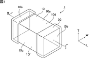
- FIG. 1 is a perspective view schematically showing an example of an electronic component according to an embodiment of the invention.
- FIG. 2 is a sectional view taken along line II-II in FIG.
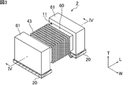
- FIG. 3 is a perspective view schematically showing another example of the electronic component according to the embodiment of the invention.
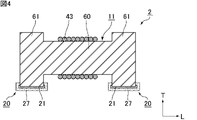
- FIG. 4 is a sectional view along line IV-IV in FIG.
- FIG. 5 is a cross-sectional view schematically showing an example of the state of the interface between the element body and the glass portion in one embodiment of the electronic component of the present invention.
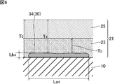
- FIG. 6 is a cross-sectional view schematically showing another example of the state of the interface between the element body and the glass portion in one embodiment of the electronic component of the present invention.
- FIG. 7 is a cross-sectional view schematically showing still another example of the state of the interface between the element body and the glass portion in one embodiment of the electronic component of the present invention.
- 8 is an elemental mapping image of Cu at the interface between the element body and the glass portion of the electronic component according to Example 2.
- FIG. 9 is an elemental mapping image of Si in the same field of view as in FIG.
- FIG. 10 is an image in which FIGS. 8 and 9 are superimposed.
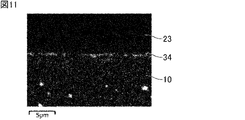
- 11 is an elemental mapping image of Cu at the interface between the element body and the glass portion of the electronic component according to Example 2.
- FIG. FIG. 12 is an elemental mapping image of Si in the same field of view as in FIG.
- the present invention is not limited to the following configurations, and can be appropriately modified and applied without changing the gist of the present invention.
- An embodiment of the electronic component of the present invention includes a ceramic element body containing Cu element, an external electrode covering a part of the surface of the element body, and a Cu segregation material containing Cu element, and the external electrode has a base electrode layer disposed on the base body, the base electrode layer has a conductor portion containing a conductor and a glass portion containing glass, and the Cu segregation is The interface between the base body and the glass portion is in contact with the base body and the glass portion.
- FIG. 1 is a perspective view schematically showing an example of an electronic component according to an embodiment of the invention.
- An electronic component 1 shown in FIG. 1 includes a base body 10 and external electrodes 20 covering part of the surface of the base body 10 .
- the element body 10 has a first end face 10a and a second end face 10b facing in the length direction L, a first side face 10c and a second side face 10d facing in the width direction W perpendicular to the length direction L, and a length direction L and a substantially rectangular parallelepiped shape having a top surface 10e and a bottom surface 10f facing each other in a thickness direction T orthogonal to the width direction W.
- the external electrodes 20 are provided so as to respectively cover the first end surface 10a and the second end surface 10b.
- a portion of the external electrode 20 covering the first end surface 10a is formed around a portion of the first side surface 10c, the second side surface 10d, the top surface 10e, and the bottom surface 10f of the element body 10.
- a portion of the external electrode 20 covering the second end surface 10b is formed around a portion of the first side surface 10c, the second side surface 10d, the top surface 10e, and the bottom surface 10f of the element body 10. As shown in FIG.
- FIG. 2 is a sectional view taken along line II-II in FIG.
- the element body 10 has a conductor layer 40 inside.
- the conductor layer 40 is exposed on the first end surface 10 a and the second end surface 10 b of the element body 10 and electrically connected to the external electrodes 20 .
- the conductor layer 40 forms a coil as a whole.
- the coil axis of the coil formed by the conductor layer 40 is parallel to the length direction L.
- the external electrode 20 has a base electrode layer 21 arranged on the element body 10 and a coating layer 27 arranged on the surface of the base electrode layer 21 .
- FIG. 3 is a perspective view schematically showing another example of the electronic component according to the embodiment of the invention.
- the electronic component 2 shown in FIG. 3 includes a base body 11 and external electrodes 20 covering part of the surface of the base body 11 .
- the shape of the element body 11 is a barbell shape having a columnar winding core portion 60 around which the winding wire 43 is wound and flange portions 61 connected to both ends of the winding core portion 60 in the length direction L, respectively.
- the winding 43 is wound around the winding core portion 60 of the element body 11 .
- the ends of the windings 43 are connected to the external electrodes 20 .
- FIG. 4 is a sectional view along line IV-IV in FIG. As shown in FIG. 4, no conductor layer is provided inside the element body 11 .
- the external electrode 20 has a base electrode layer 21 arranged on the element body 11 and a coating layer 27 arranged on the surface of the base electrode layer 21 .
- the element body is a ceramic containing Cu element.
- Ceramics containing Cu elements include, for example, known ceramics such as ferrite, alumina, barium titanate, and Zn-based ceramics containing Cu elements.
- the ceramic containing Cu element may contain additives such as Mn 3 O 4 , Co 3 O 4 , SnO 2 , Bi 2 O 3 and SiO 2 .
- the content of Cu element in the element is preferably 6 mol % or more and 10 mol % or less.
- the content of the Cu element in the element excludes from consideration the Cu element that constitutes the Cu segregation material segregated on the surface of the element.
- the content of Cu element in the element body is measured by wavelength dispersive X-ray fluorescence (WD-XRF) with a spot diameter of ⁇ 1 ⁇ m or more by exposing a cross section that is 10 ⁇ m or more inside the element body from the surface of the element body by polishing. Therefore, it is possible to measure as a value excluding the influence of segregation.
- the WD-XRF measurement may be performed on about five samples.
- the Fe element content in the element body is preferably 40 mol % or more and 49.5 mol % or less in terms of Fe 2 O 3 .
- Ni/Zn molar ratio in the element is not particularly limited, it is preferably 1.8 or more and 2.8 or less.
- the shape of the element is not particularly limited, and examples thereof include a cubic shape, a rectangular parallelepiped shape, a barbell shape, an H shape, an I shape, and an annular shape.
- the outer dimensions of the element are not particularly limited, but the smaller the element, the smaller the contact area between the element and the external electrodes. Become.
- the outer dimensions of the element are preferably length 5.7 mm or less x width 5.0 mm or less x height 5.0 mm or less, and length 1.6 mm or less x width 0.8 mm or less x height 0. 0.8 mm or less is particularly preferred.
- the element body may have a conductor layer inside.
- the conductor layers formed inside the element body may form passive elements such as coils, capacitors, resistors, and thermistors.
- a plurality of passive elements may be formed inside the base body.
- the orientation of the passive elements formed in the element body is arbitrary. Therefore, the coil axis of the coil formed in the base body may be horizontal or vertical to the mounting surface of the electronic component. Also, the number of coils formed in the element body may be one or plural.
- An example of the electronic component of the present invention in which a coil is formed in the element body is a laminated coil component. It may be a part or the like.
- the body may not have a conductor layer inside.
- the element can also be used as a winding core by winding a wire around it.
- An example of the electronic component of the present invention in which a wire is wound around the base includes a wound coil component.
- the number of coils formed by winding a wire around the element body may be one or plural.
- the external electrode In one embodiment of the electronic component of the present invention, the external electrode partially covers the surface of the element.
- the external electrode has a base electrode layer disposed on the element body.
- the underlying electrode layer has a conductor portion containing a conductor and a glass portion containing glass.
- the conductor portion plays a role of ensuring conductivity
- the glass portion plays a role of improving adhesion to the element body.
- the conductor portion may contain, as a conductor, at least one metal element selected from the group consisting of Ni, Sn, Pd, Au, Ag, Pt, Bi, Zn and Cu elements. preferable. Moreover, it is preferable to include conductive particles containing these metal elements.
- the conductor portion preferably contains Ag element as a conductor. Ag element has high conductivity. In addition, it is easy to form a base electrode layer containing a conductor containing Ag element as a conductor.
- the average particle size of the conductive particles is not particularly limited, it is preferably 1.0 ⁇ m or more and 15 ⁇ m or less.
- the weight ratio of the conductor part in the base electrode layer is not particularly limited, it is preferably 71% by weight or more and 98% by weight or less.
- glass examples include B--Si-based glass, Ba--B-Si-based glass, B--Si--Zn-based glass, B--Si--Zn--Ba-based glass, and B--Si--Zn--Ba-Ca--Al-based glass.
- alkali metal glasses such as Na—Si glasses, K—Si glasses, Li—Si glasses, Mg—Si glasses, Ca—Si glasses, Ba—Si glasses, Sr— Alkaline earth metal glass such as Si glass, Ti—Si glass, Zr—Si glass, Al—Si glass, and the like can also be used.
- the glass may be crystallizable glass.
- the weight ratio of the glass in the base electrode layer is not particularly limited, it is preferably 2% by weight or more and 15% by weight or less. When the weight ratio of the glass in the underlying electrode layer is 15% by weight or less, the resistance value of the underlying electrode layer does not become too large. Further, when the weight ratio of the glass in the underlying electrode layer is 2% by weight or more, the denseness of the underlying electrode layer can be increased, preventing the plating solution and moisture from penetrating into the underlying electrode layer and preventing the plating from entering. Liquid and moisture can be prevented from penetrating into the body through the base electrode layer.
- a coating layer may be further provided on the surface of the base electrode layer.
- the coating layer is preferably, for example, a plated layer provided on the surface of the underlying electrode layer.
- the plated layer preferably contains at least one metal selected from the group consisting of Cu, Ni, Sn, Pd, Au, Ag, Pt, Bi and Zn.
- the plating layer may be one layer, or two or more layers.
- the plating layer is more preferably a layer having a Ni plating layer and a Sn plating layer provided on the base electrode layer. The Ni-plated layer prevents water from entering the base body, and the Sn-plated layer can improve the mountability of the electronic component.
- the thickness of the external electrode is preferably 10 ⁇ m or more and 20 ⁇ m or less.
- the thickness of the underlying electrode layer is the thickness of the external electrode.
- the thickness of the external electrode is the sum of the thickness of the base electrode layer and the thickness of the coating layer.
- the thickness of the base electrode layer, the thickness of the coating layer, and the thickness of the external electrode can be measured by observing a cross section of the external electrode cut in the thickness direction with a scanning electron microscope (SEM). .
- SEM scanning electron microscope
- the Cu segregation containing Cu element is in contact with the element body and the glass portion at the interface between the element body and the glass portion.
- the presence of Cu segregation at the interface between the element and the glass increases the adhesion between the element and the glass.
- the Cu segregates may exist anywhere on the element, but preferably exist on the grain boundary of the ceramic of the element. Since the grain boundary of the ceramic of the element body has a concave shape on the surface of the element body, the presence of the Cu segregation on the grain boundary forming the concave shape causes an anchor effect, and the Cu segregation and The adhesion of the element is further improved.
- composition of the Cu segregation is not particularly limited, it may contain at least Cu element, and examples thereof include Cu, CuO, Cu 2 O, and the like. Also, the Cu segregants may contain glass.
- a plurality of Cu segregants may exist at the interface between the element body and the glass portion. If a plurality of Cu segregates exist at the interface between the element and the glass portion, the adhesion between the element and the glass portion can be further enhanced.
- Whether or not Cu segregation exists at the interface between the element body and the glass part is determined by scanning electron microscopy-energy dispersive X-ray spectroscopic analysis of the interface between the element body and the glass part on the cut surface obtained by cutting the electronic component. It can be confirmed by observing with (SEM-EDX). By confirming the concentration distribution of the Cu element from the elemental mapping image near the interface between the element body and the glass part obtained by SEM-EDX, the shape of the Cu segregation present near the interface between the element body and the glass part can be specified.
- the element body is ferrite
- the element body is mainly composed of Fe element
- the Cu segregation substance is mainly composed of Cu element
- the glass part of the base electrode layer is mainly composed of Si element.
- the elemental body, the Cu segregation matter, and the glass portion can be distinguished in the elemental mapping image.
- the element body is a ceramic other than ferrite
- concentrations of the elements that are the main components of the ceramic, the Cu element, and the Si element, the element, the Cu segregation, and the glass portion in the element mapping image can be determined. can be distinguished.
- Each element may be an element of the main component of the ceramic.
- the Cu segregation and the Cu plating layer can be distinguished by measuring the concentration distribution of the O element. Since the Cu plating layer is almost composed of pure Cu, the O element is hardly detected, whereas the O element derived from CuO and Cu 2 O is detected from the Cu segregation.
- the shape of the Cu segregates is not particularly limited, but may be granular, wedge-shaped, or layered.
- the shape of the Cu segregates can be determined by the value of the aspect ratio and whether or not the Cu segregates protrude toward the element body.
- the aspect ratio of the Cu segregation is defined as the length of the Cu segregation in the direction in which the interface between the element body and the glass portion extends, and the length of the Cu segregation in the direction orthogonal to La as Lb. It is represented by the ratio [La/Lb] of length La to Lb (hereinafter also referred to as aspect ratio).
- the length Lb passes through the point of the Cu segregation closest to the element body and the point farthest from the element body, and the interface between the element body and the glass portion extends. It corresponds to the distance between two line segments when each line segment is assumed to be parallel to the direction.
- the shape of the Cu segregation is wedge-shaped regardless of the aspect ratio of the Cu segregation.
- the shape with an aspect ratio of 3 or less is granular, and the shape with an aspect ratio of more than 3 is layered.
- the shape of the Cu segregation except for the portion protruding toward the element may be granular or layered. Note that the layered Cu segregation exists only in a portion of the interface between the element and the glass portion, and does not cover the entire interface between the element and the glass portion.
- FIG. 5 is a cross-sectional view schematically showing an example of the state of the interface between the element body and the glass portion in one embodiment of the electronic component of the present invention.
- the base electrode layer 21 has a glass portion 23 containing glass and a conductor portion 25 containing a conductor.
- FIG. 5 shows the glass portion 23 relatively large for explanation, the relative size relationship between the glass portion 23 and the conductor portion 25 is not limited to the structure shown in this drawing.
- FIG. 5 partially shows the base electrode layer 21, and there is a portion where the conductor part 25 is in contact with the base body 10 side, and the conductivity of the base electrode layer 21 as a whole is ensured.
- Cu segregants 30 are present at the interface between the element 10 and the glass portion 23, and are in contact with the element 10 and the glass portion 23.
- FIG. The thickness of the base electrode layer 21 in the portion where the Cu segregation 30 does not exist is the length indicated by the double arrow T0 . Note that the thickness T0 of the underlying electrode layer 21 may differ from place to place. In FIG. 5, it can be said that a plurality of Cu segregates are present at the interface between one glass portion 23 and the element body 10 .
- the Cu segregation 31 has a protruding portion 31a protruding toward the element body 10 side. Therefore, it can be said that the shape of the Cu segregants 31 is wedge-shaped regardless of the aspect ratio. Whether or not the Cu segregation protrudes toward the element body can be determined from the shape of the element surface at the portion where the Cu segregation does not exist on the surface of the element. Estimate the shape of the element surface when there is no substance, and when the Cu segregation is located inside (element side) the estimated element surface, the Cu segregation protrudes toward the element. assume that The Cu segregation may protrude toward the glass portion (underlying electrode layer) instead of toward the element body. However, the Cu segregation protruding only on the side of the glass portion, not on the side of the element body, is judged to have either a granular shape or a layered shape depending on the aspect ratio.
- the length of the Cu segregants 32 in the direction in which the interface between the base body 10 and the glass portion 23 extends is the length indicated by the double arrow La2.
- the length of the Cu segregants 32 in the direction orthogonal to the horizontal direction is the length indicated by the double arrow Lb2.
- the aspect ratio [La 2 /Lb 2 ] of the Cu segregants 32 is approximately 1.4. Therefore, the shape of the Cu segregants 32 is granular.
- the thickness of the Cu segregants 32 has a length indicated by a double -headed arrow Lb2, and the thickness of the underlying electrode layer 21 directly above and in contact with the Cu segregates 32 has a length indicated by a double -headed arrow T2. .
- the Cu segregation material 32 has a shape that does not protrude toward the element body 10 side.
- the sum of the thickness Lb 2 of the Cu segregants 32 and the thickness T 2 of the base electrode layer 21 directly in contact with the Cu segregates 32 matches the thickness T 0 of the base electrode layer 21 .
- the thickness T 0 of the base electrode layer 21 is thicker than the thickness T 2 of the base electrode layer 21 directly above and in contact with the Cu segregation 32 .
- the thickness T0 of the base electrode layer 21 is greater than the thickness T2 of the base electrode layer 21 directly in contact with the Cu segregants 32, the unevenness of the surface of the base electrode layer caused by the presence of the Cu segregates is small. As a result, the smoothness of the surface of the base electrode layer is improved.
- the Cu segregants 33 have a horizontal length of La 3 , a vertical length of Lb 3 , and an aspect ratio [La 3 /Lb 3 ] of about 1.9. Therefore, the shape of the Cu segregation 33 is granular.
- the thickness of the Cu segregants 33 is the length indicated by the double - headed arrow Lb3
- the thickness of the underlying electrode layer 21 directly above and in contact with the Cu segregates 33 is the length indicated by the double-headed arrow T3.
- the Cu segregation material 33 has a shape that does not protrude toward the element body 10 side. In FIG.
- the sum of the thickness Lb3 of the Cu segregants 33 and the thickness T3 of the base electrode layer 21 immediately above and in contact with the Cu segregates 33 coincides with the thickness T0 of the base electrode layer 21 .
- the thickness T0 of the base electrode layer 21 is thicker than the thickness T3 of the base electrode layer 21 directly above and in contact with the Cu segregation 33 .
- FIG. 6 is a cross-sectional view schematically showing another example of the state of the interface between the element body and the glass portion in one embodiment of the electronic component of the present invention.
- the Cu segregants 34 have a horizontal length indicated by a double-headed arrow La4 , and a vertical length indicated by a double-headed arrow Lb4 .
- the aspect ratio [La 4 /Lb 4 ] is about 10. Therefore, the shape of the Cu segregants 34 is layered. Note that the layered Cu segregation does not spread over the entire interface between the element and the glass portion, but only spreads over a portion of the interface between the element and the glass portion.
- the thickness of the Cu segregants 34 has a length indicated by a double-headed arrow Lb4
- the thickness of the base electrode layer 21 directly above and in contact with the Cu segregates 34 has a length indicated by a double - headed arrow T4.
- the Cu segregation material 34 has a shape that does not protrude toward the element body 10 side.
- the sum of the thickness Lb4 of the Cu segregants 34 and the thickness T4 of the base electrode layer 21 directly in contact with the Cu segregates 34 matches the thickness T0 of the base electrode layer 21 .
- the thickness T 0 of the base electrode layer 21 is thicker than the thickness T 4 of the base electrode layer 21 directly above and in contact with the Cu segregation 34 .
- the shape of the Cu segregates is related to the thickness of the glass portion directly above and in contact with the Cu segregates.
- the thickness of the glass portion directly above and in contact with the Cu segregation is less than 0.5 ⁇ m, the shape of the Cu segregation tends to be granular or wedge-shaped.
- the thickness of the glass portion directly contacting with the Cu segregants is 0.5 ⁇ m or more, the shape of the Cu segregates tends to be layered.
- the shape of the Cu segregation the part where the Cu segregation is mixed with the glass portion is also regarded as part of the Cu segregation. Therefore, the shape is specified as one Cu segregation including the portion where the Cu segregation is mixed with the glass portion. The boundary between the portion where the Cu segregation is mixed with the glass portion and the glass portion can be confirmed by element mapping of Si element and Cu element by SEM-EDX.
- the shape and aspect ratio of the Cu segregates, and the thickness of the glass portion immediately above and in contact with the Cu segregates can be measured by SEM-EDX.
- the shape and aspect ratio of Cu segregates are determined for each individual Cu segregate.
- the thickness of the glass portion directly above the Cu segregation is determined from the SEM-EDX image taken so that the Cu segregation and the glass portion are contained in one field of view. from a point on the upper surface of the glass part to a point on the top surface of the glass part directly above it in the vertical direction.
- the thickness of the glass portion 23 directly above and in contact with the Cu segregants 31 shown in FIG. 5 is the length indicated by the double arrow T1.
- the thickness of the glass portion 23 directly above and in contact with the Cu segregants 34 shown in FIG. 6 is the length indicated by the double arrow T5.
- the thickness of the underlying electrode layer that is in contact directly above the Cu segregation is determined by the Cu It is defined as the minimum value of the length from one point on the top surface of the segregation to one point on the top surface of the base electrode layer just above it in the vertical direction.
- the thickness of the base electrode layer in the portion where the Cu segregation does not exist is the average value of the lengths from the surface of the element body to the top surface of the base electrode layer measured at three points. For the above three points, visually select the point where the length from the surface of the element body to the top surface of the base electrode layer is the longest, the point where the length is the shortest, and the point where the length is between these.
- FIG. 7 is a cross-sectional view schematically showing still another example of the state of the interface between the element body and the glass portion in one embodiment of the electronic component of the present invention.
- a base electrode layer 21 is provided on the surface of the element body 10 shown in FIG.
- the base electrode layer 21 has a plurality of glass portions 23 ( 23 a, 23 b ) and conductor portions 25 .
- Cu segregates 30a and 30b are present at the interfaces between the plurality of glass portions 23a and 23b and the base body 10, respectively.
- the surface of the element body 10 has a portion not covered with the glass portion 23 , and this portion is covered with the conductor portion 25 .
- the Cu segregation 30c exists in the portion covered by the conductor portion 25 instead of the glass portion 23 .
- the conductor portion 25 exists directly above the Cu segregation material 30c.
- a plurality of glass portions exist in one base electrode layer, Cu segregation exists at the interface between one of the plurality of glass portions and the element body, and the remaining glass portions It can also be said that a Cu segregation containing Cu element exists at the interface between at least one of them and the element.
- An embodiment of the electronic component of the present invention may have an insulating film containing glass covering part of the surface of the element.
- the same glass as the glass forming the base electrode layer can be preferably used.
- the glass forming the insulating film and the glass forming the base electrode layer may be the same or different.
- Cu segregation may exist at the interface between the element and the insulating film.
- Cu segregation may also exist on the surface of the part of the element body that is not covered with the underlying electrode layer.
- the electronic component of this embodiment has excellent adhesion between the element body and the external electrodes.
- the electronic component of the present embodiment is not limited to a laminated coil component or a wound coil component, and may be any component as long as a ceramic containing Cu element is used as an element body.
- a first embodiment of the method for manufacturing an electronic component according to the present invention comprises a ceramic sheet preparation step of preparing a ceramic sheet formed by forming a ceramic raw material containing Cu element into a sheet shape, and forming conductor patterns to be via holes and coil patterns on the ceramic sheet.
- a step of forming a conductor pattern to be formed a step of preparing a laminate in which ceramic sheets are laminated, a step of firing the laminate to obtain a ceramic element, and a conductor portion including a conductor on the surface of the element.
- Ceramic sheet preparation process In the ceramic sheet preparation step, a ceramic raw material containing Cu element is formed into a sheet.
- the powdered ferrite raw material is prepared by weighing Fe 2 O 3 , ZnO, CuO, and NiO so as to have a predetermined ratio, wet-mixing them, and then pulverizing them. It can be obtained by drying and calcining.
- a ceramic slurry is prepared by mixing a ceramic raw material, an organic binder such as polyvinyl butyral resin, an organic solvent such as ethanol or toluene, and the like, and pulverizing the mixture.
- the ceramic slurry is formed into a sheet having a predetermined thickness by a doctor blade method or the like, and then punched into a predetermined shape to produce a ceramic sheet.
- the content of Cu element in the ceramic raw material is preferably 6 mol % or more and 10 mol % or less. The higher the content of Cu element in the ceramic raw material, the easier it is for Cu segregation to occur on the surface of the element.
- the content of the organic binder contained in the ceramic sheet is preferably 25% by weight or more and 35% by weight or less. Since the organic binder contained in the ceramic sheet contains carbon, it combines with oxygen in the atmosphere during firing to reduce the oxygen concentration. Therefore, as the content of the organic binder increases, the oxygen concentration tends to decrease in the firing process, and as a result, Cu segregation tends to occur on the surface of the element.
- the thickness of the ceramic sheet is not particularly limited, it is preferably 15 ⁇ m or more and 50 ⁇ m or less.
- a conductor pattern is formed by coating each ceramic sheet with a conductive paste such as Ag paste by a screen printing method or the like.
- a via hole is formed in advance by irradiating a predetermined portion of the ceramic sheet with a laser, and the via hole is filled with a conductive paste.
- Laminate preparation step After laminating the ceramic sheets, a laminated body is produced by crimping them by warm isostatic pressing (WIP) or the like.
- WIP warm isostatic pressing
- the number of laminated ceramic sheets is not particularly limited, it is preferably 30 or more and 100 or less.
- the laminate is sintered to obtain an element body.
- the firing conditions are such that Cu segregation derived from Cu in the element is deposited on the surface of the element. Whether or not Cu segregation occurs on the surface of the element body depends not only on the composition of the ceramic raw material, but also on the amount of carbon contained in the laminate, the firing temperature (maximum temperature), the rate of temperature increase, the firing atmosphere, the material of the firing furnace, etc. affects. When these conditions are appropriately selected, Cu segregates are precipitated on the surface of the element. That is, if the firing conditions are not appropriate, Cu segregation will not precipitate on the surface of the element even if the composition of the ceramic raw material is the same.
- the firing temperature (maximum temperature) in the firing step is preferably 1000° C. or higher and 1300° C. or lower. If the firing temperature (maximum temperature) in the firing step is 1000° C. or higher, Cu segregation is likely to occur on the surface of the element.
- the oxygen concentration in the firing step is preferably 15% by volume or less, more preferably 5% by volume or less. If the oxygen content in the firing atmosphere is 15% by volume or less, Cu segregation is likely to occur on the surface of the element.
- the balance gas in the firing step is preferably nitrogen or argon.
- the heating rate in the firing step is preferably 10° C./min or less. The shorter the time it takes to reach the sintering temperature, the more easily Cu segregation occurs on the surface of the element.
- the furnace material that constitutes the firing furnace for firing the laminate in the firing step is preferably a high-density material such as a mixture of alumina and silicon. If the furnace material that constitutes the firing furnace is made of a high-density material, Cu segregation is likely to occur.
- Base electrode layer forming step a base electrode layer having a conductor portion containing a conductor and a glass portion containing glass is formed on the surface of the element body obtained by the firing step.
- the base electrode layer can be formed by applying a paste containing conductive particles and glass (hereinafter referred to as glass paste) to the surface of the element and firing (baking) it.
- glass paste may contain a resin and a dispersion medium in addition to the conductive particles and the glass.
- conductive particles conductive particles containing at least one metal element selected from the group consisting of Ni elements, Sn elements, Pd elements, Au elements, Ag elements, Pt elements, Bi elements, Zn elements and Cu elements. is mentioned.
- the average particle size of the conductive particles is not particularly limited, it is preferably 0.5 ⁇ m or more and 10 ⁇ m or less. As the average particle size of the conductive particles constituting the glass paste increases, the number of voids in the glass paste before sintering increases, and the thickness of the base electrode layer tends to decrease due to baking. Therefore, granular or wedge-shaped Cu segregates are likely to be formed. On the other hand, the smaller the average particle diameter of the conductive particles constituting the glass paste, the fewer the voids in the glass paste before sintering, and the more likely the base electrode layer will be thickened by baking. Therefore, a layered Cu segregation is likely to be formed.
- glass examples include B--Si-based glass, Ba--B-Si-based glass, B--Si--Zn-based glass, B--Si--Zn--Ba-based glass, and B--Si--Zn--Ba-Ca--Al-based glass.
- alkali metal glasses such as Na—Si glasses, K—Si glasses, Li—Si glasses, Mg—Si glasses, Ca—Si glasses, Ba—Si glasses, Sr— Alkaline earth metal glass such as Si glass, Ti—Si glass, Zr—Si glass, Al—Si glass, and the like can also be used.
- the glass may be crystallizable glass.
- the average particle size of the glass constituting the glass paste is not particularly limited, it is preferably 0.5 ⁇ m or more and 10 ⁇ m or less.
- the temperature (baking temperature) for baking the glass paste is not particularly limited, but is preferably 750° C. or higher and 900° C. or lower.
- the baking temperature is 750° C. or higher and 900° C. or lower, Cu segregation is more likely to occur on the surface of the element.
- the Cu segregation and the glass contained in the glass portion of the base electrode layer can easily form a mixture, and the adhesion between the element and the base electrode layer can be improved.
- baking is preferably performed in a non-oxidizing atmosphere. By performing the baking at 825° C. or higher in a non-oxidizing atmosphere, the segregation of Cu on the surface of the element body can be promoted. Therefore, the adhesion between the element body and the base electrode layer can be further improved.
- Examples of resins contained in the glass paste include polyvinyl butyral resins.
- the content of the resin contained in the glass paste is preferably 20% by weight or more and 30% by weight or less. When the content of the resin contained in the glass paste is within the above range, the segregation of Cu on the surface of the element body can be promoted.
- the coating layer is preferably a plated layer formed by plating.
- the plated layer preferably contains at least one metal selected from the group consisting of Cu, Ni, Sn, Pd, Au, Ag, Pt, Bi and Zn.
- the plating layer may be one layer, or two or more layers.
- the plating layer is more preferably a layer having a Ni plating layer and a Sn plating layer provided on the base electrode layer. Heating may be further performed after the plating layer is formed.
- the method for manufacturing the base body may be a method other than the sheet lamination method described above.
- Methods other than the sheet lamination method include, for example, a print lamination method (build-up method).
- a method using photolithography can also be used as a method for forming wiring and vias on the surface of the sheet.
- a second embodiment of the method for manufacturing an electronic component according to the present invention includes an element preparation step of forming a ceramic raw material containing Cu element to prepare a ceramic element containing Cu element, and a conductor on the surface of the element. It includes a step of forming a base electrode layer having a conductive portion and a glass portion containing glass, and a step of forming a coil of winding a wire to be a coil on the surface of the element body.
- the same ceramic raw material as used in the first embodiment of the method for manufacturing an electronic component according to the present invention can be preferably used.
- a method for molding the ceramic raw material into a predetermined shape a conventionally known powder molding method can be used. At this time, a resin, a binder, or the like may be added to the ceramic raw material, if necessary. A body is obtained by firing a molded body obtained by molding a ceramic raw material. At this time, the compact is fired under the conditions that Cu segregation occurs on the surface of the element.
- the element obtained by the above method is an element containing no conductor layer inside.
- the base electrode layer forming step in the second embodiment of the electronic component manufacturing method of the present invention is the same as the base electrode layer forming step in the first embodiment of the electronic component manufacturing method of the present invention.
- a wire that forms a coil is wound around the surface of the element body, and both ends of the coil are connected to external electrodes.
- the method of connecting the windings to be the coil and the external electrodes is not particularly limited, for example, a method of bonding by thermocompression bonding can be used.
- the number of winding turns (number of turns) and the diameter of the winding may be appropriately changed according to the specifications required for the electronic component.
- Example 1 [Body preparation process] A ferrite raw material prepared so that the Fe content is constant, the Ni/Zn molar ratio is 2.3, and the Cu content is 8 mol%, is shaped into a barbell shape having a winding portion and a flange portion. A compact was obtained by molding.
- a ceramic body was obtained by firing the compact at 1100° C. for 1 hour.
- the atmosphere during firing was normal pressure and oxygen partial pressure was 10% by volume.
- Example 1 A glass paste was prepared by mixing a mixture of glass frit (borosilicate glass) and Ag particles at a ratio of 5:95 (weight ratio) and a solvent, and the glass paste was applied to the surface of the body obtained in the firing process. , and baking at 650° C. for 40 minutes to form a base electrode layer, plating the surface of the base electrode layer, forming a Ni plating layer as a coating layer, and manufacturing an electronic component according to Example 1. Since the segregation amount of Cu segregation is likely to occur as the baking temperature increases, the baking temperature is preferably 750° C. or higher. By setting the temperature to 850° C. or higher, the fluidity of the Cu segregation itself is improved.
- Example 2 Comparative Examples 1 to 3
- Example 2 was carried out in the same manner as in Example 1, except that the Cu content was changed to 6 mol%, 4 mol%, 1 mol%, and 0 mol% without changing the Fe content and Ni/Zn molar ratio in the ferrite raw material.
- electronic parts according to Comparative Examples 1 to 3 were manufactured.
- the sintered densities of the bodies of each example and comparative example were about the same as that of the first example.
- Comparative Example 4 An electronic component according to Comparative Example 4 was manufactured in the same manner as in Example 1 except that the firing temperature (maximum temperature) of the compact was changed to 950° C. or less without changing the composition of the ferrite raw material.
- the sintered density of the element body of Comparative Example 4 was about the same as that of Example 1.
- FIG. 8 is an elemental mapping image of Cu at the interface between the element body and the glass portion of the electronic component according to Example 2
- FIG. 9 is an elemental mapping image of Si in the same field of view as FIG. is an image in which FIGS. 8 and 9 are superimposed.
- regions with high Cu concentration (Cu segregants 31, 32, 33) exist at the interface between the element body 10 and the glass portion 23. I confirmed that Wedge-shaped Cu segregants 31 are present on the left sides of FIGS. I have verified that it exists.
- the thickness of the glass portion 23 directly above and in contact with the wedge-shaped Cu segregation 31 shown in FIGS. 8, 9 and 10 was 0.4 ⁇ m.
- the aspect ratios of the granular Cu segregates 32 and 33 shown in FIGS. 8, 9 and 10 were about 1.2-1.9, all of which were 3 or less. Further, the thickness of the glass portion 23 directly above and in contact with the granular Cu segregants 32 was 0.3 ⁇ m.
- FIG. 11 is an elemental mapping image of Cu at the interface between the element body and the glass portion of the electronic component according to Example 2
- FIG. 12 is an elemental mapping image of Si in the same field of view as in FIG.
- the positions for measuring SEM-EDX in FIGS. 11 and 12 are different from the positions for measuring SEM-EDX in FIGS. From the results of FIG. 11, it was confirmed that in the electronic component according to Example 2, a region of high Cu concentration (Cu segregation 34) was present at the interface between the element body 10 and the glass portion 23. In FIG. 11 , there are discontinuous portions along the interface between the element body 10 and the underlying electrode layer 21 for the white dots indicating the high Cu concentration. According to the Si elemental mapping of SEM-EDX shown in FIG.
- the Si concentration in this portion is lower than that of the base electrode layer 21, and it is considered that the Cu segregation includes the glass constituting the base electrode layer 21. be done. That is, at the interface between the element body 10 and the underlying electrode layer 21 shown in FIGS. It can be said that the entire Cu segregation is layered. The aspect ratio of this layered Cu segregate 34 exceeded 3, and the thickness of the glass portion 23 directly above and in contact with the Cu segregate 34 was 5 ⁇ m or more. From the results of FIGS. 8, 9, 10, 11 and 12, it was confirmed that a plurality of Cu segregants with different shapes existed at the interface between the glass portion and the element body in the same electronic component. did.
- the electronic components according to the embodiments of the present invention can be suitably used as components such as inductors, antennas, noise filters, radio wave absorbers, and LC filters combined with capacitors.
- Reference Signs List 1 2 Electronic component 10, 11 Element body 10a First end face of element body 10b Second end face of element body 10c First side face of element body 10d Second side face of element body 10e Upper surface of element body 10f Bottom surface of element body 20 Outside Electrode 21 Underlying electrode layer 23, 23a, 23b Glass portion 25 Conductor 27 Coating layer 30, 30a, 30b, 30c, 31, 32, 33, 34 Cu segregation 31a Protruding portion 40 in which Cu segregation protrudes toward the element body Conductor layer 43 Winding 60 Winding core 61 Flange L Length direction La 2 , La 3 , La 4 Horizontal length of Cu segregation Lb 2 , Lb 3 , Lb 4 Length of Cu segregation T Thickness direction T 0 Thickness of base electrode layer T 1 , T 5 Thickness of glass part directly in contact with Cu segregate T 2 , T 3 , T 4 Thickness of base electrode layer directly in contact with Cu segregate W width direction
Landscapes
- Engineering & Computer Science (AREA)
- Power Engineering (AREA)
- Microelectronics & Electronic Packaging (AREA)
- Coils Or Transformers For Communication (AREA)
- Ceramic Capacitors (AREA)
- Fixed Capacitors And Capacitor Manufacturing Machines (AREA)
Priority Applications (4)
| Application Number | Priority Date | Filing Date | Title |
|---|---|---|---|
| CN202180089179.0A CN116724367A (zh) | 2021-02-01 | 2021-12-07 | 电子部件 |
| JP2022578102A JP7491411B2 (ja) | 2021-02-01 | 2021-12-07 | 電子部品 |
| DE212021000512.8U DE212021000512U1 (de) | 2021-02-01 | 2021-12-07 | Elektronisches Bauteil |
| US18/355,821 US20230360843A1 (en) | 2021-02-01 | 2023-07-20 | Electronic component |
Applications Claiming Priority (2)
| Application Number | Priority Date | Filing Date | Title |
|---|---|---|---|
| JP2021-014488 | 2021-02-01 | ||
| JP2021014488 | 2021-02-01 |
Related Child Applications (1)
| Application Number | Title | Priority Date | Filing Date |
|---|---|---|---|
| US18/355,821 Continuation US20230360843A1 (en) | 2021-02-01 | 2023-07-20 | Electronic component |
Publications (1)
| Publication Number | Publication Date |
|---|---|
| WO2022163140A1 true WO2022163140A1 (ja) | 2022-08-04 |
Family
ID=82653316
Family Applications (1)
| Application Number | Title | Priority Date | Filing Date |
|---|---|---|---|
| PCT/JP2021/044963 Ceased WO2022163140A1 (ja) | 2021-02-01 | 2021-12-07 | 電子部品 |
Country Status (5)
| Country | Link |
|---|---|
| US (1) | US20230360843A1 (https=) |
| JP (1) | JP7491411B2 (https=) |
| CN (1) | CN116724367A (https=) |
| DE (1) | DE212021000512U1 (https=) |
| WO (1) | WO2022163140A1 (https=) |
Citations (3)
| Publication number | Priority date | Publication date | Assignee | Title |
|---|---|---|---|---|
| JP2005317748A (ja) * | 2004-04-28 | 2005-11-10 | Tdk Corp | 複合電子部品及びその製造方法 |
| WO2011013437A1 (ja) * | 2009-07-31 | 2011-02-03 | 株式会社村田製作所 | 積層コイル部品 |
| JP2018098372A (ja) * | 2016-12-14 | 2018-06-21 | 株式会社村田製作所 | セラミック電子部品及びその製造方法 |
Family Cites Families (4)
| Publication number | Priority date | Publication date | Assignee | Title |
|---|---|---|---|---|
| JP5217659B2 (ja) * | 2008-06-10 | 2013-06-19 | 株式会社村田製作所 | セラミック電子部品、およびセラミック電子部品の製造方法 |
| JP6015221B2 (ja) * | 2012-08-07 | 2016-10-26 | 株式会社村田製作所 | セラミック電子部品の製造方法 |
| JP6914617B2 (ja) | 2016-05-11 | 2021-08-04 | Tdk株式会社 | 積層コイル部品 |
| KR102625407B1 (ko) * | 2019-05-24 | 2024-01-16 | 가부시키가이샤 무라타 세이사쿠쇼 | 전자부품, 및 규산염 피막의 형성 방법 |
-
2021
- 2021-12-07 JP JP2022578102A patent/JP7491411B2/ja active Active
- 2021-12-07 DE DE212021000512.8U patent/DE212021000512U1/de active Active
- 2021-12-07 WO PCT/JP2021/044963 patent/WO2022163140A1/ja not_active Ceased
- 2021-12-07 CN CN202180089179.0A patent/CN116724367A/zh active Pending
-
2023
- 2023-07-20 US US18/355,821 patent/US20230360843A1/en active Pending
Patent Citations (3)
| Publication number | Priority date | Publication date | Assignee | Title |
|---|---|---|---|---|
| JP2005317748A (ja) * | 2004-04-28 | 2005-11-10 | Tdk Corp | 複合電子部品及びその製造方法 |
| WO2011013437A1 (ja) * | 2009-07-31 | 2011-02-03 | 株式会社村田製作所 | 積層コイル部品 |
| JP2018098372A (ja) * | 2016-12-14 | 2018-06-21 | 株式会社村田製作所 | セラミック電子部品及びその製造方法 |
Also Published As
| Publication number | Publication date |
|---|---|
| JP7491411B2 (ja) | 2024-05-28 |
| DE212021000512U1 (de) | 2023-08-22 |
| CN116724367A (zh) | 2023-09-08 |
| US20230360843A1 (en) | 2023-11-09 |
| JPWO2022163140A1 (https=) | 2022-08-04 |
Similar Documents
| Publication | Publication Date | Title |
|---|---|---|
| US9741484B2 (en) | Laminated coil component | |
| KR101421453B1 (ko) | 적층 부품 | |
| CN107017081B (zh) | 层叠电感器 | |
| US9165705B2 (en) | Laminated inductor | |
| CN112614697A (zh) | 层叠陶瓷电容器 | |
| KR101842341B1 (ko) | 코일 부품 | |
| US20130038419A1 (en) | Laminated inductor | |
| US10290415B2 (en) | Electronic component and manufacturing method therefor | |
| CN108878142A (zh) | 层叠陶瓷电容器 | |
| JP2012238840A (ja) | 積層インダクタ | |
| JP2008177611A (ja) | 表面実装型負特性サーミスタ | |
| US20240371571A1 (en) | Multilayer ceramic capacitor | |
| JP2010183025A (ja) | 積層セラミックコンデンサ | |
| KR101215923B1 (ko) | 적층 코일 부품 및 그 제조 방법 | |
| JP7552739B2 (ja) | 電子部品 | |
| JP7491411B2 (ja) | 電子部品 | |
| US6370014B1 (en) | Monolithic ceramic electronic component and method for manufacturing the same | |
| JP6902069B2 (ja) | インダクタ | |
| JP6553279B2 (ja) | 積層インダクタ | |
| JP6544485B2 (ja) | セラミック電子部品及びセラミック電子部品の製造方法 | |
| JP4387150B2 (ja) | 積層セラミック電子部品およびその製造方法 | |
| JPH0795630B2 (ja) | 複合積層セラミック部品 | |
| US20240145141A1 (en) | Magnetic base body, coil component including the magnetic base body, circuit board including the coil component, and electronic device including the circuit board | |
| JP3164664B2 (ja) | 多層回路基板 | |
| JP2024077239A (ja) | 積層型コイル部品及び積層型コイル部品の製造方法 |
Legal Events
| Date | Code | Title | Description |
|---|---|---|---|
| 121 | Ep: the epo has been informed by wipo that ep was designated in this application |
Ref document number: 21923145 Country of ref document: EP Kind code of ref document: A1 |
|
| ENP | Entry into the national phase |
Ref document number: 2022578102 Country of ref document: JP Kind code of ref document: A |
|
| WWE | Wipo information: entry into national phase |
Ref document number: 202180089179.0 Country of ref document: CN |
|
| WWE | Wipo information: entry into national phase |
Ref document number: 212021000512 Country of ref document: DE |
|
| 122 | Ep: pct application non-entry in european phase |
Ref document number: 21923145 Country of ref document: EP Kind code of ref document: A1 |