WO2022158594A1 - フィルム状接着剤及び接続構造体の製造方法 - Google Patents
フィルム状接着剤及び接続構造体の製造方法 Download PDFInfo
- Publication number
- WO2022158594A1 WO2022158594A1 PCT/JP2022/002460 JP2022002460W WO2022158594A1 WO 2022158594 A1 WO2022158594 A1 WO 2022158594A1 JP 2022002460 W JP2022002460 W JP 2022002460W WO 2022158594 A1 WO2022158594 A1 WO 2022158594A1
- Authority
- WO
- WIPO (PCT)
- Prior art keywords
- film
- adhesive
- mass
- electrode
- component
- Prior art date
- Legal status (The legal status is an assumption and is not a legal conclusion. Google has not performed a legal analysis and makes no representation as to the accuracy of the status listed.)
- Ceased
Links
Images


Classifications
-
- C—CHEMISTRY; METALLURGY
- C09—DYES; PAINTS; POLISHES; NATURAL RESINS; ADHESIVES; COMPOSITIONS NOT OTHERWISE PROVIDED FOR; APPLICATIONS OF MATERIALS NOT OTHERWISE PROVIDED FOR
- C09J—ADHESIVES; NON-MECHANICAL ASPECTS OF ADHESIVE PROCESSES IN GENERAL; ADHESIVE PROCESSES NOT PROVIDED FOR ELSEWHERE; USE OF MATERIALS AS ADHESIVES
- C09J11/00—Features of adhesives not provided for in group C09J9/00, e.g. additives
- C09J11/02—Non-macromolecular additives
- C09J11/04—Non-macromolecular additives inorganic
-
- C—CHEMISTRY; METALLURGY
- C09—DYES; PAINTS; POLISHES; NATURAL RESINS; ADHESIVES; COMPOSITIONS NOT OTHERWISE PROVIDED FOR; APPLICATIONS OF MATERIALS NOT OTHERWISE PROVIDED FOR
- C09J—ADHESIVES; NON-MECHANICAL ASPECTS OF ADHESIVE PROCESSES IN GENERAL; ADHESIVE PROCESSES NOT PROVIDED FOR ELSEWHERE; USE OF MATERIALS AS ADHESIVES
- C09J11/00—Features of adhesives not provided for in group C09J9/00, e.g. additives
- C09J11/02—Non-macromolecular additives
- C09J11/06—Non-macromolecular additives organic
-
- C—CHEMISTRY; METALLURGY
- C09—DYES; PAINTS; POLISHES; NATURAL RESINS; ADHESIVES; COMPOSITIONS NOT OTHERWISE PROVIDED FOR; APPLICATIONS OF MATERIALS NOT OTHERWISE PROVIDED FOR
- C09J—ADHESIVES; NON-MECHANICAL ASPECTS OF ADHESIVE PROCESSES IN GENERAL; ADHESIVE PROCESSES NOT PROVIDED FOR ELSEWHERE; USE OF MATERIALS AS ADHESIVES
- C09J4/00—Adhesives based on organic non-macromolecular compounds having at least one polymerisable carbon-to-carbon unsaturated bond ; adhesives, based on monomers of macromolecular compounds of groups C09J183/00 - C09J183/16
-
- C—CHEMISTRY; METALLURGY
- C09—DYES; PAINTS; POLISHES; NATURAL RESINS; ADHESIVES; COMPOSITIONS NOT OTHERWISE PROVIDED FOR; APPLICATIONS OF MATERIALS NOT OTHERWISE PROVIDED FOR
- C09J—ADHESIVES; NON-MECHANICAL ASPECTS OF ADHESIVE PROCESSES IN GENERAL; ADHESIVE PROCESSES NOT PROVIDED FOR ELSEWHERE; USE OF MATERIALS AS ADHESIVES
- C09J7/00—Adhesives in the form of films or foils
- C09J7/30—Adhesives in the form of films or foils characterised by the adhesive composition
-
- C—CHEMISTRY; METALLURGY
- C09—DYES; PAINTS; POLISHES; NATURAL RESINS; ADHESIVES; COMPOSITIONS NOT OTHERWISE PROVIDED FOR; APPLICATIONS OF MATERIALS NOT OTHERWISE PROVIDED FOR
- C09J—ADHESIVES; NON-MECHANICAL ASPECTS OF ADHESIVE PROCESSES IN GENERAL; ADHESIVE PROCESSES NOT PROVIDED FOR ELSEWHERE; USE OF MATERIALS AS ADHESIVES
- C09J9/00—Adhesives characterised by their physical nature or the effects produced, e.g. glue sticks
- C09J9/02—Electrically-conducting adhesives
-
- H—ELECTRICITY
- H05—ELECTRIC TECHNIQUES NOT OTHERWISE PROVIDED FOR
- H05K—PRINTED CIRCUITS; CASINGS OR CONSTRUCTIONAL DETAILS OF ELECTRIC APPARATUS; MANUFACTURE OF ASSEMBLAGES OF ELECTRICAL COMPONENTS
- H05K1/00—Printed circuits
- H05K1/02—Details
- H05K1/14—Structural association of two or more printed circuits
-
- H—ELECTRICITY
- H05—ELECTRIC TECHNIQUES NOT OTHERWISE PROVIDED FOR
- H05K—PRINTED CIRCUITS; CASINGS OR CONSTRUCTIONAL DETAILS OF ELECTRIC APPARATUS; MANUFACTURE OF ASSEMBLAGES OF ELECTRICAL COMPONENTS
- H05K3/00—Apparatus or processes for manufacturing printed circuits
- H05K3/30—Assembling printed circuits with electric components, e.g. with resistors
- H05K3/32—Assembling printed circuits with electric components, e.g. with resistors electrically connecting electric components or wires to printed circuits
-
- C—CHEMISTRY; METALLURGY
- C08—ORGANIC MACROMOLECULAR COMPOUNDS; THEIR PREPARATION OR CHEMICAL WORKING-UP; COMPOSITIONS BASED THEREON
- C08K—Use of inorganic or non-macromolecular organic substances as compounding ingredients
- C08K2201/00—Specific properties of additives
- C08K2201/001—Conductive additives
Definitions
- This specification relates to a method for manufacturing a film adhesive and a connection structure.
- FPC/FPC connection via film adhesive has been used as a component for terminals such as organic EL elements (OLED), liquid crystal display terminals (smartphones, tablets, smartwatches, etc.), wearable terminals (terminals worn on the body), etc.
- terminals such as organic EL elements (OLED), liquid crystal display terminals (smartphones, tablets, smartwatches, etc.), wearable terminals (terminals worn on the body), etc.
- COF FPC/FPC connections, FPC/PWB connections, or COF FPC/PWB connections have been used.
- These connection structures are required to have a low connection resistance in order to improve display quality and reduce power consumption.
- a film-like adhesive that can be mounted at a lower pressure (for example, 1 MPa or less).
- the main object of the present invention is to provide a film-like adhesive for circuit connection, which is capable of obtaining a connection structure exhibiting low connection resistance even in low-pressure mounting.
- One aspect of the present invention relates to a film-like adhesive for circuit connection shown in [1] below.
- a film adhesive for circuit connection comprising solder particles having a Bi content of 20 to 60% by mass and an Sn content of 40 to 80% by mass, a radically polymerizable compound, and thermal radicals and a generator, wherein the average particle size of the solder particles is 0.5 to 1.5 times the thickness of the film adhesive.
- connection structure obtained by the film-like adhesive on the side surface tends to be able to exhibit excellent display quality and reduce power consumption.
- the inventors presume the reason why the above effects are obtained as follows.
- the electrical connection between the members is performed by limited physical contact between the conductive particle surface and the electrode surface, whereas the film adhesive of the side surface .
- the solder particles of the above specific composition in addition to the close and extensive physical contact between the electrode surface and the solder particle surface, the metal element of the solder and the metal element on the outermost surface of the electrode plating can form a mixed layer (metal bonding by intermetallic compound).
- the average particle diameter of the solder particles is 0.5 times or more the thickness of the film-like adhesive, so that the amount of the adhesive component necessary for capturing the solder particles is reduced. Since the amount of flow is small, solder particles can be captured even in low-pressure mounting. For these reasons, it is presumed that the above-mentioned effect can be obtained with the film-like adhesive of the above aspect.
- connection structure is required to have high connection reliability that can maintain a low connection resistance even in a high-temperature and high-humidity environment.
- connection structure obtained by the film-like adhesive on the side surface tends to show stable and low connection resistance even after the high-temperature and high-humidity environment test, and can maintain excellent display quality even in severe environments. They tend to have high reliability.
- solder particles with the above composition tend to have a softening point at a low temperature (eg, 130 to 180°C). Therefore, according to the film-like adhesive of the side surface, even when mounting is performed at a low temperature, there is a tendency to obtain a connection structure exhibiting low connection resistance.
- the film-like adhesive on the side surface may be the film-like adhesive shown in [2] to [4] below.
- a surface of a first circuit member having a first electrode on which the first electrode is provided and a surface of a second circuit member having a second electrode on which the second circuit member has the second electrode are provided.
- the first electrode and the second electrode are electrically connected to each other and the first circuit member and the second electrode are electrically connected to each other by thermocompression bonding at a pressure of 1 MPa or less through the film adhesive. and bonding two circuit members together.
- the first electrode is an electrode having an Au plating layer on the outermost surface
- the second electrode is an electrode having an Au plating layer or an Sn plating layer on the outermost surface.
- a film-like adhesive for circuit connection which is capable of obtaining a connection structure exhibiting low connection resistance even in low-pressure mounting.
- FIG. 1 is a schematic cross-sectional view showing a film adhesive of one embodiment.
- FIG. 2 is a schematic cross-sectional view showing a film adhesive according to another embodiment.
- FIG. 3 is a schematic cross-sectional view showing a connection structure according to one embodiment.
- 4A to 4D are schematic cross-sectional views showing a method of manufacturing the connection structure of FIG.
- (meth)acrylate means at least one of acrylate and its corresponding methacrylate.
- the materials exemplified below may be used singly or in combination of two or more unless otherwise specified.
- the content of each component in the composition means the total amount of the plurality of substances present in the composition unless otherwise specified when there are multiple substances corresponding to each component in the composition.
- a numerical range indicated using “-” indicates a range including the numerical values before and after "-" as the minimum and maximum values, respectively.
- “A or B” may include either A or B, or may include both.
- “Normal temperature” means 25° C.
- “normal pressure” means 1 atm.
- the upper limit or lower limit of the numerical range at one stage may be replaced with the upper limit or lower limit of the numerical range at another stage.
- the upper and lower limits of the numerical ranges may be replaced with the values shown in the examples.
- the present invention provides a film adhesive for circuit connection. Moreover, in one aspect, the present invention provides application of a film-like adhesive or a cured product thereof to a connection structure or its manufacture. Moreover, in one aspect, the present invention provides application of a film-like adhesive or a cured product thereof to circuit connection. Moreover, this invention provides the application of the connection structure to a wearable use in one aspect.
- the film adhesive of one embodiment comprises solder particles having a Bi content of 20 to 60% by mass and an Sn content of 40 to 80% by mass, a radically polymerizable compound, and a thermal radical generator. and the average particle diameter of the solder particles is 0.5 to 1.5 times the thickness of the film adhesive for circuit connection.
- the film adhesive may have a curing point at a temperature lower than the softening point of the solder particles.
- the viscosity of the film-like adhesive at the softening point of the solder particles may be 3 times or more of the minimum melt viscosity.
- the softening point of the solder particles may be 130-180.degree.
- FIG. 1 is a schematic cross-sectional view showing a film adhesive according to one embodiment.
- the film adhesive 1 shown in FIG. 1 is an adhesive for circuit connection, and includes (A) solder particles 2 having a Bi content of 20 to 60% by mass and an Sn content of 40 to 80% by mass ( (hereinafter also referred to as “(A) component”), (B) radical polymerizable compound (hereinafter also referred to as “(B) component”), and (C) thermal radical generator (hereinafter referred to as “(C) component”) Also referred to as ) and .
- adhesive components other than component (A) contained in film adhesive 1 are referred to as adhesive components.
- component (A) component solder particles
- Component (A) contains 20 to 60% by mass of Bi (bismuth) and 40 to 80% by mass of Sn (tin). If the composition of Bi and Sn is within the above range, the liquid solder component melted at around 139° C. and the solid solder component will coexist during thermocompression bonding. Solder particles wet and spread on the surface, making it possible to form close and extensive physical contact and partial metallic bonding (a layer in which the metallic element of the solder and the metallic element on the outermost surface of the electrode plating are mixed). From the viewpoint of facilitating the formation of such metal joints, the component (A) may be solder particles having a Bi content of 21 to 58% by mass and an Sn content of 42 to 79% by mass. The solder particles may have a Sn content of 21 to 40% by mass and a Sn content of 60 to 79% by mass.
- the (A) component may further contain other metal elements as long as the Bi content and Sn content are within the ranges described above.
- Other metal elements include common metal elements that can be included in solder.
- the metal elements contained in the component (A) may be only Bi and Sn.
- the connection structure exhibits lower connection resistance and higher connection reliability. is easy to obtain.
- the softening point of component (A) is, for example, 130 to 180°C.
- the softening point of component (A) may be 170° C. or lower, 160° C. or lower, 150° C. or lower, or 140° C. or lower from the viewpoint of enabling low-temperature mounting.
- the softening point of component (A) may be 135° C. or higher from the viewpoint of further improving the trapping property of solder particles. From these viewpoints, the softening point of component (A) may be 130 to 170°C, 130 to 160°C, 130 to 150°C or 130 to 140°C, 135 to 170°C, 135 to 160°C, 135 ⁇ 150°C or 135-140°C.
- the softening point of the component can be measured using a DSC (differential scanning calorimeter). Specifically, when DSC measurement of component (A) is performed in He gas flow at a heating rate of 10 ° C./min, the first endothermic peak (first endothermic peak) of component (A) is Softening point.
- DSC differential scanning calorimeter
- the average particle size of the component (A) is 0.5 to 1.5 times the thickness of the film adhesive 1.
- the average particle diameter of the component (A) is 0% of the thickness of the film-like adhesive 1 from the viewpoint of being able to further improve the ability to capture solder particles and to obtain a connection structure exhibiting a lower connection resistance. It is preferably 0.6 times or more, and may be 0.7 times or more or 0.8 times or more.
- the average particle size of the component (A) is 1.3 times or less, 1.2 times or less, or 1.1 times or less the thickness of the film adhesive 1 from the viewpoint of the ease of the manufacturing method and the manufacturing stability. It may be 1.0 times or less, 0.9 times or less, or 0.8 times or less.
- the average particle diameter of the component (A) is 0.5 to 1.3 times, 0.5 to 1.2 times, and 0.5 to 1.1 times the thickness of the film adhesive 1. , 0.5-1.0 times, 0.5-0.9 times, 0.5-0.8 times, 0.6-1.5 times, 0.6-1.3 times, 0.6- 1.2 times, 0.6 to 1.1 times, 0.6 to 1.0 times, 0.6 to 0.9 times, 0.6 to 0.8 times, 0.7 to 1.5 times, 0.7-1.3 times, 0.7-1.2 times, 0.7-1.1 times, 0.7-1.0 times, 0.7-0.9 times, 0.7-0 times .8 times, 0.8 to 1.5 times, 0.8 to 1.3 times, 0.8 to 1.2 times, 0.8 to 1.1 times, 0.8 to 1.0 times or 0 0.8 to 0.9 times.
- the average particle size of component (A) may be, for example, 3 ⁇ m or more, 5 ⁇ m or more, 10 ⁇ m or more, 15 ⁇ m or more, 18 ⁇ m or more, or 20 ⁇ m or more, and may be 55 ⁇ m or less, 30 ⁇ m or less, 28 ⁇ m or less, or 25 ⁇ m or less. , 3-55 ⁇ m, 5-30 ⁇ m, 10-28 ⁇ m, 15-28 ⁇ m, 18-25 ⁇ m or 20-25 ⁇ m.
- the thickness of the film-like adhesive is 25 ⁇ m or less
- the average particle diameter of the component (A) is within the above range, it is possible to further improve the ability to capture solder particles, resulting in a connection exhibiting a lower connection resistance. You tend to be able to get a struct.
- the film adhesive 1 containing the component (A) having an average particle size within the above range is, for example, solder whose particle size is adjusted by a classification operation or the like as the component (A) used when producing the film adhesive 1.
- Particles for example, solder particles whose average particle diameter (D50 value) measured by instrumental analysis such as laser diffraction using a Microtrac measuring device (manufactured by Nikkiso Co., Ltd.) is within the above range
- D50 value average particle diameter measured by instrumental analysis such as laser diffraction using a Microtrac measuring device
- the average particle diameter (D50 value) of component (A) in the film-like adhesive can be obtained, for example, by dissolving the film-like adhesive in an organic solvent such as methyl ethyl ketone and filtering the component (A).
- the obtained component (A) can be determined by, for example, analyzing by instrumental analysis such as a laser diffraction method using a Microtrac measuring device (manufactured by Nikkiso Co., Ltd.).
- component (A) preferably does not contain particles with a particle diameter of 55 ⁇ m or more at 10% by volume or more, and contains particles with a particle diameter of 30 ⁇ m or more at 10% by volume or more. More preferably, it does not contain particles with a particle diameter of 25 ⁇ m or more in an amount of 10% by volume or more. From the same point of view, the component (A) preferably does not contain 10% by volume or more of particles with a particle diameter of 5 ⁇ m or less, and more preferably does not contain 10% by volume or more of particles with a particle diameter of 10 ⁇ m or less. It is more preferable not to contain 10% by volume or more of particles having a diameter of 15 ⁇ m or less.
- the content of component (A) may be adjusted as appropriate, taking into consideration the required resistance and avoiding short circuits due to particle connection between adjacent electrodes.
- the content of component (A) may be, for example, 1 to 50 parts by mass, or 10 to 30 parts by mass, per 100 parts by mass of the total adhesive component.
- Component (B) is a compound having a radically polymerizable functional group.
- Component (B) includes (meth)acrylate compounds, maleimide compounds, citraconimide compounds, nadimide compounds and the like.
- a "(meth)acrylate compound” means a compound having a (meth)acryloyl group.
- the component (B) may be used in the form of a monomer or oligomer, or a combination of a monomer and an oligomer. (B) component may be used individually by 1 type, and may be used in combination of 2 or more type.
- (meth)acrylate compounds include methyl (meth)acrylate, ethyl (meth)acrylate, isopropyl (meth)acrylate, isobutyl (meth)acrylate, ethylene glycol di(meth)acrylate, diethylene glycol di(meth)acrylate, trimethylolpropane tri(meth)acrylate, tetramethylolmethane tetra(meth)acrylate, 2-hydroxy-1,3-di(meth)acryloxypropane, 2,2-bis[4-((meth)acryloxymethoxy) Phenyl]propane, 2,2-bis[4-((meth)acryloxypolyethoxy)phenyl]propane, dicyclopentenyl (meth)acrylate, tricyclodecanyl (meth)acrylate, tris((meth)acryloyloxyethyl ) isocyanurate, isocyanuric acid EO-modified di(meth)acryl
- radically polymerizable compound other than the (meth)acrylate compound for example, compounds described in International Publication No. 2009/063827 can be preferably used.
- a (meth)acrylate compound may be used individually by 1 type, and may be used in combination of 2 or more type.
- the (B) component may be a (meth)acrylate compound from the viewpoint of obtaining higher connection reliability.
- Component (B) preferably contains either one of urethane (meth)acrylate and isocyanuric acid EO-modified di(meth)acrylate from the viewpoint of obtaining higher connection reliability. It is more preferred to include both modified di(meth)acrylates. These ratios may be 3:1 to 1:3, 2:1 to 1:2, or 1.5:1 to 1:2 in mass ratio, from the viewpoint of easily obtaining high connection reliability. It may be 1.5.
- the (meth)acrylate compound a compound having at least one substituent selected from the group consisting of a dicyclopentenyl group, a tricyclodecanyl group and a triazine ring may be used from the viewpoint of improving heat resistance.
- the content of component (B) is 10 parts by mass or more, 20 parts by mass or more, or 30 parts by mass with respect to the total amount of 100 parts by mass of the adhesive components, from the viewpoint of maintaining the initial adhesive strength and the adhesive strength after the reliability test. It may be more than part.
- the content of component (B) is 90 parts by mass or less, 80 parts by mass or less, or 70 parts by mass with respect to the total amount of 100 parts by mass of the adhesive components, from the viewpoint of workability in the transfer process and in the connection process. may be: From these viewpoints, the content of component (B) may be 10 to 90 parts by mass, 20 to 80 parts by mass, or 30 to 70 parts by mass.
- Component (C) component thermal radical generator
- Component (C) is a curing agent (thermal radical polymerization initiator, etc.) that is decomposed by heat to generate free radicals.
- Component (C) includes peroxides (organic peroxides, etc.), azo compounds, and the like. The component (C) is appropriately selected depending on the intended connection temperature, connection time, pot life and the like.
- the 10-hour half-life temperature of component (C) may be 40°C or higher or 60°C or higher from the viewpoint of high reactivity and improved pot life.
- the 1-minute half-life temperature of component (C) may be 180° C. or lower or 170° C. or lower from the viewpoint of high reactivity and improved pot life.
- Component (C) may be an organic peroxide having a 10-hour half-life temperature of 40° C. or higher and a 1-minute half-life temperature of 180° C. or lower, from the viewpoint of improving high reactivity and pot life.
- An organic peroxide having a time half-life temperature of 60° C. or more and a 1-minute half-life temperature of 170° C. or less may be used.
- peroxides include diacyl peroxide (benzoyl peroxide, etc.), peroxydicarbonate, peroxyester, peroxyketal, dialkyl peroxide, hydroperoxide, silyl peroxide, and the like.
- a curing agent containing chlorine ions and organic acids with a concentration of 5000 ppm or less is preferable, and curing with less organic acid generated after thermal decomposition is performed. agents are more preferred.
- Specific examples of such curing agents include diacyl peroxide, peroxydicarbonate, peroxy ester, dialkyl peroxide, hydroperoxide, silyl peroxide, and the like. At least one selected from the group consisting of peroxides, peroxydicarbonates and peroxyesters is preferred, diacyl peroxides and peroxyesters are more preferred, and peroxyesters are even more preferred. Curing agents that generate free radicals by heat may be used alone or in combination of two or more.
- Peroxy esters include cumyl peroxyneodecanoate, 1,1,3,3-tetramethylbutyl peroxyneodecanoate, 1-cyclohexyl-1-methylethyl peroxyneodecanoate, t-hexyl peroxyneodecanoate, t-butyl peroxypivalate, 1,1,3,3-tetramethylbutylperoxy-2-ethylhexanoate, 2,5-dimethyl-2,5-di(2- ethylhexanoylperoxy)hexane, 1-cyclohexyl-1-methylethylperoxy-2-ethylhexanoate, t-hexylperoxy-2-ethylhexanoate, t-butylperoxy-2-ethylhexanoate ate, t-butylperoxyisobutyrate, 1,1-bis(t-butylperoxy)cyclohex
- Diacyl peroxide includes dilauroyl peroxide and the like. Among these, 2,5-dimethyl-2,5-di(2-ethylhexanoylperoxy)hexane and dilauroyl peroxide are preferred, and dilauroyl peroxide is more preferred, from the viewpoint of low-temperature mounting.
- Peroxyester may be used individually by 1 type, and may be used in combination of 2 or more type.
- As a curing agent that generates free radicals by heat other than the above peroxyesters for example, compounds described in International Publication No. 2009/063827 can be preferably used.
- Azo compounds include 2,2′-azobisisobutyronitrile, 2,2′-azobis(2-methylbutyronitrile), 1,1′-azobis(cyclohexane-1-carbonitrile), 2, 2'-azobis(2,4-dimethylvaleronitrile), 2,2'-azobis(2,4-dimethyl-4-methoxyvaleronitrile), dimethyl 2,2'-azobis(2-methylpropionate), 4,4′-azobis(4-cyanovaleric acid), 2,2′-azobis(2-hydroxymethylpropionitrile), 2,2′-azobis[2-(imidazolin-2-yl)propane], etc. is mentioned.
- the component (C) may be used singly or in combination of two or more.
- Component (C) may be used in combination with a decomposition accelerator, decomposition inhibitor, or the like.
- the content of component (C) is 0.1 parts by mass or more, 0.5 parts by mass or more, or 1 part by mass or more with respect to 100 parts by mass of component (B) from the viewpoint of easily obtaining a sufficient reaction rate.
- the film adhesive 1 may further contain components (other components) other than the components (A), (B) and (C).
- Other components include, for example, (D) a phosphate-based organic compound (hereinafter also referred to as “(D) component”) and (E) film-forming material (hereinafter also referred to as “(E) component”).
- Component (D) increases the activity of the solder particle surface and the electrode surface, and contributes to the improvement of the effect of developing a partial metallic bond between the solder particle interface and the electrode interface and a close and wide contact interface with the solder particle. .
- the component (D) may be a monofunctional or polyfunctional phosphate-based radically polymerizable compound.
- the component (D) when a radically polymerizable compound having a phosphate ester structure represented by the following general formula (I) or (II) is used as the component (D), the above effects are more likely to be obtained, and the (meth)acrylate compound When a radically polymerizable compound such as the above is used in combination with a radically polymerizable compound having a phosphoric acid ester structure represented by formula (I) or (II), the above effects are more likely to be obtained.
- the (D) component is not included in the (B) component.
- n represents an integer of 1 to 3
- R represents a hydrogen atom or a methyl group.
- a represents an integer of 1 to 3.
- the radically polymerizable compound having the phosphate ester structure can be obtained, for example, by reacting phosphoric anhydride with 2-hydroxyethyl (meth)acrylate.
- Specific examples of the radically polymerizable compound having a phosphate ester structure include mono(2-(meth)acryloyloxyethyl)acid phosphate, di(2-(meth)acryloyloxyethyl)acid phosphate, and the like.
- the radically polymerizable compound having a phosphate ester structure represented by formula (I) or (II) may be used singly or in combination of two or more.
- the content of the radically polymerizable compound having a phosphate ester structure represented by formula (I) or (II) is from the viewpoint of making it easier to form a partial metal bond between the solder particle interface and the electrode interface. It may be 0.1 to 15 parts by mass, or may be 0.5 to 10 parts by mass, per 100 parts by mass of the total amount of the agent components. When the content is 0.1 parts by mass or more, the effect of partial metal bonding is likely to be exhibited, and when the content is 15 parts by mass or less, workability in the transfer process and the thermocompression bonding process due to stickiness. can be suppressed.
- the content of the component (D) is 0.1 to 15 parts by mass with respect to 100 parts by mass of the total amount of the adhesive components, from the viewpoint of the effect of partial metal bonding and workability in the transfer process and the pressure bonding process. 0.5 to 10 parts by mass.
- (E) component film-forming material
- the component (E) improves the handleability of the film under normal conditions (normal temperature and normal pressure) and makes it difficult to tear, crack, sticky, etc. Properties can be imparted to the film.
- Film-forming materials include phenoxy resins, polyvinyl formal resins, polystyrene resins, polyvinyl butyral resins, polyester resins, polyamide resins, xylene resins, polyurethane resins, and the like.
- polyester urethane resins and phenoxy resins are preferably used.
- a phenoxy resin when a phenoxy resin is used, it tends to be excellent in adhesiveness, compatibility, heat resistance and mechanical strength.
- the film-forming material may be used singly or in combination of two or more.
- phenoxy resins include resins obtained by polyaddition of bifunctional epoxy resins and bifunctional phenols, and resins obtained by reacting bifunctional phenols and epihalohydrin until they are polymerized. mentioned.
- the phenoxy resin can be prepared, for example, by adding 1 mol of a difunctional phenol and 0.985 to 1.015 mol of epihalohydrin in a non-reactive solvent at a temperature of 40 to 120° C. in the presence of a catalyst such as an alkali metal hydroxide. It can be obtained by reacting.
- the phenoxy resin may be a copolymer of a bifunctional epoxy resin and a bifunctional phenol from the viewpoint of excellent mechanical properties and thermal properties of the resin.
- a catalyst such as a compound
- the reaction solid content is 50 mass% or less 50 to 200
- a phenoxy resin may be used individually by 1 type, and may be used in combination of 2 or more type.
- Bifunctional epoxy resins include bisphenol A type epoxy resin, bisphenol F type epoxy resin, bisphenol AD type epoxy resin, bisphenol S type epoxy resin, biphenyldiglycidyl ether, methyl-substituted biphenyldiglycidyl ether, and the like.
- Bifunctional phenols are compounds having two phenolic hydroxyl groups.
- Bifunctional phenols include bisphenols such as hydroquinones, bisphenol A, bisphenol F, bisphenol AD, bisphenol S, bisphenol fluorene, methyl-substituted bisphenol fluorene, dihydroxybiphenyl, and methyl-substituted dihydroxybiphenyl.
- the phenoxy resin may be modified (for example, epoxy-modified) with a radically polymerizable functional group or other reactive compound.
- the content of the film-forming material may be 10 to 90 parts by mass or 20 to 60 parts by mass with respect to 100 parts by mass of the total adhesive component.
- the (F) component is, for example, non-conductive inorganic particles.
- component (F) include metal oxide fine particles such as silica fine particles, alumina fine particles, silica-alumina fine particles, titania fine particles, and zirconia fine particles; and inorganic fine particles such as metal nitride fine particles. These may be used individually by 1 type, and may be used in combination of multiple types.
- component (F) for example, particles having an average particle size of 1/4 or less of the average particle size of component (A) may be used.
- the content of the component (F) is 5 parts per 100 parts by mass of the total amount of the adhesive components, from the viewpoint of sufficiently obtaining the effect of improving the electrical properties (connection reliability, etc.) between the electrodes by adding the filler. ⁇ 60 parts by weight, 10 to 50 parts by weight, 15 to 40 parts by weight or 20 to 30 parts by weight.
- Organic particles eg, rubber microparticles
- the content of the organic particles may be 5% by mass or less with respect to 100 parts by mass of the total amount of adhesive components, and 1% by mass. It may be less than or equal to 0% by mass.
- the content of organic particles may be 1 to 5% by weight.
- component (G) component silane coupling agent
- the component (G) contributes to improving the adhesion of the film-like adhesive 1 (adhesion to glass, etc.).
- component (G) include vinyltrimethoxysilane, vinyltriethoxysilane, 3-glycidoxypropyltrimethoxysilane, 3-glycidoxypropylmethyldiethoxysilane, and 3-(meth)acryloxypropylmethyldimethoxysilane.
- Silane 3-(meth)acryloxypropyltrimethoxysilane, 3-(meth)acryloxypropylmethyldiethoxysilane, 3-(meth)acryloxypropyltriethoxysilane, N-2-(aminoethyl)-3- aminopropylmethyldimethoxysilane, N-phenyl-3-aminopropyltrimethoxysilane, 3-ureidopropyltriethoxysilane, 3-mercaptopropyltrimethoxysilane, 3-isocyanatopropyltriethoxysilane, and condensates thereof. be done.
- the content of component (G) may be 0.1 to 10 parts by mass, or may be 0.25 to 5 parts by mass, with respect to 100 parts by mass of the total adhesive component. If the content of component (G) is 0.1 parts by mass or more, the effect of suppressing the generation of peeling bubbles at the interface between the circuit member and the circuit connecting material tends to be further increased, and the content of component (G) tends to be greater. If the amount is 10 parts by mass or less, the pot life of the film adhesive 1 tends to be prolonged.
- the film adhesive 1 contains, as other components, a polymerization inhibitor, a softening agent, an accelerator, an anti-aging agent, a coloring agent, a flame retardant, a thixotropic agent, a coupling agent, an adhesion improver (coupling agent ), thickeners, leveling agents, colorants, weather resistance improvers, and other additives may be contained as appropriate. Other additives may be further included. The content of other additives may be, for example, 0.1 to 10 parts by mass with respect to 100 parts by mass of the total adhesive component.
- the film-like adhesive 1 may contain conductive particles other than the component (A), if necessary, as long as the effects of the present invention are not impaired.
- conductive particles include metals such as gold (Au), silver (Ag), nickel (Ni) and copper (Cu), and carbon.
- Coated conductive particles may also be used, in which a non-conductive resin, glass, ceramic, plastic, or the like is used as a nucleus, and the nucleus is coated with the metal (metal particles, etc.) or carbon.
- Solder particles having a composition other than the solder particles as component (A) may also be used as other conductive particles.
- the film-like adhesive 1 has radical curability because it contains the components (B) and (C) described above.
- the temperature (curing point) at which the curing of the film adhesive 1 is completed may be lower than the softening point of the component (A).
- the adhesive component of the film-like adhesive 1 is cured before the component (A) softens. ) inhibits excessive flow of solder when the components are melted. Therefore, by making the curing point of the film adhesive 1 lower than the softening point of the component (A), it is possible to obtain a connected structure having higher connection reliability.
- the curing point of the film adhesive 1 may be 140°C or lower, 135°C or lower, 130°C or lower, 120°C or lower, 110°C or lower, 100°C or lower, or lower than 100°C.
- the curing point of the film adhesive 1 may be 60° C. or higher. That is, the curing point of the film adhesive 1 is 60 to 140°C, 60 to 135°C, 60 to 130°C, 60 to 120°C, 60 to 110°C, 60 to 100°C, or 60 to 100°C. you can The curing point of the film adhesive 1 can be adjusted by the types and amounts of components (B) and (C).
- the curing point of the film adhesive 1 is obtained by measuring the melt viscosity curve of the film adhesive 1, and confirmed by the viscosity-temperature curve (vertical axis: viscosity, horizontal axis: measurement temperature). Specifically, the curing point of the film-like adhesive 1 is the temperature at which thickening (increase in viscosity) due to curing is completed after reaching the minimum melt viscosity (the point at which the viscosity is lowest). Melt viscosity curve measurement can be performed by the method described in Examples.
- the minimum melt viscosity of the film-like adhesive 1 is 1.0 ⁇ 10 5 Pa ⁇ s or less and 5.0 ⁇ 10 4 from the viewpoint that the adhesive component on the solder particles can be easily fluidized and removed by pressure bonding during mounting. It may be Pa ⁇ s or less or 1.0 ⁇ 10 4 Pa ⁇ s or less.
- the minimum melt viscosity of the film-like adhesive 1 is 1.0 ⁇ 10 2 Pa ⁇ s or more, 5.0 ⁇ 10 2 Pa ⁇ s or more, and 1.0 from the viewpoint of excellent filling properties between the electrodes with the adhesive component. ⁇ 10 3 Pa ⁇ s or more, or 5.0 ⁇ 10 3 Pa ⁇ s or more.
- the minimum melt viscosity of the film adhesive 1 is 1.0 ⁇ 10 2 to 1.0 ⁇ 10 5 Pa ⁇ s, 5.0 ⁇ 10 2 to 5.0 ⁇ 10 4 Pa ⁇ s, It may be 1.0 ⁇ 10 3 to 1.0 ⁇ 10 4 Pa ⁇ s or 5.0 ⁇ 10 3 to 1.0 ⁇ 10 4 Pa ⁇ s.
- the minimum melt viscosity of the film adhesive 1 is obtained by measuring the melt viscosity curve of the film adhesive 1 in the same manner as the curing point, and confirmed by the viscosity-temperature curve (vertical axis: viscosity, horizontal axis: measurement temperature). be done.
- the temperature at which the film adhesive 1 exhibits the lowest melt viscosity may be, for example, 60°C or higher, 140°C or lower, or 60 to 140°C.
- the film adhesive 1 may have a viscosity at least three times the minimum melt viscosity at the softening point of component (A). In this case, excessive flow of the solder when the component (A) melts after the softening point can be further suppressed while ensuring sufficient fluidity of the adhesive component during melting. Therefore, a connection structure with lower connection resistance and higher connection reliability can be obtained. From the viewpoint of obtaining this effect remarkably, the viscosity of the film-like adhesive 1 at the softening point of the component (A) is preferably 5 times or more the minimum melt viscosity, and may be 6 times or more or 7 times or more. good.
- the upper limit of the viscosity of the film-like adhesive 1 at the softening point of component (A) is not particularly limited, but may be, for example, 15 times or less, 12 times or less, 11 times or less, or 10 times or less of the minimum melt viscosity.
- the viscosity of the film adhesive 1 at the softening point of component (A) may be, for example, 1.0 ⁇ 10 4 Pa ⁇ s or more, or 3.0 ⁇ 10 4 Pa ⁇ s or more. , 1.0 ⁇ 10 5 Pa ⁇ s or less or 7.0 ⁇ 10 4 Pa ⁇ s, and 1.0 ⁇ 10 4 to 1.0 ⁇ 10 5 Pa ⁇ s or 3.0 ⁇ 10 4 to It may be 7.0 ⁇ 10 4 Pa ⁇ s.
- the film adhesive 1 has a thickness of, for example, 5 to 50 ⁇ m.
- the thickness of the film-like adhesive 1 is 50 ⁇ m or less, the amount of flowing adhesive component does not become too large, and contamination around the connecting portion is less likely to occur.
- the thickness of the film-like adhesive 1 is 5 ⁇ m or more, the force for adhering the adherends becomes sufficiently strong, and a sufficient amount of the adhesive component is secured to fill the gaps between the adherends. and voids are less likely to occur.
- the thickness of the film adhesive 1 may be, for example, 10 ⁇ m or more or 15 ⁇ m or more, 40 ⁇ m or less or 30 ⁇ m or less, or 10 to 40 ⁇ m, 10 to 30 ⁇ m or 15 to 30 ⁇ m.
- the thickness of the film adhesive 1 is the shortest distance (the distance indicated by d1 in FIG. 1) from one main surface 1a of the film adhesive 1 to the other main surface 1b. Specifically, it can be measured by laser microscope observation. As shown in FIG. 2, when the component (A) having a particle size larger than 1.0 times the thickness of the film adhesive is contained, the surface of the film adhesive 1 is the component (A).
- the thickness of the raised portion R1 (for example, the thickness of the portion where the component (A) is located) is not included in the thickness of the film adhesive 1, and the thickness of the flat portion R2 is measured. do.
- a part of the film-like adhesive formed on the peelable base material described later is removed, and the height from the exposed part of the surface of the peelable base material to the surface of the film-like adhesive is measured with a laser microscope.
- the thickness of the film-like adhesive can be specified.
- the particle diameter of the component (A) is larger than the thickness of the film-like adhesive, this technique can be used to confirm bulges in the portion where the component (A) is present.
- the thickness of the adhesive can be specified. Further, when the component (A) having a particle size larger than 1.0 times the thickness of the film adhesive is contained, the component (A) may be exposed from the surface of the film adhesive 1. .
- the shortest distance from the other main surface 1b is the thickness of the film adhesive. It may be 0.4 times or less, 0.3 times or less, or 0.2 times or less of the height. Specifically, the shortest distance d2 may be 10 ⁇ m or less, 8 ⁇ m or less, 5 ⁇ m or less, or 0 ⁇ m. In particular, when the thickness of the film-like adhesive is 25 ⁇ m, if the shortest distance d2 is within the above range, it is possible to further improve the catching property of solder particles, and it is possible to obtain a connection structure exhibiting a lower connection resistance. tend to be able to
- the film-like adhesive 1 is arranged, for example, between a first circuit member having a first electrode and a second circuit member having a second electrode, and the first electrode and the second electrode are attached to each other. Used for electrical connection. Specifically, it can be used as a circuit connecting material represented by an anisotropic conductive adhesive, an isotropic conductive adhesive, a silver paste, a silver film, and the like.
- a peelable base material may be provided on the main surface of the film adhesive 1 .
- the film-like adhesive 1 is provided in the form of a film-like adhesive with a releasable substrate, which includes a releasable substrate and the film-like adhesive 1 formed on the releasable substrate. good.
- the peelable base material may be provided on both main surfaces of the film adhesive 1 .
- a film adhesive with a releasable substrate can be produced, for example, by the following method.
- the component (A), component (B), component (C), and optionally other components are added to a solvent (organic solvent) and dissolved or dispersed by stirring, mixing, kneading, or the like. , to prepare the varnish composition.
- the varnish composition is applied onto the release-treated release substrate (release paper, etc.) using a knife coater, roll coater, applicator, comma coater, die coater, etc., and then the solvent is removed by heating. volatilize. Thereby, a film-like adhesive with a releasable substrate is obtained.
- a solvent having a boiling point of 50 to 150°C under normal pressure may be used. If the boiling point is 50° C. or higher, the solvent has poor volatility at room temperature, and can be used in an open system. If the boiling point is 150° C. or less, the solvent can be easily volatilized, and good reliability can be obtained after bonding. Examples of specific solvents include toluene, acetone, methyl ethyl ketone, methyl isobutyl ketone, ethyl acetate, propyl acetate, butyl acetate and the like. These solvents can be used alone or in combination of two or more.
- Stirring, mixing and kneading during preparation of the varnish composition can be carried out using, for example, a stirrer, a kneader, a three-roll mill, a ball mill, a bead mill, or a homodisper.
- the peelable substrate is not particularly limited as long as it has heat resistance that can withstand the heating conditions when volatilizing the solvent.
- Examples include oriented polypropylene (OPP), polyethylene terephthalate (PET), polyethylene naphthalate, and polyethylene.
- the heating conditions for volatilizing the solvent from the varnish composition applied to the substrate are preferably conditions under which the solvent is sufficiently volatilized.
- the heating conditions may be, for example, 40° C. or higher and 120° C. or lower for 0.1 minute or longer and 10 minutes or shorter.
- Part of the solvent may remain in the film adhesive 1 without being removed.
- the solvent content in the film adhesive 1 may be, for example, 10% by mass or less based on the total mass of the film adhesive 1 .
- a method for manufacturing a connection structure comprises: a surface of a first circuit member having a first electrode on which the first electrode is provided; A step of disposing a film-like adhesive between the surface on which the electrodes are provided, and applying a pressure of 1 MPa or less to the first circuit member and the second circuit member via the film-like adhesive. electrically connecting the first electrode and the second electrode together and bonding the first circuit member and the second circuit member by thermocompression bonding.
- the film adhesive is, for example, the film adhesive of the above embodiment.
- the first electrode may be an electrode having an Au plating layer on the outermost surface
- the second electrode may be an electrode having an Au plating layer or Sn plating layer on the outermost surface
- connection structure (circuit connection structure) using the film-like adhesive 1 and a method for manufacturing the same will be described as an example of a connection structure and a method for manufacturing the same according to one embodiment.
- FIG. 3 is a schematic cross-sectional view showing a connection structure according to one embodiment.
- the connection structure 100 shown in FIG. 3 includes a first circuit member 10 having a first electrode 15, a second circuit member 20 having a second electrode 25, and A circuit connection portion 30 disposed between the circuit members 20 and electrically connecting the first electrode 15 and the second electrode 25 to each other.
- the first circuit member 10 and the second circuit member 20 may be the same or different.
- the first circuit member 10 and the second circuit member 20 are glass substrates or plastic substrates on which circuit electrodes are formed (plastic substrates made of organic substances such as polyimide, polycarbonate, polyethylene terephthalate, cycloolefin polymer, etc.); printed wiring board a ceramic wiring board; a flexible wiring board; and an IC chip such as a driving IC.
- it may be a printed wiring board (PWB) such as an FR-4 board, or it may be a flexible circuit board (FPC).
- the flexible circuit board may be a flexible circuit board (FPC for COF) used in the COF mounting method.
- the combination of the first circuit member 10 and the second circuit member 20 is not particularly limited, for example, the first circuit member 10 is a printed wiring board (PWB) or flexible circuit board (FPC), and the second A combination in which the circuit member 20 is a flexible circuit board (FPC) (including an FPC for COF) may be used.
- PWB printed wiring board
- FPC flexible circuit board
- a first electrode 15 is formed on the first substrate 11 and a second electrode 25 is formed on the second substrate 21 .
- the first substrate 11 and the second substrate 21 may be made of an inorganic material such as semiconductor, glass, or ceramic, an organic material such as polyimide or polycarbonate, a composite material such as glass/epoxy, or the like.
- the first substrate 11 may be a glass substrate.
- One substrate 11 may be a polyimide film substrate.
- the second substrate 21 when the second circuit member 20 is a printed wiring board, the second substrate 21 may be a glass substrate, and when the second circuit member 20 is a flexible circuit substrate, the second substrate 21 may be a polyimide film substrate.
- on the main surface of the first substrate 11 (the surface on which the first electrode 15 is provided) and/or on the main surface of the second substrate 21 (the surface on which the second electrode 25 is provided) may optionally be provided with an insulating layer (not shown).
- the first electrode 15 and the second electrode 25 face each other and are electrically connected via the circuit connection portion 30 .
- the first electrode 15 and the second electrode 25 are metals such as gold, silver, tin, ruthenium, rhodium, palladium, osmium, iridium, platinum, copper, aluminum, molybdenum, titanium, indium tin oxide (ITO), Electrodes may include oxides such as indium zinc oxide (IZO), indium gallium zinc oxide (IGZO), and the like.
- the first electrode 15 and the second electrode 25 may be electrodes formed by stacking two or more of these metals, oxides, and the like. In this case, the electrode may have a two-layer structure or a three-layer or more structure.
- one or both of the first electrode 15 and the second electrode 25 is a copper circuit (copper foil circuit) with a Ni (nickel) plating layer and an Au (gold) plating layer in this order. It may be a laminated electrode (circuit electrode), and one of the first electrode 15 and the second electrode 25 has a Ni (nickel) plating layer and an Au (gold) plating layer on a copper circuit (copper foil circuit). is an electrode (circuit electrode) laminated in this order, and the other is an electrode having a Sn plating layer on the outermost surface, in which a Sn plating layer is formed on a copper circuit (copper foil circuit). An electrode having such a Sn plating layer on the outermost surface may be used as an electrode for a COF FPC.
- (A) components tend to form intimate and extensive physical contact and partial metallurgical bonding, resulting in lower connection resistance and higher connection reliability.
- the circuit connecting portion 30 includes an insulating substance 31 and solder particles (or a melted and solidified product thereof) 2.
- the insulating substance 31 is an adhesive component in the film-like adhesive 1 of the above embodiment or a cured product thereof.
- the solder particles 2 that connect the first electrode 15 and the second electrode 25 are the melted and solidified component (A) contained in the film adhesive 1, and the first electrode 15 and the second electrode 25 It is in intimate and extensive physical contact with the surface, forming a partial metallurgical bond.
- the circuit connecting portion 30 is formed from the film adhesive 1 of the above embodiment. Therefore, it can also be said that the circuit connecting portion 30 contains the film-like adhesive 1 of the above embodiment or a cured product thereof.
- connection structure 100 is, for example, a connection structure for a display input circuit or as a connector substitute circuit.
- FIG. 4A and 4B are schematic cross-sectional views showing a method for manufacturing the connection structure 100.
- the method for manufacturing the connection structure 100 includes, for example, a surface on which the first electrode 15 of the first circuit member 10 is provided and a surface on which the second electrode 25 of the second circuit member 20 is provided.
- the step of arranging the film-like adhesive 1 of the above embodiment (arranging step), and the first circuit member 10 and the second circuit member 20 are thermocompression bonded via the film-like adhesive 1 between
- a step of electrically connecting the first electrode 15 and the second electrode 25 to each other and bonding the first circuit member 10 and the second circuit member 20 thermocompression bonding step).
- the placement step includes, for example, a step of transferring the film adhesive 1 from the film adhesive with a releasable substrate to the first circuit member 10 (transfer step).
- the transfer step for example, the film-like adhesive with a releasable substrate is applied so that the surface of the film-like adhesive 1 faces the surface of the first circuit member 10 on which the first electrodes 15 are provided.
- the film-like adhesive 1 is transferred to the first circuit member 10 by placing it on one circuit member 10 and thermocompression bonding from the releasable substrate side. After the transfer, the peelable base material is peeled off from the film-like adhesive, and then the thermocompression bonding process is started.
- the heating temperature in the transfer process is not particularly limited, but may be a temperature at which the temperature reaches 50 to 80°C when thermocompression bonding is performed for a predetermined number of seconds.
- the pressure is not particularly limited as long as it does not damage the first circuit member 10, and may be 0.1 to 2 MPa. Heat and pressure may be applied for a period of 0.3 seconds to 3 seconds.
- the first circuit member 10 and the second circuit member 20 are thermocompression bonded (heated and pressurized) in opposing directions (directions indicated by arrows A and B in (a) of FIG. 4).
- the pressure during thermocompression bonding is, for example, 10 MPa or less, and may be 5 MPa or less or 3 MPa or less. According to the film-like adhesive of the above embodiment, even if the pressure during thermocompression bonding is 1 MPa or less, a connection structure with low connection resistance can be obtained. Therefore, the pressure during thermocompression may be 1 MPa or less, 0.8 MPa or less, or 0.5 MPa or less.
- the pressure during thermocompression bonding may be, for example, 0.3 MPa or more.
- the temperature during thermocompression bonding is, for example, 130 to 180° C., from the viewpoint of reducing the load on the mounting members (first circuit member 10 and second circuit member 20) and suppressing excessive flow of solder particles. From a point of view, it may be 170° C. or lower or 150° C. or lower. According to the film-like adhesive of the above embodiment, there is a tendency that a connection structure with low connection resistance can be obtained even at a temperature of 140 to 150° C. during thermocompression bonding.
- the pressure is the pressure per area of the film adhesive (the area of the bonded portion), and the temperature is the temperature reached by the film adhesive when thermocompression bonding is performed for a predetermined number of seconds.
- Example 1 5 parts by mass of urethane acrylate (product name: UN-952, manufactured by Negami Kogyo Co., Ltd.) and 10 parts by mass of isocyanuric acid EO-modified diacrylate (product name: M-215, manufactured by Toagosei Co., Ltd.), which are radically polymerizable compounds and a reaction product (product name: PM-21, manufactured by Nippon Kayaku Co., Ltd.) of 6-hexanolide addition polymer of 2-hydroxyethyl methacrylate and phosphoric anhydride, which is a phosphate-based organic compound, 2 parts by mass.
- urethane acrylate product name: UN-952, manufactured by Negami Kogyo Co., Ltd.
- isocyanuric acid EO-modified diacrylate product name: M-215, manufactured by Toagosei Co., Ltd.
- PM-21 manufactured by Nippon Kayaku Co., Ltd.
- peroxyester product name: Perhexa 25O, manufactured by NOF Corporation
- silica filler product name: AEROSIL R202, Nippon Aerosil Co., Ltd.
- 15 parts by mass and 35 parts by mass of a polyester urethane resin product name: UR8240, manufactured by Toyobo Co., Ltd.
- UR8240 manufactured by Toyobo Co., Ltd.
- Solder particles (trade name: Sn72Bi28 Type 5) manufactured by Mitsui Mining & Smelting Co., Ltd. are classified, and solder particles with a particle size of 15 ⁇ m or less and solder particles with a particle size of 25 ⁇ m or more are removed. (Bi content: 28% by mass, Sn content: 72% by mass, average particle diameter: 20 ⁇ m, softening point: 139°C). The average particle diameter of the solder particles A was confirmed by measuring the D50 value of the solder particles A with a Microtrac measuring device. The obtained solder particles A were dispersed in the solution A prepared above.
- the amount of the solder particles A added was 30 parts by mass with respect to 100 parts by mass of the non-volatile matter (components other than methyl ethyl ketone) in the solution A.
- a coating liquid for forming a film-like adhesive was obtained.
- the softening point of the solder particles was calculated from the value of the first endothermic peak in DSC.
- the DSC measurement of the solder particles was carried out using a differential scanning calorimeter (trade name: Q-1000) manufactured by TA Instruments Inc. at a heating rate of 10° C./min in a He gas flow for 30 to 30 minutes. It was carried out in the range of 200°C.
- the coating liquid obtained above was applied to a polyethylene terephthalate (PET) film (thickness: 50 ⁇ m) that had been release-treated on one side using a coating device.
- the coating film was dried by hot air drying at 70° C. to form an anisotropically conductive film-like adhesive (thickness: 25 ⁇ m) on the PET film.
- the thickness of the film adhesive was measured using a laser microscope. Specifically, by removing part of the film adhesive on the PET film and measuring the height from the exposed part of the surface of the PET film to the surface of the film adhesive, the thickness of the film adhesive asked for
- Example 2 Solder particles (trade name: Sn72Bi28 DS10) manufactured by Mitsui Mining & Smelting Co., Ltd. are subjected to a classification operation, and solder particles with a particle size of 12 ⁇ m or less and solder particles with a particle size of 20 ⁇ m or more are removed. (Bi content: 28% by mass, Sn content: 72% by mass, average particle size: 16 ⁇ m, softening point: 139°C). The average particle diameter of the solder particles B was confirmed by measuring the D50 value of the solder particles B with a Microtrac measuring device.
- Example 3 A phenoxy resin solution having a solid content of 40% was prepared by dissolving 50 g of a phenoxy resin (trade name: PKHC, manufactured by Union Carbide Co., Ltd.) in a mixed solvent of toluene/ethyl acetate (mass ratio: 50/50). 35 parts by mass of this phenoxy resin solution (14 parts by mass of phenoxy resin), and 14 parts by mass of isocyanuric acid EO (ethylene oxide)-modified diacrylate (trade name: M-215, manufactured by Toagosei Co., Ltd.), which is a radically polymerizable compound.
- a phenoxy resin trade name: PKHC, manufactured by Union Carbide Co., Ltd.
- urethane acrylate (trade name: U-2PPA, manufactured by Shin-Nakamura Chemical Co., Ltd.), and 2-methacryloyloxyethyl acid phosphate (trade name: Light Ester P-2M), which is a phosphoric acid ester-based organic compound.
- An anisotropically conductive film-like adhesive (thickness: 25 ⁇ m) was formed on a PET film in the same manner as in Example 1, except that the solution B obtained above was used instead of the solution A.
- the thickness of the film adhesive was measured in the same manner as in Example 1.
- Example 6 Solder particles manufactured by Mitsui Mining & Smelting Co., Ltd. (trade name: Sn72Bi28 Type5) are classified, and solder particles with a particle size of 20 ⁇ m or less and solder particles with a particle size of 25 ⁇ m or more are removed. (Bi content: 28% by mass, Sn content: 72% by mass, average particle size: 22 ⁇ m, softening point: 139°C). The average particle diameter of the solder particles C was confirmed by measuring the D50 value of the solder particles C with a Microtrac measuring device. The obtained solder particles C and methyl ethyl ketone were added to the solution A prepared in Example 1 and dispersed to obtain a coating liquid.
- the added amount of the solder particles C was set to 30 parts by mass with respect to 100 parts by mass of the non-volatile matter (components other than methyl ethyl ketone) in the solution A, and the added amount of methyl ethyl ketone was set to 20 parts by mass.
- the coating liquid obtained above was applied to a polyethylene terephthalate (PET) film (thickness: 50 ⁇ m) with one side release-treated using a coating device to obtain a coating film with a thickness of 22 ⁇ m.
- the obtained coating film was dried by hot air drying at 70° C. to form an anisotropically conductive film-like adhesive (thickness: 20 ⁇ m) on the PET film.
- the thickness of the film-like adhesive is the thickness d1 of the flat portion of the film-like adhesive (the portion corresponding to R2 in FIG. 2), which was measured in the same manner as in Example 1.
- Example 7 Solder particles manufactured by Mitsui Mining & Smelting Co., Ltd. (trade name: Sn42Bi58 Type5) are classified, and solder particles with a particle size of 15 ⁇ m or less and solder particles with a particle size of 25 ⁇ m or more are removed. (Bi content: 58% by mass, Sn content: 42% by mass, average particle size: 20 ⁇ m, softening point: 139°C). The average particle diameter of the solder particles D was confirmed by measuring the D50 value of the solder particles D with a Microtrac measuring device.
- Example 8 Carbonate-based urethane acrylate (product name: UN-5500, manufactured by Negami Kogyo Co., Ltd.), which is a radically polymerizable compound, 10 parts by mass, isocyanuric acid EO-modified diacrylate (product name: M-215, manufactured by Toagosei Co., Ltd.) 5 Parts by mass and dimethyloltricyclodecane diacrylate (product name: DCP-A, manufactured by Kyoeisha Chemical Co., Ltd.) 5 parts by mass, and 2-methacryloyloxyethyl acid phosphate (product Name: Light Ester P-2M, manufactured by Kyoeisha Chemical Co., Ltd.) 1 part by mass, urethane filler (product name: MM-101SM, Negami Kogyo Co., Ltd.) 10 parts by mass, and a thermal radical generator (free radical generator) A methyl ethyl ketone solution containing 8 parts by mass of a diacyl peroxid
- An anisotropically conductive film-like adhesive (thickness: 25 ⁇ m) was formed on a PET film in the same manner as in Example 1, except that the solution C obtained above was used instead of the solution A.
- the thickness of the film adhesive was measured in the same manner as in Example 1.
- Example 9 A phenoxy resin (trade name: PKHC, manufactured by Union Carbide Co., Ltd.) was dissolved in a mixed solvent of toluene/ethyl acetate (mass ratio: 50/50) to prepare a phenoxy resin solution with a solid content of 40%.
- PKHC manufactured by Union Carbide Co., Ltd.
- An anisotropically conductive film-like adhesive (thickness: 25 ⁇ m) was formed on a PET film in the same manner as in Example 1, except that the solution D obtained above was used instead of the solution A.
- the thickness of the film adhesive was measured in the same manner as in Example 1.
- solder particles E solder particles manufactured by Mitsui Mining & Smelting Co., Ltd. (Bi content: 28% by mass, Sn content: 72% by mass, average particle size: 5 ⁇ m, softening point: 139 ° C., trade name: ST-5) prepared.
- the average particle diameter of the solder particles E was confirmed by measuring the D50 value of the solder particles E with a Microtrac measuring device.
- An anisotropically conductive film-like adhesive was formed on a PET film in the same manner as in Example 1, except that solder particles E were used instead of solder particles A.
- An anisotropically conductive film adhesive (thickness: 25 ⁇ m) was formed on a PET film in the same manner as in Comparative Example 1, except that Solution E was used instead of Solution A.
- the thickness of the film adhesive was measured in the same manner as in Example 1.
- the film-like adhesive was cut into a plurality of sheets, and passed through a hot roll laminator heated to 40° C. to prepare samples for viscosity measurement with a thickness of 500 ⁇ m.
- the obtained sample was measured using a shear viscosity measuring device (product name: ARES-G2, manufactured by TA Instruments) at a measurement frequency of 10 Hz, a temperature increase rate of 10 ° C./min, and a measurement temperature range of 0 ° C. to 250 ° C.
- a melt viscosity curve measurement was performed under the conditions to obtain a viscosity-temperature curve (vertical axis: viscosity, horizontal axis: measurement temperature) of the film adhesive.
- a first member having a gold electrode (10 mm ⁇ 5 mm, single electrode) provided on the surface of a ceramic substrate was prepared as an adherend imitating a circuit member.
- the film-like adhesive with a peelable substrate obtained above was cut to a width of 1.5 mm and pasted onto the gold electrode of the first member from the film-like adhesive side.
- a thermocompression bonding device heating method: constant heat type, manufactured by Nikka Equipment Engineering Co., Ltd.
- the press-bonding time was 1 second, and the pressurization pressure was 1 MPa per total area of the film-like adhesive (area of the bonded portion). After the pressure-bonded body thus obtained returned to room temperature, the PET film was peeled off from the pressure-bonded body to obtain a laminate having the film-like adhesive provided on the first member.
- connection structure A crimping pressure 0.5 MPa
- connection structure B crimping pressure 5 MPa
- connection resistance value per circuit terminal was measured by the four-terminal method.
- the measurement current was 1 mA
- the measurement voltage V (mV) was measured
- the initial resistance per connection terminal was calculated.
- a reliability test was performed by leaving the connection structures A and B in a constant temperature bath maintained at 85° C. and 85% RH for 250 hours. After the test, the connection structures A and B were taken out from the constant temperature bath, and the connection resistance values were measured in the same manner as above.
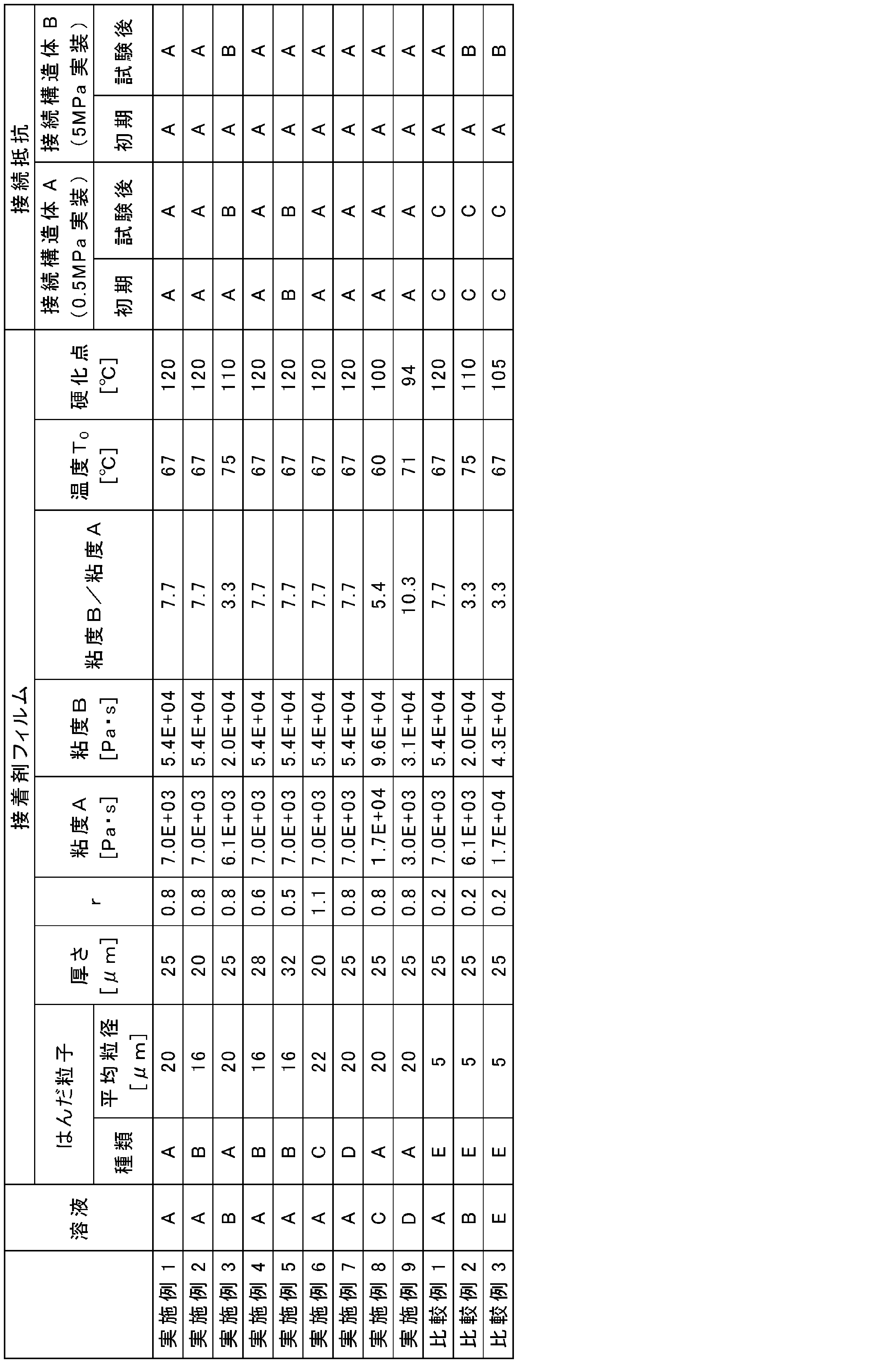
- the initial connection resistance and the connection resistance after the reliability test were evaluated according to the following criteria. Table 1 shows the results.
- X ( ⁇ ) be the average value of the connection resistance values (initial resistance values) measured at a plurality of electrodes in the connection structure immediately after production, and let X be 0.01 ⁇ or less as “A”, and X is A value of 0.05 ⁇ or less was rated as “B”, and a value of over 0.05 ⁇ was rated as "C”.
- Y ( ⁇ ) is the average value of connection resistance values measured at a plurality of electrodes in the connection structure after the reliability test, and the rate of increase from the initial resistance value calculated by the formula: Y/X is 2 or less. Those exceeding 2 and 5 or less were designated as "A”, those exceeding 5 were designated as "C”.
Landscapes
- Chemical & Material Sciences (AREA)
- Organic Chemistry (AREA)
- Engineering & Computer Science (AREA)
- Microelectronics & Electronic Packaging (AREA)
- Manufacturing & Machinery (AREA)
- Inorganic Chemistry (AREA)
- Adhesives Or Adhesive Processes (AREA)
- Electric Connection Of Electric Components To Printed Circuits (AREA)
Abstract
Description
一実施形態のフィルム状接着剤は、Bi含有量が20~60質量%であり且つSn含有量が40~80質量%であるはんだ粒子と、ラジカル重合性化合物と、熱ラジカル発生剤と、を含有し、はんだ粒子の平均粒径が、フィルム状接着剤の厚さの0.5~1.5倍である、回路接続用のフィルム状接着剤である。
(A)成分は、20~60質量%のBi(ビスマス)と、40~80質量%のSn(スズ)とを含有する。BiとSnの組成が上記範囲であると、熱圧着時、139℃付近で溶融した液体状態のはんだ成分と、固体状態のはんだ成分が混在することになり、電極の接続間距離を保ちながら電極表面にはんだ粒子がぬれ広がり、密接かつ広範囲な物理的接触と部分的な金属接合(はんだの金属元素と電極めっき最表面の金属元素とが混合された層)を形成することが可能である。このような金属接合を形成しやすい観点では、(A)成分は、Bi含有量が21~58質量%であり且つSn含有量が42~79質量%であるはんだ粒子であってもよく、Bi含有量が21~40質量%であり且つSn含有量が60~79質量%であるはんだ粒子であってもよい。
(B)成分は、ラジカル重合可能な官能基を有する化合物である。(B)成分としては、(メタ)アクリレート化合物、マレイミド化合物、シトラコンイミド化合物、ナジイミド化合物等が挙げられる。「(メタ)アクリレート化合物」とは、(メタ)アクリロイル基を有する化合物を意味する。(B)成分は、モノマー又はオリゴマーの状態で用いてもよく、モノマーとオリゴマーとを併用することもできる。(B)成分は、1種単独で用いてもよく、2種以上を組み合わせて用いてもよい。
(C)成分は、熱により分解して遊離ラジカルを発生する硬化剤(熱ラジカル重合開始剤等)である。(C)成分としては、過酸化物(有機過酸化物等)、アゾ系化合物などが挙げられる。(C)成分は、目的とする接続温度、接続時間、ポットライフ等により適宜選定される。
フィルム状接着剤1は、上記(A)成分、(B)成分及び(C)成分以外の成分(その他の成分)を更に含有してよい。その他の成分としては、例えば、(D)リン酸エステル系有機化合物(以下、「(D)成分」ともいう。)、(E)フィルム形成材(以下、「(E)成分」ともいう。)、(F)無機充填材(以下、「(F)成分」ともいう。)及び(G)シランカップリング剤(以下、「(G)成分」ともいう。)が挙げられる。
(D)成分は、はんだ粒子表面と電極の表面の活性を上げ、はんだ粒子界面と電極界面との部分的な金属接合、はんだ粒子との密接かつ広い接触界面を発現する効果の向上に寄与する。かかる効果が得られやすくなる観点から、(D)成分は、単官能又は多官能のリン酸エステル系ラジカル重合性化合物であってよい。特に、(D)成分として、下記一般式(I)又は(II)で表されるリン酸エステル構造を有するラジカル重合性化合物を用いる場合に上記効果がより得られやすくなり、(メタ)アクリレート化合物等のラジカル重合性化合物と、式(I)又は(II)で表されるリン酸エステル構造を有するラジカル重合性化合物とを併用する場合に上記効果が更に得られやすくなる。なお、本明細書において、(D)成分は、(B)成分に含まれない。


(E)成分は、液状の接着剤組成物をフィルム状に固形化した場合に、通常の状態(常温常圧)でのフィルムの取扱い性を向上させ、裂け難い、割れ難い、べたつき難い等の特性をフィルムに付与することができる。フィルム形成材としては、フェノキシ樹脂、ポリビニルホルマール樹脂、ポリスチレン樹脂、ポリビニルブチラール樹脂、ポリエステル樹脂、ポリアミド樹脂、キシレン樹脂、ポリウレタン樹脂等が挙げられる。これらの中でも、ポリエステルウレタン樹脂及びフェノキシ樹脂が好ましく用いられる。特に、フェノキシ樹脂を用いる場合、接着性、相溶性、耐熱性及び機械的強度に優れる傾向がある。フィルム形成材は、1種単独で用いてもよく、2種以上を組み合わせて用いてもよい。
(F)成分は、例えば、非導電性の無機粒子である。(F)成分としては、例えば、シリカ微粒子、アルミナ微粒子、シリカ-アルミナ微粒子、チタニア微粒子、ジルコニア微粒子等の金属酸化物微粒子;金属窒化物微粒子などの無機微粒子が挙げられる。これらは、1種を単独で用いてもよく、複数種を組み合わせて用いてもよい。
(G)成分は、フィルム状接着剤1の密着力(ガラスに対する密着力等)の向上に寄与する。(G)成分としては、例えば、ビニルトリメトキシシラン、ビニルトリエトキシシラン、3-グリシドキシプロピルトリメトキシシラン、3-グリシドキシプロピルメチルジエトキシシラン、3-(メタ)アクリロキシプロピルメチルジメトキシシラン、3-(メタ)アクリロキシプロピルトリメトキシシラン、3-(メタ)アクリロキシプロピルメチルジエトキシシラン、3-(メタ)アクリロキシプロピルトリエトキシシラン、N-2-(アミノエチル)-3-アミノプロピルメチルジメトキシシラン、N-フェニル-3-アミノプロピルトリメトキシシラン、3-ウレイドプロピルトリエトキシシラン、3-メルカプトプロピルトリメトキシシラン、3-イソシアネートプロピルトリエトキシシラン、及び、これらの縮合物が挙げられる。
フィルム状接着剤1は、その他の成分として、重合禁止剤、軟化剤、促進剤、老化防止剤、着色剤、難燃化剤、チキソトロピック剤、カップリング剤、密着性向上剤(カップリング剤を除く)、増粘剤、レベリング剤、着色剤、耐候性向上剤等のその他の添加剤を適宜含有してもよい。その他の添加剤を更に含んでいてもよい。その他の添加剤の含有量は、接着剤成分の合計量100質量部に対して、例えば、0.1~10質量部であってよい。
一実施形態の接続構造体の製造方法は、第一の電極を有する第一の回路部材の第一の電極が設けられている面と、第二の電極を有する第二の回路部材の第二の電極が設けられている面との間に、フィルム状接着剤を配置する工程と、第一の回路部材と第二の回路部材とを、フィルム状接着剤を介して、1MPa以下の圧力で熱圧着することにより、第一の電極と第二の電極とを互いに電気的に接続し且つ第一の回路部材と第二の回路部材とを接着する工程と、を含む。フィルム状接着剤は、例えば、上記実施形態のフィルム状接着剤である。
ラジカル重合性化合物である、ウレタンアクリレート(製品名:UN-952、根上工業株式会社製)5質量部及びイソシアヌル酸EO変性ジアクリレート(製品名:M-215、東亞合成株式会社製)10質量部と、リン酸エステル系有機化合物である、2-ヒドロキシエチルメタクリレートの6-ヘキサノリド付加重合物と無水リン酸との反応生成物(製品名:PM-21、日本化薬株式会社製)2質量部と、熱ラジカル発生剤である、パーオキシエステル(製品名:パーヘキサ25O、日油株式会社製)3質量部と、無機充填材である、シリカフィラー(製品名:AEROSIL R202、日本アエロジル株式会社)15質量部と、フィルム形成材であるポリエステルウレタン樹脂(製品名:UR8240、東洋紡株式会社製)35質量部と、をメチルエチルケトン中で混合し、攪拌して、溶液Aを得た。
三井金属鉱業株式会社製のはんだ粒子(商品名:Sn72Bi28 DS10)に対して分級操作を行い、粒子径が12μm以下のはんだ粒子及び粒子径が20μm以上のはんだ粒子を除去することで、はんだ粒子B(Bi含有量:28質量%、Sn含有量:72質量%、平均粒径:16μm、軟化点:139℃)を得た。はんだ粒子Bの平均粒径は、はんだ粒子BのD50値をマイクロトラック測定装置で測定して確認した。はんだ粒子Aに代えてはんだ粒子Bを用いたこと、及び、乾燥後に得られるフィルム状接着剤の厚さが20μmとなるように塗工条件を変更したことを除き、実施例1と同様にして、PETフィルム上に異方導電性のフィルム状接着剤(厚さ:20μm)を形成した。これにより、実施例2の剥離性基材付きフィルム状接着剤(フィルム状接着剤の厚さに対するはんだ粒子の平均粒径の比r=0.8)を得た。なお、フィルム状接着剤の厚さは実施例1と同様にして測定した。
フェノキシ樹脂(商品名:PKHC、ユニオンカーバイド株式会社製)50gを、トルエン/酢酸エチル(質量比:50/50)の混合溶剤に溶解して、固形分40%のフェノキシ樹脂溶液を用意した。このフェノキシ樹脂溶液を35質量部(フェノキシ樹脂14質量部)と、ラジカル重合性化合物である、イソシアヌル酸EO(エチレンオキサイド)変性ジアクリレート(商品名:M-215、東亜合成株式会社製)14質量部及びウレタンアクリレート(商品名:U-2PPA、新中村化学株式会社製)14質量部と、リン酸エステル系有機化合物である、2-メタクリロイルオキシエチルアシッドフォスフェート(商品名:ライトエステルP-2M、共栄社化学株式会社製)3質量部と、シランカップリング剤である、3-メタクリロキシプロピルトリメトキシシラン(商品名:KBM-503、信越化学工業株式会社製)2質量部と、熱ラジカル発生剤である、パーオキシエステル(商品名:パーヘキサ25O、日油株式会社製)2質量部と、を混合し、溶液Bを得た。
乾燥後の厚さが28μmとなるように塗工条件を変更したことを除き、実施例2と同様にして、PETフィルム上に異方導電性のフィルム状接着剤(厚さ:28μm)を形成した。これにより、実施例4の剥離性基材付きフィルム状接着剤(フィルム状接着剤の厚さに対するはんだ粒子の平均粒径の比r=0.6)を得た。なお、フィルム状接着剤の厚さは実施例1と同様にして測定した。
乾燥後の厚さが32μmとなるように塗工条件を変更したことを除き、実施例2と同様にして、PETフィルム上に異方導電性のフィルム状接着剤(厚さ:32μm)を形成した。これにより、実施例5の剥離性基材付きフィルム状接着剤(フィルム状接着剤の厚さに対するはんだ粒子の平均粒径の比r=0.5)を得た。なお、フィルム状接着剤の厚さは実施例1と同様にして測定した。
三井金属鉱業株式会社製のはんだ粒子(商品名:Sn72Bi28 Type5)に対して分級操作を行い、粒子径が20μm以下のはんだ粒子及び粒子径が25μm以上のはんだ粒子を除去することで、はんだ粒子C(Bi含有量:28質量%、Sn含有量:72質量%、平均粒径:22μm、軟化点:139℃)を得た。はんだ粒子Cの平均粒径は、はんだ粒子CのD50値をマイクロトラック測定装置で測定して確認した。得られたはんだ粒子Cとメチルエチルケトンとを、実施例1で調製した溶液Aに加えて分散させ、塗工液を得た。この際、はんだ粒子Cの添加量は、溶液A中の不揮発分(メチルエチルケトン以外の成分)100質量部に対し、30質量部とし、メチルエチルケトンの添加量は20質量部とした。
三井金属鉱業株式会社製のはんだ粒子(商品名:Sn42Bi58 Type5)に対して分級操作を行い、粒子径が15μm以下のはんだ粒子及び粒子径が25μm以上のはんだ粒子を除去することで、はんだ粒子D(Bi含有量:58質量%、Sn含有量:42質量%、平均粒径:20μm、軟化点:139℃)を得た。はんだ粒子Dの平均粒径は、はんだ粒子DのD50値をマイクロトラック測定装置で測定して確認した。はんだ粒子Aに代えて上記で得られたはんだ粒子Dを用いたことを除き、実施例1と同様にして、PETフィルム上に異方導電性のフィルム状接着剤(厚さ:25μm)を形成した。これにより、実施例7の剥離性基材付きフィルム状接着剤(フィルム状接着剤の厚さに対するはんだ粒子の平均粒径の比r=0.8)を得た。なお、フィルム状接着剤の厚さは実施例1と同様にして測定した。
ラジカル重合性化合物である、カーボネート系ウレタンアクリレート(製品名:UN-5500、根上工業株式会社製)10質量部、イソシアヌル酸EO変性ジアクリレート(製品名:M-215、東亞合成株式会社製)5質量部及びジメチロールトリシクロデカンジアクリレート(製品名:DCP-A、共栄社化学株式会社製)5質量部と、リン酸エステル系有機化合物である、2-メタクリロイロキシエチルアッシドフォスヘート(製品名:ライトエステルP-2M、共栄社化学株式会社製)1質量部と、ウレタンフィラー(製品名:MM-101SM、根上工業株式会社)10質量部と、熱ラジカル発生剤(遊離ラジカル発生剤)であるジアシルパーオキサイド(製品名:パーロイルL、日油株式会社製)8質量部と、絶縁性樹脂であるポリエステルウレタン樹脂(製品名:UR4800、東洋紡株式会社製)31質量部を含むメチルエチルケトン溶液と、を混合し、攪拌して、溶液Cを得た。
フェノキシ樹脂(商品名:PKHC、ユニオンカーバイド株式会社製)を、トルエン/酢酸エチル(質量比:50/50)の混合溶剤に溶解して、固形分40%のフェノキシ樹脂溶液を用意した。このフェノキシ樹脂溶液を10質量部(フェノキシ樹脂4質量部)と、ラジカル重合性化合物である、ウレタンアクリレート(製品名:UN-952、根上工業株式会社製)10質量部及びイソシアヌル酸EO変性ジアクリレート(製品名:M-215、東亞合成株式会社製)10質量部と、リン酸エステル系有機化合物である、2-ヒドロキシエチルメタクリレートの6-ヘキサノリド付加重合物と無水リン酸との反応生成物(製品名:PM-21、日本化薬株式会社製)2質量部と、重重合禁止剤(製品名:LA-7RD、株式会社ADEKA)0.1質量部と、熱ラジカル発生剤である、パーオキシエステル(製品名:パーヘキサ25O、日油株式会社製)3質量部と、有機微粒子(製品名:EXL―2655、ローム・アンド・ハース・ジャパン株式会社)15質量部と、フィルム形成材であるポリエステルウレタン樹脂(製品名:UR4800、東洋紡株式会社製)20質量部と、をメチルエチルケトン中で混合し、攪拌して、溶液Dを得た。
はんだ粒子Eとして、三井金属鉱業株式会社製のはんだ粒子(Bi含有量:28質量%、Sn含有量:72質量%、平均粒径:5μm、軟化点:139℃、商品名:ST-5)を用意した。はんだ粒子Eの平均粒径は、はんだ粒子EのD50値をマイクロトラック測定装置で測定して確認した。はんだ粒子Aに代えてはんだ粒子Eを用いたことを除き、実施例1と同様にして、PETフィルム上に異方導電性のフィルム状接着剤(厚さ25μm)を形成した。これにより、比較例1の剥離性基材付きフィルム状接着剤(フィルム状接着剤の厚さに対するはんだ粒子の平均粒径の比r=0.2)を得た。なお、フィルム状接着剤の厚さは実施例1と同様にして測定した。
溶液Aに代えて溶液Bを用いたことを除き、比較例1と同様にして、PETフィルム上に異方導電性のフィルム状接着剤(厚さ:25μm)を形成した。これにより、比較例2の剥離性基材付きフィルム状接着剤(フィルム状接着剤の厚さに対するはんだ粒子の平均粒径の比r=0.2)を得た。なお、フィルム状接着剤の厚さは実施例1と同様にして測定した。
ラジカル重合性化合物である、カーボネート系ウレタンアクリレート(製品名:UN-5500、根上工業株式会社製)13質量部、トリス(アクリロキシエチル)イソシアヌレート(製品名:M-315、東亞合成株式会社製)10質量部及びジメチロールトリシクロデカンジアクリレート(製品名:DCP-A、共栄社化学株式会社製)5質量部と、リン酸エステル系有機化合物である、2-2-メタクリロイルオキシエチルアシッドフォスフェート(製品名:ライトエステルP-2M、共栄社化学株式会社製)1質量部と、熱ラジカル発生剤である、ベンゾイルパーオキサイド(製品名:ナイパーBMT-K、日油株式会社製)5質量部と、フィルム形成材である、ポリエステルウレタン樹脂(製品名:UR4800、東洋紡株式会社製)33質量部と、をメチルエチルケトン中で混合し、メチルエチルケトン溶液を得た。その後、得られたメチルエチルケトン溶液に、ポリスチレン微粒子(商品名:PB-3006W、松浦株式会社製、平均粒径:6μm)3質量部を混合し、溶液Eを得た。
(フィルム状接着剤の粘度測定)
以下の方法で、実施例1~9及び比較例1~3のフィルム状接着剤の硬化点、最低溶融粘度(粘度A)及びはんだ粒子の軟化点(139℃)における粘度(粘度B)を測定した。
回路部材を模した被着体として、セラミック基板の表面に金電極(10mm×5mm、単一電極)が設けられた第一の部材を準備した。次いで、上記で得られた剥離性基材付きフィルム状接着剤を1.5mm幅にカットし、フィルム状接着剤側から、第一の部材の金電極上に貼り付けた。次いで、PETフィルム側から熱圧着装置(加熱方式:コンスタントヒート型、日化設備エンジニアリング株式会社製)を用いて、フィルム状接着剤の到達温度が70℃となるように加熱しながら加圧(熱圧着)した。圧着時間は1秒間とし、加圧の圧力は、フィルム状接着剤の総面積(接着部分の面積)あたりで1MPaとした。得られた圧着体が常温に戻った後、圧着体からPETフィルムを剥離し、第一の部材上にフィルム状接着剤が設けられてなる積層体を得た。
[初期の接続抵抗]
製造直後の接続構造体における複数の電極で測定された接続抵抗値(初期抵抗値)の平均値をX(Ω)とし、Xが0.01Ω以下であったものを「A」とし、Xが0.05Ω以下であったものを「B」とし、0.05Ωを超えたものを「C」とした。
[信頼性試験後の接続抵抗]
信頼性試験後の接続構造体における複数の電極で測定された接続抵抗値の平均値をY(Ω)とし、式:Y/Xで算出される初期抵抗値からの上昇率が2以下であったものを「A」とし、2を超え5以下であったものを「B」とし、5を超えたものを「C」とした。
Claims (6)
- 回路接続用のフィルム状接着剤であって、
Bi含有量が20~60質量%であり且つSn含有量が40~80質量%であるはんだ粒子と、ラジカル重合性化合物と、熱ラジカル発生剤と、を含有し、
前記はんだ粒子の平均粒径が、前記フィルム状接着剤の厚さの0.5~1.5倍である、フィルム状接着剤。 - 前記はんだ粒子の軟化点よりも低い温度に硬化点を有する、請求項1に記載のフィルム状接着剤。
- 前記はんだ粒子の軟化点での前記フィルム状接着剤の粘度が、最低溶融粘度の3倍以上である、請求項1又は2に記載のフィルム状接着剤。
- 前記はんだ粒子の軟化点が130~180℃である、請求項1~3のいずれか一項に記載のフィルム状接着剤。
- 第一の電極を有する第一の回路部材の前記第一の電極が設けられている面と、第二の電極を有する第二の回路部材の前記第二の電極が設けられている面との間に、請求項1~4のいずれか一項に記載のフィルム状接着剤を配置する工程と、
前記第一の回路部材と前記第二の回路部材とを、前記フィルム状接着剤を介して、1MPa以下の圧力で熱圧着することにより、前記第一の電極と前記第二の電極とを互いに電気的に接続し且つ前記第一の回路部材と前記第二の回路部材とを接着する工程と、を含む、接続構造体の製造方法。 - 前記第一の電極が、最表面にAuめっき層を有する電極であり、
前記第二の電極が、最表面にAuめっき層又はSnめっき層を有する電極である、請求項5に記載の接続構造体の製造方法。
Priority Applications (3)
| Application Number | Priority Date | Filing Date | Title |
|---|---|---|---|
| KR1020237027712A KR20230135612A (ko) | 2021-01-25 | 2022-01-24 | 필름상 접착제 및 접속 구조체의 제조 방법 |
| CN202280011098.3A CN116802243A (zh) | 2021-01-25 | 2022-01-24 | 膜状黏合剂及连接结构体的制造方法 |
| JP2022576772A JP7729354B2 (ja) | 2021-01-25 | 2022-01-24 | フィルム状接着剤及び接続構造体の製造方法 |
Applications Claiming Priority (2)
| Application Number | Priority Date | Filing Date | Title |
|---|---|---|---|
| JP2021009738 | 2021-01-25 | ||
| JP2021-009738 | 2021-01-25 |
Publications (1)
| Publication Number | Publication Date |
|---|---|
| WO2022158594A1 true WO2022158594A1 (ja) | 2022-07-28 |
Family
ID=82548763
Family Applications (1)
| Application Number | Title | Priority Date | Filing Date |
|---|---|---|---|
| PCT/JP2022/002460 Ceased WO2022158594A1 (ja) | 2021-01-25 | 2022-01-24 | フィルム状接着剤及び接続構造体の製造方法 |
Country Status (5)
| Country | Link |
|---|---|
| JP (1) | JP7729354B2 (ja) |
| KR (1) | KR20230135612A (ja) |
| CN (1) | CN116802243A (ja) |
| TW (1) | TWI885239B (ja) |
| WO (1) | WO2022158594A1 (ja) |
Cited By (1)
| Publication number | Priority date | Publication date | Assignee | Title |
|---|---|---|---|---|
| WO2025134747A1 (ja) * | 2023-12-22 | 2025-06-26 | 株式会社レゾナック | 回路接続用接着剤フィルム、接続構造体の製造方法、導電材料、及び接続構造体 |
Citations (7)
| Publication number | Priority date | Publication date | Assignee | Title |
|---|---|---|---|---|
| JP2000133681A (ja) * | 1998-10-23 | 2000-05-12 | Hitachi Chem Co Ltd | 回路部材の実装方法及び回路部材接続用接着剤 |
| JP2012079880A (ja) * | 2010-09-30 | 2012-04-19 | Sumitomo Bakelite Co Ltd | 接着剤、多層回路基板、半導体用部品および半導体装置 |
| WO2017090659A1 (ja) * | 2015-11-25 | 2017-06-01 | 日立化成株式会社 | 回路接続用接着剤組成物及び構造体 |
| JP2017120839A (ja) * | 2015-12-28 | 2017-07-06 | 千住金属工業株式会社 | 導電接合シートおよび導電接合シートの製造方法。 |
| WO2017170371A1 (ja) * | 2016-03-30 | 2017-10-05 | 積水化学工業株式会社 | 導電性粘着テープ |
| JP2019044043A (ja) * | 2017-08-31 | 2019-03-22 | 日立化成株式会社 | 回路接続用接着剤組成物及び構造体 |
| JP2020024937A (ja) * | 2019-10-28 | 2020-02-13 | 日立化成株式会社 | フィルム状回路接続材料及び回路部材の接続構造体の製造方法 |
Family Cites Families (3)
| Publication number | Priority date | Publication date | Assignee | Title |
|---|---|---|---|---|
| JPS60191228A (ja) | 1984-10-29 | 1985-09-28 | Seiko Epson Corp | 表示装置の接続構造 |
| JPH01251787A (ja) | 1988-03-31 | 1989-10-06 | Toshiba Corp | 電子部品の接続装置 |
| JPWO2009063827A1 (ja) | 2007-11-12 | 2011-03-31 | 日立化成工業株式会社 | 回路接続材料、及び回路部材の接続構造 |
-
2022
- 2022-01-24 TW TW111102989A patent/TWI885239B/zh active
- 2022-01-24 JP JP2022576772A patent/JP7729354B2/ja active Active
- 2022-01-24 WO PCT/JP2022/002460 patent/WO2022158594A1/ja not_active Ceased
- 2022-01-24 CN CN202280011098.3A patent/CN116802243A/zh active Pending
- 2022-01-24 KR KR1020237027712A patent/KR20230135612A/ko active Pending
Patent Citations (7)
| Publication number | Priority date | Publication date | Assignee | Title |
|---|---|---|---|---|
| JP2000133681A (ja) * | 1998-10-23 | 2000-05-12 | Hitachi Chem Co Ltd | 回路部材の実装方法及び回路部材接続用接着剤 |
| JP2012079880A (ja) * | 2010-09-30 | 2012-04-19 | Sumitomo Bakelite Co Ltd | 接着剤、多層回路基板、半導体用部品および半導体装置 |
| WO2017090659A1 (ja) * | 2015-11-25 | 2017-06-01 | 日立化成株式会社 | 回路接続用接着剤組成物及び構造体 |
| JP2017120839A (ja) * | 2015-12-28 | 2017-07-06 | 千住金属工業株式会社 | 導電接合シートおよび導電接合シートの製造方法。 |
| WO2017170371A1 (ja) * | 2016-03-30 | 2017-10-05 | 積水化学工業株式会社 | 導電性粘着テープ |
| JP2019044043A (ja) * | 2017-08-31 | 2019-03-22 | 日立化成株式会社 | 回路接続用接着剤組成物及び構造体 |
| JP2020024937A (ja) * | 2019-10-28 | 2020-02-13 | 日立化成株式会社 | フィルム状回路接続材料及び回路部材の接続構造体の製造方法 |
Cited By (1)
| Publication number | Priority date | Publication date | Assignee | Title |
|---|---|---|---|---|
| WO2025134747A1 (ja) * | 2023-12-22 | 2025-06-26 | 株式会社レゾナック | 回路接続用接着剤フィルム、接続構造体の製造方法、導電材料、及び接続構造体 |
Also Published As
| Publication number | Publication date |
|---|---|
| KR20230135612A (ko) | 2023-09-25 |
| CN116802243A (zh) | 2023-09-22 |
| TW202239920A (zh) | 2022-10-16 |
| TWI885239B (zh) | 2025-06-01 |
| JP7729354B2 (ja) | 2025-08-26 |
| JPWO2022158594A1 (ja) | 2022-07-28 |
Similar Documents
| Publication | Publication Date | Title |
|---|---|---|
| US9023464B2 (en) | Connecting film, and joined structure and method for producing the same | |
| JP5067355B2 (ja) | 回路接続材料及び回路部材の接続構造 | |
| JP5867508B2 (ja) | 回路接続材料及び接続体 | |
| JPWO2009078409A1 (ja) | 回路接続材料及び回路部材の接続構造 | |
| KR20210134875A (ko) | 접착제 조성물 및 접속체 | |
| JP7006029B2 (ja) | 回路接続用接着剤組成物及び構造体 | |
| JP6870618B2 (ja) | 回路接続用接着剤組成物及び構造体 | |
| JP2022000530A (ja) | 接着剤組成物及び構造体 | |
| KR102905241B1 (ko) | 접속 구조체, 회로 접속 부재 및 접착제 조성물 | |
| JP4752107B2 (ja) | 回路接続用フィルム状接着剤、回路端子の接続構造および回路端子の接続方法 | |
| JP7729354B2 (ja) | フィルム状接着剤及び接続構造体の製造方法 | |
| JP2007224228A (ja) | 回路接続材料並びに回路端子の接続構造体及び接続方法 | |
| JP4945881B2 (ja) | 回路接続用支持体付接着剤、及びそれを用いた回路接続構造体 | |
| JP7755481B2 (ja) | 接着剤組成物、異方性導電フィルム、接続構造体および接続構造体の製造方法 | |
| WO2022186016A1 (ja) | 回路接続用接着フィルム及び接続体 | |
| JP5365666B2 (ja) | 回路接続材料並びに回路端子の接続構造体及び接続方法 | |
| JP2010212706A (ja) | 回路接続材料及びそれを用いた回路板の製造方法、回路板 | |
| JP2025029739A (ja) | 接着剤組成物、回路接続用接着剤フィルム、回路接続構造体及びその製造方法 | |
| TW201410823A (zh) | 接著劑組成物及連接體 | |
| KR20080103462A (ko) | 접착제 조성물 |
Legal Events
| Date | Code | Title | Description |
|---|---|---|---|
| 121 | Ep: the epo has been informed by wipo that ep was designated in this application |
Ref document number: 22742713 Country of ref document: EP Kind code of ref document: A1 |
|
| ENP | Entry into the national phase |
Ref document number: 2022576772 Country of ref document: JP Kind code of ref document: A |
|
| WWE | Wipo information: entry into national phase |
Ref document number: 202280011098.3 Country of ref document: CN |
|
| ENP | Entry into the national phase |
Ref document number: 20237027712 Country of ref document: KR Kind code of ref document: A |
|
| WWE | Wipo information: entry into national phase |
Ref document number: 1020237027712 Country of ref document: KR |
|
| NENP | Non-entry into the national phase |
Ref country code: DE |
|
| 122 | Ep: pct application non-entry in european phase |
Ref document number: 22742713 Country of ref document: EP Kind code of ref document: A1 |