WO2022158349A1 - 半導体記憶装置 - Google Patents
半導体記憶装置 Download PDFInfo
- Publication number
- WO2022158349A1 WO2022158349A1 PCT/JP2022/000708 JP2022000708W WO2022158349A1 WO 2022158349 A1 WO2022158349 A1 WO 2022158349A1 JP 2022000708 W JP2022000708 W JP 2022000708W WO 2022158349 A1 WO2022158349 A1 WO 2022158349A1
- Authority
- WO
- WIPO (PCT)
- Prior art keywords
- data
- value
- bit
- defect information
- bits
- Prior art date
- Legal status (The legal status is an assumption and is not a legal conclusion. Google has not performed a legal analysis and makes no representation as to the accuracy of the status listed.)
- Ceased
Links
Images




Classifications
-
- G—PHYSICS
- G11—INFORMATION STORAGE
- G11C—STATIC STORES
- G11C29/00—Checking stores for correct operation ; Subsequent repair; Testing stores during standby or offline operation
- G11C29/56—External testing equipment for static stores, e.g. automatic test equipment [ATE]; Interfaces therefor
- G11C29/56016—Apparatus features
-
- G—PHYSICS
- G01—MEASURING; TESTING
- G01R—MEASURING ELECTRIC VARIABLES; MEASURING MAGNETIC VARIABLES
- G01R31/00—Arrangements for testing electric properties; Arrangements for locating electric faults; Arrangements for electrical testing characterised by what is being tested not provided for elsewhere
- G01R31/28—Testing of electronic circuits, e.g. by signal tracer
-
- G—PHYSICS
- G11—INFORMATION STORAGE
- G11C—STATIC STORES
- G11C29/00—Checking stores for correct operation ; Subsequent repair; Testing stores during standby or offline operation
- G11C29/04—Detection or location of defective memory elements, e.g. cell constructio details, timing of test signals
- G11C29/08—Functional testing, e.g. testing during refresh, power-on self testing [POST] or distributed testing
- G11C29/12—Built-in arrangements for testing, e.g. built-in self testing [BIST] or interconnection details
- G11C29/38—Response verification devices
- G11C29/42—Response verification devices using error correcting codes [ECC] or parity check
-
- G—PHYSICS
- G11—INFORMATION STORAGE
- G11C—STATIC STORES
- G11C29/00—Checking stores for correct operation ; Subsequent repair; Testing stores during standby or offline operation
- G11C29/04—Detection or location of defective memory elements, e.g. cell constructio details, timing of test signals
- G11C29/08—Functional testing, e.g. testing during refresh, power-on self testing [POST] or distributed testing
- G11C29/12—Built-in arrangements for testing, e.g. built-in self testing [BIST] or interconnection details
- G11C29/44—Indication or identification of errors, e.g. for repair
-
- G—PHYSICS
- G11—INFORMATION STORAGE
- G11C—STATIC STORES
- G11C29/00—Checking stores for correct operation ; Subsequent repair; Testing stores during standby or offline operation
- G11C29/56—External testing equipment for static stores, e.g. automatic test equipment [ATE]; Interfaces therefor
- G11C29/56008—Error analysis, representation of errors
-
- H—ELECTRICITY
- H10—SEMICONDUCTOR DEVICES; ELECTRIC SOLID-STATE DEVICES NOT OTHERWISE PROVIDED FOR
- H10D—INORGANIC ELECTRIC SEMICONDUCTOR DEVICES
- H10D84/00—Integrated devices formed in or on semiconductor substrates that comprise only semiconducting layers, e.g. on Si wafers or on GaAs-on-Si wafers
-
- H—ELECTRICITY
- H10—SEMICONDUCTOR DEVICES; ELECTRIC SOLID-STATE DEVICES NOT OTHERWISE PROVIDED FOR
- H10D—INORGANIC ELECTRIC SEMICONDUCTOR DEVICES
- H10D84/00—Integrated devices formed in or on semiconductor substrates that comprise only semiconducting layers, e.g. on Si wafers or on GaAs-on-Si wafers
- H10D84/01—Manufacture or treatment
- H10D84/02—Manufacture or treatment characterised by using material-based technologies
- H10D84/03—Manufacture or treatment characterised by using material-based technologies using Group IV technology, e.g. silicon technology or silicon-carbide [SiC] technology
- H10D84/038—Manufacture or treatment characterised by using material-based technologies using Group IV technology, e.g. silicon technology or silicon-carbide [SiC] technology using silicon technology, e.g. SiGe
-
- G—PHYSICS
- G11—INFORMATION STORAGE
- G11C—STATIC STORES
- G11C29/00—Checking stores for correct operation ; Subsequent repair; Testing stores during standby or offline operation
- G11C29/56—External testing equipment for static stores, e.g. automatic test equipment [ATE]; Interfaces therefor
- G11C2029/5602—Interface to device under test
Definitions
- the memory 10 outputs defect information as n bits, which is smaller than the data width (m bits) for reading and writing data, and as a different value for each defect number. Therefore, it is possible to detect the number of defects up to the number that can be represented by n bits, and it is possible to test a memory that does not require pass determination of all bits.
- the XOR circuit 221 outputs the value [1] if the expected value [x] and the data [x] are different and the output of the XOR circuit 221 in the preceding unit 210 x-1 is the value [0]. to output (4) The XOR circuit 221 outputs the value [0] if the expected value [x] and the data [x] are different and the output of the XOR circuit 221 in the preceding unit 210 x-1 is the value [1]. to output
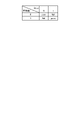
- Symbols a to f in the drawing indicate states corresponding to combinations of data (Data) [0] to [4] input to the five units 210.
- FIG. Code a indicates that all of data [0] to [4] have a value [0] (Low), that is, a pass state.
- Symbols b to f respectively indicate states in which 1 to 4 of data [1] to [4] are value [1], that is, fail.
- the defect number counter 200 counts the number of defects when the value (data [0] to [4]) read from each memory cell is different from the expected value [0]. [0]) and the first bit (bit [1]) in binary. It can be seen that the overflow information [overflow] has a value of [1] when the number of fail is four or more, which is the threshold value. That is, when the overflow information [overflow] is the 2nd bit for the 0th and 1st bits, the count result is fixed to the threshold value [4] when there are 4 or more fails.
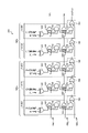
- FIG. 9 is a schematic diagram for explaining a first example of the first modification of the embodiment.
- each bit of IO is grouped into two groups, a group 260a of data [0] to [2] and a group 260b of data [3] and [4].
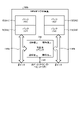
- FIG. 10 is a schematic diagram for explaining a second example of the first modified example of the embodiment.
- MRAM 100b (macro structure) includes four banks 150 (A1), 150 (A2), 150 (A3) and 150 (A4) as logical structural units of storage regions. These banks 150(A1), 150(A2), 150(A3) and 150(A4) can be considered as grouping the cell array 110 based on the logical configuration.
- each of these banks 150 (A1), 150 (A2), 150 (A3) and 150 (A4) is treated as a group, and expected values are set according to the group.
- the defect number counter 200 by setting the expected value according to the group in which each bit of the IO is grouped, A more detailed test becomes possible.
- the technology according to the embodiment can also be applied to semiconductor memory devices having other configurations.
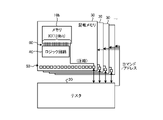
- the technology according to the embodiment can be applied to the embedded memory 30 described using FIG. 2B.
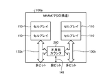
- the memory 10b mounted on the embedded memory 30 is provided with the defective number counter 200 described in the embodiment.
- the adder is Constituted by repetition of a pattern for each bit of data read from the memory cell array, The semiconductor memory device according to (5) above.
- the defect information acquisition unit a comparator that compares data read from the memory cell array with a preset expected value for the read data; activating a signal indicating that the read data is defective when the comparison result by the comparator indicates that the read data is different from the expected value;
- the semiconductor memory device according to any one of (1) to (6).
- the defect information acquisition unit The expected value is set according to each of a plurality of groups obtained by grouping data read simultaneously from the memory cell array.
- the defect information acquisition unit The expected value is set according to each of a plurality of groups obtained by grouping the memory cell array based on a logical configuration.
- the defect information acquisition unit The output terminal for outputting the defect information is shared with the output terminal for the read data output unit to output data;
- (11) further comprising a logic circuit connected to the read data output unit;
- the memory cell A resistance variable element is used as a memory element for storing data, The semiconductor memory device according to any one of (1) to (11) above.
- the memory cell A magnetoresistive element is used as a memory element for storing data, The semiconductor memory device according to any one of (1) to (12) above.
Landscapes
- Engineering & Computer Science (AREA)
- General Engineering & Computer Science (AREA)
- Physics & Mathematics (AREA)
- General Physics & Mathematics (AREA)
- For Increasing The Reliability Of Semiconductor Memories (AREA)
- Tests Of Electronic Circuits (AREA)
- Semiconductor Integrated Circuits (AREA)
Abstract
Description
1.本開示の概略
2.既存技術について
3.本開示の実施形態について
4.実施形態の第1の変形例
4-1.実施形態の第1の変形例の第1の例
4-2.実施形態の第1の変形例の第2の例
5.実施形態の第2の変形例
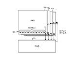
先ず、本開示の技術について、概略的に説明する。図1は、本開示の技術を適用可能なメモリの検査システムを概略的に示す模式図である。
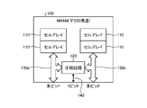
次に、本開示の実施形態の説明に先んじて、理解を容易とするために、既存技術について説明する。
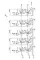
次に、本開示の実施形態について説明する。図4は、実施形態に係る半導体記憶装置としてのMRAM(マクロ構造)の一例の構成を示すブロック図である。図4に示される、実施形態に係るMRAM100aは、図3に示した既存技術によるMRAM100の構成に対して、圧縮回路120の代わりに不良数カウンタ200が設けられる。なお、図4において、テスタ20からコマンドおよびアドレスを指示される信号線および端子は、省略されている。
(1)XOR回路221は、期待値[x]とデータ[x]とが一致し、且つ、前段のユニット210x-1におけるXOR回路221の出力(ユニット2101においては端子2501)が値[0]であれば、値[0]を出力する。
(2)XOR回路221は、期待値[x]とデータ[x]とが一致し、且つ、前段のユニット210x-1におけるXOR回路221(ユニット2101以外の場合)の出力が値[1]であれば、値[1]を出力する。
(3)XOR回路221は、期待値[x]とデータ[x]とが異なり、且つ、前段のユニット210x-1におけるXOR回路221の出力が値[0]であれば、値[1]を出力する。
(4)XOR回路221は、期待値[x]とデータ[x]とが異なり、且つ、前段のユニット210x-1におけるXOR回路221の出力が値[1]であれば、値[0]を出力する。
(1)AND回路230は、期待値[x]とデータ[x]とが一致し、且つ、前段のユニット210x-1におけるXOR回路221の出力(ユニット2101においては端子2501)が値[0]であれば、値[0]を出力する。
(2)AND回路230は、期待値[x]とデータ[x]とが一致し、且つ、前段のユニット210x-1におけるXOR回路221(ユニット2101以外の場合)の出力が値[1]であれば、値[0]を出力する。
(3)AND回路230は、期待値[x]とデータ[x]とが異なり、且つ、前段のユニット210x-1におけるXOR回路221の出力が値[0]であれば、値[0]を出力する。
(4)AND回路230は、期待値[x]とデータ[x]とが異なり、且つ、前段のユニット210x-1におけるXOR回路221の出力が値[1]であれば、値[1]を出力する。
次に、本開示の実施形態の第1の変形例について説明する。実施形態の第1の変形例は、メモリのIOをグルーピングし、不良数カウンタ200において、グルーピングされたグループに応じて期待値を設定する例である。
先ず、4-1.実施形態の第1の変形例の第1の例について説明する。図9は、実施形態の第1の変形例の第1の例を説明するための模式図である。図9において、不良数カウンタ200は、値m=5、値n=2、オーバーフローに対する閾値を[4]とした場合の構成例を示している。
次に、実施形態の第1の変形例の第2の例について説明する。上述した実施形態の第1の変形例の第1の例では、IOの各ビットを、ハードウェア構成に基づいてグルーピングしていた。これに対して、実施形態の第1の変形例の第2の例では、IOの各ビットを、メモリの論理構成に基づいてグルーピングし、グループに応じて期待値を設定する。
次に、実施形態の第2の変形例について説明する。上述の実施形態では、MRAM100aにおいて、メモリのIOの端子と、不良数カウンタ200がテスト結果データを出力するための端子とを別個に設けていた。これに対して、実施形態の第2の変形例では、メモリのIOの端子と、テスト結果データを出力するための端子とを共有する。
(1)
複数のメモリセルを含むメモリセルアレイと、
前記メモリセルアレイから読み出されたデータを変更せずに、mビットのビット幅で外部に出力する読出データ出力部と、
前記メモリセルアレイから読み出したデータに不良が検出された場合に前記不良を示す不良情報を取得する不良情報取得部と、
を備え、
前記不良情報取得部は、
前記メモリセルアレイから読み出されたデータの不良数が0乃至nビット(n<m)ビットで不良数毎に異なる値を外部へ出力するための、それぞれ1ビットの情報を表す2つ以上且つn個以下のビット値により不良情報を出力する、
半導体記憶装置。
(2)
前記不良情報取得部は、
前記不良数を表すビット値のうちLSB(Least Significant Bit)から前記nビットまでのビット数のビット値を取得する、
前記(1)に記載の半導体記憶装置。
(3)
前記不良情報取得部は、
前記不良数が前記nビットで表現できる数を超えた場合に、判別信号を出力する、
前記(2)に記載の半導体記憶装置。
(4)
前記不良情報取得部は、
前記不良情報のうち最上位ビットの値がインクリメントされた状態で、前記不良がさらに検出された場合に、前記最上位ビットの値を反転しない、
前記(1)乃至(3)の何れかに記載の半導体記憶装置。
(5)
前記不良情報取得部は、
前記メモリセルアレイから同時に読み出されたデータに含まれる不良をカウントする加算器を含む、
前記(1)乃至(4)の何れかに記載の半導体記憶装置。
(6)
前記加算器は、
前記メモリセルアレイから読み出されるデータのビット毎のパターンの繰り返により構成される、
前記(5)に記載の半導体記憶装置。
(7)
前記不良情報取得部は、
前記メモリセルアレイから読み出されたデータと、前記読み出されたデータに対して予め設定された期待値と、を比較する比較器を含み、
前記比較器による比較結果が、前記読み出されたデータと前記期待値とが異なることを示している場合に、前記読み出されたデータが不良である旨を示す信号を活性化する、
前記(1)乃至(6)の何れかに記載の半導体記憶装置。
(8)
前記不良情報取得部は、
前記メモリセルアレイから同時に読み出されるデータをグルーピングした複数のグループそれぞれに応じて、前記期待値が設定される、
前記(7)に記載の半導体記憶装置。
(9)
前記不良情報取得部は、
前記メモリセルアレイを論理構成に基づきグルーピングした複数のグループそれぞれに応じて、前記期待値が設定される、
前記(7)に記載の半導体記憶装置。
(10)
前記不良情報取得部は、
前記不良情報を出力するための出力端子を、前記読出データ出力部がデータを出力するための出力端子と共有する、
前記(1)乃至(9)の何れかに記載の半導体記憶装置。
(11)
前記読出データ出力部と接続されるロジック回路をさらに備える、
前記(1)乃至(10)の何れかに記載の半導体記憶装置。
(12)
前記メモリセルは、
データを記憶する記憶素子として抵抗変化型素子が用いられる、
前記(1)乃至(11)の何れかに記載の半導体記憶装置。
(13)
前記メモリセルは、
データを記憶する記憶素子として磁気抵抗素子が用いられる、
前記(1)乃至(12)の何れかに記載の半導体記憶装置。
20 テスタ
30 混載メモリ
50,160 端子群
60 IO
100,100a、100b,100c MRAM
110 セルアレイ
120 圧縮回路
130a,130b バス
140,141 信号線
150(A1),150(A2),150(A3),150(A4) バンク
200 不良数カウンタ
2101,2102,2103,2104,2105,210x,210m ユニット
220,221,222 XOR回路
230,231 AND回路
240 OR回路
2501,2502,2503 端子
260a,260b グループ
Claims (13)
- 複数のメモリセルを含むメモリセルアレイと、
前記メモリセルアレイから読み出されたデータを変更せずに、mビットのビット幅で外部に出力する読出データ出力部と、
前記メモリセルアレイから読み出したデータに不良が検出された場合に前記不良を示す不良情報を取得する不良情報取得部と、
を備え、
前記不良情報取得部は、
前記メモリセルアレイから読み出されたデータの不良数が0乃至nビット(n<m)ビットで不良数毎に異なる値を外部へ出力するための、それぞれ1ビットの情報を表す2つ以上且つn個以下のビット値により不良情報を出力する、
半導体記憶装置。 - 前記不良情報取得部は、
前記不良数を表すビット値のうちLSB(Least Significant Bit)から前記nビットまでのビット数のビット値を取得する、
請求項1に記載の半導体記憶装置。 - 前記不良情報取得部は、
前記不良数が前記nビットで表現できる数を超えた場合に、判別信号を出力する、
請求項2に記載の半導体記憶装置。 - 前記不良情報取得部は、
前記不良情報のうち最上位ビットの値がインクリメントされた状態で、前記不良がさらに検出された場合に、前記最上位ビットの値を反転しない、
請求項1に記載の半導体記憶装置。 - 前記不良情報取得部は、
前記メモリセルアレイから同時に読み出されたデータに含まれる不良をカウントする加算器を含む、
請求項1に記載の半導体記憶装置。 - 前記加算器は、
前記メモリセルアレイから読み出されるデータのビット毎のパターンの繰り返により構成される、
請求項5に記載の半導体記憶装置。 - 前記不良情報取得部は、
前記メモリセルアレイから読み出されたデータと、前記読み出されたデータに対して予め設定された期待値と、を比較する比較器を含み、
前記比較器による比較結果が、前記読み出されたデータと前記期待値とが異なることを示している場合に、前記読み出されたデータが不良である旨を示す信号を活性化する、
請求項1に記載の半導体記憶装置。 - 前記不良情報取得部は、
前記メモリセルアレイから同時に読み出されるデータをグルーピングした複数のグループそれぞれに応じて、前記期待値が設定される、
請求項7に記載の半導体記憶装置。 - 前記不良情報取得部は、
前記メモリセルアレイを論理構成に基づきグルーピングした複数のグループそれぞれに応じて、前記期待値が設定される、
請求項7に記載の半導体記憶装置。 - 前記不良情報取得部は、
前記不良情報を出力するための出力端子を、前記読出データ出力部がデータを出力するための出力端子と共有する、
請求項1に記載の半導体記憶装置。 - 前記読出データ出力部と接続されるロジック回路をさらに備える、
請求項1に記載の半導体記憶装置。 - 前記メモリセルは、
データを記憶する記憶素子として抵抗変化型素子が用いられる、
請求項1に記載の半導体記憶装置。 - 前記メモリセルは、
データを記憶する記憶素子として磁気抵抗素子が用いられる、
請求項1に記載の半導体記憶装置。
Priority Applications (1)
| Application Number | Priority Date | Filing Date | Title |
|---|---|---|---|
| US18/261,631 US12456538B2 (en) | 2021-01-22 | 2022-01-12 | Semiconductor storage device |
Applications Claiming Priority (2)
| Application Number | Priority Date | Filing Date | Title |
|---|---|---|---|
| JP2021008944A JP2022112914A (ja) | 2021-01-22 | 2021-01-22 | 半導体記憶装置 |
| JP2021-008944 | 2021-01-22 |
Publications (1)
| Publication Number | Publication Date |
|---|---|
| WO2022158349A1 true WO2022158349A1 (ja) | 2022-07-28 |
Family
ID=82548903
Family Applications (1)
| Application Number | Title | Priority Date | Filing Date |
|---|---|---|---|
| PCT/JP2022/000708 Ceased WO2022158349A1 (ja) | 2021-01-22 | 2022-01-12 | 半導体記憶装置 |
Country Status (4)
| Country | Link |
|---|---|
| US (1) | US12456538B2 (ja) |
| JP (1) | JP2022112914A (ja) |
| TW (1) | TW202236289A (ja) |
| WO (1) | WO2022158349A1 (ja) |
Citations (7)
| Publication number | Priority date | Publication date | Assignee | Title |
|---|---|---|---|---|
| JPH1166888A (ja) * | 1997-08-26 | 1999-03-09 | Toshiba Corp | 不良救済処理方法及びその装置並びにそのシステム |
| JP2000276898A (ja) * | 1999-03-23 | 2000-10-06 | Oki Electric Ind Co Ltd | メモリテスト回路 |
| JP2006236551A (ja) * | 2005-01-28 | 2006-09-07 | Renesas Technology Corp | テスト機能を有する半導体集積回路および製造方法 |
| JP2007280546A (ja) * | 2006-04-10 | 2007-10-25 | Advantest Corp | 半導体試験装置および半導体装置の試験方法 |
| US20160203047A1 (en) * | 2015-01-13 | 2016-07-14 | Hyery No | Operation method of nonvolatile memory system |
| JP2018195122A (ja) * | 2017-05-18 | 2018-12-06 | 富士通セミコンダクター株式会社 | 半導体記憶装置 |
| JP2020042869A (ja) * | 2018-09-06 | 2020-03-19 | 株式会社東芝 | 半導体装置 |
Family Cites Families (5)
| Publication number | Priority date | Publication date | Assignee | Title |
|---|---|---|---|---|
| JP3935149B2 (ja) * | 2004-01-16 | 2007-06-20 | 株式会社東芝 | 半導体集積回路 |
| DE102004006288B4 (de) | 2004-02-09 | 2006-02-23 | Infineon Technologies Ag | Integrierter Halbleiterspeicher mit redundanten Speicherzellen sowie Verfahren zum Testen eines integrierten Halbleiterspeichers mit redundanten Speicherzellen und Verfahren zum Betreiben eines integrierten Halbleiterspeichers mit redundanten Speicherzellen |
| JP2013137843A (ja) | 2011-12-28 | 2013-07-11 | Elpida Memory Inc | 半導体装置 |
| KR102127455B1 (ko) * | 2013-12-11 | 2020-06-26 | 삼성전자주식회사 | 반도체 메모리 장치 및 그것의 테스트 방법 |
| KR102692010B1 (ko) * | 2016-10-06 | 2024-08-05 | 에스케이하이닉스 주식회사 | 셀어레이 불량 테스트 방법 및 이를 수행하는 반도체장치 |
-
2021
- 2021-01-22 JP JP2021008944A patent/JP2022112914A/ja active Pending
- 2021-12-30 TW TW110149530A patent/TW202236289A/zh unknown
-
2022
- 2022-01-12 WO PCT/JP2022/000708 patent/WO2022158349A1/ja not_active Ceased
- 2022-01-12 US US18/261,631 patent/US12456538B2/en active Active
Patent Citations (7)
| Publication number | Priority date | Publication date | Assignee | Title |
|---|---|---|---|---|
| JPH1166888A (ja) * | 1997-08-26 | 1999-03-09 | Toshiba Corp | 不良救済処理方法及びその装置並びにそのシステム |
| JP2000276898A (ja) * | 1999-03-23 | 2000-10-06 | Oki Electric Ind Co Ltd | メモリテスト回路 |
| JP2006236551A (ja) * | 2005-01-28 | 2006-09-07 | Renesas Technology Corp | テスト機能を有する半導体集積回路および製造方法 |
| JP2007280546A (ja) * | 2006-04-10 | 2007-10-25 | Advantest Corp | 半導体試験装置および半導体装置の試験方法 |
| US20160203047A1 (en) * | 2015-01-13 | 2016-07-14 | Hyery No | Operation method of nonvolatile memory system |
| JP2018195122A (ja) * | 2017-05-18 | 2018-12-06 | 富士通セミコンダクター株式会社 | 半導体記憶装置 |
| JP2020042869A (ja) * | 2018-09-06 | 2020-03-19 | 株式会社東芝 | 半導体装置 |
Also Published As
| Publication number | Publication date |
|---|---|
| US12456538B2 (en) | 2025-10-28 |
| US20240395354A1 (en) | 2024-11-28 |
| TW202236289A (zh) | 2022-09-16 |
| JP2022112914A (ja) | 2022-08-03 |
Similar Documents
| Publication | Publication Date | Title |
|---|---|---|
| KR100327136B1 (ko) | 반도체 메모리 장치 및 이 장치의 병렬 비트 테스트 방법 | |
| US4782487A (en) | Memory test method and apparatus | |
| US4757503A (en) | Self-testing dynamic ram | |
| US20020122343A1 (en) | Semiconductor storage device having redundancy circuit for replacement of defect cells under tests | |
| CN110289041A (zh) | 一种系统芯片中bist与ecc结合的存储器检测装置 | |
| US11929136B2 (en) | Reference bits test and repair using memory built-in self-test | |
| US20210174892A1 (en) | Error-Correcting Code-Assisted Memory Repair | |
| USRE34445E (en) | Self-testing dynamic RAM | |
| US7913126B2 (en) | Semiconductor memory device and method of testing same | |
| JPS6042560B2 (ja) | 半導体記憶装置 | |
| CN112420115A (zh) | 一种动态随机存取存储器的故障检测方法 | |
| US7454671B2 (en) | Memory device testing system and method having real time redundancy repair analysis | |
| CN1133173C (zh) | 用于检测数字半导体电路装置的测试电路和方法 | |
| US10043588B2 (en) | Memory device | |
| US7688658B2 (en) | Semiconductor device in which a plurality of memory macros are mounted, and testing method thereof | |
| KR100571758B1 (ko) | 반전된 패턴 데이터 비교부를 구비하는 반도체 메모리장치 및 이 장치의 병렬 비트 테스트 방법 | |
| WO2022158349A1 (ja) | 半導体記憶装置 | |
| US20080013389A1 (en) | Random access memory including test circuit | |
| Treuer et al. | Fault location algorithms for repairable embedded RAMs | |
| KR20080079753A (ko) | 메모리 테스트 방법 및 장치 | |
| JP2025151599A (ja) | テスト回路 | |
| WO1989009471A2 (en) | Memory selftest method and apparatus | |
| US20070260955A1 (en) | Test auxiliary device in a memory module | |
| JP3550295B2 (ja) | 半導体記憶装置の並列テスト回路装置およびテスト回路装置 | |
| US9941020B2 (en) | Semiconductor system and method for testing semiconductor device |
Legal Events
| Date | Code | Title | Description |
|---|---|---|---|
| 121 | Ep: the epo has been informed by wipo that ep was designated in this application |
Ref document number: 22742471 Country of ref document: EP Kind code of ref document: A1 |
|
| WWE | Wipo information: entry into national phase |
Ref document number: 18261631 Country of ref document: US |
|
| NENP | Non-entry into the national phase |
Ref country code: DE |
|
| 122 | Ep: pct application non-entry in european phase |
Ref document number: 22742471 Country of ref document: EP Kind code of ref document: A1 |
|
| WWG | Wipo information: grant in national office |
Ref document number: 18261631 Country of ref document: US |