WO2022138515A1 - 積層バリスタ - Google Patents
積層バリスタ Download PDFInfo
- Publication number
- WO2022138515A1 WO2022138515A1 PCT/JP2021/046881 JP2021046881W WO2022138515A1 WO 2022138515 A1 WO2022138515 A1 WO 2022138515A1 JP 2021046881 W JP2021046881 W JP 2021046881W WO 2022138515 A1 WO2022138515 A1 WO 2022138515A1
- Authority
- WO
- WIPO (PCT)
- Prior art keywords
- facing portion
- external electrode
- internal electrode
- varistor
- laminated
- Prior art date
Links
- 238000004891 communication Methods 0.000 description 8
- 238000010030 laminating Methods 0.000 description 6
- 238000000034 method Methods 0.000 description 4
- 238000010586 diagram Methods 0.000 description 3
- 230000004048 modification Effects 0.000 description 3
- 238000012986 modification Methods 0.000 description 3
- 230000000052 comparative effect Effects 0.000 description 2
- 229910015902 Bi 2 O 3 Inorganic materials 0.000 description 1
- -1 Co 2 O 3 Inorganic materials 0.000 description 1
- 230000004888 barrier function Effects 0.000 description 1
- 230000005540 biological transmission Effects 0.000 description 1
- 239000000919 ceramic Substances 0.000 description 1
- 230000007423 decrease Effects 0.000 description 1
- 230000005611 electricity Effects 0.000 description 1
- 238000004519 manufacturing process Methods 0.000 description 1
- 239000002245 particle Substances 0.000 description 1
- 239000004065 semiconductor Substances 0.000 description 1
- 238000005245 sintering Methods 0.000 description 1
- 230000003068 static effect Effects 0.000 description 1
Images


Classifications
-
- H—ELECTRICITY
- H01—ELECTRIC ELEMENTS
- H01C—RESISTORS
- H01C1/00—Details
- H01C1/14—Terminals or tapping points or electrodes specially adapted for resistors; Arrangements of terminals or tapping points or electrodes on resistors
- H01C1/148—Terminals or tapping points or electrodes specially adapted for resistors; Arrangements of terminals or tapping points or electrodes on resistors the terminals embracing or surrounding the resistive element
-
- H—ELECTRICITY
- H01—ELECTRIC ELEMENTS
- H01C—RESISTORS
- H01C7/00—Non-adjustable resistors formed as one or more layers or coatings; Non-adjustable resistors made from powdered conducting material or powdered semi-conducting material with or without insulating material
- H01C7/10—Non-adjustable resistors formed as one or more layers or coatings; Non-adjustable resistors made from powdered conducting material or powdered semi-conducting material with or without insulating material voltage responsive, i.e. varistors
- H01C7/105—Varistor cores
-
- H—ELECTRICITY
- H01—ELECTRIC ELEMENTS
- H01C—RESISTORS
- H01C7/00—Non-adjustable resistors formed as one or more layers or coatings; Non-adjustable resistors made from powdered conducting material or powdered semi-conducting material with or without insulating material
- H01C7/18—Non-adjustable resistors formed as one or more layers or coatings; Non-adjustable resistors made from powdered conducting material or powdered semi-conducting material with or without insulating material comprising a plurality of layers stacked between terminals
Definitions
- the present invention relates to a laminated varistor used in various electronic devices.
- the laminated varistor includes a sintered body, a first external electrode, a second external electrode, a third external electrode, a first internal electrode, a second internal electrode, and a third internal electrode. , Equipped with.
- the sintered body has a first end face and a second end face facing each other in the first direction, a first side surface and a second side surface facing each other in the second direction, and a first main surface facing each other in the third direction. It has a second main surface.
- the sintered body has a laminated structure in which a plurality of layers are laminated in the third direction, and is formed in a rectangular parallelepiped shape having the first direction as a long side.
- the first external electrode is provided on at least one of the first side surface and the second side surface.
- the second external electrode and the third external electrode are provided on at least one of the first side surface and the second side surface, and are provided on both sides of the first external electrode.
- the first internal electrode is provided inside the sintered body and is electrically connected to the first external electrode.
- the second internal electrode is provided inside the sintered body and is electrically connected to the second external electrode.
- the third internal electrode is provided inside the sintered body and is electrically connected to the third external electrode. In the third direction, the first internal electrode is arranged between the second internal electrode and the third internal electrode.
- Embodiment 1 of this disclosure It is a perspective view of the laminated varistor in Embodiment 1 of this disclosure. It is a perspective top view of the laminated varistor in Embodiment 1 of this disclosure. It is sectional drawing of the laminated varistor in Embodiment 1 of this disclosure. It is external perspective view of the laminated varistor in Embodiment 1 of this disclosure. It is a circuit diagram which shows the use example of the laminated varistor in Embodiment 1 of this disclosure. It is a perspective view of the laminated varistor in Embodiment 2 of this disclosure. It is external perspective view of the laminated varistor in Embodiment 2 of this disclosure. It is a perspective view of the laminated varistor in Embodiment 3 of this disclosure. It is a perspective top view of the laminated varistor in Embodiment 3 of this disclosure. It is sectional drawing of the laminated varistor in Embodiment 3 of this disclosure. It is sectional drawing of the laminated varistor of the modification of this disclosure.
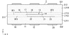
- FIG. 1 is a perspective perspective view of the laminated varistor 1 of the first embodiment
- FIG. 2 is a perspective view of the laminated varistor 1 from above
- FIG. 3 is a cross-sectional view of the laminated varistor 1.
- the laminated varistor 1 includes a sintered body 11, a first external electrode 12, a second external electrode 16, a third external electrode 20, a first internal electrode 13, a second internal electrode 17, and a third internal electrode. 21 and.
- the sintered body 11 excluding the external electrode of the laminated varistor 1 has, for example, a rectangular parallelepiped shape having a length of 1.6 mm, a width of 0.8 mm, and a height of 0.8 mm.
- the corners of the sintered body 11 may be chamfered as appropriate, and the sintered body 11 may be chamfered.
- the corners may be rounded.
- the X-axis direction parallel to the long side direction of the sintered body 11 is defined as the left-right direction
- the Y-axis direction is defined as the front-rear direction (depth direction)
- the Z-axis direction is defined as the vertical direction. ..
- the positive direction in the X-axis direction is defined as the right side
- the positive direction in the Y-axis direction is defined as the front side
- the positive direction in the Z-axis direction is defined as the upper side.
- these directions are examples, and are not intended to limit the directions when the laminated varistor 1 is used.
- the arrows indicating each direction in the drawing are shown only for the sake of explanation, and are not accompanied by an entity.
- the sintered body 11 has a first end surface S11 and a second end surface S12 facing each other in the first direction, and a first side surface S21 and a second side surface S22 facing each other in the second direction. Further, it has a first main surface S31 and a second main surface S32 facing each other in the third direction.
- the sintered body 11 has a laminated structure in which a plurality of layers LY11 to LY14 (see FIG. 3) are laminated in a third direction, and is formed in a rectangular parallelepiped shape having a long side in the first direction.
- the sintered body 11 is composed of a semiconductor ceramic component having non-linear resistance characteristics.
- the sintered body 11 may contain, for example, ZnO as a main component and at least one of Bi 2 O 3 , Co 2 O 3 , MnO 2 , and Sb 2 O 3 as a sub component, and Pr 6 O 11 may be contained. , Co 2 O 3 , CaCO 3 , and Cr 2 O 3 may be contained.
- ZnO is sintered and other subcomponents are precipitated at the grain boundaries thereof, and an internal electrode is formed between the layers. Then, the non-linear resistance characteristic is exhibited by the grain boundary barrier formed between the ZnO particles.
- the sintered body 11 is formed, for example, by laminating four layers LY11 to LY14 (see FIG. 3) containing ZnO as a main component and then sintering the layers.
- a first external electrode 12 is provided at the center of the side surface on the long side of the sintered body 11.
- the first external electrode 12 is electrically connected to the first internal electrode 13.
- the sintered body 11 is provided with two first external electrodes 12, one of the two first external electrodes 12 is provided on the first side surface S21, and the other of the two first external electrodes 12. Is provided on the second side surface S22.
- the two first external electrodes 12 are electrically connected via the first internal electrode 13.
- a second external electrode 16 and a third external electrode 20 are provided on both sides of the first external electrode 12.
- the second external electrode 16 and the third external electrode 20 are provided on both sides of each of the two first external electrodes 12. That is, the first side surface S21 is provided with the second external electrode 16 and the third external electrode 20 on both sides of the first external electrode 12, and the second side surface S22 is provided with the second outside on both sides of the first external electrode 12.
- the electrode 16 and the third external electrode 20 are provided.
- the sintered body 11 is provided with two second external electrodes 16, one of the two second external electrodes 16 is provided on the first side surface S21, and the other of the two second external electrodes 16 is provided. It is provided on the second side surface S22.
- the sintered body 11 is provided with two third external electrodes 20, one of the two third external electrodes 20 is provided on the first side surface S21, and the other of the two third external electrodes 20 is provided. It is provided on the second side surface S22.
- a second internal electrode 17 electrically connected to the second external electrode 16 and a third internal electrode 21 electrically connected to the third external electrode 20 are provided inside the sintered body 11, a second internal electrode 17 electrically connected to the second external electrode 16 and a third internal electrode 21 electrically connected to the third external electrode 20 are provided. ..
- the second external electrode 16 is electrically connected to the second internal electrode 17, and the third external electrode 20 is electrically connected to the third internal electrode 21. That is, the two second external electrodes 16 provided on the sintered body 11 are electrically connected via the second internal electrode 17, and the two third external electrodes 20 provided on the sintered body 11 are electrically connected to each other. It is electrically connected via the third internal electrode 21.
- the sintered body 11 is formed by laminating, for example, four layers LY11 to LY14 in the third direction (see FIG. 3).
- the first internal electrode 13 is provided by printing on, for example, the upper surface of the layer LY12 (hereinafter, also referred to as the first laminated surface SF1) among the four layers LY11 to LY14.
- the second internal electrode 17 is provided, for example, on the upper surface of the layer LY13 laminated on the upper side of the layer LY12 (hereinafter, also referred to as the second laminated surface SF2) by printing.
- the third internal electrode 21 is provided, for example, on the upper surface of the layer LY11 laminated on the lower side of the layer LY12 (hereinafter, also referred to as the third laminated surface SF3) by printing.
- the first internal electrode 13 is provided on the first laminated surface SF1 inside the sintered body 11.
- the second internal electrode 17 is provided inside the sintered body 11 on a second laminated surface SF2 different from the first laminated surface SF1.
- the third internal electrode 21 is provided inside the sintered body 11 on a third laminated surface SF3 different from the first laminated surface SF1 and the second laminated surface SF2.
- the first internal electrode 13 is arranged between the second internal electrode 17 and the third internal electrode 21.
- the first internal electrode 13 has a first facing portion 14 and a first drawing portion 15.
- the width of the first drawer portion 15 is narrower than that of the first facing portion 14.
- the first drawer portion 15 projects from the first facing portion 14 along the second direction.
- two first drawer portions 15 project from the first facing portion 14 toward the front side and the rear side.
- One of the two first drawers 15 is electrically connected to the first external electrode 12 provided on the first side surface S21, and the other of the two first drawers 15 is provided on the second side surface S22. It is electrically connected to the first external electrode 12.
- the second internal electrode 17 has a second facing portion 18 and a second lead-out portion 19.
- the width of the second drawer portion 19 is narrower than that of the second facing portion 18.
- the second drawer portion 19 projects from the second facing portion 18 along the first direction.
- the second drawer portion 19 has a first connecting portion 19B that connects between the two second external electrodes 16 and a second facing portion 18 along the first direction. It has a first protruding portion 19A that protrudes and is connected to the first connecting portion 19B.
- the first protruding portion 19A protrudes from the second facing portion 18, for example, to the left.
- the first connecting portion 19B projects from the left end portion of the first protruding portion 19A to the front side and the rear side, respectively, and connects between the two second external electrodes 16.
- the third internal electrode 21 has a third facing portion 22 and a third lead-out portion 23.
- the width of the third drawer portion 23 is narrower than that of the third facing portion 22.
- the third drawer portion 23 projects from the third facing portion 22 along the first direction. In the present embodiment, the third drawer portion 23 projects in the opposite direction to the second drawer portion 19, for example, to the right.
- the third lead-out portion 23 has a second connecting portion 23B that connects between the two third external electrodes 20, and a second connecting portion 23 that protrudes from the third facing portion 22 along the first direction. It has a second protruding portion 23A connected to the portion 23B.
- the second protruding portion 23A protrudes from the third facing portion 22, for example, to the right.
- the second connecting portion 23B projects from the right end portion of the second protruding portion 23A to the front side and the rear side, respectively, and connects between the two third external electrodes 20.
- the first internal electrode 13 is formed on the first laminated surface SF1
- the second internal electrode 17 is formed on the second laminated surface SF2
- the third internal electrode 21 is formed on the third laminated surface SF3.
- the 1 internal electrode 13, the 2nd internal electrode 17, and the 3rd internal electrode 21 are all arranged along the second direction.
- the length of the first facing portion 14 is longer than the length of the second facing portion 18 and the third facing portion 22. Further, in the second direction, the length of the first facing portion 14 is longer than the length of the second facing portion 18 and the third facing portion 22. Therefore, the area of the first facing portion 14 is larger than the area of the second facing portion 18 and the third facing portion 22. Since such a first facing portion 14 is arranged between the second facing portion 18 and the third facing portion 22, the stray capacitance generated between the second facing portion 18 and the third facing portion 22 is reduced. Therefore, crosstalk can be suppressed.
- the two first external electrodes 12, the two second external electrodes 16, and the two third external electrodes 20 have long sides when the sintered body 11 is viewed from the stacking direction. It is provided on both side surfaces (first side surface S21 and second side surface S22). In the first direction, since the first external electrode 12 exists between the second external electrode 16 and the third external electrode 20, the stray capacitance between the second external electrode 16 and the third external electrode 20 can be reduced. Further, the two first external electrodes 12, the two second external electrodes 16, and the two third external electrodes 20 are connected by the first drawer portion 15, the second drawer portion 19, and the third drawer portion 23, respectively. Has been done.
- the first external electrode 12, the second external electrode 16, and the third external electrode 20 can be formed at the same time, the process can be simplified, and the shape can be stably provided. It is possible to obtain a laminated varistor 1 having less variation in characteristics.
- the first internal electrode 13 is provided so as to be sandwiched between the second internal electrode 17 and the third internal electrode 21 in the stacking direction of the sintered body 11. That is, the first internal electrode 13 exists between the second internal electrode 17 and the third internal electrode 21 in the third direction. Specifically, the first facing portion 14 exists between the second internal electrode 17 and the third internal electrode 21. In other words, the second facing portion 18 and the third facing portion 22 face each other, and the first internal electrode 13 exists between the second facing portion 18 and the third facing portion 22. Therefore, the first facing portion 14 exists between the second facing portion 18 and the third facing portion 22.
- the varistor region is formed by the second facing portion 18 and the first facing portion 14 facing each other, and the first facing portion 14 and the third facing portion 22 facing each other.
- FIG. 5 is a schematic circuit diagram showing a usage example of the laminated varistor 1 of the present embodiment.
- the laminated varistor 1 of the present embodiment is composed of a first varistor 1A composed of a first external electrode 12 and a second external electrode 16, and a first external electrode 12 and a third external electrode 20. It has a second varistor 1B and the like.
- the circuit diagram of FIG. 5 shows a state in which the laminated varistor 1 is arranged in the vicinity of the communication IC 2 that communicates by the two-wire differential voltage transmission method.
- the land of the signal lines 3 and 4 and the land of the ground line 5 are connected to the communication IC 2.
- the pair of first external electrodes 12 on the first side surface S21 and the second side surface S22 are connected to the land of the ground line 5, respectively, and the pair of second external electrodes 16 on the first side surface S21 and the second side surface S22 are connected to each other.
- Each is connected to the land of the signal line 3
- the pair of third external electrodes 20 on the first side surface S21 and the second side surface S22 are connected to the land of the signal line 4, respectively.
- the first facing portion 14 is, for example, a rectangle of 0.46 mm ⁇ 0.20 mm
- the second facing portion 18 and the third facing portion 22 are, for example, a rectangle of 0.40 mm ⁇ 0.14 mm. It has become.
- the first facing portion 14 and the second facing portion 18 face each other at a distance of, for example, 0.035 mm.
- the first facing portion 14 and the third facing portion 22 face each other at a distance of, for example, 0.035 mm.
- the centers of each are at the same position when viewed from the stacking direction.
- the first facing portion 14 protrudes 0.03 mm from the second facing portion 18 and the third facing portion 22 and covers the entire circumference of the second facing portion 18 and the third facing portion 22. It is in a state of being. In other words, when viewed from the third direction, the first facing portion 14 covers the outer circumferences of the second facing portion 18 and the third facing portion 22. By doing so, it is possible to prevent stray capacitance from being generated between the second facing portion 18 and the third facing portion 22, and to suppress crosstalk. It should be noted that each of the above dimensions is an example and can be changed as appropriate.
- a second drawing portion 19 having a width of 0.1 mm extends and is connected to the second external electrode 16.
- a third drawer portion 23 having a width of 0.1 mm extends and is connected to the third external electrode 20.
- a first drawing portion 15 having a width of 0.1 mm extends and is connected to the first external electrode 12. Since the lead portion having a width narrower than that of the facing portion is connected to the external electrode in this way, the stray capacitance between the second external electrode 16 and the third external electrode 20 can be reduced, and crosstalk can be achieved. The impact can be minimized.
- the width of the second drawer portion 19 is 90% or less of the width of the second facing portion 18. Further, in the second direction, it is more desirable that the width of the second drawer portion 19 is 70% or less of the width of the second facing portion 18. Similarly, in the second direction, it is desirable that the width of the third drawer portion 23 is 90% or less of the width of the third facing portion 22. Further, in the second direction, it is more desirable that the width of the second drawer portion 19 is 70% or less of the width of the second facing portion 18. On the contrary, when the widths of the second drawer portion 19 and the third drawer portion 23 are larger than 90% of the widths of the second facing portion 18 and the third facing portion 22, respectively, the stray capacitance affecting the crosstalk becomes large.
- the width of the second drawer portion 19 is set to 90% or less of the width of the second facing portion 18 in the second direction.
- the stray capacitance generated in the first varistor 1A is reduced and the occurrence of crosstalk is suppressed. can.
- the width of the third drawer portion 23 is set to 90% or less of the width of the third facing portion 22 in the second direction, the stray capacitance generated in the second varistor 1B is reduced and the occurrence of crosstalk is suppressed. can.
- the absolute value of the difference between the stray capacitance of the first varistor 1A and the stray capacitance of the second varistor 1B can be reduced to suppress crosstalk.
- the width of the second drawer portion 19 is preferably 0.08 mm or more, and more preferably 0.1 mm or more.
- the width of the third drawer 23 is preferably 0.08 mm or more, and more preferably 0.1 mm or more.
- the width of the first drawer portion 15 is 90% or less of the width of the first facing portion 14. Further, it is more desirable that the width of the first drawer portion 15 is 70% or less of the width of the first facing portion 14 in the first direction.
- the width of the first drawer portion 15 is 0.08 mm or more, and more preferably 0.1 mm or more. This has the advantage that the shape of the first drawer portion 15 can be easily maintained.
- the size of the first facing portion 14 protruding from the outer periphery of the second facing portion 18 and the third facing portion 22 in the first direction is the length of the second facing portion 18 and the third facing portion 22. It is desirable that it is 7.5% or more and 15% or less with respect to the side. In other words, in the first direction, the length of the first facing portion 14 is preferably 107.5% or more and 115% or less of the length of the second facing portion 18 or the third facing portion 22.
- the amount of protrusion of the first facing portion 14 is smaller than 7.5% with respect to the long sides of the second facing portion 18 and the third facing portion 22, the crosstalk increases sharply, and when it becomes larger than 15%, it is manufactured.
- the length of the first facing portion 14 is more preferably 9% or more and 13.5% or less of the length of the second facing portion 18 or the third facing portion 22, and is more preferably crosstalk. Can be further reduced, and the deviation in manufacturing can be alleviated.
- the length of the first facing portion 14 is preferably 107.5% or more and 115% or less of the length of the second facing portion 18 or the third facing portion 22.
- the amount of protrusion of the first facing portion 14 is smaller than 7.5% with respect to the long sides of the second facing portion 18 and the third facing portion 22, the crosstalk increases sharply, and when it becomes larger than 15%, it is manufactured. This is because the above deviation cannot be alleviated and the capacity difference between the first varistor 1A and the second varistor 1B becomes large.
- the volume of the region sandwiched between the first facing portion 14 and the second facing portion 18 is preferably 5% or less of the volume of the entire sintered body 11 and is preferably 1% or less. It is desirable to do. When it is larger than 1%, the entire varistor region is in close proximity to the external electrode, so that the capacitance that affects crosstalk increases.
- the area of the first facing portion 14 is larger than the area of the second facing portion 18 or the third facing portion 22.
- the first to third internal electrodes 13, so that the area of the first facing portion 14 is larger than the area of the second facing portion 18 and larger than the area of the third facing portion 22. 17, 21 are formed.
- the first facing portion 14 of the first internal electrode 13 is the third facing portion 18 of the second internal electrode 17 and the third facing portion 22 of the third internal electrode 21 inside the sintered body 11, respectively. They are arranged at overlapping positions in the direction. That is, the first internal electrode 13 has a superposed region A1 (see FIG. 2) that overlaps with the second internal electrode 17 and the third internal electrode 21 in the third direction.
- the superimposed region A1 is a rectangular region whose longitudinal direction is the first direction.
- the length L1 of the superimposing region A1 in the first direction is longer than the length L2 of the superimposing region A1 in the second direction.
- the laminated varistor 1 of the present embodiment includes the first varistor 1A and the second varistor 1B
- the capacitances of the first varistor 1A and the second varistor 1B are 200 pF or less, respectively.
- the difference between the capacitance of the first varistor 1A and the capacitance of the second varistor 1B is preferably ⁇ 20% or more and + 20% or less of the capacitance of the first varistor 1A.
- FIG. 6 is a perspective perspective view of the laminated varistor 1 of the second embodiment
- FIG. 7 is an external perspective view of the laminated varistor 1 of the second embodiment.
- the second external electrode 16 and the third external electrode 20 are provided on both side surfaces which are long sides, whereas in the laminated varistor 1 of the second embodiment, the sintered body 11 is provided.
- the second external electrode 16 is provided on the first end surface S11
- the third external electrode 20 is provided on the second end surface S12 of the sintered body 11. Since the configurations of the first internal electrode 13, the second internal electrode 17, and the third internal electrode 21 are the same as those in the first embodiment, the common components are designated by the same reference numerals and the description thereof will be omitted. ..
- the first external electrode 12 is provided on a part of the first side surface S21 and a part of the second side surface S22.
- the second external electrode 16 is provided on at least a part of the first end surface S11.
- the second external electrode 16 is provided on the entire first end surface S11, from the first end surface S11 to a part of the first side surface S21 and the second side surface S22, and the first main surface S31 and the second main surface. It is provided over a part of S32.
- the third external electrode 20 is provided on at least a part of the second end surface S12.
- the third external electrode 20 is provided on the entire second end surface S12, from the second end surface S12 to a part of the first side surface S21 and the second side surface S22, and the first main surface S31 and the second main surface. It is provided over a part of S32.
- the second external electrode 16 is provided from the first end surface S11 to a part of the first side surface S21, the second side surface S22, the first main surface S31, and the second main surface S32. Therefore, the distance between the second external electrode 16 and the first external electrode 12 can be made wider than that of the laminated varistor 1 of the first embodiment, and the second external electrode 16 and the first external electrode 12 can be obtained. The floating capacity between can be reduced.
- the third external electrode 20 is provided from the second end surface S12 to a part of the first side surface S21, the second side surface S22, the first main surface S31, and the second main surface S32. Therefore, the distance between the third external electrode 20 and the first external electrode 12 can be made wider than that of the laminated varistor 1 of the first embodiment, and the third external electrode 20 and the first external electrode 12 can be obtained. The floating capacity between can be reduced.
- the second external electrode 16 and the third external electrode 20 are provided.
- the distance between 20 and 20 can be increased as compared with the laminated varistor 1 of the first embodiment, and the influence on the crosstalk can be further reduced.
- FIG. 8 is a perspective perspective view of the laminated varistor 1 of the third embodiment
- FIG. 9 is a perspective top view of the laminated varistor 1 of the third embodiment
- FIG. 10 is a cross-sectional view of the laminated varistor 1 of the third embodiment.
- the first facing portion 14 covers the outer periphery of the second facing portion 18 and the third facing portion 22, whereas in the third embodiment, it is shown in FIGS. 9 and 10.
- a part of the second facing portion 18 and the third facing portion 22 projects to the outside of the first facing portion 14. Since the components other than the first internal electrode 13, the second internal electrode 17, and the third internal electrode 21 have the same configuration as that of the laminated varistor 1 of the second embodiment, the components common to the second embodiment may be included. The same reference numerals are given, and the description thereof will be omitted.
- the second facing portion 18 is formed in a rectangular shape with the first direction as the longitudinal direction.
- the length of the second facing portion 18 in the first direction is longer than the length of the first facing portion 14 in the first direction, and the length of the second facing portion 18 in the second direction is the first of the first facing portions 14. Shorter than the length in two directions.
- the third facing portion 22 is formed in a rectangular shape with the first direction as the longitudinal direction.
- the length of the third facing portion 22 in the first direction is longer than the length of the first facing portion 14 in the first direction, and the length of the third facing portion 22 in the second direction is the length of the first facing portion 14. Shorter than the length in two directions.
- the first facing portion 14 and the second facing portion 18 face each other at a predetermined interval, and the first facing portion 14 and the third facing portion 22 face each other at a predetermined interval.
- the centers of the first facing portion 14, the second facing portion 18, and the third facing portion 22 are at the same position when viewed from the stacking direction, and the second facing portion 18 and the third facing portion 22 are viewed from the stacking direction. Almost overlap. Further, when viewed from the stacking direction, in the first direction, the right end and the left end of the second facing portion 18 protrude from the first facing portion 14, and the right end and the left end of the third facing portion 22 are the first facing portions. It sticks out of 14.
- the second facing portion 18 is covered with the first facing portion 14 except for the protruding portions at the right end and the left end.
- the third facing portion 22 is covered with the first facing portion 14 except for the protruding portions at the right end and the left end.
- the first internal electrode 13 is placed with respect to the second internal electrode 17 and the third internal electrode 21.
- the position may shift in the first direction.
- the capacitance generated between the first external electrode 12 and the second external electrode 16 There is a possibility that the capacitance difference with the capacitance generated between the first external electrode 12 and the third external electrode 20 becomes large.
- the second facing portion 18 and the third facing portion 22 are provided so as to protrude from both sides of the first facing portion 14 in the first direction, the second internal electrode 17 and the third are provided. Even when the position of the first internal electrode 13 is displaced in the first direction with respect to the internal electrode 21, the capacitance generated between the first external electrode 12 and the second external electrode 16 and the first external electrode 12 The capacitance difference with the capacitance generated between the third external electrode 20 and the third external electrode 20 can be reduced. Therefore, there is an advantage that crosstalk generated due to the capacitance difference between the first varistor 1A and the second varistor 1B can be suppressed.
- Table 1 below shows the relationship between the ratio of the horizontal dimension (length L1) to the vertical dimension (length L2) of the superposed region A1 and the capacitance difference caused by the variation in the dimensions.
- the dimensional variation is the dimensional variation between the internal electrodes or the dimensional variation between the internal electrode and the external electrode that occurs in each process such as printing, laminating, cutting, and forming the external electrode of the internal electrode. ..
- the capacitance difference is the absolute value of the difference between the stray capacitance generated between the first internal electrode 13 and the second internal electrode 17 and the stray capacitance generated between the first internal electrode 13 and the third internal electrode 21. Is. In Table 1, the capacity difference of Examples 1, 3 and 4 and Comparative Examples 1 and 2 is evaluated with the capacity difference of Example 2 as 1.
- the sintered body 11 has a rectangular shape having a length of 1.6 mm, a width of 0.8 mm, and a height of 0.8 mm
- the first facing portion 14 has a rectangular shape having a length of 0.44 mm and a width of 0.22 mm.
- the second facing portion 18 and the third facing portion 22 have a rectangular shape having a length of 0.54 mm and a width of 0.12 mm.
- the ratio of the length L1 of the superimposed region A1 in the first direction to the length L2 of the superimposed region A1 in the second direction is 1.3 or more and 7.5 or less.
- the difference in capacitance between the first varistor 1A and the second varistor 1B can be reduced to improve the communication quality.
- Table 2 below shows the relationship between the ratio of the area of the overlapping region A1 to the area of the first laminated surface SF1 of the sintered body 11 (area ratio) and the capacity difference generated by the variation in dimensions.
- the dimensional variation is the dimensional variation between the internal electrodes caused in each process such as printing, laminating, cutting, and forming the external electrode of the internal electrode, or the dimensional variation between the internal electrode and the external electrode. That is.
- the capacitance difference is the absolute value of the difference between the stray capacitance generated between the first internal electrode 13 and the second internal electrode 17 and the stray capacitance generated between the first internal electrode 13 and the third internal electrode 21. Is.
- the capacity difference of Examples 5 and 6 and Comparative Examples 3 and 4 is evaluated with the capacity difference of Example 2 as 1.
- the sintered body 11 has a rectangular shape having a length of 1.6 mm, a width of 0.8 mm, and a height of 0.8 mm
- the first facing portion 14 has a rectangular shape having a length of 0.44 mm and a width of 0.22 mm.
- the second facing portion 18 and the third facing portion 22 have a rectangular shape having a length of 0.54 mm and a width of 0.12 mm.
- the ratio of the area of the superimposed region A1 to the cross-sectional area of the sintered body 11 on the first laminated surface SF1 is 0.024 or more and 0.161 or less.
- the difference in capacitance between the first varistor 1A and the second varistor 1B can be reduced to improve the communication quality.
- the first internal electrode 13 overlaps with the second internal electrode 17 and the third internal electrode 21 in the third direction.
- the superimposed region A1 exists in the second region A3 other than the first region A2 on which the first external electrode 12, the second external electrode 16, and the third external electrode 20 are projected on the first laminated surface SF1. ing.
- the stray capacitance generated between the first external electrode 12, the second external electrode 16 and the third external electrode 20 can be reduced, and crosstalk can be suppressed.
- the superimposed region A1 is the first one on which the first external electrode 12, the second external electrode 16, and the third external electrode 20 are projected on the first laminated surface SF1, respectively. It exists in the second region A3 other than the region A2, and the occurrence of crosstalk can be suppressed.
- the first internal electrode 13, the second internal electrode 17, and the third internal electrode 21 of the third embodiment may be applied to the laminated varistor 1 of the first embodiment, which is the same as that of the laminated varistor 1 of the third embodiment. There are advantages.
- one layer each of the second internal electrode 17 and the first internal electrode 13 facing each other and the third internal electrode 21 and the first internal electrode 13 facing each other is one layer.
- they may face each other in multiple layers.
- the second internal electrode 17 and the first internal electrode 13 may face each other in multiple layers, or the third internal electrode 21 and the first internal electrode 13 may have multiple layers. It may be opposed to each other.
- the first external electrode 12, the second external electrode 16, and the third external electrode 20 are provided on each of the first side surface S21 and the second side surface S22.
- the external electrode 12, the second external electrode 16, and the third external electrode 20 may be provided on at least one of the first side surface S21 and the second side surface S22. That is, the first external electrode 12, the second external electrode 16, and the third external electrode 20 may be provided only on one of the first side surface S21 and the second side surface S22.
- the sintered body 11 is formed by laminating four layers LY11 to LY14, but the sintered body 11 is not limited to one having a four-layer laminated structure, and a plurality of layers are laminated. It suffices to have a structure.
- the laminated varistor 1 according to the present disclosure is industrially useful because it is possible to obtain a laminated varistor 1 with suppressed crosstalk by reducing the stray capacitance generated between the external electrodes.
Landscapes
- Engineering & Computer Science (AREA)
- Microelectronics & Electronic Packaging (AREA)
- Physics & Mathematics (AREA)
- Electromagnetism (AREA)
- Thermistors And Varistors (AREA)
Abstract
本開示の課題は、外部端子間に発生するクロストークを抑えた積層バリスタを得ることである。積層バリスタ1は、複数の層が第3方向に積層された積層構造を有する。積層バリスタ1は、第1外部電極12と電気的に接続された第1内部電極13と、第2外部電極16と電気的に接続された第2内部電極17と、第3外部電極20と電気的に接続された第3内部電極21と、を備える。第3方向において、第1内部電極13は、第2内部電極17と第3内部電極21との間に配置されている。
Description
本発明は、各種電子機器に用いられる積層バリスタに関するものである。
近年、家電製品や車載電子機器において小型化が進んでおり、その部品であるバリスタも小型化が求められている。また高周波化が進むと静電容量が性能に影響を与えるため、所定のバリスタ電圧を確保しながら、静電容量が小さく、そのばらつきも小さいバリスタが求められている。またバリスタをペアで使う場合、ペア間の静電容量の差を小さくするために、1素子の中に2個のバリスタを形成したものが提案されている。なお、この出願の発明に関連する先行技術文献情報としては、例として、特許文献1が知られている。
しかしながら従来の積層バリスタでは、バリスタ性能を発揮する内部電極間だけではなく、2個の外部電極の間に浮遊容量が発生する。そのため、2個の外部電極のうちの一方の外部電極から他方の外部電極に信号が漏れるクロストークが発生し、信号波形に乱れが生じる可能性がある。
本開示の一態様の積層バリスタは、焼結体と、第1外部電極と、第2外部電極と、第3外部電極と、第1内部電極と、第2内部電極と、第3内部電極と、を備える。前記焼結体は、第1方向において互いに対向する第1端面及び第2端面、第2方向において互いに対向する第1側面及び第2側面、並びに第3方向おいて互いに対向する第1主面及び第2主面を有する。前記焼結体は、複数の層が前記第3方向に積層された積層構造を有し、前記第1方向を長辺とする直方体状に形成される。前記第1外部電極は、前記第1側面及び前記第2側面の少なくとも一方に設けられている。前記第2外部電極及び前記第3外部電極は、前記第1側面及び前記第2側面の少なくとも一方に設けられ、前記第1外部電極の両側に設けられている。前記第1内部電極は、前記焼結体の内部に設けられ、前記第1外部電極と電気的に接続されている。前記第2内部電極は、前記焼結体の内部に設けられ、前記第2外部電極と電気的に接続されている。前記第3内部電極は、前記焼結体の内部に設けられ、前記第3外部電極と電気的に接続されている。前記第3方向において、前記第1内部電極は、前記第2内部電極と前記第3内部電極との間に配置されている。
(1)実施形態1
以下、本開示の実施形態1における積層バリスタについて、図面を参照しながら説明する。
以下、本開示の実施形態1における積層バリスタについて、図面を参照しながら説明する。
図1は実施形態1の積層バリスタ1の透視斜視図、図2はこの積層バリスタ1の上方からの透視図、図3は積層バリスタ1の断面図である。積層バリスタ1は、焼結体11と、第1外部電極12と、第2外部電極16と、第3外部電極20と、第1内部電極13と、第2内部電極17と、第3内部電極21と、を備えている。この積層バリスタ1の外部電極を除いた焼結体11は、例えば、長さ1.6mm、幅0.8mm、高さ0.8mmの直方体状としている。なお、図3等の外観斜視図において、焼結体11の外形は直方体状に図示されているが、焼結体11の角部には適宜面取り加工を施してもよく、焼結体11の角部は丸みを帯びていてもよい。
以下の説明では、図1に示すように、焼結体11の長辺方向と平行なX軸方向を左右方向、Y軸方向を前後方向(奥行き方向)、Z軸方向を上下方向と規定する。さらに、X軸方向の正の向きを右側、Y軸方向の正の向きを前側、Z軸方向の正の向きを上側と規定する。ただし、これらの方向は一例であり、積層バリスタ1の使用時の方向を限定する趣旨ではない。また、図面中の各方向を示す矢印は説明のために表記しているに過ぎず、実体を伴わない。
焼結体11は、図2及び図3に示すように、第1方向において互いに対向する第1端面S11及び第2端面S12、第2方向において互いに対向する第1側面S21及び第2側面S22、並びに第3方向おいて互いに対向する第1主面S31及び第2主面S32を有する。焼結体11は、複数の層LY11~LY14(図3参照)が第3方向に積層された積層構造を有しており、第1方向を長辺とする直方体状に形成されている。
焼結体11は、非直線性抵抗特性を有する半導体セラミックス成分で構成されている。この焼結体11は、例えば、ZnOを主成分とし、副成分としてBi2O3、Co2O3、MnO2、Sb2O3のうちの少なくとも1種を含んでもよく、Pr6O11、Co2O3、CaCO3、Cr2O3のうちの少なくとも1種を含んでもよい。焼結体11は、ZnOが焼結し、その粒界にその他の副成分が析出した形になり、積層間に内部電極が形成されている。そして、ZnO粒子間に形成される粒界障壁により非直線性抵抗特性が発現する。焼結体11は、例えば、ZnOを主成分とする4つの層LY11~LY14(図3参照)を積層した後に焼結して形成されている。
焼結体11の長辺側側面の中央部には第1外部電極12が設けられている。第1外部電極12は、第1内部電極13と電気的に接続されている。本実施形態では、焼結体11に2つの第1外部電極12が設けられており、2つの第1外部電極12の一方は第1側面S21に設けられ、2つの第1外部電極12の他方は第2側面S22に設けられている。2つの第1外部電極12は、第1内部電極13を介して電気的に接続されている。
第1外部電極12の両側には、第2外部電極16及び第3外部電極20が設けられている。本実施形態では、2つの第1外部電極12の各々の両側に、第2外部電極16及び第3外部電極20が設けられている。つまり、第1側面S21には、第1外部電極12の両側に第2外部電極16及び第3外部電極20が設けられ、第2側面S22には、第1外部電極12の両側に第2外部電極16及び第3外部電極20が設けられている。言い換えると、焼結体11には2つの第2外部電極16が設けられており、2つの第2外部電極16の一方は第1側面S21に設けられ、2つの第2外部電極16の他方は第2側面S22に設けられている。同様に、焼結体11には2つの第3外部電極20が設けられており、2つの第3外部電極20の一方は第1側面S21に設けられ、2つの第3外部電極20の他方は第2側面S22に設けられている。
焼結体11の内部には、第2外部電極16と電気的に接続された第2内部電極17及び、第3外部電極20と電気的に接続された第3内部電極21が設けられている。第2外部電極16は第2内部電極17に電気的に接続され、第3外部電極20は第3内部電極21に電気的に接続されている。つまり、焼結体11に設けられた2つの第2外部電極16は第2内部電極17を介して電気的に接続されており、焼結体11に設けられた2つの第3外部電極20は第3内部電極21を介して電気的に接続されている。
本実施形態では、焼結体11が例えば4つの層LY11~LY14を第3方向に積層して形成されている(図3参照)。第1内部電極13は、4つの層LY11~LY14のうち例えば層LY12の上面(以下、第1積層面SF1とも言う。)に、印刷により設けられている。第2内部電極17は、例えば、層LY12の上側に積層されている層LY13の上面(以下、第2積層面SF2とも言う。)に、印刷により設けられている。第3内部電極21は、例えば、層LY12の下側に積層されている層LY11の上面(以下、第3積層面SF3とも言う。)に、印刷により設けられている。言い換えると、第1内部電極13は、焼結体11の内部において、第1積層面SF1に設けられている。第2内部電極17は、焼結体11の内部において、第1積層面SF1と異なる第2積層面SF2に設けられている。第3内部電極21は、焼結体11の内部において、第1積層面SF1及び第2積層面SF2と異なる第3積層面SF3に設けられている。これにより、第3方向(上下方向)において、第1内部電極13は、第2内部電極17と第3内部電極21との間に配置されている。
第1内部電極13は第1対向部14と第1引き出し部15とを有している。第1引き出し部15は、第1対向部14よりも幅が狭い。第1引き出し部15は、第1対向部14から第2方向に沿って突出している。本実施形態では第1対向部14から前側及び後側に向かって2つの第1引き出し部15が突出している。2つの第1引き出し部15の一方は、第1側面S21に設けられた第1外部電極12に電気的に接続され、2つの第1引き出し部15の他方は、第2側面S22に設けられた第1外部電極12に電気的に接続されている。
第2内部電極17は第2対向部18と第2引き出し部19とを有している。第2引き出し部19は、第2対向部18よりも幅が狭い。第2引き出し部19は、第2対向部18から第1方向に沿って突出している。本実施形態では、第2引き出し部19は、図2に示すように、2つの第2外部電極16の間を連結する第1連結部19Bと、第2対向部18から第1方向に沿って突出して第1連結部19Bに接続される第1突出部19Aと、を有している。ここで、第1突出部19Aは第2対向部18から例えば左向きに突出している。第1連結部19Bは、第1突出部19Aの左端部から前側及び後側にそれぞれ突出して、2つの第2外部電極16の間を連結する。
第3内部電極21は第3対向部22と第3引き出し部23とを有している。第3引き出し部23は、第3対向部22よりも幅が狭い。第3引き出し部23は、第3対向部22から第1方向に沿って突出している。本実施形態では、第3引き出し部23は、第2引き出し部19と反対向き、例えば右向きに突出している。第3引き出し部23は、図2に示すように、2つの第3外部電極20の間を連結する第2連結部23Bと、第3対向部22から第1方向に沿って突出して第2連結部23Bに接続される第2突出部23Aと、を有している。ここで、第2突出部23Aは第3対向部22から例えば右向きに突出している。第2連結部23Bは、第2突出部23Aの右端部から前側及び後側にそれぞれ突出して、2つの第3外部電極20の間を連結する。
ここで、第1内部電極13は第1積層面SF1に、第2内部電極17は第2積層面SF2に、第3内部電極21は第3積層面SF3に、それぞれ、形成されており、第1内部電極13、第2内部電極17、及び第3内部電極21は、いずれも第2方向に沿って配置されている。
ここにおいて、第1方向において、第1対向部14の長さは、第2対向部18及び第3対向部22の長さよりも長い。また、第2方向において、第1対向部14の長さは、第2対向部18及び第3対向部22の長さよりも長い。したがって、第1対向部14の面積は、第2対向部18及び第3対向部22の面積よりも大きくなっている。このような第1対向部14が第2対向部18及び第3対向部22の間に配置されているので、第2対向部18と第3対向部22との間に発生する浮遊容量を低減して、クロストークを抑制することができる。
上述のように、本実施形態では、2つの第1外部電極12、2つの第2外部電極16、及び2つの第3外部電極20は、焼結体11を積層方向から見たときの長辺となる両側面(第1側面S21及び第2側面S22)にそれぞれ設けられている。第1方向において、第1外部電極12は、第2外部電極16及び第3外部電極20の間に存在するので、第2外部電極16と第3外部電極20の間の浮遊容量を低減できる。また、2つの第1外部電極12、2つの第2外部電極16、及び2つの第3外部電極20は、それぞれ第1引き出し部15、第2引き出し部19、及び第3引き出し部23によって、連結されている。このように構成することにより、第1外部電極12、第2外部電極16、及び第3外部電極20を同時に形成することができ、工程の簡略化を図るとともに、形状も安定して設けることができ、特性にばらつきの少ない積層バリスタ1を得ることができる。
また、第1内部電極13は焼結体11の積層方向に対して第2内部電極17と第3内部電極21との間に挟まれるように設けられている。つまり、第1内部電極13は第3方向において第2内部電極17と第3内部電極21との間に存在する。具体的には、第1対向部14は、第2内部電極17と第3内部電極21との間に存在する。換言すると、第2対向部18と第3対向部22とが互いに対向しており、第2対向部18と第3対向部22との間に第1内部電極13が存在している。したがって、第1対向部14は、第2対向部18と第3対向部22との間に存在する。第2対向部18と第1対向部14、及び第1対向部14と第3対向部22がそれぞれ対向することによりバリスタ領域を形成している。
図5は本実施形態の積層バリスタ1の使用例を示す模式的な回路図である。本実施形態の積層バリスタ1は、第1外部電極12と第2外部電極16との間で構成される第1バリスタ1Aと、第1外部電極12と第3外部電極20との間で構成される第2バリスタ1Bと、を有している。図5の回路図は、2線式差動電圧伝送方式で通信を行う通信用IC2の近傍に積層バリスタ1が配置された状態を示している。通信用IC2には信号ライン3,4のランドと、グランドライン5のランドが接続されている。そして、第1側面S21及び第2側面S22にある一対の第1外部電極12はそれぞれグランドライン5のランドに接続され、第1側面S21及び第2側面S22にある一対の第2外部電極16はそれぞれ信号ライン3のランドに接続され、第1側面S21及び第2側面S22にある一対の第3外部電極20はそれぞれ信号ライン4のランドに接続されている。このような回路において例えば信号ライン3に静電気が重畳し、第1バリスタ1Aに所定のしきい値電圧を超える電圧が印加されると、第1バリスタ1Aの電気抵抗が急減し、第1バリスタ1Aを介して電流が流れるので、通信用IC2を保護することができる。なお、図5に示す回路は積層バリスタ1を適用する回路の一例であり、適宜変更が可能である。
本実施形態の積層バリスタ1では、第1対向部14は例えば0.46mm×0.20mmの長方形であり、第2対向部18及び第3対向部22は例えば0.40mm×0.14mmの長方形となっている。また第1対向部14と第2対向部18とは例えば0.035mmの間隔で対向している。同様に第1対向部14と第3対向部22とは例えば0.035mmの間隔で対向している。ここでそれぞれの中心は積層方向から見て同じ位置となっている。すなわち積層方向から見たときには、第1対向部14が第2対向部18及び第3対向部22よりも0.03mmはみ出して、第2対向部18及び第3対向部22の周囲全体を覆っている状態となっている。言い換えると、第3方向から見たとき、第1対向部14は、第2対向部18及び第3対向部22の外周を覆っている。このようにすることにより、第2対向部18と第3対向部22との間に浮遊容量が発生することを防止し、クロストークを抑えることができる。なお、上記の各寸法は一例であって、適宜変更が可能である。
第2対向部18からは、例えば幅0.1mmの第2引き出し部19が延びて第2外部電極16に接続されている。同様に第3対向部22からは、例えば幅0.1mmの第3引き出し部23が延びて第3外部電極20に接続されている。また、第1対向部14からは、例えば幅0.1mmの第1引き出し部15が延びて第1外部電極12に接続されている。このように対向部よりも幅の狭い引き出し部により外部電極に接続されているため、第2外部電極16と第3外部電極20との間の浮遊容量を小さくすることができ、クロストークへの影響を最小限にすることができる。
ここで、第2方向において、第2引き出し部19の幅は、第2対向部18の幅の90%以下とすることが望ましい。更に言えば、第2方向において、第2引き出し部19の幅は、第2対向部18の幅の70%以下とするのがより望ましい。同様に、第2方向において、第3引き出し部23の幅は、第3対向部22の幅の90%以下とすることが望ましい。更に言えば、第2方向において、第2引き出し部19の幅は、第2対向部18の幅の70%以下とするのがより望ましい。逆に、第2引き出し部19及び第3引き出し部23の幅が、それぞれ、第2対向部18及び第3対向部22の幅の90%よりも大きくなると、クロストークに影響する浮遊容量が大きくなるため望ましくない。また、第2方向において第2引き出し部19の幅を第2対向部18の幅の90%以下とすることで、第1バリスタ1Aに発生する浮遊容量を低減して、クロストークの発生を抑制できる。また、第2方向において第3引き出し部23の幅を第3対向部22の幅の90%以下とすることで、第2バリスタ1Bに発生する浮遊容量を低減して、クロストークの発生を抑制できる。また、第1バリスタ1Aの浮遊容量と第2バリスタ1Bの浮遊容量の差の絶対値を低減して、クロストークを抑制することができる。
また、第2方向において、第2引き出し部19の幅は、0.08mm以上とすることが望ましく、0.1mm以上とするのがより望ましい。同様に、第2方向において、第3引き出し部23の幅は、0.08mm以上とすることが望ましく、0.1mm以上とするのがより望ましい。第2引き出し部19及び第3引き出し部23の幅が0.08mmよりも小さくなると、第2引き出し部19及び第3引き出し部23の形状が不安定になりやすく、第2外部電極16及び第3外部電極20との接続が不安定になりやすい。第2引き出し部19及び第3引き出し部23の幅を0.08mm以上とすることで、第2引き出し部19及び第3引き出し部23の形状を保ちやすくなるとの利点がある。
また、第1方向において、第1引き出し部15の幅を第1対向部14の幅の90%以下とすることが望ましい。更に言えば、第1方向において、第1引き出し部15の幅を第1対向部14の幅の70%以下とするのがより望ましい。第1方向において第1引き出し部15の幅を第1対向部14の幅の90%以下とすることで、浮遊容量を低減して、クロストークの発生を抑制できる。また、第1方向において、第1引き出し部15の幅を0.08mm以上とすることが望ましく、0.1mm以上とするのがより望ましい。これにより、第1引き出し部15の形状を保ち易くなるという利点がある。
また上面視したときに、第1方向において、第2対向部18及び第3対向部22の外周から第1対向部14がはみ出す大きさは、第2対向部18及び第3対向部22の長辺に対して7.5%以上、15%以下とすることが望ましい。言い換えると、第1方向において、第1対向部14の長さは、第2対向部18又は第3対向部22の長さの107.5%以上、115%以下であることが好ましい。第1対向部14のはみ出し量が、第2対向部18及び第3対向部22の長辺に対して7.5%よりも小さくなるとクロストークが急激に増大し、15%よりも大きくなると製造上のズレを緩和できず、第1バリスタ1Aと第2バリスタ1Bとの容量差が大きくなるからである。なお、第1方向において、第1対向部14の長さは、第2対向部18又は第3対向部22の長さの9%以上、13.5%以下であることがより好ましく、クロストークを更に低減でき、また製造上のズレを緩和できる。
なお、第2方向において、第1対向部14の長さは、第2対向部18又は第3対向部22の長さの107.5%以上、115%以下であることが好ましい。第1対向部14のはみ出し量が、第2対向部18及び第3対向部22の長辺に対して7.5%よりも小さくなるとクロストークが急激に増大し、15%よりも大きくなると製造上のズレを緩和できず、第1バリスタ1Aと第2バリスタ1Bとの容量差が大きくなるからである。
さらに、焼結体11において、第1対向部14と第2対向部18とに挟まれた領域の体積は、焼結体11全体の体積の5%以下とすることが好ましく、1%以下とすることが望ましい。1%よりも大きくなる場合、バリスタ領域全体が外部電極と近接することで、クロストークに影響する容量が大きくなるためである。
また、第1対向部14の面積は、第2対向部18又は第3対向部22の面積よりも大きいことが好ましい。本実施形態では、第1対向部14の面積は、第2対向部18の面積よりも大きく、かつ、第3対向部22の面積よりも大きくなるように、第1~第3内部電極13,17,21が形成されている。
ところで、第1内部電極13の第1対向部14は、焼結体11の内部において、第2内部電極17の第2対向部18及び第3内部電極21の第3対向部22とそれぞれ第3方向において重なる位置に配置されている。つまり、第1内部電極13は、第3方向において、第2内部電極17及び第3内部電極21と重なる重畳領域A1(図2参照)を有している。
重畳領域A1は第1方向を長手方向とする長方形状の領域である。重畳領域A1の第1方向の長さL1は、重畳領域A1の第2方向の長さL2よりも長い。第1方向の長さL1を第2方向の長さL2よりも長くすることで、第1対向部14を挟むように配置されている第2対向部18と第3対向部22との間に発生する浮遊容量を低減して、クロストークを抑えることができる。
また、本実施形態の積層バリスタ1は第1バリスタ1Aと第2バリスタ1Bとを備えているが、第1バリスタ1A及び第2バリスタ1Bの静電容量はそれぞれ200pF以下であることが好ましい。また、第1バリスタ1Aの静電容量と第2バリスタ1Bの静電容量との差は、第1バリスタ1Aの静電容量の-20%以上かつ+20%以下であることが好ましい。これにより、積層バリスタ1を図5に示すような通信用IC2に接続する場合に、クロストークを抑制して、通信品質を向上させることができる。
(2)実施形態2
以下、実施形態2の積層バリスタ1を図6及び図7に基づいて説明する。
以下、実施形態2の積層バリスタ1を図6及び図7に基づいて説明する。
図6は実施形態2の積層バリスタ1の透視斜視図であり、図7は実施形態2の積層バリスタ1の外観斜視図である。
実施形態1の積層バリスタ1では、長辺となる両側面に第2外部電極16と第3外部電極20を設けているのに対して、実施形態2の積層バリスタ1では、焼結体11の第1端面S11に第2外部電極16が設けられ、焼結体11の第2端面S12に第3外部電極20が設けられている。なお、第1内部電極13、第2内部電極17、及び第3内部電極21の構成は実施形態1と同様であるので、共通する構成要素には同一の符号を付してその説明は省略する。
実施形態2の積層バリスタ1では、第1外部電極12が、第1側面S21の一部と、第2側面S22の一部とに設けられる。
第2外部電極16は、第1端面S11の少なくとも一部に設けられる。本実施形態では、第2外部電極16は、第1端面S11の全体に設けられ、第1端面S11から第1側面S21及び第2側面S22の一部と第1主面S31及び第2主面S32の一部とにかけて設けられている。
また、第3外部電極20は、第2端面S12の少なくとも一部に設けられる。本実施形態では、第3外部電極20は、第2端面S12の全体に設けられ、第2端面S12から第1側面S21及び第2側面S22の一部と第1主面S31及び第2主面S32の一部とにかけて設けられている。
なお、実施形態2の積層バリスタ1では、第2外部電極16が、第1端面S11から第1側面S21、第2側面S22、第1主面S31及び第2主面S32の一部にかけて設けられているので、実施形態1の積層バリスタ1に比べて、第2外部電極16と第1外部電極12との間の距離を広くとることができ、第2外部電極16と第1外部電極12との間の浮遊容量を低減できる。
また、実施形態2の積層バリスタ1では、第3外部電極20が、第2端面S12から第1側面S21、第2側面S22、第1主面S31及び第2主面S32の一部にかけて設けられているので、実施形態1の積層バリスタ1に比べて、第3外部電極20と第1外部電極12との間の距離を広くとることができ、第3外部電極20と第1外部電極12との間の浮遊容量を低減できる。
また、第2外部電極16を焼結体11の第1端面S11に設け、第3外部電極20を焼結体11の第2端面S12に設けることによって、第2外部電極16と第3外部電極20との間の距離を実施形態1の積層バリスタ1に比べて広げることができ、クロストークへの影響をさらに小さくすることができる。
(3)実施形態3
以下、実施形態3の積層バリスタ1を図8~図10に基づいて説明する。
以下、実施形態3の積層バリスタ1を図8~図10に基づいて説明する。
図8は実施形態3の積層バリスタ1の透視斜視図であり、図9は実施形態3の積層バリスタ1の透視上面図であり、図10は実施形態3の積層バリスタ1の断面図である。
実施形態2の積層バリスタ1では、第1対向部14が、第2対向部18及び第3対向部22の外周を覆っているのに対して、実施形態3では、図9及び図10に示すように、第2対向部18及び第3対向部22の一部が第1対向部14の外側に張り出している。なお、第1内部電極13、第2内部電極17、及び第3内部電極21以外は実施形態2の積層バリスタ1と同様の構成を有しているので、実施形態2と共通する構成要素には同一の符号を付して、その説明は省略する。
第2対向部18は第1方向を長手方向とする長方形状に形成されている。第2対向部18の第1方向の長さは、第1対向部14の第1方向の長さよりも長く、第2対向部18の第2方向の長さは、第1対向部14の第2方向の長さよりも短い。
同様に、第3対向部22は第1方向を長手方向とする長方形状に形成されている。第3対向部22の第1方向の長さは、第1対向部14の第1方向の長さよりも長く、第3対向部22の第2方向の長さは、第1対向部14の第2方向の長さよりも短い。
第1対向部14と第2対向部18とは所定の間隔で対向し、第1対向部14と第3対向部22とは所定の間隔で対向している。第1対向部14、第2対向部18、及び第3対向部22の中心は、積層方向から見て同じ位置となっており、第2対向部18及び第3対向部22は積層方向から見てほぼ重なっている。また、積層方向から見たときに、第1方向においては、第2対向部18の右端及び左端が第1対向部14からはみ出しており、第3対向部22の右端及び左端が第1対向部14からはみ出している。第2対向部18は、右端及び左端のはみ出している部分を除いては第1対向部14に覆われている。同様に、第3対向部22は、右端及び左端のはみ出している部分を除いては第1対向部14に覆われている。
ここで、内部電極の印刷、積層、切断、及び外部電極の形成等の各工程で生じる内部電極の位置ズレにより、第2内部電極17及び第3内部電極21に対して第1内部電極13の位置が第1方向にずれる可能性がある。第2内部電極17及び第3内部電極21に対して第1内部電極13の位置が第1方向にずれると、第1外部電極12と第2外部電極16との間に発生する静電容量と、第1外部電極12と第3外部電極20との間に発生する静電容量との容量差が大きくなる可能性がある。本実施形態の積層バリスタ1では、第1方向において、第2対向部18及び第3対向部22が第1対向部14の両側にはみ出して設けられているので、第2内部電極17及び第3内部電極21に対して第1内部電極13の位置が第1方向にずれた場合でも、第1外部電極12と第2外部電極16との間に発生する静電容量と、第1外部電極12と第3外部電極20との間に発生する静電容量との容量差を小さくできる。よって、第1バリスタ1Aと第2バリスタ1Bの容量差に起因して発生するクロストークを抑制できるという利点がある。
下記の表1は、重畳領域A1の縦寸法(長さL2)に対する横寸法(長さL1)の比率と、寸法のばらつきによって発生する容量差との関係を示している。寸法のばらつきは、内部電極の印刷、積層、切断、及び外部電極の形成等の各工程で生じる内部電極間の寸法、又は、内部電極と外部電極との間の寸法等のばらつきのことである。容量差は、第1内部電極13と第2内部電極17との間に発生する浮遊容量と、第1内部電極13と第3内部電極21との間に発生する浮遊容量との差の絶対値である。表1では、実施例2の容量差を1として、実施例1,3,4及び比較例1,2の容量差を評価している。ここで、焼結体11は長さ1.6mm、幅0.8mm、高さ0.8mmの直方体状であり、第1対向部14は長さ0.44mm、幅0.22mmの長方形状であり、第2対向部18及び第3対向部22は長さ0.54mm、幅0.12mmの長方形状である。

表1の結果より、重畳領域A1の第2方向の長さL2に対する重畳領域A1の第1方向の長さL1の比率は1.3以上7.5以下であることが好ましい。第1バリスタ1A及び第2バリスタ1Bの間で静電容量の差を小さくして、通信品質を向上させることができる。
また、下記の表2は、焼結体11の第1積層面SF1の面積に対する重畳領域A1の面積の比率(面積比)と、寸法のばらつきによって発生する容量差との関係を示している。寸法のばらつきは、上述と同様、内部電極の印刷、積層、切断、及び外部電極の形成等の各工程で生じる内部電極間の寸法、又は、内部電極と外部電極との間の寸法等のばらつきのことである。容量差は、第1内部電極13と第2内部電極17との間に発生する浮遊容量と、第1内部電極13と第3内部電極21との間に発生する浮遊容量との差の絶対値である。表2では、実施例2の容量差を1として、実施例5,6及び比較例3,4の容量差を評価している。ここで、焼結体11は長さ1.6mm、幅0.8mm、高さ0.8mmの直方体状であり、第1対向部14は長さ0.44mm、幅0.22mmの長方形状であり、第2対向部18及び第3対向部22は長さ0.54mm、幅0.12mmの長方形状である。

表2の結果より、第1積層面SF1において、焼結体11の断面積に対する重畳領域A1の面積の比率は0.024以上0.161以下であることが好ましい。第1バリスタ1A及び第2バリスタ1Bの間で静電容量の差を小さくして、通信品質を向上させることができる。
なお、実施形態3の積層バリスタ1も、実施形態1及び2の積層バリスタ1と同様、第1内部電極13は、第3方向において第2内部電極17及び第3内部電極21と重なる重畳領域A1を有している。ここで、重畳領域A1は、第1積層面SF1において、第1外部電極12、第2外部電極16、及び第3外部電極20をそれぞれ投影した第1領域A2以外の第2領域A3に存在している。これにより、第1外部電極12と、第2外部電極16及び第3外部電極20との間に発生する浮遊容量を低減して、クロストークを抑制できる。なお、実施形態1及び2の積層バリスタ1においても、重畳領域A1は、第1積層面SF1において、第1外部電極12、第2外部電極16、及び第3外部電極20をそれぞれ投影した第1領域A2以外の第2領域A3に存在しており、クロストークの発生を抑制できる。
なお、実施形態1の積層バリスタ1に、実施形態3の第1内部電極13、第2内部電極17、及び第3内部電極21を適用してもよく、実施形態3の積層バリスタ1と同様の利点がある。
(4)変形例
以下、本開示の積層バリスタの変形例について説明する。
以下、本開示の積層バリスタの変形例について説明する。
図1の積層バリスタ1では、第2内部電極17と第1内部電極13との対向している層、及び第3内部電極21と第1内部電極13との対向している層がそれぞれ1層ずつであるが、図11のようにそれぞれ多層で対向していてもよい。この場合、図11のように、それぞれ対向している層が上面側と下面側に分けるように構成することが好ましい。このようにすることにより、さらにクロストークを抑えることができる。また、第2内部電極17と第1内部電極13との対向面積、及び第3内部電極21と第1内部電極13との対向面積をそれぞれ増やすことによって、バリスタとしての性能を向上させることができる。
なお、実施形態2及び3の積層バリスタ1において、第2内部電極17と第1内部電極13とが多層で対向していてもよいし、第3内部電極21と第1内部電極13とが多層で対向していてもよい。
また、実施形態1の積層バリスタ1では、第1側面S21及び第2側面S22のそれぞれに、第1外部電極12と第2外部電極16と第3外部電極20とが設けられているが、第1外部電極12、第2外部電極16及び第3外部電極20は、第1側面S21と第2側面S22との少なくとも一方に設けられていればよい。つまり、第1側面S21及び第2側面S22の一方のみに第1外部電極12、第2外部電極16及び第3外部電極20が設けられていてもよい。
また、上記実施形態では、4つの層LY11~LY14を積層して焼結体11が形成されているが、焼結体11は4層の積層構造を有するものに限定されず、複数層の積層構造を有していればよい。
本開示に係る積層バリスタ1は、外部電極間に発生する浮遊容量を小さくすることにより、クロストークを抑えた積層バリスタ1を得ることができ、産業上有用である。
1 積層バリスタ
1A 第1バリスタ
1B 第2バリスタ
11 焼結体
12 第1外部電極
13 第1内部電極
14 第1対向部
15 第1引き出し部
16 第2外部電極
17 第2内部電極
18 第2対向部
19 第2引き出し部
19A 第1突出部
19B 第1連結部
20 第3外部電極
21 第3内部電極
22 第3対向部
23 第3引き出し部
23A 第2突出部
23B 第2連結部
A1 重畳領域
A2 第1領域
A3 第2領域
LY11~LY14 層
S11 第1端面
S12 第2端面
S21 第1側面
S22 第2側面
S31 第1主面
S32 第2主面
SF1 第1積層面
SF2 第2積層面
SF3 第3積層面
Claims (1)
- 第1方向において互いに対向する第1端面及び第2端面、第2方向において互いに対向する第1側面及び第2側面、並びに第3方向おいて互いに対向する第1主面及び第2主面を有し、複数の層が前記第3方向に積層された積層構造を有し、前記第1方向を長辺とする直方体状に形成された焼結体と、
前記第1側面及び前記第2側面の少なくとも一方に設けられた第1外部電極と、
前記第1側面及び前記第2側面の少なくとも一方に設けられ、前記第1外部電極の両側に設けられた第2外部電極及び第3外部電極と、
前記焼結体の内部に設けられ、前記第1外部電極と電気的に接続された第1内部電極と、
前記焼結体の内部に設けられ、前記第2外部電極と電気的に接続された第2内部電極と、
前記焼結体の内部に設けられ、前記第3外部電極と電気的に接続された第3内部電極と、
を備え、
前記第3方向において、前記第1内部電極は、前記第2内部電極と前記第3内部電極との間に配置された、
積層バリスタ。
Priority Applications (3)
| Application Number | Priority Date | Filing Date | Title |
|---|---|---|---|
| CN202180010816.0A CN115023774A (zh) | 2020-12-24 | 2021-12-17 | 多层压敏电阻 |
| JP2022571418A JPWO2022138515A1 (ja) | 2020-12-24 | 2021-12-17 | |
| US17/796,143 US20230079197A1 (en) | 2020-12-24 | 2021-12-17 | Multilayer varistor |
Applications Claiming Priority (2)
| Application Number | Priority Date | Filing Date | Title |
|---|---|---|---|
| JP2020214486 | 2020-12-24 | ||
| JP2020-214486 | 2020-12-24 |
Publications (1)
| Publication Number | Publication Date |
|---|---|
| WO2022138515A1 true WO2022138515A1 (ja) | 2022-06-30 |
Family
ID=82157835
Family Applications (1)
| Application Number | Title | Priority Date | Filing Date |
|---|---|---|---|
| PCT/JP2021/046881 WO2022138515A1 (ja) | 2020-12-24 | 2021-12-17 | 積層バリスタ |
Country Status (4)
| Country | Link |
|---|---|
| US (1) | US20230079197A1 (ja) |
| JP (1) | JPWO2022138515A1 (ja) |
| CN (1) | CN115023774A (ja) |
| WO (1) | WO2022138515A1 (ja) |
Citations (4)
| Publication number | Priority date | Publication date | Assignee | Title |
|---|---|---|---|---|
| JPS5969902A (ja) * | 1982-10-15 | 1984-04-20 | 日本電気株式会社 | 三端子型積層バリスタ |
| JPH04125902A (ja) * | 1990-09-17 | 1992-04-27 | Nec Corp | 三端子積層チップバリスタ |
| JP2002305103A (ja) * | 2001-04-05 | 2002-10-18 | Matsushita Electric Ind Co Ltd | 多連形積層バリスタ |
| JP2020096075A (ja) * | 2018-12-12 | 2020-06-18 | Tdk株式会社 | チップバリスタ |
-
2021
- 2021-12-17 WO PCT/JP2021/046881 patent/WO2022138515A1/ja active Application Filing
- 2021-12-17 US US17/796,143 patent/US20230079197A1/en active Pending
- 2021-12-17 JP JP2022571418A patent/JPWO2022138515A1/ja active Pending
- 2021-12-17 CN CN202180010816.0A patent/CN115023774A/zh active Pending
Patent Citations (4)
| Publication number | Priority date | Publication date | Assignee | Title |
|---|---|---|---|---|
| JPS5969902A (ja) * | 1982-10-15 | 1984-04-20 | 日本電気株式会社 | 三端子型積層バリスタ |
| JPH04125902A (ja) * | 1990-09-17 | 1992-04-27 | Nec Corp | 三端子積層チップバリスタ |
| JP2002305103A (ja) * | 2001-04-05 | 2002-10-18 | Matsushita Electric Ind Co Ltd | 多連形積層バリスタ |
| JP2020096075A (ja) * | 2018-12-12 | 2020-06-18 | Tdk株式会社 | チップバリスタ |
Also Published As
| Publication number | Publication date |
|---|---|
| US20230079197A1 (en) | 2023-03-16 |
| CN115023774A (zh) | 2022-09-06 |
| JPWO2022138515A1 (ja) | 2022-06-30 |
Similar Documents
| Publication | Publication Date | Title |
|---|---|---|
| JP4225507B2 (ja) | 積層コンデンサ | |
| JP3850398B2 (ja) | 積層コンデンサ | |
| JP6332200B2 (ja) | 電子部品 | |
| US10115515B2 (en) | Multilayer common mode filter | |
| KR101020528B1 (ko) | 적층 콘덴서 | |
| JP2976960B2 (ja) | 積層3端子コンデンサアレイ | |
| JP2006286731A (ja) | 積層コンデンサ | |
| JP2004516676A (ja) | 電気的な多層半導体および該素子を備えている障害防止回路 | |
| JP5870674B2 (ja) | 積層コンデンサアレイ | |
| JP6111768B2 (ja) | 貫通型コンデンサ | |
| KR20090088336A (ko) | 적층 콘덴서 | |
| WO2022138515A1 (ja) | 積層バリスタ | |
| JP2005044871A (ja) | 3端子貫通型コンデンサ | |
| JP4507566B2 (ja) | 積層コンデンサ | |
| WO2022181504A1 (ja) | 積層バリスタ | |
| US20230326636A1 (en) | Multilayer varistor | |
| JP4508259B2 (ja) | 積層コンデンサ | |
| JP2016192472A (ja) | 積層セラミックコンデンサ | |
| WO2022168986A1 (ja) | バリスタ部品 | |
| JP3727542B2 (ja) | 積層貫通型コンデンサ | |
| US20230207163A1 (en) | Multilayer varistor and method of manufacturing the same | |
| US20240177895A1 (en) | Laminated varistor | |
| WO2021095368A1 (ja) | 積層バリスタ | |
| CN117894545A (zh) | 层叠线圈部件 | |
| JP2024051994A (ja) | 電子部品 |
Legal Events
| Date | Code | Title | Description |
|---|---|---|---|
| 121 | Ep: the epo has been informed by wipo that ep was designated in this application |
Ref document number: 21910660 Country of ref document: EP Kind code of ref document: A1 |
|
| ENP | Entry into the national phase |
Ref document number: 2022571418 Country of ref document: JP Kind code of ref document: A |
|
| NENP | Non-entry into the national phase |
Ref country code: DE |
|
| 122 | Ep: pct application non-entry in european phase |
Ref document number: 21910660 Country of ref document: EP Kind code of ref document: A1 |