WO2022138515A1 - 積層バリスタ - Google Patents
積層バリスタ Download PDFInfo
- Publication number
- WO2022138515A1 WO2022138515A1 PCT/JP2021/046881 JP2021046881W WO2022138515A1 WO 2022138515 A1 WO2022138515 A1 WO 2022138515A1 JP 2021046881 W JP2021046881 W JP 2021046881W WO 2022138515 A1 WO2022138515 A1 WO 2022138515A1
- Authority
- WO
- WIPO (PCT)
- Prior art keywords
- facing portion
- external electrode
- internal electrode
- varistor
- laminated
- Prior art date
- Legal status (The legal status is an assumption and is not a legal conclusion. Google has not performed a legal analysis and makes no representation as to the accuracy of the status listed.)
- Ceased
Links
Images





Classifications
-
- H—ELECTRICITY
- H01—ELECTRIC ELEMENTS
- H01C—RESISTORS
- H01C1/00—Details
- H01C1/14—Terminals or tapping points specially adapted for resistors; Arrangements of terminals or tapping points on resistors
- H01C1/148—Terminals or tapping points specially adapted for resistors; Arrangements of terminals or tapping points on resistors the terminals embracing or surrounding the resistive element
-
- H—ELECTRICITY
- H01—ELECTRIC ELEMENTS
- H01C—RESISTORS
- H01C7/00—Non-adjustable resistors formed as one or more layers or coatings; Non-adjustable resistors made from powdered conducting material or powdered semi-conducting material with or without insulating material
- H01C7/10—Non-adjustable resistors formed as one or more layers or coatings; Non-adjustable resistors made from powdered conducting material or powdered semi-conducting material with or without insulating material voltage responsive, i.e. varistors
-
- H—ELECTRICITY
- H01—ELECTRIC ELEMENTS
- H01C—RESISTORS
- H01C7/00—Non-adjustable resistors formed as one or more layers or coatings; Non-adjustable resistors made from powdered conducting material or powdered semi-conducting material with or without insulating material
- H01C7/10—Non-adjustable resistors formed as one or more layers or coatings; Non-adjustable resistors made from powdered conducting material or powdered semi-conducting material with or without insulating material voltage responsive, i.e. varistors
- H01C7/105—Varistor cores
-
- H—ELECTRICITY
- H01—ELECTRIC ELEMENTS
- H01C—RESISTORS
- H01C7/00—Non-adjustable resistors formed as one or more layers or coatings; Non-adjustable resistors made from powdered conducting material or powdered semi-conducting material with or without insulating material
- H01C7/18—Non-adjustable resistors formed as one or more layers or coatings; Non-adjustable resistors made from powdered conducting material or powdered semi-conducting material with or without insulating material comprising a plurality of layers stacked between terminals
Definitions
- the present invention relates to a laminated varistor used in various electronic devices.
- the laminated varistor includes a sintered body, a first external electrode, a second external electrode, a third external electrode, a first internal electrode, a second internal electrode, and a third internal electrode. , Equipped with.
- the sintered body has a first end face and a second end face facing each other in the first direction, a first side surface and a second side surface facing each other in the second direction, and a first main surface facing each other in the third direction. It has a second main surface.
- the sintered body has a laminated structure in which a plurality of layers are laminated in the third direction, and is formed in a rectangular parallelepiped shape having the first direction as a long side.
- the first external electrode is provided on at least one of the first side surface and the second side surface.
- the second external electrode and the third external electrode are provided on at least one of the first side surface and the second side surface, and are provided on both sides of the first external electrode.
- the first internal electrode is provided inside the sintered body and is electrically connected to the first external electrode.
- the second internal electrode is provided inside the sintered body and is electrically connected to the second external electrode.
- the third internal electrode is provided inside the sintered body and is electrically connected to the third external electrode. In the third direction, the first internal electrode is arranged between the second internal electrode and the third internal electrode.
- Embodiment 1 of this disclosure It is a perspective view of the laminated varistor in Embodiment 1 of this disclosure. It is a perspective top view of the laminated varistor in Embodiment 1 of this disclosure. It is sectional drawing of the laminated varistor in Embodiment 1 of this disclosure. It is external perspective view of the laminated varistor in Embodiment 1 of this disclosure. It is a circuit diagram which shows the use example of the laminated varistor in Embodiment 1 of this disclosure. It is a perspective view of the laminated varistor in Embodiment 2 of this disclosure. It is external perspective view of the laminated varistor in Embodiment 2 of this disclosure. It is a perspective view of the laminated varistor in Embodiment 3 of this disclosure. It is a perspective top view of the laminated varistor in Embodiment 3 of this disclosure. It is sectional drawing of the laminated varistor in Embodiment 3 of this disclosure. It is sectional drawing of the laminated varistor of the modification of this disclosure.
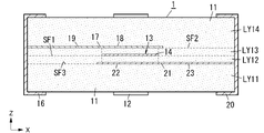
- FIG. 1 is a perspective perspective view of the laminated varistor 1 of the first embodiment
- FIG. 2 is a perspective view of the laminated varistor 1 from above
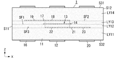
- FIG. 3 is a cross-sectional view of the laminated varistor 1.
- the laminated varistor 1 includes a sintered body 11, a first external electrode 12, a second external electrode 16, a third external electrode 20, a first internal electrode 13, a second internal electrode 17, and a third internal electrode. 21 and.
- the sintered body 11 excluding the external electrode of the laminated varistor 1 has, for example, a rectangular parallelepiped shape having a length of 1.6 mm, a width of 0.8 mm, and a height of 0.8 mm.
- the corners of the sintered body 11 may be chamfered as appropriate, and the sintered body 11 may be chamfered.
- the corners may be rounded.
- the X-axis direction parallel to the long side direction of the sintered body 11 is defined as the left-right direction
- the Y-axis direction is defined as the front-rear direction (depth direction)
- the Z-axis direction is defined as the vertical direction. ..
- the positive direction in the X-axis direction is defined as the right side
- the positive direction in the Y-axis direction is defined as the front side
- the positive direction in the Z-axis direction is defined as the upper side.
- these directions are examples, and are not intended to limit the directions when the laminated varistor 1 is used.
- the arrows indicating each direction in the drawing are shown only for the sake of explanation, and are not accompanied by an entity.
- the sintered body 11 has a first end surface S11 and a second end surface S12 facing each other in the first direction, and a first side surface S21 and a second side surface S22 facing each other in the second direction. Further, it has a first main surface S31 and a second main surface S32 facing each other in the third direction.
- the sintered body 11 has a laminated structure in which a plurality of layers LY11 to LY14 (see FIG. 3) are laminated in a third direction, and is formed in a rectangular parallelepiped shape having a long side in the first direction.
- the sintered body 11 is composed of a semiconductor ceramic component having non-linear resistance characteristics.
- the sintered body 11 may contain, for example, ZnO as a main component and at least one of Bi 2 O 3 , Co 2 O 3 , MnO 2 , and Sb 2 O 3 as a sub component, and Pr 6 O 11 may be contained. , Co 2 O 3 , CaCO 3 , and Cr 2 O 3 may be contained.
- ZnO is sintered and other subcomponents are precipitated at the grain boundaries thereof, and an internal electrode is formed between the layers. Then, the non-linear resistance characteristic is exhibited by the grain boundary barrier formed between the ZnO particles.
- the sintered body 11 is formed, for example, by laminating four layers LY11 to LY14 (see FIG. 3) containing ZnO as a main component and then sintering the layers.
- a first external electrode 12 is provided at the center of the side surface on the long side of the sintered body 11.
- the first external electrode 12 is electrically connected to the first internal electrode 13.
- the sintered body 11 is provided with two first external electrodes 12, one of the two first external electrodes 12 is provided on the first side surface S21, and the other of the two first external electrodes 12. Is provided on the second side surface S22.
- the two first external electrodes 12 are electrically connected via the first internal electrode 13.
- a second external electrode 16 and a third external electrode 20 are provided on both sides of the first external electrode 12.
- the second external electrode 16 and the third external electrode 20 are provided on both sides of each of the two first external electrodes 12. That is, the first side surface S21 is provided with the second external electrode 16 and the third external electrode 20 on both sides of the first external electrode 12, and the second side surface S22 is provided with the second outside on both sides of the first external electrode 12.
- the electrode 16 and the third external electrode 20 are provided.
- the sintered body 11 is provided with two second external electrodes 16, one of the two second external electrodes 16 is provided on the first side surface S21, and the other of the two second external electrodes 16 is provided. It is provided on the second side surface S22.
- the sintered body 11 is provided with two third external electrodes 20, one of the two third external electrodes 20 is provided on the first side surface S21, and the other of the two third external electrodes 20 is provided. It is provided on the second side surface S22.
- a second internal electrode 17 electrically connected to the second external electrode 16 and a third internal electrode 21 electrically connected to the third external electrode 20 are provided inside the sintered body 11, a second internal electrode 17 electrically connected to the second external electrode 16 and a third internal electrode 21 electrically connected to the third external electrode 20 are provided. ..
- the second external electrode 16 is electrically connected to the second internal electrode 17, and the third external electrode 20 is electrically connected to the third internal electrode 21. That is, the two second external electrodes 16 provided on the sintered body 11 are electrically connected via the second internal electrode 17, and the two third external electrodes 20 provided on the sintered body 11 are electrically connected to each other. It is electrically connected via the third internal electrode 21.
- the sintered body 11 is formed by laminating, for example, four layers LY11 to LY14 in the third direction (see FIG. 3).
- the first internal electrode 13 is provided by printing on, for example, the upper surface of the layer LY12 (hereinafter, also referred to as the first laminated surface SF1) among the four layers LY11 to LY14.
- the second internal electrode 17 is provided, for example, on the upper surface of the layer LY13 laminated on the upper side of the layer LY12 (hereinafter, also referred to as the second laminated surface SF2) by printing.
- the third internal electrode 21 is provided, for example, on the upper surface of the layer LY11 laminated on the lower side of the layer LY12 (hereinafter, also referred to as the third laminated surface SF3) by printing.
- the first internal electrode 13 is provided on the first laminated surface SF1 inside the sintered body 11.
- the second internal electrode 17 is provided inside the sintered body 11 on a second laminated surface SF2 different from the first laminated surface SF1.
- the third internal electrode 21 is provided inside the sintered body 11 on a third laminated surface SF3 different from the first laminated surface SF1 and the second laminated surface SF2.
- the first internal electrode 13 is arranged between the second internal electrode 17 and the third internal electrode 21.
- the first internal electrode 13 has a first facing portion 14 and a first drawing portion 15.
- the width of the first drawer portion 15 is narrower than that of the first facing portion 14.
- the first drawer portion 15 projects from the first facing portion 14 along the second direction.
- two first drawer portions 15 project from the first facing portion 14 toward the front side and the rear side.
- One of the two first drawers 15 is electrically connected to the first external electrode 12 provided on the first side surface S21, and the other of the two first drawers 15 is provided on the second side surface S22. It is electrically connected to the first external electrode 12.
- the second internal electrode 17 has a second facing portion 18 and a second lead-out portion 19.
- the width of the second drawer portion 19 is narrower than that of the second facing portion 18.
- the second drawer portion 19 projects from the second facing portion 18 along the first direction.
- the second drawer portion 19 has a first connecting portion 19B that connects between the two second external electrodes 16 and a second facing portion 18 along the first direction. It has a first protruding portion 19A that protrudes and is connected to the first connecting portion 19B.
- the first protruding portion 19A protrudes from the second facing portion 18, for example, to the left.
- the first connecting portion 19B projects from the left end portion of the first protruding portion 19A to the front side and the rear side, respectively, and connects between the two second external electrodes 16.
- the third internal electrode 21 has a third facing portion 22 and a third lead-out portion 23.
- the width of the third drawer portion 23 is narrower than that of the third facing portion 22.
- the third drawer portion 23 projects from the third facing portion 22 along the first direction. In the present embodiment, the third drawer portion 23 projects in the opposite direction to the second drawer portion 19, for example, to the right.
- the third lead-out portion 23 has a second connecting portion 23B that connects between the two third external electrodes 20, and a second connecting portion 23 that protrudes from the third facing portion 22 along the first direction. It has a second protruding portion 23A connected to the portion 23B.
- the second protruding portion 23A protrudes from the third facing portion 22, for example, to the right.
- the second connecting portion 23B projects from the right end portion of the second protruding portion 23A to the front side and the rear side, respectively, and connects between the two third external electrodes 20.
- the first internal electrode 13 is formed on the first laminated surface SF1
- the second internal electrode 17 is formed on the second laminated surface SF2
- the third internal electrode 21 is formed on the third laminated surface SF3.
- the 1 internal electrode 13, the 2nd internal electrode 17, and the 3rd internal electrode 21 are all arranged along the second direction.
- the length of the first facing portion 14 is longer than the length of the second facing portion 18 and the third facing portion 22. Further, in the second direction, the length of the first facing portion 14 is longer than the length of the second facing portion 18 and the third facing portion 22. Therefore, the area of the first facing portion 14 is larger than the area of the second facing portion 18 and the third facing portion 22. Since such a first facing portion 14 is arranged between the second facing portion 18 and the third facing portion 22, the stray capacitance generated between the second facing portion 18 and the third facing portion 22 is reduced. Therefore, crosstalk can be suppressed.
- the two first external electrodes 12, the two second external electrodes 16, and the two third external electrodes 20 have long sides when the sintered body 11 is viewed from the stacking direction. It is provided on both side surfaces (first side surface S21 and second side surface S22). In the first direction, since the first external electrode 12 exists between the second external electrode 16 and the third external electrode 20, the stray capacitance between the second external electrode 16 and the third external electrode 20 can be reduced. Further, the two first external electrodes 12, the two second external electrodes 16, and the two third external electrodes 20 are connected by the first drawer portion 15, the second drawer portion 19, and the third drawer portion 23, respectively. Has been done.
- the first external electrode 12, the second external electrode 16, and the third external electrode 20 can be formed at the same time, the process can be simplified, and the shape can be stably provided. It is possible to obtain a laminated varistor 1 having less variation in characteristics.
- the first internal electrode 13 is provided so as to be sandwiched between the second internal electrode 17 and the third internal electrode 21 in the stacking direction of the sintered body 11. That is, the first internal electrode 13 exists between the second internal electrode 17 and the third internal electrode 21 in the third direction. Specifically, the first facing portion 14 exists between the second internal electrode 17 and the third internal electrode 21. In other words, the second facing portion 18 and the third facing portion 22 face each other, and the first internal electrode 13 exists between the second facing portion 18 and the third facing portion 22. Therefore, the first facing portion 14 exists between the second facing portion 18 and the third facing portion 22.
- the varistor region is formed by the second facing portion 18 and the first facing portion 14 facing each other, and the first facing portion 14 and the third facing portion 22 facing each other.
- FIG. 5 is a schematic circuit diagram showing a usage example of the laminated varistor 1 of the present embodiment.
- the laminated varistor 1 of the present embodiment is composed of a first varistor 1A composed of a first external electrode 12 and a second external electrode 16, and a first external electrode 12 and a third external electrode 20. It has a second varistor 1B and the like.
- the circuit diagram of FIG. 5 shows a state in which the laminated varistor 1 is arranged in the vicinity of the communication IC 2 that communicates by the two-wire differential voltage transmission method.
- the land of the signal lines 3 and 4 and the land of the ground line 5 are connected to the communication IC 2.
- the pair of first external electrodes 12 on the first side surface S21 and the second side surface S22 are connected to the land of the ground line 5, respectively, and the pair of second external electrodes 16 on the first side surface S21 and the second side surface S22 are connected to each other.
- Each is connected to the land of the signal line 3
- the pair of third external electrodes 20 on the first side surface S21 and the second side surface S22 are connected to the land of the signal line 4, respectively.
- the first facing portion 14 is, for example, a rectangle of 0.46 mm ⁇ 0.20 mm
- the second facing portion 18 and the third facing portion 22 are, for example, a rectangle of 0.40 mm ⁇ 0.14 mm. It has become.
- the first facing portion 14 and the second facing portion 18 face each other at a distance of, for example, 0.035 mm.
- the first facing portion 14 and the third facing portion 22 face each other at a distance of, for example, 0.035 mm.
- the centers of each are at the same position when viewed from the stacking direction.
- the first facing portion 14 protrudes 0.03 mm from the second facing portion 18 and the third facing portion 22 and covers the entire circumference of the second facing portion 18 and the third facing portion 22. It is in a state of being. In other words, when viewed from the third direction, the first facing portion 14 covers the outer circumferences of the second facing portion 18 and the third facing portion 22. By doing so, it is possible to prevent stray capacitance from being generated between the second facing portion 18 and the third facing portion 22, and to suppress crosstalk. It should be noted that each of the above dimensions is an example and can be changed as appropriate.
- a second drawing portion 19 having a width of 0.1 mm extends and is connected to the second external electrode 16.
- a third drawer portion 23 having a width of 0.1 mm extends and is connected to the third external electrode 20.
- a first drawing portion 15 having a width of 0.1 mm extends and is connected to the first external electrode 12. Since the lead portion having a width narrower than that of the facing portion is connected to the external electrode in this way, the stray capacitance between the second external electrode 16 and the third external electrode 20 can be reduced, and crosstalk can be achieved. The impact can be minimized.
- the width of the second drawer portion 19 is 90% or less of the width of the second facing portion 18. Further, in the second direction, it is more desirable that the width of the second drawer portion 19 is 70% or less of the width of the second facing portion 18. Similarly, in the second direction, it is desirable that the width of the third drawer portion 23 is 90% or less of the width of the third facing portion 22. Further, in the second direction, it is more desirable that the width of the second drawer portion 19 is 70% or less of the width of the second facing portion 18. On the contrary, when the widths of the second drawer portion 19 and the third drawer portion 23 are larger than 90% of the widths of the second facing portion 18 and the third facing portion 22, respectively, the stray capacitance affecting the crosstalk becomes large.
- the width of the second drawer portion 19 is set to 90% or less of the width of the second facing portion 18 in the second direction.
- the stray capacitance generated in the first varistor 1A is reduced and the occurrence of crosstalk is suppressed. can.
- the width of the third drawer portion 23 is set to 90% or less of the width of the third facing portion 22 in the second direction, the stray capacitance generated in the second varistor 1B is reduced and the occurrence of crosstalk is suppressed. can.
- the absolute value of the difference between the stray capacitance of the first varistor 1A and the stray capacitance of the second varistor 1B can be reduced to suppress crosstalk.
- the width of the second drawer portion 19 is preferably 0.08 mm or more, and more preferably 0.1 mm or more.
- the width of the third drawer 23 is preferably 0.08 mm or more, and more preferably 0.1 mm or more.
- the width of the first drawer portion 15 is 90% or less of the width of the first facing portion 14. Further, it is more desirable that the width of the first drawer portion 15 is 70% or less of the width of the first facing portion 14 in the first direction.
- the width of the first drawer portion 15 is 0.08 mm or more, and more preferably 0.1 mm or more. This has the advantage that the shape of the first drawer portion 15 can be easily maintained.
- the size of the first facing portion 14 protruding from the outer periphery of the second facing portion 18 and the third facing portion 22 in the first direction is the length of the second facing portion 18 and the third facing portion 22. It is desirable that it is 7.5% or more and 15% or less with respect to the side. In other words, in the first direction, the length of the first facing portion 14 is preferably 107.5% or more and 115% or less of the length of the second facing portion 18 or the third facing portion 22.
- the amount of protrusion of the first facing portion 14 is smaller than 7.5% with respect to the long sides of the second facing portion 18 and the third facing portion 22, the crosstalk increases sharply, and when it becomes larger than 15%, it is manufactured.
- the length of the first facing portion 14 is more preferably 9% or more and 13.5% or less of the length of the second facing portion 18 or the third facing portion 22, and is more preferably crosstalk. Can be further reduced, and the deviation in manufacturing can be alleviated.
- the length of the first facing portion 14 is preferably 107.5% or more and 115% or less of the length of the second facing portion 18 or the third facing portion 22.
- the amount of protrusion of the first facing portion 14 is smaller than 7.5% with respect to the long sides of the second facing portion 18 and the third facing portion 22, the crosstalk increases sharply, and when it becomes larger than 15%, it is manufactured. This is because the above deviation cannot be alleviated and the capacity difference between the first varistor 1A and the second varistor 1B becomes large.
- the volume of the region sandwiched between the first facing portion 14 and the second facing portion 18 is preferably 5% or less of the volume of the entire sintered body 11 and is preferably 1% or less. It is desirable to do. When it is larger than 1%, the entire varistor region is in close proximity to the external electrode, so that the capacitance that affects crosstalk increases.
- the area of the first facing portion 14 is larger than the area of the second facing portion 18 or the third facing portion 22.
- the first to third internal electrodes 13, so that the area of the first facing portion 14 is larger than the area of the second facing portion 18 and larger than the area of the third facing portion 22. 17, 21 are formed.
- the first facing portion 14 of the first internal electrode 13 is the third facing portion 18 of the second internal electrode 17 and the third facing portion 22 of the third internal electrode 21 inside the sintered body 11, respectively. They are arranged at overlapping positions in the direction. That is, the first internal electrode 13 has a superposed region A1 (see FIG. 2) that overlaps with the second internal electrode 17 and the third internal electrode 21 in the third direction.
- the superimposed region A1 is a rectangular region whose longitudinal direction is the first direction.
- the length L1 of the superimposing region A1 in the first direction is longer than the length L2 of the superimposing region A1 in the second direction.
- the laminated varistor 1 of the present embodiment includes the first varistor 1A and the second varistor 1B
- the capacitances of the first varistor 1A and the second varistor 1B are 200 pF or less, respectively.
- the difference between the capacitance of the first varistor 1A and the capacitance of the second varistor 1B is preferably ⁇ 20% or more and + 20% or less of the capacitance of the first varistor 1A.
- FIG. 6 is a perspective perspective view of the laminated varistor 1 of the second embodiment
- FIG. 7 is an external perspective view of the laminated varistor 1 of the second embodiment.
- the second external electrode 16 and the third external electrode 20 are provided on both side surfaces which are long sides, whereas in the laminated varistor 1 of the second embodiment, the sintered body 11 is provided.
- the second external electrode 16 is provided on the first end surface S11
- the third external electrode 20 is provided on the second end surface S12 of the sintered body 11. Since the configurations of the first internal electrode 13, the second internal electrode 17, and the third internal electrode 21 are the same as those in the first embodiment, the common components are designated by the same reference numerals and the description thereof will be omitted. ..
- the first external electrode 12 is provided on a part of the first side surface S21 and a part of the second side surface S22.
- the second external electrode 16 is provided on at least a part of the first end surface S11.
- the second external electrode 16 is provided on the entire first end surface S11, from the first end surface S11 to a part of the first side surface S21 and the second side surface S22, and the first main surface S31 and the second main surface. It is provided over a part of S32.
- the third external electrode 20 is provided on at least a part of the second end surface S12.
- the third external electrode 20 is provided on the entire second end surface S12, from the second end surface S12 to a part of the first side surface S21 and the second side surface S22, and the first main surface S31 and the second main surface. It is provided over a part of S32.
- the second external electrode 16 is provided from the first end surface S11 to a part of the first side surface S21, the second side surface S22, the first main surface S31, and the second main surface S32. Therefore, the distance between the second external electrode 16 and the first external electrode 12 can be made wider than that of the laminated varistor 1 of the first embodiment, and the second external electrode 16 and the first external electrode 12 can be obtained. The floating capacity between can be reduced.
- the third external electrode 20 is provided from the second end surface S12 to a part of the first side surface S21, the second side surface S22, the first main surface S31, and the second main surface S32. Therefore, the distance between the third external electrode 20 and the first external electrode 12 can be made wider than that of the laminated varistor 1 of the first embodiment, and the third external electrode 20 and the first external electrode 12 can be obtained. The floating capacity between can be reduced.
- the second external electrode 16 and the third external electrode 20 are provided.
- the distance between 20 and 20 can be increased as compared with the laminated varistor 1 of the first embodiment, and the influence on the crosstalk can be further reduced.
- FIG. 8 is a perspective perspective view of the laminated varistor 1 of the third embodiment
- FIG. 9 is a perspective top view of the laminated varistor 1 of the third embodiment
- FIG. 10 is a cross-sectional view of the laminated varistor 1 of the third embodiment.
- the first facing portion 14 covers the outer periphery of the second facing portion 18 and the third facing portion 22, whereas in the third embodiment, it is shown in FIGS. 9 and 10.
- a part of the second facing portion 18 and the third facing portion 22 projects to the outside of the first facing portion 14. Since the components other than the first internal electrode 13, the second internal electrode 17, and the third internal electrode 21 have the same configuration as that of the laminated varistor 1 of the second embodiment, the components common to the second embodiment may be included. The same reference numerals are given, and the description thereof will be omitted.
- the second facing portion 18 is formed in a rectangular shape with the first direction as the longitudinal direction.
- the length of the second facing portion 18 in the first direction is longer than the length of the first facing portion 14 in the first direction, and the length of the second facing portion 18 in the second direction is the first of the first facing portions 14. Shorter than the length in two directions.
- the third facing portion 22 is formed in a rectangular shape with the first direction as the longitudinal direction.
- the length of the third facing portion 22 in the first direction is longer than the length of the first facing portion 14 in the first direction, and the length of the third facing portion 22 in the second direction is the length of the first facing portion 14. Shorter than the length in two directions.
- the first facing portion 14 and the second facing portion 18 face each other at a predetermined interval, and the first facing portion 14 and the third facing portion 22 face each other at a predetermined interval.
- the centers of the first facing portion 14, the second facing portion 18, and the third facing portion 22 are at the same position when viewed from the stacking direction, and the second facing portion 18 and the third facing portion 22 are viewed from the stacking direction. Almost overlap. Further, when viewed from the stacking direction, in the first direction, the right end and the left end of the second facing portion 18 protrude from the first facing portion 14, and the right end and the left end of the third facing portion 22 are the first facing portions. It sticks out of 14.
- the second facing portion 18 is covered with the first facing portion 14 except for the protruding portions at the right end and the left end.
- the third facing portion 22 is covered with the first facing portion 14 except for the protruding portions at the right end and the left end.
- the first internal electrode 13 is placed with respect to the second internal electrode 17 and the third internal electrode 21.
- the position may shift in the first direction.
- the capacitance generated between the first external electrode 12 and the second external electrode 16 There is a possibility that the capacitance difference with the capacitance generated between the first external electrode 12 and the third external electrode 20 becomes large.
- the second facing portion 18 and the third facing portion 22 are provided so as to protrude from both sides of the first facing portion 14 in the first direction, the second internal electrode 17 and the third are provided. Even when the position of the first internal electrode 13 is displaced in the first direction with respect to the internal electrode 21, the capacitance generated between the first external electrode 12 and the second external electrode 16 and the first external electrode 12 The capacitance difference with the capacitance generated between the third external electrode 20 and the third external electrode 20 can be reduced. Therefore, there is an advantage that crosstalk generated due to the capacitance difference between the first varistor 1A and the second varistor 1B can be suppressed.
- Table 1 below shows the relationship between the ratio of the horizontal dimension (length L1) to the vertical dimension (length L2) of the superposed region A1 and the capacitance difference caused by the variation in the dimensions.
- the dimensional variation is the dimensional variation between the internal electrodes or the dimensional variation between the internal electrode and the external electrode that occurs in each process such as printing, laminating, cutting, and forming the external electrode of the internal electrode. ..
- the capacitance difference is the absolute value of the difference between the stray capacitance generated between the first internal electrode 13 and the second internal electrode 17 and the stray capacitance generated between the first internal electrode 13 and the third internal electrode 21. Is. In Table 1, the capacity difference of Examples 1, 3 and 4 and Comparative Examples 1 and 2 is evaluated with the capacity difference of Example 2 as 1.
- the sintered body 11 has a rectangular shape having a length of 1.6 mm, a width of 0.8 mm, and a height of 0.8 mm
- the first facing portion 14 has a rectangular shape having a length of 0.44 mm and a width of 0.22 mm.
- the second facing portion 18 and the third facing portion 22 have a rectangular shape having a length of 0.54 mm and a width of 0.12 mm.
- the ratio of the length L1 of the superimposed region A1 in the first direction to the length L2 of the superimposed region A1 in the second direction is 1.3 or more and 7.5 or less.
- the difference in capacitance between the first varistor 1A and the second varistor 1B can be reduced to improve the communication quality.
- Table 2 below shows the relationship between the ratio of the area of the overlapping region A1 to the area of the first laminated surface SF1 of the sintered body 11 (area ratio) and the capacity difference generated by the variation in dimensions.
- the dimensional variation is the dimensional variation between the internal electrodes caused in each process such as printing, laminating, cutting, and forming the external electrode of the internal electrode, or the dimensional variation between the internal electrode and the external electrode. That is.
- the capacitance difference is the absolute value of the difference between the stray capacitance generated between the first internal electrode 13 and the second internal electrode 17 and the stray capacitance generated between the first internal electrode 13 and the third internal electrode 21. Is.
- the capacity difference of Examples 5 and 6 and Comparative Examples 3 and 4 is evaluated with the capacity difference of Example 2 as 1.
- the sintered body 11 has a rectangular shape having a length of 1.6 mm, a width of 0.8 mm, and a height of 0.8 mm
- the first facing portion 14 has a rectangular shape having a length of 0.44 mm and a width of 0.22 mm.
- the second facing portion 18 and the third facing portion 22 have a rectangular shape having a length of 0.54 mm and a width of 0.12 mm.
- the ratio of the area of the superimposed region A1 to the cross-sectional area of the sintered body 11 on the first laminated surface SF1 is 0.024 or more and 0.161 or less.
- the difference in capacitance between the first varistor 1A and the second varistor 1B can be reduced to improve the communication quality.
- the first internal electrode 13 overlaps with the second internal electrode 17 and the third internal electrode 21 in the third direction.
- the superimposed region A1 exists in the second region A3 other than the first region A2 on which the first external electrode 12, the second external electrode 16, and the third external electrode 20 are projected on the first laminated surface SF1. ing.
- the stray capacitance generated between the first external electrode 12, the second external electrode 16 and the third external electrode 20 can be reduced, and crosstalk can be suppressed.
- the superimposed region A1 is the first one on which the first external electrode 12, the second external electrode 16, and the third external electrode 20 are projected on the first laminated surface SF1, respectively. It exists in the second region A3 other than the region A2, and the occurrence of crosstalk can be suppressed.
- the first internal electrode 13, the second internal electrode 17, and the third internal electrode 21 of the third embodiment may be applied to the laminated varistor 1 of the first embodiment, which is the same as that of the laminated varistor 1 of the third embodiment. There are advantages.
- one layer each of the second internal electrode 17 and the first internal electrode 13 facing each other and the third internal electrode 21 and the first internal electrode 13 facing each other is one layer.
- they may face each other in multiple layers.
- the second internal electrode 17 and the first internal electrode 13 may face each other in multiple layers, or the third internal electrode 21 and the first internal electrode 13 may have multiple layers. It may be opposed to each other.
- the first external electrode 12, the second external electrode 16, and the third external electrode 20 are provided on each of the first side surface S21 and the second side surface S22.
- the external electrode 12, the second external electrode 16, and the third external electrode 20 may be provided on at least one of the first side surface S21 and the second side surface S22. That is, the first external electrode 12, the second external electrode 16, and the third external electrode 20 may be provided only on one of the first side surface S21 and the second side surface S22.
- the sintered body 11 is formed by laminating four layers LY11 to LY14, but the sintered body 11 is not limited to one having a four-layer laminated structure, and a plurality of layers are laminated. It suffices to have a structure.
- the laminated varistor 1 according to the present disclosure is industrially useful because it is possible to obtain a laminated varistor 1 with suppressed crosstalk by reducing the stray capacitance generated between the external electrodes.
Landscapes
- Engineering & Computer Science (AREA)
- Microelectronics & Electronic Packaging (AREA)
- Physics & Mathematics (AREA)
- Electromagnetism (AREA)
- Thermistors And Varistors (AREA)
Priority Applications (4)
| Application Number | Priority Date | Filing Date | Title |
|---|---|---|---|
| CN202411467804.2A CN119274903A (zh) | 2020-12-24 | 2021-12-17 | 多层压敏电阻 |
| US17/796,143 US12224090B2 (en) | 2020-12-24 | 2021-12-17 | Multilayer varistor |
| CN202180010816.0A CN115023774B (zh) | 2020-12-24 | 2021-12-17 | 多层压敏电阻 |
| JP2022571418A JP7843470B2 (ja) | 2020-12-24 | 2021-12-17 | 積層バリスタ |
Applications Claiming Priority (2)
| Application Number | Priority Date | Filing Date | Title |
|---|---|---|---|
| JP2020-214486 | 2020-12-24 | ||
| JP2020214486 | 2020-12-24 |
Publications (1)
| Publication Number | Publication Date |
|---|---|
| WO2022138515A1 true WO2022138515A1 (ja) | 2022-06-30 |
Family
ID=82157835
Family Applications (1)
| Application Number | Title | Priority Date | Filing Date |
|---|---|---|---|
| PCT/JP2021/046881 Ceased WO2022138515A1 (ja) | 2020-12-24 | 2021-12-17 | 積層バリスタ |
Country Status (4)
| Country | Link |
|---|---|
| US (1) | US12224090B2 (https=) |
| JP (1) | JP7843470B2 (https=) |
| CN (2) | CN115023774B (https=) |
| WO (1) | WO2022138515A1 (https=) |
Cited By (1)
| Publication number | Priority date | Publication date | Assignee | Title |
|---|---|---|---|---|
| WO2025198014A1 (ja) * | 2024-03-21 | 2025-09-25 | パナソニックIpマネジメント株式会社 | 積層セラミック部品 |
Families Citing this family (1)
| Publication number | Priority date | Publication date | Assignee | Title |
|---|---|---|---|---|
| JP7745231B2 (ja) * | 2021-02-24 | 2025-09-29 | パナソニックIpマネジメント株式会社 | 積層バリスタ |
Citations (4)
| Publication number | Priority date | Publication date | Assignee | Title |
|---|---|---|---|---|
| JPS5969902A (ja) * | 1982-10-15 | 1984-04-20 | 日本電気株式会社 | 三端子型積層バリスタ |
| JPH04125902A (ja) * | 1990-09-17 | 1992-04-27 | Nec Corp | 三端子積層チップバリスタ |
| JP2002305103A (ja) * | 2001-04-05 | 2002-10-18 | Matsushita Electric Ind Co Ltd | 多連形積層バリスタ |
| JP2020096075A (ja) * | 2018-12-12 | 2020-06-18 | Tdk株式会社 | チップバリスタ |
Family Cites Families (9)
| Publication number | Priority date | Publication date | Assignee | Title |
|---|---|---|---|---|
| JP2550846Y2 (ja) * | 1991-07-12 | 1997-10-15 | 株式会社村田製作所 | サージアブソーバ |
| JPH07235406A (ja) | 1994-02-25 | 1995-09-05 | Mitsubishi Materials Corp | チップ容量性バリスタ |
| JPH09205019A (ja) * | 1996-01-25 | 1997-08-05 | Murata Mfg Co Ltd | 複合機能素子及びその製造方法 |
| JP3900104B2 (ja) * | 2003-04-10 | 2007-04-04 | 松下電器産業株式会社 | 静電気対策部品 |
| DE102005012395A1 (de) * | 2005-03-17 | 2006-09-21 | Epcos Ag | Durchführungsfilter und elektrisches Mehrschicht-Bauelement |
| JP2007115931A (ja) * | 2005-10-21 | 2007-05-10 | Taiyo Yuden Co Ltd | バリスタ |
| JP4506701B2 (ja) * | 2006-03-27 | 2010-07-21 | Tdk株式会社 | 積層型バリスタアレイ |
| JP2014241452A (ja) * | 2014-08-13 | 2014-12-25 | 株式会社村田製作所 | 積層セラミック電子部品 |
| JP2017204547A (ja) * | 2016-05-11 | 2017-11-16 | パナソニックIpマネジメント株式会社 | 積層バリスタ |
-
2021
- 2021-12-17 JP JP2022571418A patent/JP7843470B2/ja active Active
- 2021-12-17 CN CN202180010816.0A patent/CN115023774B/zh active Active
- 2021-12-17 WO PCT/JP2021/046881 patent/WO2022138515A1/ja not_active Ceased
- 2021-12-17 CN CN202411467804.2A patent/CN119274903A/zh active Pending
- 2021-12-17 US US17/796,143 patent/US12224090B2/en active Active
Patent Citations (4)
| Publication number | Priority date | Publication date | Assignee | Title |
|---|---|---|---|---|
| JPS5969902A (ja) * | 1982-10-15 | 1984-04-20 | 日本電気株式会社 | 三端子型積層バリスタ |
| JPH04125902A (ja) * | 1990-09-17 | 1992-04-27 | Nec Corp | 三端子積層チップバリスタ |
| JP2002305103A (ja) * | 2001-04-05 | 2002-10-18 | Matsushita Electric Ind Co Ltd | 多連形積層バリスタ |
| JP2020096075A (ja) * | 2018-12-12 | 2020-06-18 | Tdk株式会社 | チップバリスタ |
Cited By (1)
| Publication number | Priority date | Publication date | Assignee | Title |
|---|---|---|---|---|
| WO2025198014A1 (ja) * | 2024-03-21 | 2025-09-25 | パナソニックIpマネジメント株式会社 | 積層セラミック部品 |
Also Published As
| Publication number | Publication date |
|---|---|
| JPWO2022138515A1 (https=) | 2022-06-30 |
| JP7843470B2 (ja) | 2026-04-10 |
| US12224090B2 (en) | 2025-02-11 |
| CN119274903A (zh) | 2025-01-07 |
| US20230079197A1 (en) | 2023-03-16 |
| CN115023774A (zh) | 2022-09-06 |
| CN115023774B (zh) | 2025-02-18 |
Similar Documents
| Publication | Publication Date | Title |
|---|---|---|
| CN100533615C (zh) | 层叠电容器 | |
| CN101310348B (zh) | 叠层电容器 | |
| WO2022138515A1 (ja) | 積層バリスタ | |
| KR101020528B1 (ko) | 적층 콘덴서 | |
| JP2004516676A (ja) | 電気的な多層半導体および該素子を備えている障害防止回路 | |
| KR20090088336A (ko) | 적층 콘덴서 | |
| JP2014183241A (ja) | 貫通型コンデンサ | |
| JP2005044871A (ja) | 3端子貫通型コンデンサ | |
| JP7611475B2 (ja) | 積層バリスタ | |
| JP2023095602A (ja) | 積層バリスタ及び製造方法 | |
| CN116724364A (zh) | 变阻器部件 | |
| JP7555038B2 (ja) | 積層バリスタ | |
| JP4507566B2 (ja) | 積層コンデンサ | |
| JP7833707B2 (ja) | 積層バリスタ | |
| JP7745231B2 (ja) | 積層バリスタ | |
| JP2024051994A (ja) | 電子部品 | |
| JP4508259B2 (ja) | 積層コンデンサ | |
| JP3727542B2 (ja) | 積層貫通型コンデンサ | |
| JP2017092406A (ja) | 電子部品の実装用基板及び実装構造 | |
| JP4508258B2 (ja) | 積層コンデンサ | |
| JP2024078110A (ja) | 積層バリスタ | |
| CN117894545A (zh) | 层叠线圈部件 | |
| JP2011223136A (ja) | 電子部品 | |
| JP2015153800A (ja) | 電子部品及び電子部品の実装構造体 |
Legal Events
| Date | Code | Title | Description |
|---|---|---|---|
| 121 | Ep: the epo has been informed by wipo that ep was designated in this application |
Ref document number: 21910660 Country of ref document: EP Kind code of ref document: A1 |
|
| ENP | Entry into the national phase |
Ref document number: 2022571418 Country of ref document: JP Kind code of ref document: A |
|
| NENP | Non-entry into the national phase |
Ref country code: DE |
|
| 122 | Ep: pct application non-entry in european phase |
Ref document number: 21910660 Country of ref document: EP Kind code of ref document: A1 |
|
| WWG | Wipo information: grant in national office |
Ref document number: 202180010816.0 Country of ref document: CN |