WO2022130588A1 - 半導体装置および半導体装置の製造方法 - Google Patents
半導体装置および半導体装置の製造方法 Download PDFInfo
- Publication number
- WO2022130588A1 WO2022130588A1 PCT/JP2020/047262 JP2020047262W WO2022130588A1 WO 2022130588 A1 WO2022130588 A1 WO 2022130588A1 JP 2020047262 W JP2020047262 W JP 2020047262W WO 2022130588 A1 WO2022130588 A1 WO 2022130588A1
- Authority
- WO
- WIPO (PCT)
- Prior art keywords
- nut
- semiconductor device
- lead frame
- semiconductor chip
- substrate
- Prior art date
- Legal status (The legal status is an assumption and is not a legal conclusion. Google has not performed a legal analysis and makes no representation as to the accuracy of the status listed.)
- Ceased
Links
Images





Classifications
-
- H—ELECTRICITY
- H10—SEMICONDUCTOR DEVICES; ELECTRIC SOLID-STATE DEVICES NOT OTHERWISE PROVIDED FOR
- H10W—GENERIC PACKAGES, INTERCONNECTIONS, CONNECTORS OR OTHER CONSTRUCTIONAL DETAILS OF DEVICES COVERED BY CLASS H10
- H10W40/00—Arrangements for thermal protection or thermal control
- H10W40/60—Securing means for detachable heating or cooling arrangements, e.g. clamps
- H10W40/611—Bolts or screws
-
- H—ELECTRICITY
- H10—SEMICONDUCTOR DEVICES; ELECTRIC SOLID-STATE DEVICES NOT OTHERWISE PROVIDED FOR
- H10W—GENERIC PACKAGES, INTERCONNECTIONS, CONNECTORS OR OTHER CONSTRUCTIONAL DETAILS OF DEVICES COVERED BY CLASS H10
- H10W90/00—Package configurations
- H10W90/701—Package configurations characterised by the relative positions of pads or connectors relative to package parts
-
- H—ELECTRICITY
- H10—SEMICONDUCTOR DEVICES; ELECTRIC SOLID-STATE DEVICES NOT OTHERWISE PROVIDED FOR
- H10W—GENERIC PACKAGES, INTERCONNECTIONS, CONNECTORS OR OTHER CONSTRUCTIONAL DETAILS OF DEVICES COVERED BY CLASS H10
- H10W40/00—Arrangements for thermal protection or thermal control
- H10W40/10—Arrangements for heating
-
- H—ELECTRICITY
- H10—SEMICONDUCTOR DEVICES; ELECTRIC SOLID-STATE DEVICES NOT OTHERWISE PROVIDED FOR
- H10W—GENERIC PACKAGES, INTERCONNECTIONS, CONNECTORS OR OTHER CONSTRUCTIONAL DETAILS OF DEVICES COVERED BY CLASS H10
- H10W72/00—Interconnections or connectors in packages
- H10W72/071—Connecting or disconnecting
-
- H—ELECTRICITY
- H10—SEMICONDUCTOR DEVICES; ELECTRIC SOLID-STATE DEVICES NOT OTHERWISE PROVIDED FOR
- H10W—GENERIC PACKAGES, INTERCONNECTIONS, CONNECTORS OR OTHER CONSTRUCTIONAL DETAILS OF DEVICES COVERED BY CLASS H10
- H10W90/00—Package configurations
-
- H—ELECTRICITY
- H10—SEMICONDUCTOR DEVICES; ELECTRIC SOLID-STATE DEVICES NOT OTHERWISE PROVIDED FOR
- H10W—GENERIC PACKAGES, INTERCONNECTIONS, CONNECTORS OR OTHER CONSTRUCTIONAL DETAILS OF DEVICES COVERED BY CLASS H10
- H10W40/00—Arrangements for thermal protection or thermal control
- H10W40/20—Arrangements for cooling
- H10W40/25—Arrangements for cooling characterised by their materials
- H10W40/255—Arrangements for cooling characterised by their materials having a laminate or multilayered structure, e.g. direct bond copper [DBC] ceramic substrates
-
- H—ELECTRICITY
- H10—SEMICONDUCTOR DEVICES; ELECTRIC SOLID-STATE DEVICES NOT OTHERWISE PROVIDED FOR
- H10W—GENERIC PACKAGES, INTERCONNECTIONS, CONNECTORS OR OTHER CONSTRUCTIONAL DETAILS OF DEVICES COVERED BY CLASS H10
- H10W72/00—Interconnections or connectors in packages
- H10W72/071—Connecting or disconnecting
- H10W72/072—Connecting or disconnecting of bump connectors
- H10W72/07231—Techniques
- H10W72/07236—Soldering or alloying
-
- H—ELECTRICITY
- H10—SEMICONDUCTOR DEVICES; ELECTRIC SOLID-STATE DEVICES NOT OTHERWISE PROVIDED FOR
- H10W—GENERIC PACKAGES, INTERCONNECTIONS, CONNECTORS OR OTHER CONSTRUCTIONAL DETAILS OF DEVICES COVERED BY CLASS H10
- H10W90/00—Package configurations
- H10W90/701—Package configurations characterised by the relative positions of pads or connectors relative to package parts
- H10W90/761—Package configurations characterised by the relative positions of pads or connectors relative to package parts of strap connectors
- H10W90/763—Package configurations characterised by the relative positions of pads or connectors relative to package parts of strap connectors between laterally-adjacent chips
-
- H—ELECTRICITY
- H10—SEMICONDUCTOR DEVICES; ELECTRIC SOLID-STATE DEVICES NOT OTHERWISE PROVIDED FOR
- H10W—GENERIC PACKAGES, INTERCONNECTIONS, CONNECTORS OR OTHER CONSTRUCTIONAL DETAILS OF DEVICES COVERED BY CLASS H10
- H10W90/00—Package configurations
- H10W90/811—Multiple chips on leadframes
Definitions
- This disclosure relates to a semiconductor device and a method for manufacturing the semiconductor device.
- Patent Document 1 discloses a method for manufacturing a power semiconductor device.
- an insulating layer and a metal circuit layer are adhered on a metal substrate, a heat radiating plate is placed on the upper surface of the metal circuit layer via a solder sheet, and a silicon semiconductor chip is placed on the upper surface of the heat radiating plate via the solder sheet.
- a terminal portion on one side of the lead frame is arranged on the upper surface of the silicon semiconductor chip via a solder sheet. All of these are heated to melt all the solder sheets.
- the metal circuit layer and the heat sink, the heat sink and the silicon semiconductor chip, and the silicon semiconductor chip and the one-side terminal portion of the lead frame are collectively joined.
- solder joining process as in Patent Document 1, it is conceivable that the solder is heated from the substrate side and melts. In this case, it may take time to melt the solder.
- An object of the present disclosure is to obtain a semiconductor device capable of melting solder in a short time and a method for manufacturing the semiconductor device.
- the semiconductor device includes a substrate, a semiconductor chip provided on the substrate, a nut, and a lead frame provided on the semiconductor chip and the nut and screwed to the nut.
- a nut box having an opening formed at the bottom for accommodating the nut and exposing the nut downward, and at least a solder provided between the semiconductor chip and the substrate or the lead frame. ..
- the method for manufacturing a semiconductor device includes a substrate, a semiconductor chip provided on the substrate, a nut, a semiconductor chip, a lead frame provided on the nut, and the nut.
- a semiconductor device comprising a nut box with an opening formed at the bottom to accommodate and expose the nut downward, and at least solder provided between the semiconductor chip and the substrate or lead frame. It is mounted on a lower jig having a convex portion on the upper surface, the convex portion is brought into contact with the nut through the opening, and the lower jig is heated with the convex portion in contact with the nut.
- the semiconductor chip is bonded to the substrate or the lead frame with the solder.
- the method for manufacturing a semiconductor device includes a substrate, a semiconductor chip provided on the substrate, a lead frame provided on the semiconductor chip, and at least the semiconductor chip and the substrate or the substrate.
- a semiconductor device including a solder provided between the lead frame and a case surrounding the semiconductor chip is mounted on a lower jig having a convex portion formed of metal on the upper surface thereof, and the convex portion is mounted on the lower jig. Is in contact with the lead frame, the lower jig is heated in a state where the convex portion is in contact with the lead frame, and the semiconductor chip and the substrate or the lead frame are joined with the solder.
- heat can be transferred to the solder via a lead frame. Therefore, the solder can be melted in a short time.
- FIG. It is sectional drawing of the semiconductor device which concerns on Embodiment 1.
- FIG. It is a flowchart which shows the manufacturing method of the semiconductor device which concerns on Embodiment 1. It is sectional drawing of the semiconductor device which concerns on a comparative example. It is sectional drawing of the semiconductor device which concerns on Embodiment 2. FIG. It is sectional drawing of the semiconductor device which concerns on Embodiment 3. FIG. It is sectional drawing of the semiconductor device which concerns on Embodiment 4. FIG. It is sectional drawing of the semiconductor device which concerns on Embodiment 5.
- FIG. 1 is a cross-sectional view of the semiconductor device 100 according to the first embodiment.
- the semiconductor device 100 has a DLB (Direct Lead Bonding) structure in which the lead frame 8 is directly soldered to the semiconductor chip 10.
- the semiconductor device 100 includes a base plate 2 and an insulating circuit board 4 bonded to the central portion of the upper surface of the base plate 2 with solder 3.
- the case 5 is fixed to the outer peripheral portion of the upper surface of the base plate 2 with an adhesive or the like.
- the base plate 2 is made of, for example, Cu, Al or AlSiC.
- the insulating circuit board 4 has an insulating substrate 6 and a circuit pattern 7 provided on the upper surface and the back surface of the insulating substrate 6.
- the circuit pattern 7 provided on the back surface of the insulating substrate 6 is fixed to the base plate 2 via the solder 3.
- the circuit pattern 7 provided on the upper surface of the insulating substrate 6 constitutes an electric circuit. Therefore, the circuit pattern 7 provided on the upper surface of the insulating substrate 6 has a lower coverage ratio on the insulating substrate 6 than the circuit pattern 7 provided on the back surface.
- the insulating substrate 6 is formed of, for example, Al2O3, AlN or Si3N4.
- the circuit pattern 7 is formed of, for example, Al or Cu.
- a plurality of semiconductor chips 10 are provided on the insulating circuit board 4.
- the back surfaces of the plurality of semiconductor chips 10 are fixed to the circuit pattern 7 provided on the upper surface of the insulating substrate 6 via the solder 9.
- the solder 9 is formed of, for example, paste solder or plate solder.
- the semiconductor chip 10 is formed of, for example, Si.
- the semiconductor chip 10 may be formed of a wide bandgap semiconductor. Wide bandgap semiconductors are, for example, silicon carbide, gallium nitride based materials or diamond.
- a lead frame 8 is provided on the plurality of semiconductor chips 10 and the nut 12 described later.
- the lead frame 8 is bonded to the upper surfaces of a plurality of semiconductor chips 10 via solder 11.
- the solder 11 is formed of, for example, paste solder or plate solder.
- the lead frame 8 is formed of, for example, Cu or Al.
- the lead frame 8 is fixed to the case 5.
- the case 5 surrounds the insulating circuit board 4 and the plurality of semiconductor chips 10.
- Case 5 is formed of, for example, PPS (Poly Phenylene Sulfide).
- a screw hole 12a is formed in the nut 12.
- the screw hole 12a overlaps with the through hole 8a formed in the lead frame 8 in a plan view.
- the nut 12 and the lead frame 8 are screwed with the screw 20 through the through hole 8a and the screw hole 12a.
- the nut 12 is made of, for example, aluminum, stainless steel or titanium.
- the nut box 13 stores the nut 12.
- the nut box 13 is open on the side where the lead frame 8 is provided.
- the nut 12 is in contact with the lead frame 8 while being housed in the nut box 13.
- the nut box 13 has an opening 13a formed at the bottom thereof to expose the nut 12 downward.
- the nut box 13 is provided outside the area of the case 5 for accommodating the semiconductor chip 10.
- the nut box 13 is fixed to the case 5.
- the nut box 13 may be a part of the case 5.
- the nut box 13 is formed of, for example, PPS.
- the lower jig 50 is used in the manufacturing process of the semiconductor device 100.
- the lower jig 50 has a convex portion 51 on the upper surface.
- the lower jig 50 is installed so as to come into contact with the base plate 2.
- the convex portion 51 is installed so as to come into contact with the nut 12 through the opening 13a.
- the lower jig 50 and the convex portion 51 are formed of a metal such as stainless steel.
- FIG. 2 is a flowchart showing a manufacturing method of the semiconductor device 100 according to the first embodiment.
- step S1 the base plate 2, the insulating circuit board 4, the semiconductor chip 10, the solder 3, 9, 11, the lead frame 8, the case 5, the nut 12, and the nut box 13 are mounted. Place in position. That is, the insulating circuit board 4 is arranged on the base plate 2 via the solder 3, and the semiconductor chip 10 is arranged on the insulating circuit board 4 via the solder 9. Further, the nut 12 is stored in the nut box 13. Further, the lead frame 8 is arranged on the semiconductor chip 10 via the solder 11. Further, the case 5 is arranged on the base plate 2. The end of the lead frame 8 is arranged on the nut 12.
- step S2 the semiconductor device 100 is placed on the lower jig 50.
- the convex portion 51 comes into contact with the nut 12 through the opening 13a of the nut box 13.
- step S3 the lower jig 50 is heated with the convex portion 51 in contact with the nut 12.
- the solders 3, 9 and 11 are heated via the base plate 2.
- the solders 3, 9 and 11 are heated via the nut 12 and the lead frame 8.
- the solders 3, 9 and 11 are melted. Therefore, the base plate 2 and the insulating circuit board 4, the semiconductor chip 10 and the insulating circuit board 4, the semiconductor chip 10 and the lead frame 8 are joined by solders 3, 9, and 11.
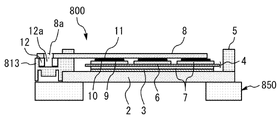
- FIG. 3 is a cross-sectional view of the semiconductor device 800 according to the comparative example.
- the semiconductor device 800 according to the comparative example is different from the semiconductor device 100 in that an opening is not formed at the bottom of the nut box 813.
- the semiconductor device 800 according to the comparative example when the lower jig 850 is heated, the solders 3, 9, and 11 are heated and melted through the base plate 2. At this time, it may take time to melt the solders 3, 9, and 11.
- heat can be transferred to the solders 3, 9, and 11 via the lead frame 8 by bringing the convex portion 51 of the lower jig 50 into contact with the nut 12. Therefore, the solders 3, 9 and 11 can be melted in a short time. This can improve the tact of the solder joining process.
- the solders 3, 9 and 11 can be reliably melted. Therefore, the reliability of the semiconductor device 100 can be improved.
- the convex portion 51 may have a higher thermal conductivity than the portion of the lower jig 50 other than the convex portion 51.
- the convex portion 51 is formed of, for example, Cu.
- step S3 the lower jig 50 may be heated while the lead frame 8 is pressed toward the convex portion 51. Pressurization is performed using, for example, a plunger. As a result, the contact thermal resistance between the lower jig 50 and the lead frame 8 can be reduced. Therefore, heat is easily transferred to the solders 3, 9, and 11.
- the configuration of the semiconductor device 100 is not limited to that shown in FIG. Although three semiconductor chips 10 are shown in FIG. 1, the number of semiconductor chips 10 provided in the semiconductor device 100 may be one or more. Further, the case 5 may be fixed to the insulating circuit board 4. Further, the solder may be provided at least between the semiconductor chip 10 and the insulating circuit board 4 or the lead frame 8.
- FIG. 4 is a cross-sectional view of the semiconductor device 200 according to the second embodiment.
- the structure of the lead frame 208 of the semiconductor device 200 is different from that of the semiconductor device 100. Other configurations are the same as those of the first embodiment.
- the lead frame 208 has a main body portion 208a and an external connection terminal portion 208b.
- the main body portion 208a is provided directly above the semiconductor chip 10.
- the external connection terminal portion 208b is joined to the main body portion 208a with solder 216 and is provided directly above the nut 12.
- the main body portion 208a and the external connection terminal portion 208b are formed of, for example, Cu or Al.
- the external connection terminal portion 208b is fixed by the case 5.
- heat can be transferred from the lower jig 50 to the solder 216 via the nut 12 and the external connection terminal portion 208b. Therefore, even when the lead frame 208 has a solder joint, the solder 216 can be melted in a short time.
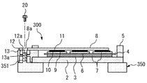
- FIG. 5 is a cross-sectional view of the semiconductor device 300 according to the third embodiment.
- the convex portion 351 of the lower jig 350 is inserted into the screw hole 12a of the nut 12.
- the convex portion 351 is threaded and screwed to the nut 12.
- the lead frame 8 and the nut 12 are screwed together with the screws 20.
- the lower jig 350 is heated with the convex portion 351 and the nut 12 and the lead frame 8 and the nut 12 screwed together.
- the lower jig 350 may be heated with only one of the protrusion 351 and the nut 12 or the nut 12 and the lead frame 8 screwed.
- FIG. 6 is a cross-sectional view of the semiconductor device 400 according to the fourth embodiment.
- the semiconductor device 400 differs from the semiconductor device 100 in that fins 417 are provided under the insulating circuit board 4. Other configurations are the same as those of the first embodiment.
- the fin 417 is provided on the back surface of the base plate 2.
- the fin 417 is, for example, a pin fin. Thereby, the cooling performance of the semiconductor device 400 can be improved.
- the fin 417 may be a part of the base plate 2 or may be a separate part from the base plate 2.
- FIG. 7 is a cross-sectional view of the semiconductor device 500 according to the fifth embodiment.
- the semiconductor device 500 is different from the semiconductor device 100 in that the nut 12 and the nut box 13 are not provided.
- Other configurations are the same as those of the first embodiment.
- the insulating circuit board 4 is placed on the base plate 2 via the solder 3, and the semiconductor chip 10 is placed on the insulating circuit board 4 via the solder 9. Further, the lead frame 8 is arranged on the semiconductor chip 10 via the solder 11. Further, the case 5 is arranged on the base plate 2.
- the semiconductor device 500 is mounted on the lower jig 50, and the convex portion 51 is brought into contact with the lead frame 8.
- the lower jig 50 is heated with the convex portion 51 in contact with the lead frame 8.
- the convex portion 51 of the lower jig 50 is formed of metal.
- the solders 3, 9 and 11 are heated via the base plate 2.
- the solders 3, 9 and 11 are heated via the lead frame 8.
- the solders 3, 9 and 11 are melted. Therefore, the base plate 2 and the insulating circuit board 4, the semiconductor chip 10 and the insulating circuit board 4, the semiconductor chip 10 and the lead frame 8 are joined by solders 3, 9, and 11.
Landscapes
- Cooling Or The Like Of Semiconductors Or Solid State Devices (AREA)
Abstract
Description
図1は、実施の形態1に係る半導体装置100の断面図である。半導体装置100は、リードフレーム8が半導体チップ10に直接はんだ接合されたDLB(Direct Lead Bonding)構造を有する。半導体装置100は、ベース板2と、ベース板2の上面のうち中央部にはんだ3で接合された絶縁回路基板4を備える。ベース板2の上面のうち外周部には、接着材等によりケース5が固定される。ベース板2は例えばCu、AlまたはAlSiCで形成されている。
図4は、実施の形態2に係る半導体装置200の断面図である。半導体装置200はリードフレーム208の構成が半導体装置100と異なる。他の構成は、実施の形態1の構成と同様である。リードフレーム208は、本体部208aと外部接続端子部208bを有する。本体部208aは、半導体チップ10の直上に設けられる。外部接続端子部208bは、本体部208aにはんだ216で接合され、ナット12の直上に設けられる。本体部208a、外部接続端子部208bは例えばCuまたはAlで形成される。外部接続端子部208bはケース5により固定される。
図5は、実施の形態3に係る半導体装置300の断面図である。半導体装置300の製造工程において、ナット12のネジ穴12aには、下治具350の凸部351が挿入される。凸部351はネジ切りされ、ナット12とネジ止めされる。また、リードフレーム8とナット12はネジ20でネジ止めされる。凸部351とナット12およびリードフレーム8とナット12がそれぞれネジ止めされた状態で、下治具350は加熱される。
図6は、実施の形態4に係る半導体装置400の断面図である。半導体装置400は、絶縁回路基板4の下にフィン417が設けられる点が、半導体装置100と異なる。他の構成は、実施の形態1の構成と同様である。フィン417は、ベース板2の裏面に設けられる。フィン417は、例えばピンフィンである。これにより、半導体装置400の冷却性能を向上させることができる。フィン417は、ベース板2の一部であっても良く、ベース板2とは別部品であっても良い。
図7は、実施の形態5に係る半導体装置500の断面図である。半導体装置500は、ナット12およびナットボックス13が設けられない点が、半導体装置100と異なる。他の構成は、実施の形態1の構成と同様である。
Claims (12)
- 基板と、
前記基板の上に設けられた半導体チップと、
ナットと、
前記半導体チップと前記ナットの上に設けられ、前記ナットとネジ止めされるリードフレームと、
前記ナットを収納し、下方に向かって前記ナットを露出させる開口が底部に形成されたナットボックスと、
少なくとも前記半導体チップと前記基板または前記リードフレームとの間に設けられたはんだと、
を備えることを特徴とする半導体装置。 - 前記リードフレームと前記ナットは接触することを特徴とする請求項1に記載の半導体装置。
- 前記半導体チップを囲むケースを備え、
前記ナットボックスは前記ケースに設けられることを特徴とする請求項1または2に記載の半導体装置。 - 前記リードフレームは、前記半導体チップの直上に設けられた本体部と、前記本体部にはんだで接合され前記ナットの直上に設けられた外部接続端子部と、を有することを特徴とする請求項1から3の何れか1項に記載の半導体装置。
- 前記基板の下に設けられたフィンを備えることを特徴とする請求項1から4の何れか1項に記載の半導体装置。
- 前記半導体チップはワイドバンドギャップ半導体によって形成されていることを特徴とする請求項1から5の何れか1項に記載の半導体装置。
- 前記ワイドバンドギャップ半導体は、炭化珪素、窒化ガリウム系材料またはダイヤモンドであることを特徴とする請求項6に記載の半導体装置。
- 基板と、前記基板の上に設けられた半導体チップと、ナットと、前記半導体チップと前記ナットの上に設けられたリードフレームと、前記ナットを収納し下方に向かって前記ナットを露出させる開口が底部に形成されたナットボックスと、少なくとも前記半導体チップと前記基板または前記リードフレームとの間に設けられたはんだと、を備えた半導体装置を、上面に凸部を有する下治具の上に搭載し、前記開口を介して前記凸部を前記ナットと接触させ、
前記凸部を前記ナットと接触させた状態で前記下治具を加熱し、前記半導体チップと前記基板または前記リードフレームを前記はんだで接合することを特徴とする半導体装置の製造方法。 - 基板と、前記基板の上に設けられた半導体チップと、前記半導体チップの上に設けられたリードフレームと、少なくとも前記半導体チップと前記基板または前記リードフレームとの間に設けられたはんだと、前記半導体チップを囲むケースと、を備えた半導体装置を、上面に金属から形成された凸部を有する下治具の上に搭載し、前記凸部を前記リードフレームと接触させ、
前記凸部を前記リードフレームと接触させた状態で前記下治具を加熱し、前記半導体チップと前記基板または前記リードフレームを前記はんだで接合することを特徴とする半導体装置の製造方法。 - 前記凸部は、前記下治具のうち前記凸部以外の部分よりも熱伝導率が高いことを特徴とする請求項8または9に記載の半導体装置の製造方法。
- 前記リードフレームを前記凸部に向かって押さえつけた状態で、前記下治具を加熱することを特徴とする請求項8から10の何れか1項に記載の半導体装置の製造方法。
- 前記凸部はネジ切りされ、前記ナットとネジ止めされることを特徴とする請求項8に記載の半導体装置の製造方法。
Priority Applications (5)
| Application Number | Priority Date | Filing Date | Title |
|---|---|---|---|
| US18/004,429 US20230298984A1 (en) | 2020-12-17 | 2020-12-17 | Semiconductor device and method for manufacturing semiconductor device |
| JP2022569636A JP7487798B2 (ja) | 2020-12-17 | 2020-12-17 | 半導体装置および半導体装置の製造方法 |
| DE112020007850.7T DE112020007850T5 (de) | 2020-12-17 | 2020-12-17 | Halbleitervorrichtung und Verfahren zur Herstellung der Halbleitervorrichtung |
| PCT/JP2020/047262 WO2022130588A1 (ja) | 2020-12-17 | 2020-12-17 | 半導体装置および半導体装置の製造方法 |
| CN202080107864.7A CN116601769B (zh) | 2020-12-17 | 2020-12-17 | 半导体装置以及半导体装置的制造方法 |
Applications Claiming Priority (1)
| Application Number | Priority Date | Filing Date | Title |
|---|---|---|---|
| PCT/JP2020/047262 WO2022130588A1 (ja) | 2020-12-17 | 2020-12-17 | 半導体装置および半導体装置の製造方法 |
Publications (1)
| Publication Number | Publication Date |
|---|---|
| WO2022130588A1 true WO2022130588A1 (ja) | 2022-06-23 |
Family
ID=82057471
Family Applications (1)
| Application Number | Title | Priority Date | Filing Date |
|---|---|---|---|
| PCT/JP2020/047262 Ceased WO2022130588A1 (ja) | 2020-12-17 | 2020-12-17 | 半導体装置および半導体装置の製造方法 |
Country Status (5)
| Country | Link |
|---|---|
| US (1) | US20230298984A1 (ja) |
| JP (1) | JP7487798B2 (ja) |
| CN (1) | CN116601769B (ja) |
| DE (1) | DE112020007850T5 (ja) |
| WO (1) | WO2022130588A1 (ja) |
Citations (3)
| Publication number | Priority date | Publication date | Assignee | Title |
|---|---|---|---|---|
| JP2003264265A (ja) * | 2002-03-08 | 2003-09-19 | Mitsubishi Electric Corp | 電力用半導体装置 |
| WO2015004990A1 (ja) * | 2013-07-10 | 2015-01-15 | 日立オートモティブシステムズ株式会社 | 電力用半導体モジュール |
| JP2019220648A (ja) * | 2018-06-22 | 2019-12-26 | 三菱電機株式会社 | パワーモジュール、電力変換装置、及びパワーモジュールの製造方法 |
Family Cites Families (9)
| Publication number | Priority date | Publication date | Assignee | Title |
|---|---|---|---|---|
| JP3063733B2 (ja) * | 1998-04-22 | 2000-07-12 | 日本電気株式会社 | 半導体パッケージ |
| JP2007157863A (ja) | 2005-12-02 | 2007-06-21 | Hitachi Ltd | パワー半導体装置及びその製造方法 |
| JP4907178B2 (ja) * | 2006-01-26 | 2012-03-28 | パナソニック株式会社 | 半導体装置およびそれを備えた電子機器 |
| JP5098772B2 (ja) * | 2007-06-29 | 2012-12-12 | ダイキン工業株式会社 | 電装品ユニット |
| EP2725609B1 (en) * | 2011-06-27 | 2019-11-13 | Rohm Co., Ltd. | Semiconductor module |
| JP6208262B2 (ja) * | 2014-01-09 | 2017-10-04 | 日立オートモティブシステムズ株式会社 | パワー半導体装置の製造方法、パワー半導体装置並びにそれを用いた電力変換装置 |
| JP6719585B2 (ja) * | 2016-11-29 | 2020-07-08 | 三菱電機株式会社 | 半導体装置、制御装置および半導体装置の製造方法 |
| JP7735655B2 (ja) * | 2020-10-15 | 2025-09-09 | 富士電機株式会社 | 半導体装置 |
| US11664434B2 (en) * | 2020-11-13 | 2023-05-30 | Wolfspeed, Inc. | Semiconductor power devices having multiple gate trenches and methods of forming such devices |
-
2020
- 2020-12-17 DE DE112020007850.7T patent/DE112020007850T5/de active Pending
- 2020-12-17 WO PCT/JP2020/047262 patent/WO2022130588A1/ja not_active Ceased
- 2020-12-17 US US18/004,429 patent/US20230298984A1/en active Pending
- 2020-12-17 CN CN202080107864.7A patent/CN116601769B/zh active Active
- 2020-12-17 JP JP2022569636A patent/JP7487798B2/ja active Active
Patent Citations (3)
| Publication number | Priority date | Publication date | Assignee | Title |
|---|---|---|---|---|
| JP2003264265A (ja) * | 2002-03-08 | 2003-09-19 | Mitsubishi Electric Corp | 電力用半導体装置 |
| WO2015004990A1 (ja) * | 2013-07-10 | 2015-01-15 | 日立オートモティブシステムズ株式会社 | 電力用半導体モジュール |
| JP2019220648A (ja) * | 2018-06-22 | 2019-12-26 | 三菱電機株式会社 | パワーモジュール、電力変換装置、及びパワーモジュールの製造方法 |
Also Published As
| Publication number | Publication date |
|---|---|
| JPWO2022130588A1 (ja) | 2022-06-23 |
| JP7487798B2 (ja) | 2024-05-21 |
| DE112020007850T5 (de) | 2023-10-12 |
| CN116601769B (zh) | 2026-03-20 |
| US20230298984A1 (en) | 2023-09-21 |
| CN116601769A (zh) | 2023-08-15 |
Similar Documents
| Publication | Publication Date | Title |
|---|---|---|
| CN109478521B (zh) | 半导体装置 | |
| KR100849914B1 (ko) | 패키지형 전력 반도체 장치의 제조방법 | |
| JP4569473B2 (ja) | 樹脂封止型パワー半導体モジュール | |
| US12040301B2 (en) | Semiconductor device | |
| US7800220B2 (en) | Power electronics assembly with cooling element | |
| KR100957078B1 (ko) | 전기적으로 절연된 전력 장치 패키지 | |
| JPS59141249A (ja) | 電力チツプ・パツケ−ジ | |
| KR20010042424A (ko) | 집적 회로 패키지를 열 싱크에 고착시키기 위한 용량성의설치 장치 | |
| CN111584474B (zh) | 半导体装置的制造方法 | |
| WO2011040313A1 (ja) | 半導体モジュールおよびその製造方法 | |
| JP6884217B2 (ja) | 凹形湾曲部を備えた底部プレートを有する半導体モジュール | |
| JP7204174B2 (ja) | 半導体装置及び半導体装置の製造方法 | |
| JP5218009B2 (ja) | 半導体装置 | |
| WO2017163593A1 (ja) | 半導体モジュールおよびその製造方法 | |
| JP2007157863A (ja) | パワー半導体装置及びその製造方法 | |
| JP7487798B2 (ja) | 半導体装置および半導体装置の製造方法 | |
| JP7480715B2 (ja) | 半導体装置 | |
| JP4013423B2 (ja) | セラミックス層と金属導体層の接合体 | |
| JP4608409B2 (ja) | 高放熱型電子部品収納用パッケージ | |
| KR20240043915A (ko) | 파워모듈 및 이의 제조방법 | |
| JP2014187180A (ja) | 半導体装置用接合体、パワーモジュール用基板及びパワーモジュール | |
| WO2019167273A1 (ja) | 半導体装置の製造方法、半導体装置の製造冶具、および半導体装置 | |
| JP2010098144A (ja) | リードフレーム及び半導体装置 | |
| JP3522975B2 (ja) | 半導体装置 | |
| JP2001085580A (ja) | 半導体モジュール用基板及びその製造方法 |
Legal Events
| Date | Code | Title | Description |
|---|---|---|---|
| 121 | Ep: the epo has been informed by wipo that ep was designated in this application |
Ref document number: 20965975 Country of ref document: EP Kind code of ref document: A1 |
|
| ENP | Entry into the national phase |
Ref document number: 2022569636 Country of ref document: JP Kind code of ref document: A |
|
| WWE | Wipo information: entry into national phase |
Ref document number: 202080107864.7 Country of ref document: CN |
|
| WWE | Wipo information: entry into national phase |
Ref document number: 112020007850 Country of ref document: DE |
|
| 122 | Ep: pct application non-entry in european phase |
Ref document number: 20965975 Country of ref document: EP Kind code of ref document: A1 |