WO2022113661A1 - 半導体装置 - Google Patents
半導体装置 Download PDFInfo
- Publication number
- WO2022113661A1 WO2022113661A1 PCT/JP2021/040269 JP2021040269W WO2022113661A1 WO 2022113661 A1 WO2022113661 A1 WO 2022113661A1 JP 2021040269 W JP2021040269 W JP 2021040269W WO 2022113661 A1 WO2022113661 A1 WO 2022113661A1
- Authority
- WO
- WIPO (PCT)
- Prior art keywords
- semiconductor device
- edge
- thickness direction
- main surface
- conductor
- Prior art date
- Legal status (The legal status is an assumption and is not a legal conclusion. Google has not performed a legal analysis and makes no representation as to the accuracy of the status listed.)
- Ceased
Links
Images











Classifications
-
- H—ELECTRICITY
- H10—SEMICONDUCTOR DEVICES; ELECTRIC SOLID-STATE DEVICES NOT OTHERWISE PROVIDED FOR
- H10W—GENERIC PACKAGES, INTERCONNECTIONS, CONNECTORS OR OTHER CONSTRUCTIONAL DETAILS OF DEVICES COVERED BY CLASS H10
- H10W74/00—Encapsulations, e.g. protective coatings
- H10W74/10—Encapsulations, e.g. protective coatings characterised by their shape or disposition
- H10W74/111—Encapsulations, e.g. protective coatings characterised by their shape or disposition the semiconductor body being completely enclosed
-
- H—ELECTRICITY
- H10—SEMICONDUCTOR DEVICES; ELECTRIC SOLID-STATE DEVICES NOT OTHERWISE PROVIDED FOR
- H10W—GENERIC PACKAGES, INTERCONNECTIONS, CONNECTORS OR OTHER CONSTRUCTIONAL DETAILS OF DEVICES COVERED BY CLASS H10
- H10W42/00—Arrangements for protection of devices
- H10W42/121—Arrangements for protection of devices protecting against mechanical damage
-
- H—ELECTRICITY
- H10—SEMICONDUCTOR DEVICES; ELECTRIC SOLID-STATE DEVICES NOT OTHERWISE PROVIDED FOR
- H10W—GENERIC PACKAGES, INTERCONNECTIONS, CONNECTORS OR OTHER CONSTRUCTIONAL DETAILS OF DEVICES COVERED BY CLASS H10
- H10W70/00—Package substrates; Interposers; Redistribution layers [RDL]
- H10W70/40—Leadframes
- H10W70/411—Chip-supporting parts, e.g. die pads
- H10W70/417—Bonding materials between chips and die pads
-
- H—ELECTRICITY
- H10—SEMICONDUCTOR DEVICES; ELECTRIC SOLID-STATE DEVICES NOT OTHERWISE PROVIDED FOR
- H10W—GENERIC PACKAGES, INTERCONNECTIONS, CONNECTORS OR OTHER CONSTRUCTIONAL DETAILS OF DEVICES COVERED BY CLASS H10
- H10W70/00—Package substrates; Interposers; Redistribution layers [RDL]
- H10W70/40—Leadframes
- H10W70/421—Shapes or dispositions
- H10W70/424—Cross-sectional shapes
-
- H—ELECTRICITY
- H10—SEMICONDUCTOR DEVICES; ELECTRIC SOLID-STATE DEVICES NOT OTHERWISE PROVIDED FOR
- H10W—GENERIC PACKAGES, INTERCONNECTIONS, CONNECTORS OR OTHER CONSTRUCTIONAL DETAILS OF DEVICES COVERED BY CLASS H10
- H10W72/00—Interconnections or connectors in packages
- H10W72/071—Connecting or disconnecting
- H10W72/075—Connecting or disconnecting of bond wires
-
- H—ELECTRICITY
- H10—SEMICONDUCTOR DEVICES; ELECTRIC SOLID-STATE DEVICES NOT OTHERWISE PROVIDED FOR
- H10W—GENERIC PACKAGES, INTERCONNECTIONS, CONNECTORS OR OTHER CONSTRUCTIONAL DETAILS OF DEVICES COVERED BY CLASS H10
- H10W74/00—Encapsulations, e.g. protective coatings
- H10W74/10—Encapsulations, e.g. protective coatings characterised by their shape or disposition
- H10W74/111—Encapsulations, e.g. protective coatings characterised by their shape or disposition the semiconductor body being completely enclosed
- H10W74/127—Encapsulations, e.g. protective coatings characterised by their shape or disposition the semiconductor body being completely enclosed characterised by arrangements for sealing or adhesion
-
- H—ELECTRICITY
- H10—SEMICONDUCTOR DEVICES; ELECTRIC SOLID-STATE DEVICES NOT OTHERWISE PROVIDED FOR
- H10W—GENERIC PACKAGES, INTERCONNECTIONS, CONNECTORS OR OTHER CONSTRUCTIONAL DETAILS OF DEVICES COVERED BY CLASS H10
- H10W72/00—Interconnections or connectors in packages
- H10W72/071—Connecting or disconnecting
- H10W72/073—Connecting or disconnecting of die-attach connectors
-
- H—ELECTRICITY
- H10—SEMICONDUCTOR DEVICES; ELECTRIC SOLID-STATE DEVICES NOT OTHERWISE PROVIDED FOR
- H10W—GENERIC PACKAGES, INTERCONNECTIONS, CONNECTORS OR OTHER CONSTRUCTIONAL DETAILS OF DEVICES COVERED BY CLASS H10
- H10W72/00—Interconnections or connectors in packages
- H10W72/50—Bond wires
- H10W72/531—Shapes of wire connectors
- H10W72/536—Shapes of wire connectors the connected ends being ball-shaped
-
- H—ELECTRICITY
- H10—SEMICONDUCTOR DEVICES; ELECTRIC SOLID-STATE DEVICES NOT OTHERWISE PROVIDED FOR
- H10W—GENERIC PACKAGES, INTERCONNECTIONS, CONNECTORS OR OTHER CONSTRUCTIONAL DETAILS OF DEVICES COVERED BY CLASS H10
- H10W72/00—Interconnections or connectors in packages
- H10W72/50—Bond wires
- H10W72/531—Shapes of wire connectors
- H10W72/5363—Shapes of wire connectors the connected ends being wedge-shaped
-
- H—ELECTRICITY
- H10—SEMICONDUCTOR DEVICES; ELECTRIC SOLID-STATE DEVICES NOT OTHERWISE PROVIDED FOR
- H10W—GENERIC PACKAGES, INTERCONNECTIONS, CONNECTORS OR OTHER CONSTRUCTIONAL DETAILS OF DEVICES COVERED BY CLASS H10
- H10W72/00—Interconnections or connectors in packages
- H10W72/50—Bond wires
- H10W72/541—Dispositions of bond wires
- H10W72/5449—Dispositions of bond wires not being orthogonal to a side surface of the chip, e.g. fan-out arrangements
-
- H—ELECTRICITY
- H10—SEMICONDUCTOR DEVICES; ELECTRIC SOLID-STATE DEVICES NOT OTHERWISE PROVIDED FOR
- H10W—GENERIC PACKAGES, INTERCONNECTIONS, CONNECTORS OR OTHER CONSTRUCTIONAL DETAILS OF DEVICES COVERED BY CLASS H10
- H10W72/00—Interconnections or connectors in packages
- H10W72/851—Dispositions of multiple connectors or interconnections
- H10W72/874—On different surfaces
- H10W72/884—Die-attach connectors and bond wires
-
- H—ELECTRICITY
- H10—SEMICONDUCTOR DEVICES; ELECTRIC SOLID-STATE DEVICES NOT OTHERWISE PROVIDED FOR
- H10W—GENERIC PACKAGES, INTERCONNECTIONS, CONNECTORS OR OTHER CONSTRUCTIONAL DETAILS OF DEVICES COVERED BY CLASS H10
- H10W72/00—Interconnections or connectors in packages
- H10W72/90—Bond pads, in general
- H10W72/931—Shapes of bond pads
- H10W72/932—Plan-view shape, i.e. in top view
-
- H—ELECTRICITY
- H10—SEMICONDUCTOR DEVICES; ELECTRIC SOLID-STATE DEVICES NOT OTHERWISE PROVIDED FOR
- H10W—GENERIC PACKAGES, INTERCONNECTIONS, CONNECTORS OR OTHER CONSTRUCTIONAL DETAILS OF DEVICES COVERED BY CLASS H10
- H10W74/00—Encapsulations, e.g. protective coatings
-
- H—ELECTRICITY
- H10—SEMICONDUCTOR DEVICES; ELECTRIC SOLID-STATE DEVICES NOT OTHERWISE PROVIDED FOR
- H10W—GENERIC PACKAGES, INTERCONNECTIONS, CONNECTORS OR OTHER CONSTRUCTIONAL DETAILS OF DEVICES COVERED BY CLASS H10
- H10W90/00—Package configurations
- H10W90/701—Package configurations characterised by the relative positions of pads or connectors relative to package parts
- H10W90/731—Package configurations characterised by the relative positions of pads or connectors relative to package parts of die-attach connectors
- H10W90/736—Package configurations characterised by the relative positions of pads or connectors relative to package parts of die-attach connectors between a chip and a stacked lead frame, conducting package substrate or heat sink
-
- H—ELECTRICITY
- H10—SEMICONDUCTOR DEVICES; ELECTRIC SOLID-STATE DEVICES NOT OTHERWISE PROVIDED FOR
- H10W—GENERIC PACKAGES, INTERCONNECTIONS, CONNECTORS OR OTHER CONSTRUCTIONAL DETAILS OF DEVICES COVERED BY CLASS H10
- H10W90/00—Package configurations
- H10W90/701—Package configurations characterised by the relative positions of pads or connectors relative to package parts
- H10W90/751—Package configurations characterised by the relative positions of pads or connectors relative to package parts of bond wires
- H10W90/756—Package configurations characterised by the relative positions of pads or connectors relative to package parts of bond wires between a chip and a stacked lead frame, conducting package substrate or heat sink
Definitions
- This disclosure relates to semiconductor devices.
- the present disclosure relates to a semiconductor device in which at least a part of a conductor supporting a semiconductor element is covered with a sealing resin.
- the resin package type semiconductor device includes, for example, a semiconductor element, a conductor that supports the semiconductor element, and a sealing resin that covers the conductor.
- the conductor consists of, for example, a lead frame.
- Patent Document 1 An example of such a semiconductor device is disclosed in Patent Document 1.
- the peripheral portion of the lead frame is half-etched.
- the sealing resin molded resin
- the sealing resin is configured to sandwich the peripheral edge portion in the thickness direction of the lead frame. This makes it possible to prevent the lead frame from falling off from the sealing resin even when the back surface of the lead frame is exposed from the sealing resin.
- peeling may occur between the lead frame and the sealing resin on the back surface side of the lead frame.
- unfavorable external factors which cause corrosion of the lead frame and generation of leakage current
- a defect may occur in the semiconductor device, and therefore, a measure for effectively suppressing the peeling is desired.
- one object of the present disclosure is to provide a semiconductor device capable of more effectively suppressing the peeling generated between the conductor and the sealing resin.
- the semiconductor device provided by the present disclosure includes a main surface having a first edge, a back surface separated from the main surface in the thickness direction and having a second edge, and the first edge and the second edge.
- a conductor including an intermediate surface connected to an edge; a semiconductor element supported by the main surface and conductive to the conductor; at least a part of the intermediate surface, the main surface, and the semiconductor element. It is provided with a sealing resin to cover. The back surface of the conductor is exposed from the sealing resin.
- Seen in the thickness direction the first edge is located outward of the second edge.
- the intermediate surface is a first point located between the first edge and the second edge, and the first edge and the first point. Includes a second point located between and. The first distance in the thickness direction from the main surface to the first point is smaller than the second distance in the thickness direction from the main surface to the second point.
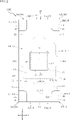
- FIG. 1 It is a top view of the semiconductor device which concerns on 1st Embodiment of this disclosure, and is transmitted through a sealing resin. It is a bottom view of the semiconductor device shown in FIG. 1. It is a right side view of the semiconductor device shown in FIG. 1. It is a front view of the semiconductor device shown in FIG. 1. It is sectional drawing which follows the VV line of FIG. It is sectional drawing which follows the VI-VI line of FIG. It is a partially enlarged view of FIG. It is a partially enlarged view of FIG. It is sectional drawing explaining the manufacturing process of the semiconductor device shown in FIG. It is sectional drawing explaining the manufacturing process of the semiconductor device shown in FIG. It is sectional drawing explaining the manufacturing process of the semiconductor device shown in FIG. It is sectional drawing explaining the manufacturing process of the semiconductor device shown in FIG. It is sectional drawing explaining the manufacturing process of the semiconductor device shown in FIG.
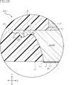
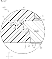
- FIG. 22 is a partially enlarged cross-sectional view of a modified example of the semiconductor device shown in FIG. 22. It is a partially enlarged sectional view of the semiconductor device which concerns on 4th Embodiment of this disclosure. It is a partially enlarged sectional view of the modification of the semiconductor device shown in FIG. It is a top view of the semiconductor device which concerns on 5th Embodiment of this disclosure, and is transmitted through a sealing resin. It is a bottom view of the semiconductor device shown in FIG. 26. It is a front view of the semiconductor device shown in FIG. 26.
- FIG. 22 is a partially enlarged cross-sectional view of a modified example of the semiconductor device shown in FIG. 22. It is a partially enlarged sectional view of the semiconductor device which concerns on 4th Embodiment of this disclosure. It is a partially enlarged sectional view of the modification of the semiconductor device shown in FIG. It is a top view of the semiconductor device which concerns on 5th Embodiment of this disclosure, and is transmitted through a sealing resin. It is
- FIG. 6 is a cross-sectional view taken along the line XXIX-XXIX of FIG. 26.
- FIG. 29 is a partially enlarged view.
- FIG. 26 is a partially enlarged cross-sectional view of a modified example of the semiconductor device shown in FIG. 26.
- the semiconductor device A10 includes a conductor 10, a semiconductor element 21, a plurality of wires 30, and a sealing resin 40.
- the semiconductor device A10 is, for example, a magnetic sensor (Hall IC) in which the semiconductor element 21 is a Hall element.
- the semiconductor device A10 is a resin package type that is surface-mounted on wiring boards of various electronic devices.
- the semiconductor element 21 is not limited to the Hall element, and may be another type of element supported by the conductor 10.
- FIG. 1 is transparent to the sealing resin 40 for convenience of understanding. In FIG. 1, the sealing resin 40 is shown by an imaginary line (dashed-dotted line).
- the semiconductor device A10 In the description of the semiconductor device A10 (and the semiconductor devices A20 to A50 described later), three directions orthogonal to each other (that is, the direction x, the direction y, and the direction z) are appropriately referred to.
- the direction z is a direction orthogonal to the main surface (or the back surface) of the conductor 10, and is also referred to as a “thickness direction (z)” of the conductor 10 (or a semiconductor element 21 or the like).
- the direction x and the direction y are referred to as “first direction (x)” and “second direction (y)”, respectively, but the present disclosure is not limited thereto.
- the semiconductor device A10 has a rectangular shape having a second direction y as a long side when viewed in the thickness direction z (in a plan view).
- the conductor 10 includes a die pad 101 and a plurality of terminals 102.
- the die pad 101 supports the semiconductor element 21.
- the plurality of terminals 102 are located apart from the die pad 101 and are arranged at the four corners of the semiconductor device A10 when viewed in the thickness direction z. The number and arrangement of the plurality of terminals 102 is not limited to this.
- the plurality of terminals 102 are conductive to the semiconductor element 21.
- the conductor 10 (die pad 101, a plurality of terminals 102) is made of a metal material.
- the composition of the metallic material comprises copper (Cu). In other words, the metallic material contains copper.
- the metal material is not limited to one containing copper as long as it is a non-magnetic material.
- the conductor 10 has a main surface 11 and a back surface 12.
- the main surface 11 is a combination of a plurality of regions (for example, a flat region) (the same applies to the back surface 12).
- the main surface 11 faces one side in the thickness direction z.
- the main surface 11 has a first edge 111.
- the first edge 111 refers to a plurality of sections (straight line portions) included in the peripheral edge of the main surface 11, and each section is in either the first direction x or the second direction y. It is extended.
- the back surface 12 faces the other side in the thickness direction z.
- the back surface 12 is exposed from the sealing resin 40.
- the back surface 12 is flush with the bottom surface of the sealing resin 40 (bottom surface 42 described later) and is not covered with the sealing resin 40.
- the back surface 12 has a second edge 121.
- the second edge 121 refers to a plurality of sections (straight line portions) included in the peripheral edge of the back surface 12, and each section extends in either the first direction x or the second direction y. ing.
- the first edge 111 is located outside the second edge 121 (in other words, the bottom surface 12 of the die pad 101) when viewed in the thickness direction z (see FIGS. 1 and 2). The first edge 111 is farther than the second edge 121 with respect to the center).
- the first edge 111 is located outside the second edge 121 (in other words, the first edge 111 is closer to the first edge 111 with reference to the center of the bottom surface 12 of each terminal 102. Is farther than the second edge 121).
- the entire back surface 12 overlaps the main surface 11, and the area of the back surface 12 is smaller than the area of the main surface 11.
- the distance D in the thickness direction z from the main surface 11 to the back surface 12 in the die pad 101 and each terminal 102 is equal to each other. In other words, the maximum thickness (distance D) of the die pad 101 and each terminal 102 is equal to each other.
- the main surface 11 of the conductor 10 may be configured with a metal plating layer.
- the composition of the metal plating layer contains, for example, silver (Ag).
- the composition of the metal plating layer may contain nickel (Ni) and palladium (Pd), or may contain nickel, palladium and gold (Au).
- the conductor 10 has at least one intermediate surface 13.
- the die pad 101 and the plurality of terminals 102 each have an intermediate surface 13.
- the intermediate surface 13 is connected to the first end edge 111 of the main surface 11 and the second end edge 121 of the back surface 12 (the same applies to each terminal 102).
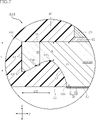
- the intermediate surface 13 in a cross section orthogonal to the direction in which the first edge 111 extends, is Includes first point 13A and second point 13B.
- the first point 13A is located between the first edge 111 and the second edge 121 in the cross section.
- the second point 13B is located between the first edge 111 and the first point 13A in the cross section. Further, the first distance d1 in the thickness direction z from the main surface 11 to the first point 13A is smaller than the second distance d2 in the thickness direction z from the main surface 11 to the second point 13B.
- the intermediate surface 13 includes an end portion (end surface portion) 131 and an overhanging portion (overhanging surface portion) 132.
- the end 131 extends from the first edge 111 of the main surface 11 to the other side in the thickness direction z. Further, the end portion 131 has a lower end edge (end edge 131A or "third end edge") and an upper end edge separated from each other in the thickness direction z.
- the overhanging portion 132 reaches the first point 13A of the intermediate surface 13 from the edge 131A.
- the second point 13B of the intermediate surface 13 is included in the overhanging portion 132.
- the second point 13B is a point located between the first edge 111 and the first point 13A of the intermediate surface 13, and the second distance d2 is larger than the first distance d1. It suffices if the conditions are met.
- the second point 13B may be a point that coincides with the edge 131A.
- the dimension t in the thickness direction z of the end portion 131 is smaller than the distance D in the thickness direction z from the main surface 11 to the back surface 12 of the conductor 10.
- the intermediate surface 13 is configured to be substantially entirely covered with the sealing resin 40 except for a part of the end portion 131 of the die pad 101 (see, for example, FIG. 6).
- the dimension t of the end portion 131 in the thickness direction z is a second distance d2 or more (t ⁇ d2) in the thickness direction z from the main surface 11 to the second point 13B of the intermediate surface 13.
- each of the plurality of terminals 102 has a side surface 14.
- the side surface 14 faces in a direction orthogonal to the thickness direction z and is connected to the main surface 11 and the back surface 12.
- the side surface 14 is exposed from the sealing resin 40.
- the side surface 14 includes a first surface 141 and a second surface 142.
- the first surface 141 faces the first direction x.
- the second surface 142 faces the second direction y and is connected to the first surface 141.
- the semiconductor element 21 is supported by the die pad 101 as shown in FIGS. 1, 5 and 6.
- the semiconductor element 21 has a rectangular shape when viewed in the thickness direction z.
- the semiconductor element 21 is a Hall element using, for example, gallium arsenide (GaAs) as a material.
- the Hall element has an advantage that the Hall voltage is excellent in linearity with respect to a change in magnetic flux density and is not easily affected by a temperature change.
- the semiconductor element 21 may be a Hall element using any one of silicon (Si), indium arsenide (InAs), and indium antimonide (InSb) as a material.
- the semiconductor device 21 has a plurality of electrodes 211.
- the plurality of electrodes 211 are located on one side of the thickness direction z in the semiconductor element 21.
- the plurality of electrodes 211 are conducting to a circuit configured inside the semiconductor element 21.
- the other side of the semiconductor element 21 in the thickness direction z is supported by the main surface 11 of the die pad 101 via the bonding layer 22.
- the bonding layer 22 is a die attach paste containing metal particles such as silver and a synthetic resin.
- the plurality of wires 30 are individually bonded to the plurality of electrodes 211 of the semiconductor element 21 and the main surface 11 of the plurality of terminals 102. As a result, the plurality of terminals 102 are electrically connected to the semiconductor element 21.
- the composition of the plurality of wires 30 includes, for example, gold.
- the sealing resin 40 covers the main surface 11 of the conductor 10, the semiconductor element 21, the plurality of wires 30, and at least a part of the intermediate surface 13 of the conductor 10. There is.
- the sealing resin 40 has electrical insulation.
- the sealing resin 40 is made of a material containing a thermosetting synthetic resin.
- the synthetic resin is, for example, a black epoxy resin.
- the sealing resin 40 has a top surface 41, a bottom surface 42, a pair of first side surfaces 43, and a pair of second side surfaces 44.
- the top surface 41 faces one side in the thickness direction z.
- the bottom surface 42 faces the other side in the thickness direction z.
- the back surface 12 of the conductor 10 is exposed from the bottom surface 42.
- the bottom surface 42 is flush with the back surface 12.
- the pair of first side surfaces 43 face each other in the first direction x and are connected to the top surface 41 and the bottom surface 42. From the pair of first side surfaces 43, the first surface 141 of the plurality of terminals 102 and a part of the end portion 131 of the die pad 101 are exposed. These portions exposed from the pair of first side surfaces 43 are flush with any of the pair of first side surfaces 43.
- the pair of second side surfaces 44 face each other in the second direction y and are connected to the top surface 41, the bottom surface 42, and the pair of first side surfaces 43.
- the second surface 142 of the plurality of terminals 102 is exposed from the pair of second side surfaces 44.
- the second surface 142 of each of the plurality of terminals 102 is flush with any of the pair of second side surfaces 44.
- the coating layer 50 covers the back surface 12 of the conductor 10.
- the coating layer 50 contains a metal element.
- the metal element covers at least one of nickel and palladium.
- the covering layer 50 has a first layer 51 and a second layer 52.
- the first layer 51 covers the back surface 12.
- the composition of the first layer 51 contains nickel.
- the second layer 52 is laminated on the first layer 51.
- the composition of the second layer 52 contains palladium.
- the semiconductor device A10 has a configuration in which the coating layer 50 includes a plurality of metal layers laminated in the thickness direction z.
- the coating layer 50 may be composed of a single metal layer.
- the composition of the metal layer comprises either nickel or palladium.
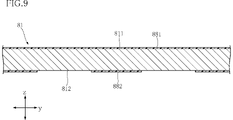
- each cross-sectional position of FIGS. 9 to 16 corresponds to the cross-sectional position of FIG. 5 of the semiconductor device A10.
- the first mask layer 881 covering the entire main surface 811 and one of the back surface 812.
- a second mask layer 882 that covers the portion is formed.
- the base material 81 is a thin metal plate containing, for example, copper in its composition.
- the thickness of the base material 81 is, for example, 100 ⁇ m.
- a part of the base material 81 corresponds to the conductor 10 of the semiconductor device A10.
- Each of the main surface 811 and the back surface 812 is a uniform flat surface.
- the first mask layer 881 is formed by applying a resist liquid used for photolithography to the main surface 811.
- the second mask layer 882 is formed by photolithography patterning.
- a part of the base material 81 is removed by the first wet etching.
- the etching solution is, for example, a mixed solution of H 2 SO 4 (sulfuric acid) and H 2 O 2 (hydrogen peroxide).
- H 2 SO 4 sulfuric acid
- H 2 O 2 hydrogen peroxide
- a part of the base material 81 is removed by the second wet etching.
- the base material 81 is formed with a second concave surface 814 that is recessed from the first concave surface 813 in the thickness direction z.
- a fourth mask layer 884 that covers the entire back surface 812 and the second concave surface 814 is formed.
- the fourth mask layer 884 is formed by photolithography patterning.
- the opening 881A in the first mask layer 881 by photolithography patterning the region of the main surface 811 overlapping the first concave surface 813 in the thickness direction z is exposed from the first mask layer 881.
- a part of the base material 81 is removed by the third wet etching. Partial removal of the base material 81 is performed from both sides of the base material 81 in the thickness direction z. By removing a part of the base material 81 in this step, the base material 81 is formed with an end surface 815 that faces in a direction orthogonal to the thickness direction z and is connected to the main surface 811 and the second concave surface 814. Orthogonal. After that, the first mask layer 881 and the fourth mask layer 884 are removed. By going through this step, the main surface 811 becomes the main surface 11 of the conductor 10, and the back surface 812 becomes the back surface 12 of the conductor 10. Further, the second concave surface 814 and the end surface 815 become the intermediate surface 13 of the conductor 10.
- the semiconductor element 21 is supported by the base material 81.
- the bonding material 82 is applied to the main surface 811 of the base material 81.
- the joining material 82 is, for example, a conductive paste containing silver.
- the semiconductor element 21 adsorbed by a collet or the like is transferred onto the base material 81, and then the semiconductor element 21 is adhered to the bonding material 82.
- the joining material 82 is thermoset in a curing furnace or the like.
- the thermosetting bonding material 82 corresponds to the bonding layer 22 of the semiconductor device A10.
- a plurality of wires 30 bonded to the semiconductor element 21 and the base material 81 are formed.
- the plurality of wires 30 are formed by wire bonding.
- a sealing resin 83 that covers a part of the base material 81, the semiconductor element 21, and the plurality of wires 30 is formed.
- the sealing resin 83 is formed by thermosetting a thermosetting synthetic resin having electrical insulation by transfer molding. By going through this step, the main surface 11 and the intermediate surface 13 of the base material 81 are covered with the sealing resin 83, and the back surface 12 of the base material 81 is exposed from the sealing resin 83.
- a covering layer 50 covering the back surface 812 of the base material 81 is formed.
- the coating layer 50 is formed by electrolytic plating using the base material 81 as a conductive path.
- each of the semiconductor elements 21 is one. Divide into pieces containing. In cutting, for example, a dicing saw is used to cut from the side facing the back surface 12 of the base material 81 in the thickness direction z. When cutting along the first direction x, cutting is performed along the cutting line CL shown in FIG. The individual pieces divided in this step become the semiconductor device A10. At this time, the base material 81 becomes the conductor 10 of the semiconductor device A10 including the die pad 101 and the plurality of terminals 102. The sealing resin 83 becomes the sealing resin 40 of the semiconductor device A10. Through the above steps, the semiconductor device A10 is manufactured.
- a semiconductor device A11 which is a first modification of the semiconductor device A10, will be described with reference to FIG.
- the cross-sectional position of FIG. 17 corresponds to the cross-sectional position of FIG. 7 of the semiconductor device A10.
- the configuration of the intermediate surface 13 of the conductor 10 is different from that of the semiconductor device A10.
- the semiconductor device A11 has a configuration in which a clear end portion 131 and an overhanging portion 132 do not appear on the intermediate surface 13.
- the conductor 10 sandwiched between the section of the intermediate surface 13 from the first edge 111 to the first point 13A and the main surface 11.
- the average thickness of the portion is relatively smaller than the average thickness of the portion of the semiconductor device A10.
- the first distance d1 in the thickness direction z from the main surface 11 to the first point 13A of the intermediate surface 13 is the thickness direction z from the main surface 11 to the second point 13B of the intermediate surface 13.
- a relationship smaller than the second distance d2 is established.
- a semiconductor device A12 which is a second modification of the semiconductor device A10, will be described with reference to FIG.
- the cross-sectional position of FIG. 18 corresponds to the cross-sectional position of FIG. 7 of the semiconductor device A10.
- the configuration of the intermediate surface 13 of the conductor 10 is different from that of the semiconductor device A10.
- the overhanging portion 132 of the intermediate surface 13 includes the first region 132A and the second region 132B. Both the first region 132A and the second region 132B are flat surfaces facing the other side in the thickness direction z. Seen in the thickness direction z, the first region 132A is located between the first edge 111 of the main surface 11 and the second region 132B. In the thickness direction z, the second region 132B is located between the main surface 11 and the first region 132A. The first point 13A of the intermediate surface 13 is included in the first region 132A.
- the first point 13A may take any position in the first region 132A.
- the second point 13B of the intermediate surface 13 is included in the second region 132B.
- the second point 13B may take any position in the second region 132B.
- FIG. 19 Based on FIG. 19, the semiconductor device A13, which is a third modification of the semiconductor device A10, will be described.
- the cross-sectional position of FIG. 19 corresponds to the cross-sectional position of FIG. 7 of the semiconductor device A10.
- the configuration of the intermediate surface 13 of the conductor 10 is different from that of the semiconductor device A10.
- the surface roughness of the end portion 131 of the intermediate surface 13 is larger than the surface roughness of the overhanging portion 132 of the intermediate surface 13.
- This configuration is obtained by applying a chemical solution to the end face 815 of the base material 81 in the manufacturing process of the semiconductor device A10 shown in FIG.
- a chemical solution either an acidic solution or an alkaline solution is selected.
- An example of an acidic solution is a mixed solution of sulfuric acid and hydrogen peroxide.
- An example of an alkaline solution is an aqueous solution of ammonium formate (NH 4 HCO 2 ).
- the semiconductor device A10 is connected to a main surface 11 including the first edge 111, a back surface 12 including the second edge 121 and exposed from the sealing resin 40, and the first edge 111 and the second edge 121.
- a conductor 10 having an intermediate surface 13 is provided.
- the first edge 111 is located outward of the second edge 121 when viewed in the thickness direction z.
- the intermediate surface 13 includes a first point 13A located between the first edge 111 and the second edge 121, and the first edge 111. It includes a second point 13B located between the first point 13A and the first point 13A.
- the first distance d1 in the thickness direction z from the main surface 11 to the first point 13A is smaller than the second distance d2 in the thickness direction z from the main surface 11 to the second point 13B.
- the intermediate surface 13 includes a section extending from the first point 13A to the first edge 111 on the other side in the thickness direction z. ..
- the semiconductor device A10 By providing the semiconductor device A10 with the above configuration, even when peeling occurs between the intermediate surface 13 and the sealing resin 40 starting from the second end edge 121, the first point 13A and the second point The region of the intermediate surface 13 (peeling restricted region) located between the 13B and 13B regulates the propagation of the peeling. Therefore, in the semiconductor device A10, it becomes difficult for the peeling to reach the edge 131A which is the boundary between the end 131 and the overhanging portion 132 shown in FIG. 7. Therefore, according to the semiconductor device A10, it is possible to more effectively suppress the peeling that occurs between the conductor 10 and the sealing resin 40.
- the intermediate surface 13 of the conductor 10 has an end portion 131 extending from the first end edge 111 of the main surface 11 to the other side in the thickness direction z, and an overhanging portion extending from the end edge 131A of the end portion 131 to the first point 13A. Includes 132 and.
- the dimension t of the end portion 131 in the thickness direction z is equal to or larger than the second distance d2 in the thickness direction z from the main surface 11 to the second point 13B.
- the section of the intermediate surface 13 extending from the first point 13A to the first edge 111 on the other side in the thickness direction z becomes longer. This contributes to the effective suppression of peeling that occurs between the conductor 10 and the sealing resin 40.
- the dimension t in the thickness direction z of the end 131 of the intermediate surface 13 is smaller than the distance D in the thickness direction z from the main surface 11 to the back surface 12 shown in FIG. As a result, the entire (or substantially the entire) intermediate surface 13 is covered with the sealing resin 40. This contributes to the improvement of the withstand voltage of the semiconductor device A10.
- the first distance d1 in the thickness direction z from the main surface 11 to the first point 13A of the intermediate surface 13 is from the main surface 11 to the intermediate surface 13.
- a relationship that is smaller than the second distance d2 in the thickness direction z reaching the second point 13B of the above is established. Therefore, even if there is a difference in the configuration of the intermediate surface 13 of the conductor 10, as long as the intermediate surface 13 satisfies this relationship, the peeling that occurs between the conductor 10 and the sealing resin 40 is more effectively suppressed. It plays an action effect.
- the surface roughness of the end portion 131 of the intermediate surface 13 is larger than the surface roughness of the overhanging portion 132 of the intermediate surface 13.
- the surface area of the end portion 131 is further expanded, so that the creepage distance of the end portion 131 from the end edge 131A of the end portion 131 to the first end edge 111 of the main surface 11 becomes longer. This contributes to the effective suppression of peeling that occurs between the conductor 10 and the sealing resin 40.
- the conductor 10 includes a die pad 101 that supports the semiconductor element 21 and a terminal 102 that conducts to the semiconductor element 21.
- the terminal 102 has a side surface 14 that faces a direction orthogonal to the thickness direction z and is connected to the main surface 11 and the back surface 12.
- the side surface 14 is exposed from the sealing resin 40.
- the semiconductor device A10 further includes a coating layer 50 that covers the back surface 12 of the conductor 10.
- the coating layer 50 contains a metal element.
- the metal element contained in the coating layer 50 contains at least one of nickel and palladium.
- the first layer 51 which covers the back surface 12 and contains nickel in the composition, and is laminated on the first layer 51, as in the semiconductor device A10.
- a coating layer 50 having a second layer 52 containing palladium in the composition.
- FIG. 20 is transparent to the sealing resin 40 for convenience of understanding.
- the permeated sealing resin 40 is shown by an imaginary line.
- the configuration of the coating layer 50 of the semiconductor device A20 is different from that of the semiconductor device A10 described above.
- the covering layer 50 includes a part of the end 131 of the die pad 101 and the side surfaces 14 (first surface 141 and first surface 141 and first surface 141) of the plurality of terminals 102. It covers the two sides 142).
- the coating layer 50 of the semiconductor device A20 is obtained by the following steps. After going through the steps shown in FIGS. 9 to 14 in the manufacture of the semiconductor device A10, the base material 81 and the sealing resin 83 are cut and divided into individual pieces as shown in FIG. Then, the coating layer 50 is obtained by forming a metal layer covering the exposed surface of the individual base material 81 by electroless plating.
- the semiconductor device A20 is connected to a main surface 11 including the first edge 111, a back surface 12 including the second edge 121 and exposed from the sealing resin 40, and the first edge 111 and the second edge 121.
- a conductor 10 having an intermediate surface 13 is provided.
- the first edge 111 is located outward of the second edge 121 when viewed in the thickness direction z.
- the intermediate surface 13 includes a first point 13A located between the first edge 111 and the second edge 121, and the first edge 111. It includes a second point 13B located between the first point 13A and the first point 13A.
- the first distance d1 in the thickness direction z from the main surface 11 to the first point 13A is smaller than the second distance d2 in the thickness direction z from the main surface 11 to the second point 13B. Therefore, the semiconductor device A20 can also more effectively suppress the peeling that occurs between the conductor 10 and the sealing resin 40.
- the coating layer 50 covers the side surface 14 of the terminal 102. This makes it possible to improve the wettability of the solder with respect to the side surface 14. Therefore, when the semiconductor device A10 is mounted on the wiring board, the growth of the solder fillet formed on the side surface 14 is promoted. This contributes to further improvement of the mounting strength of the semiconductor device A10 on the wiring board.
- the semiconductor device A30 according to the third embodiment of the present disclosure will be described with reference to FIG. 22.
- the same or similar elements of the above-mentioned semiconductor device A10 are designated by the same reference numerals, and duplicate description will be omitted.
- the cross-sectional position of FIG. 22 is the same as the cross-sectional position of FIG. 7 of the semiconductor device A10.
- the configuration of the intermediate surface 13 of the conductor 10 of the semiconductor device A30 is different from that of the semiconductor device A10 described above.
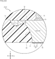
- the intermediate surface 13 includes the recess 133.
- the recess 133 is recessed on one side in the thickness direction z.
- the recess 133 is an element of the overhanging portion 132 of the intermediate surface 13.
- the recess 133 is located between the first edge 111 of the main surface 11 and the first point 13A of the intermediate surface 13 when viewed in the thickness direction z.
- the dimension t in the thickness direction z of the end 131 of the intermediate surface 13 is the thth dimension t in the thickness direction z from the main surface 11 to the second point 13B of the intermediate surface 13. It is smaller than 2 distance d2.
- the dimension t of the end portion 131 in the thickness direction z may be the second distance d2 or more.
- the semiconductor device A31 which is a modification of the semiconductor device A30, will be described with reference to FIG. 23.
- the cross-sectional position of FIG. 23 corresponds to the cross-sectional position of FIG. 22 of the semiconductor device A30.
- the configuration of the intermediate surface 13 of the conductor 10 is different from that of the semiconductor device A30.
- the intermediate surface 13 includes the concave portion 133, the intermediate surface 13 does not have a clear end portion 131 and an overhanging portion 132.
- the conductor 10 sandwiched between the section of the intermediate surface 13 from the first edge 111 to the first point 13A and the main surface 11. The average thickness of the portion is relatively smaller than the average thickness of the portion of the semiconductor device A30.
- the first distance d1 in the thickness direction z from the main surface 11 to the first point 13A of the intermediate surface 13 is the thickness direction z from the main surface 11 to the second point 13B of the intermediate surface 13.
- a relationship smaller than the second distance d2 is established.
- the semiconductor device A30 is connected to a main surface 11 including the first edge 111, a back surface 12 including the second edge 121 and exposed from the sealing resin 40, and the first edge 111 and the second edge 121.
- a conductor 10 having an intermediate surface 13 is provided.
- the first edge 111 is located outward of the second edge 121 when viewed in the thickness direction z.
- the intermediate surface 13 includes a first point 13A located between the first edge 111 and the second edge 121, and the first edge 111. It includes a second point 13B located between the first point 13A and the first point 13A.
- the first distance d1 in the thickness direction z from the main surface 11 to the first point 13A is smaller than the second distance d2 in the thickness direction z from the main surface 11 to the second point 13B. Therefore, the semiconductor device A30 can also more effectively suppress the peeling that occurs between the conductor 10 and the sealing resin 40.
- the intermediate surface 13 of the conductor 10 includes a recess 133 recessed on one side in the thickness direction z.
- the recess 133 is located between the first edge 111 of the main surface 11 and the first point 13A of the intermediate surface 13 when viewed in the thickness direction z.
- a plurality of sections extending from the first point 13A to the first edge 111 on the other side in the thickness direction z are formed on the intermediate surface 13. Orthogonal.
- the semiconductor device A40 according to the fourth embodiment of the present disclosure will be described with reference to FIG. 24.
- the same or similar elements of the above-mentioned semiconductor device A10 are designated by the same reference numerals, and duplicate description will be omitted.
- the cross-sectional position of FIG. 24 corresponds to the cross-sectional position of FIG. 7 of the semiconductor device A10.
- the configuration of the intermediate surface 13 of the conductor 10 of the semiconductor device A40 is different from that of the semiconductor device A10 described above.
- the intermediate surface 13 includes a concave portion 133 and a convex portion 134.
- the configuration of the recess 133 is the same as that of the semiconductor device A30 described above.
- the convex portion 134 projects to the other side in the thickness direction z.
- the convex portion 134 is located between the first point 13A of the intermediate surface 13 and the second end edge 121 of the back surface 12 when viewed in the thickness direction z.
- the intermediate surface 13 may be configured to include the convex portion 134 but not the concave portion 133.
- the dimension t in the thickness direction z of the end 131 of the intermediate surface 13 is the thth dimension t in the thickness direction z from the main surface 11 to the second point 13B of the intermediate surface 13. It is smaller than 2 distance d2.
- the dimension t of the end portion 131 in the thickness direction z may be the second distance d2 or more.
- the semiconductor device A41 which is a modification of the semiconductor device A40, will be described with reference to FIG. 25.
- the cross-sectional position of FIG. 25 corresponds to the cross-sectional position of FIG. 24 of the semiconductor device A40.
- the configuration of the intermediate surface 13 of the conductor 10 is different from that of the semiconductor device A40.
- the intermediate surface 13 includes the concave portion 133 and the convex portion 134, but the intermediate surface 13 does not have a clear end portion 131 and an overhanging portion 132.
- the conductor 10 sandwiched between the section of the intermediate surface 13 from the first edge 111 to the first point 13A and the main surface 11. The average thickness of the portion is relatively smaller than the average thickness of the portion of the semiconductor device A40.
- the first distance d1 in the thickness direction z from the main surface 11 to the first point 13A of the intermediate surface 13 is the thickness direction z from the main surface 11 to the second point 13B of the intermediate surface 13.
- a relationship smaller than the second distance d2 is established.
- the semiconductor device A40 is connected to a main surface 11 including a first edge 111, a back surface 12 including a second edge 121 and exposed from the sealing resin 40, and the first edge 111 and the second edge 121.
- a conductor 10 having an intermediate surface 13 is provided.
- the first edge 111 is located outward of the second edge 121 when viewed in the thickness direction z.
- the intermediate surface 13 includes a first point 13A located between the first edge 111 and the second edge 121, and the first edge 111. It includes a second point 13B located between the first point 13A and the first point 13A.
- the first distance d1 in the thickness direction z from the main surface 11 to the first point 13A is smaller than the second distance d2 in the thickness direction z from the main surface 11 to the second point 13B. Therefore, the semiconductor device A40 can also more effectively suppress the peeling that occurs between the conductor 10 and the sealing resin 40.
- the intermediate surface 13 of the conductor 10 includes a concave portion 133 similar to that of the semiconductor device A30 and a convex portion 134 protruding to the other side in the thickness direction z.
- the convex portion 134 is located between the first point 13A of the intermediate surface 13 and the second end edge 121 of the back surface 12 when viewed in the thickness direction z.
- a section extending from the second edge 121 to the first point 13A on the other side in the thickness direction z is formed on the intermediate surface 13. ..
- the peeling generated between the conductor 10 and the sealing resin 40 can be regulated in more multiple steps.
- the semiconductor device A50 according to the fifth embodiment of the present disclosure will be described with reference to FIGS. 26 to 30.
- the same or similar elements of the above-mentioned semiconductor device A10 are designated by the same reference numerals, and duplicate description will be omitted.
- the configuration of the intermediate surface 13 of the conductor 10 of the semiconductor device A50 is different from that of the semiconductor device A10 described above.
- the dimension t of the end portion 131 of the intermediate surface 13 in the thickness direction z is the second distance d2 or more from the main surface 11 of the conductor 10 to the second point 13B of the intermediate surface 13. Further, the dimension t in the thickness direction z of the end portion 131 is equal to the distance D in the thickness direction z from the main surface 11 to the back surface 12 of the conductor 10.
- the overhanging portion 132 of the intermediate surface 13 is exposed from the bottom surface 42 of the sealing resin 40.
- the region of the overhanging portion 132 exposed from the sealing resin 40 extends along the first direction x.
- the region of the overhanging portion 132 exposed from the sealing resin 40 is covered with the coating layer 50.
- the semiconductor device A51 which is a modification of the semiconductor device A50, will be described with reference to FIG. 31.
- the cross-sectional position of FIG. 31 is the same as the cross-sectional position of FIG. 30 of the semiconductor device A50.
- the configuration of the intermediate surface 13 of the conductor 10 is different from that of the semiconductor device A50.
- the overhanging portion 132 of the intermediate surface 13 does not include a portion exposed from the bottom surface 42 of the sealing resin 40. Therefore, the entire overhanging portion 132 is covered with the sealing resin 40.
- the semiconductor device A50 is connected to a main surface 11 including a first edge 111, a back surface 12 including a second edge 121 and exposed from the sealing resin 40, and the first edge 111 and the second edge 121.
- a conductor 10 having an intermediate surface 13 is provided.
- the first edge 111 is located outward of the second edge 121 when viewed in the thickness direction z.
- the intermediate surface 13 includes a first point 13A located between the first edge 111 and the second edge 121, and the first edge 111. It includes a second point 13B located between the first point 13A and the first point 13A.
- the first distance d1 in the thickness direction z from the main surface 11 to the first point 13A is smaller than the second distance d2 in the thickness direction z from the main surface 11 to the second point 13B. Therefore, the semiconductor device A50 can also more effectively suppress the peeling that occurs between the conductor 10 and the sealing resin 40.
- the dimension t in the thickness direction z of the end portion 131 is equal to the distance D in the thickness direction z from the main surface 11 of the conductor 10 to the back surface 12.
- the section of the intermediate surface 13 extending from the first point 13A to the first edge 111 on the other side in the thickness direction z is the section of the semiconductor device A10. It will be even longer than the section. This contributes to the effective suppression of peeling that occurs between the conductor 10 and the sealing resin 40.
- the average thickness of the portion of the conductor 10 sandwiched between the main surface 11 and the overhanging portion 132 of the intermediate surface 13 becomes larger.
- the bending rigidity of the conductor 10 is increased, so that the bending deformation of the conductor 10 can be suppressed.
- the present disclosure is not limited to the above-described embodiment.
- the specific configuration of each part of the present disclosure can be freely redesigned.
- Appendix 1 Conductivity including a main surface having a first edge, a back surface separated from the main surface in the thickness direction and having a second edge, and an intermediate surface connected to the first edge and the second edge.
- a semiconductor element supported by the main surface and conductive to the conductor, A sealing resin that covers at least a part of the intermediate surface, the main surface, the semiconductor element, and the like.
- the back surface of the conductor is exposed from the sealing resin and Seen in the thickness direction, the first edge is located outward of the second edge.
- the intermediate surface is a first point located between the first edge and the second edge, and the first edge and the first point.
- the intermediate surface includes a recess recessed in the thickness direction.
- the semiconductor device according to Appendix 1 wherein the recess is located between the first edge and the first point when viewed in the thickness direction.
- the intermediate surface includes a convex portion protruding in the thickness direction.
- the semiconductor device according to Appendix 1 or 2 wherein the convex portion is located between the first point and the second edge when viewed in the thickness direction.
- the intermediate surface includes an end portion extending from the first end edge in the thickness direction and an overhanging portion, and the end portion is a third portion opposite to the first end edge in the thickness direction.
- Appendix 5. The semiconductor device according to Appendix 4, wherein the dimension of the end portion in the thickness direction is equal to or larger than the second distance.
- Appendix 6. The semiconductor device according to Appendix 4 or 5, wherein the dimension of the end portion in the thickness direction is smaller than the distance in the thickness direction from the main surface to the back surface.
- the semiconductor device according to Appendix 5, wherein the dimension of the end portion in the thickness direction is equal to the distance in the thickness direction from the main surface to the back surface.
- Appendix 8 The semiconductor device according to Appendix 7, wherein a part of the overhanging portion is exposed from the sealing resin.
- Appendix 9. The semiconductor device according to any one of Supplementary note 4 to 8, wherein the surface roughness of the end portion is larger than the surface roughness of the overhanging portion.
- the conductor includes a die pad and terminals spaced apart from the die pad.
- the die pad has a first main surface that forms part of the main surface of the conductor, and the terminal has a second main surface that forms another part of the main surface of the conductor.
- the semiconductor element is supported by the first main surface of the die pad, and is supported by the first main surface.
- Appendix 11. Further comprising a wire bonded to the second main surface of the semiconductor element and the terminal.
- the semiconductor device according to Appendix 10, wherein the wire is covered with the sealing resin.
- Appendix 12. The terminal has a first back surface forming a part of the back surface of the conductor, and has a side surface orthogonal to the thickness direction and connected to the second main surface and the first back surface.
- the terminal has an intermediate surface connected to the second main surface and the first back surface and at least partially covered with the sealing resin, and the intermediate surface is connected to the side surface.
- the semiconductor device according to 12. Appendix 14.
- a coating layer covering the back surface of the conductor is further provided.
- Appendix 15. The semiconductor device according to Appendix 14, wherein the conductor has a side surface connected to the main surface and the back surface and exposed from the sealing resin, and the side surface is covered with the coating layer.
- Appendix 16 The semiconductor device according to Appendix 14 or 15, wherein the metal element contains at least one of nickel and palladium.
- A10, A20, A30, A40, A50 Semiconductor device 10: Conductor 101: Die pad 102: Terminal 11: Main surface 111: First end edge 12: Back surface 121: Second end edge 13: Intermediate surface 13A: First point 13B: 2nd point 131: End 131A: Edge edge (3rd end edge) 132: Overhanging portion 132A: First region 132B: Second region 133: Recessed portion 134: Convex portion 14: Side surface 141: First surface 142: Second surface 21: Semiconductor element 211: Electrode 22: Bonding layer 30: Wire 40 : Sealing resin 41: Top surface 42: Bottom surface 43: First side surface 44: Second side surface 50: Coating layer 51: First layer 52: Second layer 81: Base material 811: Main surface 812: Back surface 813: First Concave surface 814: Second concave surface 815: End surface 82: Bonding material 83: Sealing resin 881: First mask layer 881A: Opening 882: Second mask layer 883
Landscapes
- Structures Or Materials For Encapsulating Or Coating Semiconductor Devices Or Solid State Devices (AREA)
- Physics & Mathematics (AREA)
- Geometry (AREA)
Priority Applications (4)
| Application Number | Priority Date | Filing Date | Title |
|---|---|---|---|
| JP2022565164A JPWO2022113661A1 (https=) | 2020-11-30 | 2021-11-01 | |
| DE112021005724.3T DE112021005724T5 (de) | 2020-11-30 | 2021-11-01 | Halbleiterbauteil |
| US18/254,310 US20230411232A1 (en) | 2020-11-30 | 2021-11-01 | Semiconductor device |
| CN202180080040.XA CN116670820A (zh) | 2020-11-30 | 2021-11-01 | 半导体器件 |
Applications Claiming Priority (2)
| Application Number | Priority Date | Filing Date | Title |
|---|---|---|---|
| JP2020198250 | 2020-11-30 | ||
| JP2020-198250 | 2020-11-30 |
Publications (1)
| Publication Number | Publication Date |
|---|---|
| WO2022113661A1 true WO2022113661A1 (ja) | 2022-06-02 |
Family
ID=81754394
Family Applications (1)
| Application Number | Title | Priority Date | Filing Date |
|---|---|---|---|
| PCT/JP2021/040269 Ceased WO2022113661A1 (ja) | 2020-11-30 | 2021-11-01 | 半導体装置 |
Country Status (5)
| Country | Link |
|---|---|
| US (1) | US20230411232A1 (https=) |
| JP (1) | JPWO2022113661A1 (https=) |
| CN (1) | CN116670820A (https=) |
| DE (1) | DE112021005724T5 (https=) |
| WO (1) | WO2022113661A1 (https=) |
Citations (9)
| Publication number | Priority date | Publication date | Assignee | Title |
|---|---|---|---|---|
| JP2004022725A (ja) * | 2002-06-14 | 2004-01-22 | Renesas Technology Corp | 半導体装置 |
| JP2005311099A (ja) * | 2004-04-22 | 2005-11-04 | Toshiba Corp | 半導体装置及びその製造方法 |
| JP2008258411A (ja) * | 2007-04-05 | 2008-10-23 | Rohm Co Ltd | 半導体装置および半導体装置の製造方法 |
| JP3161823U (ja) * | 2010-04-29 | 2010-08-12 | 坤遠科技股▲ふん▼有限公司 | 封止樹脂接合度を強化できるリードフレーム及びそのパッケージ構造 |
| JP2015038917A (ja) * | 2013-03-28 | 2015-02-26 | 大日本印刷株式会社 | リードフレーム、樹脂付きリードフレーム、リードフレームの多面付け体、樹脂付きリードフレームの多面付け体、光半導体装置、光半導体装置の多面付け体 |
| JP2016105432A (ja) * | 2014-12-01 | 2016-06-09 | Shマテリアル株式会社 | リードフレームの製造方法 |
| JP2017163086A (ja) * | 2016-03-11 | 2017-09-14 | Shマテリアル株式会社 | 光半導体素子搭載用のリードフレーム及びその製造方法 |
| JP2018190882A (ja) * | 2017-05-10 | 2018-11-29 | ローム株式会社 | 半導体装置 |
| JP2019047112A (ja) * | 2017-09-04 | 2019-03-22 | ローム株式会社 | 半導体装置 |
Family Cites Families (10)
| Publication number | Priority date | Publication date | Assignee | Title |
|---|---|---|---|---|
| EP0895287A3 (en) * | 1997-07-31 | 2006-04-05 | Matsushita Electric Industrial Co., Ltd. | Semiconductor device and lead frame for the same |
| US6927483B1 (en) * | 2003-03-07 | 2005-08-09 | Amkor Technology, Inc. | Semiconductor package exhibiting efficient lead placement |
| US20050146057A1 (en) * | 2003-12-31 | 2005-07-07 | Khor Ah L. | Micro lead frame package having transparent encapsulant |
| US20060071351A1 (en) * | 2004-09-28 | 2006-04-06 | Texas Instruments Incorporated | Mold compound interlocking feature to improve semiconductor package strength |
| US8492883B2 (en) * | 2008-03-14 | 2013-07-23 | Advanced Semiconductor Engineering, Inc. | Semiconductor package having a cavity structure |
| US8124447B2 (en) * | 2009-04-10 | 2012-02-28 | Advanced Semiconductor Engineering, Inc. | Manufacturing method of advanced quad flat non-leaded package |
| US8203201B2 (en) * | 2010-03-26 | 2012-06-19 | Stats Chippac Ltd. | Integrated circuit packaging system with leads and method of manufacture thereof |
| US9570381B2 (en) * | 2015-04-02 | 2017-02-14 | Advanced Semiconductor Engineering, Inc. | Semiconductor packages and related manufacturing methods |
| US10529672B2 (en) * | 2017-08-31 | 2020-01-07 | Stmicroelectronics, Inc. | Package with interlocking leads and manufacturing the same |
| US11569179B2 (en) * | 2020-11-19 | 2023-01-31 | Advanced Semiconductor Engineering, Inc. | Package structure including an outer lead portion and an inner lead portion and method for manufacturing package structure |
-
2021
- 2021-11-01 DE DE112021005724.3T patent/DE112021005724T5/de active Pending
- 2021-11-01 JP JP2022565164A patent/JPWO2022113661A1/ja active Pending
- 2021-11-01 WO PCT/JP2021/040269 patent/WO2022113661A1/ja not_active Ceased
- 2021-11-01 CN CN202180080040.XA patent/CN116670820A/zh active Pending
- 2021-11-01 US US18/254,310 patent/US20230411232A1/en active Pending
Patent Citations (9)
| Publication number | Priority date | Publication date | Assignee | Title |
|---|---|---|---|---|
| JP2004022725A (ja) * | 2002-06-14 | 2004-01-22 | Renesas Technology Corp | 半導体装置 |
| JP2005311099A (ja) * | 2004-04-22 | 2005-11-04 | Toshiba Corp | 半導体装置及びその製造方法 |
| JP2008258411A (ja) * | 2007-04-05 | 2008-10-23 | Rohm Co Ltd | 半導体装置および半導体装置の製造方法 |
| JP3161823U (ja) * | 2010-04-29 | 2010-08-12 | 坤遠科技股▲ふん▼有限公司 | 封止樹脂接合度を強化できるリードフレーム及びそのパッケージ構造 |
| JP2015038917A (ja) * | 2013-03-28 | 2015-02-26 | 大日本印刷株式会社 | リードフレーム、樹脂付きリードフレーム、リードフレームの多面付け体、樹脂付きリードフレームの多面付け体、光半導体装置、光半導体装置の多面付け体 |
| JP2016105432A (ja) * | 2014-12-01 | 2016-06-09 | Shマテリアル株式会社 | リードフレームの製造方法 |
| JP2017163086A (ja) * | 2016-03-11 | 2017-09-14 | Shマテリアル株式会社 | 光半導体素子搭載用のリードフレーム及びその製造方法 |
| JP2018190882A (ja) * | 2017-05-10 | 2018-11-29 | ローム株式会社 | 半導体装置 |
| JP2019047112A (ja) * | 2017-09-04 | 2019-03-22 | ローム株式会社 | 半導体装置 |
Also Published As
| Publication number | Publication date |
|---|---|
| JPWO2022113661A1 (https=) | 2022-06-02 |
| CN116670820A (zh) | 2023-08-29 |
| DE112021005724T5 (de) | 2023-08-10 |
| US20230411232A1 (en) | 2023-12-21 |
Similar Documents
| Publication | Publication Date | Title |
|---|---|---|
| TW398063B (en) | Lead frame and its manufacturing method thereof | |
| JP7520177B2 (ja) | 半導体装置 | |
| JP5141076B2 (ja) | 半導体装置 | |
| JP7089388B2 (ja) | 半導体装置および半導体装置の製造方法 | |
| JP7173487B2 (ja) | 半導体装置 | |
| JP7569912B2 (ja) | 半導体装置 | |
| CN113424311B (zh) | 半导体器件和半导体器件的制造方法 | |
| JP2022143166A (ja) | 半導体装置 | |
| JP7147501B2 (ja) | 半導体装置の製造方法 | |
| JP7193284B2 (ja) | リードフレーム及びリードフレームの製造方法 | |
| JP7594950B2 (ja) | 半導体装置 | |
| JP2019121698A (ja) | 半導体装置および半導体装置の製造方法 | |
| JP6718754B2 (ja) | 半導体装置 | |
| US20220173017A1 (en) | Semiconductor device | |
| JP2022143167A (ja) | 半導体装置 | |
| WO2022113661A1 (ja) | 半導体装置 | |
| JP7022541B2 (ja) | 半導体装置 | |
| JP2006147918A (ja) | 半導体装置 | |
| JP2023060343A (ja) | 半導体モジュール | |
| JP7154818B2 (ja) | 半導体装置および半導体装置の製造方法 | |
| US20250372485A1 (en) | Semiconductor device | |
| US20250379126A1 (en) | Semiconductor device and method of manufacturing semiconductor device | |
| JP7430988B2 (ja) | 電子装置 | |
| WO2024101174A1 (ja) | 半導体装置 | |
| JP2023179984A (ja) | リードフレームおよび電子部品 |
Legal Events
| Date | Code | Title | Description |
|---|---|---|---|
| 121 | Ep: the epo has been informed by wipo that ep was designated in this application |
Ref document number: 21897637 Country of ref document: EP Kind code of ref document: A1 |
|
| ENP | Entry into the national phase |
Ref document number: 2022565164 Country of ref document: JP Kind code of ref document: A |
|
| WWE | Wipo information: entry into national phase |
Ref document number: 202180080040.X Country of ref document: CN |
|
| 122 | Ep: pct application non-entry in european phase |
Ref document number: 21897637 Country of ref document: EP Kind code of ref document: A1 |