WO2022085566A1 - 実装基板、及び回路基板 - Google Patents
実装基板、及び回路基板 Download PDFInfo
- Publication number
- WO2022085566A1 WO2022085566A1 PCT/JP2021/038082 JP2021038082W WO2022085566A1 WO 2022085566 A1 WO2022085566 A1 WO 2022085566A1 JP 2021038082 W JP2021038082 W JP 2021038082W WO 2022085566 A1 WO2022085566 A1 WO 2022085566A1
- Authority
- WO
- WIPO (PCT)
- Prior art keywords
- dimension
- resin layer
- terminal
- terminals
- electronic component
- Prior art date
- Legal status (The legal status is an assumption and is not a legal conclusion. Google has not performed a legal analysis and makes no representation as to the accuracy of the status listed.)
- Ceased
Links
Images



Classifications
-
- H—ELECTRICITY
- H05—ELECTRIC TECHNIQUES NOT OTHERWISE PROVIDED FOR
- H05K—PRINTED CIRCUITS; CASINGS OR CONSTRUCTIONAL DETAILS OF ELECTRIC APPARATUS; MANUFACTURE OF ASSEMBLAGES OF ELECTRICAL COMPONENTS
- H05K3/00—Apparatus or processes for manufacturing printed circuits
- H05K3/22—Secondary treatment of printed circuits
- H05K3/28—Applying non-metallic protective coatings
-
- H—ELECTRICITY
- H10—SEMICONDUCTOR DEVICES; ELECTRIC SOLID-STATE DEVICES NOT OTHERWISE PROVIDED FOR
- H10H—INORGANIC LIGHT-EMITTING SEMICONDUCTOR DEVICES HAVING POTENTIAL BARRIERS
- H10H20/00—Individual inorganic light-emitting semiconductor devices having potential barriers, e.g. light-emitting diodes [LED]
- H10H20/80—Constructional details
- H10H20/85—Packages
- H10H20/857—Interconnections, e.g. lead-frames, bond wires or solder balls
-
- H—ELECTRICITY
- H05—ELECTRIC TECHNIQUES NOT OTHERWISE PROVIDED FOR
- H05K—PRINTED CIRCUITS; CASINGS OR CONSTRUCTIONAL DETAILS OF ELECTRIC APPARATUS; MANUFACTURE OF ASSEMBLAGES OF ELECTRICAL COMPONENTS
- H05K1/00—Printed circuits
- H05K1/18—Printed circuits structurally associated with non-printed electric components
- H05K1/181—Printed circuits structurally associated with non-printed electric components associated with surface mounted components
-
- H—ELECTRICITY
- H05—ELECTRIC TECHNIQUES NOT OTHERWISE PROVIDED FOR
- H05K—PRINTED CIRCUITS; CASINGS OR CONSTRUCTIONAL DETAILS OF ELECTRIC APPARATUS; MANUFACTURE OF ASSEMBLAGES OF ELECTRICAL COMPONENTS
- H05K1/00—Printed circuits
- H05K1/18—Printed circuits structurally associated with non-printed electric components
- H05K1/182—Printed circuits structurally associated with non-printed electric components associated with components mounted in printed circuit boards [PCB], e.g. insert-mounted components [IMC]
-
- H—ELECTRICITY
- H05—ELECTRIC TECHNIQUES NOT OTHERWISE PROVIDED FOR
- H05K—PRINTED CIRCUITS; CASINGS OR CONSTRUCTIONAL DETAILS OF ELECTRIC APPARATUS; MANUFACTURE OF ASSEMBLAGES OF ELECTRICAL COMPONENTS
- H05K3/00—Apparatus or processes for manufacturing printed circuits
- H05K3/30—Assembling printed circuits with electric components, e.g. with resistors
- H05K3/32—Assembling printed circuits with electric components, e.g. with resistors electrically connecting electric components or wires to printed circuits
- H05K3/34—Assembling printed circuits with electric components, e.g. with resistors electrically connecting electric components or wires to printed circuits by soldering
-
- H—ELECTRICITY
- H05—ELECTRIC TECHNIQUES NOT OTHERWISE PROVIDED FOR
- H05K—PRINTED CIRCUITS; CASINGS OR CONSTRUCTIONAL DETAILS OF ELECTRIC APPARATUS; MANUFACTURE OF ASSEMBLAGES OF ELECTRICAL COMPONENTS
- H05K3/00—Apparatus or processes for manufacturing printed circuits
- H05K3/30—Assembling printed circuits with electric components, e.g. with resistors
- H05K3/32—Assembling printed circuits with electric components, e.g. with resistors electrically connecting electric components or wires to printed circuits
- H05K3/34—Assembling printed circuits with electric components, e.g. with resistors electrically connecting electric components or wires to printed circuits by soldering
- H05K3/3452—Solder masks
-
- H—ELECTRICITY
- H10—SEMICONDUCTOR DEVICES; ELECTRIC SOLID-STATE DEVICES NOT OTHERWISE PROVIDED FOR
- H10H—INORGANIC LIGHT-EMITTING SEMICONDUCTOR DEVICES HAVING POTENTIAL BARRIERS
- H10H20/00—Individual inorganic light-emitting semiconductor devices having potential barriers, e.g. light-emitting diodes [LED]
- H10H20/80—Constructional details
- H10H20/85—Packages
- H10H20/852—Encapsulations
- H10H20/853—Encapsulations characterised by their shape
-
- H—ELECTRICITY
- H10—SEMICONDUCTOR DEVICES; ELECTRIC SOLID-STATE DEVICES NOT OTHERWISE PROVIDED FOR
- H10W—GENERIC PACKAGES, INTERCONNECTIONS, CONNECTORS OR OTHER CONSTRUCTIONAL DETAILS OF DEVICES COVERED BY CLASS H10
- H10W70/00—Package substrates; Interposers; Redistribution layers [RDL]
- H10W70/60—Insulating or insulated package substrates; Interposers; Redistribution layers
-
- H—ELECTRICITY
- H05—ELECTRIC TECHNIQUES NOT OTHERWISE PROVIDED FOR
- H05K—PRINTED CIRCUITS; CASINGS OR CONSTRUCTIONAL DETAILS OF ELECTRIC APPARATUS; MANUFACTURE OF ASSEMBLAGES OF ELECTRICAL COMPONENTS
- H05K2201/00—Indexing scheme relating to printed circuits covered by H05K1/00
- H05K2201/09—Shape and layout
- H05K2201/09209—Shape and layout details of conductors
- H05K2201/09372—Pads and lands
- H05K2201/09472—Recessed pad for surface mounting; Recessed electrode of component
-
- H—ELECTRICITY
- H05—ELECTRIC TECHNIQUES NOT OTHERWISE PROVIDED FOR
- H05K—PRINTED CIRCUITS; CASINGS OR CONSTRUCTIONAL DETAILS OF ELECTRIC APPARATUS; MANUFACTURE OF ASSEMBLAGES OF ELECTRICAL COMPONENTS
- H05K2201/00—Indexing scheme relating to printed circuits covered by H05K1/00
- H05K2201/09—Shape and layout
- H05K2201/09818—Shape or layout details not covered by a single group of H05K2201/09009 - H05K2201/09809
- H05K2201/09827—Tapered, e.g. tapered hole, via or groove
-
- H—ELECTRICITY
- H05—ELECTRIC TECHNIQUES NOT OTHERWISE PROVIDED FOR
- H05K—PRINTED CIRCUITS; CASINGS OR CONSTRUCTIONAL DETAILS OF ELECTRIC APPARATUS; MANUFACTURE OF ASSEMBLAGES OF ELECTRICAL COMPONENTS
- H05K2201/00—Indexing scheme relating to printed circuits covered by H05K1/00
- H05K2201/10—Details of components or other objects attached to or integrated in a printed circuit board
- H05K2201/10007—Types of components
- H05K2201/10106—Light emitting diode [LED]
-
- H—ELECTRICITY
- H10—SEMICONDUCTOR DEVICES; ELECTRIC SOLID-STATE DEVICES NOT OTHERWISE PROVIDED FOR
- H10H—INORGANIC LIGHT-EMITTING SEMICONDUCTOR DEVICES HAVING POTENTIAL BARRIERS
- H10H20/00—Individual inorganic light-emitting semiconductor devices having potential barriers, e.g. light-emitting diodes [LED]
- H10H20/01—Manufacture or treatment
- H10H20/036—Manufacture or treatment of packages
- H10H20/0364—Manufacture or treatment of packages of interconnections
-
- H—ELECTRICITY
- H10—SEMICONDUCTOR DEVICES; ELECTRIC SOLID-STATE DEVICES NOT OTHERWISE PROVIDED FOR
- H10W—GENERIC PACKAGES, INTERCONNECTIONS, CONNECTORS OR OTHER CONSTRUCTIONAL DETAILS OF DEVICES COVERED BY CLASS H10
- H10W72/00—Interconnections or connectors in packages
- H10W72/071—Connecting or disconnecting
- H10W72/072—Connecting or disconnecting of bump connectors
-
- H—ELECTRICITY
- H10—SEMICONDUCTOR DEVICES; ELECTRIC SOLID-STATE DEVICES NOT OTHERWISE PROVIDED FOR
- H10W—GENERIC PACKAGES, INTERCONNECTIONS, CONNECTORS OR OTHER CONSTRUCTIONAL DETAILS OF DEVICES COVERED BY CLASS H10
- H10W72/00—Interconnections or connectors in packages
- H10W72/071—Connecting or disconnecting
- H10W72/072—Connecting or disconnecting of bump connectors
- H10W72/07231—Techniques
- H10W72/07236—Soldering or alloying
-
- H—ELECTRICITY
- H10—SEMICONDUCTOR DEVICES; ELECTRIC SOLID-STATE DEVICES NOT OTHERWISE PROVIDED FOR
- H10W—GENERIC PACKAGES, INTERCONNECTIONS, CONNECTORS OR OTHER CONSTRUCTIONAL DETAILS OF DEVICES COVERED BY CLASS H10
- H10W72/00—Interconnections or connectors in packages
- H10W72/20—Bump connectors, e.g. solder bumps or copper pillars; Dummy bumps; Thermal bumps
-
- H—ELECTRICITY
- H10—SEMICONDUCTOR DEVICES; ELECTRIC SOLID-STATE DEVICES NOT OTHERWISE PROVIDED FOR
- H10W—GENERIC PACKAGES, INTERCONNECTIONS, CONNECTORS OR OTHER CONSTRUCTIONAL DETAILS OF DEVICES COVERED BY CLASS H10
- H10W72/00—Interconnections or connectors in packages
- H10W72/20—Bump connectors, e.g. solder bumps or copper pillars; Dummy bumps; Thermal bumps
- H10W72/241—Dispositions, e.g. layouts
-
- H—ELECTRICITY
- H10—SEMICONDUCTOR DEVICES; ELECTRIC SOLID-STATE DEVICES NOT OTHERWISE PROVIDED FOR
- H10W—GENERIC PACKAGES, INTERCONNECTIONS, CONNECTORS OR OTHER CONSTRUCTIONAL DETAILS OF DEVICES COVERED BY CLASS H10
- H10W72/00—Interconnections or connectors in packages
- H10W72/20—Bump connectors, e.g. solder bumps or copper pillars; Dummy bumps; Thermal bumps
- H10W72/251—Materials
- H10W72/252—Materials comprising solid metals or solid metalloids, e.g. PbSn, Ag or Cu
-
- H—ELECTRICITY
- H10—SEMICONDUCTOR DEVICES; ELECTRIC SOLID-STATE DEVICES NOT OTHERWISE PROVIDED FOR
- H10W—GENERIC PACKAGES, INTERCONNECTIONS, CONNECTORS OR OTHER CONSTRUCTIONAL DETAILS OF DEVICES COVERED BY CLASS H10
- H10W74/00—Encapsulations, e.g. protective coatings
- H10W74/10—Encapsulations, e.g. protective coatings characterised by their shape or disposition
- H10W74/15—Encapsulations, e.g. protective coatings characterised by their shape or disposition on active surfaces of flip-chip devices, e.g. underfills
-
- H—ELECTRICITY
- H10—SEMICONDUCTOR DEVICES; ELECTRIC SOLID-STATE DEVICES NOT OTHERWISE PROVIDED FOR
- H10W—GENERIC PACKAGES, INTERCONNECTIONS, CONNECTORS OR OTHER CONSTRUCTIONAL DETAILS OF DEVICES COVERED BY CLASS H10
- H10W90/00—Package configurations
- H10W90/701—Package configurations characterised by the relative positions of pads or connectors relative to package parts
- H10W90/721—Package configurations characterised by the relative positions of pads or connectors relative to package parts of bump connectors
- H10W90/724—Package configurations characterised by the relative positions of pads or connectors relative to package parts of bump connectors between a chip and a stacked insulating package substrate, interposer or RDL
-
- H—ELECTRICITY
- H10—SEMICONDUCTOR DEVICES; ELECTRIC SOLID-STATE DEVICES NOT OTHERWISE PROVIDED FOR
- H10W—GENERIC PACKAGES, INTERCONNECTIONS, CONNECTORS OR OTHER CONSTRUCTIONAL DETAILS OF DEVICES COVERED BY CLASS H10
- H10W90/00—Package configurations
- H10W90/701—Package configurations characterised by the relative positions of pads or connectors relative to package parts
- H10W90/731—Package configurations characterised by the relative positions of pads or connectors relative to package parts of die-attach connectors
- H10W90/734—Package configurations characterised by the relative positions of pads or connectors relative to package parts of die-attach connectors between a chip and a stacked insulating package substrate, interposer or RDL
Definitions
- This disclosure relates to a mounting board and a circuit board.
- Patent Document 1 a technique for forming a protrusion between a pair of terminals is disclosed.
- the mounting board according to the present disclosure is a mounting board including an electronic component having at least a pair of first terminals and a circuit board having at least a pair of second terminals, the first terminal and the second.
- the terminals of the above are joined by a joining material, and the first terminal, the second terminal, and the joining material are arranged in a recess formed in the resin layer, so that the periphery is surrounded by the resin layer, and the first terminal is formed.
- the total thickness of the terminal, the second terminal, and the bonding material is the dimension h1
- the dimension h1 is 1 ⁇ m or more and 20 ⁇ m or less
- the width of the first terminal is the dimension d1 of the resin layer.
- the width of the recess is dimension d2
- the value of (dimension d2-dimension d1) is 10 ⁇ m or less.
- the first terminal, the second terminal, and the joining material are arranged in the recess formed in the resin layer, so that the periphery is surrounded by the resin layer.
- the dimension h1 which is the total thickness of the first terminal, the second terminal, and the joint material to be 1 ⁇ m or more and 20 ⁇ m or less, the joint portion can be made difficult to break.
- the value of (dimension d2-dimension d1) to 10 ⁇ m or less, it is possible to prevent the electronic components from peeling off from the circuit board when the mounting substrate receives a physical impact.
- a constituent material may be arranged between the joining material and the resin layer. As a result, by supporting the electronic components with the constituent materials, it is possible to further prevent the electronic components from peeling off from the circuit board.
- a component may be arranged between the resin layer existing between the pair of first terminals and the main body of the electronic component. As a result, the main body of the electronic component can be held by the constituent material, and the strength can be improved.
- the constituent material may come into contact with the main body.
- the lower surface of the main body of the electronic component can be fixed with the constituent material. Therefore, even if the mounting board receives a physical impact, it becomes difficult for a force to be applied to the joining material and the electronic components are hard to be peeled off from the circuit board.
- the resin layer existing between the pair of first terminals may come into contact with the main body of the electronic component.
- the lower surface of the main body of the electronic component is in contact with and supported by the resin layer, even if the mounting board receives a physical impact, it is difficult for a force to be applied to the bonding material and the electronic component is not easily peeled off from the circuit board. Become.
- the dimension R1 may be smaller than the dimension R2.
- the main body of the electronic component is surrounded and supported by the surrounding resin layer, even if the mounting board receives a physical impact, it becomes difficult to apply force to the bonding material, and the electronic component becomes It is difficult to peel off from the circuit board.
- the inner surface of the recess may have a tapered shape. Force is applied to the bonding material from the resin layer when a thermal shock is applied due to the difference in the coefficient of thermal expansion between the resin layer and the substrate. It becomes difficult for the electronic components to come off from the circuit board in the thermal shock test.
- the circuit board according to the present disclosure is a circuit board having at least a pair of second terminals, in which a bonding material is arranged on the second terminal, and the second terminal and the bonding material are formed in a resin layer.
- a bonding material is arranged on the second terminal, and the second terminal and the bonding material are formed in a resin layer.
- circuit board according to the present disclosure it is possible to obtain a mounting board having the same operation and effect as described above when electronic components are mounted.
- the dimension h2 may be larger than the thickness of the resin layer.
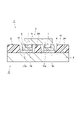
- FIG. 1 is a schematic cross-sectional view showing a mounting board 1 according to an embodiment of the present disclosure.
- the mounting board 1 includes an electronic component 2 and a circuit board 3.
- the mounting board 1 is configured by mounting the electronic component 2 on the circuit board 3 via the joining material 4.
- the electronic component 2 includes a main body 6 and a pair of terminals 7 (first terminal).
- the main body 6 is a member for exerting a function as an electronic component 2.
- the terminal 7 is a metal portion formed on the main surface of the main body 6.
- the electronic component 2 is composed of, for example, a micro LED or the like.
- the micro LED is a component that emits light in response to an input from the circuit board 3.
- the circuit board 3 includes a base material 8, a resin layer 9, and a pair of terminals 10 (second terminals).
- the base material 8 is a flat plate-shaped main body of the circuit board 3.
- the resin layer 9 is a resin layer formed on the upper surface of the base material 8.
- the terminal 10 is a metal portion formed on the main surface of the base material 8.
- Ni, Cu, Ti, Cr, Al, Mo, Pt, Au, an alloy selected from at least two of these, and the like are adopted.
- the joining material 4 is a member that joins the terminal 7 of the electronic component 2 and the terminal 10 of the circuit board 3.
- the joining material 4 may contain Sn, or may be composed of an alloy containing Sn. However, the joining material 4 is not necessarily limited to the one containing Sn.
- the bonding material 4 may be composed of an alloy containing an element that lowers the melting point of Sn. Examples of the element that lowers the melting point of Sn include Bi and the like.
- the joining material 4 functions as a solder. As a result, the terminal 10, the joining material 4, and the terminal 7 are laminated in order from the upper surface of the base material 8 between the base material 8 and the main body portion 6.
- solder bonding is performed after the terminal 10, the bonding material 4, and the terminal 7 are laminated. Therefore, a structure is formed in which the metals of the terminal 10, the joining material 4, and the terminal 7 are melted and diffused.
- the structure after such solder bonding may be a structure containing a brittle intermetallic compound (IMC). In the presence of an intermetallic compound having a brittle structure, reliability tends to decrease. Therefore, the effect of the structure in which the structure of the solder joint is surrounded by the resin layer 9 becomes more remarkable.
- IMC brittle intermetallic compound
- a pair of recesses 11 are formed in the resin layer 9.
- the recess 11 is formed by a through hole penetrating the resin layer 9.
- the recess 11 has a rectangular shape when viewed from the thickness direction of the circuit board 3 (see FIG. 2).
- the terminal 7, the terminal 10, and the joining material 4 are arranged in the recess 11 formed in the resin layer 9, and are surrounded by the resin layer 9.
- a slight gap is formed between the terminal 7, the terminal 10, and the joining material 4 and the inner side surfaces 11a on all sides of the recess 11.
- the portion existing between the pair of terminals 7 is referred to as a first portion 9A
- the portion surrounding the electronic component 2 is referred to as a second portion 9B.
- the heights of the first portion 9A and the second portion 9B from the base material 8 are the same.
- the first portion 9A of the resin layer 9 existing between the pair of terminals 7 comes into contact with the main body portion 6 of the electronic component 2.
- the upper surface of the first portion 9A of the resin layer 9 and the lower surface of the main body portion 6 of the electronic component come into contact with each other.
- FIG. 2 is a schematic plan view showing the positional relationship between the recess 11 and the terminal 7 when the mounting board 1 is viewed from above.
- components other than the resin layer 9 and the terminal 7 of the electronic component 2 are omitted.
- the dimension h1 is preferably 1 ⁇ m or more, and more preferably 4 ⁇ m or more. Further, the dimension h1 is preferably 20 ⁇ m or less, more preferably 15 ⁇ m or less, and further preferably 10 ⁇ m or less.
- a plurality of combinations of "terminals 7, terminals 10, and joining materials 4" are provided in one mounting board 1, but the dimensions h1 related to each combination may be different from each other. In this case, it is preferable to satisfy the above conditions for the dimension h1 related to the combination having the highest height measurement result. However, it is sufficient that at least one dimension h1 satisfying the above conditions exists in the mounting substrate 1.
- the dimension h1 can be measured by vertically cutting the mounting substrate 1 and observing the cross section by SEM.
- the (dimension d2-dimension d1) is preferably 10 ⁇ m or less, preferably 6 ⁇ m or less, and 2 ⁇ m. The following is more preferable.
- the lower limit of (dimension d2-dimension d1) is not particularly limited, and 0 ⁇ m may be set as the lower limit if it does not affect the production.
- the dimension d1 is preferably 2 ⁇ m or more, and more preferably 5 ⁇ m or more.
- the dimension d1 is preferably 20 ⁇ m or less, and more preferably 10 ⁇ m or less.
- the dimension d2 is preferably 2 ⁇ m or more, and more preferably 7 ⁇ m or more.
- the dimension d2 is preferably 30 ⁇ m or less, and more preferably 15 ⁇ m or less.
- the distance between one recess 11 and the other recess 11 is preferably 4 ⁇ m or more, preferably 20 ⁇ m or less.
- the dimensions d1 and d2 can be measured by cutting out the mounting substrate 1 in parallel with the upper surface and observing by SEM.
- a plurality of combinations of "terminals 7 and recesses 11" are provided in one mounting board 1, but the (dimension d2-dimension d1) related to each combination may be different from each other. In this case, it is sufficient that at least one (dimension d2-dimension d1) satisfying the above conditions exists in the mounting substrate 1. Corners R may be formed at the corners of the recess 11 of the resin layer 9 and the corners of the terminals 7 and 10. The angle R may be set to, for example, 1 ⁇ m, 5 ⁇ m, 10 ⁇ m, or the like.
- the dimension of either side corresponds to the dimension d1.
- the dimension of the short side corresponds to the dimension d1.
- the diameter corresponds to the dimension d1.
- the minor axis corresponds to the dimension d1.
- the terminal 7 is a polygon having a pentagon or more, the distance between each vertex and the side facing the vertex is measured, and the one having the shortest distance is defined as the dimension d1.
- the method of determining the dimension d2 according to the shape of the recess 11 is the same as that of the dimension d1.
- the height of the first portion 9A of the resin layer 9 existing between the pair of terminals 7 is defined as the dimension R1
- the height of the second portion 9B of the resin layer 9 surrounding the electronic component 2 is defined as the dimension R1.
- the dimension is R2.
- the dimension R1 is preferably 2 ⁇ m or more, and more preferably 4 ⁇ m or more.
- the dimension R1 is preferably 20 ⁇ m or less, and more preferably 10 ⁇ m or less.
- the dimension R2 is preferably 3 ⁇ m or more, and more preferably 4 ⁇ m or more.
- the dimension R2 is preferably 30 ⁇ m or less, and more preferably 10 ⁇ m or less.
- the dimension R1 and the dimension R2 are set to the same value.
- the resin layer 9 can be easily formed.
- the dimension R1 and the dimension R2 may be set to different values from each other.
- the dimension R1 may be set to a value smaller than the dimension R2.
- the upper surface of the second portion 9B may be arranged at a position higher than the lower surface of the main body portion 6 of the electronic component 2.
- the joining material 4 is arranged on the terminal 10. Since the bonding material 4 is in a state before being bonded to the electronic component 2, it is thicker than the bonding material 4 in the state of the mounting substrate 1 of FIG. 1 at least.
- the joining material 4 may be a metal containing Sn, which is a low-temperature solder, and may have any fine structure as long as its overall composition has a low melting point.
- the joining material 4 may have a laminated structure having a Sn layer and another metal layer such as Bi.
- the circuit board 3 may be circulated in a state where Sn and another metal are alloyed by heating in advance.
- the terminal 10 and the joining material 4 are arranged in the recess 11 formed in the resin layer 9, and are surrounded by the resin layer 9.
- the dimension h2 is preferably 1 ⁇ m or more, and more preferably 3 ⁇ m or more.
- the dimension h2 is preferably 20 ⁇ m or less, and more preferably 10 ⁇ m or less.
- the electronic component 2 is mounted on the circuit board 3. At this time, the pair of terminals 7 of the electronic component 2 are placed on the pair of joining materials 4, respectively. Soldering is performed by heating the circuit board 3 and the electronic component 2 in this state.
- the heating method may be any of a reflow method of heating in a furnace or the like, a thermocompression bonding method of heating while crimping the electronic component 2, and a light heating method of heating by shining light, and these may be combined.
- the electronic component 2 is mounted on the circuit board 3, and the mounting board 1 is completed.
- the terminal 7, the terminal 10, and the joining material 4 are arranged in the recess 11 formed in the resin layer 9, and are surrounded by the resin layer 9. Thereby, a shock absorbing structure by the resin layer 9 can be provided around the joint portion. Further, by setting the dimension h1, which is the total thickness of the terminal 7, the terminal 10, and the joining material 4 to 1 ⁇ m or more and 20 ⁇ m or less, the joint portion can be made difficult to break. Further, by setting the value of (dimension d2-dimension d1) to 10 ⁇ m or less, it is possible to prevent the electronic component 2 from peeling off from the circuit board 3 when the mounting substrate 1 receives a physical impact.
- the first portion 9A of the resin layer 9 existing between the pair of terminals 7 may come into contact with the main body portion 6 of the electronic component 2.
- the lower surface of the main body 6 of the electronic component 2 is in contact with and supported by the first portion 9A of the resin layer 9, so that even if the mounting substrate 1 receives a physical impact, a force is applied to the bonding material 4. It becomes difficult to join and the electronic component 2 does not easily come off from the circuit board 3.
- R1 may be smaller than the dimension R2.
- the circuit board 3 is a circuit board 3 having at least a pair of terminals 10, and the bonding material 4 is arranged on the terminals 10, and the terminals 10 and the bonding material 4 are housed in a recess 11 formed in the resin layer 9.
- the periphery is surrounded by the resin layer 9, and when the total thickness of the terminal 10 and the joining material 4 is the dimension h2, the dimension h2 is 1 ⁇ m or more and 20 ⁇ m or less, and the resin layer 9 is formed.
- the width of the recess 11 is set to the dimension d2, the dimension d2 is 2 ⁇ m or more and 30 ⁇ m or less.
- the mounting board 1 when the electronic component 2 is mounted, the mounting board 1 having the same operation and effect as described above can be obtained.
- the constituent material 20 may be arranged between the joining material 4 and the resin layer 9. As a result, the electronic component 2 can be further prevented from being peeled off from the circuit board 3 by being supported by the constituent material 20.
- the constituent material 20 may be arranged between the first portion 9A of the resin layer 9 existing between the pair of terminals 7 and the main body portion 6 of the electronic component 2.
- the main body 6 of the electronic component 2 can be held by the constituent material 20, and the strength can be improved.
- the constituent material 20 may come into contact with the main body portion 6.
- the lower surface of the main body 6 of the electronic component 2 can be fixed by the constituent material 20. Therefore, even if the mounting board 1 receives a physical impact, it becomes difficult for a force to be applied to the bonding material 4, and the electronic component 2 does not easily come off from the circuit board 3.
- the inner side surface 11a of the recess 11 may have a tapered shape so that the electronic component 2 side becomes wider.
- a force is applied to the bonding material 4 from the resin layer 9 when a thermal shock is applied due to the difference in the coefficient of thermal expansion between the resin layer 9 and the base material 8, but the inner side surface 11a of the recess 11 has a tapered shape, so that the bonding material has a tapered shape. It becomes difficult for the force from the resin layer on the electronic component 2 side to be applied to 4, and the electronic component 2 becomes difficult to peel off from the circuit board 3 in the thermal shock test.
- the width dimension d2 of the recess 11 (that is, the position of the upper surface of the resin layer 9) is defined as the dimension d2. That is, the dimension d2 is determined at the position where the width dimension is the largest in the recess 11.
- the height dimension h2 of the bonding material 4 in the circuit board 3 may be higher than the height dimension R2 of the resin layer 9 (see, for example, FIG. 3). Since the dimension h2 is higher than the dimension R2, the terminal 7 can be pushed into the bonding material 4 and brought into close contact with the bonding material 4 when the electronic component 2 is mounted, so that the void between the bonding material 4 and the terminal 7 after bonding is reduced. Therefore, even if the mounting substrate 1 receives an impact, the joining material 4 is less likely to break and the strength can be improved.
- the mounting boards of Examples 1 to 11 and Comparative Examples 1 and 2 were prepared by the following manufacturing methods.
- the base material 8 on which the terminal 10 was formed was prepared.
- a glass epoxy substrate was used as the base material 8.
- As the terminal 10 a Cu terminal coated with a Ni film was adopted. 100 pairs of terminals 10 were formed on the base material 8.
- a pair of Bi / Sn laminated pads were formed on the terminal 10 as the joining material 4 to a desired thickness.
- the paired joining materials 4 were formed at 100 positions.
- a resin layer 9 was formed on the base material 8 so as to surround the terminal 10 and the bonding material 4.
- An epoxy resin was used as the resin layer 9.
- the circuit board 3 as shown in FIG. 3 was obtained.
- an LED chip was mounted as an electronic component 2 on the circuit board 3. 100 LED chips were mounted on the circuit board 3.
- the LED chip had an Au terminal as the terminal 7.
- the mounting board 1 in this state was reflowed at 150 ° C to 190 ° C. As a result, the circuit board 3 and the electronic component 2 are joined.
- the dimensions of Examples 1 to 11 and Comparative Examples 1 and 2 and the presence or absence of constituent materials are shown in the table of FIG.
- the following tests were performed on the mounting boards of Examples 1 to 11 and Comparative Examples 1 and 2 as described above.
- the obtained mounting board was freely dropped 10 times from a height of 30 cm.
- the ratio of the number of LED chips remaining after the test to the total number of LED chips on the mounting board before the test was examined as the "LED residual ratio".
- the number ratio of the LED chips that emit light was examined as the "light emission rate of the remaining LED”.
- the light emission rate of the remaining LED was OK when it was 50% or more.
- the ratio of the number of light emitting LED chips to the number of LED chips before the test was examined as the "OK ratio after the test".
- the test results at this time are shown in the table of FIG.
- Comparative Example 1 it was confirmed that since the dimension h1 is too long, the joint portion is easily broken by an impact, and the number of LED chips that do not emit light increases.
- Comparative Example 2 it was confirmed that the LED chip could not be protected from the impact of the test because (dimension d2-dimension d1) became too wide, and the LED chip could be easily removed from the circuit board.
- Examples 1 to 11 it was confirmed that there were many remaining LED chips and that the remaining LED chips could also emit light at a high rate.
- the dimension h1 is low, the variation in the amount of solder with respect to the formed joint becomes large, so that the joint strength varies, and there are some places where the solder joint cannot withstand the test. It is understood that the luminescence rate is slightly reduced. From Examples 2 and 3, it is understood that the joint portion can be protected and the OK ratio after the test can be increased by making the dimension h1 an appropriate height and reducing (dimension d2-dimension d1). .. From Example 4, it is understood that the higher the dimension h1 as compared with Examples 2 and 3, the joint portion becomes slightly thinner and the number of LED chips that can withstand the test is slightly reduced. From Example 5, it is understood that the higher dimension h1 as compared with Example 4 makes the joint portion slightly thinner and slightly reduces the number of LED chips that can withstand the test.
- Example 6 it is understood that the joint portion can be protected by reducing (dimension d2-dimension d1), and the OK ratio can be increased after the test.
- (dimension d2-dimension d1) is larger than that of Example 6, but there are many joints in contact with the wall of the recess, and they are subjected to the test. Since the impact is suppressed by the wall of the recess, it is understood that the decrease in the light emission rate can be suppressed to some extent.
- Example 10 (dimension d2-dimension d1) is the same as that of Example 9, but since the joint portion becomes elongated due to the high dimension h1 and is easily broken by an impact, the OK ratio after the test is slightly reduced. Is understood. From Example 11, it is understood that all the items are good results.
Landscapes
- Engineering & Computer Science (AREA)
- Microelectronics & Electronic Packaging (AREA)
- Manufacturing & Machinery (AREA)
- Structures For Mounting Electric Components On Printed Circuit Boards (AREA)
- Electric Connection Of Electric Components To Printed Circuits (AREA)
- Slot Machines And Peripheral Devices (AREA)
Abstract
Description
本開示に係る実装基板の実施例について説明する。なお、本開示は以降の実施例に限定されるものではない。
Claims (9)
- 少なくとも一対の第1の端子を有する電子部品と、少なくとも一対の第2の端子を有する回路基板と、を備える実装基板であって、
前記第1の端子、及び前記第2の端子は、接合材によって接合され、
前記第1の端子、前記第2の端子、及び前記接合材は、樹脂層に形成された凹部内に配置されることで、周囲を前記樹脂層によって囲まれ、
前記第1の端子、前記第2の端子、及び前記接合材の厚みの合計を寸法h1とした場合、寸法h1は1μm以上であって、20μm以下であり、
前記第1の端子の幅を寸法d1として、前記樹脂層の前記凹部の幅を寸法d2とした場合、(寸法d2-寸法d1)の値は、10μm以下である、実装基板。 - 前記接合材と前記樹脂層との間には、構成材が配置される、請求項1に記載の実装基板。
- 一対の前記第1の端子間に存在する前記樹脂層と、前記電子部品の本体部との間には、構成材が配置される、請求項1又は2に記載の実装基板。
- 前記構成材は、前記本体部と接触する、請求項3に記載の実装基板。
- 一対の前記第1の端子間に存在する前記樹脂層は、前記電子部品の本体部と接触する、請求項1又は2に記載の実装基板。
- 一対の前記第1の端子間に存在する前記樹脂層の高さを寸法R1とし、前記電子部品を囲む前記樹脂層の高さを寸法R2とした場合、寸法R1は寸法R2よりも小さい、請求項1~5の何れか一項に記載の実装基板。
- 前記凹部の内側面は、テーパー形状を有する、請求項1~6の何れか一項に記載の実装基板。
- 少なくとも一対の第2の端子を有する回路基板であって、
接合材が前記第2の端子上に配置され、
前記第2の端子、及び前記接合材は、樹脂層に形成された凹部内に配置されることで、周囲を前記樹脂層によって囲まれ、
前記第2の端子、及び前記接合材の厚みの合計を寸法h2とした場合、寸法h2は1μm以上であって、20μm以下であり、
前記樹脂層の前記凹部の幅を寸法d2とした場合、寸法d2は、2μm以上であって、30μm以下である、回路基板。 - 前記樹脂層の厚みよりも寸法h2が大きい、請求項8に記載の回路基板。
Priority Applications (5)
| Application Number | Priority Date | Filing Date | Title |
|---|---|---|---|
| KR1020237013104A KR102878456B1 (ko) | 2020-10-19 | 2021-10-14 | 실장 기판 및 회로 기판 |
| US18/032,212 US20230395766A1 (en) | 2020-10-19 | 2021-10-14 | Mounting board and circuit board |
| DE112021005514.3T DE112021005514T5 (de) | 2020-10-19 | 2021-10-14 | Montageplatte und Leiterplatte |
| CN202180070878.0A CN116349007A (zh) | 2020-10-19 | 2021-10-14 | 安装基板及电路基板 |
| JP2022557447A JPWO2022085566A1 (ja) | 2020-10-19 | 2021-10-14 |
Applications Claiming Priority (2)
| Application Number | Priority Date | Filing Date | Title |
|---|---|---|---|
| JP2020-175233 | 2020-10-19 | ||
| JP2020175233 | 2020-10-19 |
Publications (1)
| Publication Number | Publication Date |
|---|---|
| WO2022085566A1 true WO2022085566A1 (ja) | 2022-04-28 |
Family
ID=81290469
Family Applications (1)
| Application Number | Title | Priority Date | Filing Date |
|---|---|---|---|
| PCT/JP2021/038082 Ceased WO2022085566A1 (ja) | 2020-10-19 | 2021-10-14 | 実装基板、及び回路基板 |
Country Status (7)
| Country | Link |
|---|---|
| US (1) | US20230395766A1 (ja) |
| JP (1) | JPWO2022085566A1 (ja) |
| KR (1) | KR102878456B1 (ja) |
| CN (1) | CN116349007A (ja) |
| DE (1) | DE112021005514T5 (ja) |
| TW (1) | TWI815196B (ja) |
| WO (1) | WO2022085566A1 (ja) |
Cited By (1)
| Publication number | Priority date | Publication date | Assignee | Title |
|---|---|---|---|---|
| TWI859860B (zh) * | 2022-05-18 | 2024-10-21 | 日商 Tdk 股份有限公司 | 電路基板及安裝基板之製造方法 |
Citations (6)
| Publication number | Priority date | Publication date | Assignee | Title |
|---|---|---|---|---|
| JPS62291086A (ja) * | 1986-06-10 | 1987-12-17 | 株式会社東芝 | 配線回路基板 |
| JPH10308573A (ja) * | 1997-05-02 | 1998-11-17 | Nec Corp | プリント配線板 |
| JPH11214449A (ja) * | 1998-01-20 | 1999-08-06 | Murata Mfg Co Ltd | 電子回路装置 |
| JP2017098319A (ja) * | 2015-11-19 | 2017-06-01 | イビデン株式会社 | プリント配線板、プリント配線板の製造方法および半導体装置 |
| JP2019102528A (ja) * | 2017-11-29 | 2019-06-24 | 新光電気工業株式会社 | 配線基板、半導体装置、及び配線基板の製造方法 |
| WO2020054581A1 (ja) * | 2018-09-14 | 2020-03-19 | 日立化成株式会社 | 電子部品及び電子部品の製造方法 |
Family Cites Families (4)
| Publication number | Priority date | Publication date | Assignee | Title |
|---|---|---|---|---|
| JPH11150206A (ja) * | 1997-11-17 | 1999-06-02 | Oki Electric Ind Co Ltd | 半導体素子の実装基板 |
| JP4396563B2 (ja) | 2005-03-31 | 2010-01-13 | エプソンイメージングデバイス株式会社 | 電気光学装置の製造方法 |
| TWI536508B (zh) * | 2012-08-24 | 2016-06-01 | 日本特殊陶業股份有限公司 | Wiring board |
| JP2017183458A (ja) * | 2016-03-30 | 2017-10-05 | ソニー株式会社 | 発光素子組立体及びその製造方法、並びに、表示装置 |
-
2021
- 2021-10-14 CN CN202180070878.0A patent/CN116349007A/zh active Pending
- 2021-10-14 US US18/032,212 patent/US20230395766A1/en active Pending
- 2021-10-14 JP JP2022557447A patent/JPWO2022085566A1/ja active Pending
- 2021-10-14 KR KR1020237013104A patent/KR102878456B1/ko active Active
- 2021-10-14 WO PCT/JP2021/038082 patent/WO2022085566A1/ja not_active Ceased
- 2021-10-14 DE DE112021005514.3T patent/DE112021005514T5/de active Pending
- 2021-10-18 TW TW110138530A patent/TWI815196B/zh active
Patent Citations (6)
| Publication number | Priority date | Publication date | Assignee | Title |
|---|---|---|---|---|
| JPS62291086A (ja) * | 1986-06-10 | 1987-12-17 | 株式会社東芝 | 配線回路基板 |
| JPH10308573A (ja) * | 1997-05-02 | 1998-11-17 | Nec Corp | プリント配線板 |
| JPH11214449A (ja) * | 1998-01-20 | 1999-08-06 | Murata Mfg Co Ltd | 電子回路装置 |
| JP2017098319A (ja) * | 2015-11-19 | 2017-06-01 | イビデン株式会社 | プリント配線板、プリント配線板の製造方法および半導体装置 |
| JP2019102528A (ja) * | 2017-11-29 | 2019-06-24 | 新光電気工業株式会社 | 配線基板、半導体装置、及び配線基板の製造方法 |
| WO2020054581A1 (ja) * | 2018-09-14 | 2020-03-19 | 日立化成株式会社 | 電子部品及び電子部品の製造方法 |
Cited By (1)
| Publication number | Priority date | Publication date | Assignee | Title |
|---|---|---|---|---|
| TWI859860B (zh) * | 2022-05-18 | 2024-10-21 | 日商 Tdk 股份有限公司 | 電路基板及安裝基板之製造方法 |
Also Published As
| Publication number | Publication date |
|---|---|
| TWI815196B (zh) | 2023-09-11 |
| TW202224126A (zh) | 2022-06-16 |
| JPWO2022085566A1 (ja) | 2022-04-28 |
| DE112021005514T5 (de) | 2023-08-17 |
| KR20230070018A (ko) | 2023-05-19 |
| US20230395766A1 (en) | 2023-12-07 |
| KR102878456B1 (ko) | 2025-10-30 |
| CN116349007A (zh) | 2023-06-27 |
Similar Documents
| Publication | Publication Date | Title |
|---|---|---|
| JP3116273B2 (ja) | 中継基板、その製造方法、基板と中継基板と取付基板とからなる構造体、基板と中継基板の接続体 | |
| US9333593B2 (en) | Joining method, joint structure and method for producing the same | |
| KR20030081172A (ko) | 반도체 장치 및 그 제조 방법 | |
| US20140356055A1 (en) | Joining method, joint structure and method for producing the same | |
| CN1321784A (zh) | 高密度柱栅阵列连接及其方法 | |
| CN100509257C (zh) | 一种无铅焊球用于生产焊锡凸起的用途以及焊锡凸起 | |
| JP2019063830A (ja) | はんだ合金、はんだ接合材料及び電子回路基板 | |
| KR20080038028A (ko) | 기판에 전자 부품을 탑재하는 방법 및 솔더면을 형성하는방법 | |
| KR102908056B1 (ko) | 실장 기판, 및 회로 기판 | |
| KR102878456B1 (ko) | 실장 기판 및 회로 기판 | |
| TWI576933B (zh) | 封裝結構的形成方法 | |
| JP2009188026A (ja) | 電子部品 | |
| JP2023136796A (ja) | 接合構造 | |
| JP7763115B2 (ja) | 接合構造 | |
| CN100550363C (zh) | 端子焊盘与焊料的键合构造、具有该键合构造的半导体器件和该半导体器件的制造方法 | |
| US20250063665A1 (en) | Circuit board and method for manufacturing mounting board | |
| JPH11126957A (ja) | 中継基板 | |
| JP2019063865A (ja) | はんだ合金、はんだ接合材料及び電子回路基板 | |
| JP2007027701A (ja) | 配線基板 | |
| KR101693609B1 (ko) | 필러범프제조방법 및 이를 이용하여 제조된 필러범프 | |
| JP2007027700A (ja) | 配線基板および配線基板の製造方法 | |
| JP2011044571A (ja) | 半導体装置、外部接続端子、半導体装置の製造方法、及び外部接続端子の製造方法 | |
| Tsai et al. | Applications of Ag-alloy stud bump for IC and LED packages | |
| US20090050470A1 (en) | Method And Device For Enhancing Solderability | |
| JP2013183094A (ja) | 電子部品の実装方法及び半導体装置 |
Legal Events
| Date | Code | Title | Description |
|---|---|---|---|
| 121 | Ep: the epo has been informed by wipo that ep was designated in this application |
Ref document number: 21882707 Country of ref document: EP Kind code of ref document: A1 |
|
| ENP | Entry into the national phase |
Ref document number: 2022557447 Country of ref document: JP Kind code of ref document: A |
|
| ENP | Entry into the national phase |
Ref document number: 20237013104 Country of ref document: KR Kind code of ref document: A |
|
| 122 | Ep: pct application non-entry in european phase |
Ref document number: 21882707 Country of ref document: EP Kind code of ref document: A1 |