WO2022080288A1 - ウェットエッチング方法 - Google Patents
ウェットエッチング方法 Download PDFInfo
- Publication number
- WO2022080288A1 WO2022080288A1 PCT/JP2021/037501 JP2021037501W WO2022080288A1 WO 2022080288 A1 WO2022080288 A1 WO 2022080288A1 JP 2021037501 W JP2021037501 W JP 2021037501W WO 2022080288 A1 WO2022080288 A1 WO 2022080288A1
- Authority
- WO
- WIPO (PCT)
- Prior art keywords
- metal
- containing film
- wet etching
- etching
- etching solution
- Prior art date
- Legal status (The legal status is an assumption and is not a legal conclusion. Google has not performed a legal analysis and makes no representation as to the accuracy of the status listed.)
- Ceased
Links
Images
Classifications
-
- C—CHEMISTRY; METALLURGY
- C23—COATING METALLIC MATERIAL; COATING MATERIAL WITH METALLIC MATERIAL; CHEMICAL SURFACE TREATMENT; DIFFUSION TREATMENT OF METALLIC MATERIAL; COATING BY VACUUM EVAPORATION, BY SPUTTERING, BY ION IMPLANTATION OR BY CHEMICAL VAPOUR DEPOSITION, IN GENERAL; INHIBITING CORROSION OF METALLIC MATERIAL OR INCRUSTATION IN GENERAL
- C23F—NON-MECHANICAL REMOVAL OF METALLIC MATERIAL FROM SURFACE; INHIBITING CORROSION OF METALLIC MATERIAL OR INCRUSTATION IN GENERAL; MULTI-STEP PROCESSES FOR SURFACE TREATMENT OF METALLIC MATERIAL INVOLVING AT LEAST ONE PROCESS PROVIDED FOR IN CLASS C23 AND AT LEAST ONE PROCESS COVERED BY SUBCLASS C21D OR C22F OR CLASS C25
- C23F1/00—Etching metallic material by chemical means
- C23F1/10—Etching compositions
-
- H—ELECTRICITY
- H10—SEMICONDUCTOR DEVICES; ELECTRIC SOLID-STATE DEVICES NOT OTHERWISE PROVIDED FOR
- H10P—GENERIC PROCESSES OR APPARATUS FOR THE MANUFACTURE OR TREATMENT OF DEVICES COVERED BY CLASS H10
- H10P50/00—Etching of wafers, substrates or parts of devices
- H10P50/60—Wet etching
- H10P50/66—Wet etching of conductive or resistive materials
- H10P50/663—Wet etching of conductive or resistive materials by chemical means only
- H10P50/667—Wet etching of conductive or resistive materials by chemical means only by liquid etching only
-
- C—CHEMISTRY; METALLURGY
- C23—COATING METALLIC MATERIAL; COATING MATERIAL WITH METALLIC MATERIAL; CHEMICAL SURFACE TREATMENT; DIFFUSION TREATMENT OF METALLIC MATERIAL; COATING BY VACUUM EVAPORATION, BY SPUTTERING, BY ION IMPLANTATION OR BY CHEMICAL VAPOUR DEPOSITION, IN GENERAL; INHIBITING CORROSION OF METALLIC MATERIAL OR INCRUSTATION IN GENERAL
- C23F—NON-MECHANICAL REMOVAL OF METALLIC MATERIAL FROM SURFACE; INHIBITING CORROSION OF METALLIC MATERIAL OR INCRUSTATION IN GENERAL; MULTI-STEP PROCESSES FOR SURFACE TREATMENT OF METALLIC MATERIAL INVOLVING AT LEAST ONE PROCESS PROVIDED FOR IN CLASS C23 AND AT LEAST ONE PROCESS COVERED BY SUBCLASS C21D OR C22F OR CLASS C25
- C23F1/00—Etching metallic material by chemical means
- C23F1/02—Local etching
-
- C—CHEMISTRY; METALLURGY
- C23—COATING METALLIC MATERIAL; COATING MATERIAL WITH METALLIC MATERIAL; CHEMICAL SURFACE TREATMENT; DIFFUSION TREATMENT OF METALLIC MATERIAL; COATING BY VACUUM EVAPORATION, BY SPUTTERING, BY ION IMPLANTATION OR BY CHEMICAL VAPOUR DEPOSITION, IN GENERAL; INHIBITING CORROSION OF METALLIC MATERIAL OR INCRUSTATION IN GENERAL
- C23G—CLEANING OR DE-GREASING OF METALLIC MATERIAL BY CHEMICAL METHODS OTHER THAN ELECTROLYSIS
- C23G1/00—Cleaning or pickling metallic material with solutions or molten salts
-
- H—ELECTRICITY
- H10—SEMICONDUCTOR DEVICES; ELECTRIC SOLID-STATE DEVICES NOT OTHERWISE PROVIDED FOR
- H10P—GENERIC PROCESSES OR APPARATUS FOR THE MANUFACTURE OR TREATMENT OF DEVICES COVERED BY CLASS H10
- H10P50/00—Etching of wafers, substrates or parts of devices
- H10P50/20—Dry etching; Plasma etching; Reactive-ion etching
- H10P50/28—Dry etching; Plasma etching; Reactive-ion etching of insulating materials
- H10P50/282—Dry etching; Plasma etching; Reactive-ion etching of insulating materials of inorganic materials
- H10P50/283—Dry etching; Plasma etching; Reactive-ion etching of insulating materials of inorganic materials by chemical means
-
- H—ELECTRICITY
- H10—SEMICONDUCTOR DEVICES; ELECTRIC SOLID-STATE DEVICES NOT OTHERWISE PROVIDED FOR
- H10P—GENERIC PROCESSES OR APPARATUS FOR THE MANUFACTURE OR TREATMENT OF DEVICES COVERED BY CLASS H10
- H10P50/00—Etching of wafers, substrates or parts of devices
- H10P50/60—Wet etching
- H10P50/64—Wet etching of semiconductor materials
- H10P50/642—Chemical etching
-
- H—ELECTRICITY
- H10—SEMICONDUCTOR DEVICES; ELECTRIC SOLID-STATE DEVICES NOT OTHERWISE PROVIDED FOR
- H10P—GENERIC PROCESSES OR APPARATUS FOR THE MANUFACTURE OR TREATMENT OF DEVICES COVERED BY CLASS H10
- H10P50/00—Etching of wafers, substrates or parts of devices
- H10P50/69—Etching of wafers, substrates or parts of devices using masks for semiconductor materials
- H10P50/691—Etching of wafers, substrates or parts of devices using masks for semiconductor materials for Group V materials or Group III-V materials
Definitions
- the present disclosure relates to a wet etching method and an etching solution for a metal-containing film on a substrate used in a semiconductor manufacturing process or the like.
- metal film as a metal gate material, an electrode material, or a magnetic material, or a metal compound film as a piezoelectric material, an LED light emitting material, a transparent electrode material, or a dielectric material, etc.
- the formed metal film and metal compound film (hereinafter, these may be referred to as metal-containing films) are subjected to an etching process in order to form a desired pattern.
- an etching method in which an acid, an alkali, or the like is used as an etching solution to selectively remove a copper oxide film from the copper film.
- Patent Documents 2 and 3 disclose a method in which an etching solution containing an inorganic acid, an organic acid, and an oxidizing substance is used, and Patent Document 4 discloses an atom on a metal surface after etching in etching a metal-containing film on a substrate.
- a method for smoothing at a level is disclosed, and in Patent Document 5, Ti is selectively selected by using an etching solution containing an organic amine compound, a basic compound and an oxidizing agent in an aqueous medium and having a pH of 7-14. The method of etching is disclosed.
- Patent Document 6 discloses an etching solution containing a ⁇ -diketone in which a trifluoromethyl group and a carbonyl group are bonded, and an organic solvent, instead of the conventional etching solution containing an inorganic acid, an organic acid, and an oxidizing substance. ing.
- Japanese Unexamined Patent Publication No. 2001-210630 Japanese Patent Publication No. 2008-541447 Japanese Patent Publication No. 2008-512869 Republished 2013-161959 Japanese Unexamined Patent Publication No. 2013-033942 Japanese Unexamined Patent Publication No. 2017-028257
- the etching solution disclosed in Patent Document 6 by the present applicant etches a material containing a metal that forms a complex with ⁇ -diketone, but does not form a complex with ⁇ -diketone, such as a silicon-based semiconductor material or a silicate glass material. Since no etching is performed, only the metal-containing film can be selectively etched with respect to the substrate. Further, when two or more kinds of metal-containing films are provided on the substrate, one metal-containing film may be selectively etched with respect to another metal-containing film by utilizing the difference in etching rate due to the contained metal or the like. can. However, the etching rate was not sufficient.
- the present disclosure relates to wet etching of a metal-containing film on a substrate used in a semiconductor manufacturing process, etc., while improving the etching rate and maintaining a small difference in surface roughness of the metal-containing film before and after wet etching.
- the purpose is to provide a way to do it.
- the wet etching method presented in the present disclosure is a wet etching method in which a metal-containing film on a substrate is pretreated with a surface modifier and then etched with an etching solution, wherein the etching solution is a bird.
- the second step of contacting the metal-containing film having the oxide film is included.
- the etching rate can be improved while keeping the difference in roughness of the surface of the metal-containing film before and after wet etching of the metal-containing film on the substrate small.
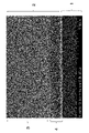
- Example 3 is an SEM image (Example 3) of a Cu surface to which the wet etching method of the present disclosure is applied.
- a pretreatment step in which a metal-containing film on a substrate is pretreated with a surface modification liquid containing an oxidizing substance to form an oxide film of the metal on the surface of the metal-containing film.
- an etching step is performed in which the metal-containing film having the oxide film of the metal is etched with an etching solution containing ⁇ -diketone in which a trifluoromethyl group and a carbonyl group are bonded.
- the metal-containing film to be etched by the wet etching method of the present disclosure contains a metal element capable of forming a complex with the ⁇ -diketone.
- a metal element capable of forming a complex with the ⁇ -diketone for example, as metal elements contained in the metal-containing film, Ti, Zr, Hf, V, Nb, Ta, Cr, Mo, W, Mn, Re, Fe, Ru, Os, Co, Rh, Ir, Ni, Pd, Pt. , Cu, Ag, Au, Zn, Cd, Al, Ga, In, Sn, Pb, and As.
- These metals can form a complex with ⁇ -diketone, form a complex with ⁇ -diketone in the etching solution, and dissolve in the etching solution.
- metal elements contained in the metal-containing film Ti, Zr, Hf, V, Cr, Mn, Fe, Ru, Os, Co, Rh, Ir, Ni, Pd, Pt, Cu, Zn, Al, Ga, In, Sn, Pb, and As are preferable, and Ti, Zr, Hf, Cr, Fe, Ru, Co, Ni, Pt, Cu, Zn, Al, Ga, In, Sn, and Pb are more preferable. In particular, Cu is preferable.
- the metal-containing film to be etched by the wet etching method of the present disclosure may be a combination of a plurality of types of metal-containing films.
- the metal-containing film is preferably a single film composed of one kind of metal element, a film of an alloy containing a plurality of metal elements, or a film of a compound containing a metal element. These films can be formed into films having a small surface roughness by sputtering, chemical vapor deposition (CVD), plating, or the like.
- the alloy film containing a plurality of metal elements is not only an alloy film such as NiCo, CoFe, CoPt, MnZn, NiZn, CuZn, FeNi, but also an alloy film doped with other elements such as CoFeB. May be good.
- the film of the compound containing the metal element examples include nitride films such as GaN and AlGaN, silicide films such as NiSi, CoSi and HfSi, arsenide films such as InAs, GaAs and InGaAs, and InP and GaP. Examples include a phosphide film. Further, in the metal-containing film containing a plurality of elements, the composition ratio of each element can be any value that can be produced.
- the substrate is not particularly limited as long as it is made of a material that can form a metal-containing film and does not react with the etching solution during wet etching.
- Silicon-based semiconductor material substrates such as silicon oxynitride and silicon carbide, and silicate glass material substrates such as soda lime glass, borosilicate glass, and quartz glass can be used.
- the substrate may have a film of a silicon-based semiconductor material or the like in addition to the metal-containing film.
- the surface modification liquid used in the pretreatment step is a liquid that can modify the outermost surface of the metal-containing film by coming into contact with the metal-containing film on the substrate.
- modification as used herein is an operation of rapidly advancing the complexion in the etching of the next step by changing the crystal grains and grain boundaries on the surface of the metal-containing film by a corrosive action by a chemical reaction.
- the metal may be oxidized by combining the metal on the outermost surface of the containing film with oxygen.
- the surface modification liquid of the present disclosure is a liquid capable of forming a layer of a metal oxide on the outermost surface of the metal-containing film by coming into contact with the metal-containing film on the substrate (referred to here).
- Oxide is an operation that increases the valence of a metal element by combining the metal with oxygen by a chemical reaction).
- the outermost surface of the metal-containing film can be formed into an oxide film of the metal having a certain thickness by pretreatment. Therefore, in the etching of the next step, the metal contained in the oxide film and the etching solution are contained. By forming a complex between the contained trifluoromethyl group and the ⁇ -diketone to which the carbonyl group is bonded and removing the oxide film, etching of a metal-containing film having a certain thickness on the substrate can be promoted. ..
- the removal of the oxide film formed on the outermost surface of the metal-containing film by the etching solution may be a part or all of the oxide film. Even when only a part of the oxide film is removed, the entire oxide film can be removed by repeating the etching process as shown in Examples described later.
- the etching solution and the complex are removed by rinsing the etching solution adhering to the substrate with PGMEA, IPA, ultrapure water, etc. immediately after removing the substrate from the etching solution, and then performing a drying operation with a gas blower or the like. Will be done. By performing this operation, further oxidation of the metal-containing film is suppressed, and the roughness of the metal surface after etching can be reduced.
- the surface modification liquid of the present disclosure contains an oxidizing substance.
- the oxidizing substance referred to here is not particularly limited as long as the surface modifying liquid containing the oxidizing substance can form an oxide on the outermost surface of the metal-containing film by contacting with the metal-containing film on the substrate.
- peroxides such as oxygen, ozone, hydrogen peroxide, dialkyl peroxide and urea hydrogen peroxide, oxidizing acids such as sulfuric acid, nitrate, permanganic acid and potassium permanganate or salts thereof, hexa Persulfonic acid such as fluoropropane persulfonic acid, methane persulfonic acid, trifluoromethane persulfonic acid, or p-toluene persulfonic acid or a salt thereof, peracetic acid, percarbonate such as sodium percarbonate or a salt thereof, ammonium persulfate, Persulfate or salts thereof such as sodium persulfate, tetramethylammonium persulfate, potassium persulfate and potassium peroxysulfate, sodium perchlorate, potassium perchlorate, ammonium perchlorate, tetramethylammonium perchlorate and the like.
- peroxides such as oxygen,
- Examples thereof include chloric acid or a salt thereof, periodic acid such as perioic acid, ammonium perioitate, or tetramethylammonium periodate or a salt thereof.
- periodic acid such as perioic acid, ammonium perioitate, or tetramethylammonium periodate or a salt thereof.
- oxygen, ozone, peroxides and oxidizing acids are preferable, and oxygen, ozone, hydrogen peroxide, nitric acid and sulfuric acid are particularly preferable.
- the surface modification liquid is prepared by diluting the above-mentioned oxidizing substance with a solvent.
- the solvent for diluting the oxidizing substance includes water, an organic solvent described later, or a mixture thereof, and any conventionally known solvent can be used as long as it dissolves the oxidizing substance.
- water is preferable as the main solvent to be diluted.
- the main solvent means that it contains 50% by weight or more with respect to 100 parts by weight of the diluted solvent.
- the content of the oxidizing substance is preferably 0.01 to 50% by mass, more preferably 0.02 to 20% by mass, and 0.05 to 10% by mass with respect to 100 parts by mass of the surface modification liquid. Especially preferable.
- the etching solution of the present disclosure is a solution containing a ⁇ -diketone in which a trifluoromethyl group and a carbonyl group are bonded, and an organic solvent.
- the complex with the metal is less likely to aggregate and the solid is less likely to precipitate.
- the organic solvent used in the etching solution is not particularly limited as long as it can dissolve the ⁇ -diketone and has little damage to the surface of the object to be treated, and a conventionally known organic solvent can be used.
- the organic solvent is preferably, for example, alcohol, hydrocarbon, ester, ether, ketone, halogen element-containing solvent, sulfoxide, lactone, carbonate, polyhydric alcohol derivative, nitrogen element-containing solvent, silicone, or a mixture thereof. used.
- hydrocarbons, esters, ethers, halogen element-containing solvents, polyhydric alcohol derivatives that do not have an OH group, or a mixed solution thereof can be used. It is preferable to use these because the stability of the etching solution is improved.
- Examples of the alcohol include methanol, ethanol, 1-propanol, 2-propanol, 1-butanol, 2-butanol, isobutanol, tert-butanol, 1-pentanol, 2-pentanol, 3-pentanol, 2 -Methyl-1-butanol, 3-methyl-1-butanol, 2-methyl-2-butanol, 3-methyl-2-butanol, 1-hexanol, 2-hexanol, 3-hexanol, 2-methyl-1-pen Tanol, 3-methyl-1-pentanol, 4-methyl-1-pentanol, 2-methyl-2-pentanol, 3-methyl-2-pentanol, 4-methyl-2-pentanol, 2-methyl -3-Pentanol, 3-Methyl-3-pentanol, 2,2-dimethyl-1-butanol, 3,3-dimethyl-1-butanol, 3,3-dimethyl-2-butano
- hydrocarbons examples include n-hexane, n-heptane, n-octane, n-nonane, n-decane, n-undecane, n-dodecane, n-tetradecane, n-hexadecane, n-octadecane, n-.
- Icosane as well as branched hydrocarbons corresponding to their carbon number (eg, isododecane, isosetan, etc.), cyclohexane, methylcyclohexane, decalin, benzene, toluene, xylene, (ortho-, meta-, or para-) diethylbenzene, There are 1,3,5-trimethylbenzene, naphthalene and the like.
- ester examples include ethyl acetate, n-propyl acetate, i-propyl acetate, n-butyl acetate, i-butyl acetate, n-pentyl acetate, i-pentyl acetate, n-hexyl acetate, n-heptyl acetate.
- ethers examples include di-n-propyl ether, ethyl-n-butyl ether, di-n-butyl ether, ethyl-n-amyl ether, di-n-amyl ether, ethyl-n-hexyl ether, and di-n.
- -Hexyl ethers di-n-octyl ethers, and ethers having branched hydrocarbon groups such as diisopropyl ethers and diisoamyl ethers corresponding to their carbon numbers, dimethyl ethers, diethyl ethers, methyl ethyl ethers, methylcyclopentyl ethers, There are diphenyl ether, tetrahydrofuran, dioxane, methyl perfluoropropyl ether, methyl perfluorobutyl ether, ethyl perfluorobutyl ether, methyl perfluorohexyl ether, ethyl perfluorohexyl ether and the like.
- ketone examples include acetone, acetylacetone, methylethylketone, methylpropylketone, methylbutylketone, 2-heptanone, 3-heptanone, cyclohexanone, isophorone and the like.
- halogen-containing element-containing solvent examples include perfluorocarbons such as perfluorooctane, perfluorononane, perfluorocyclopentane, perfluorocyclohexane, and hexafluorobenzene, 1, 1, 1, 3, 3-pentafluorobutane, and the like.
- Hydrofluorocarbons such as octafluorocyclopentane, 2,3-dihydrodecafluoropentane, Zeolola H (manufactured by Zeon Japan), methylperfluoroisobutyl ether, methylperfluorobutyl ether, ethylperfluorobutyl ether, ethylperfluoroisobutyl ether, Asahi Hydrofluoroethers such as Clean AE-3000 (manufactured by Asahi Glass), Novec7100, Novec7200, Novec7300, Novec7600 (all manufactured by 3M), chlorocarbons such as tetrachloromethane, hydrochlorocarbons such as chloroform, and chlorofluorocarbons such as dichlorodifluoromethane.
- Hydrofluorocarbons such as octafluorocyclopentane, 2,3-dihydrodecaflu
- Examples of the sulfoxide include dimethyl sulfoxide and the like.
- Examples of the lactones include ⁇ -propiolactone, ⁇ -butyrolactone, ⁇ -valerolactone, ⁇ -hexanolactone, ⁇ -heptanolactone, ⁇ -octanolactone, ⁇ -nonanolactone, ⁇ -decanolactone, ⁇ - Undecanolactone, ⁇ -dodecanolactone, ⁇ -valerolactone, ⁇ -hexanolactone, ⁇ -octanolactone, ⁇ -nonanolactone, ⁇ -decanolactone, ⁇ -undecanolactone, ⁇ -dodecanolactone, ⁇ -hexa There are nolactone and the like.
- Examples of the carbonate include dimethyl carbonate, ethylmethyl carbonate, diethyl carbonate, propylene carbonate and the like.
- polyvalent alcohol derivative examples include ethylene glycol monomethyl ether, ethylene glycol monoethyl ether, ethylene glycol monopropyl ether, ethylene glycol monobutyl ether, diethylene glycol monomethyl ether, diethylene glycol monoethyl ether, diethylene glycol monopropyl ether, and diethylene glycol monobutyl ether.
- nitrogen element-containing solvent examples include formamide, N, N-dimethylformamide, N, N-dimethylacetamide, N-diethylacetamide, N-methyl-2-pyrrolidone, N-ethyl-2-pyrrolidone, and N-propyl.
- -2-pyrrolidone 1,3-dimethyl-2-imidazolidinone, 1,3-diethyl-2-imidazolidinone, 1,3-diisopropyl-2-imidazolidinone, alkylamine, dialkylamine, trialkylamine , Ppyridine, etc.
- silicone examples include hexamethyldisiloxane, octamethyltrisiloxane, decamethyltetrasiloxane, dodecamethylpentasiloxane, and the like.
- the organic solvent preferably does not have an OH group of a hydrocarbon, an ester, an ether, a halogen element-containing solvent, a carbonate, or a polyhydric alcohol derivative from the viewpoint of stability of the etching solution.
- those having no OH group of esters, ethers and polyhydric alcohol derivatives are preferable, and propylene glycol monoalkyl ether acetate is preferable, and propylene glycol monomethyl ether acetate is particularly preferable, from the viewpoint of cost and environmental load.
- the water content in the etching solution is preferably 20% by mass or less, more preferably 10% by mass or less, based on 100 parts by mass of the etching solution. Further, it is more preferable, and particularly preferably 1% by mass or less.
- the concentration of ⁇ -diketone in the etching solution is preferably 0.5 to 15% by mass, more preferably 1 to 12% by mass, and further preferably 2 to 10% by mass. If the amount of ⁇ -diketone is too large, the etching solution becomes too expensive because ⁇ -diketone is generally more expensive than the organic solvent. Further, if it is more than 10% by mass, the roughness tends to deteriorate. On the other hand, if the ⁇ -diketone is less than 1% by mass, the etching tends not to proceed.
- the etching solution contains additives such as citric acid, formic acid, acetic acid and trifluoroacetic acid for the purpose of improving the etching rate and improving the etching selectivity as long as the object to be treated is not adversely affected. May include.
- the amount of the additive added is adjusted within a range that does not adversely affect the object to be treated, and is, for example, 0.01 to 20% by mass, 0.1 to 15% by mass, and further 0.5 by mass with respect to the etching solution. It may be added in the range of ⁇ 10% by mass.
- the etching solution may be substantially composed of a ⁇ -diketone in which a trifluoromethyl group and a carbonyl group are bonded, and an organic solvent.
- the wet etching method of the present disclosure includes a first step of bringing the surface modification liquid into contact with the metal-containing film and a second step of bringing the etching solution into contact with the metal-containing film modified by the surface modification liquid.
- etching can be performed without increasing the roughness of the metal-containing film.
- a surface modification liquid and / or an etching liquid is put into an apparatus such as an etching apparatus in which a processing object having a metal-containing film is arranged on a substrate, so that the surface modification liquid and / or the surface modification liquid and /
- the metal-containing film may be wet-etched by bringing the etching solution into contact with the metal-containing film of the object to be treated.
- the apparatus and method for applying the wet etching solution of the present disclosure are not particularly limited.
- a batch method using a processing device can be mentioned.
- the form of the etching solution when supplying the etching solution in a liquid state to the surface of the object to be treated is not particularly limited as long as it becomes a liquid when it is held by the object to be processed, and for example, a liquid. There is steam and so on.
- the first step and the second step do not have to be continuous. It is preferable to provide a cleaning step between the first step and the second step to rinse the surface of the metal-containing film to which the surface modification liquid is attached. By providing the cleaning step, the content of the oxidizing substance contained in the etching solution can be reduced, and further, it is possible to avoid contact with the metal-containing film.
- An example of the cleaning step is to bring water, an organic solvent, or the like into contact with the metal-containing membrane to remove the oxidizing substance from the metal-containing membrane.
- the organic solvent used in the cleaning step is not particularly limited as long as it can dissolve the etching solution and / or the oxidizing substance, and conventionally known organic solvents can be used, for example. Examples of the organic solvent used in the etching solution can be used. Further, from the viewpoint of solubility of the surface modification liquid, water, alcohol and polyhydric alcohol derivatives are preferable. Further, it is preferable to use a solvent of the surface modification liquid. Further, in the washing step, water or an organic solvent may be used for rinsing a plurality of times.
- the solvent of the surface modification liquid and the solvent of the etching solution are incompatible, it is preferable to rinse with a solvent that dissolves in both, and for example, as shown in Examples described later, contact with the surface modification liquid. Later, rinsing with ultrapure water, 2-propanol, propylene glycol-1-monomethyl ether-2-acetate, and then contacting with an etching solution is one of the preferred embodiments.
- the first step and the second step may be repeated.
- the etching amount can be increased without deteriorating the roughness of the surface.
- the substrate taken out after contact with the etching solution is subjected to ultrapropylene glycol-1-monomethylether-2-acetylate, 2-propanol, or ultrapure water. Rinsing with or the like and then contacting with the surface modifier is one of the preferred embodiments.
- the oxidizing substance contained in the etching solution in the present disclosure is preferably 0.01% by mass or less, preferably 0.005% by mass or less, based on 100 parts by mass of the etching solution. Within this range, it is not always necessary to provide a cleaning step between the first step and the second step and rinse the surface of the metal-containing film to which the surface modifying liquid is attached. By rinsing and adjusting the amount of the oxidizing substance to 0.001% by mass or less, it becomes possible to minimize the roughness of the metal surface after etching.
- the detection limit may be the lower limit for the content of oxidizing substances. Further, the lower limit may be 0.0001% by mass, and the rinsing may be repeated so as to be 0.0001% by mass or more and 0.001% by mass or less.
- a step of bringing an etching solution capable of etching the metal-containing film into contact with the metal-containing film may be carried out.
- the outermost surface of the metal-containing film may be naturally oxidized due to the process before the treatment with the surface modifier or the influence of atmospheric contact. It is preferable to carry out the step of contacting with the etching solution first because the natural oxide on the outermost surface can be removed.
- the etching solution here, the etching solution used in the second step may be applied.
- the temperature of the surface modification liquid is not particularly limited as long as the surface modification liquid can maintain a liquid state, but the length of time for contacting the surface modification liquid and the metal after etching are not particularly limited. Considering the roughness of the contained film, it can be appropriately set at about ⁇ 10 to 60 ° C.
- the temperature of the etching solution is not particularly limited as long as the etching solution can be kept in a liquid state, but is -10 to 10 in consideration of the length of time for contacting the etching solution and the roughness of the metal-containing film after etching. It can be appropriately set at about 100 ° C.
- the length of contact with the surface modifier is not particularly limited, but is preferably 60 minutes or less, more preferably 10 minutes or less, and particularly preferably 2 minutes or less in consideration of the efficiency of the semiconductor device manufacturing process.
- the length of contact with the etching solution is not particularly limited, but is preferably 60 minutes or less, more preferably 10 minutes or less, and particularly preferably 2 minutes or less in consideration of the efficiency of the semiconductor device manufacturing process.
- the length of time for contact with the surface modification liquid or the etching liquid is, for example, the time for discharging the liquid to the substrate to be treated, the time for immersing the substrate, or the time when the substrate is installed. It refers to the time until the etching solution is introduced into the inside of the process chamber and then the etching solution in the process chamber is discharged in order to finish the etching process.
- the wet etching method according to the present disclosure enables the manufacture of high-performance devices.
- the device according to the present disclosure can be inexpensively manufactured by using a metal-containing film etched by the wet etching method according to the present disclosure.
- Such devices include, for example, solar cells, hard disk drives, lock ICs, microprocessors, dynamic random access memory, phase change memory, ferroelectric memory, magnetoresistive memory, resistance change memory, MEMS and the like. Can be mentioned.
- Ra (nm) was determined, and the Ra difference ( ⁇ Ra) before and after the etching treatment was determined.
- Ra is a three-dimensional extension of the average roughness of the center line defined in JIS B 0601 applied to the measurement surface, and "the absolute value of the deviation from the reference surface to the designated surface is averaged. It was calculated by the following formula as "value”.
- X L , X R , Y B , and Y T indicate the measurement range of the X coordinate and the Y coordinate, respectively.
- S 0 is the area when the measurement surface is ideally flat, and is a value of (X R ⁇ XL ) ⁇ (Y B ⁇ Y T ).
- F (X, Y) represents the height at the measurement point (X, Y), and Z 0 represents the average height in the measurement plane.
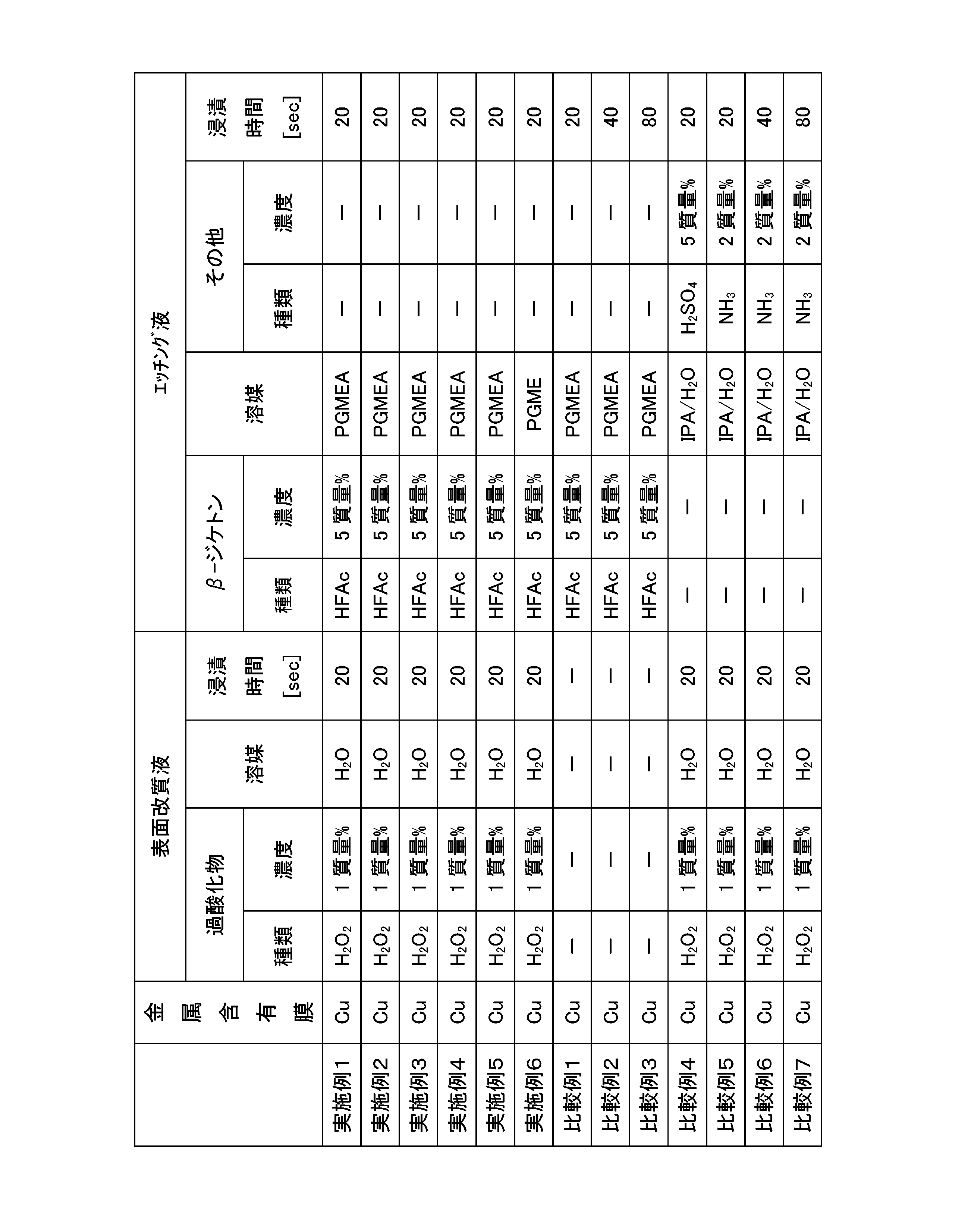
- Example 1 (Preparation of solution) A surface modifier was prepared by mixing hydrogen peroxide solution and ultrapure water ( H2O ) so that the hydrogen peroxide concentration was 1% by mass. Hexafluoroacetylacetone (HFAc) and propylene glycol-1-monomethyl ether-2-acetate (PGMEA) as a solvent were mixed so that HFAc was 5% by mass to prepare an etching solution. The water content in the etching solution was 1% by mass or less.
- HFAc Hexafluoroacetylacetone
- PGMEA propylene glycol-1-monomethyl ether-2-acetate
- the water content in the etching solution was 1% by mass or less.
- Examples 2 to 4 A surface modification liquid and an etching liquid were prepared in the same manner as in Example 1. Using the same silicon substrate as in Example 1, a series of operations of pretreatment step ⁇ rinsing ⁇ etching step ⁇ rinsing was repeated 2, 5 and 10 times, and finally the surface was dried with a gas blower for 10 seconds. , The wet etching treatment was performed in the same manner as in Example 1.
- Example 5 A surface modification liquid and an etching liquid were prepared in the same manner as in Example 1. Before immersing in the surface modifier, the same silicon substrate as in Example 1 was immersed in the etching solution at 24 ° C. for 20 seconds, and then the etching solution adhering to the substrate surface was rinsed. The rinse was immersed in PGMEA, IPA, and ultrapure water at 24 ° C. for 20 seconds each. Then, the wet etching treatment was performed by the same method as in Example 1.
- Example 6 A surface modifier was prepared in the same manner as in Example 1. Further, an etching solution was prepared in the same manner as in Example 1 except that propylene glycol monomethyl ether (PGME) was used as a solvent.
- PGME propylene glycol monomethyl ether
- the same silicon substrate as in Example 1 was immersed in the surface modifier at 24 ° C. for 20 seconds. Then, the surface modifier adhering to the substrate surface was immersed in the etching solution at 24 ° C. for 20 seconds with the surface modifier adhering to the surface without rinsing. This operation was repeated 10 times, and then the etching solution adhering to the substrate surface was rinsed. The rinse was immersed in PGME, IPA, and ultrapure water at 24 ° C.
- PGME propylene glycol monomethyl ether
- the surface modification liquid is slightly dissolved in the etching solution, and 0.003% by mass of hydrogen peroxide is added to the total amount of the etching solution and the dissolved surface modification solution. It was blended in.
- Example 1 An etching solution was prepared in the same manner as in Example 1. The same silicon substrate as in Example 1 was immersed in an etching solution at 24 ° C. for 20 seconds, then immersed in PGMEA and 2-propanol (IPA) at 24 ° C. for 20 seconds, and finally with a gas blower for 10 seconds. The wet etching treatment was performed in the same manner as in Example 1 except that the surface was dried. That is, in this comparative example, the treatment was performed by a method of omitting the pretreatment step of immersing in the surface modification liquid.
- IPA 2-propanol
- Comparative Example 2 In the etching step, the wet etching treatment was performed in the same manner as in Comparative Example 1 except that the etching solution was immersed in the etching solution at 24 ° C. for 40 seconds.
- Example 4 The wet etching treatment was carried out in the same manner as in Example 1 except that an etching solution prepared by mixing 98% sulfuric acid and IPA so that the sulfuric acid content was 5% by mass was used.
- FIG. 1 is an SEM image of the Cu surface after performing the etching treatment of Example 3 five times. The Cu surface after etching was smooth, and no large roughness was observed.
- Example 1 to 5 the surface roughness after etching is larger than that of the Cu film surface before the surface modifier is brought into contact with the metal-containing film and the Cu oxide film surface before the etching treatment. Although there was no change, the results of Examples 1 to 5 in which the surface modification liquid was removed by rinsing had a smaller surface roughness after etching than in Example 6 in which the surface modification liquid was not removed by rinsing. It became.
Landscapes
- Chemical & Material Sciences (AREA)
- Chemical Kinetics & Catalysis (AREA)
- General Chemical & Material Sciences (AREA)
- Engineering & Computer Science (AREA)
- Materials Engineering (AREA)
- Mechanical Engineering (AREA)
- Metallurgy (AREA)
- Organic Chemistry (AREA)
- ing And Chemical Polishing (AREA)
- Weting (AREA)
Abstract
Description
本開示のウェットエッチング方法では、基板上の金属含有膜を、酸化性物質を含む表面改質液で前処理して前記金属含有膜の表面に前記金属の酸化膜を形成する前処理工程(第1工程)後に、トリフルオロメチル基とカルボニル基が結合したβ-ジケトンを含むエッチング液を用いて前記金属の酸化膜を有する前記金属含有膜をエッチングするエッチング工程(第2工程)を行う。
また、エッチング液の温度は、エッチング液が液体状態を保てる温度であれば特に限定されないが、エッチング液を接触させる時間の長さと、エッチング後の金属含有膜のラフネスを考慮して、-10~100℃程度で適宜設定することができる。
また、エッチング液に接触させる時間の長さは特に制限されるものではないが、半導体デバイス製造プロセスの効率を考慮すると、60分以内、さらに10分以内、特に2分以内であることが好ましい。ここで、表面改質液やエッチング液に接触させる時間の長さとは、例えば、処理対象物である基板に液を吐出している時間や、基板を浸漬している時間や、基板が設置されているプロセスチャンバーの内部にエッチング液を導入し、その後、エッチング処理を終える為に該プロセスチャンバーの内のエッチング液を排出するまでの時間を指す。
また、本開示のウェットエッチング方法を用いると、ドライエッチング装置に比べて安価なウェットエッチング装置を使用して、金属含有膜のエッチング後のラフネスを改善することができるため、半導体デバイスの品質を向上することができる。
本開示に係るウェットエッチング方法により、高性能のデバイスの製造が可能である。本開示に係るデバイスは、本開示に係るウェットエッチング方法によりエッチングした金属含有膜を用いることにより、安価に製造することができる。このようなデバイスとして、例えば、太陽電池、ハードディスクドライブ、ロックIC、マイクロプロセッサ、ダイナミック・ランダム・アクセス・メモリ、相変化型メモリ、強誘電体メモリ、磁気抵抗メモリ、抵抗変化型メモリ、MEMS等を挙げることができる。
(エッチング量の測定)
エッチング量は、エッチング液に浸漬前後の基板の質量変化から算出した。この際、金属含有膜として用いたCuの比重は8.94g/cm3とした。エッチング速度はエッチング量[nm}/浸漬時間[sec]によって求められる。
(表面粗さの測定)
エッチング前(初期状態)の金属含有膜の表面と、エッチング後の表面、それぞれをAFM(SHIMADZU SPM-9700:走査範囲1.00μm、走査速度1.0Hz)で測定し、中心線平均面粗さRa(nm)を求め、エッチング処理の前後のRa差(ΔRa)を求めた。なお、Raは、JIS B 0601で定義されている中心線平均粗さを測定面に対し適用して三次元に拡張したものであり、「基準面から指定面までの偏差の絶対値を平均した値」として次式で算出した。

(表面形状の観察)
表面形状をSEM(日立製SU8010:加速電圧10.0KV、エッミッション20μA)で観察した。
(溶液の調製)
過酸化水素水と超純水(H2O)を用いて、過酸化水素濃度が1質量%となるように混合させ、表面改質液を調製した。ヘキサフルオロアセチルアセトン(HFAc)、溶媒としてプロピレングリコール-1-モノメチルエーテル-2-アセタート(PGMEA)を用いて、HFAcが5質量%となるように混合させ、エッチング液を調製した。なお、エッチング液中の水分は1質量%以下であった。
(ウェットエッチング処理)
金属含有膜としてメッキ法にて製膜されたCu膜(厚さ1μm、中心線平均面粗さRa=6nm)を有するシリコン基板を処理対象とした。この基板を、前記で得られた表面改質液に24℃で20秒間浸漬させて前処理工程を行うことにより、Cuの最表面に酸化物膜が形成された。その後、基板表面に付着した表面改質液をリンスして除去した。リンスは、超純水、2-プロパノール(IPA)、PGMEAに、それぞれ24℃で20秒間浸漬させた。次に、前記で得られたエッチング液に24℃で20秒間基板を浸漬させてエッチング工程を行った。その後、基板表面に付着したエッチング液をリンスした。リンスは、PGMEA、IPA、超純水に、それぞれ24℃で20秒間浸漬させた。最後に、ガスブロワーで10秒間表面を乾燥させた。
実施例1と同様に表面改質液とエッチング液を調製した。実施例1と同じシリコン基板を処理対象として用い、前処理工程→リンス→エッチング工程→リンスの一連の操作を2、5、10回繰り返し、最後にガスブロワーで10秒間表面を乾燥させた以外は、実施例1と同様の方法でウェットエッチング処理を行った。
実施例1と同様に表面改質液とエッチング液を調製した。表面改質液に浸漬する前に、実施例1と同じシリコン基板を、エッチング液に24℃で20秒間浸漬させた後、基板表面に付着したエッチング液をリンスした。リンスは、PGMEA、IPA、超純水に、それぞれ24℃で20秒間浸漬させた。その後、実施例1と同様の方法でウェットエッチング処理を行った。
実施例1と同様に表面改質液を調製した。また、溶媒としてプロピレングリコールモノメチルエーテル(PGME)を用いたこと以外は実施例1と同様にエッチング液を調製した。ウェットエッチング処理において、実施例1と同じシリコン基板を、表面改質液に24℃で20秒間浸漬させた。その後、基板表面に付着した表面改質液をリンスせずに表面改質液が付着した状態でエッチング液に24℃で20秒間浸漬させた。この操作を10回繰り返し、その後、基板表面に付着したエッチング液をリンスした。リンスは、PGME、IPA、超純水に、それぞれ24℃で20秒間浸漬させた。最後に、ガスブロワーで10秒間表面を乾燥させた。すなわち、本実施例では、エッチング液に該表面改質液がわずかに溶け込む形となっており、エッチング液と溶け込んだ表面改質液の総量に対して、0.003質量%の過酸化水素が溶け込んでいた。
実施例1と同様にエッチング液を調製した。前記実施例1と同じシリコン基板を、エッチング液に24℃で20秒間浸漬させ、その後、PGMEA、2-プロパノール(IPA)に、それぞれ24℃で20秒間浸漬させて、最後にガスブロワーで10秒間表面を乾燥させた以外は、実施例1と同様の方法でウェットエッチング処理を行った。すなわち、本比較例では、表面改質液に浸漬する前処理工程を省略する方法で処理を行った。
エッチング工程において、エッチング液に24℃で40秒間浸漬させた以外は、比較例1と同様の方法でウェットエッチング処理を行った。
エッチング工程において、エッチング液に24℃で80秒間浸漬させた以外は、比較例1と同様の方法でウェットエッチング処理を行った。
98%硫酸とIPAを用いて、硫酸が5質量%となるように混合させて調製したエッチング液を用いた以外は、実施例1と同様の方法でウェットエッチング処理を行った。
25%アンモニア水とIPAを用いて、NH3が2質量%となるように混合させ、エッチング液を調製した以外は、実施例1と同様の方法でウェットエッチング処理を行った。
エッチング工程において、エッチング液に24℃で40秒間浸漬させた以外は、比較例5と同様の方法でウェットエッチング処理を行った。
エッチング工程において、エッチング液に24℃で80秒間浸漬させた以外は、比較例5と同様の方法でウェットエッチング処理を行った。
結果は、表1~2の実施例1~6、比較例1~3に示すとおり、本発明のエッチング方法は、所定の金属元素を含む金属含有膜のエッチングにおけるエッチング速度の向上とΔRaの増大の抑制が可能であった。また、エッチング処理の繰り返し回数に応じてエッチング量を増加させることができ、エッチング量が増加してもΔRaの増大の抑制ができた。エッチング液にβ-ジケトンを使用せずに、酸や塩基を用いた比較例4~7ではΔRaが著しく増大した。
図1は、実施例3のエッチング処理を5回実行した後のCu表面のSEM画像であり、エッチング後のCu表面は平滑であり、大きなラフネスも見られなかった。

2: 金属含有膜
3: 金属含有膜の表面(=ラフネスの面)
4: 金属含有膜の断面
Claims (10)
- 基板上の金属含有膜を、表面改質液で前処理し、次いでエッチング液を用いてエッチングするウェットエッチング方法であって、
前記エッチング液が、トリフルオロメチル基とカルボニル基が結合したβ-ジケトンと、有機溶媒を含む溶液であり、
前記金属含有膜が、前記β-ジケトンと錯体を形成可能な金属元素を含み、
前記表面改質液が前記金属元素に対する酸化性物質を含み、
前記表面改質液を前記金属含有膜に接触させて前記金属含有膜の表面に前記金属元素の酸化膜を形成する第一工程と、
前記エッチング液を、前記酸化膜を有する前記金属含有膜に接触させる第二工程と、を含む、ウェットエッチング方法。 - 前記第二工程において、前記酸化性物質を前記金属含有膜に接触させない、請求項1に記載のウェットエッチング方法。
- 前記第一工程と、第二工程との間に基板表面の洗浄工程を含む、請求項1又は2に記載のウェットエッチング方法。
- 前記表面改質液に前記金属含有膜を接触させる時間が2分以内であり、前記エッチング液を、前記酸化膜を有する前記金属含有膜に接触させる時間が2分以内である、請求項1~3のいずれか1項に記載のウェットエッチング方法。
- 前記エッチング液中のβ-ジケトンの濃度が0.5~15質量%であることを特徴とする請求項1~4のいずれか1項に記載のウェットエッチング方法。
- 前記エッチング液中は、エッチング液100質量部に対して0.01質量%以上の酸化性物質を含まない、請求項1~5のいずれか1項に記載のウェットエッチング方法。
- 前記酸化性物質が、酸素、オゾン、過酸化物、酸化性の酸又はその塩、過スルホン酸又はその塩、過炭酸又はその塩、過硫酸又はその塩、過塩素酸又はその塩、及び過ヨウ素酸又はその塩からなる群より選ばれる少なくとも1種であることを特徴とする請求項1~6のいずれか1項に記載のウェットエッチング方法。
- 前記酸化性物質が、酸素、オゾン、過酸化水素、硝酸、及び硫酸からなる群より選ばれる少なくとも1種であることを特徴とする請求項1~7のいずれか1項に記載のウェットエッチング方法。
- 前記表面改質液が、表面改質液100重量部に対して0.01質量%~20質量%の酸化性物質を含むことを特徴とする請求項1~8のいずれか1項に記載のウェットエッチング方法。
- 前記基板の材料が、シリコン系半導体材料又はケイ酸塩ガラス材料であることを特徴とする請求項1~9のいずれか1項に記載のウェットエッチング方法。
Priority Applications (4)
| Application Number | Priority Date | Filing Date | Title |
|---|---|---|---|
| JP2022556950A JP7791441B2 (ja) | 2020-10-16 | 2021-10-11 | ウェットエッチング方法 |
| KR1020237015045A KR20230079204A (ko) | 2020-10-16 | 2021-10-11 | 웨트 에칭 방법 |
| US18/030,404 US20230374669A1 (en) | 2020-10-16 | 2021-10-11 | Wet Etching Method |
| CN202180070131.5A CN116324036A (zh) | 2020-10-16 | 2021-10-11 | 湿式蚀刻方法 |
Applications Claiming Priority (2)
| Application Number | Priority Date | Filing Date | Title |
|---|---|---|---|
| JP2020-174486 | 2020-10-16 | ||
| JP2020174486 | 2020-10-16 |
Publications (1)
| Publication Number | Publication Date |
|---|---|
| WO2022080288A1 true WO2022080288A1 (ja) | 2022-04-21 |
Family
ID=81208168
Family Applications (1)
| Application Number | Title | Priority Date | Filing Date |
|---|---|---|---|
| PCT/JP2021/037501 Ceased WO2022080288A1 (ja) | 2020-10-16 | 2021-10-11 | ウェットエッチング方法 |
Country Status (6)
| Country | Link |
|---|---|
| US (1) | US20230374669A1 (ja) |
| JP (1) | JP7791441B2 (ja) |
| KR (1) | KR20230079204A (ja) |
| CN (1) | CN116324036A (ja) |
| TW (1) | TW202229645A (ja) |
| WO (1) | WO2022080288A1 (ja) |
Families Citing this family (1)
| Publication number | Priority date | Publication date | Assignee | Title |
|---|---|---|---|---|
| CN120248894B (zh) * | 2025-02-24 | 2026-03-17 | 安瑞森(宿迁)电子材料有限公司 | 一种液晶面板用双氧水系蚀刻液及其制备方法 |
Citations (3)
| Publication number | Priority date | Publication date | Assignee | Title |
|---|---|---|---|---|
| JPH11140652A (ja) * | 1997-11-06 | 1999-05-25 | Anelva Corp | 成膜処理装置内の付着金属膜のクリーニング方法 |
| JP2017028257A (ja) * | 2015-07-23 | 2017-02-02 | セントラル硝子株式会社 | ウェットエッチング方法及びエッチング液 |
| JP2017028198A (ja) * | 2015-07-27 | 2017-02-02 | 東京エレクトロン株式会社 | エッチング方法及びエッチング装置 |
Family Cites Families (8)
| Publication number | Priority date | Publication date | Assignee | Title |
|---|---|---|---|---|
| JP3907151B2 (ja) | 2000-01-25 | 2007-04-18 | 株式会社東芝 | 半導体装置の製造方法 |
| US7122484B2 (en) * | 2004-04-28 | 2006-10-17 | Taiwan Semiconductor Manufacturing Company, Ltd. | Process for removing organic materials during formation of a metal interconnect |
| WO2007120259A2 (en) * | 2005-11-08 | 2007-10-25 | Advanced Technology Materials, Inc. | Formulations for removing copper-containing post-etch residue from microelectronic devices |
| JP5396514B2 (ja) | 2011-06-30 | 2014-01-22 | 富士フイルム株式会社 | エッチング方法及びこれに用いられるエッチング液、これを用いた半導体基板製品の製造方法 |
| JP5601286B2 (ja) * | 2011-07-25 | 2014-10-08 | 信越化学工業株式会社 | レジスト材料及びこれを用いたパターン形成方法 |
| JP6261926B2 (ja) * | 2013-09-18 | 2018-01-17 | 関東化學株式会社 | 金属酸化物エッチング液組成物およびエッチング方法 |
| JP7611857B2 (ja) * | 2019-05-01 | 2025-01-10 | フジフイルム エレクトロニック マテリアルズ ユー.エス.エー., インコーポレイテッド | エッチング組成物 |
| JP7050184B2 (ja) * | 2019-09-27 | 2022-04-07 | 株式会社トクヤマ | ルテニウムの半導体用処理液及びその製造方法 |
-
2021
- 2021-10-11 WO PCT/JP2021/037501 patent/WO2022080288A1/ja not_active Ceased
- 2021-10-11 US US18/030,404 patent/US20230374669A1/en not_active Abandoned
- 2021-10-11 CN CN202180070131.5A patent/CN116324036A/zh active Pending
- 2021-10-11 KR KR1020237015045A patent/KR20230079204A/ko not_active Ceased
- 2021-10-11 JP JP2022556950A patent/JP7791441B2/ja active Active
- 2021-10-15 TW TW110138317A patent/TW202229645A/zh unknown
Patent Citations (3)
| Publication number | Priority date | Publication date | Assignee | Title |
|---|---|---|---|---|
| JPH11140652A (ja) * | 1997-11-06 | 1999-05-25 | Anelva Corp | 成膜処理装置内の付着金属膜のクリーニング方法 |
| JP2017028257A (ja) * | 2015-07-23 | 2017-02-02 | セントラル硝子株式会社 | ウェットエッチング方法及びエッチング液 |
| JP2017028198A (ja) * | 2015-07-27 | 2017-02-02 | 東京エレクトロン株式会社 | エッチング方法及びエッチング装置 |
Also Published As
| Publication number | Publication date |
|---|---|
| JP7791441B2 (ja) | 2025-12-24 |
| US20230374669A1 (en) | 2023-11-23 |
| JPWO2022080288A1 (ja) | 2022-04-21 |
| KR20230079204A (ko) | 2023-06-05 |
| TW202229645A (zh) | 2022-08-01 |
| CN116324036A (zh) | 2023-06-23 |
Similar Documents
| Publication | Publication Date | Title |
|---|---|---|
| TWI572746B (zh) | 用以移除蝕刻後殘餘物之液體清洗劑 | |
| EP3602606B1 (en) | Surface treatment methods and compositions therefor | |
| JP5442436B2 (ja) | 表面上の残留物を除去するための洗浄調合物 | |
| CN107533971B (zh) | 湿式蚀刻方法和蚀刻液 | |
| TWI838332B (zh) | 用於移除半導體基材上的殘餘物之清潔調配物 | |
| US7011716B2 (en) | Compositions and methods for drying patterned wafers during manufacture of integrated circuitry products | |
| KR102490840B1 (ko) | 반도체 기판상의 잔류물을 제거하기 위한 세정 조성물 | |
| US20020119245A1 (en) | Method for etching electronic components containing tantalum | |
| KR102375342B1 (ko) | Tin 풀-백 및 클리닝 조성물 | |
| JP2023133294A (ja) | 洗浄用組成物 | |
| JP7791441B2 (ja) | ウェットエッチング方法 | |
| TW202235683A (zh) | 濕式蝕刻溶液及濕式蝕刻方法 | |
| KR101630654B1 (ko) | 에칭방법, 이것을 사용한 반도체 기판 제품 및 반도체 소자의 제조방법 | |
| US6173720B1 (en) | Process for treating a semiconductor substrate | |
| JPH0959685A (ja) | 半導体装置の洗浄に使用される洗浄液及びこれを用いた洗浄方法 | |
| US11898123B2 (en) | Cleaning compositions | |
| TWI921371B (zh) | 清潔組成物,自半導體基板清潔殘餘物之方法及處理在表面上具有金屬層之半導體基板的方法 | |
| JP4396267B2 (ja) | エッチング剤 |
Legal Events
| Date | Code | Title | Description |
|---|---|---|---|
| 121 | Ep: the epo has been informed by wipo that ep was designated in this application |
Ref document number: 21880027 Country of ref document: EP Kind code of ref document: A1 |
|
| ENP | Entry into the national phase |
Ref document number: 2022556950 Country of ref document: JP Kind code of ref document: A |
|
| ENP | Entry into the national phase |
Ref document number: 20237015045 Country of ref document: KR Kind code of ref document: A |
|
| NENP | Non-entry into the national phase |
Ref country code: DE |
|
| 122 | Ep: pct application non-entry in european phase |
Ref document number: 21880027 Country of ref document: EP Kind code of ref document: A1 |