WO2022080148A1 - フィルムコンデンサ - Google Patents
フィルムコンデンサ Download PDFInfo
- Publication number
- WO2022080148A1 WO2022080148A1 PCT/JP2021/036246 JP2021036246W WO2022080148A1 WO 2022080148 A1 WO2022080148 A1 WO 2022080148A1 JP 2021036246 W JP2021036246 W JP 2021036246W WO 2022080148 A1 WO2022080148 A1 WO 2022080148A1
- Authority
- WO
- WIPO (PCT)
- Prior art keywords
- dielectric film
- film
- metal layer
- main surface
- external electrode
- Prior art date
- Legal status (The legal status is an assumption and is not a legal conclusion. Google has not performed a legal analysis and makes no representation as to the accuracy of the status listed.)
- Ceased
Links
Images


Classifications
-
- H—ELECTRICITY
- H01—ELECTRIC ELEMENTS
- H01G—CAPACITORS; CAPACITORS, RECTIFIERS, DETECTORS, SWITCHING DEVICES, LIGHT-SENSITIVE OR TEMPERATURE-SENSITIVE DEVICES OF THE ELECTROLYTIC TYPE
- H01G4/00—Fixed capacitors; Processes of their manufacture
- H01G4/32—Wound capacitors
-
- H—ELECTRICITY
- H01—ELECTRIC ELEMENTS
- H01G—CAPACITORS; CAPACITORS, RECTIFIERS, DETECTORS, SWITCHING DEVICES, LIGHT-SENSITIVE OR TEMPERATURE-SENSITIVE DEVICES OF THE ELECTROLYTIC TYPE
- H01G4/00—Fixed capacitors; Processes of their manufacture
- H01G4/002—Details
- H01G4/018—Dielectrics
-
- H—ELECTRICITY
- H01—ELECTRIC ELEMENTS
- H01G—CAPACITORS; CAPACITORS, RECTIFIERS, DETECTORS, SWITCHING DEVICES, LIGHT-SENSITIVE OR TEMPERATURE-SENSITIVE DEVICES OF THE ELECTROLYTIC TYPE
- H01G4/00—Fixed capacitors; Processes of their manufacture
- H01G4/002—Details
- H01G4/018—Dielectrics
- H01G4/06—Solid dielectrics
- H01G4/14—Organic dielectrics
- H01G4/18—Organic dielectrics of synthetic material, e.g. derivatives of cellulose
-
- H—ELECTRICITY
- H01—ELECTRIC ELEMENTS
- H01G—CAPACITORS; CAPACITORS, RECTIFIERS, DETECTORS, SWITCHING DEVICES, LIGHT-SENSITIVE OR TEMPERATURE-SENSITIVE DEVICES OF THE ELECTROLYTIC TYPE
- H01G4/00—Fixed capacitors; Processes of their manufacture
- H01G4/002—Details
- H01G4/005—Electrodes
- H01G4/015—Special provisions for self-healing
Definitions
- the present invention relates to a film capacitor.
- a film capacitor having a structure in which a first metal layer and a second metal layer facing each other across the film are arranged while using a flexible film as a dielectric film is known.
- a film on which a first metal layer is formed and a film on which a second metal layer is formed are wound or laminated to form a laminated body, and then on both end faces of the laminated body.
- Manufactured by forming an external electrode for example, a film on which a first metal layer is formed and a film on which a second metal layer is formed are wound or laminated to form a laminated body, and then on both end faces of the laminated body.
- Patent Document 1 includes a metallized film formed by superimposing a first film member having a metal film formed on at least one surface thereof and a second film member, and the metallized film is wound.
- the first protruding end and the first immersive end are configured to be repeated in the stacking direction, and the metal film is formed from the first immersive end of the first protruding end.
- a film capacitor is disclosed that is configured to be exposed at a portion protruding in the width direction.
- a film capacitor as described in Patent Document 1 is not supposed to be used so as to repeat a low temperature state and a high temperature state, and when used so as to repeat a low temperature state and a high temperature state, Repeat contraction and expansion. As described above, when the film capacitor repeatedly contracts and expands, stress is repeatedly generated on the external electrode, which causes a problem that the equivalent series resistance of the film capacitor increases.
- the present invention has been made to solve the above problems, and an object of the present invention is to provide a film capacitor in which an increase in equivalent series resistance is suppressed even when it is used to repeat a low temperature state and a high temperature state. It is something to do.
- the film capacitor of the present invention includes a first dielectric film, a second dielectric film, a first metal layer, and a second metal layer, and has a first end face and a second end face facing each other in the width direction.
- the first dielectric film comprises a body, a first external electrode connected to the first end surface of the laminate, and a second external electrode connected to the second end surface of the laminate.
- the second dielectric film has a first main surface and a second main surface facing in a thickness direction orthogonal to the width direction, and the second dielectric film has a third main surface and a fourth main surface facing in the thickness direction.
- the first main surface of the first dielectric film and the fourth main surface of the second dielectric film face each other in the thickness direction, and the first dielectric film is described.
- the second main surface and the third main surface of the second dielectric film face each other in the thickness direction, and the first metal layer is provided on the first main surface of the first dielectric film.
- the second metal layer is connected to the first external electrode and is not connected to the second external electrode, and the second metal layer is the first main surface of the first dielectric film and the first dielectric film.
- the second main surface of the above, or the third main surface of the second dielectric film, which is provided on one of the main surfaces, is connected to the second external electrode, and is connected to the first external electrode.
- the dielectric film in which the first metal layer is provided on the main surface has the first metal layer.
- the first end surface of the laminated body has the above.
- the first unevenness whose contour line is a curve connecting the ends of the dielectric film provided on the main surface of the first metal layer is continuously present in the thickness direction, and conforms to JIS B 0601: 2001.
- the first unevenness has a height of 0.07 mm or more and 0.25 mm or less, an interval of 0.07 mm or more and 0.15 mm or less, and the first metal layer in the width direction.
- the second metal layer is provided on the main surface of the dielectric film in which the second metal layer is provided on the main surface.
- the second metal layer is mainly formed on the second end surface of the laminated body.
- the second unevenness whose contour line is a curve connecting the ends of the dielectric films provided on the surface exists continuously in the thickness direction and is measured in accordance with JIS B 0601: 2001.
- the second unevenness has a height of 0.07 mm or more and 0.25 mm or less, an interval of 0.07 mm or more and 0.15 mm or less, and the second metal layer is provided on the main surface in the width direction.
- a second gap exists between the uncoated dielectric film and the second external electrode, and the length of the second gap in the width direction is 0.3 mm or more. ..
- the present invention it is possible to provide a film capacitor in which an increase in equivalent series resistance is suppressed even when it is used so as to repeat a low temperature state and a high temperature state.
- FIG. 3 It is a perspective schematic diagram which shows an example of the film capacitor of Embodiment 1 of this invention. It is sectional drawing which shows a part of the part corresponding to the line segment A1-A2 in FIG. It is a perspective schematic diagram which shows the sample for defining the specification of a film capacitor. It is a part of the cross section of the sample in FIG. 3, and is a sectional schematic diagram for explaining the method of determining the height of the first unevenness. It is a part of the cross section of the sample in FIG. 3, and is the sectional schematic diagram for demonstrating the method of determining the interval of the 1st unevenness. It is a part of the cross section of the sample in FIG.
- FIG. 9 is a schematic view showing a state in which the first metallized film is unwound from the first film reel in FIG. 9 as viewed from above.
- the film capacitor of the present invention will be described.
- the present invention is not limited to the following configuration, and may be appropriately modified without departing from the gist of the present invention.
- a combination of a plurality of individual preferred configurations described below is also the present invention.
- the film capacitor of the present invention may be a so-called laminated film capacitor in which a film containing a metallized film having a metal layer provided on a main surface of a dielectric film is laminated.
- FIG. 1 is a schematic perspective view showing an example of a film capacitor according to the first embodiment of the present invention.
- FIG. 2 is a schematic cross-sectional view showing a part of the portion corresponding to the line segments A1-A2 in FIG. More specifically, FIG. 2 shows a part of the cross section of the film capacitor as shown in FIG. 3, which will be described later, on the right side of the central axis extending in the vertical direction.
- the thickness direction and the width direction of the film capacitor are defined by T and W, respectively, as shown in FIGS. 1, 2 and the like.
- the thickness direction T and the width direction W are orthogonal to each other.
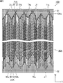
- the film capacitor 1 has a laminated body 10A, a first external electrode 51, and a second external electrode 52.
- the laminated body 10A has a first end surface 10Aa and a second end surface 10Ab facing each other in the width direction W.
- the laminated body 10A is a wound body in which the first metallized film 21A and the second metallized film 22A are wound in a state of being laminated in the thickness direction T. That is, the film capacitor 1 is a winding type film capacitor having a laminated body 10A which is also such a winding body.
- the cross-sectional shape of the laminated body 10A is flat when viewed in a cross section perpendicular to the winding axis direction (width direction W in FIG. 1) of the laminated body 10A from the viewpoint of reducing the height. Is preferable. More specifically, it is preferable that the cross-sectional shape of the laminated body 10A is pressed into a flat shape such as an ellipse or an oval, and the thickness is smaller than when the cross-sectional shape of the laminated body 10A is a perfect circle. ..
- Whether or not the laminated body is pressed so that the cross-sectional shape becomes flat can be confirmed by, for example, whether or not there are press marks on the laminated body.
- the film capacitor 1 may have a cylindrical winding shaft.
- the winding shaft is arranged on the central axis of the first metallized film 21A and the second metallized film 22A in the wound state, and winds the first metallized film 21A and the second metallized film 22A. It is the winding axis when doing so.
- the central axes of the first metallized film 21A and the second metallized film 22A in the wound state are not shown in FIG. 2, they are located on the left side.
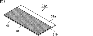
- the first metallized film 21A has a first dielectric film 31 and a first metal layer 41.
- the first dielectric film 31 has a first main surface 31a and a second main surface 31b facing the thickness direction T.
- the first metal layer 41 is provided on the first main surface 31a of the first dielectric film 31. More specifically, the first metal layer 41 reaches one side edge of the first dielectric film 31 in the width direction W on the first main surface 31a of the first dielectric film 31 and reaches the first dielectric. It is provided so as not to reach the other side edge of the body film 31.
- the second metallized film 22A has a second dielectric film 32 and a second metal layer 42.
- the second dielectric film 32 has a third main surface 32a and a fourth main surface 32b facing the thickness direction T.
- the second metal layer 42 is provided on the third main surface 32a of the second dielectric film 32. More specifically, the second metal layer 42 does not reach one side edge of the second dielectric film 32 in the width direction W on the third main surface 32a of the second dielectric film 32, and the second metal layer 42 does not reach the second side edge. It is provided so as to reach the other side edge of the dielectric film 32.
- the end portion of the first metal layer 41 on the side reaching the side edge of the first dielectric film 31 is exposed to the first end surface 10Aa of the laminated body 10A, and the second dielectric in the second metal layer 42.
- the width of the first metallized film 21A and the second metallized film 22A adjacent to each other in the thickness direction T is such that the end portion on the side reaching the side edge of the body film 32 is exposed to the second end surface 10Ab of the laminated body 10A. It is deviated in the direction W.
- the first metallized film 21A protrudes toward the first external electrode 51 with respect to the second metallized film 22A. ..
- the second metallized film 22A protrudes toward the second external electrode 52 with respect to the first metallized film 21A. ..
- the first metal layer 41 is connected to the first external electrode 51 and is not connected to the second external electrode 52.
- the second metal layer 42 is connected to the second external electrode 52 and is not connected to the first external electrode 51.
- the first dielectric film adjacent to the thickness direction T is formed.
- the first metal layer 41 is not provided on the main surface. 2 It projects toward the first external electrode 51 with respect to the dielectric film 32.
- the second dielectric film 32 in which the second metal layer 42 is provided on the third main surface 32a is the second. The metal layer 42 projects toward the second external electrode 52 with respect to the first dielectric film 31 which is not provided on the main surface.
- the laminated body 10A is wound in a state where the first metallized film 21A and the second metallized film 22A are laminated in the thickness direction T, the first dielectric film 31, the first metal layer 41, It can be said that the second dielectric film 32 and the second metal layer 42 are included in order in the thickness direction T. Further, the laminated body 10A is wound in a state where the first dielectric film 31, the first metal layer 41, the second dielectric film 32, and the second metal layer 42 are laminated in order in the thickness direction T. It can be said that it is a winding body.
- the first main surface 31a of the first dielectric film 31 and the fourth main surface 32b of the second dielectric film 32 face each other in the thickness direction T
- the second dielectric film 31 is the second.
- the main surface 31b and the third main surface 32a of the second dielectric film 32 face each other in the thickness direction T.
- the first metallized film 21A and the second metallized film 22A are wound in a state of being laminated in the thickness direction T.
- the first metallized film 21A is inside the second metallized film 22A, and more specifically, the first metal layer 41 is inside the first dielectric film 31.
- the first metallized film 21A and the second metallized film 22A are wound in a state of being laminated in the thickness direction T so that the two metal layer 42 is inside the second dielectric film 32. That is, in the laminated body 10A, the first metal layer 41 and the second metal layer 42 face each other with the first dielectric film 31 or the second dielectric film 32 interposed therebetween.
- the first metal layer 41 may be provided with a fuse portion.
- the fuse portion provided in the first metal layer 41 is a divided electrode portion in which the portion facing the second metal layer 42 is divided into a plurality of portions in the first metal layer 41, and a portion not facing the second metal layer 42. This is the part that connects to the electrode part.
- Examples of the electrode pattern of the first metal layer 41 provided with the fuse portion include the electrode patterns disclosed in JP-A-2004-363431 and JP-A-5-251266.
- the second metal layer 42 may also be provided with a fuse portion in the same manner as the first metal layer 41.
- the first dielectric film 31 may contain a curable resin as a main component.
- the main component means a component having the highest weight percentage, and preferably means a component having a weight percentage higher than 50% by weight.
- the curable resin may be a thermosetting resin or a photocurable resin.
- the thermosetting resin means a resin that can be cured by heat, but the curing method is not limited. Therefore, the thermosetting resin also includes a resin that can be cured by a method other than heat (for example, light, electron beam, etc.) as long as it is a resin that can be cured by heat. Further, depending on the material, the reaction may be started due to the reactivity of the material itself, and the resin that cures without necessarily applying heat or the like from the outside is also a thermosetting resin. The same applies to the photocurable resin, and as long as it is a resin that can be cured by light, a resin that can be cured by a method other than light (for example, heat) is also included.
- a method other than light for example, heat
- the curable resin is preferably composed of a cured product of a first organic material having a hydroxyl group (OH group) and a second organic material having an isocyanate group (NCO group).
- the curable resin is composed of a cured product having a urethane bond obtained by reacting the hydroxyl group of the first organic material with the isocyanate group of the second organic material.
- FT-IR Fourier transform infrared spectrophotometer
- the uncured portion of the starting material may remain in the first dielectric film 31.
- the first dielectric film 31 may contain at least one of a hydroxyl group and an isocyanate group.
- the first dielectric film 31 may contain either a hydroxyl group or an isocyanate group, or may contain both a hydroxyl group and an isocyanate group.
- the presence of hydroxyl groups and / or isocyanate groups in the first dielectric film 31 can be confirmed by analysis by FT-IR.
- Examples of the first organic material include phenoxy resin, polyvinyl acetal acetal resin, polyvinyl butyral resin and the like.
- the first organic material a plurality of types of organic materials may be used in combination.
- the second organic material examples include aromatic polyisocyanates such as diphenylmethane diisocyanate (MDI) and tolylene diisocyanate (TDI), and aliphatic polyisocyanates such as hexamethylene diisocyanate (HDI).
- aromatic polyisocyanates such as diphenylmethane diisocyanate (MDI) and tolylene diisocyanate (TDI)
- aliphatic polyisocyanates such as hexamethylene diisocyanate (HDI).
- HDI hexamethylene diisocyanate
- the second organic material a plurality of types of organic materials may be used in combination.
- the first dielectric film 31 may contain a thermoplastic resin as a main component.
- thermoplastic resin examples include polypropylene, polyether sulfone, polyetherimide, polyarylate and the like.
- the first dielectric film 31 may contain additives for adding various functions.
- Examples of the additive include a leveling agent for imparting smoothness.
- the additive has a functional group that reacts with a hydroxyl group and / or an isocyanate group and forms a part of the crosslinked structure of the cured product.
- an additive include a resin having at least one functional group selected from the group consisting of a hydroxyl group, an epoxy group, a silanol group, and a carboxyl group.
- the second dielectric film 32 may contain a curable resin as a main component, or may contain a thermoplastic resin as a main component. Further, the second dielectric film 32 may also contain an additive in the same manner as the first dielectric film 31.
- compositions of the first dielectric film 31 and the second dielectric film 32 may be different from each other, but are preferably the same.
- the thickness of the first dielectric film 31 and the second dielectric film 32 is preferably 1 ⁇ m or more and 10 ⁇ m or less, and more preferably 3 ⁇ m or more and 5 ⁇ m or less.
- the thicknesses of the first dielectric film 31 and the second dielectric film 32 may be different from each other, but are preferably the same.
- the thickness of the first dielectric film 31 and the second dielectric film 32 can be measured using an optical film thickness meter.
- the first dielectric film 31 and the second dielectric film 32 are each preferably produced by forming a resin solution containing the above-mentioned resin material into a film and then curing it by heat treatment.
- Examples of the constituent materials of the first metal layer 41 and the second metal layer 42 include metals such as aluminum, zinc, titanium, magnesium, tin, and nickel.
- compositions of the first metal layer 41 and the second metal layer 42 may be different from each other, but are preferably the same.
- the thickness of the first metal layer 41 and the second metal layer 42 is preferably 5 nm or more and 40 nm or less.
- the thicknesses of the first metal layer 41 and the second metal layer 42 may be different from each other, but are preferably the same.
- the thickness of the first metal layer 41 can be measured by observing the cut surface of the first metallized film 21A in the thickness direction using a transmission electron microscope (TEM).
- the thickness of the second metal layer 42 can be measured in the same manner as the thickness of the first metal layer 41.
- the first metal layer 41 and the second metal layer 42 are preferably formed by depositing the above-mentioned metal on the main surfaces of the first dielectric film 31 and the second dielectric film 32, respectively.
- the first external electrode 51 is connected to the first end surface 10Aa of the laminated body 10A. More specifically, the first external electrode 51 is connected to the first metal layer 41 by coming into contact with the end portion of the first metal layer 41 exposed on the first end surface 10Aa of the laminated body 10A. On the other hand, the first external electrode 51 is not connected to the second metal layer 42.
- the second external electrode 52 is connected to the second end surface 10Ab of the laminated body 10A. More specifically, the second external electrode 52 is connected to the second metal layer 42 by coming into contact with the end portion of the second metal layer 42 exposed on the second end surface 10Ab of the laminated body 10A. On the other hand, the second external electrode 52 is not connected to the first metal layer 41.
- Examples of the constituent materials of the first external electrode 51 and the second external electrode 52 include metals such as zinc, aluminum, tin, and zinc-aluminum alloy.
- composition of the first external electrode 51 and the second external electrode 52 may be different from each other, but it is preferable that they are the same as each other.
- the first external electrode 51 and the second external electrode 52 are preferably formed by spraying the metal as described above onto the first end surface 10Aa and the second end surface 10Ab of the laminated body 10A, respectively.
- the first metal layer 41 is provided on the first main surface 31a on the first end surface 10Aa of the laminated body 10A.
- the first unevenness 11a having a curve J1 connecting the ends of the first dielectric film 31 as a contour line continuously exists in the thickness direction T. More specifically, the curve J1 is a curve connecting the center points of the end portions of the first dielectric film 31 in the thickness direction T.
- the first end surface 10Aa is defined by the curve J1 and the shape thereof is the uneven shape defined by the first unevenness 11a.
- the first external electrode 51 is connected to the first end surface 10Aa of the laminated body 10A, but more specifically, the first external electrode 51 fills the concave portion of the first unevenness 11a. It is connected to the first end surface 10Aa of the laminated body 10A. As described above, the presence of the first unevenness 11a on the first end surface 10Aa of the laminated body 10A makes it easy to increase the contact area between the first metallized film 21A and the first external electrode 51.
- the film capacitor 1 is used so as to repeat a low temperature state and a high temperature state, in order to realize a state in which the increase in equivalent series resistance is suppressed, the first end surface 10Aa of the laminated body 10A is first.
- the presence of the unevenness 11a is not sufficient, and it is important that the specifications of the film capacitor 1 are as follows.
- the first unevenness 11a has a height of 0.07 mm or more and 0.25 mm or less, and an interval of 0.07 mm or more and 0.15 mm or less. be.
- the contact area between the first metallized film 21A and the first external electrode 51 becomes sufficiently large, so that the bondability between the first metallized film 21A and the first external electrode 51 tends to be improved. Therefore, when the film capacitor 1 is used so as to repeat a low temperature state and a high temperature state, the resistance to the tensile stress generated in the first external electrode 51 is increased, and the tensile stress causes the first metallized film 21A to be the first external. It is difficult to peel off from the electrode 51, and the bonded state of the first metallized film 21A and the first external electrode 51 is easily maintained.
- the contact area between the first metallized film 21A and the first external electrode 51 becomes insufficient, so that the first metallized film 21A and the first external electrode It becomes difficult to improve the bondability with 51.
- the first dielectric film 31 collapses and the concave portion of the first unevenness 11a is easily closed. Therefore, the first external electrode 51 is formed by spraying metal. At that time, it becomes difficult for the sprayed metal to enter the concave portion of the first unevenness 11a. As a result, the contact area between the first metallized film 21A and the first external electrode 51 becomes insufficient, so that the bondability between the first metallized film 21A and the first external electrode 51 is less likely to increase.
- the distance between the first unevenness 11a is smaller than 0.07 mm
- the first external electrode 51 is formed by spraying metal, it becomes difficult for the sprayed metal to enter the concave portion of the first unevenness 11a.
- the contact area between the first metallized film 21A and the first external electrode 51 becomes insufficient, so that the bondability between the first metallized film 21A and the first external electrode 51 is less likely to increase.
- the contact area between the first metallized film 21A and the first external electrode 51 becomes insufficient, so that the first metallized film 21A and the first external electrode 51 It becomes difficult to improve the bondability with.
- a first gap 71a exists between the second dielectric film 32 on which the first metal layer 41 is not provided on the main surface and the first external electrode 51.
- the second dielectric film 32 and the first external electrode 51 are provided apart from each other in the width direction W by the amount of the presence of the first gap 71a.
- both ends of the first gap 71a in the width direction W are defined by the second dielectric film 32 and the first external electrode 51.
- both ends of the first gap 71a in the thickness direction T are defined by a part of the first metallized film 21A facing the second dielectric film 32.
- the length of the first gap 71a in the width direction W is 0.3 mm or more.
- the compressive stress generated in the first external electrode 51 is less likely to be buffered.
- the length of the first gap 71a in the width direction W is preferably 1.5 mm or less.
- the length of the first gap 71a in the width direction W is preferably 0.5 mm or more and 1.5 mm or less.
- the first dielectric film 31 is located on the first external electrode 51 side with respect to the second dielectric film 32.
- the length of the first gap 71a in the width direction W may be equal to or less than the protrusion length in the width direction W of the first dielectric film 31 with respect to the second dielectric film 32. More specifically, the length of the first gap 71a in the width direction W may be the same as the protrusion length of the first dielectric film 31 with respect to the second dielectric film 32 in the width direction W, or the second. It may be smaller than the protrusion length in the width direction W of the first dielectric film 31 with respect to the dielectric film 32.
- the height and spacing of the first unevenness 11a are in the above-mentioned range, and the length of the first gap 71a in the width direction W is in the above-mentioned range.
- the resistance to tensile stress is increased and the compressive stress is easily buffered. Therefore, the boundary between the first metallized film 21A and the first external electrode 51. The occurrence of cracks in the vicinity is suppressed. Therefore, in the film capacitor 1, even if the film capacitor 1 is used so as to repeat a low temperature state and a high temperature state, an increase in equivalent series resistance can be suppressed.
- the second metal layer 42 is provided on the third main surface 32a on the second end surface 10Ab of the laminated body 10A.
- the second unevenness 12a whose contour line is the curve J2 connecting the ends of the second dielectric film 32 is continuously present in the thickness direction T. More specifically, the curve J2 is a curve connecting the center points of the end portions of the second dielectric film 32 in the thickness direction T. It can be said that in the laminated body 10A, the second end surface 10Ab is defined by the curve J2, and the shape thereof is the concave-convex shape defined by the second unevenness 12a.
- the second external electrode 52 is connected to the second end surface 10Ab of the laminated body 10A, but more specifically, the second external electrode 52 fills the concave portion of the second unevenness 12a. It is connected to the second end surface 10Ab of the laminated body 10A. As described above, the presence of the second unevenness 12a on the second end surface 10Ab of the laminated body 10A makes it easy to increase the contact area between the second metallized film 22A and the second external electrode 52.
- the second unevenness 12a when measured in accordance with JIS B 0601: 2001, the second unevenness 12a has a height of 0.07 mm or more and 0.25 mm or less, and an interval of 0.07 mm or more and 0.15 mm or less. be.
- the contact area between the second metallized film 22A and the second external electrode 52 becomes sufficiently large, so that the bondability between the second metallized film 22A and the second external electrode 52 tends to be improved. Therefore, when the film capacitor 1 is used so as to repeat a low temperature state and a high temperature state, the resistance to the tensile stress generated in the second external electrode 52 is increased, and the tensile stress causes the second metallized film 22A to be second outside. It is difficult to peel off from the electrode 52, and the bonded state between the second metallized film 22A and the second external electrode 52 is easily maintained.
- the height of the second unevenness 12a may be the same as or different from the height of the first unevenness 11a.
- the distance between the second unevenness 12a may be the same as or different from the distance between the first unevenness 11a.
- a second gap 72a exists between the first dielectric film 31 on which the second metal layer 42 is not provided on the main surface and the second external electrode 52.
- the first dielectric film 31 and the second external electrode 52 are provided apart from each other in the width direction W by the extent that the second gap 72a exists.
- both ends of the second gap 72a in the width direction W are defined by the first dielectric film 31 and the second external electrode 52.
- both ends of the second gap 72a in the thickness direction T are defined by a part of the second metallized film 22A facing each other with the first dielectric film 31 interposed therebetween.
- the length of the second gap 72a in the width direction W is 0.3 mm or more.
- the length of the second gap 72a in the width direction W is preferably 1.5 mm or less.
- the length of the second gap 72a in the width direction W is preferably 0.5 mm or more and 1.5 mm or less.
- the length of the second gap 72a in the width direction W may be the same as or different from the length of the first gap 71a in the width direction W.
- the second dielectric film 32 is located on the second external electrode 52 side with respect to the first dielectric film 31.
- the length of the second gap 72a in the width direction W may be equal to or less than the protrusion length in the width direction W of the second dielectric film 32 with respect to the first dielectric film 31. More specifically, the length of the second gap 72a in the width direction W may be the same as the protrusion length of the second dielectric film 32 with respect to the first dielectric film 31 in the width direction W, or the first. It may be smaller than the protrusion length in the width direction W of the second dielectric film 32 with respect to the dielectric film 31.
- the height and spacing of the second unevenness 12a are in the above-mentioned range, and the length of the second gap 72a in the width direction W is in the above-mentioned range.
- the resistance to tensile stress is increased and the compressive stress is easily buffered. Therefore, the boundary between the second metallized film 22A and the second external electrode 52. The occurrence of cracks in the vicinity is suppressed. Therefore, in the film capacitor 1, even if the film capacitor 1 is used so as to repeat a low temperature state and a high temperature state, an increase in equivalent series resistance can be suppressed.
- the sample prepared as follows is used.
- FIG. 3 is a schematic perspective view showing a sample for defining the specifications of the film capacitor.
- a sample having a cross section as shown in FIG. 3 is obtained by sealing the periphery of the film capacitor 1 shown in FIG. 1 with a sealing resin and then cutting the film using a precision cutting machine “ISOMET1000” manufactured by Buehler. Cut out 100.
- the sealing resin used for sealing the periphery of the film capacitor 1 is omitted.
- the rotation speed of the sample holder and the rotation speed of the polishing plate are set to 150 rpm, respectively.
- the order of use of the SiC water-resistant polishing paper is 320 for 10 minutes and 600 for 3 minutes. , 1000 for 3 minutes, 1500 for 3 minutes.
- a diamond suspension having an abrasive grain size of 3 ⁇ m and 1 ⁇ m is used to perform a mirror finish on the cross section of the sample 100.
- the sample 100 for defining the specifications of the film capacitor 1 is prepared.
- the height of the first unevenness 11a is determined as follows in the sample 100 shown in FIG.
- FIG. 4 is a part of the cross section of the sample in FIG. 3, and is a schematic cross-sectional view for explaining a method of determining the height of the first unevenness.
- the cross section of the sample 100 shown in FIG. 3 is magnified 75 times or more and 200 times or less, and the cross section of the sample 100 as shown in FIG. 4 is observed. ..
- an image analysis software is used to draw a curve J1 connecting the ends of the first dielectric film 31 on the side of the first external electrode 51. More specifically, the curve J1 is a curve connecting the center points of the end portion of the first dielectric film 31 in the thickness direction T.
- the height H1 and the height of five contour curve elements (a set of adjacent peaks and valleys) continuous in the thickness direction T in accordance with JIS B 0601: 2001.
- the height H2, the height H3, the height H4, and the height H5 are measured.
- the metallized film is divided into three equal parts in the thickness direction T in order from the winding start position P1 to the winding end position P2. This is performed at each center of the region R1, the region R2, and the region R3 in the thickness direction T.
- a total of 15 measured values of the heights of the contour curve elements can be obtained in the regions R1, the region R2, and the region R3.
- the average value of these 15 measured values is calculated, and this average value is defined as the height of the first unevenness 11a.
- the height of the contour curve element is measured with respect to the curve J1 connecting the ends of the first dielectric film 31 on the side of the first external electrode 51. Is going.
- the curve J1'connecting the ends of the first dielectric film 31 on the side of the second external electrode 52 also has the same uneven shape as the first unevenness 11a.
- the first external electrode 51 is formed by spraying metal
- the end portion of the first dielectric film 31 on the second external electrode 52 side is compared with the end portion on the first external electrode 51 side. Therefore, since it is not easily affected by thermal spraying of metal, the curve J1'may be easier to determine clearly than the curve J1.
- the height of the contour curve element may be measured with respect to the curve J1'.
- the measurement of H4'and the height H5' may be performed in the same manner as described above, except that the measurement is performed at each center of the region R1, the region R2, and the region R3 in the thickness direction T.
- the average value of the heights of the contour curve elements obtained with respect to the curve J1 and the average value of the heights of the contour curve elements obtained with respect to the curve J1' are significant. If there is a significant difference at the level 5%, priority is given to the average value of the heights of the contour curve elements obtained with respect to the curve J1'.
- the height of the second unevenness 12a is also determined in the same manner as the height of the first unevenness 11a.
- the interval between the first unevenness 11a is determined as follows in the sample 100 shown in FIG.
- FIG. 5 is a part of the cross section of the sample in FIG. 3, and is a schematic cross-sectional view for explaining a method of determining the interval of the first unevenness.
- D1, length D2, length D3, length D4, and length D5 are measured.
- the measurement of the length of such a contour curve element is performed at each center of the region R1, the region R2, and the region R3 in the thickness direction T in the cross section of the sample 100 shown in FIG.
- a total of 15 measured values of the lengths of the contour curve elements can be obtained in the regions R1, the regions R2, and the regions R3.
- the average value of these 15 measured values is calculated, and this average value is defined as the interval of the first unevenness 11a.
- the length of the contour curve element may be measured with respect to the curve J1'in the same manner as when determining the height of the first unevenness 11a.
- the length D1', the length D2', the length D3', and the length of the five contour curve elements continuous in the thickness direction T in accordance with JIS B 0601: 2001.
- the measurement of D4'and the length D5' may be performed in the same manner as described above, except that the measurement is performed at each center of the region R1, the region R2, and the region R3 in the thickness direction T.
- the average value of the lengths of the contour curve elements obtained with respect to the curve J1 and the average value of the lengths of the contour curve elements obtained with respect to the curve J1' are significant levels. If there is a significant difference at 5%, priority is given to the average value of the lengths of the contour curve elements obtained for the curve J1'.
- the spacing between the second unevenness 12a is also determined in the same manner as the spacing between the first unevenness 11a.
- the length of the first gap 71a in the width direction W is determined as follows in the sample 100 shown in FIG.
- FIG. 6 is a partial cross-sectional view of the sample in FIG. 3 and is a schematic cross-sectional view for explaining a method of determining the length of the first gap in the width direction.
- a curve K connecting the ends in contact with the first gap 71a in the first external electrode 51 is drawn by using image analysis software. More specifically, the curve K is a curve connecting the center points of the end portion of the first external electrode 51 in the thickness direction T. Further, using image analysis software, a curve J2'connecting the ends of the second dielectric film 32 on the side of the first external electrode 51 is drawn. More specifically, the curve J2'is a curve connecting the center points of the end portion of the second dielectric film 32 in the thickness direction T. Next, using image analysis software, a center line M1 for the curve K and a center line M2 for the curve J2'are drawn according to JIS B 0601: 2001.
- the distance L1 between the center lines which is the distance in the width direction W between the center line M1 and the center line M2, is measured.
- Such measurement of the distance between the center lines is performed at each center of the region R1, the region R2, and the region R3 in the thickness direction T in the cross section of the sample 100 shown in FIG.
- a total of three measured values of the distance between the center lines can be obtained in the regions R1, the region R2, and the region R3.
- the average value of these three measured values is calculated, and this average value is defined as the length of the first gap 71a in the width direction W.
- the length of the second gap 72a in the width direction W is also determined in the same manner as the length of the first gap 71a in the width direction W.
- the film capacitor 1 is manufactured by, for example, the following method.
- FIG. 7 is a schematic perspective view showing a process of manufacturing a first metallized film for an example of the method for manufacturing a film capacitor according to the first embodiment of the present invention.
- FIG. 8 is a schematic perspective view showing a process of manufacturing a second metallized film for an example of the method for manufacturing a film capacitor according to the first embodiment of the present invention.
- a resin solution is prepared by mixing the above-mentioned first organic material, second organic material, additives and the like. Then, the obtained resin solution is formed into a film and then cured by heat treatment to produce a first dielectric film 31 and a second dielectric film 32 as shown in FIGS. 7 and 8.
- a metal such as aluminum, zinc, titanium, magnesium, tin, or nickel is vapor-deposited on the first main surface 31a of the first dielectric film 31 to form the first metal layer 41.
- the first metallized film 21A is produced.
- the first metal layer 41 is formed so as to reach one side edge of the first dielectric film 31 and not reach the other side edge of the first dielectric film 31 in the width direction.
- a metal such as aluminum, zinc, titanium, magnesium, tin, or nickel is vapor-deposited on the third main surface 32a of the second dielectric film 32 to form the second metal layer 42.
- the second metallized film 22A is produced.
- the second metal layer 42 is formed so as not to reach one side edge of the second dielectric film 32 in the width direction but to reach the other side edge of the second dielectric film 32.
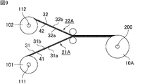
- FIG. 9 is a schematic cross-sectional view showing a manufacturing process of a laminated body for an example of the method for manufacturing a film capacitor according to the first embodiment of the present invention.
- the second film reel 102 is prepared.
- the first metallized film 21A is unwound from the first film reel 101, and the second metallized film 22A is unwound from the second film reel 102.
- the first metallized film 21A and the second metallized film 22A are wound so that the second main surface 31b of the first dielectric film 31 and the third main surface 32a of the second dielectric film 32 face each other. put out.
- the unwound first metallized film 21A and the second metallized film 22A are wound around the winding shaft 200 in a state of being displaced and overlapped in the width direction.
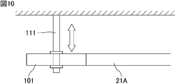
- FIG. 10 is a schematic view showing a state in which the first metallized film is unwound from the first film reel in FIG. 9 as viewed from above.
- the first reel shaft 111 periodically swings in the width direction (direction indicated by the double-headed arrow), so that the first metallized film 21A is unwound while periodically moving in the same width direction. Is done.
- the second reel shaft 112 is periodically swung in the width direction orthogonal to the unwinding direction.
- the second metallized film 22A is unwound while periodically moving in the same width direction.
- the first metallized film 21A and the second metallized film 22A are unwound while periodically moving in the width direction, so that the first unevenness 11a as shown in FIG. 2 is formed on the first end surface 10Aa.
- the laminated body 10A that exists and has the second unevenness 12a on the second end surface 10Ab is produced in a state of being wound around the winding shaft 200.
- the height and spacing of the first unevenness 11a are adjusted by adjusting swing conditions such as swing timing, swing cycle, and swing distance.
- the height and spacing of the second unevenness 12a can be adjusted.
- the height and spacing of the first unevenness 11a and the second unevenness 12a can also be adjusted.
- the height and spacing of the reels can be adjusted.
- the first unevenness The distance between the 11a and the second unevenness 12a are about the same.
- the first reel The larger the swing distance of the shaft 111 and the second reel shaft 112, the larger the height of the first unevenness 11a and the height of the second unevenness 12a.
- the winding shaft 200 is swung in the width direction, and the first metallized film 21A and the second metallized film 22A are used. Even if the traveling roller to be traveled is swung in the width direction, the laminated body 10A as shown in FIG. 2 can be manufactured in a state of being wound around the winding shaft 200.
- the obtained laminated body 10A may be sandwiched from a direction orthogonal to the width direction and pressed into an elliptical cylindrical shape.
- the first external electrode 51 shown in FIG. 2 is connected to the first metal layer 41 by spraying a metal such as zinc, aluminum, tin, or a zinc-aluminum alloy onto the first end surface 10Aa of the laminate 10A. Form to be.
- a metal such as zinc, aluminum, tin, or a zinc-aluminum alloy
- the first gap 71a shown in FIG. 2 is combined with the second dielectric film 32.
- the length of the first gap 71a in the width direction can be adjusted while being provided between the first external electrode 51 and the first external electrode 51.
- the second external electrode 52 shown in FIG. 2 is attached to the second metal layer 42. Formed to be connected to.
- the thermal spraying conditions such as the distance from the thermal spray nozzle to the second end surface 10Ab of the laminated body 10A and the air pressure of the thermal spray nozzle, the second gap 72a shown in FIG. 2 is combined with the first dielectric film 31.
- the length of the second gap 72a in the width direction can be adjusted while being provided between the second external electrode 52 and the second external electrode 52.
- the periphery of the laminated body 10A, the first external electrode 51, and the second external electrode 52 May be sealed with a resin.
- the film capacitor 1 shown in FIGS. 1 and 2 is manufactured.
- the second metal layer is provided on the second main surface of the first dielectric film.
- FIG. 11 is a schematic cross-sectional view showing an example of the film capacitor of the second embodiment of the present invention.
- the film capacitor 2 has a laminated body 10B, a first external electrode 51, and a second external electrode 52.
- the laminated body 10B has a first end surface 10Ba and a second end surface 10Bb facing each other in the width direction W.
- the laminated body 10B is a wound body in which the first metallized film 21B and the second dielectric film 32 are wound in a state of being laminated in the thickness direction T.
- the first metallized film 21B has a first dielectric film 31, a first metal layer 41, and a second metal layer 42.
- the first metal layer 41 is provided on the first main surface 31a of the first dielectric film 31 in the same manner as the laminated body 10A shown in FIG. More specifically, the first metal layer 41 reaches one side edge of the first dielectric film 31 in the width direction W on the first main surface 31a of the first dielectric film 31 and reaches the first dielectric. It is provided so as not to reach the other side edge of the body film 31.
- the second metal layer 42 is provided on the second main surface 31b of the first dielectric film 31, unlike the laminated body 10A shown in FIG. More specifically, the second metal layer 42 does not reach one side edge of the first dielectric film 31 in the width direction W on the second main surface 31b of the first dielectric film 31, and is the first. It is provided so as to reach the other side edge of the dielectric film 31.
- the first dielectric film 31 is longer in the width direction W than the second dielectric film 32, so that the first dielectric film 31 reaches the side edge of the first dielectric film 31 in the first metal layer 41.
- the side end is exposed on the first end surface 10Ba of the laminate 10B, and the end on the side reaching the side edge of the first dielectric film 31 in the second metal layer 42 is on the second end surface 10Bb of the laminate 10B. It is exposed. That is, in the first metallized film 21B and the second dielectric film 32 adjacent to each other in the thickness direction T, the first metallized film 21B is on the side of the first external electrode 51 and the second outside with respect to the second dielectric film 32. It protrudes toward the electrode 52. In such a state, the first metal layer 41 is connected to the first external electrode 51 and is not connected to the second external electrode 52. Further, the second metal layer 42 is connected to the second external electrode 52 and is not connected to the first external electrode 51.
- the first dielectric film 31 and the second dielectric film 31 adjacent to each other in the thickness direction T are in a positional relationship as described above.
- the first dielectric film 31 in which the first metal layer 41 is provided on the first main surface 31a is a second dielectric in which the first metal layer 41 is not provided on the main surface. It protrudes toward the first external electrode 51 with respect to the film 32.
- the first dielectric film 31 in which the second metal layer 42 is provided on the second main surface 31b is the second.
- the metal layer 42 projects toward the second external electrode 52 with respect to the second dielectric film 32 which is not provided on the main surface.
- the first end surface 10Ba of the laminated body 10B has the same as the first end surface 10Aa of the laminated body 10A shown in FIG.
- the first unevenness 11a whose contour line is the curve J1 connecting the ends of the first dielectric film 31 in which the first metal layer 41 is provided on the first main surface 31a is continuously present in the thickness direction T. are doing.
- the height of the first unevenness 11a is 0.07 mm or more and 0.25 mm or less when measured in accordance with JIS B 0601: 2001, similarly to the film capacitor 1 shown in FIG.
- the interval is 0.07 mm or more and 0.15 mm or less.
- the second dielectric film 32 and the first external electrode 51 on which the first metal layer 41 is not provided on the main surface are provided. There is a first gap 71a between them.
- the length of the first gap 71a in the width direction W is 0.3 mm or more, similar to the film capacitor 1 shown in FIG.
- the second metal layer 42 is provided on the second main surface 31b on the second end surface 10Bb of the laminated body 10B.
- the second unevenness 12b whose contour line is the curve J3 connecting the ends of the first dielectric film 31 is continuously present in the thickness direction T. More specifically, the curve J3 is a curve connecting the center points of the end portions of the first dielectric film 31 in the thickness direction T. It can be said that in the laminated body 10B, the second end surface 10Bb is defined by the curve J3, and the shape thereof is the concave-convex shape defined by the second unevenness 12b.
- the second unevenness 12b when measured in accordance with JIS B 0601: 2001, has a height of 0.07 mm or more and 0.25 mm or less, and an interval of 0.07 mm or more and 0.15 mm or less. be.
- the height of the second unevenness 12b is determined in the same manner as the height of the first unevenness 11a.
- the distance between the second unevenness 12b is determined in the same manner as the distance between the first unevenness 11a.
- a second gap 72b exists between the second dielectric film 32 on which the second metal layer 42 is not provided on the main surface and the second external electrode 52. There is.
- the length of the second gap 72b in the width direction W is 0.3 mm or more.
- the length of the second gap 72b in the width direction W is preferably 1.5 mm or less.
- the length of the second gap 72b in the width direction W is preferably 0.5 mm or more and 1.5 mm or less.
- the length of the second gap 72b in the width direction W may be the same as or different from the length of the first gap 71a in the width direction W.
- the length of the second gap 72b in the width direction W is determined in the same manner as the length of the first gap 71a in the width direction W.
- the first dielectric film 31 is located on the second external electrode 52 side with respect to the second dielectric film 32.
- the length of the second gap 72b in the width direction W may be equal to or less than the protrusion length in the width direction W of the first dielectric film 31 with respect to the second dielectric film 32. More specifically, the length of the second gap 72b in the width direction W may be the same as the protrusion length of the first dielectric film 31 with respect to the second dielectric film 32 in the width direction W, or the second. It may be smaller than the protrusion length in the width direction W of the first dielectric film 31 with respect to the dielectric film 32.
- the height and spacing of the first unevenness 11a and the second unevenness 12b are within the above-mentioned ranges, and the lengths of the first gap 71a and the second gap 72b in the width direction W are set. Within the above range, the same effect as that of the film capacitor 1 shown in FIG. 2 can be obtained.
- the second metal layer is separated from the first metal layer on the first main surface of the first dielectric film.
- a third metal layer that is provided and is not connected to the first external electrode and the second external electrode is provided on the third main surface of the second dielectric film.
- FIG. 12 is a schematic cross-sectional view showing an example of the film capacitor of the third embodiment of the present invention.
- the film capacitor 3 has a laminated body 10C, a first external electrode 51, and a second external electrode 52.
- the laminated body 10C has a first end surface 10Ca and a second end surface 10Cb facing each other in the width direction W.
- the laminated body 10C is a wound body in which the first metallized film 21C and the second metallized film 22B are wound in a state of being laminated in the thickness direction T.
- the first metallized film 21C has a first dielectric film 31, a first metal layer 41, and a second metal layer 42.
- the first metal layer 41 is provided on the first main surface 31a of the first dielectric film 31 in the same manner as the laminated body 10A shown in FIG. More specifically, the first metal layer 41 reaches one side edge of the first dielectric film 31 in the width direction W on the first main surface 31a of the first dielectric film 31 and reaches the first dielectric. It is provided so as not to reach the other side edge of the body film 31.
- the second metal layer 42 is provided on the first main surface 31a of the first dielectric film 31 at a distance from the first metal layer 41. There is. More specifically, the second metal layer 42 does not reach one side edge of the first dielectric film 31 in the width direction W on the first main surface 31a of the first dielectric film 31, and is the first. It is provided so as to reach the other side edge of the dielectric film 31.
- the second metallized film 22B has a second dielectric film 32 and a third metal layer 43.
- a third metal layer 43 is provided on the third main surface 32a of the second dielectric film 32. More specifically, the third metal layer 43 is formed on one side edge and the other side edge of the second dielectric film 32 in the width direction W on the third main surface 32a of the second dielectric film 32. It is provided so that it will not reach.
- the first dielectric film 31 is longer in the width direction W than the second dielectric film 32, so that the first dielectric film 31 reaches the side edge of the first dielectric film 31 in the first metal layer 41.
- the side end is exposed on the first end surface 10Ca of the laminate 10C, and the end on the side reaching the side edge of the first dielectric film 31 in the second metal layer 42 is on the second end surface 10Cb of the laminate 10C. It is exposed. That is, in the first metallized film 21C and the second metallized film 22B adjacent to each other in the thickness direction T, the first metallized film 21C is on the side of the first external electrode 51 and the second outside with respect to the second metallized film 22B. It protrudes toward the electrode 52.
- the first metal layer 41 is connected to the first external electrode 51 and is not connected to the second external electrode 52.
- the second metal layer 42 is connected to the second external electrode 52 and is not connected to the first external electrode 51.
- the third metal layer 43 is not connected to the first external electrode 51 and the second external electrode 52.
- the capacitor composed of the first metal layer 41 and the third metal layer 43 and the capacitor composed of the second metal layer 42 and the third metal layer 43 are connected in series. It will be.
- the first dielectric film 31 and the first dielectric film 31 adjacent to each other in the thickness direction T are in a positional relationship as described above.
- the first dielectric film 31 in which the first metal layer 41 is provided on the first main surface 31a is a second dielectric in which the first metal layer 41 is not provided on the main surface. It protrudes toward the first external electrode 51 with respect to the film 32.
- the first dielectric film 31 in which the second metal layer 42 is provided on the first main surface 31a is the second.
- the metal layer 42 projects toward the second external electrode 52 with respect to the second dielectric film 32 which is not provided on the main surface.
- the first end surface 10Ca of the laminated body 10C has the same as the first end surface 10Aa of the laminated body 10A shown in FIG.
- the first unevenness 11a whose contour line is the curve J1 connecting the ends of the first dielectric film 31 in which the first metal layer 41 is provided on the first main surface 31a is continuously present in the thickness direction T. are doing.
- the height of the first unevenness 11a is 0.07 mm or more and 0.25 mm or less when measured in accordance with JIS B 0601: 2001.
- the interval is 0.07 mm or more and 0.15 mm or less.
- the second dielectric film 32 and the first external electrode 51 are provided with the first metal layer 41 not provided on the main surface. There is a first gap 71a between them.
- the length of the first gap 71a in the width direction W is 0.3 mm or more, similar to the film capacitor 1 shown in FIG.
- the second metal layer 42 is provided on the first main surface 31a on the second end surface 10Cb of the laminated body 10C.
- the second unevenness 12b whose contour line is the curve J3 connecting the ends of the first dielectric film 31 is continuously present in the thickness direction T. It can be said that in the laminated body 10C, the second end surface 10Cb is defined by the curve J3, and the shape thereof is the concave-convex shape defined by the second unevenness 12b.
- the second unevenness 12b when measured in accordance with JIS B 0601: 2001, has a height of 0.07 mm or more and 0.25 mm or less, and an interval of 0.07 mm or more and 0.15 mm or less. be.
- a second gap 72b exists between the second dielectric film 32 on which the second metal layer 42 is not provided on the main surface and the second external electrode 52. There is.
- the length of the second gap 72b in the width direction W is 0.3 mm or more.
- the height and spacing of the first unevenness 11a and the second unevenness 12b are within the above-mentioned ranges, and the lengths of the first gap 71a and the second gap 72b in the width direction W are set. Within the above range, the same effect as that of the film capacitor 1 shown in FIG. 2 can be obtained.
- the second metal layer is separated from the first metal layer on the first main surface of the first dielectric film.
- a third metal layer that is provided and is not connected to the first external electrode and the second external electrode is provided on the second main surface of the first dielectric film.
- FIG. 13 is a schematic cross-sectional view showing an example of the film capacitor of the fourth embodiment of the present invention.
- the film capacitor 4 has a laminated body 10D, a first external electrode 51, and a second external electrode 52.
- the laminated body 10D has a first end surface 10Da and a second end surface 10Db facing each other in the width direction W.
- the laminated body 10D is a wound body in which the first metallized film 21D and the second dielectric film 32 are wound in a state of being laminated in the thickness direction T.
- the first metallized film 21D has a first dielectric film 31, a first metal layer 41, a second metal layer 42, and a third metal layer 43.
- the first metal layer 41 is provided on the first main surface 31a of the first dielectric film 31 in the same manner as the laminated body 10A shown in FIG. More specifically, the first metal layer 41 reaches one side edge of the first dielectric film 31 in the width direction W on the first main surface 31a of the first dielectric film 31 and reaches the first dielectric. It is provided so as not to reach the other side edge of the body film 31.
- the second metal layer 42 is provided on the first main surface 31a of the first dielectric film 31 at a distance from the first metal layer 41. There is. More specifically, the second metal layer 42 does not reach one side edge of the first dielectric film 31 in the width direction W on the first main surface 31a of the first dielectric film 31, and is the first. It is provided so as to reach the other side edge of the dielectric film 31.
- a third metal layer 43 is provided on the second main surface 31b of the first dielectric film 31. More specifically, the third metal layer 43 is formed on one side edge and the other side edge of the first dielectric film 31 in the width direction W on the second main surface 31b of the first dielectric film 31. It is provided so that it will not reach.
- no metal layer is provided on both main surfaces of the third main surface 32a and the fourth main surface 32b of the second dielectric film 32.
- the first dielectric film 31 is longer in the width direction W than the second dielectric film 32, so that the first dielectric film 31 reaches the side edge of the first dielectric film 31 in the first metal layer 41.
- the side end is exposed on the first end surface 10Da of the laminate 10D, and the end on the side reaching the side edge of the first dielectric film 31 in the second metal layer 42 is on the second end surface 10Db of the laminate 10D. It is exposed. That is, in the first metallized film 21D and the second dielectric film 32 adjacent to each other in the thickness direction T, the first metallized film 21D is on the side of the first external electrode 51 and the second outside with respect to the second dielectric film 32. It protrudes toward the electrode 52.
- the first metal layer 41 is connected to the first external electrode 51 and is not connected to the second external electrode 52.
- the second metal layer 42 is connected to the second external electrode 52 and is not connected to the first external electrode 51.
- the third metal layer 43 is not connected to the first external electrode 51 and the second external electrode 52.
- the capacitor composed of the first metal layer 41 and the third metal layer 43 and the capacitor composed of the second metal layer 42 and the third metal layer 43 are connected in series. It will be.
- the first dielectric film 31 and the second dielectric film 31 adjacent to each other in the thickness direction T are in a positional relationship as described above.
- the first dielectric film 31 in which the first metal layer 41 is provided on the first main surface 31a is a second dielectric in which the first metal layer 41 is not provided on the main surface. It protrudes toward the first external electrode 51 with respect to the film 32.
- the first dielectric film 31 in which the second metal layer 42 is provided on the first main surface 31a is the second.
- the metal layer 42 projects toward the second external electrode 52 with respect to the second dielectric film 32 which is not provided on the main surface.
- the first end surface 10Da of the laminated body 10D has the same as the first end surface 10Aa of the laminated body 10A shown in FIG.
- the first unevenness 11a whose contour line is the curve J1 connecting the ends of the first dielectric film 31 in which the first metal layer 41 is provided on the first main surface 31a is continuously present in the thickness direction T. are doing.
- the height of the first unevenness 11a is 0.07 mm or more and 0.25 mm or less when measured in accordance with JIS B 0601: 2001.
- the interval is 0.07 mm or more and 0.15 mm or less.
- the second dielectric film 32 and the first external electrode 51 are provided with the first metal layer 41 not provided on the main surface. There is a first gap 71a between them.
- the length of the first gap 71a in the width direction W is 0.3 mm or more, similar to the film capacitor 1 shown in FIG.
- the second metal layer 42 is provided on the first main surface 31a on the second end surface 10Db of the laminated body 10D.
- the second unevenness 12b whose contour line is the curve J3 connecting the ends of the first dielectric film 31 is continuously present in the thickness direction T. It can be said that in the laminated body 10D, the second end surface 10Db is defined by the curve J3, and the shape thereof is the concave-convex shape defined by the second unevenness 12b.
- the second unevenness 12b when measured in accordance with JIS B 0601: 2001, has a height of 0.07 mm or more and 0.25 mm or less, and an interval of 0.07 mm or more and 0.15 mm or less. be.
- a second gap 72b exists between the second dielectric film 32 on which the second metal layer 42 is not provided on the main surface and the second external electrode 52. There is.
- the length of the second gap 72b in the width direction W is 0.3 mm or more.
- the height and spacing of the first unevenness 11a and the second unevenness 12b are within the above-mentioned ranges, and the lengths of the first gap 71a and the second gap 72b in the width direction W are set. Within the above range, the same effect as that of the film capacitor 1 shown in FIG. 2 can be obtained.
- Film capacitor samples 1 to 45 were manufactured by the following method.
- a resin solution was prepared by mixing a phenoxy resin, which is a bisphenol A type epoxy resin as a first organic material, and MDI as a second organic material. Then, the obtained resin solution was formed into a film and then cured by heat treatment to prepare a first dielectric film and a second dielectric film. The thickness of the first dielectric film and the second dielectric film was 3 ⁇ m.
- a first metallized film was produced by depositing aluminum on the first main surface of the first dielectric film to form a first metal layer.
- the first metal layer was formed so as to reach one side edge of the first dielectric film and not reach the other side edge of the first dielectric film in the width direction.
- the thickness of the first metal layer was 20 nm.
- a second metallized film was produced by depositing aluminum on the third main surface of the second dielectric film to form a second metal layer. At this time, the second metal layer was formed so as not to reach one side edge of the second dielectric film in the width direction but to reach the other side edge of the second dielectric film.
- the thickness of the second metal layer was 20 nm.
- a first film reel in which the first metallized film was wound around the first reel shaft and a second film reel in which the second metallized film was wound around the second reel shaft were prepared.
- the first metallized film was unwound from the first film reel, and the second metallized film was unwound from the second film reel. At this time, the first metallized film and the second metallized film were unwound so that the second main surface of the first dielectric film and the third main surface of the second dielectric film faced each other.
- the unwound first metallized film and the second metallized film were wound around the winding shaft in a state of being overlapped with a deviation of 1.0 mm in the width direction.
- the winding speed of the winding shaft was set to 1 m / sec.
- the first reel shaft when unwinding the first metallized film, the first reel shaft was periodically swung in the width direction orthogonal to the unwinding direction. Similarly, when the second metallized film was unwound, the second reel shaft was periodically swung in the width direction orthogonal to the unwinding direction. As a result, the laminated body in which the first unevenness is present on the first end surface and the second unevenness is present on the second end surface is produced in a state of being wound around the winding shaft.
- the height of the first unevenness in each film capacitor sample is adjusted by adjusting the swing period and the swing distance while keeping the swing timing the same.
- the spacing, and the height and spacing of the second unevenness are set to the specifications shown in Table 1 when measured by the method described above.
- no significant difference was observed between the height of the first unevenness and the height of the second unevenness at the significance level of 5%, and the interval between the first unevenness and the interval between the second unevenness. Since no significant difference was observed at the significance level of 5%, it is simply referred to as “unevenness height H” and “unevenness spacing D” in Table 1.
- the film capacitor sample is simply referred to as “sample”.
- the obtained laminate was sandwiched from a direction orthogonal to the width direction and pressed into an elliptical cylindrical shape.
- the second external electrode was formed so as to be connected to the second metal layer by spraying a zinc-aluminum alloy on the second end surface of the laminated body.
- the distance from the spray nozzle to each end face of the laminate and the air pressure of the spray nozzle are adjusted so that the first film capacitor sample is first.
- the width of the first gap and the second gap is provided between the second dielectric film and the first external electrode and the second gap is provided between the first dielectric film and the second external electrode.
- the length in the direction was set to the specifications shown in Table 1 when measured by the method described above. In each film capacitor sample, no significant difference was observed between the length in the width direction of the first gap and the length in the width direction of the second gap at the significance level of 5%. Therefore, in Table 1, simply "gap length" is observed. Notated as "L".
- the laminate, the first external electrode, and the periphery of the second external electrode were sealed with a resin.
- film capacitor samples 1 to 45 were manufactured.
- the film capacitor sample 22 has an uneven height of 0.07 mm or more and 0.25 mm or less, an uneven interval of 0.07 mm or more and 0.15 mm or less, and a gap length of 0.3 mm or more.
- the increase in ESR after the test was suppressed as compared with other film capacitor samples. From this, in the film capacitor samples 22, 23, 24, 37, 38, 39, cracks occur near the boundary between the metallized film and the external electrode even if they are used so as to repeat the low temperature state and the high temperature state. It is considered to be suppressed.
- the gap length is preferably 0.5 mm or more.
- the boundary between the metallized film and the external electrode is different from that of the film capacitor samples 22, 23, 24, even if they are used to repeat the low temperature state and the high temperature state. It is considered that the occurrence of cracks in the vicinity is sufficiently suppressed.
Landscapes
- Engineering & Computer Science (AREA)
- Power Engineering (AREA)
- Manufacturing & Machinery (AREA)
- Microelectronics & Electronic Packaging (AREA)
- Fixed Capacitors And Capacitor Manufacturing Machines (AREA)
Priority Applications (4)
| Application Number | Priority Date | Filing Date | Title |
|---|---|---|---|
| CN202180070006.4A CN116348979B (zh) | 2020-10-16 | 2021-09-30 | 薄膜电容器 |
| JP2022557356A JP7451755B2 (ja) | 2020-10-16 | 2021-09-30 | フィルムコンデンサ |
| DE112021004865.1T DE112021004865T5 (de) | 2020-10-16 | 2021-09-30 | Folienkondensator |
| US18/299,244 US12288644B2 (en) | 2020-10-16 | 2023-04-12 | Film capacitor |
Applications Claiming Priority (2)
| Application Number | Priority Date | Filing Date | Title |
|---|---|---|---|
| JP2020174726 | 2020-10-16 | ||
| JP2020-174726 | 2020-10-16 |
Related Child Applications (1)
| Application Number | Title | Priority Date | Filing Date |
|---|---|---|---|
| US18/299,244 Continuation US12288644B2 (en) | 2020-10-16 | 2023-04-12 | Film capacitor |
Publications (1)
| Publication Number | Publication Date |
|---|---|
| WO2022080148A1 true WO2022080148A1 (ja) | 2022-04-21 |
Family
ID=81207980
Family Applications (1)
| Application Number | Title | Priority Date | Filing Date |
|---|---|---|---|
| PCT/JP2021/036246 Ceased WO2022080148A1 (ja) | 2020-10-16 | 2021-09-30 | フィルムコンデンサ |
Country Status (5)
| Country | Link |
|---|---|
| US (1) | US12288644B2 (https=) |
| JP (1) | JP7451755B2 (https=) |
| CN (1) | CN116348979B (https=) |
| DE (1) | DE112021004865T5 (https=) |
| WO (1) | WO2022080148A1 (https=) |
Families Citing this family (1)
| Publication number | Priority date | Publication date | Assignee | Title |
|---|---|---|---|---|
| DE112021004865T5 (de) * | 2020-10-16 | 2023-07-20 | Murata Manufacturing Co., Ltd. | Folienkondensator |
Citations (3)
| Publication number | Priority date | Publication date | Assignee | Title |
|---|---|---|---|---|
| JPH05109583A (ja) * | 1991-10-18 | 1993-04-30 | Nichicon Corp | フイルムコンデンサ |
| JP2013004916A (ja) * | 2011-06-21 | 2013-01-07 | Daikin Ind Ltd | フィルムコンデンサ |
| WO2021038962A1 (ja) * | 2019-08-30 | 2021-03-04 | 株式会社村田製作所 | フィルムコンデンサ |
Family Cites Families (23)
| Publication number | Priority date | Publication date | Assignee | Title |
|---|---|---|---|---|
| JP3155323B2 (ja) | 1992-03-04 | 2001-04-09 | 三菱伸銅株式会社 | フィルムコンデンサの製造方法およびコンデンサ用メタライズドフィルムの製造方法 |
| US5615078A (en) * | 1994-12-16 | 1997-03-25 | Aerovox Incorporated | Metallized film for electrical capacitors having a semiconductive layer extending entirely across the unmetallized margin |
| DE19734477B4 (de) * | 1996-08-09 | 2005-11-03 | Matsushita Electric Industrial Co., Ltd., Kadoma | Metallisierter Filmkondensator und Vorrichtung und Verfahren für die Herstellung eines metallisierten Films für den metallisierten Filmkondensator |
| JP3391677B2 (ja) * | 1997-11-18 | 2003-03-31 | 松下電器産業株式会社 | 積層体及びコンデンサ |
| WO2002101770A1 (fr) * | 2001-06-08 | 2002-12-19 | Matsushita Electric Industrial Co., Ltd. | Condensateur de fil metallise |
| JP2003303733A (ja) * | 2002-04-10 | 2003-10-24 | Shizuki Electric Co Inc | 金属化フィルムコンデンサ |
| JP2004363431A (ja) | 2003-06-06 | 2004-12-24 | Matsushita Electric Ind Co Ltd | 金属化フィルムコンデンサ |
| JP4802585B2 (ja) * | 2005-07-22 | 2011-10-26 | パナソニック株式会社 | 固体電解コンデンサ |
| JP2009272461A (ja) * | 2008-05-08 | 2009-11-19 | Panasonic Corp | フィルムコンデンサ |
| JP5562169B2 (ja) * | 2010-08-09 | 2014-07-30 | 小島プレス工業株式会社 | 積層形フィルムコンデンサ及びその製造方法 |
| JP5919009B2 (ja) * | 2012-02-03 | 2016-05-18 | 太陽誘電株式会社 | ポーラスコンデンサ及びその製造方法 |
| JP2014103174A (ja) * | 2012-11-16 | 2014-06-05 | Okaya Electric Ind Co Ltd | 金属化フィルムコンデンサ |
| JP5975053B2 (ja) * | 2014-03-07 | 2016-08-23 | 株式会社村田製作所 | コンデンサモジュールおよび電力変換システム |
| CN104576059B (zh) * | 2015-01-05 | 2017-04-26 | 六和电子(江西)有限公司 | 一种卷绕型微小容量薄膜电容器制备方法及其设备 |
| CN109478462B (zh) * | 2016-07-26 | 2020-12-25 | 京瓷株式会社 | 薄膜电容器、连结型电容器、逆变器及电动车辆 |
| WO2018190437A1 (ja) * | 2017-04-14 | 2018-10-18 | 京セラ株式会社 | フィルムコンデンサ、連結型コンデンサと、これを用いたインバータおよび電動車輌 |
| JP6938662B2 (ja) * | 2017-10-27 | 2021-09-22 | 京セラ株式会社 | フィルムコンデンサ、連結型コンデンサと、これを用いたインバータおよび電動車輌 |
| EP3712914B1 (en) * | 2017-11-15 | 2025-12-03 | Murata Manufacturing Co., Ltd. | Film capacitor |
| US11232906B2 (en) * | 2018-10-26 | 2022-01-25 | Kyocera Corporation | Film capacitor, combination type capacitor, and inverter and electric vehicle employing the same |
| WO2021005823A1 (ja) * | 2019-07-10 | 2021-01-14 | 株式会社村田製作所 | フィルムコンデンサ、及び、フィルムコンデンサ用フィルム |
| JP7222494B2 (ja) * | 2019-08-08 | 2023-02-15 | 株式会社村田製作所 | フィルムコンデンサ、及び、フィルムコンデンサ用の外装ケース |
| JP7428493B2 (ja) * | 2019-08-29 | 2024-02-06 | 株式会社村田製作所 | フィルムコンデンサ |
| DE112021004865T5 (de) * | 2020-10-16 | 2023-07-20 | Murata Manufacturing Co., Ltd. | Folienkondensator |
-
2021
- 2021-09-30 DE DE112021004865.1T patent/DE112021004865T5/de active Pending
- 2021-09-30 JP JP2022557356A patent/JP7451755B2/ja active Active
- 2021-09-30 CN CN202180070006.4A patent/CN116348979B/zh active Active
- 2021-09-30 WO PCT/JP2021/036246 patent/WO2022080148A1/ja not_active Ceased
-
2023
- 2023-04-12 US US18/299,244 patent/US12288644B2/en active Active
Patent Citations (3)
| Publication number | Priority date | Publication date | Assignee | Title |
|---|---|---|---|---|
| JPH05109583A (ja) * | 1991-10-18 | 1993-04-30 | Nichicon Corp | フイルムコンデンサ |
| JP2013004916A (ja) * | 2011-06-21 | 2013-01-07 | Daikin Ind Ltd | フィルムコンデンサ |
| WO2021038962A1 (ja) * | 2019-08-30 | 2021-03-04 | 株式会社村田製作所 | フィルムコンデンサ |
Also Published As
| Publication number | Publication date |
|---|---|
| JPWO2022080148A1 (https=) | 2022-04-21 |
| US20230245823A1 (en) | 2023-08-03 |
| CN116348979A (zh) | 2023-06-27 |
| JP7451755B2 (ja) | 2024-03-18 |
| US12288644B2 (en) | 2025-04-29 |
| DE112021004865T5 (de) | 2023-07-20 |
| CN116348979B (zh) | 2024-06-11 |
Similar Documents
| Publication | Publication Date | Title |
|---|---|---|
| JP7404377B2 (ja) | フィルムコンデンサ | |
| JP7222489B2 (ja) | フィルムコンデンサ | |
| US11430610B2 (en) | Film capacitor | |
| US11710603B2 (en) | Film capacitor | |
| WO2022080148A1 (ja) | フィルムコンデンサ | |
| JP2019001015A (ja) | ポリウレタン多層フィルム | |
| US12372700B2 (en) | Method of fabricating a light-guide optical element | |
| EP3654357A1 (en) | Film capacitor, and film for film capacitor | |
| JP2019214188A (ja) | 積層部材の製造方法 | |
| JP7811574B2 (ja) | 電極を製造するための装置及び方法 | |
| US12224125B2 (en) | Film capacitor | |
| US8038819B2 (en) | Heat-resistant resin endless belt producing method | |
| WO2018216113A1 (ja) | ロールおよびロールの製造方法 | |
| US11740426B2 (en) | Optical element, optical system and optical device | |
| JP7301975B2 (ja) | フィルムコンデンサ | |
| CN106129477B (zh) | 辊压装置及辊压方法 | |
| WO2014050839A1 (ja) | 電子写真装置用ブレード、及び、その製造方法 | |
| JP6667680B2 (ja) | ロールおよびロールの製造方法 | |
| WO2022075359A1 (ja) | フィルムコンデンサ、フィルム、及び、金属化フィルム | |
| KR102275292B1 (ko) | 금속박막 필름 권취용 롤의 제조방법 및 이에 의해 제조된 필름 권취용 롤 | |
| CN120463431A (zh) | 一种球面反射镜的加工方法及球面反射镜 | |
| JP2022022263A5 (https=) |
Legal Events
| Date | Code | Title | Description |
|---|---|---|---|
| 121 | Ep: the epo has been informed by wipo that ep was designated in this application |
Ref document number: 21879889 Country of ref document: EP Kind code of ref document: A1 |
|
| ENP | Entry into the national phase |
Ref document number: 2022557356 Country of ref document: JP Kind code of ref document: A |
|
| 122 | Ep: pct application non-entry in european phase |
Ref document number: 21879889 Country of ref document: EP Kind code of ref document: A1 |