WO2022075150A1 - 信号線駆動回路 - Google Patents
信号線駆動回路 Download PDFInfo
- Publication number
- WO2022075150A1 WO2022075150A1 PCT/JP2021/035875 JP2021035875W WO2022075150A1 WO 2022075150 A1 WO2022075150 A1 WO 2022075150A1 JP 2021035875 W JP2021035875 W JP 2021035875W WO 2022075150 A1 WO2022075150 A1 WO 2022075150A1
- Authority
- WO
- WIPO (PCT)
- Prior art keywords
- signal line
- current
- voltage
- period
- transistor
- Prior art date
- Legal status (The legal status is an assumption and is not a legal conclusion. Google has not performed a legal analysis and makes no representation as to the accuracy of the status listed.)
- Ceased
Links
Images





Classifications
-
- G—PHYSICS
- G09—EDUCATION; CRYPTOGRAPHY; DISPLAY; ADVERTISING; SEALS
- G09G—ARRANGEMENTS OR CIRCUITS FOR CONTROL OF INDICATING DEVICES USING STATIC MEANS TO PRESENT VARIABLE INFORMATION
- G09G3/00—Control arrangements or circuits, of interest only in connection with visual indicators other than cathode-ray tubes
- G09G3/20—Control arrangements or circuits, of interest only in connection with visual indicators other than cathode-ray tubes for presentation of an assembly of a number of characters, e.g. a page, by composing the assembly by combination of individual elements arranged in a matrix no fixed position being assigned to or needed to be assigned to the individual characters or partial characters
- G09G3/22—Control arrangements or circuits, of interest only in connection with visual indicators other than cathode-ray tubes for presentation of an assembly of a number of characters, e.g. a page, by composing the assembly by combination of individual elements arranged in a matrix no fixed position being assigned to or needed to be assigned to the individual characters or partial characters using controlled light sources
- G09G3/30—Control arrangements or circuits, of interest only in connection with visual indicators other than cathode-ray tubes for presentation of an assembly of a number of characters, e.g. a page, by composing the assembly by combination of individual elements arranged in a matrix no fixed position being assigned to or needed to be assigned to the individual characters or partial characters using controlled light sources using electroluminescent panels
- G09G3/32—Control arrangements or circuits, of interest only in connection with visual indicators other than cathode-ray tubes for presentation of an assembly of a number of characters, e.g. a page, by composing the assembly by combination of individual elements arranged in a matrix no fixed position being assigned to or needed to be assigned to the individual characters or partial characters using controlled light sources using electroluminescent panels semiconductive, e.g. using light-emitting diodes [LED]
- G09G3/3208—Control arrangements or circuits, of interest only in connection with visual indicators other than cathode-ray tubes for presentation of an assembly of a number of characters, e.g. a page, by composing the assembly by combination of individual elements arranged in a matrix no fixed position being assigned to or needed to be assigned to the individual characters or partial characters using controlled light sources using electroluminescent panels semiconductive, e.g. using light-emitting diodes [LED] organic, e.g. using organic light-emitting diodes [OLED]
- G09G3/3225—Control arrangements or circuits, of interest only in connection with visual indicators other than cathode-ray tubes for presentation of an assembly of a number of characters, e.g. a page, by composing the assembly by combination of individual elements arranged in a matrix no fixed position being assigned to or needed to be assigned to the individual characters or partial characters using controlled light sources using electroluminescent panels semiconductive, e.g. using light-emitting diodes [LED] organic, e.g. using organic light-emitting diodes [OLED] using an active matrix
- G09G3/3233—Control arrangements or circuits, of interest only in connection with visual indicators other than cathode-ray tubes for presentation of an assembly of a number of characters, e.g. a page, by composing the assembly by combination of individual elements arranged in a matrix no fixed position being assigned to or needed to be assigned to the individual characters or partial characters using controlled light sources using electroluminescent panels semiconductive, e.g. using light-emitting diodes [LED] organic, e.g. using organic light-emitting diodes [OLED] using an active matrix with pixel circuitry controlling the current through the light-emitting element
-
- G—PHYSICS
- G09—EDUCATION; CRYPTOGRAPHY; DISPLAY; ADVERTISING; SEALS
- G09G—ARRANGEMENTS OR CIRCUITS FOR CONTROL OF INDICATING DEVICES USING STATIC MEANS TO PRESENT VARIABLE INFORMATION
- G09G3/00—Control arrangements or circuits, of interest only in connection with visual indicators other than cathode-ray tubes
- G09G3/20—Control arrangements or circuits, of interest only in connection with visual indicators other than cathode-ray tubes for presentation of an assembly of a number of characters, e.g. a page, by composing the assembly by combination of individual elements arranged in a matrix no fixed position being assigned to or needed to be assigned to the individual characters or partial characters
- G09G3/22—Control arrangements or circuits, of interest only in connection with visual indicators other than cathode-ray tubes for presentation of an assembly of a number of characters, e.g. a page, by composing the assembly by combination of individual elements arranged in a matrix no fixed position being assigned to or needed to be assigned to the individual characters or partial characters using controlled light sources
- G09G3/30—Control arrangements or circuits, of interest only in connection with visual indicators other than cathode-ray tubes for presentation of an assembly of a number of characters, e.g. a page, by composing the assembly by combination of individual elements arranged in a matrix no fixed position being assigned to or needed to be assigned to the individual characters or partial characters using controlled light sources using electroluminescent panels
- G09G3/32—Control arrangements or circuits, of interest only in connection with visual indicators other than cathode-ray tubes for presentation of an assembly of a number of characters, e.g. a page, by composing the assembly by combination of individual elements arranged in a matrix no fixed position being assigned to or needed to be assigned to the individual characters or partial characters using controlled light sources using electroluminescent panels semiconductive, e.g. using light-emitting diodes [LED]
- G09G3/3208—Control arrangements or circuits, of interest only in connection with visual indicators other than cathode-ray tubes for presentation of an assembly of a number of characters, e.g. a page, by composing the assembly by combination of individual elements arranged in a matrix no fixed position being assigned to or needed to be assigned to the individual characters or partial characters using controlled light sources using electroluminescent panels semiconductive, e.g. using light-emitting diodes [LED] organic, e.g. using organic light-emitting diodes [OLED]
- G09G3/3225—Control arrangements or circuits, of interest only in connection with visual indicators other than cathode-ray tubes for presentation of an assembly of a number of characters, e.g. a page, by composing the assembly by combination of individual elements arranged in a matrix no fixed position being assigned to or needed to be assigned to the individual characters or partial characters using controlled light sources using electroluminescent panels semiconductive, e.g. using light-emitting diodes [LED] organic, e.g. using organic light-emitting diodes [OLED] using an active matrix
-
- G—PHYSICS
- G09—EDUCATION; CRYPTOGRAPHY; DISPLAY; ADVERTISING; SEALS
- G09G—ARRANGEMENTS OR CIRCUITS FOR CONTROL OF INDICATING DEVICES USING STATIC MEANS TO PRESENT VARIABLE INFORMATION
- G09G3/00—Control arrangements or circuits, of interest only in connection with visual indicators other than cathode-ray tubes
- G09G3/20—Control arrangements or circuits, of interest only in connection with visual indicators other than cathode-ray tubes for presentation of an assembly of a number of characters, e.g. a page, by composing the assembly by combination of individual elements arranged in a matrix no fixed position being assigned to or needed to be assigned to the individual characters or partial characters
- G09G3/22—Control arrangements or circuits, of interest only in connection with visual indicators other than cathode-ray tubes for presentation of an assembly of a number of characters, e.g. a page, by composing the assembly by combination of individual elements arranged in a matrix no fixed position being assigned to or needed to be assigned to the individual characters or partial characters using controlled light sources
- G09G3/30—Control arrangements or circuits, of interest only in connection with visual indicators other than cathode-ray tubes for presentation of an assembly of a number of characters, e.g. a page, by composing the assembly by combination of individual elements arranged in a matrix no fixed position being assigned to or needed to be assigned to the individual characters or partial characters using controlled light sources using electroluminescent panels
- G09G3/32—Control arrangements or circuits, of interest only in connection with visual indicators other than cathode-ray tubes for presentation of an assembly of a number of characters, e.g. a page, by composing the assembly by combination of individual elements arranged in a matrix no fixed position being assigned to or needed to be assigned to the individual characters or partial characters using controlled light sources using electroluminescent panels semiconductive, e.g. using light-emitting diodes [LED]
- G09G3/3208—Control arrangements or circuits, of interest only in connection with visual indicators other than cathode-ray tubes for presentation of an assembly of a number of characters, e.g. a page, by composing the assembly by combination of individual elements arranged in a matrix no fixed position being assigned to or needed to be assigned to the individual characters or partial characters using controlled light sources using electroluminescent panels semiconductive, e.g. using light-emitting diodes [LED] organic, e.g. using organic light-emitting diodes [OLED]
- G09G3/3275—Details of drivers for data electrodes
- G09G3/3291—Details of drivers for data electrodes in which the data driver supplies a variable data voltage for setting the current through, or the voltage across, the light-emitting elements
-
- H—ELECTRICITY
- H03—ELECTRONIC CIRCUITRY
- H03K—PULSE TECHNIQUE
- H03K17/00—Electronic switching or gating, i.e. not by contact-making and –breaking
- H03K17/51—Electronic switching or gating, i.e. not by contact-making and –breaking characterised by the components used
- H03K17/56—Electronic switching or gating, i.e. not by contact-making and –breaking characterised by the components used by the use, as active elements, of semiconductor devices
- H03K17/687—Electronic switching or gating, i.e. not by contact-making and –breaking characterised by the components used by the use, as active elements, of semiconductor devices the devices being field-effect transistors
-
- H—ELECTRICITY
- H03—ELECTRONIC CIRCUITRY
- H03K—PULSE TECHNIQUE
- H03K3/00—Circuits for generating electric pulses; Monostable, bistable or multistable circuits
- H03K3/02—Generators characterised by the type of circuit or by the means used for producing pulses
- H03K3/353—Generators characterised by the type of circuit or by the means used for producing pulses by the use, as active elements, of field-effect transistors with internal or external positive feedback
- H03K3/356—Bistable circuits
-
- G—PHYSICS
- G09—EDUCATION; CRYPTOGRAPHY; DISPLAY; ADVERTISING; SEALS
- G09G—ARRANGEMENTS OR CIRCUITS FOR CONTROL OF INDICATING DEVICES USING STATIC MEANS TO PRESENT VARIABLE INFORMATION
- G09G2300/00—Aspects of the constitution of display devices
- G09G2300/08—Active matrix structure, i.e. with use of active elements, inclusive of non-linear two terminal elements, in the pixels together with light emitting or modulating elements
- G09G2300/0809—Several active elements per pixel in active matrix panels
- G09G2300/0828—Several active elements per pixel in active matrix panels forming a digital to analog [D/A] conversion circuit
-
- G—PHYSICS
- G09—EDUCATION; CRYPTOGRAPHY; DISPLAY; ADVERTISING; SEALS
- G09G—ARRANGEMENTS OR CIRCUITS FOR CONTROL OF INDICATING DEVICES USING STATIC MEANS TO PRESENT VARIABLE INFORMATION
- G09G2300/00—Aspects of the constitution of display devices
- G09G2300/08—Active matrix structure, i.e. with use of active elements, inclusive of non-linear two terminal elements, in the pixels together with light emitting or modulating elements
- G09G2300/0809—Several active elements per pixel in active matrix panels
- G09G2300/0842—Several active elements per pixel in active matrix panels forming a memory circuit, e.g. a dynamic memory with one capacitor
-
- G—PHYSICS
- G09—EDUCATION; CRYPTOGRAPHY; DISPLAY; ADVERTISING; SEALS
- G09G—ARRANGEMENTS OR CIRCUITS FOR CONTROL OF INDICATING DEVICES USING STATIC MEANS TO PRESENT VARIABLE INFORMATION
- G09G2300/00—Aspects of the constitution of display devices
- G09G2300/08—Active matrix structure, i.e. with use of active elements, inclusive of non-linear two terminal elements, in the pixels together with light emitting or modulating elements
- G09G2300/0809—Several active elements per pixel in active matrix panels
- G09G2300/0842—Several active elements per pixel in active matrix panels forming a memory circuit, e.g. a dynamic memory with one capacitor
- G09G2300/0852—Several active elements per pixel in active matrix panels forming a memory circuit, e.g. a dynamic memory with one capacitor being a dynamic memory with more than one capacitor
-
- G—PHYSICS
- G09—EDUCATION; CRYPTOGRAPHY; DISPLAY; ADVERTISING; SEALS
- G09G—ARRANGEMENTS OR CIRCUITS FOR CONTROL OF INDICATING DEVICES USING STATIC MEANS TO PRESENT VARIABLE INFORMATION
- G09G2300/00—Aspects of the constitution of display devices
- G09G2300/08—Active matrix structure, i.e. with use of active elements, inclusive of non-linear two terminal elements, in the pixels together with light emitting or modulating elements
- G09G2300/0809—Several active elements per pixel in active matrix panels
- G09G2300/0842—Several active elements per pixel in active matrix panels forming a memory circuit, e.g. a dynamic memory with one capacitor
- G09G2300/0861—Several active elements per pixel in active matrix panels forming a memory circuit, e.g. a dynamic memory with one capacitor with additional control of the display period without amending the charge stored in a pixel memory, e.g. by means of additional select electrodes
-
- G—PHYSICS
- G09—EDUCATION; CRYPTOGRAPHY; DISPLAY; ADVERTISING; SEALS
- G09G—ARRANGEMENTS OR CIRCUITS FOR CONTROL OF INDICATING DEVICES USING STATIC MEANS TO PRESENT VARIABLE INFORMATION
- G09G2310/00—Command of the display device
- G09G2310/02—Addressing, scanning or driving the display screen or processing steps related thereto
- G09G2310/0243—Details of the generation of driving signals
- G09G2310/0251—Precharge or discharge of pixel before applying new pixel voltage
-
- G—PHYSICS
- G09—EDUCATION; CRYPTOGRAPHY; DISPLAY; ADVERTISING; SEALS
- G09G—ARRANGEMENTS OR CIRCUITS FOR CONTROL OF INDICATING DEVICES USING STATIC MEANS TO PRESENT VARIABLE INFORMATION
- G09G2310/00—Command of the display device
- G09G2310/02—Addressing, scanning or driving the display screen or processing steps related thereto
- G09G2310/0243—Details of the generation of driving signals
- G09G2310/0259—Details of the generation of driving signals with use of an analog or digital ramp generator in the column driver or in the pixel circuit
-
- G—PHYSICS
- G09—EDUCATION; CRYPTOGRAPHY; DISPLAY; ADVERTISING; SEALS
- G09G—ARRANGEMENTS OR CIRCUITS FOR CONTROL OF INDICATING DEVICES USING STATIC MEANS TO PRESENT VARIABLE INFORMATION
- G09G2310/00—Command of the display device
- G09G2310/02—Addressing, scanning or driving the display screen or processing steps related thereto
- G09G2310/0264—Details of driving circuits
- G09G2310/0294—Details of sampling or holding circuits arranged for use in a driver for data electrodes
-
- G—PHYSICS
- G09—EDUCATION; CRYPTOGRAPHY; DISPLAY; ADVERTISING; SEALS
- G09G—ARRANGEMENTS OR CIRCUITS FOR CONTROL OF INDICATING DEVICES USING STATIC MEANS TO PRESENT VARIABLE INFORMATION
- G09G2310/00—Command of the display device
- G09G2310/08—Details of timing specific for flat panels, other than clock recovery
-
- G—PHYSICS
- G09—EDUCATION; CRYPTOGRAPHY; DISPLAY; ADVERTISING; SEALS
- G09G—ARRANGEMENTS OR CIRCUITS FOR CONTROL OF INDICATING DEVICES USING STATIC MEANS TO PRESENT VARIABLE INFORMATION
- G09G2320/00—Control of display operating conditions
- G09G2320/02—Improving the quality of display appearance
- G09G2320/0233—Improving the luminance or brightness uniformity across the screen
-
- G—PHYSICS
- G09—EDUCATION; CRYPTOGRAPHY; DISPLAY; ADVERTISING; SEALS
- G09G—ARRANGEMENTS OR CIRCUITS FOR CONTROL OF INDICATING DEVICES USING STATIC MEANS TO PRESENT VARIABLE INFORMATION
- G09G2320/00—Control of display operating conditions
- G09G2320/04—Maintaining the quality of display appearance
- G09G2320/043—Preventing or counteracting the effects of ageing
-
- G—PHYSICS
- G09—EDUCATION; CRYPTOGRAPHY; DISPLAY; ADVERTISING; SEALS
- G09G—ARRANGEMENTS OR CIRCUITS FOR CONTROL OF INDICATING DEVICES USING STATIC MEANS TO PRESENT VARIABLE INFORMATION
- G09G2330/00—Aspects of power supply; Aspects of display protection and defect management
- G09G2330/02—Details of power systems and of start or stop of display operation
- G09G2330/021—Power management, e.g. power saving
-
- G—PHYSICS
- G09—EDUCATION; CRYPTOGRAPHY; DISPLAY; ADVERTISING; SEALS
- G09G—ARRANGEMENTS OR CIRCUITS FOR CONTROL OF INDICATING DEVICES USING STATIC MEANS TO PRESENT VARIABLE INFORMATION
- G09G3/00—Control arrangements or circuits, of interest only in connection with visual indicators other than cathode-ray tubes
- G09G3/20—Control arrangements or circuits, of interest only in connection with visual indicators other than cathode-ray tubes for presentation of an assembly of a number of characters, e.g. a page, by composing the assembly by combination of individual elements arranged in a matrix no fixed position being assigned to or needed to be assigned to the individual characters or partial characters
- G09G3/2007—Display of intermediate tones
- G09G3/2014—Display of intermediate tones by modulation of the duration of a single pulse during which the logic level remains constant
-
- H—ELECTRICITY
- H10—SEMICONDUCTOR DEVICES; ELECTRIC SOLID-STATE DEVICES NOT OTHERWISE PROVIDED FOR
- H10K—ORGANIC ELECTRIC SOLID-STATE DEVICES
- H10K59/00—Integrated devices, or assemblies of multiple devices, comprising at least one organic light-emitting element covered by group H10K50/00
- H10K59/10—OLED displays
- H10K59/12—Active-matrix OLED [AMOLED] displays
Definitions
- the embodiment according to the present disclosure relates to a signal line drive circuit.
- a signal line drive circuit that drives a plurality of pixel circuits is used.
- the signal line drive circuit a method of driving the signal line with a plurality of voltage follower circuits is widely used.
- this method it is necessary to pass a bias current through the voltage follower circuit including the amplifier circuit, and there is a problem that the power consumption increases.
- a constant current source is used to drive a plurality of pixel circuits with a desired signal line voltage by passing a constant current through the capacitive load for a period corresponding to the display data (signal voltage).
- a method has been proposed (see Patent Document 1).
- this method has a problem that the write voltage varies due to the current variation caused by the characteristic variation such as the mobility of the transistor which is the constant current source. Further, there is also a problem that the display quality of the display is deteriorated due to such a variation in the writing voltage (signal line voltage).
- the present disclosure provides a signal line drive circuit capable of suppressing variations in signal line voltage.
- a signal line drive circuit that drives multiple signal lines.
- a reference voltage generation unit that generates a reference voltage whose voltage level changes with time within the first period before driving the plurality of signal lines.
- a current holding unit provided corresponding to the signal line and holding a current corresponding to the load of the signal line and the time change of the reference voltage.
- a current control unit that generates a drive voltage of the signal line by passing a current held by the current holding unit to the corresponding signal line is provided.
- a signal line drive circuit is provided.
- the current holding unit and the current control unit may be provided for each of the plurality of signal lines.
- the current holding unit may hold a current corresponding to the value obtained by multiplying the load of the corresponding signal line by the voltage change value per unit time of the reference voltage.
- the reference voltage generation unit Even if the reference voltage generation unit generates the reference voltage whose voltage level changes linearly with time within the first period and the reference voltage whose voltage level is constant within the second period. good.
- the second period has a time length inherent in each of the signal lines.
- the current control unit may generate a drive voltage for the signal line by continuously flowing the current through the signal line within the second period.
- the current control unit sends the current held by the current holding unit to the corresponding signal line according to the logic of the pulse width modulation signal having the pulse width corresponding to the time length of the second period. May be switched.
- the pulse width modulation signal may have a pulse width corresponding to the drive voltage of the corresponding signal line.
- the drive voltage of the signal line is the gradation voltage of the pixel driven by the signal line.
- the pulse width modulation signal may have a pulse width corresponding to the gradation voltage.
- the current control unit may have two transistors connected in parallel, which have different conductive types and are turned on or off in synchronization with each other.
- One of the two transistors may form a part of the source follower circuit.
- the current holding unit is A first capacitor that stores an electric charge corresponding to the current flowing in the first period, Based on the accumulated charge of the first capacitor, the first transistor may have the current continuously flowing through the signal line within the second period.
- the current holding unit further includes a switch for diode-connecting the first transistor within the first period.
- the first capacitor may store an electric charge corresponding to the current flowing through the first transistor connected to the diode.
- the current holding unit further includes a second transistor cascode-connected to the first transistor.
- the second transistor is set to the on state from the first period to the second period.
- the switch may accumulate an electric charge corresponding to the current flowing through the first transistor and the second transistor connected to the diode in the first capacitor within the first period.
- the current holding unit is An analog-to-digital conversion unit that converts the current according to the time change of the reference voltage into a digital value, and A current storage unit that stores the digital value and It has a digital-analog conversion unit that converts the digital value stored in the current storage unit into the current.
- the current control unit may generate a drive voltage for the signal line by passing the current converted by the digital-to-analog conversion unit through the corresponding signal line.
- a plurality of the current holding portions are provided corresponding to the plurality of signal lines.
- the plurality of current holding units may hold the current output from the reference voltage generating unit in parallel.
- a voltage follower circuit that is connected between the reference voltage generation unit and the current holding unit and supplies the reference voltage to the current holding unit within the first period may be further provided.
- An initial voltage setting unit for setting the signal line to a predetermined reference voltage may be provided within the third period from the elapse of the first period to the start of the second period.
- the load may be the parasitic capacitance of each signal line.
- FIG. 1 is a block diagram showing a schematic configuration of a display device 1 according to the first embodiment.
- the display device 1 in FIG. 1 is a display device having a light emitting element such as an organic EL (Electroluminescence) element (hereinafter, also referred to as an OLED: Organic Light Emitting Diode).
- OLED Organic Light Emitting Diode
- the present invention is not limited to this, and the display device 1 may be another display device.
- the display device 1 includes a pixel array unit 11, a signal line SL, and a signal line drive circuit 12.
- the pixel array unit 11 has a plurality of pixel circuits 15 arranged in the horizontal direction and the vertical direction.
- Each pixel circuit 15 has, for example, a light emitting unit such as an organic EL element, a plurality of transistors that control the light emitting unit, and a plurality of capacitances.
- the internal configuration of the pixel circuit 15 will be described later.
- the signal line drive circuit 12 drives a plurality of signal line SLs.
- the signal line drive circuit 12 shown in FIG. 1 is provided in the display device 1 and is used to drive the signal line SL of the pixel circuit 15.
- the present invention is not limited to this, and the signal line drive circuit 12 may be used for driving another signal line.
- the signal line drive circuit 12 is preferably used, for example, in a device that drives a plurality of signal lines.
- the signal line drive circuit 12 may perform signal processing of the video signal to be displayed on the pixel array unit 11.
- the specific content of the signal processing is not limited, but for example, gamma correction or the like.
- the signal line drive circuit 12 includes a write scanning unit 16, a drive scanning unit 17, and a signal output unit 18, as shown in FIG. 2, which will be described later.
- the write scanning unit 16 When writing a signal voltage to each pixel circuit 15, the write scanning unit 16 sequentially supplies a write scan signal to each scan line and sequentially drives each scan line WS1 to WSn.
- the drive scanning unit 17 supplies a light emission control signal to each drive line in synchronization with the line sequential scanning by the write scanning unit 16 to control light emission and non-light emission of the light emitting unit.
- the signal output unit 18 holds the lamp wave voltage at a timing corresponding to the gradation of each pixel to generate a signal voltage.
- the signal output unit 18 selectively selects a signal voltage or an offset voltage Vofs and supplies the signal voltage to the corresponding signal line SL.
- the offset voltage Vofs is a voltage that serves as a reference for the signal voltage (for example, a voltage corresponding to the black level of the video signal), and is used to perform the threshold value correction operation described later.
- the signal voltage or offset voltage Vofs selectively output from the signal output unit 18 is supplied to each pixel circuit 15 via the signal line SL, and is in units of rows selected by scanning by the write scanning unit 16 for each pixel. It is set in the circuit 15.
- FIG. 2 is a circuit diagram showing an example of the internal configuration of the pixel circuit 15.
- the pixel circuit 15 of FIG. 2 includes a light emitting unit 41 having an organic EL element, a drive transistor 42, a sampling transistor 43, a light emission control transistor 44, a holding capacity (capacitor) 45, and an auxiliary capacity (capacitor) 46.
- the pixel circuit 15 is formed on a semiconductor substrate such as silicon, and the drive transistor 42, the sampling transistor 43, and the light emission control transistor 44 are, for example, a polyclonal (Metal Oxide Semiconductor) transistor. A power supply voltage is applied to the back gate of each transistor.
- the sampling transistor 43 writes to the holding capacity 45 by sampling the offset voltage Vofs or the signal line voltage Vsig supplied from the signal output unit 18 via the signal line SL.
- the light emission control transistor 44 is connected between the power supply node of the power supply voltage Vcc and the source electrode of the drive transistor 42, and controls the light emission / non-light emission of the light emitting unit 41 under the drive by the light emission control signal DS.
- the holding capacity 45 is connected between the gate electrode and the source electrode of the drive transistor 42.
- the holding capacitance 45 holds the signal line voltage Vsig written by sampling by the sampling transistor 43.
- the drive transistor 42 drives the light emitting unit 41 by passing a drive current corresponding to the holding voltage of the holding capacity 45 through the light emitting unit 41.
- the auxiliary capacitance 46 is connected between the source electrode of the drive transistor 42 and a node having a fixed potential, for example, a power node having a power supply voltage of Vcc. The auxiliary capacitance 46 suppresses the fluctuation of the source potential of the drive transistor 42 when the signal line voltage Vsig is written, and adjusts the gate-source voltage Vgs of the drive transistor 42 to the threshold voltage Vth of the drive transistor 42. Do the action.
- the switching transistor 48 controls the light emission of the light emitting unit 41.
- a signal AZ is input to the gate of the switching transistor 48, and the switching transistor 48 is turned on or off by the logic of the signal AZ. While the switching transistor 48 is on, the light emitting unit 41 stops emitting light.
- the switching transistor 48 is turned on during the period in which the threshold voltage and the offset voltage of the drive transistor 42 are corrected, and is turned off when the correction of the threshold voltage offset voltage is completed, and the light emitting unit 41 emits light.
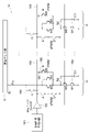
- FIG. 3 is a circuit diagram showing an example of the internal configuration of the signal output unit 18.
- the signal output unit 18 includes a lamp wave generation circuit 181, a voltage follower circuit 182, a switch A, an xPWM switch D, a current holding unit 184, a current control unit 185, a voltage setting unit 186, and a reset unit 188. , Equipped with.
- the lamp wave generation circuit 181 as a reference voltage generation unit generates a reference voltage whose voltage level changes with time in the first period P1 before driving a plurality of signal lines SL.
- the first period P1 is the current sampling period shown in FIG.
- the reference voltage is, for example, a ramp voltage at which the voltage level changes continuously (see FIG. 4).
- the reference voltage is not limited to the lamp wave voltage, and may be any voltage that changes with a substantially constant slope with time.
- the details of the first period P1 will be described later with reference to FIG. In the following, an example in which the lamp wave generation circuit 181 generates a lamp wave voltage whose voltage level changes linearly with time in the first period P1 and generates a voltage whose voltage level is constant in the second period P2. Will be mainly explained.
- the voltage follower circuit 182 is connected between the lamp wave generation circuit 181 and the current holding unit 184, and supplies a reference voltage to the current holding unit 184 during the first period P1.
- the voltage follower circuit 182 outputs a lamp wave voltage to the lamp wiring 180.
- the signal output unit 18 may further include an offset voltage generation circuit (not shown).
- the voltage follower circuit 182 switches between the offset voltage Vofs for correcting the threshold value of the drive transistor 42 in the pixel circuit 15 and the lamp wave voltage at which the voltage level changes continuously, and outputs the voltage to the lamp wiring 180. do.
- a plurality of switches A and a plurality of reset units 188 are connected to the lamp wiring 180.
- the switch A, the xPWM switch D, the current holding unit 184, the current control unit 185, the voltage setting unit 186, and the reset unit 188 are drive units U corresponding to one signal line SL. Therefore, a plurality of drive units U corresponding to the plurality of signal lines SL are connected to the lamp wiring 180. That is, the current holding unit 184 and the current control unit 185 are provided for each of the plurality of signal lines SL.
- Switch A is connected between the lamp wiring 180 and the current control unit 185.
- the xPWM switch D is connected between the switch A, the current control unit 185, and the ground. For example, a signal at a level opposite to the PWM (Pulse Width Modulation) signal input to the transistor M3, which will be described later, is input to the xPWM switch D.
- PWM Pulse Width Modulation
- the current control unit 185 is connected between the signal line SL and the current holding unit 184.
- the current control unit 185 includes a transistor M2 and a transistor M3.
- the transistor M2 is, for example, a p-type MOS transistor.
- the transistor M2 functions as a source follower. That is, the transistor M2 also serves as a part of the current control unit 185 and a buffer unit. The details of the transistor M3 will be described later.
- the gate of the transistor M2 is connected to the lamp wiring 180 via the switch A. Further, the gate of the transistor M2 is connected to the ground via the xPWM switch D. The drain of the transistor M2 is connected to the current holding unit 184, and the source of the transistor M2 is connected to the signal line SL.
- Transistor M3 is provided in parallel with transistor M2.
- the current control unit 185 composed of the transistors M2 and M3 converts the current held by the current holding unit 184 into the corresponding signal line SL according to the logic of the PWM signal having the pulse width corresponding to the time length of the drive period P2. Switch whether to flush or not.
- the PWM signal has a pulse width corresponding to the drive voltage of the corresponding signal line.
- the drive voltage of the signal line SL is the gradation voltage of the pixels driven by the signal line SL
- the PWM signal has a pulse width corresponding to the gradation voltage. That is, the PWM signal has a unique pulse width for each signal line SL.
- the transistors M2 and M3 constituting the current control unit 185 have different conductive types from each other.
- the transistor M2 is a p-type MOS transistor
- the transistor M3 is an n-type MOS transistor.
- Transistors M2 and M3 are turned on or off in synchronization. Further, the transistor M2 constitutes a part of the source follower circuit.
- the current holding unit 184 is provided corresponding to the signal line SL, and holds the current according to the load of the signal line SL and the time change of the reference voltage. That is, the current holding unit 184 holds the current corresponding to the value obtained by multiplying the load of the corresponding signal line by the voltage change value per unit time of the reference voltage.
- the current holding unit 184 holding the current in the first period (current sampling period) P1 functions as a constant current source through which a substantially constant current flows during the driving period (second period) shown in FIG.
- the load of the signal line SL is a parasitic capacitance of the signal line SL, and is a value peculiar to each signal line SL. That is, the load of the signal line SL is a value that can differ for each signal line SL.
- the current held by the current holding unit 184 holds a current whose current level is different for each signal line SL due to the difference in the parasitic capacitance of each signal line SL.
- the current holding unit 184 has a first transistor M1, a second transistor M5, a switch Aa, and a first capacitor C1.
- the first capacitor C1 accumulates electric charges according to the current flowing in P1 during the first period.
- the first capacitor C1 stores an electric charge corresponding to the current output from the lamp wave generation circuit 181 (voltage follower circuit 182).
- the first capacitor C1 is connected between the gate of the first transistor M1 and the switch Aa and the ground.
- the first transistor M1 continuously causes a current to flow through the signal line SL in the second period P2 based on the accumulated charge of the first capacitor C1.
- the second period P2 is a period within the driving period shown in FIG. The details of the second period P2 will be described later with reference to FIG.
- the first transistor M1 is, for example, an n-type MOS transistor.
- the first transistor M1 is connected between the second transistor M5 and ground.
- the gate of the first transistor M1 is connected to the first capacitor C1 and is also connected to the current control unit 185 and the second transistor M5 via the switch Aa.
- the second transistor M5 is cascode connected to the first transistor M1. Further, the second transistor M5 is set to the on state from the first period P1 to the second period P2. The second transistor M5 is used to suppress voltage fluctuations.
- the second transistor M5 is, for example, an n-type MOS transistor.
- the second transistor M5 is connected between the current control unit 185 and the switch Aa, and the first transistor M1.
- the gate of the second transistor M5 is biased to, for example, a voltage at which both the first transistor M1 and the second transistor M5 are turned on.
- the second transistor M5 may be, for example, always on.
- the bias voltage of the second transistor M5 is the same as that of the second transistor M5 with respect to the other signal line SL.
- the switch Aa connects the first transistor M1 to a diode in P1 during the first period.
- the switch Aa is connected between the current control unit 185 and the second transistor M5, and the gate of the first capacitor C1 and the first transistor M1.
- the switch Aa is turned on (closed state)
- the gate of the first transistor M1 and the drain of the first transistor M1 are connected, so that the first transistor M1 is connected by a diode. ..
- the first capacitor C1 stores an electric charge corresponding to the current flowing through the diode-connected first transistor M1. More specifically, the switch Aa accumulates an electric charge in the first capacitor C1 in the first period P1 according to the current flowing through the diode-connected first transistor M1 and the second transistor M5. That is, the first capacitor C1 holds the voltage corresponding to the gate-source voltage of the diode-connected first transistor M1 in the first period P1.
- the current control unit 185 causes a current to flow between the signal line SL and the current holding unit 184 within the second period P2 according to the drive voltage of the signal line SL.
- the load is, as described above, the parasitic capacitance of the signal line SL.
- the transistor M3 which is a part of the current control unit 185, a PWM signal having a pulse width corresponding to the drive voltage of the signal line is input to the gate, and the current holding unit 184 is located between the signal line SL and the current holding unit 184. Pass the current according to the current held by.
- the transistor M3 is, for example, an n-type MOS transistor.
- the transistor M3 is connected between the current holding unit 184 and the signal line SL. That is, the transistor M3 is connected in parallel with the transistor M2.
- the voltage setting unit 186 sets the voltage between the current control unit 185 and the current holding unit 184.
- the voltage setting unit 186 sets, for example, the voltage between the current control unit 185 and the current holding unit 184 to a desired initial voltage. As a result, the current control unit 185 can be operated more appropriately by the PWM signal.
- the voltage setting unit 186 has a transistor M4.
- the transistor M4 is, for example, a p-type MOS transistor.
- the transistor M4 is connected between the power supply and the current holding unit 184 and the current control unit 185.
- the power supply voltage is, for example, about 3V to about 5V.
- the current control unit 185 applies the drive voltage of the signal line SL by passing the current held by the current holding unit 184 to the corresponding signal line SL in the second period P2 after the lapse of the first period P1.
- the load of the signal line SL is a parasitic capacitance of the signal line SL, and is a value peculiar to each signal line SL.
- the drive voltage is a voltage determined by the pulse width of the PWM signal that is different for each signal line SL, and is a voltage that is different for each signal line SL.
- the current holding unit 184 holds the current according to the parasitic capacitance of the signal line SL. Therefore, the current control unit 185 allows the current held in the current holding unit 184 to flow through the signal line SL, so that a drive voltage independent of the parasitic capacitance of each signal line SL can be set in each signal line SL.
- the reset unit 188 resets the voltage of the signal line SL.
- the reset unit 188 has a switch C.
- the switch C is connected between the signal line SL and the lamp wiring 180. When the switch C is turned on, it releases the charge accumulated in the parasitic capacitance of the signal line SL. This resets the signal line voltage.
- FIG. 4 is a timing chart showing an example of the operation of the signal output unit 18.
- the current sampling period (first period P1) is a period in which the current holding unit 184 holds the current via the transistor M2 of the current control unit 185 that functions as a buffer unit.
- the reset period is a period in which the reset unit 188 resets the voltage of the signal line SL in the current sampling period.
- the drive period is a period in which the current control unit 185 generates a drive voltage for the signal line SL by passing a current.
- RAMP indicates the voltage output by the lamp wave generation circuit 181.
- a and Aa indicate an on state or an off state of the switches A and Aa.
- B indicates the gate voltage of the transistor M4 of the voltage setting unit 186. The transistor M4 is turned off when the voltage B is at the H (High) level, and turned on when the voltage B is at the L (Low) level.
- C indicates an on state or an off state of the switch C.
- PWM indicates a PWM signal input to the gate of the transistor M3 of the current control unit 185.
- Pix indicates a voltage (signal line voltage) in the signal line SL.
- the maximum value of the signal line voltage Pix shown in FIG. 4 is, for example, a voltage slightly smaller than the power supply voltage of about 3 V to about 5 V connected to the voltage setting unit 186.
- the minimum value of the signal line voltage Pix shown in FIG. 4 is, for example, about 1V.
- the timing chart shown in FIG. 4 is executed simultaneously on a plurality of signal lines. Further, the pulse width of the PWM signal (second period P2) is different for each signal line. As a result, the signal line is driven by the signal line voltage Pix peculiar to each signal line.
- switch C In the initial state before the current sampling period, switch C is on. Further, the voltage follower circuit 182 outputs a 0 gradation voltage V 0 . Therefore, the signal line voltage Pix of the signal line SL is biased to the 0 gradation voltage V0.
- the voltage follower circuit 182 outputs a lamp wave whose voltage changes with time with a constant slope.
- switches A and Aa are turned on.
- the transistor M2 performs a source follower operation, and the first transistor M1 and the second transistor M5 are connected by a diode.
- Equation 1 Cp ⁇ (dV / dt) (Equation 1)
- the magnitude of the current I is proportional to the slope (dV / dt) of the lamp wave voltage.
- This current I flows through the first transistor M1 together with the signal line SL.
- a gate voltage Vg in which the drain current becomes the current I is generated.
- the signal line voltage Pix shown in FIG. 4 changes due to the current flowing through the signal line SL.
- the gate voltage Vg is set in the first capacitor C1 at the same time for a plurality of signal lines (channels) regardless of variations in the threshold voltage Vth and mobility of the transistors of each signal line.
- This gate voltage Vg can generate a current I that changes each signal line over time with the slope of the ramp wave voltage (dV / dt).
- the current held by the current holding unit 184 depends on the load capacitance Cp, which is the parasitic capacitance of each signal line.
- the current holding unit 184 can suppress the influence of the wiring resistance and the parasitic capacitance of the lamp wiring 180 and hold a substantially constant current in each signal line. As a result, it is not necessary to increase the wiring width in order to reduce the wiring resistance, and the wiring can be mounted in a small area.
- the reset period is a period in which the state in which the lamp wave is written on the signal line voltage Pix in the current sampling period is set to the initial state before the drive period.
- the voltage B becomes the L level and the switch C is turned on.
- the voltage of the lamp wiring 180 and the source voltage and drain voltage of the transistor M2 are set to 0 gradation voltage V0.
- the off timing of the switch A and the L level timing of the voltage B are almost synchronized. However, either timing may be slightly earlier than the other.
- the drive period is an operation of writing a signal voltage (drive voltage) to the signal line SL using a constant current source set in the current sampling period and a PWM signal whose pulse width changes depending on the display data.
- the switch C is turned off, the voltage B becomes the H level, the PWM level becomes the H level, the xPWM level becomes the L level, and then the PWM signal becomes the L level after the lapse of time T according to the display data. And xPWM becomes H level.
- the signal line voltage Pix of V 0 ⁇ (dV / dt) ⁇ T is written in the signal line SL.
- the second period P2 is a time length corresponding to the drive voltage of the signal line SL, and is specified by the pulse width of the PWM signal. Further, the current control unit 185 generates a drive voltage for the signal line SL by continuously passing a current through the signal line SL during the second period P2.
- the second period P2 corresponds to the time T. Therefore, the shorter the second period P2, the higher the signal line voltage Pix. On the other hand, the longer the second period P2, the lower the signal line voltage Pix.
- the current flows from the current holding unit 184 to the signal line SL via the transistors M2 and M3 of the current control unit 185. Therefore, during the drive period, the current output by the ramp wave generation circuit 181 and the voltage follower circuit 182 is not required.
- the voltage follower circuit 182 is an amplifier circuit that requires a bias current. Therefore, it is not necessary to pass the bias current of the voltage follower circuit 182 in the period other than the current sampling period, and only the minimum necessary current for driving the signal line is consumed, so that the power consumption can be suppressed.
- the voltage written on each signal line is set to the current by the operation of the above current sampling period. Therefore, it is possible to suppress the influence of the variation of the current source in the current holding unit 184 and the variation of the parasitic capacitance of the lamp wiring 180, and it is possible to generate the signal line voltage in which the deviation between the signal lines is suppressed.
- FIG. 5 is a timing chart showing an example of the operation of the display device 1.
- the signal line drive circuit 12 generates a drive voltage for all signal lines each time the write scanning unit 16 drives one scan line.
- a plurality of scanning lines are provided in one frame, and a plurality of pixels connected to one scanning line are referred to as one horizontal line (1H).
- FIG. 5 shows a timing chart of a typical signal in a pixel circuit when all the pixels in one frame are driven in order for each horizontal line.
- the signal DS is a gate signal of the light emission control transistor 44.
- the signal AZ is a gate signal of the switching transistor 48.
- the signal WS is a gate signal of the sampling transistor 43.
- the operation of the pixel circuit of FIG. 2 will be described based on the timing chart of FIG. First, at time t1, since the signal AZ transitions from high to low, the switching transistor 48 is turned on and the light emission of the light emitting unit 41 is stopped. Further, the sampling transistor 43 is turned on, and the offset voltage Vofs on the signal line is supplied to one end of the holding capacity 45. At this time, the light emission control transistor 44 is turned on, and the power supply voltage Vcc is supplied to the other end of the holding capacity 45. Therefore, a voltage of (Vcc-Vofs) is applied to both ends of the holding capacity 45.
- the light emission control transistor 44 is turned off. As a result, a part of the electric charge accumulated in the holding capacity 45 is transferred to the auxiliary capacity 46, and the electric charge is distributed. Specifically, the electric charge corresponding to the threshold voltage of the drive transistor 42 is accumulated in the holding capacity 45.
- the sampling transistor 43 turns off. After that, at time t4, the signal line voltage Vsig is supplied on the signal line. After that, at time t5, the sampling transistor 43 is turned on, and the signal line voltage Vsig is supplied to the gate of the drive transistor 42. Since the holding capacitance 45 corrects the threshold voltage of the drive transistor 42, an offset-corrected and threshold-corrected voltage is applied between the gate and the source of the drive transistor 42 with respect to the signal line voltage Vsig. ..
- the light emission control transistor 44 is turned on, the switching transistor 48 is turned off, a voltage corresponding to the signal line voltage Vsig is applied to the anode of the light emitting unit 41, and light emission corresponding to the anode voltage is applied.
- the light emitting unit 41 emits light with brightness.
- the operations of the current sampling period, the reset period, and the drive period are executed for each horizontal line (1H) which is the rewrite period. This is because the current value is stored in the first capacitor C1, so that the signal line voltage may shift due to switch noise due to one drive.
- lamp wave drive for current sampling and the writing of the offset voltage Vofs may be used in combination.
- the ramp wave generation circuit 181 generates a reference voltage (ramp wave voltage) whose voltage level changes with time. Further, the current holding unit 184 provided corresponding to the signal line SL holds the current according to the time change of the lamp wave voltage.
- a current mirror circuit As another method of duplicating the current value, for example, a current mirror circuit is known.
- variations in current may occur due to variations in the element characteristics of the transistor.
- variations in signal line voltage occur between signal lines due to variations in parasitic capacitance for each signal line.
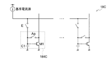
- FIG. 6 is a circuit diagram showing an example of the internal configuration of the signal output unit 18C and the current holding unit 184C according to a comparative example.
- FIG. 6 is a diagram illustrating a current sampling circuit as another method of replicating the current value.
- a reference current source is provided in place of the lamp wave generation circuit 181.
- the current holding unit 184C shown in FIG. 6 may be substantially the same as the current holding unit 184 shown in FIG. In the example shown in FIG. 6, the current holding unit 184C is connected to the reference current source via the switch E on the current input side. The current holding unit 184C is connected to the transistor M3 (not shown) of the current control unit 185 on the current output side.
- the current sampling circuit shown in FIG. 6 can duplicate the current of the reference current source with high accuracy. However, it is difficult to duplicate the current for a plurality of signal lines at the same time. Therefore, it is necessary to replicate the current of the reference current source one by one to the current holding unit 184C in each signal line, which takes time. Also, the higher the definition panel, the longer it will take to replicate the current. Further, as in the current mirror circuit, variations in signal line voltage occur between signal lines due to variations in parasitic capacitance for each signal line. It was
- the plurality of current holding units 184 hold the current output from the lamp wave generation circuit 181 in parallel.
- a plurality of current holding units 184 are provided corresponding to the plurality of signal line SLs. Therefore, the current value of the constant current source can be set by simultaneously voltage-driving all the signal lines (channels) with the lamp waveform and simultaneously performing current sampling on each signal line for the current flowing at that time. .. As a result, the current can be duplicated for a plurality of signal lines at the same time, and the current can be set with higher accuracy and in a shorter time.
- the current value of the constant current source is a current value corresponding to the parasitic capacitance value of each signal line.
- the lamp wave voltage changes to the negative side.
- the present invention is not limited to this, and the ramp wave voltage may change to the positive side.
- the transistors M1 to M5 shown in FIG. 3 may be MOS transistors having opposite polarities.
- FIG. 7 is a flow chart showing an example of the operation of the signal output unit 18 according to the modified example.
- the modification is different from the first embodiment in that the operation during the current sampling period is not executed for each horizontal line (every H).
- the reset period (S20) and the drive period (S30) are repeated after the current sampling period (S10).
- a common current value obtained by one operation in the current sampling period (S10) is used.
- the operations of the reset period (S20) and the drive period (S30) are repeatedly executed for each horizontal line as in the first embodiment.
- the drive period may be executed a plurality of times after the current is set. Since the operation during the current sampling period consumes a large amount of power, the power consumption can be further suppressed by reducing the number of times during the current sampling period.
- the other configurations of the signal line drive circuit 12 according to the modified example are the same as the corresponding configurations of the signal line drive circuit 12 according to the first embodiment, detailed description thereof will be omitted.
- the signal line drive circuit 12 according to the modified example can obtain the same effect as that of the first embodiment.
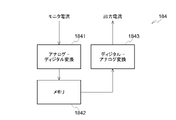
- FIG. 8 is a block diagram showing an example of the configuration of the current holding unit 184 according to the second embodiment.
- the current holding unit 184 has an ADC (Analog to Digital Converter) 1841, a memory 1842, and a DAC (Digital to Analog Converter) 1843.
- ADC Analog to Digital Converter
- memory 1842 a memory 1842
- DAC Digital to Analog Converter
- the ADC 184 as an analog-to-digital converter converts the current corresponding to the time change of the reference voltage into a digital value.
- the memory 1842 as a current storage unit stores a digital value.
- the memory 1842 may be, for example, a volatile memory such as a SRAM (Static Random Access Memory) and a latch.
- the DAC1843 as a digital-to-analog conversion unit converts the digital value stored in the memory 1842 into an electric current.
- the current control unit 185 generates a drive voltage for the signal line SL by passing the current converted by the DAC 1843 to the corresponding signal line SL. More specifically, the current control unit 185 generates the drive voltage of the signal line SL based on the current converted by the DAC 1843 and the time length of the drive period (second period) P2.
- the first capacitor C1 can be omitted, and the fluctuation of the set current due to the leakage of the first capacitor C1 can be suppressed. That is, it is possible to suppress the influence of noise generated by one drive described in the first embodiment.
- the operation during the current sampling period does not have to be executed for each horizontal line (every H), and may be executed, for example, in frame units.
- the other configurations of the signal line drive circuit 12 according to the second embodiment are the same as the corresponding configurations of the signal line drive circuit 12 according to the first embodiment, detailed description thereof will be omitted.
- the signal line drive circuit 12 according to the second embodiment can obtain the same effect as that of the first embodiment. Further, a modification may be combined with the signal line drive circuit 12 according to the second embodiment.
- the present technology can have the following configurations.
- a signal line drive circuit that drives a plurality of signal lines.
- a reference voltage generation unit that generates a reference voltage whose voltage level changes with time within the first period before driving the plurality of signal lines.
- a current holding unit provided corresponding to the signal line and holding a current corresponding to the load of the signal line and the time change of the reference voltage.
- a current control unit that generates a drive voltage of the signal line by passing a current held by the current holding unit to the corresponding signal line is provided.
- Signal line drive circuit (2) The signal line drive circuit according to (1), wherein the current holding unit and the current control unit are provided for each of the plurality of signal lines.
- the current holding unit holds a current corresponding to the value obtained by multiplying the load of the corresponding signal line by the voltage change value per unit time of the reference voltage, according to (1) or (2).
- the reference voltage generation unit generates the reference voltage whose voltage level changes linearly with time within the first period, and generates the reference voltage whose voltage level is constant within the second period.
- the second period has a time length peculiar to each signal line.
- the item according to any one of (1) to (4), wherein the current control unit generates a drive voltage of the signal line by continuously flowing the current through the signal line within the second period.
- the current control unit transfers the current held by the current holding unit to the corresponding signal line according to the logic of the pulse width modulation signal having the pulse width corresponding to the time length of the second period.
- the signal line drive circuit according to any one of (3) to (5), which switches whether or not to flow.
- the signal line drive circuit according to (6), wherein the pulse width modulated signal has a pulse width corresponding to the drive voltage of the corresponding signal line.
- the drive voltage of the signal line is the gradation voltage of the pixel driven by the signal line.
- the signal line drive circuit according to (7), wherein the pulse width modulation signal has a pulse width corresponding to the gradation voltage.
- the current holding unit is A first capacitor that stores an electric charge corresponding to the current flowing in the first period, The item according to any one of (5) to (10), comprising a first transistor that continuously causes the current to flow through the signal line within the second period based on the accumulated charge of the first capacitor. Signal line drive circuit. (12) The current holding unit further has a switch for diode-connecting the first transistor within the first period.
- the current holding unit further includes a second transistor cascode-connected to the first transistor. The second transistor is set to the on state from the first period to the second period.
- the current holding unit is An analog-to-digital conversion unit that converts the current according to the time change of the reference voltage into a digital value, and A current storage unit that stores the digital value and It has a digital-analog conversion unit that converts the digital value stored in the current storage unit into the current.
- the current control unit generates a drive voltage for the signal line by passing the current converted by the digital-to-analog conversion unit to the corresponding signal line, whichever is one of (1) to (10).
- a plurality of the current holding portions are provided corresponding to the plurality of signal lines.
- the signal line drive circuit according to any one of (1) to (14), wherein the plurality of current holding units hold the current output from the reference voltage generating unit in parallel.
- the signal line drive circuit according to any one of the items.
- (1) to (16) include an initial voltage setting unit for setting the signal line to a predetermined reference voltage within the third period from the lapse of the first period to the start of the second period. ) Is described in any one of the signal line drive circuits.
Landscapes
- Engineering & Computer Science (AREA)
- Physics & Mathematics (AREA)
- Computer Hardware Design (AREA)
- General Physics & Mathematics (AREA)
- Theoretical Computer Science (AREA)
- Control Of Indicators Other Than Cathode Ray Tubes (AREA)
Abstract
[課題]信号線電圧のばらつきを抑制する。 [解決手段]信号線駆動回路は、複数の信号線を駆動する信号線駆動回路であって、前記複数の信号線を駆動する前の第1期間内において、電圧レベルが時間に応じて変化する基準電圧を生成する基準電圧生成部と、前記信号線に対応して設けられ、前記信号線の負荷と前記基準電圧の時間変化とに応じた電流を保持する電流保持部と、前記第1期間の経過後の第2期間内に、前記電流保持部が保持する電流を対応する前記信号線に流すことにより、前記信号線の駆動電圧を生成する電流制御部と、を備える。
Description
本開示による実施形態は、信号線駆動回路に関する。
ディスプレイ等では、複数の画素回路を駆動する信号線駆動回路が用いられる。信号線駆動回路では、複数のボルテージフォロア回路で信号線を駆動する方式が広く用いられている。しかし、この方式では、アンプ回路を含むボルテージフォロア回路にバイアス電流を流す必要があり、消費電力が増大するという問題がある。
このバイアス電流を削減するために、定電流源を用いて、表示データ(信号電圧)に応じた期間、容量負荷に一定電流を流すことにより、所望の信号線電圧で複数の画素回路を駆動する方式が提案されている(特許文献1参照)。
しかし、この方式では、例えば、定電流源となるトランジスタの移動度等の特性ばらつきに起因する電流ばらつきによって、書き込み電圧のばらつきが生じてしまう問題がある。また、このような書き込み電圧(信号線電圧)のばらつきによって、例えば、ディスプレイの表示品質が低下する問題もある。
そこで、本開示では、信号線電圧のばらつきを抑制することができる信号線駆動回路を提供するものである。
上記の課題を解決するために、本開示によれば、
複数の信号線を駆動する信号線駆動回路であって、
前記複数の信号線を駆動する前の第1期間内において、電圧レベルが時間に応じて変化する基準電圧を生成する基準電圧生成部と、
前記信号線に対応して設けられ、前記信号線の負荷と前記基準電圧の時間変化とに応じた電流を保持する電流保持部と、
前記第1期間の経過後の第2期間内に、前記電流保持部が保持する電流を対応する前記信号線に流すことにより、前記信号線の駆動電圧を生成する電流制御部と、を備える、信号線駆動回路が提供される。
複数の信号線を駆動する信号線駆動回路であって、
前記複数の信号線を駆動する前の第1期間内において、電圧レベルが時間に応じて変化する基準電圧を生成する基準電圧生成部と、
前記信号線に対応して設けられ、前記信号線の負荷と前記基準電圧の時間変化とに応じた電流を保持する電流保持部と、
前記第1期間の経過後の第2期間内に、前記電流保持部が保持する電流を対応する前記信号線に流すことにより、前記信号線の駆動電圧を生成する電流制御部と、を備える、信号線駆動回路が提供される。
前記電流保持部及び前記電流制御部は、前記複数の信号線のそれぞれごとに設けられてもよい。
前記電流保持部は、対応する前記信号線の前記負荷に、前記基準電圧の単位時間当たりの電圧変化値を乗じた値に応じた電流を保持してもよい。
前記基準電圧生成部は、前記第1期間内では時間に応じて線形に電圧レベルが変化する前記基準電圧を生成し、前記第2期間内では電圧レベルが一定の前記基準電圧を生成してもよい。
前記第2期間は、個々の前記信号線に固有の時間長さを有し、
前記電流制御部は、前記第2期間内に前記信号線に前記電流を継続して流すことにより、前記信号線の駆動電圧を生成してもよい。
前記電流制御部は、前記第2期間内に前記信号線に前記電流を継続して流すことにより、前記信号線の駆動電圧を生成してもよい。
前記電流制御部は、前記第2期間の時間長さに応じたパルス幅を有するパルス幅変調信号の論理に応じて、前記電流保持部で保持された電流を対応する前記信号線に流すか否かを切り替えてもよい。
前記パルス幅変調信号は、対応する前記信号線の駆動電圧に応じたパルス幅を有してもよい。
前記信号線の駆動電圧は、前記信号線にて駆動される画素の階調電圧であり、
前記パルス幅変調信号は、前記階調電圧に応じたパルス幅を有してもよい。
前記パルス幅変調信号は、前記階調電圧に応じたパルス幅を有してもよい。
前記電流制御部は、導電型が互いに異なり、互いに同期してオン又はオフする並列接続された2つのトランジスタを有してもよい。
前記2つのトランジスタのうち一方は、ソースフォロワ回路の一部を構成してもよい。
前記電流保持部は、
前記第1期間内に流れる前記電流に応じた電荷を蓄積する第1キャパシタと、
前記第1キャパシタの蓄積電荷に基づいて、前記第2期間内に前記信号線に前記電流を継続して流す第1トランジスタと、を有してもよい。
前記第1期間内に流れる前記電流に応じた電荷を蓄積する第1キャパシタと、
前記第1キャパシタの蓄積電荷に基づいて、前記第2期間内に前記信号線に前記電流を継続して流す第1トランジスタと、を有してもよい。
前記電流保持部は、前記第1期間内に前記第1トランジスタをダイオード接続させるスイッチをさらに有し、
前記第1キャパシタは、ダイオード接続された前記第1トランジスタを流れる前記電流に応じた電荷を蓄積してもよい。
前記第1キャパシタは、ダイオード接続された前記第1トランジスタを流れる前記電流に応じた電荷を蓄積してもよい。
前記電流保持部は、前記第1トランジスタにカスコード接続された第2トランジスタをさらに有し、
前記第2トランジスタは、前記第1期間から前記第2期間にかけてオン状態に設定され、
前記スイッチは、前記第1期間内に、ダイオード接続された前記第1トランジスタ及び前記第2トランジスタを流れる電流に応じた電荷を前記第1キャパシタに蓄積してもよい。
前記第2トランジスタは、前記第1期間から前記第2期間にかけてオン状態に設定され、
前記スイッチは、前記第1期間内に、ダイオード接続された前記第1トランジスタ及び前記第2トランジスタを流れる電流に応じた電荷を前記第1キャパシタに蓄積してもよい。
前記電流保持部は、
前記基準電圧の時間変化に応じた前記電流をデジタル値に変換するアナログ-デジタル変換部と、
前記デジタル値を記憶する電流記憶部と、
前記電流記憶部に記憶される前記デジタル値を前記電流に変換するデジタル-アナログ変換部と、を有し、
前記電流制御部は、前記デジタル-アナログ変換部で変換された前記電流を対応する前記信号線に流すことにより、前記信号線の駆動電圧を生成してもよい。
前記基準電圧の時間変化に応じた前記電流をデジタル値に変換するアナログ-デジタル変換部と、
前記デジタル値を記憶する電流記憶部と、
前記電流記憶部に記憶される前記デジタル値を前記電流に変換するデジタル-アナログ変換部と、を有し、
前記電流制御部は、前記デジタル-アナログ変換部で変換された前記電流を対応する前記信号線に流すことにより、前記信号線の駆動電圧を生成してもよい。
前記複数の信号線に対応して、複数の前記電流保持部が設けられ、
前記複数の電流保持部は、前記基準電圧生成部から出力される電流を並行して保持してもよい。
前記複数の電流保持部は、前記基準電圧生成部から出力される電流を並行して保持してもよい。
前記基準電圧生成部と前記電流保持部との間に接続され、前記第1期間内に前記基準電圧を前記電流保持部に供給するボルテージフォロア回路をさらに備えてもよい。
前記第1期間が経過してから前記第2期間が始まるまでの第3期間内に、前記信号線を所定の基準電圧に設定する初期電圧設定部を備えてもよい。
前記負荷は、個々の前記信号線の寄生容量であってもよい。
以下、図面を参照して、信号線駆動回路の実施形態について説明する。以下では、信号線駆動回路の主要な構成部分を中心に説明するが、信号線駆動回路には、図示又は説明されていない構成部分や機能が存在しうる。以下の説明は、図示又は説明されていない構成部分や機能を除外するものではない。
また、図面は模式的または概念的なものであり、各部分の比率などは、必ずしも現実のものと同一とは限らない。明細書と図面において、既出の図面に関して前述したものと同様の要素には同一の符号を付して詳細な説明は適宜省略する。
(第1実施形態)
図1は、第1実施形態による表示装置1の概略構成を示すブロック図である。図1の表示装置1は、例えば、有機EL(Electroluminescence)素子(以下では、OLED:Organic Light Emitting Diodeとも呼ぶ)等の発光素子を有する表示装置である。しかし、これに限られず、表示装置1は、他の表示装置であってもよい。
図1は、第1実施形態による表示装置1の概略構成を示すブロック図である。図1の表示装置1は、例えば、有機EL(Electroluminescence)素子(以下では、OLED:Organic Light Emitting Diodeとも呼ぶ)等の発光素子を有する表示装置である。しかし、これに限られず、表示装置1は、他の表示装置であってもよい。
表示装置1は、画素アレイ部11と、信号線SLと、信号線駆動回路12と、を備える。
画素アレイ部11は、水平方向及び垂直方向に配置される複数の画素回路15を有する。各画素回路15は、例えば有機EL素子等の発光部と、発光部を制御する複数のトランジスタと、複数の容量とを有する。画素回路15の内部構成は後述する。
信号線駆動回路12は、複数の信号線SLを駆動する。図1に示す信号線駆動回路12は、表示装置1に設けられ、画素回路15の信号線SLの駆動に用いられる。しかし、これに限られず、信号線駆動回路12は、他の信号線の駆動に用いられてもよい。信号線駆動回路12は、例えば、複数の信号線を駆動させる装置に用いられることが好ましい。
信号線駆動回路12は、画素アレイ部11に表示されるべき映像信号の信号処理を行ってもよい。信号処理の具体的内容は問わないが、例えばガンマ補正などである。
信号線駆動回路12は、後述する図2に示すように、書き込み走査部16と、駆動走査部17と、信号出力部18と、を有する。
書き込み走査部16は、各画素回路15に信号電圧を書き込むに際して、各走査線に書き込み走査信号を順次供給して、各走査線WS1~WSnを順次駆動する。
駆動走査部17は、書き込み走査部16による線順次走査に同期して、各駆動線に発光制御信号を供給し、発光部の発光と非発光を制御する。
信号出力部18は、ランプ波電圧を、各画素の階調に応じたタイミングで保持して信号電圧を生成する。信号出力部18は、信号電圧又はオフセット電圧Vofsを選択的に選択して、対応する信号線SLに供給する。オフセット電圧Vofsは、信号電圧の基準となる電圧(例えば、映像信号の黒レベルに相当する電圧)であり、後述する閾値補正動作を行うために用いられる。
信号出力部18から択一的に出力される信号電圧又はオフセット電圧Vofsは、信号線SLを介して各画素回路15に供給され、書き込み走査部16による走査で選択された行単位で、各画素回路15に設定される。
図2は、画素回路15の内部構成の一例を示す回路図である。図2の画素回路15は、有機EL素子を有する発光部41と、駆動トランジスタ42と、サンプリングトランジスタ43と、発光制御トランジスタ44と、保持容量(キャパシタ)45と、補助容量(キャパシタ)46とを有する。画素回路15は、シリコン等の半導体基板上に形成され、駆動トランジスタ42、サンプリングトランジスタ43及び発光制御トランジスタ44は例えばPMOS(Metal Oxide Semiconductor)トランジスタである。各トランジスタはバックゲートには電源電圧が印加されている。
サンプリングトランジスタ43は、信号出力部18から信号線SLを介して供給されるオフセット電圧Vofs又は信号線電圧Vsigをサンプリングすることによって保持容量45に書き込む。発光制御トランジスタ44は、電源電圧Vccの電源ノードと駆動トランジスタ42のソース電極との間に接続され、発光制御信号DSによる駆動の下に、発光部41の発光/非発光を制御する。
保持容量45は、駆動トランジスタ42のゲート電極とソース電極との間に接続されている。この保持容量45は、サンプリングトランジスタ43によるサンプリングによって書き込まれた信号線電圧Vsigを保持する。駆動トランジスタ42は、保持容量45の保持電圧に応じた駆動電流を発光部41に流すことによって発光部41を駆動する。補助容量46は、駆動トランジスタ42のソース電極と、固定電位のノード、例えば、電源電圧Vccの電源ノードとの間に接続されている。この補助容量46は、信号線電圧Vsigを書き込んだときに駆動トランジスタ42のソース電位が変動するのを抑制するとともに、駆動トランジスタ42のゲート-ソース間電圧Vgsを駆動トランジスタ42の閾値電圧Vthに合わせる作用を行う。
スイッチングトランジスタ48は、発光部41の発光を制御する。スイッチングトランジスタ48のゲートには、信号AZが入力されており、信号AZの論理により、スイッチングトランジスタ48はオン又はオフする。スイッチングトランジスタ48がオンの間は、発光部41は発光を停止する。スイッチングトランジスタ48は、駆動トランジスタ42の閾値電圧とオフセット電圧の補正を行っている期間内はオンしており、閾値電圧オフセット電圧の補正が終わるとオフし、発光部41の発光が行われる。
図3は、信号出力部18の内部構成の一例を示す回路図である。
信号出力部18は、ランプ波生成回路181と、ボルテージフォロア回路182と、スイッチAと、xPWMスイッチDと、電流保持部184と、電流制御部185と、電圧設定部186と、リセット部188と、を備える。
基準電圧生成部としてのランプ波生成回路181は、複数の信号線SLを駆動する前の第1期間P1内において、電圧レベルが時間に応じて変化する基準電圧を生成する。第1期間P1は、図4に示すカレントサンプリング期間である。基準電圧は、例えば、電圧レベルが連続的に変化するランプ波電圧である(図4を参照)。基準電圧は、ランプ波電圧に限られず、時間に応じて略一定の傾きで変化する電圧であればよい。なお、第1期間P1の詳細については、図4を参照して、後で説明する。以下では、ランプ波生成回路181が、第1期間P1内では時間に応じて線形に電圧レベルが変化するランプ波電圧を生成し、第2期間P2内では電圧レベルが一定の電圧を生成する例を主に説明する。
ボルテージフォロア回路182は、ランプ波生成回路181と電流保持部184との間に接続され、第1期間P1内に基準電圧を電流保持部184に供給する。ボルテージフォロア回路182は、ランプ配線180にランプ波電圧を出力する。
なお、信号出力部18は、オフセット電圧生成回路(図示せず)をさらに備えていてもよい。この場合、ボルテージフォロア回路182は、画素回路15内の駆動トランジスタ42の閾値補正を行うためのオフセット電圧Vofsと、電圧レベルが連続的に変化するランプ波電圧と、を切り替えてランプ配線180に出力する。
ランプ配線180には、複数のスイッチAと、複数のリセット部188と、が接続されている。スイッチA、xPWMスイッチD、電流保持部184、電流制御部185、電圧設定部186及びリセット部188は、1つの信号線SLに対応する駆動ユニットUである。従って、ランプ配線180には、複数の信号線SLに対応する複数の駆動ユニットUが接続されている。すなわち、電流保持部184及び電流制御部185は、複数の信号線SLのそれぞれごとに設けられる。
スイッチAは、ランプ配線180と電流制御部185との間に接続される。
xPWMスイッチDは、スイッチA及び電流制御部185と、グランドと、の間に接続される。xPWMスイッチDには、例えば、後で説明するトランジスタM3に入力されるPWM(Pulse Width Modulation)信号とは反対のレベルの信号が入力される。
電流制御部185は、信号線SLと電流保持部184との間に接続されている。電流制御部185は、トランジスタM2と、トランジスタM3と、を有する。トランジスタM2は、例えば、p型MOSトランジスタである。トランジスタM2は、ソースフォロアとして機能する。すなわち、トランジスタM2は、電流制御部185の一部とバッファ部とを兼ねる。なお、トランジスタM3の詳細については、後で説明する。
トランジスタM2のゲートは、スイッチAを介してランプ配線180と接続されている。また、トランジスタM2のゲートは、xPWMスイッチDを介してグランドと接続される。トランジスタM2のドレインは、電流保持部184と接続され、トランジスタM2のソースは、信号線SLと接続される。
トランジスタM2に並列にトランジスタM3が設けられている。トランジスタM2とM3からなる電流制御部185は、駆動期間P2の時間長さに応じたパルス幅を有するPWM信号の論理に応じて、電流保持部184で保持された電流を対応する信号線SLに流すか否かを切り替える。PWM信号は、対応する信号線の駆動電圧に応じたパルス幅を有する。より具体的な一例では、信号線SLの駆動電圧は、信号線SLにて駆動される画素の階調電圧であり、PWM信号は、階調電圧に応じたパルス幅を有する。すなわち、PWM信号は、信号線SLごとに固有のパルス幅を有する。
電流制御部185を構成するトランジスタM2、M3は互いに異なる導電型を有する。例えば、トランジスタM2はp型MOSトランジスタであり、トランジスタM3はn型MOSトランジスタである。トランジスタM2、M3は、同期してオン又はオフする。また、トランジスタM2は、ソースフォロワ回路の一部を構成している。
電流保持部184は、信号線SLに対応して設けられ、信号線SLの負荷と基準電圧の時間変化とに応じた電流を保持する。すなわち、電流保持部184は、対応する信号線の負荷に、基準電圧の単位時間当たりの電圧変化値を乗じた値に応じた電流を保持する。第1期間(カレントサンプリング期間)P1において電流を保持した電流保持部184は、図4に示す駆動期間(第2期間)において、略一定の電流を流す定電流源として機能する。ここで、信号線SLの負荷とは、信号線SLの寄生容量であり、信号線SLごとに固有の値である。すなわち、信号線SLの負荷は、信号線SLごとに異なりうる値である。基準電圧が、時間に応じて電圧レベルが線形に変化するランプ波電圧の場合、基準電圧の電圧変化は一定値になる。よって、電流保持部184が保持する電流は、信号線SLごとに、各信号線SLの寄生容量の違いにより電流レベルが異なる電流を保持する。
電流保持部184は、第1トランジスタM1と、第2トランジスタM5と、スイッチAaと、第1キャパシタC1と、を有する。
第1キャパシタC1は、第1期間P1内に流れる電流に応じた電荷を蓄積する。第1キャパシタC1は、ランプ波生成回路181(ボルテージフォロア回路182)から出力される電流に応じた電荷を蓄積する。
第1キャパシタC1は、第1トランジスタM1のゲート及びスイッチAaとグランドとの間に接続される。
第1トランジスタM1は、第1キャパシタC1の蓄積電荷に基づいて、第2期間P2内に信号線SLに電流を継続して流す。第2期間P2は、図4に示す駆動期間内の期間である。なお、第2期間P2の詳細については、図4を参照して、後で説明する。第1トランジスタM1は、例えば、n型MOSトランジスタである。
第1トランジスタM1は、第2トランジスタM5とグランドとの間に接続される。第1トランジスタM1のゲートは、第1キャパシタC1と接続され、また、スイッチAaを介して電流制御部185及び第2トランジスタM5と接続される。
第2トランジスタM5は、第1トランジスタM1にカスコード接続される。また、第2トランジスタM5は、第1期間P1から第2期間P2にかけてオン状態に設定される。第2トランジスタM5は、電圧の変動を抑制するために用いられる。第2トランジスタM5は、例えば、n型MOSトランジスタである。
第2トランジスタM5は、電流制御部185及びスイッチAaと、第1トランジスタM1と、の間に接続されている。第2トランジスタM5は、例えば、第1トランジスタM1及び第2トランジスタM5の両方がオンする電圧にゲートがバイアスされている。第2トランジスタM5は、例えば、常時、オン状態でよい。第2トランジスタM5のバイアス電圧は、他の信号線SLに対する第2トランジスタM5も同様である。
スイッチAaは、第1期間P1内に第1トランジスタM1をダイオード接続させる。
スイッチAaは、電流制御部185及び第2トランジスタM5と、第1キャパシタC1及び第1トランジスタM1のゲートと、の間に接続されている。スイッチAaがオン(閉状態)になると、第1トランジスタM1のゲートと第1トランジスタM1のドレイン(第2トランジスタM5のドレイン)との間が接続されるため、第1トランジスタM1がダイオード接続される。
また、より詳細には、第1キャパシタC1は、ダイオード接続された第1トランジスタM1を流れる電流に応じた電荷を蓄積する。また、より詳細には、スイッチAaは、第1期間P1内に、ダイオード接続された第1トランジスタM1及び第2トランジスタM5を流れる電流に応じた電荷を第1キャパシタC1に蓄積する。すなわち、第1キャパシタC1は、第1期間P1において、ダイオード接続される第1トランジスタM1のゲート-ソース間電圧に対応する電圧を保持する。
電流制御部185は、信号線SLの駆動電圧に応じた第2期間P2内に、信号線SLと電流保持部184との間に電流を流す。負荷は、上述したように、信号線SLの寄生容量である。
電流制御部185の一部であるトランジスタM3は、信号線の駆動電圧に応じたパルス幅を有するPWM信号がゲートに入力され、信号線SLと電流保持部184との間に、電流保持部184が保持する電流に応じた電流を流す。トランジスタM3は、例えば、n型MOSトランジスタである。
トランジスタM3は、電流保持部184と信号線SLとの間に接続されている。すなわち、トランジスタM3は、トランジスタM2と並列に接続されている。
電圧設定部186は、電流制御部185と、電流保持部184と、の間の電圧を設定する。電圧設定部186は、例えば、電流制御部185と、電流保持部184と、の間の電圧を所望の初期電圧に設定する。これにより、PWM信号によって電流制御部185をより適切に動作させることができる。
電圧設定部186は、トランジスタM4を有する。トランジスタM4は、例えば、p型MOSトランジスタである。
トランジスタM4は、電源と、電流保持部184及び電流制御部185と、の間に接続される。電源電圧は、例えば、約3V~約5Vである。トランジスタM4は、リセット部188とともに、第1期間P1が経過してから駆動期間(第2期間)P2が始まるまでの第3期間内に、信号線SLを所定の基準電圧(例えば電源電圧)に設定する初期電圧設定部を構成している。
ここで、電流制御部185は、第1期間P1の経過後の第2期間P2内に、電流保持部184が保持する電流を対応する信号線SLに流すことにより、信号線SLの駆動電圧を生成する。信号線SLの負荷は、上述したように、信号線SLの寄生容量であり、信号線SLごとに固有の値である。駆動電圧は、信号線SLごとに異なるPWM信号のパルス幅によって決まる電圧であり、信号線SLごとに異なる電圧である。
電流保持部184は、信号線SLの寄生容量に応じた電流を保持する。このため、電流制御部185が電流保持部184に保持された電流を信号線SLに流すことで、各信号線SLの寄生容量に依存しない駆動電圧を各信号線SLに設定できる。
リセット部188は、信号線SLの電圧をリセットする。リセット部188は、スイッチCを有する。
スイッチCは、信号線SLとランプ配線180との間に接続される。スイッチCは、オン状態になると、信号線SLの寄生容量に蓄積される電荷を放出させる。これにより、信号線電圧がリセットされる。
次に、信号出力部18の動作について説明する。
図4は、信号出力部18の動作の一例を示すタイミングチャートである。
カレントサンプリング期間(第1期間P1)は、バッファ部として機能する電流制御部185のトランジスタM2を介して、電流保持部184が電流を保持する期間である。リセット期間は、カレントサンプリング期間において信号線SLの電圧を、リセット部188がリセットする期間である。駆動期間は、電流制御部185が電流を流すことにより、信号線SLの駆動電圧を生成する期間である。
RAMPは、ランプ波生成回路181が出力する電圧を示す。A、Aa、は、スイッチA、Aaのオン状態又はオフ状態を示す。Bは、電圧設定部186のトランジスタM4のゲート電圧を示す。なお、トランジスタM4は、電圧BがH(High)レベルの場合にオフ状態となり、電圧BがL(Low)レベルの場合にオン状態となる。Cは、スイッチCのオン状態又はオフ状態を示す。PWMは、電流制御部185のトランジスタM3のゲートに入力されるPWM信号を示す。Pixは、信号線SLにおける電圧(信号線電圧)を示す。図4に示す信号線電圧Pixの最大値は、例えば、電圧設定部186と接続される電源電圧である約3V~約5Vよりわずかに小さい電圧である。図4に示す信号線電圧Pixの最小値は、例えば、約1Vである。
図4に示すタイミングチャートは、複数の信号線において同時に実行される。また、信号線ごとに、PWM信号のパルス幅(第2期間P2)が異なっている。これにより、信号線は、信号線ごとに固有の信号線電圧Pixで駆動される。
カレントサンプリング期間の前の初期状態では、スイッチCがオンである。また、ボルテージフォロア回路182は、0階調電圧V0を出力する。従って、信号線SLの信号線電圧Pixは、0階調電圧V0にバイアスされる。
次に、スイッチCがオフになった後、ボルテージフォロア回路182は、一定の傾きで電圧が時間変化するランプ波を出力する。また、スイッチA、Aaがオンになる。これにより、トランジスタM2は、ソースフォロア動作を行い、第1トランジスタM1及び第2トランジスタM5はダイオード接続となる。
ここで、ランプ波の電圧が時間dtに対してdV変化する場合、信号線の負荷容量をCpとすると、トランジスタM2に流れる電流Iは、式1により表される。
I=Cp×(dV/dt) (式1)
電流Iの大きさは、ランプ波電圧の傾き(dV/dt)に比例している。この電流Iは、信号線SLとともに第1トランジスタM1に流れる。第1トランジスタM1のゲート電圧には、ドレイン電流が電流Iとなるゲート電圧Vgが発生する。なお、信号線SLに流れる電流により、図4に示す信号線電圧Pixが変化している。
I=Cp×(dV/dt) (式1)
電流Iの大きさは、ランプ波電圧の傾き(dV/dt)に比例している。この電流Iは、信号線SLとともに第1トランジスタM1に流れる。第1トランジスタM1のゲート電圧には、ドレイン電流が電流Iとなるゲート電圧Vgが発生する。なお、信号線SLに流れる電流により、図4に示す信号線電圧Pixが変化している。
次に、スイッチA、Aaが順次オフになると、第1トランジスタM1のゲート電圧Vgが第1キャパシタC1に保持される。
以上の動作により、複数の信号線(チャネル)に対して同時に、各信号線のトランジスタの閾値電圧Vth及び移動度等のばらつきによらず、第1キャパシタC1にゲート電圧Vgが設定される。このゲート電圧Vgは、各信号線をランプ波電圧の傾き(dV/dt)で時間変化させる電流Iを発生させることができる。なお、式1に示すように、電流保持部184が保持する電流は、各信号線の寄生容量である負荷容量Cpに依存する。
また、各信号線におけるランプ波電圧には、ランプ配線180の配線抵抗及び寄生容量により、ボルテージフォロア回路182から各信号線までの距離に応じて遅延及び電圧差が発生する場合がある。しかし、ランプ波電圧の傾き自体は場所によらず略一定である。従って、電流保持部184は、ランプ配線180の配線抵抗及び寄生容量の影響を抑制して、各信号線で略一定の電流を保持することができる。この結果、配線抵抗を下げるために配線幅を太くする必要がなく、小面積で実装できる。
リセット期間は、カレントサンプリング期間で信号線電圧Pixにランプ波が書かれた状態を駆動期間の前に初期状態に設定する期間である。
まず、電圧BがLレベルになり、スイッチCがオンになる。これにより、ランプ配線180の電圧、並びに、トランジスタM2のソース電圧及びドレイン電圧が0階調電圧V0に設定される。なお、スイッチAのオフのタイミングと電圧BのLレベルのタイミングとは、ほぼ同期している。しかし、いずれのタイミングが他のタイミングよりもわずかに早くてもよい。
駆動期間は、カレントサンプリング期間で設定した定電流源と、表示データによってパルス幅が変わるPWM信号と、を用いて、信号線SLに信号電圧(駆動電圧)を書き込む動作である。
まず、スイッチCがオフになり、電圧BがHレベルになり、PWMレベルがHレベルになり、xPWMレベルがLレベルになった後、表示データに応じた時間Tの経過後にPWM信号がLレベルになり、xPWMがHレベルになる。これにより信号線SLには、V0-(dV/dt)×Tの信号線電圧Pixが書き込まれる。
すなわち、第2期間P2は、信号線SLの駆動電圧に応じた時間長さであり、PWM信号のパルス幅により指定される。また、電流制御部185は、第2期間P2内に信号線SLに電流を継続して流すことにより、信号線SLの駆動電圧を生成する。第2期間P2は、時間Tに対応する。従って、第2期間P2が短いほど信号線電圧Pixは高くなる。一方、第2期間P2が長いほど信号線電圧Pixは低くなる。
駆動期間において、電流は、電流保持部184から電流制御部185のトランジスタM2及びM3を介して信号線SLに流れる。従って、駆動期間において、ランプ波生成回路181及びボルテージフォロア回路182による電流の出力は必要としない。ボルテージフォロア回路182は、バイアス電流が必要なアンプ回路である。従って、カレントサンプリング期間以外の期間ではボルテージフォロア回路182のバイアス電流を流す必要が無く、信号線を駆動するための必要最小限の電流しか消費しないため、消費電力を抑制することができる。
また、各信号線に書かれた電圧は、上記のカレントサンプリング期間の動作により電流設定が行われている。従って、電流保持部184における電流源のばらつき、及び、ランプ配線180の寄生容量ばらつきの影響を抑制することができ、信号線間偏差を抑制した信号線電圧を生成することができる。
次に、図2に示す表示装置1の動作について説明する。
図5は、表示装置1の動作の一例を示すタイミングチャートである。
信号線駆動回路12は、書き込み走査部16が1本の走査線を駆動するたびに、全信号線の駆動電圧を生成する。1フレームには、複数の走査線が設けられており、1本の走査線に接続された複数の画素を1水平ライン(1H)と呼ぶ。図5は、1フレーム内の全画素を、1水平ラインごとに順繰りに駆動する場合の画素回路内の代表的な信号のタイミングチャートを示している。信号DSは、発光制御トランジスタ44のゲート信号である。信号AZは、スイッチングトランジスタ48のゲート信号である。信号WSはサンプリングトランジスタ43のゲート信号である。
以下、図5のタイミングチャートに基づいて、図2の画素回路の動作を説明する。まず、時刻t1で、信号AZがハイからローに遷移するため、スイッチングトランジスタ48はオンし、発光部41の発光は停止される。また、サンプリングトランジスタ43がオンし、信号線上のオフセット電圧Vofsが保持容量45の一端に供給される。このとき、発光制御トランジスタ44はオンしており、保持容量45の他端には電源電圧Vccが供給されている。よって、保持容量45の両端には、(Vcc-Vofs)の電圧が印加されている。
その後、時刻t2になると、発光制御トランジスタ44はオフする。これにより、保持容量45に蓄積されていた電荷の一部は、補助容量46に移動し、電荷の分配が行われる。具体的には、駆動トランジスタ42の閾値電圧に応じた電荷が保持容量45に蓄積される。
その後、時刻t3になると、サンプリングトランジスタ43がオフする。その後、時刻t4になると、信号線上には、信号線電圧Vsigが供給される。その後、時刻t5になると、サンプリングトランジスタ43がオンし、駆動トランジスタ42のゲートには、信号線電圧Vsigが供給される。保持容量45により駆動トランジスタ42の閾値電圧分の補正が行われているため、駆動トランジスタ42のゲート-ソース間には、信号線電圧Vsigに対してオフセット補正及び閾値補正された電圧が印加される。
その後、時刻t6になると、発光制御トランジスタ44がオンするとともに、スイッチングトランジスタ48がオフし、発光部41のアノードには、信号線電圧Vsigに応じた電圧が印加され、そのアノード電圧に応じた発光輝度で発光部41は発光する。
図5に示すように、書き換え期間である1水平ライン(1H)ごとに、カレントサンプリング期間、リセット期間及び駆動期間の動作が実行されることが好ましい。これは、第1キャパシタC1で電流値を記憶するため、一回の駆動によって、スイッチのノイズで信号線電圧がずれる場合があるためである。
なお、カレントサンプリング用のランプ波駆動と、オフセット電圧Vofsの書き込みと、を兼用してもよい。
以上のように、第1実施形態によれば、ランプ波生成回路181は、電圧レベルが時間に応じて変化する基準電圧(ランプ波電圧)を生成する。また、信号線SLに対応して設けられる電流保持部184は、ランプ波電圧の時間変化に応じた電流を保持する。
これにより、複数の信号線に対して、電流をより高精度に複製することができる。すなわち、複数の電流保持部184には、それぞれ略同じ電流値が保持される。従って、駆動期間における信号線電圧Pixは、各信号線で略同じ傾きで変化するようになる。この結果、信号線ごとの信号線電圧ばらつきを抑制することができる。従って、それぞれの画素回路15に対して、PWMのパルス幅を階調に応じて設定することにより、各信号線に所望の駆動電圧を書き込むことができる。この結果、表示装置1の輝度ばらつきを抑制することができ、表示品質の低下を抑制することができる。
電流値を複製する他の方法として、例えば、カレントミラー回路が知られている。しかし、カレントミラー回路では、トランジスタの素子特性のばらつきにより、電流のばらつきが発生する場合がある。また、信号線ごとの寄生容量ばらつきにより、信号線間で信号線電圧のばらつきが発生してしまう。
図6は、比較例による信号出力部18C及び電流保持部184Cの内部構成の一例を示す回路図である。図6は、電流値を複製する他の方法として、カレントサンプリング回路を説明する図である。図6に示す比較例では、ランプ波生成回路181に代えて、基準電流源が設けられている。
図6に示す電流保持部184Cは、図3に示す電流保持部184とほぼ同様でよい。図6に示す例では、電流保持部184Cは、電流入力側において、スイッチEを介して、基準電流源と接続されている。電流保持部184Cは、電流出力側において、電流制御部185のトランジスタM3(図示せず)と接続されている。
図6に示すカレントサンプリング回路は、高い精度で基準電流源の電流を複製することができる。しかし、複数の信号線に対して同時に電流を複製することが困難である。従って、各信号線における電流保持部184Cに、1つずつ順番に基準電流源の電流を複製する必要があり、時間がかかってしまう。また、高精細パネルほど、電流の複製のために、さらに長い時間が必要になる。また、カレントミラー回路と同様に、信号線ごとの寄生容量ばらつきにより、信号線間で信号線電圧のばらつきが発生してしまう。
上記のカレントミラー回路及び図6に示すカレントサンプリング回路に対して、第1実施形態では、複数の電流保持部184は、ランプ波生成回路181から出力される電流を並行して保持する。なお、複数の信号線SLに対応して、複数の電流保持部184が設けられている。従って、全信号線(チャネル)に対して同時にランプ波形で電圧駆動を行い、その際に流れる電流を各信号線で同時にカレントサンプリングを行うことにより、定電流源の電流値を設定することができる。これにより、複数信号線に対して同時に電流を複製することができ、より高精度、かつ、より短時間の電流設定が可能となる。また、各信号線にはスイッチ及びキャパシタのみを追加すればよく、小面積で実装することができる。また、定電流源の電流値は、各信号線の寄生容量値に応じた電流値になる。定電流源から流れる電流が寄生容量によって駆動電圧に変換される際に、寄生容量の影響がキャンセルされる。従って、寄生容量ばらつきに起因する信号線間の信号電圧ばらつきを抑制することができる。
なお、図4に示す例では、ランプ波電圧は、負側に変化している。しかし、これに限られず、ランプ波電圧は、正側に変化してもよい。この場合、図3に示すトランジスタM1~M5は、それぞれ逆極性のMOSトランジスタとすればよい。
(変形例)
図7は、変形例による信号出力部18の動作の一例を示すフロー図である。変形例は、カレントサンプリング期間の動作が1水平ラインごと(毎H)には実行されない点で、第1実施形態と異なる。
図7は、変形例による信号出力部18の動作の一例を示すフロー図である。変形例は、カレントサンプリング期間の動作が1水平ラインごと(毎H)には実行されない点で、第1実施形態と異なる。
図7に示す例では、カレントサンプリング期間(S10)の後、リセット期間(S20) 及び駆動期間(S30)が繰り返されている。例えば、図5に示す1フレーム分は、1度のカレントサンプリング期間(S10)の動作により得られる共通の電流値が用いられる。一方、1フレーム内の1水平ラインごとに信号線電圧Vsigを変更するため、第1実施形態と同様に、リセット期間(S20) 及び駆動期間(S30)の動作が1水平ラインごとに繰り返し実行される。
このように、カレントサンプリング期間の後に設定値(電流保持部184の電流値)を変える必要が無ければ、電流設定後に駆動期間が複数回実行されてもよい。カレントサンプリング期間の動作は電力消費が大きいため、カレントサンプリング期間の回数を減らすことにより、消費電力をさらに抑制することができる。
変形例による信号線駆動回路12のその他の構成は、第1実施形態による信号線駆動回路12の対応する構成と同様であるため、その詳細な説明を省略する。変形例による信号線駆動回路12は、第1実施形態と同様の効果を得ることができる。
(第2実施形態)
図8は、第2実施形態による電流保持部184の構成の一例を示すブロック図である。
図8は、第2実施形態による電流保持部184の構成の一例を示すブロック図である。
電流保持部184は、ADC(Analog to Digital Converter)1841と、メモリ1842と、DAC(Digital to Analog Converter)1843と、を有する。
アナログ-デジタル変換部としてのADC184は、基準電圧の時間変化に応じた電流をデジタル値に変換する。
電流記憶部としてのメモリ1842は、デジタル値を記憶する。メモリ1842は、例えば、SRAM(Static Random Access Memory)及びラッチ等の揮発性のメモリでよい。
デジタル-アナログ変換部としてのDAC1843は、メモリ1842に記憶されるデジタル値を電流に変換する。
また、電流制御部185は、DAC1843で変換された電流を対応する信号線SLに流すことにより、信号線SLの駆動電圧を生成する。より詳細には、電流制御部185は、DAC1843で変換された電流と駆動期間(第2期間)P2の時間長さとに基づいて、信号線SLの駆動電圧を生成する。
第2実施形態では、第1キャパシタC1を省略することができ、第1キャパシタC1のリークによる設定電流の変動を抑制することができる。すなわち、第1実施形態において説明した、1回の駆動により生じるノイズの影響を抑制することができる。この結果、変形例において説明したように、カレントサンプリング期間の動作は、1水平ラインごと(毎H)に実行される必要がなく、例えば、フレーム単位で実行されてもよい。
第2実施形態による信号線駆動回路12のその他の構成は、第1実施形態による信号線駆動回路12の対応する構成と同様であるため、その詳細な説明を省略する。第2実施形態による信号線駆動回路12は、第1実施形態と同様の効果を得ることができる。また、第2実施形態による信号線駆動回路12に変形例を組み合わせてもよい。
なお、本技術は以下のような構成を取ることができる。
(1)複数の信号線を駆動する信号線駆動回路であって、
前記複数の信号線を駆動する前の第1期間内において、電圧レベルが時間に応じて変化する基準電圧を生成する基準電圧生成部と、
前記信号線に対応して設けられ、前記信号線の負荷と前記基準電圧の時間変化とに応じた電流を保持する電流保持部と、
前記第1期間の経過後の第2期間内に、前記電流保持部が保持する電流を対応する前記信号線に流すことにより、前記信号線の駆動電圧を生成する電流制御部と、を備える、信号線駆動回路。
(2)前記電流保持部及び前記電流制御部は、前記複数の信号線のそれぞれごとに設けられる、(1)に記載の信号線駆動回路。
(3)前記電流保持部は、対応する前記信号線の前記負荷に、前記基準電圧の単位時間当たりの電圧変化値を乗じた値に応じた電流を保持する、(1)又は(2)に記載の信号線駆動回路。
(4)前記基準電圧生成部は、前記第1期間内では時間に応じて線形に電圧レベルが変化する前記基準電圧を生成し、前記第2期間内では電圧レベルが一定の前記基準電圧を生成する、(1)乃至(3)のいずれか一項に記載の信号線駆動回路。
(5)前記第2期間は、個々の前記信号線に固有の時間長さを有し、
前記電流制御部は、前記第2期間内に前記信号線に前記電流を継続して流すことにより、前記信号線の駆動電圧を生成する、(1)乃至(4)のいずれか一項に記載の信号線駆動回路。
(6)前記電流制御部は、前記第2期間の時間長さに応じたパルス幅を有するパルス幅変調信号の論理に応じて、前記電流保持部で保持された電流を対応する前記信号線に流すか否かを切り替える、(3)乃至(5)のいずれか一項に記載の信号線駆動回路。
(7)前記パルス幅変調信号は、対応する前記信号線の駆動電圧に応じたパルス幅を有する、(6)に記載の信号線駆動回路。
(8)前記信号線の駆動電圧は、前記信号線にて駆動される画素の階調電圧であり、
前記パルス幅変調信号は、前記階調電圧に応じたパルス幅を有する、(7)に記載の信号線駆動回路。
(9)前記電流制御部は、導電型が互いに異なり、互いに同期してオン又はオフする並列接続された2つのトランジスタを有する、(6)乃至(8)のいずれか一項に記載の信号線駆動回路。
(10)前記2つのトランジスタのうち一方は、ソースフォロワ回路の一部を構成する、(9)に記載の信号線駆動回路。
(11)前記電流保持部は、
前記第1期間内に流れる前記電流に応じた電荷を蓄積する第1キャパシタと、
前記第1キャパシタの蓄積電荷に基づいて、前記第2期間内に前記信号線に前記電流を継続して流す第1トランジスタと、を有する、(5)乃至(10)のいずれか一項に記載の信号線駆動回路。
(12)前記電流保持部は、前記第1期間内に前記第1トランジスタをダイオード接続させるスイッチをさらに有し、
前記第1キャパシタは、ダイオード接続された前記第1トランジスタを流れる前記電流に応じた電荷を蓄積する、(11)に記載の信号線駆動回路。
(13)前記電流保持部は、前記第1トランジスタにカスコード接続された第2トランジスタをさらに有し、
前記第2トランジスタは、前記第1期間から前記第2期間にかけてオン状態に設定され、
前記スイッチは、前記第1期間内に、ダイオード接続された前記第1トランジスタ及び前記第2トランジスタを流れる電流に応じた電荷を前記第1キャパシタに蓄積する、(12)に記載の信号線駆動回路。
(14)前記電流保持部は、
前記基準電圧の時間変化に応じた前記電流をデジタル値に変換するアナログ-デジタル変換部と、
前記デジタル値を記憶する電流記憶部と、
前記電流記憶部に記憶される前記デジタル値を前記電流に変換するデジタル-アナログ変換部と、を有し、
前記電流制御部は、前記デジタル-アナログ変換部で変換された前記電流を対応する前記信号線に流すことにより、前記信号線の駆動電圧を生成する、(1)乃至(10)のいずれか一項に記載の信号線駆動回路。
(15)前記複数の信号線に対応して、複数の前記電流保持部が設けられ、
前記複数の電流保持部は、前記基準電圧生成部から出力される電流を並行して保持する、(1)乃至(14)のいずれか一項に記載の信号線駆動回路。
(16)前記基準電圧生成部と前記電流保持部との間に接続され、前記第1期間内に前記基準電圧を前記電流保持部に供給するボルテージフォロア回路をさらに備える、(1)乃至(15)のいずれか一項に記載の信号線駆動回路。
(17)前記第1期間が経過してから前記第2期間が始まるまでの第3期間内に、前記信号線を所定の基準電圧に設定する初期電圧設定部を備える、(1)乃至(16)のいずれか一項に記載の信号線駆動回路。
(18)前記負荷は、個々の前記信号線の寄生容量である、(1)乃至(17)のいずれか一項に記載の信号線駆動回路。
(1)複数の信号線を駆動する信号線駆動回路であって、
前記複数の信号線を駆動する前の第1期間内において、電圧レベルが時間に応じて変化する基準電圧を生成する基準電圧生成部と、
前記信号線に対応して設けられ、前記信号線の負荷と前記基準電圧の時間変化とに応じた電流を保持する電流保持部と、
前記第1期間の経過後の第2期間内に、前記電流保持部が保持する電流を対応する前記信号線に流すことにより、前記信号線の駆動電圧を生成する電流制御部と、を備える、信号線駆動回路。
(2)前記電流保持部及び前記電流制御部は、前記複数の信号線のそれぞれごとに設けられる、(1)に記載の信号線駆動回路。
(3)前記電流保持部は、対応する前記信号線の前記負荷に、前記基準電圧の単位時間当たりの電圧変化値を乗じた値に応じた電流を保持する、(1)又は(2)に記載の信号線駆動回路。
(4)前記基準電圧生成部は、前記第1期間内では時間に応じて線形に電圧レベルが変化する前記基準電圧を生成し、前記第2期間内では電圧レベルが一定の前記基準電圧を生成する、(1)乃至(3)のいずれか一項に記載の信号線駆動回路。
(5)前記第2期間は、個々の前記信号線に固有の時間長さを有し、
前記電流制御部は、前記第2期間内に前記信号線に前記電流を継続して流すことにより、前記信号線の駆動電圧を生成する、(1)乃至(4)のいずれか一項に記載の信号線駆動回路。
(6)前記電流制御部は、前記第2期間の時間長さに応じたパルス幅を有するパルス幅変調信号の論理に応じて、前記電流保持部で保持された電流を対応する前記信号線に流すか否かを切り替える、(3)乃至(5)のいずれか一項に記載の信号線駆動回路。
(7)前記パルス幅変調信号は、対応する前記信号線の駆動電圧に応じたパルス幅を有する、(6)に記載の信号線駆動回路。
(8)前記信号線の駆動電圧は、前記信号線にて駆動される画素の階調電圧であり、
前記パルス幅変調信号は、前記階調電圧に応じたパルス幅を有する、(7)に記載の信号線駆動回路。
(9)前記電流制御部は、導電型が互いに異なり、互いに同期してオン又はオフする並列接続された2つのトランジスタを有する、(6)乃至(8)のいずれか一項に記載の信号線駆動回路。
(10)前記2つのトランジスタのうち一方は、ソースフォロワ回路の一部を構成する、(9)に記載の信号線駆動回路。
(11)前記電流保持部は、
前記第1期間内に流れる前記電流に応じた電荷を蓄積する第1キャパシタと、
前記第1キャパシタの蓄積電荷に基づいて、前記第2期間内に前記信号線に前記電流を継続して流す第1トランジスタと、を有する、(5)乃至(10)のいずれか一項に記載の信号線駆動回路。
(12)前記電流保持部は、前記第1期間内に前記第1トランジスタをダイオード接続させるスイッチをさらに有し、
前記第1キャパシタは、ダイオード接続された前記第1トランジスタを流れる前記電流に応じた電荷を蓄積する、(11)に記載の信号線駆動回路。
(13)前記電流保持部は、前記第1トランジスタにカスコード接続された第2トランジスタをさらに有し、
前記第2トランジスタは、前記第1期間から前記第2期間にかけてオン状態に設定され、
前記スイッチは、前記第1期間内に、ダイオード接続された前記第1トランジスタ及び前記第2トランジスタを流れる電流に応じた電荷を前記第1キャパシタに蓄積する、(12)に記載の信号線駆動回路。
(14)前記電流保持部は、
前記基準電圧の時間変化に応じた前記電流をデジタル値に変換するアナログ-デジタル変換部と、
前記デジタル値を記憶する電流記憶部と、
前記電流記憶部に記憶される前記デジタル値を前記電流に変換するデジタル-アナログ変換部と、を有し、
前記電流制御部は、前記デジタル-アナログ変換部で変換された前記電流を対応する前記信号線に流すことにより、前記信号線の駆動電圧を生成する、(1)乃至(10)のいずれか一項に記載の信号線駆動回路。
(15)前記複数の信号線に対応して、複数の前記電流保持部が設けられ、
前記複数の電流保持部は、前記基準電圧生成部から出力される電流を並行して保持する、(1)乃至(14)のいずれか一項に記載の信号線駆動回路。
(16)前記基準電圧生成部と前記電流保持部との間に接続され、前記第1期間内に前記基準電圧を前記電流保持部に供給するボルテージフォロア回路をさらに備える、(1)乃至(15)のいずれか一項に記載の信号線駆動回路。
(17)前記第1期間が経過してから前記第2期間が始まるまでの第3期間内に、前記信号線を所定の基準電圧に設定する初期電圧設定部を備える、(1)乃至(16)のいずれか一項に記載の信号線駆動回路。
(18)前記負荷は、個々の前記信号線の寄生容量である、(1)乃至(17)のいずれか一項に記載の信号線駆動回路。
本開示の態様は、上述した個々の実施形態に限定されるものではなく、当業者が想到しうる種々の変形も含むものであり、本開示の効果も上述した内容に限定されない。すなわち、特許請求の範囲に規定された内容およびその均等物から導き出される本開示の概念的な思想と趣旨を逸脱しない範囲で種々の追加、変更および部分的削除が可能である。
1 表示装置、12 信号線駆動回路、15 画素回路、18 信号出力部、181 ランプ波生成回路、182 ボルテージフォロア回路、184 電流保持部、185 電流制御部、Aa スイッチ、C1 第1キャパシタ、M1 第1トランジスタ、M5 第2トランジスタ、M3 トランジスタ、Pix 信号線電圧、P1 第1期間、P2 第2期間、SL 信号線、Vsig 信号線電圧
Claims (18)
- 複数の信号線を駆動する信号線駆動回路であって、
前記複数の信号線を駆動する前の第1期間内において、電圧レベルが時間に応じて変化する基準電圧を生成する基準電圧生成部と、
前記信号線に対応して設けられ、前記信号線の負荷と前記基準電圧の時間変化とに応じた電流を保持する電流保持部と、
前記第1期間の経過後の第2期間内に、前記電流保持部が保持する電流を対応する前記信号線に流すことにより、前記信号線の駆動電圧を生成する電流制御部と、を備える、信号線駆動回路。 - 前記電流保持部及び前記電流制御部は、前記複数の信号線のそれぞれごとに設けられる、請求項1に記載の信号線駆動回路。
- 前記電流保持部は、対応する前記信号線の前記負荷に、前記基準電圧の単位時間当たりの電圧変化値を乗じた値に応じた電流を保持する、請求項1に記載の信号線駆動回路。
- 前記基準電圧生成部は、前記第1期間内では時間に応じて線形に電圧レベルが変化する前記基準電圧を生成し、前記第2期間内では電圧レベルが一定の前記基準電圧を生成する、請求項1に記載の信号線駆動回路。
- 前記第2期間は、個々の前記信号線に固有の時間長さを有し、
前記電流制御部は、前記第2期間内に前記信号線に前記電流を継続して流すことにより、前記信号線の駆動電圧を生成する、請求項1に記載の信号線駆動回路。 - 前記電流制御部は、前記第2期間の時間長さに応じたパルス幅を有するパルス幅変調信号の論理に応じて、前記電流保持部で保持された電流を対応する前記信号線に流すか否かを切り替える、請求項3に記載の信号線駆動回路。
- 前記パルス幅変調信号は、対応する前記信号線の駆動電圧に応じたパルス幅を有する、請求項6に記載の信号線駆動回路。
- 前記信号線の駆動電圧は、前記信号線にて駆動される画素の階調電圧であり、
前記パルス幅変調信号は、前記階調電圧に応じたパルス幅を有する、請求項7に記載の信号線駆動回路。 - 前記電流制御部は、導電型が互いに異なり、互いに同期してオン又はオフする並列接続された2つのトランジスタを有する、請求項6に記載の信号線駆動回路。
- 前記2つのトランジスタのうち一方は、ソースフォロワ回路の一部を構成する、請求項9に記載の信号線駆動回路。
- 前記電流保持部は、
前記第1期間内に流れる前記電流に応じた電荷を蓄積する第1キャパシタと、
前記第1キャパシタの蓄積電荷に基づいて、前記第2期間内に前記信号線に前記電流を継続して流す第1トランジスタと、を有する、請求項5に記載の信号線駆動回路。 - 前記電流保持部は、前記第1期間内に前記第1トランジスタをダイオード接続させるスイッチをさらに有し、
前記第1キャパシタは、ダイオード接続された前記第1トランジスタを流れる前記電流に応じた電荷を蓄積する、請求項11に記載の信号線駆動回路。 - 前記電流保持部は、前記第1トランジスタにカスコード接続された第2トランジスタをさらに有し、
前記第2トランジスタは、前記第1期間から前記第2期間にかけてオン状態に設定され、
前記スイッチは、前記第1期間内に、ダイオード接続された前記第1トランジスタ及び前記第2トランジスタを流れる電流に応じた電荷を前記第1キャパシタに蓄積する、請求項12に記載の信号線駆動回路。 - 前記電流保持部は、
前記基準電圧の時間変化に応じた前記電流をデジタル値に変換するアナログ-デジタル変換部と、
前記デジタル値を記憶する電流記憶部と、
前記電流記憶部に記憶される前記デジタル値を前記電流に変換するデジタル-アナログ変換部と、を有し、
前記電流制御部は、前記デジタル-アナログ変換部で変換された前記電流を対応する前記信号線に流すことにより、前記信号線の駆動電圧を生成する、請求項1に記載の信号線駆動回路。 - 前記複数の信号線に対応して、複数の前記電流保持部が設けられ、
前記複数の電流保持部は、前記基準電圧生成部から出力される電流を並行して保持する、請求項1に記載の信号線駆動回路。 - 前記基準電圧生成部と前記電流保持部との間に接続され、前記第1期間内に前記基準電圧を前記電流保持部に供給するボルテージフォロア回路をさらに備える、請求項1に記載の信号線駆動回路。
- 前記第1期間が経過してから前記第2期間が始まるまでの第3期間内に、前記信号線を所定の基準電圧に設定する初期電圧設定部を備える、請求項1に記載の信号線駆動回路。
- 前記負荷は、個々の前記信号線の寄生容量である、請求項1に記載の信号線駆動回路。
Priority Applications (3)
| Application Number | Priority Date | Filing Date | Title |
|---|---|---|---|
| JP2022555399A JP7675091B2 (ja) | 2020-10-07 | 2021-09-29 | 信号線駆動回路 |
| US18/020,739 US11922890B2 (en) | 2020-10-07 | 2021-09-29 | Signal line drive circuit |
| CN202180067827.2A CN116325504A (zh) | 2020-10-07 | 2021-09-29 | 信号线驱动电路 |
Applications Claiming Priority (2)
| Application Number | Priority Date | Filing Date | Title |
|---|---|---|---|
| JP2020169930 | 2020-10-07 | ||
| JP2020-169930 | 2020-10-07 |
Publications (1)
| Publication Number | Publication Date |
|---|---|
| WO2022075150A1 true WO2022075150A1 (ja) | 2022-04-14 |
Family
ID=81125927
Family Applications (1)
| Application Number | Title | Priority Date | Filing Date |
|---|---|---|---|
| PCT/JP2021/035875 Ceased WO2022075150A1 (ja) | 2020-10-07 | 2021-09-29 | 信号線駆動回路 |
Country Status (4)
| Country | Link |
|---|---|
| US (1) | US11922890B2 (ja) |
| JP (1) | JP7675091B2 (ja) |
| CN (1) | CN116325504A (ja) |
| WO (1) | WO2022075150A1 (ja) |
Cited By (2)
| Publication number | Priority date | Publication date | Assignee | Title |
|---|---|---|---|---|
| WO2024101213A1 (ja) * | 2022-11-09 | 2024-05-16 | ソニーセミコンダクタソリューションズ株式会社 | 表示装置 |
| TWI868931B (zh) * | 2023-05-29 | 2025-01-01 | 大陸商昂寶電子(上海)有限公司 | 脈寬調變系統 |
Families Citing this family (1)
| Publication number | Priority date | Publication date | Assignee | Title |
|---|---|---|---|---|
| JP2021117369A (ja) * | 2020-01-27 | 2021-08-10 | ソニーセミコンダクタソリューションズ株式会社 | 表示装置 |
Citations (6)
| Publication number | Priority date | Publication date | Assignee | Title |
|---|---|---|---|---|
| JPH10319908A (ja) * | 1997-04-14 | 1998-12-04 | Sarnoff Corp | アクティブマトリックス有機発光ダイオード(amoled)の表示ピクセル構造とそのためのデータロード/発光回路 |
| JP2005234063A (ja) * | 2004-02-17 | 2005-09-02 | Sharp Corp | 表示装置および表示装置の駆動方法 |
| JP2005311591A (ja) * | 2004-04-20 | 2005-11-04 | Matsushita Electric Ind Co Ltd | 電流駆動装置 |
| JP2006293289A (ja) * | 2005-01-17 | 2006-10-26 | Seiko Epson Corp | 電気光学装置、駆動回路、駆動方法および電子機器 |
| JP2010281864A (ja) * | 2009-06-02 | 2010-12-16 | Seiko Epson Corp | 発光装置および電子機器 |
| US20180211605A1 (en) * | 2017-01-25 | 2018-07-26 | Samsung Display Co., Ltd. | Data driver and display device having the same |
Family Cites Families (13)
| Publication number | Priority date | Publication date | Assignee | Title |
|---|---|---|---|---|
| JP3930992B2 (ja) * | 1999-02-10 | 2007-06-13 | 株式会社日立製作所 | 液晶表示パネル用駆動回路及び液晶表示装置 |
| JP4049085B2 (ja) * | 2003-11-11 | 2008-02-20 | セイコーエプソン株式会社 | 画素回路の駆動方法、画素回路および電子機器 |
| JP2005157013A (ja) * | 2003-11-27 | 2005-06-16 | Hitachi Displays Ltd | 表示装置 |
| JP5256710B2 (ja) * | 2007-11-28 | 2013-08-07 | ソニー株式会社 | El表示パネル |
| JP4591511B2 (ja) * | 2008-01-15 | 2010-12-01 | ソニー株式会社 | 表示装置及び電子機器 |
| JP2009258275A (ja) * | 2008-04-15 | 2009-11-05 | Sony Corp | 表示装置および出力バッファ回路 |
| JP2011124782A (ja) * | 2009-12-10 | 2011-06-23 | Renesas Electronics Corp | 差動増幅器およびその制御方法 |
| US8836688B2 (en) * | 2010-01-22 | 2014-09-16 | Sharp Kabushiki Kaisha | Display device |
| US9219415B2 (en) * | 2012-09-27 | 2015-12-22 | Asahi Kasei Microdevices Corporation | Switching power supply circuit |
| JP6131662B2 (ja) * | 2013-03-22 | 2017-05-24 | セイコーエプソン株式会社 | 表示装置及び電子機器 |
| JP2015094773A (ja) * | 2013-11-08 | 2015-05-18 | ソニー株式会社 | 表示装置および電子機器 |
| JP6733361B2 (ja) | 2016-06-28 | 2020-07-29 | セイコーエプソン株式会社 | 表示装置及び電子機器 |
| WO2021193371A1 (ja) * | 2020-03-27 | 2021-09-30 | ソニーセミコンダクタソリューションズ株式会社 | 駆動回路、表示装置及び駆動方法 |
-
2021
- 2021-09-29 CN CN202180067827.2A patent/CN116325504A/zh active Pending
- 2021-09-29 WO PCT/JP2021/035875 patent/WO2022075150A1/ja not_active Ceased
- 2021-09-29 JP JP2022555399A patent/JP7675091B2/ja active Active
- 2021-09-29 US US18/020,739 patent/US11922890B2/en active Active
Patent Citations (6)
| Publication number | Priority date | Publication date | Assignee | Title |
|---|---|---|---|---|
| JPH10319908A (ja) * | 1997-04-14 | 1998-12-04 | Sarnoff Corp | アクティブマトリックス有機発光ダイオード(amoled)の表示ピクセル構造とそのためのデータロード/発光回路 |
| JP2005234063A (ja) * | 2004-02-17 | 2005-09-02 | Sharp Corp | 表示装置および表示装置の駆動方法 |
| JP2005311591A (ja) * | 2004-04-20 | 2005-11-04 | Matsushita Electric Ind Co Ltd | 電流駆動装置 |
| JP2006293289A (ja) * | 2005-01-17 | 2006-10-26 | Seiko Epson Corp | 電気光学装置、駆動回路、駆動方法および電子機器 |
| JP2010281864A (ja) * | 2009-06-02 | 2010-12-16 | Seiko Epson Corp | 発光装置および電子機器 |
| US20180211605A1 (en) * | 2017-01-25 | 2018-07-26 | Samsung Display Co., Ltd. | Data driver and display device having the same |
Cited By (2)
| Publication number | Priority date | Publication date | Assignee | Title |
|---|---|---|---|---|
| WO2024101213A1 (ja) * | 2022-11-09 | 2024-05-16 | ソニーセミコンダクタソリューションズ株式会社 | 表示装置 |
| TWI868931B (zh) * | 2023-05-29 | 2025-01-01 | 大陸商昂寶電子(上海)有限公司 | 脈寬調變系統 |
Also Published As
| Publication number | Publication date |
|---|---|
| US11922890B2 (en) | 2024-03-05 |
| JP7675091B2 (ja) | 2025-05-12 |
| US20230298533A1 (en) | 2023-09-21 |
| CN116325504A (zh) | 2023-06-23 |
| JPWO2022075150A1 (ja) | 2022-04-14 |
Similar Documents
| Publication | Publication Date | Title |
|---|---|---|
| CN107665671B (zh) | 有机发光显示器及其感测方法 | |
| KR102068589B1 (ko) | 유기 발광 표시 장치 및 그의 구동 방법 | |
| KR100610549B1 (ko) | 능동 매트릭스 발광다이오드 화소구조 및 그 구동방법 | |
| CN101266755B (zh) | 像素电路、显示装置及其驱动方法 | |
| JP5414724B2 (ja) | 画像表示装置およびその駆動方法 | |
| JP5415565B2 (ja) | 表示装置およびその駆動方法 | |
| JP2019028426A (ja) | 電界発光表示装置及びその駆動方法 | |
| US20220101777A1 (en) | Display device with internal compensation | |
| KR20050043818A (ko) | 전류 구동형 발광 소자를 갖는 표시 장치 및 그 구동 방법 | |
| JP7675091B2 (ja) | 信号線駆動回路 | |
| JP3892732B2 (ja) | 表示装置の駆動方法 | |
| JP6494734B2 (ja) | 有機発光ダイオード表示装置 | |
| CN107424564B (zh) | 像素装置、用于像素装置的驱动方法和显示设备 | |
| KR20200036588A (ko) | 구동특성 보상회로를 갖는 유기발광 표시장치 | |
| JP2021089398A (ja) | 電気光学装置、電子機器及び駆動方法 | |
| WO2020062813A1 (zh) | 像素电路、其驱动方法及显示装置 | |
| US7586468B2 (en) | Display device using current driving pixels | |
| KR20090128888A (ko) | 유기발광 디스플레이 장치 및 구동방법 | |
| JP4400438B2 (ja) | 発光駆動回路及びその駆動制御方法、並びに、表示装置及びその表示駆動方法 | |
| KR102899444B1 (ko) | 표시 장치 및 이의 구동 방법 | |
| JP4561856B2 (ja) | 表示装置及びその駆動方法 | |
| KR102498990B1 (ko) | 표시 장치 | |
| KR20140086510A (ko) | 유기 발광 다이오드 표시장치와 그 구동방법 | |
| KR20200001771A (ko) | 유기발광 표시장치 | |
| KR102485956B1 (ko) | 표시 장치 |
Legal Events
| Date | Code | Title | Description |
|---|---|---|---|
| 121 | Ep: the epo has been informed by wipo that ep was designated in this application |
Ref document number: 21877451 Country of ref document: EP Kind code of ref document: A1 |
|
| ENP | Entry into the national phase |
Ref document number: 2022555399 Country of ref document: JP Kind code of ref document: A |
|
| NENP | Non-entry into the national phase |
Ref country code: DE |
|
| 122 | Ep: pct application non-entry in european phase |
Ref document number: 21877451 Country of ref document: EP Kind code of ref document: A1 |