JP5415565B2 - 表示装置およびその駆動方法 - Google Patents
表示装置およびその駆動方法 Download PDFInfo
- Publication number
- JP5415565B2 JP5415565B2 JP2011549089A JP2011549089A JP5415565B2 JP 5415565 B2 JP5415565 B2 JP 5415565B2 JP 2011549089 A JP2011549089 A JP 2011549089A JP 2011549089 A JP2011549089 A JP 2011549089A JP 5415565 B2 JP5415565 B2 JP 5415565B2
- Authority
- JP
- Japan
- Prior art keywords
- voltage
- light emitting
- signal
- driving
- drive
- Prior art date
- Legal status (The legal status is an assumption and is not a legal conclusion. Google has not performed a legal analysis and makes no representation as to the accuracy of the status listed.)
- Expired - Fee Related
Links
Images


Classifications
-
- G—PHYSICS
- G09—EDUCATION; CRYPTOGRAPHY; DISPLAY; ADVERTISING; SEALS
- G09G—ARRANGEMENTS OR CIRCUITS FOR CONTROL OF INDICATING DEVICES USING STATIC MEANS TO PRESENT VARIABLE INFORMATION
- G09G3/00—Control arrangements or circuits, of interest only in connection with visual indicators other than cathode-ray tubes
- G09G3/20—Control arrangements or circuits, of interest only in connection with visual indicators other than cathode-ray tubes for presentation of an assembly of a number of characters, e.g. a page, by composing the assembly by combination of individual elements arranged in a matrix no fixed position being assigned to or needed to be assigned to the individual characters or partial characters
- G09G3/22—Control arrangements or circuits, of interest only in connection with visual indicators other than cathode-ray tubes for presentation of an assembly of a number of characters, e.g. a page, by composing the assembly by combination of individual elements arranged in a matrix no fixed position being assigned to or needed to be assigned to the individual characters or partial characters using controlled light sources
- G09G3/30—Control arrangements or circuits, of interest only in connection with visual indicators other than cathode-ray tubes for presentation of an assembly of a number of characters, e.g. a page, by composing the assembly by combination of individual elements arranged in a matrix no fixed position being assigned to or needed to be assigned to the individual characters or partial characters using controlled light sources using electroluminescent panels
- G09G3/32—Control arrangements or circuits, of interest only in connection with visual indicators other than cathode-ray tubes for presentation of an assembly of a number of characters, e.g. a page, by composing the assembly by combination of individual elements arranged in a matrix no fixed position being assigned to or needed to be assigned to the individual characters or partial characters using controlled light sources using electroluminescent panels semiconductive, e.g. using light-emitting diodes [LED]
- G09G3/3208—Control arrangements or circuits, of interest only in connection with visual indicators other than cathode-ray tubes for presentation of an assembly of a number of characters, e.g. a page, by composing the assembly by combination of individual elements arranged in a matrix no fixed position being assigned to or needed to be assigned to the individual characters or partial characters using controlled light sources using electroluminescent panels semiconductive, e.g. using light-emitting diodes [LED] organic, e.g. using organic light-emitting diodes [OLED]
- G09G3/3225—Control arrangements or circuits, of interest only in connection with visual indicators other than cathode-ray tubes for presentation of an assembly of a number of characters, e.g. a page, by composing the assembly by combination of individual elements arranged in a matrix no fixed position being assigned to or needed to be assigned to the individual characters or partial characters using controlled light sources using electroluminescent panels semiconductive, e.g. using light-emitting diodes [LED] organic, e.g. using organic light-emitting diodes [OLED] using an active matrix
- G09G3/3233—Control arrangements or circuits, of interest only in connection with visual indicators other than cathode-ray tubes for presentation of an assembly of a number of characters, e.g. a page, by composing the assembly by combination of individual elements arranged in a matrix no fixed position being assigned to or needed to be assigned to the individual characters or partial characters using controlled light sources using electroluminescent panels semiconductive, e.g. using light-emitting diodes [LED] organic, e.g. using organic light-emitting diodes [OLED] using an active matrix with pixel circuitry controlling the current through the light-emitting element
- G09G3/3241—Control arrangements or circuits, of interest only in connection with visual indicators other than cathode-ray tubes for presentation of an assembly of a number of characters, e.g. a page, by composing the assembly by combination of individual elements arranged in a matrix no fixed position being assigned to or needed to be assigned to the individual characters or partial characters using controlled light sources using electroluminescent panels semiconductive, e.g. using light-emitting diodes [LED] organic, e.g. using organic light-emitting diodes [OLED] using an active matrix with pixel circuitry controlling the current through the light-emitting element the current through the light-emitting element being set using a data current provided by the data driver, e.g. by using a two-transistor current mirror
- G09G3/325—Control arrangements or circuits, of interest only in connection with visual indicators other than cathode-ray tubes for presentation of an assembly of a number of characters, e.g. a page, by composing the assembly by combination of individual elements arranged in a matrix no fixed position being assigned to or needed to be assigned to the individual characters or partial characters using controlled light sources using electroluminescent panels semiconductive, e.g. using light-emitting diodes [LED] organic, e.g. using organic light-emitting diodes [OLED] using an active matrix with pixel circuitry controlling the current through the light-emitting element the current through the light-emitting element being set using a data current provided by the data driver, e.g. by using a two-transistor current mirror the data current flowing through the driving transistor during a setting phase, e.g. by using a switch for connecting the driving transistor to the data driver
-
- G—PHYSICS
- G09—EDUCATION; CRYPTOGRAPHY; DISPLAY; ADVERTISING; SEALS
- G09G—ARRANGEMENTS OR CIRCUITS FOR CONTROL OF INDICATING DEVICES USING STATIC MEANS TO PRESENT VARIABLE INFORMATION
- G09G3/00—Control arrangements or circuits, of interest only in connection with visual indicators other than cathode-ray tubes
- G09G3/20—Control arrangements or circuits, of interest only in connection with visual indicators other than cathode-ray tubes for presentation of an assembly of a number of characters, e.g. a page, by composing the assembly by combination of individual elements arranged in a matrix no fixed position being assigned to or needed to be assigned to the individual characters or partial characters
- G09G3/22—Control arrangements or circuits, of interest only in connection with visual indicators other than cathode-ray tubes for presentation of an assembly of a number of characters, e.g. a page, by composing the assembly by combination of individual elements arranged in a matrix no fixed position being assigned to or needed to be assigned to the individual characters or partial characters using controlled light sources
- G09G3/30—Control arrangements or circuits, of interest only in connection with visual indicators other than cathode-ray tubes for presentation of an assembly of a number of characters, e.g. a page, by composing the assembly by combination of individual elements arranged in a matrix no fixed position being assigned to or needed to be assigned to the individual characters or partial characters using controlled light sources using electroluminescent panels
- G09G3/32—Control arrangements or circuits, of interest only in connection with visual indicators other than cathode-ray tubes for presentation of an assembly of a number of characters, e.g. a page, by composing the assembly by combination of individual elements arranged in a matrix no fixed position being assigned to or needed to be assigned to the individual characters or partial characters using controlled light sources using electroluminescent panels semiconductive, e.g. using light-emitting diodes [LED]
- G09G3/3208—Control arrangements or circuits, of interest only in connection with visual indicators other than cathode-ray tubes for presentation of an assembly of a number of characters, e.g. a page, by composing the assembly by combination of individual elements arranged in a matrix no fixed position being assigned to or needed to be assigned to the individual characters or partial characters using controlled light sources using electroluminescent panels semiconductive, e.g. using light-emitting diodes [LED] organic, e.g. using organic light-emitting diodes [OLED]
- G09G3/3225—Control arrangements or circuits, of interest only in connection with visual indicators other than cathode-ray tubes for presentation of an assembly of a number of characters, e.g. a page, by composing the assembly by combination of individual elements arranged in a matrix no fixed position being assigned to or needed to be assigned to the individual characters or partial characters using controlled light sources using electroluminescent panels semiconductive, e.g. using light-emitting diodes [LED] organic, e.g. using organic light-emitting diodes [OLED] using an active matrix
- G09G3/3233—Control arrangements or circuits, of interest only in connection with visual indicators other than cathode-ray tubes for presentation of an assembly of a number of characters, e.g. a page, by composing the assembly by combination of individual elements arranged in a matrix no fixed position being assigned to or needed to be assigned to the individual characters or partial characters using controlled light sources using electroluminescent panels semiconductive, e.g. using light-emitting diodes [LED] organic, e.g. using organic light-emitting diodes [OLED] using an active matrix with pixel circuitry controlling the current through the light-emitting element
-
- G—PHYSICS
- G09—EDUCATION; CRYPTOGRAPHY; DISPLAY; ADVERTISING; SEALS
- G09G—ARRANGEMENTS OR CIRCUITS FOR CONTROL OF INDICATING DEVICES USING STATIC MEANS TO PRESENT VARIABLE INFORMATION
- G09G2300/00—Aspects of the constitution of display devices
- G09G2300/08—Active matrix structure, i.e. with use of active elements, inclusive of non-linear two terminal elements, in the pixels together with light emitting or modulating elements
- G09G2300/0809—Several active elements per pixel in active matrix panels
- G09G2300/0819—Several active elements per pixel in active matrix panels used for counteracting undesired variations, e.g. feedback or autozeroing
-
- G—PHYSICS
- G09—EDUCATION; CRYPTOGRAPHY; DISPLAY; ADVERTISING; SEALS
- G09G—ARRANGEMENTS OR CIRCUITS FOR CONTROL OF INDICATING DEVICES USING STATIC MEANS TO PRESENT VARIABLE INFORMATION
- G09G2300/00—Aspects of the constitution of display devices
- G09G2300/08—Active matrix structure, i.e. with use of active elements, inclusive of non-linear two terminal elements, in the pixels together with light emitting or modulating elements
- G09G2300/0809—Several active elements per pixel in active matrix panels
- G09G2300/0842—Several active elements per pixel in active matrix panels forming a memory circuit, e.g. a dynamic memory with one capacitor
- G09G2300/0852—Several active elements per pixel in active matrix panels forming a memory circuit, e.g. a dynamic memory with one capacitor being a dynamic memory with more than one capacitor
-
- G—PHYSICS
- G09—EDUCATION; CRYPTOGRAPHY; DISPLAY; ADVERTISING; SEALS
- G09G—ARRANGEMENTS OR CIRCUITS FOR CONTROL OF INDICATING DEVICES USING STATIC MEANS TO PRESENT VARIABLE INFORMATION
- G09G2300/00—Aspects of the constitution of display devices
- G09G2300/08—Active matrix structure, i.e. with use of active elements, inclusive of non-linear two terminal elements, in the pixels together with light emitting or modulating elements
- G09G2300/0809—Several active elements per pixel in active matrix panels
- G09G2300/0842—Several active elements per pixel in active matrix panels forming a memory circuit, e.g. a dynamic memory with one capacitor
- G09G2300/0861—Several active elements per pixel in active matrix panels forming a memory circuit, e.g. a dynamic memory with one capacitor with additional control of the display period without amending the charge stored in a pixel memory, e.g. by means of additional select electrodes
Description
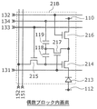
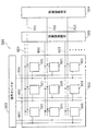
本実施の形態における表示装置は、マトリクス状に配置された複数の発光画素を有する表示装置であって、発光画素列ごとに配置された第1信号線及び第2信号線と、発光画素行ごとに配置された第1制御線、第2制御線及び第3制御線とを備え、複数の発光画素は、複数の発光画素行を一単位とした2以上の駆動ブロックを構成し、複数の発光画素のそれぞれは、駆動トランジスタと、一端子が駆動トランジスタのゲートに接続された第1容量素子と、駆動トランジスタのドレインに接続された発光素子と、ゲートが第1制御線に接続され駆動トランジスタのソースと第1容量素子の他端子の間に挿入された第1スイッチングトランジスタと、ゲートが第2制御線に接続され駆動トランジスタのドレイン電流のオンオフを切り換える第2スイッチングトランジスタと、第1容量素子の他端子と第3制御線との間に挿入された第2容量素子とを備え、奇数番目の駆動ブロックに属する発光画素は、さらに、第1信号線と駆動トランジスタのゲートとの間に挿入された第3スイッチングトランジスタを備え、偶数番目の駆動ブロックに属する発光画素は、さらに、第2信号線と駆動トランジスタのゲートとの間に挿入された第4スイッチングトランジスタを備え、第1制御線、第2制御線及び第3制御線は、同一駆動ブロックの全発光画素では共通化されている。これにより、駆動トランジスタの閾値補正期間及び発光期間を駆動ブロック内で一致させることが可能となる。よって、駆動回路の負担負荷が低減する。また、閾値補正期間を1フレーム期間に対して大きくとることができるので、画像表示品質が向上する。

t1H={1秒/(120Hz×1110本)}×2=7.5μS×2=15μS
となる。ここで、tR(D)=tF(D)=2μS、tR(S)=tF(S)=1.5μSとし、これらを式13に代入すると、Vthの検出期間であるPWSは、2.5μSとなる。
以下、本発明の実施の形態2について、図面を参照しながら説明する。
以下、本発明の実施の形態3について、図面を参照しながら説明する。
10 表示パネル
11A、11B、21A、21B、501 発光画素
12 信号線群
13 制御線群
14 走査/制御線駆動回路
15 信号線駆動回路
20 タイミング制御回路
30 電圧制御回路
110、112 電源線
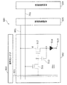
113、213 有機EL素子
114、214、512 駆動トランジスタ
115、116、117、215、216、217、511 スイッチングトランジスタ
118、119 静電保持容量
131 第1制御線
132 第2制御線
133、701、702、703 走査線
134 第3制御線
151 第1信号線
152 第2信号線
500 画像表示装置
502 画素アレイ部
503 信号セレクタ
504 走査線駆動部
505 給電線駆動部
513 保持容量
514 発光素子
515 接地配線
601 信号線
801、802、803 給電線
Claims (9)
- マトリクス状に配置された複数の発光画素を有する表示装置であって、
発光画素列ごとに配置され、発光画素の輝度を決定する信号電圧を前記発光画素に与える第1信号線及び第2信号線と、
第1電源線及び第2電源線と、
発光画素行ごとに配置された走査線と、
発光画素行ごとに配置された第1制御線、第2制御線及び第3制御線を備え、
前記複数の発光画素は、複数の発光画素行を一駆動ブロックとした2以上の駆動ブロックを構成し、
前記複数の発光画素のそれぞれは、
一方の端子が前記第2電源線に接続され、前記信号電圧に応じた信号電流が流れることにより発光する発光素子と、
ソース及びドレインの一方が前記発光素子の他方の端子に接続され、ゲート−ソース間に印加される前記信号電圧を前記信号電流に変換する駆動トランジスタと、
一方の端子が前記駆動トランジスタのゲートに接続された第1容量素子と、
一方の端子が前記第1容量素子の他方の端子に接続され、他方の端子が前記第3制御線に接続された第2容量素子と、
ゲートが前記第1制御線に接続され、ソース及びドレインの一方が前記第1容量素子の他方の端子に接続され、ソース及びドレインの他方が前記駆動トランジスタのソースに接続された第1スイッチングトランジスタと、
ゲートが前記第2制御線に接続され、ソース及びドレインが前記第1電源線と前記駆動トランジスタのソース及びドレインの他方の端子との間に挿入された第2スイッチングトランジスタとを備え、
k(kは自然数)番目の駆動ブロックに属する前記発光画素は、さらに、
ゲートが前記走査線に接続され、ソース及びドレインの一方が前記駆動トランジスタのゲートに接続され、ソース及びドレインの他方が前記第1信号線に接続された第3スイッチングトランジスタを備え、
(k+1)番目の駆動ブロックに属する前記発光画素は、さらに、
ゲートが前記走査線に接続され、ソース及びドレインの一方が前記駆動トランジスタのゲートに接続され、ソース及びドレインの他方が前記第2信号線に接続された第4スイッチングトランジスタを備え、
前記第1制御線及び前記第3制御線は、同一駆動ブロック内の全発光画素では共通化されており、異なる駆動ブロック間では独立している
表示装置。 - さらに、前記第2制御線は、同一駆動ブロック内の全発光画素では共通化されており、異なる駆動ブロック間では独立している
請求項1に記載の表示装置。 - さらに、前記第1信号線、前記第2信号線、前記第1制御線、前記第2制御線、前記第3制御線及び前記走査線を制御して前記発光画素を駆動する駆動回路を具備し、
前記駆動回路は、
前記第2制御線からの制御信号により前記第2スイッチングトランジスタをオフ状態とすることで、k番目の駆動ブロックの有する全ての前記駆動トランジスタへの電源電圧の印加を停止し、
前記走査線からの走査信号により前記第3スイッチングトランジスタをオン状態とすることで、前記第1信号線から基準電圧をk番目の駆動ブロックの有する全ての前記駆動トランジスタのゲートに同時に印加し、
前記第1スイッチングトランジスタがオン状態で前記第3制御線の電圧レベルを変化させることで、前記駆動トランジスタのゲート−ソース間電圧が閾値電圧以上となる初期化電圧をk番目の駆動ブロックの有する全ての前記駆動トランジスタのソースに同時に印加し、
前記走査線からの走査信号により前記第3スイッチングトランジスタをオフ状態とすることで、前記第1信号線とk番目の駆動ブロックの有する全ての前記駆動トランジスタのゲートとを同時に非導通にし、
前記第2制御線からの制御信号により前記第2スイッチングトランジスタをオフ状態とすることで、(k+1)番目の駆動ブロックの有する全ての前記駆動トランジスタへの電源電圧の印加を停止し、
前記走査線からの走査信号により前記第4スイッチングトランジスタをオン状態とすることで、前記第2信号線から前記基準電圧を(k+1)番目の駆動ブロックの有する全ての前記駆動トランジスタのゲートに同時に印加し、
前記第1スイッチングトランジスタがオン状態で前記第3制御線の電圧レベルを変化させることで、前記初期化電圧を(k+1)番目の駆動ブロックの有する全ての前記駆動トランジスタのソースに同時に印加し、
前記走査線からの走査信号により前記第4スイッチングトランジスタをオフ状態とすることで、前記第2信号線と(k+1)番目の駆動ブロックの有する全ての前記駆動トランジスタのゲートとを同時に非導通にする
請求項1または2に記載の表示装置。 - 前記信号電圧は、前記発光素子を発光させるための輝度信号電圧、及び、前記駆動トランジスタの閾値電圧に対応した電圧を前記第1容量素子に記憶させるための基準電圧からなり、
前記表示装置は、さらに、
前記信号電圧を前記第1信号線及び前記第2信号線に出力する信号線駆動回路と、
前記信号線駆動回路が前記信号電圧を出力するタイミングを制御するタイミング制御回路とを備え、
前記タイミング制御回路は、前記信号線駆動回路に前記第1信号線へ前記輝度信号電圧を出力させている間には前記第2信号線へ前記基準電圧を出力させ、前記信号線駆動回路に前記第2信号線へ前記輝度信号電圧を出力させている間には前記第1信号線へ前記基準電圧を出力させる
請求項1〜3のうちいずれか1項に記載の表示装置。 - 全ての前記発光画素を書き換える時間をTfとし、前記駆動ブロックの総数をNとすると、
前記駆動トランジスタの閾値電圧を検出する時間は、
最大でTf/Nである
請求項1〜4のうちいずれか1項に記載の表示装置。 - 複数の信号線のうち一の信号線から供給された輝度信号電圧または基準電圧を当該電圧に対応した信号電流に変換する駆動トランジスタと、前記信号電流が流れることにより発光する発光素子とを備える発光画素がマトリクス状に配置され、複数の前記発光画素行を一駆動ブロックとした2以上の駆動ブロックを構成する表示装置の駆動方法であって、
k(kは自然数)番目の駆動ブロックの有する全ての前記駆動トランジスタのゲートに接続された第1容量素子に、前記駆動トランジスタの閾値電圧に対応した電圧を同時に保持させる第1閾値保持ステップと、
前記第1閾値保持ステップの後、k番目の駆動ブロックの有する前記発光画素において、前記第1容量素子に、前記閾値電圧に対応した電圧に前記輝度信号電圧が加算された加算電圧を発光画素行順に保持させる第1輝度保持ステップと、
前記第1閾値保持ステップの後、(k+1)番目の駆動ブロックの有する全ての前記第1容量素子に、前記駆動トランジスタの閾値電圧に対応した電圧を同時に保持させる第2閾値保持ステップとを含み、
前記第1閾値保持ステップは、
発光画素列ごとに配置された第1信号線から前記基準電圧をk番目の駆動ブロックの有する全ての前記駆動トランジスタのゲートに同時に印加する第1基準電圧印加ステップと、
前記第1基準電圧印加ステップの後、発光画素行ごとに配置された第3制御線から、前記駆動トランジスタのゲート−ソース間電圧が閾値電圧以上となる初期化電圧をk番目の駆動ブロックの有する全ての前記駆動トランジスタのソースに同時に印加する第1初期化電圧印加ステップと、
前記第1初期化電圧印加ステップの後、前記第1信号線とk番目の駆動ブロックの有する全ての前記駆動トランジスタのゲートとを同時に非導通にする第1非導通ステップとを含み、
前記第2閾値保持ステップは、
発光画素列ごとに配置された、前記第1信号線と異なる第2信号線から前記基準電圧を(k+1)番目の駆動ブロックの有する全ての前記駆動トランジスタのゲートに同時に印加する第2基準電圧印加ステップと、
前記第2基準電圧印加ステップの後、発光画素行ごとに配置された第3制御線から、前記初期化電圧を(k+1)番目の駆動ブロックの有する全ての前記駆動トランジスタのソースに同時に印加する第2初期化電圧印加ステップと、
前記第2初期化電圧印加ステップの後、前記第2信号線と(k+1)番目の駆動ブロックの有する全ての前記駆動トランジスタのゲートとを同時に非導通にする第2非導通ステップとを含む
表示装置の駆動方法。 - 前記発光素子は、一方の端子が第2電源線に接続され、他方の端子が前記駆動トランジスタのソース及びドレインの一方に接続され、
前記第1基準電圧印加ステップでは、
ゲートが発光画素行ごとに配置された走査線に接続され、ソース及びドレインの一方が前記駆動トランジスタのゲートに接続され、ソース及びドレインの他方が前記第1信号線に接続された第3スイッチングトランジスタを導通させることにより、前記第1信号線から前記基準電圧を前記駆動トランジスタのゲートに印加し、
前記第2基準電圧印加ステップでは、
ゲートが発光画素行ごとに配置された走査線に接続され、ソース及びドレインの一方が前記駆動トランジスタのゲートに接続され、ソース及びドレインの他方が前記第2信号線に接続された第4スイッチングトランジスタを導通させることにより、前記第2信号線から前記基準電圧を前記駆動トランジスタのゲートに印加し、
第1初期化電圧印加ステップ及び第2初期化電圧印加ステップでは、
ゲートが、発光画素行ごとに配置された第2制御線に接続され、ソース及びドレインが第1電源線と前記駆動トランジスタのソース及びドレインの他方の端子との間に挿入された第2スイッチングトランジスタを非導通にすることにより前記駆動トランジスタへの電源電圧の印加を停止すると共に、ゲートが、発光画素行ごとに配置された第1制御線に接続され、ソース及びドレインの一方が前記第1容量素子の他方の端子に接続され、ソース及びドレインの他方が前記駆動トランジスタのソースに接続された第1スイッチングトランジスタを導通させた状態で、発光画素行ごとに配置された第3制御線から、前記第1スイッチングトランジスタを介して前記初期化電圧を前記駆動トランジスタのソースに印加し、
前記第1非導通ステップでは、
前記第3スイッチングトランジスタを非導通にすることにより、前記第1信号線と前記駆動トランジスタのゲートとを非導通にし、
前記第2非導通ステップでは、
前記第4スイッチングトランジスタを非導通にすることにより、前記第2信号線と前記駆動トランジスタのゲートとを非導通にし、
前記第1輝度保持ステップでは、
前記第3スイッチングトランジスタを導通させることにより、前記第1信号線から前記輝度信号電圧を前記駆動トランジスタのゲートに印加する
請求項6に記載の表示装置の駆動方法。 - さらに、
前記第1輝度保持ステップの後、前記駆動トランジスタのドレイン電流として、k番目の駆動ブロックの有する全ての前記発光素子に、同時に前記信号電流を流して発光させる第1発光ステップを含む
請求項6または7に記載の表示装置の駆動方法。 - さらに、
前記第2閾値保持ステップの後、(k+1)番目の駆動ブロックの有する前記発光画素において、前記第1容量素子に、前記閾値電圧に対応した電圧に前記輝度信号電圧が加算された加算電圧を発光画素行順に保持させる第2輝度保持ステップと、
前記第2輝度保持ステップの後、前記駆動トランジスタのドレイン電流として、(k+1)番目の駆動ブロックの有する全ての前記発光素子に、同時に前記信号電流を流して発光させる第2発光ステップとを含む
請求項8に記載の表示装置の駆動方法。
Applications Claiming Priority (1)
| Application Number | Priority Date | Filing Date | Title |
|---|---|---|---|
| PCT/JP2010/005454 WO2012032560A1 (ja) | 2010-09-06 | 2010-09-06 | 表示装置およびその駆動方法 |
Publications (2)
| Publication Number | Publication Date |
|---|---|
| JPWO2012032560A1 JPWO2012032560A1 (ja) | 2013-10-31 |
| JP5415565B2 true JP5415565B2 (ja) | 2014-02-12 |
Family
ID=45810190
Family Applications (1)
| Application Number | Title | Priority Date | Filing Date |
|---|---|---|---|
| JP2011549089A Expired - Fee Related JP5415565B2 (ja) | 2010-09-06 | 2010-09-06 | 表示装置およびその駆動方法 |
Country Status (5)
| Country | Link |
|---|---|
| US (1) | US8305307B2 (ja) |
| JP (1) | JP5415565B2 (ja) |
| KR (1) | KR101291433B1 (ja) |
| CN (1) | CN102549646B (ja) |
| WO (1) | WO2012032560A1 (ja) |
Families Citing this family (15)
| Publication number | Priority date | Publication date | Assignee | Title |
|---|---|---|---|---|
| CN102576512B (zh) * | 2010-09-06 | 2014-11-12 | 松下电器产业株式会社 | 显示装置及其控制方法 |
| WO2012032567A1 (ja) * | 2010-09-06 | 2012-03-15 | パナソニック株式会社 | 表示装置及びその制御方法 |
| KR101809300B1 (ko) | 2010-09-06 | 2018-01-18 | 가부시키가이샤 제이올레드 | 표시 장치 및 그 구동 방법 |
| KR101928379B1 (ko) * | 2012-06-14 | 2018-12-12 | 엘지디스플레이 주식회사 | 유기발광 다이오드 표시장치 및 그 구동방법 |
| JP2015014764A (ja) * | 2013-07-08 | 2015-01-22 | ソニー株式会社 | 表示装置、表示装置の駆動方法、及び、電子機器 |
| JP6201465B2 (ja) | 2013-07-08 | 2017-09-27 | ソニー株式会社 | 表示装置、表示装置の駆動方法、及び、電子機器 |
| KR102068263B1 (ko) * | 2013-07-10 | 2020-01-21 | 삼성디스플레이 주식회사 | 유기 발광 표시 장치 및 그 구동 방법 |
| JP2015043008A (ja) * | 2013-08-26 | 2015-03-05 | 株式会社ジャパンディスプレイ | 有機el表示装置 |
| KR20160000087A (ko) * | 2014-06-23 | 2016-01-04 | 삼성디스플레이 주식회사 | 화소 및 이를 이용한 유기전계발광 표시장치 |
| KR102122542B1 (ko) | 2014-07-10 | 2020-06-29 | 엘지디스플레이 주식회사 | 유기전계발광표시장치 |
| JP2017083609A (ja) * | 2015-10-27 | 2017-05-18 | ソニー株式会社 | 表示装置、表示装置の駆動方法、表示素子、及び、電子機器 |
| CN105788529A (zh) * | 2016-05-10 | 2016-07-20 | 上海天马有机发光显示技术有限公司 | 一种有机发光显示面板及其驱动方法 |
| KR102470499B1 (ko) * | 2017-05-11 | 2022-11-28 | 삼성디스플레이 주식회사 | 표시 장치 |
| JP6690614B2 (ja) * | 2017-08-30 | 2020-04-28 | ソニー株式会社 | 表示装置 |
| CN110992897B (zh) * | 2019-12-31 | 2021-03-16 | 深圳市华星光电半导体显示技术有限公司 | 显示面板驱动方法、显示驱动电路和显示面板 |
Citations (10)
| Publication number | Priority date | Publication date | Assignee | Title |
|---|---|---|---|---|
| JP2003186439A (ja) * | 2001-12-21 | 2003-07-04 | Matsushita Electric Ind Co Ltd | El表示装置とその駆動方法および情報表示装置 |
| JP2003195809A (ja) * | 2001-12-28 | 2003-07-09 | Matsushita Electric Ind Co Ltd | El表示装置とその駆動方法および情報表示装置 |
| JP2008122633A (ja) * | 2006-11-13 | 2008-05-29 | Sony Corp | 表示装置 |
| WO2008152817A1 (ja) * | 2007-06-15 | 2008-12-18 | Panasonic Corporation | 画像表示装置 |
| WO2009011092A1 (ja) * | 2007-07-19 | 2009-01-22 | Panasonic Corporation | 画像表示装置 |
| JP2009139928A (ja) * | 2007-11-14 | 2009-06-25 | Sony Corp | 表示装置及びその駆動方法と電子機器 |
| JP2009216869A (ja) * | 2008-03-10 | 2009-09-24 | Sony Corp | 表示装置 |
| JP2009237041A (ja) * | 2008-03-26 | 2009-10-15 | Sony Corp | 画像表示装置及び画像表示方法 |
| JP2010054564A (ja) * | 2008-08-26 | 2010-03-11 | Sony Corp | 画像表示装置及び画像表示装置の駆動方法 |
| WO2010041426A1 (ja) * | 2008-10-07 | 2010-04-15 | パナソニック株式会社 | 画像表示装置およびその制御方法 |
Family Cites Families (5)
| Publication number | Priority date | Publication date | Assignee | Title |
|---|---|---|---|---|
| JP2008287141A (ja) | 2007-05-21 | 2008-11-27 | Sony Corp | 表示装置及びその駆動方法と電子機器 |
| KR101517110B1 (ko) | 2007-11-14 | 2015-05-04 | 소니 주식회사 | 표시장치 및 그 구동 방법과 전자기기 |
| JP5254998B2 (ja) | 2008-01-07 | 2013-08-07 | パナソニック株式会社 | 表示装置及び駆動方法 |
| WO2010100938A1 (ja) * | 2009-03-06 | 2010-09-10 | パナソニック株式会社 | 画像表示装置およびその駆動方法 |
| KR101269370B1 (ko) | 2009-05-26 | 2013-05-29 | 파나소닉 주식회사 | 화상 표시 장치 및 그 구동 방법 |
-
2010
- 2010-09-06 WO PCT/JP2010/005454 patent/WO2012032560A1/ja active Application Filing
- 2010-09-06 KR KR1020127006397A patent/KR101291433B1/ko active IP Right Grant
- 2010-09-06 CN CN201080043678.8A patent/CN102549646B/zh not_active Expired - Fee Related
- 2010-09-06 JP JP2011549089A patent/JP5415565B2/ja not_active Expired - Fee Related
-
2012
- 2012-03-16 US US13/421,948 patent/US8305307B2/en active Active
Patent Citations (10)
| Publication number | Priority date | Publication date | Assignee | Title |
|---|---|---|---|---|
| JP2003186439A (ja) * | 2001-12-21 | 2003-07-04 | Matsushita Electric Ind Co Ltd | El表示装置とその駆動方法および情報表示装置 |
| JP2003195809A (ja) * | 2001-12-28 | 2003-07-09 | Matsushita Electric Ind Co Ltd | El表示装置とその駆動方法および情報表示装置 |
| JP2008122633A (ja) * | 2006-11-13 | 2008-05-29 | Sony Corp | 表示装置 |
| WO2008152817A1 (ja) * | 2007-06-15 | 2008-12-18 | Panasonic Corporation | 画像表示装置 |
| WO2009011092A1 (ja) * | 2007-07-19 | 2009-01-22 | Panasonic Corporation | 画像表示装置 |
| JP2009139928A (ja) * | 2007-11-14 | 2009-06-25 | Sony Corp | 表示装置及びその駆動方法と電子機器 |
| JP2009216869A (ja) * | 2008-03-10 | 2009-09-24 | Sony Corp | 表示装置 |
| JP2009237041A (ja) * | 2008-03-26 | 2009-10-15 | Sony Corp | 画像表示装置及び画像表示方法 |
| JP2010054564A (ja) * | 2008-08-26 | 2010-03-11 | Sony Corp | 画像表示装置及び画像表示装置の駆動方法 |
| WO2010041426A1 (ja) * | 2008-10-07 | 2010-04-15 | パナソニック株式会社 | 画像表示装置およびその制御方法 |
Also Published As
| Publication number | Publication date |
|---|---|
| JPWO2012032560A1 (ja) | 2013-10-31 |
| US8305307B2 (en) | 2012-11-06 |
| US20120169799A1 (en) | 2012-07-05 |
| WO2012032560A1 (ja) | 2012-03-15 |
| KR101291433B1 (ko) | 2013-07-30 |
| CN102549646B (zh) | 2014-07-16 |
| KR20120049910A (ko) | 2012-05-17 |
| CN102549646A (zh) | 2012-07-04 |
Similar Documents
| Publication | Publication Date | Title |
|---|---|---|
| JP5415565B2 (ja) | 表示装置およびその駆動方法 | |
| JP4778115B2 (ja) | 画像表示装置 | |
| JP5456901B2 (ja) | 表示装置およびその駆動方法 | |
| JP5282146B2 (ja) | 表示装置及びその制御方法 | |
| JP5230806B2 (ja) | 画像表示装置およびその駆動方法 | |
| JP5627694B2 (ja) | 表示装置 | |
| JP5284492B2 (ja) | 表示装置及びその制御方法 | |
| JP5414808B2 (ja) | 表示装置およびその駆動方法 | |
| JP5399521B2 (ja) | 表示装置およびその駆動方法 | |
| KR20040099162A (ko) | 액티브 매트릭스형 표시 장치 |
Legal Events
| Date | Code | Title | Description |
|---|---|---|---|
| A131 | Notification of reasons for refusal |
Free format text: JAPANESE INTERMEDIATE CODE: A131 Effective date: 20130827 |
|
| A521 | Request for written amendment filed |
Free format text: JAPANESE INTERMEDIATE CODE: A523 Effective date: 20130926 |
|
| TRDD | Decision of grant or rejection written | ||
| A01 | Written decision to grant a patent or to grant a registration (utility model) |
Free format text: JAPANESE INTERMEDIATE CODE: A01 Effective date: 20131022 |
|
| A61 | First payment of annual fees (during grant procedure) |
Free format text: JAPANESE INTERMEDIATE CODE: A61 Effective date: 20131113 |
|
| R150 | Certificate of patent or registration of utility model |
Ref document number: 5415565 Country of ref document: JP Free format text: JAPANESE INTERMEDIATE CODE: R150 |
|
| S111 | Request for change of ownership or part of ownership |
Free format text: JAPANESE INTERMEDIATE CODE: R313111 |
|
| R350 | Written notification of registration of transfer |
Free format text: JAPANESE INTERMEDIATE CODE: R350 |
|
| R250 | Receipt of annual fees |
Free format text: JAPANESE INTERMEDIATE CODE: R250 |
|
| R250 | Receipt of annual fees |
Free format text: JAPANESE INTERMEDIATE CODE: R250 |
|
| R250 | Receipt of annual fees |
Free format text: JAPANESE INTERMEDIATE CODE: R250 |
|
| R250 | Receipt of annual fees |
Free format text: JAPANESE INTERMEDIATE CODE: R250 |
|
| R250 | Receipt of annual fees |
Free format text: JAPANESE INTERMEDIATE CODE: R250 |
|
| R250 | Receipt of annual fees |
Free format text: JAPANESE INTERMEDIATE CODE: R250 |
|
| R250 | Receipt of annual fees |
Free format text: JAPANESE INTERMEDIATE CODE: R250 |
|
| LAPS | Cancellation because of no payment of annual fees |