WO2022071283A1 - 光導波路素子及びそれを用いた光変調デバイス並びに光送信装置 - Google Patents
光導波路素子及びそれを用いた光変調デバイス並びに光送信装置 Download PDFInfo
- Publication number
- WO2022071283A1 WO2022071283A1 PCT/JP2021/035550 JP2021035550W WO2022071283A1 WO 2022071283 A1 WO2022071283 A1 WO 2022071283A1 JP 2021035550 W JP2021035550 W JP 2021035550W WO 2022071283 A1 WO2022071283 A1 WO 2022071283A1
- Authority
- WO
- WIPO (PCT)
- Prior art keywords
- optical waveguide
- optical
- substrate
- modulation
- waveguide element
- Prior art date
Links
Images


Classifications
-
- G—PHYSICS
- G02—OPTICS
- G02F—OPTICAL DEVICES OR ARRANGEMENTS FOR THE CONTROL OF LIGHT BY MODIFICATION OF THE OPTICAL PROPERTIES OF THE MEDIA OF THE ELEMENTS INVOLVED THEREIN; NON-LINEAR OPTICS; FREQUENCY-CHANGING OF LIGHT; OPTICAL LOGIC ELEMENTS; OPTICAL ANALOGUE/DIGITAL CONVERTERS
- G02F1/00—Devices or arrangements for the control of the intensity, colour, phase, polarisation or direction of light arriving from an independent light source, e.g. switching, gating or modulating; Non-linear optics
- G02F1/01—Devices or arrangements for the control of the intensity, colour, phase, polarisation or direction of light arriving from an independent light source, e.g. switching, gating or modulating; Non-linear optics for the control of the intensity, phase, polarisation or colour
- G02F1/03—Devices or arrangements for the control of the intensity, colour, phase, polarisation or direction of light arriving from an independent light source, e.g. switching, gating or modulating; Non-linear optics for the control of the intensity, phase, polarisation or colour based on ceramics or electro-optical crystals, e.g. exhibiting Pockels effect or Kerr effect
- G02F1/035—Devices or arrangements for the control of the intensity, colour, phase, polarisation or direction of light arriving from an independent light source, e.g. switching, gating or modulating; Non-linear optics for the control of the intensity, phase, polarisation or colour based on ceramics or electro-optical crystals, e.g. exhibiting Pockels effect or Kerr effect in an optical waveguide structure
-
- G—PHYSICS
- G02—OPTICS
- G02B—OPTICAL ELEMENTS, SYSTEMS OR APPARATUS
- G02B6/00—Light guides; Structural details of arrangements comprising light guides and other optical elements, e.g. couplings
- G02B6/10—Light guides; Structural details of arrangements comprising light guides and other optical elements, e.g. couplings of the optical waveguide type
- G02B6/12—Light guides; Structural details of arrangements comprising light guides and other optical elements, e.g. couplings of the optical waveguide type of the integrated circuit kind
- G02B6/122—Basic optical elements, e.g. light-guiding paths
- G02B6/125—Bends, branchings or intersections
-
- G—PHYSICS
- G02—OPTICS
- G02F—OPTICAL DEVICES OR ARRANGEMENTS FOR THE CONTROL OF LIGHT BY MODIFICATION OF THE OPTICAL PROPERTIES OF THE MEDIA OF THE ELEMENTS INVOLVED THEREIN; NON-LINEAR OPTICS; FREQUENCY-CHANGING OF LIGHT; OPTICAL LOGIC ELEMENTS; OPTICAL ANALOGUE/DIGITAL CONVERTERS
- G02F1/00—Devices or arrangements for the control of the intensity, colour, phase, polarisation or direction of light arriving from an independent light source, e.g. switching, gating or modulating; Non-linear optics
- G02F1/01—Devices or arrangements for the control of the intensity, colour, phase, polarisation or direction of light arriving from an independent light source, e.g. switching, gating or modulating; Non-linear optics for the control of the intensity, phase, polarisation or colour
- G02F1/0147—Devices or arrangements for the control of the intensity, colour, phase, polarisation or direction of light arriving from an independent light source, e.g. switching, gating or modulating; Non-linear optics for the control of the intensity, phase, polarisation or colour based on thermo-optic effects
-
- G—PHYSICS
- G02—OPTICS
- G02F—OPTICAL DEVICES OR ARRANGEMENTS FOR THE CONTROL OF LIGHT BY MODIFICATION OF THE OPTICAL PROPERTIES OF THE MEDIA OF THE ELEMENTS INVOLVED THEREIN; NON-LINEAR OPTICS; FREQUENCY-CHANGING OF LIGHT; OPTICAL LOGIC ELEMENTS; OPTICAL ANALOGUE/DIGITAL CONVERTERS
- G02F1/00—Devices or arrangements for the control of the intensity, colour, phase, polarisation or direction of light arriving from an independent light source, e.g. switching, gating or modulating; Non-linear optics
- G02F1/01—Devices or arrangements for the control of the intensity, colour, phase, polarisation or direction of light arriving from an independent light source, e.g. switching, gating or modulating; Non-linear optics for the control of the intensity, phase, polarisation or colour
- G02F1/21—Devices or arrangements for the control of the intensity, colour, phase, polarisation or direction of light arriving from an independent light source, e.g. switching, gating or modulating; Non-linear optics for the control of the intensity, phase, polarisation or colour by interference
- G02F1/212—Mach-Zehnder type
-
- G—PHYSICS
- G02—OPTICS
- G02F—OPTICAL DEVICES OR ARRANGEMENTS FOR THE CONTROL OF LIGHT BY MODIFICATION OF THE OPTICAL PROPERTIES OF THE MEDIA OF THE ELEMENTS INVOLVED THEREIN; NON-LINEAR OPTICS; FREQUENCY-CHANGING OF LIGHT; OPTICAL LOGIC ELEMENTS; OPTICAL ANALOGUE/DIGITAL CONVERTERS
- G02F1/00—Devices or arrangements for the control of the intensity, colour, phase, polarisation or direction of light arriving from an independent light source, e.g. switching, gating or modulating; Non-linear optics
- G02F1/01—Devices or arrangements for the control of the intensity, colour, phase, polarisation or direction of light arriving from an independent light source, e.g. switching, gating or modulating; Non-linear optics for the control of the intensity, phase, polarisation or colour
- G02F1/21—Devices or arrangements for the control of the intensity, colour, phase, polarisation or direction of light arriving from an independent light source, e.g. switching, gating or modulating; Non-linear optics for the control of the intensity, phase, polarisation or colour by interference
- G02F1/225—Devices or arrangements for the control of the intensity, colour, phase, polarisation or direction of light arriving from an independent light source, e.g. switching, gating or modulating; Non-linear optics for the control of the intensity, phase, polarisation or colour by interference in an optical waveguide structure
-
- G—PHYSICS
- G02—OPTICS
- G02F—OPTICAL DEVICES OR ARRANGEMENTS FOR THE CONTROL OF LIGHT BY MODIFICATION OF THE OPTICAL PROPERTIES OF THE MEDIA OF THE ELEMENTS INVOLVED THEREIN; NON-LINEAR OPTICS; FREQUENCY-CHANGING OF LIGHT; OPTICAL LOGIC ELEMENTS; OPTICAL ANALOGUE/DIGITAL CONVERTERS
- G02F2201/00—Constructional arrangements not provided for in groups G02F1/00 - G02F7/00
- G02F2201/12—Constructional arrangements not provided for in groups G02F1/00 - G02F7/00 electrode
- G02F2201/127—Constructional arrangements not provided for in groups G02F1/00 - G02F7/00 electrode travelling wave
-
- G—PHYSICS
- G02—OPTICS
- G02F—OPTICAL DEVICES OR ARRANGEMENTS FOR THE CONTROL OF LIGHT BY MODIFICATION OF THE OPTICAL PROPERTIES OF THE MEDIA OF THE ELEMENTS INVOLVED THEREIN; NON-LINEAR OPTICS; FREQUENCY-CHANGING OF LIGHT; OPTICAL LOGIC ELEMENTS; OPTICAL ANALOGUE/DIGITAL CONVERTERS
- G02F2202/00—Materials and properties
- G02F2202/20—LiNbO3, LiTaO3
Definitions
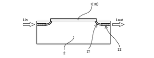
- FIGS. 1 and 2 the substrate 1 such as lithium niobate (LN) is thinned to a thickness of 20 ⁇ m or less, and the optical waveguide 10 is formed on the substrate 1.
- FIG. 1 is a plan view of an optical waveguide element constituting an optical modulator, and electrodes such as a modulation electrode are omitted for simplification.
- FIG. 2 is a side view of FIG. 1.
- the substrate 1 to be a thin plate is joined to the holding substrate 2 via the adhesive layer 3. Lin indicates incident light, and Lout indicates emitted light.
- the new thin plate structure optical modulator In order to use it as an integrated LN optical modulator such as HB-CDM (High Bandwidth-Coherent Driver Modulator), it is essential to reduce the size of the optical waveguide element, and to reduce the drive voltage, the cross-sectional structure of the optical waveguide is further reduced. There must be. Therefore, as shown in FIG. 3, in the new thin plate structure optical modulator, it is necessary to thin the substrate 1 such as lithium niobate (LN) to a thickness of 2 ⁇ m or less, and the adhesive layer having a significantly different coefficient of thermal expansion is required. It is required to directly bond to the holding substrate 2 without using the above.
- LN lithium niobate
- the optical mode field diameter of the optical waveguide 10 is about 1 ⁇ m, which is larger than the optical mode field diameter of 10 ⁇ m of the optical fiber. Therefore, the light loss at the connection between the optical waveguide element and the optical fiber at the incident part or the exit part is about 0.5 dB at one end of the conventional thin plate structure (thickness about 10 ⁇ m) optical modulator, but it is new.
- the optical modulator of the thin plate structure of is significantly increased to 14 dB or more at one end.
- Non-Patent Document 1 In the case of an optical modulator using a semiconductor material in order to reduce the optical loss due to the coupling with the optical fiber, as shown in FIG. 4 or FIG. A method of converting the optical mode field diameter (MFD) by providing a vertical tapered optical waveguide (see reference numeral 12 in FIG. 5) has been proposed. (See Non-Patent Document 1)
- the problem to be solved by the present invention is to solve the above-mentioned problems and to provide an optical waveguide element which is compact, has low light loss, and has long-term stability. Further, it is to provide an optical modulation device and an optical transmission device using the optical waveguide element.
- the optical waveguide element of the present invention, the optical modulation device using the optical waveguide element, and the optical transmission device have the following technical features.
- the optical waveguide A is formed on the first substrate, and at the end of the first substrate, an incident portion for incident the light wave on the optical waveguide A or an exit portion for emitting the light wave from the optical waveguide A is provided.
- the optical waveguide B is formed on the second substrate, and the second substrate has an optical waveguide that modulates the light wave propagating in the optical waveguide B, and at least the optical waveguide A is provided.
- a part of the optical waveguide element is characterized by having a conversion unit that converts the optical mode field diameter.
- optical waveguide element according to (1) above is characterized in that the optical mode field diameter of the light wave converted by the conversion unit is in the range of 2 ⁇ m or more and 5 ⁇ m or less.
- the thickness of the second substrate is 2 ⁇ m or less.
- the optical waveguide A and the optical waveguide B in the optical waveguide A are connected and formed on the first substrate.
- the connected optical waveguide to be made is characterized in that it is formed by either ion implantation, ion exchange, or an ultrashort pulse laser.
- either the first substrate or the second substrate is provided with a phase adjusting electrode. It is a feature.
- a bent portion in which the traveling direction of the light wave rotates 180 degrees is formed in either the optical waveguide A or the optical waveguide B. It is characterized by being done.
- the optical waveguide element according to any one of (1) to (6) above is housed in a housing, and the housing is provided with an optical fiber that inputs or outputs light waves to the optical waveguide. It is a modulation device.
- the optical modulation section of the optical waveguide element is provided with a modulation electrode, and an electronic circuit for amplifying a modulation signal input to the modulation electrode is installed inside the housing. It is characterized by having.
- An optical transmission device comprising the optical modulation device according to (7) or (8) above, and an electronic circuit that outputs a modulation signal that causes the optical modulation device to perform a modulation operation.
- FIG. 7 It is sectional drawing in FIG. 7 one-dot chain line AA'. It is a figure which shows the change of the coupling efficiency when the mode field diameter of a conversion part is changed. It is a side view which shows the 2nd Embodiment of the optical waveguide element of this invention. It is a top view which shows the 3rd Embodiment of the optical waveguide element of this invention. It is a top view which shows the 4th Embodiment of the optical waveguide element of this invention. It is a top view which shows the 5th Embodiment of the optical waveguide element of this invention. It is a top view explaining the optical modulation device and the optical transmission apparatus of this invention.
- the material 1 of the second substrate used in the optical waveguide element of the present invention is composed of a material having an electro-optical effect, and in particular, lithium niobate (LN) or lithium tantalate (LT), PLZT (titanium zirconate). Substrates such as lead acid lanthanum) or vapor deposition films made of these materials can be used. Further, various materials such as semiconductor materials and organic materials can also be used as optical waveguides.
- a rib-type optical waveguide having a convex portion corresponding to the optical waveguide is formed on the substrate, such as etching a substrate 1 other than the optical waveguide or forming grooves on both sides of the optical waveguide. It is possible to use it. Further, it is also possible to further increase the refractive index of the optical waveguide by diffusing Ti or the like on the substrate surface by a heat diffusion method, a proton exchange method, or the like in accordance with the rib-type optical waveguide.
- the thickness of the second substrate (thin plate) on which the optical waveguide 10 is formed is set to 2 ⁇ m or less in order to match the speed between the microwave and the light wave of the modulated signal.
- the height of the rib-type optical waveguide is set to 1 ⁇ m or less, more preferably 0.4 ⁇ m or less. It is also possible to form a vapor phase growth film on the first substrate 2 which is a holding substrate and process the film into the shape of an optical waveguide.
- the first substrate 2 as a holding substrate is directly bonded to the second substrate 1 on which the optical waveguide is formed, without using a resin layer (adhesive layer).
- the first substrate 2 has a lower refractive index than the second substrate and has a coefficient of thermal expansion close to that of an optical waveguide or the like, for example, a substrate containing an oxide layer such as quartz or glass (referred to as “glass material”). Is preferably used.
- a composite substrate in which a silicon oxide layer is formed on a silicon substrate, which is abbreviated as SOI or LNOI, or a silicon oxide layer is formed on an LN substrate can also be used.
- the feature of the optical waveguide element of the present invention is that, as shown in FIGS. 7 and 8, an embedded optical waveguide A (20) is formed at an end portion of a first substrate (for example, a glass substrate). It is a feature. A part or all of the optical waveguide A functions as a conversion unit that changes the optical mode field diameter of the propagating light wave. Then, as an example, after the second substrate (for example, LN substrate) is directly bonded to the first substrate on which the optical waveguide A is formed, the second substrate is polished to 2 ⁇ m or less to be thinned, and then dry or wet. A rib-type optical waveguide B (10) can be formed on the second substrate by the etching method according to the above method.
- FIG. 9 shows a cross-sectional view taken along the alternate long and short dash line AA'in FIG.
- the width s1 of the optical waveguide is set in the range of 0.2 to 2.0 ⁇ m
- the height t1 is set in the range of 0.2 to 2.0 ⁇ m.
- the distance s2 to the protrusion (the substrate portion remaining without etching) of the substrate adjacent to the optical waveguide is 5.0 to 50.0 ⁇ m
- the thickness of the second substrate 1 is 0.5 to 2.0 ⁇ m. Is set to.
- the optical mode field diameter (10 ⁇ m) of the optical fiber and the optical mode field diameter (1 ⁇ m) of the LN substrate having the optical modulator are rapidly increased. It is possible to prevent an increase in light loss due to such changes.
- the exit side end of the rib-type optical waveguide (10) has a tapered structure, so that the mode can be smoothly transferred to the optical waveguide formed on the first substrate.
- the optical mode field diameter w2 of the second substrate is 0.5 ⁇ m, 1.0 ⁇ m, and 2.0 ⁇ m
- the optical mode field diameter w1 of the first substrate is 1.0 ⁇ m to 10.0 ⁇ m.
- the optical mode field diameter is simply calculated by the difference in the optical mode field diameter as the average of the optical mode field diameters in the vertical direction and the horizontal direction.
- each graph is standardized based on the peak value.
- the optical mode field diameter is set to include a region where w1 is 2 ⁇ m or more and 5 ⁇ m or less, thereby preventing a significant decrease in coupling efficiency. This can lead to a reduction in light loss. Further, since a steep change in the optical mode field diameter leads to an increase in optical loss, it is expected that the optical loss will be further reduced by gently changing w1 of the optical waveguide A and w2 of the optical waveguide B.
- w1 of the optical waveguide A (20) is larger than w2 of the optical waveguide B (10), and the optical waveguide A and the optical waveguide B are at least when the first substrate is viewed in a plan view. It is desirable that they overlap. However, when the evanescent wave of each optical waveguide is used, the optical waveguide A and the optical waveguide B do not have to overlap each other within the range of optical coupling. Further, it is desirable that the refractive index n1 of the optical waveguide A (20) is smaller than the refractive index n2 of the optical waveguide B (10).
- Examples of the method for forming the embedded optical waveguide A on the first substrate (glass substrate) include ion exchange, ion implantation, and ultrashort pulse laser drawing.
- ion exchange when a mask pattern is formed on a glass substrate such as soda glass with a metal film such as titanium and immersed in a potassium nitrate melt at 300 to 400 ° C., only the opening portion of the metal film is selectively ion exchanged.
- the optical waveguide is formed.
- the refractive index can be increased by about 0.01 to 0.1 depending on conditions such as immersion temperature, time, and applied voltage. K, Ag, Tl and the like can be used for ion exchange.
- Such a configuration can have a larger difference in refractive index than an optical waveguide in which titanium is thermally diffused in lithium niobate.
- the optical mode field diameter of the glass substrate can be made smaller than the optical mode field diameter (10 ⁇ m) of the optical fiber. Therefore, the optical mode field diameter of the substrate can be set to the above-mentioned region of 2 ⁇ m or more and 5 ⁇ m or less, so that it is possible to prevent a significant decrease in the coupling efficiency with the optical fiber.
- an optical waveguide can be formed on one surface of the first substrate. After polishing the surface of the glass substrate, it is directly bonded to the LN substrate, and then the LN substrate is polished to 2 ⁇ m or less. After forming a rib-type waveguide by dry etching on the LN substrate, a gold electrode is formed by a plating method.
- the condensed irradiation of a femtosecond laser induces a structural change inside the glass, so that the refractive index changes and an optical waveguide is formed. It is possible to increase the refractive index near the focal point of the laser beam by about 0.01 depending on the conditions such as pulse width, repetition frequency, and pulse energy.
- the silicon and oxygen networks that make up ordinary silica glass are dominated by 6- or 5-membered rings, but the network at the site irradiated with the ultrashort pulse laser has a reduced number of members, and the 3-membered ring, The number of 4-membered rings increases.
- the content of the 3- or 4-membered ring of silicon and oxygen in the silica glass in the optical waveguide formed by the focused irradiation of the femtosecond laser is the other of the substrate on which the optical waveguide is formed. It will be larger than the content in the portion.
- the optical waveguide with an increased 3-membered ring and 4-membered ring has an improved density and an increased mechanical strength as compared with other parts where the membered ring does not change.
- the optical waveguide is formed by an ultrashort pulse laser
- the optical waveguide is limited to the focal point of the laser light. Therefore, the optical waveguide of the LN substrate having the optical modulation unit and the optical waveguide formed on the glass substrate are three-dimensionally connected. It is also possible to provide an optical waveguide element with lower loss.
- the optical waveguide (22) and the connected optical waveguide (21) can also be formed by an ultrashort pulse laser or the above-mentioned ion exchange or ion implantation.
- the connected optical waveguide (21) is three-dimensionally formed in the thickness direction of the first substrate (glass substrate) (2) as shown in FIG. 11, the light loss is reduced and the mechanical intensity is reduced.
- at least the connected optical waveguide (21) may be formed by an ultrashort pulse laser to increase the number of 3-membered rings and 4-membered rings.
- the refractive index of the connected optical waveguide (21) may be formed so as to gradually increase from the optical waveguide (10) side to the optical waveguide (22) side.
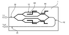
- FIG. 12 is a structure for reducing light loss only in the light input / output portion (the portion of the optical waveguide (20)).
- FIG. 13 has a structure in which a light input / output portion, a 180 ° bent portion (R2), and a straight line portion connecting the bent portion to the exit portion are formed on the first substrate to reduce light loss.
- FIG. 14 shows a structure in which the light input / output portion, the 180 ° bent portion, the straight portion, and the Mach-Zehnder branch portion are formed on the first substrate except for the optical modulation portion to reduce the light loss. It has become.
- Reference numeral MEs shown in FIGS. 12 to 14 are traveling wave type modulation electrodes, and reference numeral BE is a bias electrode for phase adjustment.
- the phase adjusting electrode BE is provided on the second substrate (LN substrate), it is composed of a DC bias electrode.
- the electrode BE when the electrode BE is provided on the first substrate (glass substrate), it becomes a heating electrode using the thermo-optical effect.
- the incident portion (Lin) and the exit portion (Lout) in FIGS. 12 to 14 may be interchanged. In this case, the positions of the modulation electrode and the bias electrode are appropriately changed.
- the transmission distance of the optical waveguide on the incident side is long, it is desirable that the polarization state of light is maintained.
- an optical transmission device OTA by connecting an electronic circuit (digital signal processor DSP) that outputs a modulation signal that causes the optical modulation device MD to perform a modulation operation to the optical modulation device MD. Since the modulation signal applied to the optical waveguide element needs to be amplified, the driver circuit DRV is used.
- the driver circuit DRV and the digital signal processor DSP can be arranged outside the housing 8, but can also be arranged inside the housing 8. In particular, by arranging the driver circuit DRV in the housing, it is possible to further reduce the propagation loss of the modulated signal from the driver circuit.
- an optical waveguide device which is compact, has low light loss, and has long-term stability. Further, it becomes possible to provide an optical modulation device and an optical transmission device using the optical waveguide element.
- Second board 2 First board 10 Optical waveguide B 20 Optical Waveguide A (including a part or all of the optical mode field diameter converter)
Landscapes
- Physics & Mathematics (AREA)
- Nonlinear Science (AREA)
- General Physics & Mathematics (AREA)
- Optics & Photonics (AREA)
- Engineering & Computer Science (AREA)
- Microelectronics & Electronic Packaging (AREA)
- Chemical & Material Sciences (AREA)
- Ceramic Engineering (AREA)
- Crystallography & Structural Chemistry (AREA)
- Optical Integrated Circuits (AREA)
- Optical Modulation, Optical Deflection, Nonlinear Optics, Optical Demodulation, Optical Logic Elements (AREA)
Abstract
小型かつ低光損失で長期安定性を有する光導波路素子を提供すること。 第一の基板(2)に光導波路A(20)が形成され、前記第一の基板の端部には、該光導波路Aへ光波を入射する入射部又は該光導波路Aから光波を出射する出射部を有しており、第二の基板(1)に光導波路B(10)が形成され、前記第二の基板には該光導波路Bを伝搬する光波を変調する光変調部を有しており、該光導波路A(20)の少なくとも一部には、光モードフィールド径を変換する変換部(20)を有することを特徴とする光導波路素子である。
Description
本発明は、光導波路素子及びそれを用いた光変調デバイス並びに光送信装置に関する。
次世代の光ファイバー通信で用いられる光変調器は、多値変調に利用されるため、小型で低光損失かつ長期安定性を有することが必要になる。光変調器などの小型化を実現する上で、低駆動電圧化のために光と電界の重なり効率を向上させた、薄板構造の光変調器が提案されている。(特許文献1参照)
従来の薄板構造の光変調器は、図1及び2に示すように、ニオブ酸リチウム(LN)等の基板1を20μm以下の厚みに薄板化すると共に、該基板1に光導波路10を形成している。図1は、光変調器を構成する光導波素子の平面図であり、変調電極等の電極は、簡略化のため省略している。図2は、図1の側面図である。薄板となる基板1は、接着層3を介して保持基板2に接合されている。Linは入射光、Loutは出射光を示す。
HB-CDM(High Bandwidth-Coherent Driver Modulator)などの集積型LN光変調器として用いるためには、光導波路素子の小型化が必須となり、駆動電圧低減のため、光導波路の断面構造も更に小型化しなければならない。そのため、図3に示すように、新規の薄板構造の光変調器は、ニオブ酸リチウム(LN)等の基板1を2μm以下の厚みに薄板化する必要があり、熱膨張係数の大きく異なる接着層を介さず、保持基板2に直接接合することが求められる。
基板1の厚みを2μm以下とすると、光導波路10の光モードフィールド径は1μm程度であり、光ファイバーの光モードフィールド径の10μmと比較し、両者の差異が大きくなる。このため、入射部又は出射部における光導波路素子と光ファイバーとの接続部における光損失は、従来の薄板構造(厚さ10μm程度)の光変調器は片端で0.5dB程度であったが、新規の薄板構造の光変調器は片端で14dB以上と大幅に増加する。
光ファイバーとの結合による光損失を低減するため、半導体材料を用いた光変調器の場合には、図4又は図5のように、入射部と出射部に水平方向のテーパ光導波路(図4の符号11参照)又は、垂直方向のテーパ光導波路(図5の符号12参照)を設けて光モードフィールド径(MFD)を変換する方法が提案されている。(非特許文献1参照)
しかし、これらの水平方向又は垂直方向のテーパ光導波路でMFDを拡大させることは作製プロセスが複雑であることが大きな問題となっている。一方、図6に示すように、薄板構造の入射部と出射部に有機材料からなる光導波路13を設けて光モードフィールド径を変換する場合、作製プロセスは比較的容易になるが、有機材料の光耐久性などの長期安定性が問題になる。
内田泰芳ほか,"2.5%Δ石英系PLCを用いた低接続損失可能なバーティカルスポットサイズ変換器(SSC)の開発",古河電工時報,第125号,pp.1-5,2010.
本発明が解決しようとする課題は、上述したような問題を解決し、小型かつ低光損失で長期安定性を有する光導波路素子を提供することである。さらには、その光導波路素子を用いた光変調デバイスと光送信装置を提供することである。
上記課題を解決するため、本発明の光導波路素子及びそれを用いた光変調デバイス並びに光送信装置は、以下の技術的特徴を有する。
(1) 第一の基板に光導波路Aが形成され、前記第一の基板の端部には、該光導波路Aへ光波を入射する入射部又は該光導波路Aから光波を出射する出射部を有しており、第二の基板に光導波路Bが形成され、前記第二の基板には該光導波路Bを伝搬する光波を変調する光変調部を有しており、該光導波路Aの少なくとも一部には、光モードフィールド径を変換する変換部を有することを特徴とする光導波路素子である。
(1) 第一の基板に光導波路Aが形成され、前記第一の基板の端部には、該光導波路Aへ光波を入射する入射部又は該光導波路Aから光波を出射する出射部を有しており、第二の基板に光導波路Bが形成され、前記第二の基板には該光導波路Bを伝搬する光波を変調する光変調部を有しており、該光導波路Aの少なくとも一部には、光モードフィールド径を変換する変換部を有することを特徴とする光導波路素子である。
(2) 上記(1)に記載の光導波路素子において、該変換部で変換された光波の光モードフィールド径は、2μm以上、5μm以下の範囲であることを特徴とする。
(3) 上記(1)又は(2)に記載の光導波路素子において、前記第二の基板の厚みが2μm以下であることを特徴とする。
(4) 上記(1)乃至(3)のいずれかに記載の光導波路素子において、該光導波路Aの中の該光導波路Aと該光導波路Bと接続すると共に、該第一の基板に形成される接続光導波路は、イオン注入、イオン交換、又は超短パルスレーザーのいずれかで形成されていることを特徴とする。
(5) 上記(1)乃至(4)のいずれかに記載の光導波路素子において、前記第一の基板又は前記第二の基板のいずれかには、位相調整用電極が設けられていることを特徴とする。
(6) 上記(1)乃至(5)のいずれかに記載の光導波路素子において、該光導波路A又は該光導波路Bのいずれかには、光波の進行方向が180度回転する曲げ部が形成されていることを特徴とする。
(7) 上記(1)乃至(6)いずれかに記載の光導波路素子が筐体内に収容され、該筐体には該光導波路に光波を入力又は出力する光ファイバーを備えることを特徴とする光変調デバイスである。
(8) 上記(7)に記載の光変調デバイスにおいて、該光導波路素子の該光変調部は変調電極を備え、該変調電極に入力する変調信号を増幅する電子回路を該筐体の内部に有することを特徴とする。
(9) 上記(7)又は(8)に記載の光変調デバイスと、該光変調デバイスに変調動作を行わせる変調信号を出力する電子回路とを有することを特徴とする光送信装置である。
本発明は、第一の基板に光導波路Aが形成され、前記第一の基板の端部には、該光導波路Aへ光波を入射する入射部又は該光導波路Aから光波を出射する出射部を有しており、第二の基板に光導波路Bが形成され、前記第二の基板には該光導波路Bを伝搬する光波を変調する光変調部を有しており、該光導波路Aの少なくとも一部には、光モードフィールド径を変換する変換部を有するので、光変調部を有する第二の基板の優れた特性を維持しながら、第二の基板とは異なる第一の基板に変換部を形成でき、小型かつ低光損失で長期安定性を有する光導波路素子を提供することが可能となる。
以下、本発明の光導波路素子について、好適例を用いて詳細に説明する。
本発明の光導波路素子は、図7及び8に示すよう、第一の基板(2)に光導波路A(20)が形成され、前記第一の基板の端部には、該光導波路Aへ光波を入射する入射部又は該光導波路Aから光波を出射する出射部を有しており、第二の基板(1)に光導波路B(10)が形成され、前記第二の基板には該光導波路Bを伝搬する光波を変調する光変調部を有しており、該光導波路A(20)の少なくとも一部には、光モードフィールド径を変換する変換部(20)を有することを特徴とする光導波路素子である。
本発明の光導波路素子は、図7及び8に示すよう、第一の基板(2)に光導波路A(20)が形成され、前記第一の基板の端部には、該光導波路Aへ光波を入射する入射部又は該光導波路Aから光波を出射する出射部を有しており、第二の基板(1)に光導波路B(10)が形成され、前記第二の基板には該光導波路Bを伝搬する光波を変調する光変調部を有しており、該光導波路A(20)の少なくとも一部には、光モードフィールド径を変換する変換部(20)を有することを特徴とする光導波路素子である。
本発明の光導波路素子に使用される第二の基板の材料1は、電気光学効果を有する材料で構成され、特に、ニオブ酸リチウム(LN)又はタンタル酸リチウム(LT)、PLZT(ジルコン酸チタン酸鉛ランタン)などの基板又は、これらの材料による気相成長膜などが利用可能である。
また、半導体材料又は有機材料など種々の材料も光導波路として利用可能である。
また、半導体材料又は有機材料など種々の材料も光導波路として利用可能である。
光導波路10の形成方法としては、光導波路以外の基板1をエッチングしたり、光導波路の両側に溝を形成するなど、基板に光導波路に対応する部分を凸状としたリブ型の光導波路を利用することが可能である。さらに、リブ型の光導波路に合わせて、Tiなどを熱拡散法又はプロトン交換法などで基板表面に拡散させることにより、光導波路の屈折率をより高くすることも可能である。
光導波路10を形成した第二の基板(薄板)の厚さは、変調信号のマイクロ波と光波との速度整合を図るため、2μm以下に設定される。また、リブ型光導波路の高さは、1μm以下、より好ましくは0.4μm以下に設定される。また、保持基板である第一の基板2の上に気相成長膜を形成し、当該膜を光導波路の形状に加工することも可能である。
光導波路を形成した第二の基板1には、機械的強度を高めるため、保持基板として第一の基板2が、樹脂層(接着層)を介さず、直接接合されている。第一の基板2としては、第二の基板よりも屈折率が低く、光導波路などと熱膨張率が近い材料、例えば水晶又はガラス等の酸化物層を含む基板(「ガラス材料」という。)が好適に利用される。SOI、LNOIと略されるシリコン基板上に酸化ケイ素層又はLN基板上に酸化ケイ素層を形成した複合基板も利用可能である。
本発明の光導波路素子の特徴は、図7及び図8に示すように、第一の基板(例えば、ガラス基板)の端部に埋め込み型の光導波路A(20)を形成していることを特徴とする。光導波路Aの一部又は全部は、伝搬する光波の光モードフィールド径を変化させる変換部として機能している。そして、一例としては、光導波路Aを形成した第一の基板に第二の基板(例えば、LN基板)を直接接合した後、第二の基板を2μm以下まで研磨して薄板化し、ドライもしくはウェットによるエッチング法で第二の基板にリブ型の光型導波路B(10)を形成することができる。
図9は、図8の一点鎖線A-A’における断面図を示している。リブ型光導波路(10)を形成する場合に、光導波路の幅s1は0.2~2.0μm、高さt1は0.2~2.0μmの範囲で設定される。また、光導波路と隣接する基板の突起部(エッチングされずに残った基板部分)までの距離s2は5.0~50.0μm、第二の基板1の厚さは0.5~2.0μmに設定される。
第一の基板(ガラス基板)の光導波路Aで光モードフィールド径を変換することにより、光ファイバーの光モードフィールド径(10μm)と光変調部を有するLN基板の光モードフィールド径(1μm)の急激な変化による光損失の増大を防ぐことが可能になる。なお、リブ型光導波路(10)の出射側端部はテーパ構造にすることで第一の基板に形成された光導波路へのモード移行が円滑になる。
図10に、第二の基板の光モードフィールド径w2を0.5μm、1.0μm、2.0μmとした場合における、第一の基板の光モードフィールド径w1を1.0μm~10.0μmを介して、光モードフィールド径10μmの光ファイバーに結合する際の効率を示す。ここでは、ここで、光モードフィールド径は縦方向と横方向の光モードフィールド径の平均として、簡易的に光モードフィールド径の差異で計算している。また、各グラフはピーク値を基準に規格化している。
第一の基板(ガラス基板)の光導波路A(20)、特に変換部で、光モードフィールド径をw1が2μm以上、5μm以下の領域を含むようにすることにより、結合効率の著しい低下を防ぐことができ、光損失の低減に繋がる。さらに、急峻な光モードフィールド径の変化は光損失の増大に繋がるので、光導波路Aのw1及び光導波路Bのw2を緩やかに変化することで更なる光損失の低減が見込まれる。
また、光結合効率の観点から光導波路A(20)のw1は光導波路B(10)のw2よりも大きく、かつ光導波路A及び光導波路Bは、第一の基板を平面視した場合、少なくとも重なっていることが望ましい。ただし、各光導波路のエバネッセント波を利用する場合は、互いに光結合する範囲において、光導波路A及び光導波路Bは重なっていなくてもよい。また、光導波路A(20)の屈折率n1は光導波路B(10)の屈折率n2よりも小さいことが望ましい。
第一の基板(ガラス基板)に埋め込み型の光導波路Aを形成する方法として、イオン交換、イオン注入、超短パルスレーザー描画が挙げられる。例えば、イオン交換の場合、ソーダガラスなどのガラス基板にチタンなどの金属膜でマスクパターンを形成し、300~400℃の硝酸カリウム溶融液に浸漬すると、金属膜の開口部分のみが選択的にイオン交換されて光導波路が形成される。浸漬温度、時間、印可電圧などの条件などにより、屈折率を0.01~0.1程度高くすることが可能である。K、Ag、Tlなどをイオン交換に用いることが出来る。このような構成はニオブ酸リチウムにチタンを熱拡散させた光導波路よりも屈折率差を大きくすることが出来る。またガラス基板の光モードフィールド径を光ファイバーの光モードフィールド径(10μm)よりも小さくすることが可能である。このため基板の光モードフィールド径を、上述した2μm以上、5μm以下の領域にすることが可能となるので光ファイバーとの結合効率の著しい低下を防ぐことができる。
イオン交換後、金属マスクをウェットエッチングで除去すれば、第一の基板の一面に光導波路を形成することが出来る。ガラス基板の表面を研磨した後、LN基板と直接接合した後、LN基板を2μm以下まで研磨する。LN基板にドライエッチングによるリブ型導波路を形成した後、めっき法による金電極を形成する。
イオン注入の場合、Si、Ge、Pなどのイオンをガラス基板に注入して、300~900℃で熱処理をすることにより、光導波路が形成される。注入するイオンの種類、ドーズ量、熱処理などの条件により、イオン注入箇所の屈折率を0.05程度高くすることが可能である。イオン注入の場合は、イオン交換同様、LN基板と直接接合する前に第一の基板(ガラス基板)に埋め込み型の光導波路を形成する必要がある。
超短パルスレーザーの場合、フェムト秒レーザーの集光照射によって、ガラス内部に構造変化が誘起されることにより、屈折率が変化して光導波路が形成される。パルス幅、繰り返し周波数、パルスエネルギーなどの条件により、レーザー光の焦点付近の屈折率を0.01程度高くすることが可能である。通常のシリカガラスを構成するケイ素および酸素のネットワークは6員環あるいは5員環が支配的であるが、超短パルスレーザーを照射した箇所のネットワークは員環の数が減少し、3員環、4員環の数が増加する。言い換えると、フェムト秒レーザーの集光照射によって形成された光導波路における、シリカガラス中のケイ素および酸素からなる3員環もしくは4員環の含有率は、当該光導波路が形成された基板のその他の部分における含有率よりも大きくなる。3員環、4員環が増加した光導波路は員環の変化がないその他の部分に比べ、密度が向上し、機械的強度が増加する。
超短パルスレーザーで光導波路を形成した場合、光導波路はレーザー光の焦点に限定されるので、光変調部を有するLN基板の光導波路とガラス基板に形成された光導波路を3次元的に接続することも可能となり、より低損失な光導波路素子の提供が可能になる。
図11は、本発明の光導波路素子の他の実施例を示す図である。図11に示すように、第一の基板(ガラス基板)(2)に形成された光導波路(22)と第二の基板(LN基板)(1)に形成された光導波路(10)との間を3次元的に接続する接続光導波路(21)を設けることを特徴とする。光モードフィールド径を変化させる変換部は、接続光導波路(21)又は光導波路(22)の何れであっても良い。また、必要に応じて、光導波路(22)の接続光導波路(21)とは反対側の端部に変換部を別途形成することも可能である。なお、光導波路(22)及び接続光導波路(21)は超短パルスレーザー又は上述したイオン交換、イオン注入により形成することも可能である。特に、図11のように接続光導波路(21)を第一の基板(ガラス基板)(2)の厚さ方向に向かって3次元的に形成する場合、光の低損失化及び機械的強度の観点から、少なくとも接続光導波路(21)は超短パルスレーザーで形成し3員環、4員環を増加してもよい。また、接続光導波路(21)の屈折率は光導波路(10)側から光導波路(22)側にかけて徐々に高くなるように形成してもよい。
これらの技術を組み合わせることにより、図12乃至14に示すような様々な光導波路素子を構成することが可能である。図12は、光の入出射部のみ(光導波路(20)の部分)で光損失の低減を図る構造である。図13は、光の入出射部、180°の折り曲げ部(R2)、曲げ部から出射部に繋がる直線部を第一の基板に形成し、光損失の低減を図る構造である。図14は、光変調部を除く、光の入出射部、180°の折り曲げ部、直線部に加えてマッハツェンダーの分岐部までも第一の基板に形成し、光損失の低減を図る構造となっている。
図12乃至14に記載された符号MEは、進行波型の変調電極であり、符号BEは位相調整用のバイアス電極である。位相調整用電極BEを第二の基板(LN基板)に設ける場合は、DCバイアス電極で構成される。図14に示すように、電極BEを第一の基板(ガラス基板)に設ける場合は、熱光学効果を用いた加熱電極となる。なお、図12乃至14における入射部(Lin)と出射部(Lout)はそれぞれを入れ替えてもよい。この場合、変調電極及びバイアス電極の位置などは適宜変更される。ただし、入射側の光導波路の伝送距離が長い場合、光の偏波状態は保持されていることが望ましい。
本発明の光導波路素子は、光導波路10を伝搬する光波を変調する変調電極を設け、図15のように、筐体8内に収容される。さらに、光導波路に光波を入出力する光ファイバー(F)を設けることで、光変調デバイスMDを構成することができる。図15では、光ファイバーは、筐体の側壁を貫通する貫通孔を介して筐体内に導入し、光導波路素子に直接接合されている。光導波路素子と光ファイバーとは、空間光学系を介して光学的に接続することも可能である。符号5は、光導波路素子の端面近傍を保護すると共に、光導波路素子と光ファイバー又は光学ブロック等との接合を確実するために使用される補強部材である。
光変調デバイスMDに変調動作を行わせる変調信号を出力する電子回路(デジタル信号プロセッサーDSP)を、光変調デバイスMDに接続することにより、光送信装置OTAを構成することが可能である。光導波路素子に印加する変調信号は増幅する必要があるため、ドライバ回路DRVが使用される。ドライバ回路DRV及びデジタル信号プロセッサーDSPは、筐体8の外部に配置することも可能であるが、筐体8内に配置することも可能である。特に、ドライバ回路DRVを筐体内に配置することで、ドライバ回路からの変調信号の伝搬損失をより低減することが可能となる。
以上説明したように、本発明によれば、小型かつ低光損失で長期安定性を有する光導波路素子を提供することが可能となる。さらには、その光導波路素子を用いた光変調デバイスと光送信装置を提供することが可能となる。
1 第二の基板
2 第一の基板
10 光導波路B
20 光導波路A(一部又は全部に光モードフィールド径の変換部を含む)
2 第一の基板
10 光導波路B
20 光導波路A(一部又は全部に光モードフィールド径の変換部を含む)
Claims (9)
- 第一の基板に光導波路Aが形成され、
前記第一の基板の端部には、該光導波路Aへ光波を入射する入射部又は該光導波路Aから光波を出射する出射部を有しており、
第二の基板に光導波路Bが形成され、
前記第二の基板には該光導波路Bを伝搬する光波を変調する光変調部を有しており、
該光導波路Aの少なくとも一部には、光モードフィールド径を変換する変換部を有することを特徴とする光導波路素子。 - 請求項1に記載の光導波路素子において、該変換部で変換された光波の光モードフィールド径は、2μm以上、5μm以下の範囲であることを特徴とする光導波路素子。
- 請求項1又は2に記載の光導波路素子において、前記第二の基板の厚みが2μm以下であることを特徴とする光導波路素子。
- 請求項1乃至3のいずれかに記載の光導波路素子において、該光導波路Aの中の該光導波路Aと該光導波路Bと接続すると共に、該第一の基板に形成される接続光導波路は、イオン注入、イオン交換、又は超短パルスレーザーのいずれかで形成されていることを特徴とする光導波路素子。
- 請求項1乃至4のいずれかに記載の光導波路素子において、前記第一の基板又は前記第二の基板のいずれかには、位相調整用電極が設けられていることを特徴とする光導波路素子。
- 請求項1乃至5のいずれかに記載の光導波路素子において、該光導波路A又は該光導波路Bのいずれかには、光波の進行方向が180度回転する曲げ部が形成されていることを特徴とする光導波路素子。
- 請求項1乃至6いずれかに記載の光導波路素子が筐体内に収容され、該筐体には該光導波路に光波を入力又は出力する光ファイバーを備えることを特徴とする光変調デバイス。
- 請求項7に記載の光変調デバイスにおいて、該光導波路素子の該光変調部は変調電極を備え、該変調電極に入力する変調信号を増幅する電子回路を該筐体の内部に有することを特徴とする光変調デバイス。
- 請求項7又は8に記載の光変調デバイスと、該光変調デバイスに変調動作を行わせる変調信号を出力する電子回路とを有することを特徴とする光送信装置。
Priority Applications (2)
| Application Number | Priority Date | Filing Date | Title |
|---|---|---|---|
| CN202180040909.8A CN115698793A (zh) | 2020-09-30 | 2021-09-28 | 光波导元件及使用了该光波导元件的光调制器件以及光发送装置 |
| US18/021,342 US20230305325A1 (en) | 2020-09-30 | 2021-09-28 | Optical waveguide element, and optical modulation device and optical transmission apparatus that use same |
Applications Claiming Priority (2)
| Application Number | Priority Date | Filing Date | Title |
|---|---|---|---|
| JP2020165005A JP7484631B2 (ja) | 2020-09-30 | 2020-09-30 | 光導波路素子及びそれを用いた光変調デバイス並びに光送信装置 |
| JP2020-165005 | 2020-09-30 |
Publications (1)
| Publication Number | Publication Date |
|---|---|
| WO2022071283A1 true WO2022071283A1 (ja) | 2022-04-07 |
Family
ID=80950448
Family Applications (1)
| Application Number | Title | Priority Date | Filing Date |
|---|---|---|---|
| PCT/JP2021/035550 WO2022071283A1 (ja) | 2020-09-30 | 2021-09-28 | 光導波路素子及びそれを用いた光変調デバイス並びに光送信装置 |
Country Status (4)
| Country | Link |
|---|---|
| US (1) | US20230305325A1 (ja) |
| JP (1) | JP7484631B2 (ja) |
| CN (1) | CN115698793A (ja) |
| WO (1) | WO2022071283A1 (ja) |
Citations (6)
| Publication number | Priority date | Publication date | Assignee | Title |
|---|---|---|---|---|
| JP2000214341A (ja) * | 1999-01-21 | 2000-08-04 | Samsung Electronics Co Ltd | モ―ド形状変換器、その製造方法及びモ―ド形状変換器を用いた集積光学素子 |
| JP2006284961A (ja) * | 2005-03-31 | 2006-10-19 | Sumitomo Osaka Cement Co Ltd | 光変調器 |
| WO2009106139A1 (en) * | 2008-02-29 | 2009-09-03 | Pirelli & C. S.P.A. | Optical mode transformer, in particular for coupling an optical fiber and a high-index contrast waveguide |
| JP2014191301A (ja) * | 2013-03-28 | 2014-10-06 | Fujitsu Ltd | スポットサイズ変換器、その製造方法及び光集積回路装置 |
| JP2019095698A (ja) * | 2017-11-27 | 2019-06-20 | 富士通オプティカルコンポーネンツ株式会社 | 光モジュール及び光変調器 |
| WO2019180922A1 (ja) * | 2018-03-23 | 2019-09-26 | 日本碍子株式会社 | 電気光学素子のための複合基板 |
-
2020
- 2020-09-30 JP JP2020165005A patent/JP7484631B2/ja active Active
-
2021
- 2021-09-28 CN CN202180040909.8A patent/CN115698793A/zh active Pending
- 2021-09-28 WO PCT/JP2021/035550 patent/WO2022071283A1/ja active Application Filing
- 2021-09-28 US US18/021,342 patent/US20230305325A1/en active Pending
Patent Citations (6)
| Publication number | Priority date | Publication date | Assignee | Title |
|---|---|---|---|---|
| JP2000214341A (ja) * | 1999-01-21 | 2000-08-04 | Samsung Electronics Co Ltd | モ―ド形状変換器、その製造方法及びモ―ド形状変換器を用いた集積光学素子 |
| JP2006284961A (ja) * | 2005-03-31 | 2006-10-19 | Sumitomo Osaka Cement Co Ltd | 光変調器 |
| WO2009106139A1 (en) * | 2008-02-29 | 2009-09-03 | Pirelli & C. S.P.A. | Optical mode transformer, in particular for coupling an optical fiber and a high-index contrast waveguide |
| JP2014191301A (ja) * | 2013-03-28 | 2014-10-06 | Fujitsu Ltd | スポットサイズ変換器、その製造方法及び光集積回路装置 |
| JP2019095698A (ja) * | 2017-11-27 | 2019-06-20 | 富士通オプティカルコンポーネンツ株式会社 | 光モジュール及び光変調器 |
| WO2019180922A1 (ja) * | 2018-03-23 | 2019-09-26 | 日本碍子株式会社 | 電気光学素子のための複合基板 |
Also Published As
| Publication number | Publication date |
|---|---|
| US20230305325A1 (en) | 2023-09-28 |
| CN115698793A (zh) | 2023-02-03 |
| JP7484631B2 (ja) | 2024-05-16 |
| JP2022056982A (ja) | 2022-04-11 |
Similar Documents
| Publication | Publication Date | Title |
|---|---|---|
| US9746608B1 (en) | Integrated optical assembly apparatus and integrated fabrication method for coupling optical energy | |
| US5785874A (en) | Optical waveguide device bonded through direct bonding and a method for fabricating the same | |
| JP2006276518A (ja) | 光変調器 | |
| WO2008099950A1 (ja) | 光変調器用部品および光変調器 | |
| WO2022071283A1 (ja) | 光導波路素子及びそれを用いた光変調デバイス並びに光送信装置 | |
| JP2019105808A (ja) | 光学素子およびその製造方法 | |
| JPH03150509A (ja) | 導波路基板と光ファイバの接続方法及び該方法の実施に使用する紫外光遮断機能付き反射防止膜 | |
| JPH06222229A (ja) | 光導波路素子とその製造方法 | |
| CN114609722B (zh) | 一种基于光偏转调制的集成光源及其制备方法 | |
| JPH0996731A (ja) | 導波路形光デバイス | |
| JP2008122762A (ja) | 光導波路パッケージ、光導波路パッケージ用筐体、光導波路パッケージの製造方法、および光導波路パッケージの特性調整方法 | |
| JP7295467B2 (ja) | 光学素子及びその製造方法 | |
| JPH06289347A (ja) | 光導波路素子とその製造方法 | |
| JP2001337302A (ja) | 光導波路素子およびその製造方法ならびに光ポーリング方法 | |
| JP3735685B2 (ja) | 集積型光導波路素子 | |
| WO2022130515A1 (ja) | 三次元ハイブリッド光導波路およびその製造方法 | |
| WO2022249234A1 (ja) | 波長変換装置及び波長変換装置の製造方法 | |
| JP3925384B2 (ja) | 光部品及びその製造方法 | |
| WO2023053404A1 (ja) | 光導波路素子及びそれを用いた光変調デバイス並びに光送信装置 | |
| DK181086B1 (en) | Electromagnetic radiation frequency converter and light source comprising same | |
| JP7218652B2 (ja) | 光制御素子 | |
| US20220342275A1 (en) | Electromagnetic radiation frequency converter and light source comprising the same | |
| WO2023032050A1 (ja) | 光導波路素子及びそれを用いた光変調デバイス並びに光送信装置 | |
| JPH01201627A (ja) | 導波路型光スイツチ | |
| JPH11337892A (ja) | 光導波路素子およびその製造方法 |
Legal Events
| Date | Code | Title | Description |
|---|---|---|---|
| 121 | Ep: the epo has been informed by wipo that ep was designated in this application |
Ref document number: 21875584 Country of ref document: EP Kind code of ref document: A1 |
|
| NENP | Non-entry into the national phase |
Ref country code: DE |
|
| 122 | Ep: pct application non-entry in european phase |
Ref document number: 21875584 Country of ref document: EP Kind code of ref document: A1 |