WO2022071256A1 - 配線基体および電子装置 - Google Patents
配線基体および電子装置 Download PDFInfo
- Publication number
- WO2022071256A1 WO2022071256A1 PCT/JP2021/035477 JP2021035477W WO2022071256A1 WO 2022071256 A1 WO2022071256 A1 WO 2022071256A1 JP 2021035477 W JP2021035477 W JP 2021035477W WO 2022071256 A1 WO2022071256 A1 WO 2022071256A1
- Authority
- WO
- WIPO (PCT)
- Prior art keywords
- conductor
- opening
- region
- signal
- wiring substrate
- Prior art date
- Legal status (The legal status is an assumption and is not a legal conclusion. Google has not performed a legal analysis and makes no representation as to the accuracy of the status listed.)
- Ceased
Links
Images


Classifications
-
- H—ELECTRICITY
- H10—SEMICONDUCTOR DEVICES; ELECTRIC SOLID-STATE DEVICES NOT OTHERWISE PROVIDED FOR
- H10W—GENERIC PACKAGES, INTERCONNECTIONS, CONNECTORS OR OTHER CONSTRUCTIONAL DETAILS OF DEVICES COVERED BY CLASS H10
- H10W44/00—Electrical arrangements for controlling or matching impedance
- H10W44/20—Electrical arrangements for controlling or matching impedance at high-frequency [HF] or radio frequency [RF]
-
- H—ELECTRICITY
- H05—ELECTRIC TECHNIQUES NOT OTHERWISE PROVIDED FOR
- H05K—PRINTED CIRCUITS; CASINGS OR CONSTRUCTIONAL DETAILS OF ELECTRIC APPARATUS; MANUFACTURE OF ASSEMBLAGES OF ELECTRICAL COMPONENTS
- H05K1/00—Printed circuits
- H05K1/02—Details
- H05K1/0213—Electrical arrangements not otherwise provided for
- H05K1/0216—Reduction of cross-talk, noise or electromagnetic interference
- H05K1/0218—Reduction of cross-talk, noise or electromagnetic interference by printed shielding conductors, ground planes or power plane
- H05K1/0219—Printed shielding conductors for shielding around or between signal conductors, e.g. coplanar or coaxial printed shielding conductors
-
- H—ELECTRICITY
- H01—ELECTRIC ELEMENTS
- H01P—WAVEGUIDES; RESONATORS, LINES, OR OTHER DEVICES OF THE WAVEGUIDE TYPE
- H01P3/00—Waveguides; Transmission lines of the waveguide type
- H01P3/003—Coplanar lines
- H01P3/006—Conductor backed coplanar waveguides
-
- H—ELECTRICITY
- H01—ELECTRIC ELEMENTS
- H01P—WAVEGUIDES; RESONATORS, LINES, OR OTHER DEVICES OF THE WAVEGUIDE TYPE
- H01P3/00—Waveguides; Transmission lines of the waveguide type
- H01P3/02—Waveguides; Transmission lines of the waveguide type with two longitudinal conductors
- H01P3/026—Coplanar striplines [CPS]
-
- H—ELECTRICITY
- H01—ELECTRIC ELEMENTS
- H01P—WAVEGUIDES; RESONATORS, LINES, OR OTHER DEVICES OF THE WAVEGUIDE TYPE
- H01P3/00—Waveguides; Transmission lines of the waveguide type
- H01P3/02—Waveguides; Transmission lines of the waveguide type with two longitudinal conductors
- H01P3/08—Microstrips; Strip lines
- H01P3/081—Microstriplines
-
- H—ELECTRICITY
- H05—ELECTRIC TECHNIQUES NOT OTHERWISE PROVIDED FOR
- H05K—PRINTED CIRCUITS; CASINGS OR CONSTRUCTIONAL DETAILS OF ELECTRIC APPARATUS; MANUFACTURE OF ASSEMBLAGES OF ELECTRICAL COMPONENTS
- H05K1/00—Printed circuits
- H05K1/02—Details
- H05K1/0213—Electrical arrangements not otherwise provided for
- H05K1/0237—High frequency adaptations
- H05K1/025—Impedance arrangements, e.g. impedance matching, reduction of parasitic impedance
- H05K1/0253—Impedance adaptations of transmission lines by special lay-out of power planes, e.g. providing openings
-
- H—ELECTRICITY
- H10—SEMICONDUCTOR DEVICES; ELECTRIC SOLID-STATE DEVICES NOT OTHERWISE PROVIDED FOR
- H10W—GENERIC PACKAGES, INTERCONNECTIONS, CONNECTORS OR OTHER CONSTRUCTIONAL DETAILS OF DEVICES COVERED BY CLASS H10
- H10W76/00—Containers; Fillings or auxiliary members therefor; Seals
- H10W76/10—Containers or parts thereof
- H10W76/12—Containers or parts thereof characterised by their shape
- H10W76/15—Containers comprising an insulating or insulated base
- H10W76/157—Containers comprising an insulating or insulated base having interconnections parallel to the insulating or insulated base
-
- H—ELECTRICITY
- H05—ELECTRIC TECHNIQUES NOT OTHERWISE PROVIDED FOR
- H05K—PRINTED CIRCUITS; CASINGS OR CONSTRUCTIONAL DETAILS OF ELECTRIC APPARATUS; MANUFACTURE OF ASSEMBLAGES OF ELECTRICAL COMPONENTS
- H05K1/00—Printed circuits
- H05K1/02—Details
- H05K1/11—Printed elements for providing electric connections to or between printed circuits
- H05K1/117—Pads along the edge of rigid circuit boards, e.g. for pluggable connectors
-
- H—ELECTRICITY
- H05—ELECTRIC TECHNIQUES NOT OTHERWISE PROVIDED FOR
- H05K—PRINTED CIRCUITS; CASINGS OR CONSTRUCTIONAL DETAILS OF ELECTRIC APPARATUS; MANUFACTURE OF ASSEMBLAGES OF ELECTRICAL COMPONENTS
- H05K2201/00—Indexing scheme relating to printed circuits covered by H05K1/00
- H05K2201/09—Shape and layout
- H05K2201/09209—Shape and layout details of conductors
- H05K2201/09218—Conductive traces
- H05K2201/09227—Layout details of a plurality of traces, e.g. escape layout for Ball Grid Array [BGA] mounting
-
- H—ELECTRICITY
- H05—ELECTRIC TECHNIQUES NOT OTHERWISE PROVIDED FOR
- H05K—PRINTED CIRCUITS; CASINGS OR CONSTRUCTIONAL DETAILS OF ELECTRIC APPARATUS; MANUFACTURE OF ASSEMBLAGES OF ELECTRICAL COMPONENTS
- H05K2201/00—Indexing scheme relating to printed circuits covered by H05K1/00
- H05K2201/09—Shape and layout
- H05K2201/09209—Shape and layout details of conductors
- H05K2201/095—Conductive through-holes or vias
- H05K2201/09609—Via grid, i.e. two-dimensional array of vias or holes in a single plane
-
- H—ELECTRICITY
- H05—ELECTRIC TECHNIQUES NOT OTHERWISE PROVIDED FOR
- H05K—PRINTED CIRCUITS; CASINGS OR CONSTRUCTIONAL DETAILS OF ELECTRIC APPARATUS; MANUFACTURE OF ASSEMBLAGES OF ELECTRICAL COMPONENTS
- H05K2201/00—Indexing scheme relating to printed circuits covered by H05K1/00
- H05K2201/09—Shape and layout
- H05K2201/09209—Shape and layout details of conductors
- H05K2201/09654—Shape and layout details of conductors covering at least two types of conductors provided for in H05K2201/09218 - H05K2201/095
- H05K2201/09672—Superposed layout, i.e. in different planes
-
- H—ELECTRICITY
- H05—ELECTRIC TECHNIQUES NOT OTHERWISE PROVIDED FOR
- H05K—PRINTED CIRCUITS; CASINGS OR CONSTRUCTIONAL DETAILS OF ELECTRIC APPARATUS; MANUFACTURE OF ASSEMBLAGES OF ELECTRICAL COMPONENTS
- H05K2201/00—Indexing scheme relating to printed circuits covered by H05K1/00
- H05K2201/09—Shape and layout
- H05K2201/09209—Shape and layout details of conductors
- H05K2201/09654—Shape and layout details of conductors covering at least two types of conductors provided for in H05K2201/09218 - H05K2201/095
- H05K2201/09681—Mesh conductors, e.g. as a ground plane
-
- H—ELECTRICITY
- H05—ELECTRIC TECHNIQUES NOT OTHERWISE PROVIDED FOR
- H05K—PRINTED CIRCUITS; CASINGS OR CONSTRUCTIONAL DETAILS OF ELECTRIC APPARATUS; MANUFACTURE OF ASSEMBLAGES OF ELECTRICAL COMPONENTS
- H05K2201/00—Indexing scheme relating to printed circuits covered by H05K1/00
- H05K2201/09—Shape and layout
- H05K2201/09209—Shape and layout details of conductors
- H05K2201/09654—Shape and layout details of conductors covering at least two types of conductors provided for in H05K2201/09218 - H05K2201/095
- H05K2201/0969—Apertured conductors
-
- H—ELECTRICITY
- H10—SEMICONDUCTOR DEVICES; ELECTRIC SOLID-STATE DEVICES NOT OTHERWISE PROVIDED FOR
- H10W—GENERIC PACKAGES, INTERCONNECTIONS, CONNECTORS OR OTHER CONSTRUCTIONAL DETAILS OF DEVICES COVERED BY CLASS H10
- H10W44/00—Electrical arrangements for controlling or matching impedance
- H10W44/20—Electrical arrangements for controlling or matching impedance at high-frequency [HF] or radio frequency [RF]
- H10W44/226—Electrical arrangements for controlling or matching impedance at high-frequency [HF] or radio frequency [RF] for HF amplifiers
- H10W44/234—Arrangements for impedance matching
-
- H—ELECTRICITY
- H10—SEMICONDUCTOR DEVICES; ELECTRIC SOLID-STATE DEVICES NOT OTHERWISE PROVIDED FOR
- H10W—GENERIC PACKAGES, INTERCONNECTIONS, CONNECTORS OR OTHER CONSTRUCTIONAL DETAILS OF DEVICES COVERED BY CLASS H10
- H10W44/00—Electrical arrangements for controlling or matching impedance
- H10W44/20—Electrical arrangements for controlling or matching impedance at high-frequency [HF] or radio frequency [RF]
- H10W44/259—Optical signal interface
-
- H—ELECTRICITY
- H10—SEMICONDUCTOR DEVICES; ELECTRIC SOLID-STATE DEVICES NOT OTHERWISE PROVIDED FOR
- H10W—GENERIC PACKAGES, INTERCONNECTIONS, CONNECTORS OR OTHER CONSTRUCTIONAL DETAILS OF DEVICES COVERED BY CLASS H10
- H10W70/00—Package substrates; Interposers; Redistribution layers [RDL]
- H10W70/60—Insulating or insulated package substrates; Interposers; Redistribution layers
- H10W70/62—Insulating or insulated package substrates; Interposers; Redistribution layers characterised by their interconnections
- H10W70/65—Shapes or dispositions of interconnections
Definitions
- This disclosure relates to wiring substrates and electronic devices.
- wiring substrate for example, a package
- Some such wiring substrates include a main body in which electronic components are stored internally, and a terminal member extending outward from the main body.
- the terminal member has a signal conductor and a ground conductor that are electrically connected to the electronic component.
- a signal line (microstrip line) having a signal conductor and a ground conductor facing the signal conductor with an insulator sandwiched between them is known to be capable of transmitting a high frequency signal.
- a technique for adjusting the impedance of a signal line by providing a mesh-shaped opening in a ground conductor is known (for example, International Publication No. 2010/103722).
- the substrate With the signal conductor, With a grounding conductor, including a first grounding conductor, The substrate has a first surface, a first region located near the outer side of the first surface, on which an external substrate is mounted, and a second region other than the first region.
- the signal conductor includes the first region on the first surface and is located so as to extend in a first direction away from the outer side.
- the first ground conductor is located inside the substrate and the distance from the signal conductor in the direction perpendicular to the first surface is less than 1/4 of the wavelength of the high frequency signal transmitted by the signal conductor.
- a first lattice portion sandwiched by a first opening is provided at a first position overlapping the first region and at least a part of the signal conductor in a plan perspective toward the first surface.
- the length of the first opening in the first direction and the second direction intersecting the first direction is 1/8 or more and 1/4 or less of the wavelength of the high frequency signal.
- the first lattice portion is a wiring substrate on which a through conductor is located.
- Another aspect of the present disclosure is with the above wiring substrate, An electronic device comprising an electronic component connected to the wiring substrate.
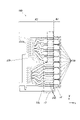
- the configuration of the electronic device 1 of the first embodiment will be described with reference to FIGS. 1 and 2.
- the electronic device 1 includes a wiring substrate 100 and an electronic component 200. Further, the electronic device 1 includes a lid 30 for sealing the wiring substrate 100.
- the wiring substrate 100 includes a main body 20 and a terminal member 10 extending to the outside of the main body 20.
- the electronic device 1 includes the lid body 30, it can be said that the lid body 30 seals the main body 20.
- the wiring board 100 is a package for an electronic device in which the electronic component 200 is mounted inside the main body 20 and the electronic component 200 and the wiring of the external board 2 are electrically connected via the terminal member 10.
- the wiring substrate 100 of the present embodiment mounts, for example, an electronic component 200 for optical communication.
- the electronic component 200 is an electronic component, for example, a light emitting element or a light receiving element, to which a high frequency signal related to optical communication (for example, a modulation rate of about 96 Gbad or less and a frequency band of about 75 GHz or less) is input or output. Can be done.
- a high frequency signal related to optical communication for example, a modulation rate of about 96 Gbad or less and a frequency band of about 75 GHz or less
- the mounted electronic component 200 is not limited to the above.
- the main body 20 includes a bottom portion 21, a frame body 22, and a seal ring 23.
- the bottom portion 21 is a rectangular plate-shaped member.
- the directions parallel to the rectangular side of the bottom portion 21 are the X direction and the Y direction, and the direction perpendicular to the bottom portion 21 and toward the lid 30 is the Z direction.
- the surface facing the + Z direction is referred to as "upper surface”
- the surface facing the ⁇ Z direction is referred to as “lower surface”.
- the layer relatively on the ⁇ Z direction side is referred to as “lower layer”.
- planar view viewing from the Z direction is referred to as “planar view”, and viewing through other members from the Z direction is referred to as “planar perspective”.
- a mounting area on which the electronic component 200 is mounted is provided on the upper surface of the bottom portion 21, and wiring that is electrically connected to the terminal of the electronic component 200 mounted on the mounting area is formed. There is.
- the frame body 22 is a frame-shaped member provided at a position surrounding the mounting area of the electronic component 200 in a plan view.
- the frame body 22 extends in the + Z direction from the outer peripheral portion of the bottom portion 21 to form a frame-shaped side wall.
- the frame 22 may be formed with a through hole 22a for passing an optical fiber or the like.
- the bottom portion 21 and the frame body 22 can be configured, for example, in which a plurality of insulating substrates are laminated in the Z direction.
- a ceramic sintered body such as an aluminum oxide sintered body, an aluminum nitrided sintered body, a silicon carbide sintered body, a mulite sintered body, or glass ceramics can be used.
- the frame body 22 may be a member separate from the bottom portion 21, or may be integrally formed with the bottom portion 21.
- the seal ring 23 is located on the upper surface of the frame body 22.
- the seal ring 23 can be used as a sealing material when the main body 20 is airtightly sealed by using the lid 30 after mounting the electronic component 200 on the bottom portion 21.
- the seal ring 23 is formed by, for example, brazing a frame-shaped metal plate containing a metal plate of Fe—Ni alloy or Fe—Ni—Co alloy in a frame-shaped conductor formed of a conductor paste containing a refractory metal such as tungsten or molybdenum. It may be brazed and joined with a material or the like.
- the lid 30 is a plate-shaped member having substantially the same shape as the bottom 21 in a plan view.
- the lid 30 may be any as long as it can reduce the intrusion of foreign matter such as water and fine particles into the inside of the electronic device 1.
- the same metal material as the seal ring 23, or the same ceramic material as the bottom 21 and the frame 22 can be processed and molded into a plate shape.
- the space formed by the bottom portion 21, the frame body 22, and the lid body 30 will be referred to as a cavity.
- a fitting portion 22b penetrating in the thickness direction (X direction) is provided on the side wall of the frame body 22 on the + X direction side.
- the terminal member 10 has a shape to be fitted to the fitting portion 22b, is located from the inside ( ⁇ X direction side) to the outside (+ X direction side) of the fitting portion 22b, and is located at the fitting portion. It is blocking 22b.
- the terminal member 10 fitted to the fitting portion 22b is fixed to the frame body 22 by, for example, a brazing material. Further, the terminal member 10 may be a part of the laminated structure of the frame body 22.
- the terminal member 10 has a substrate 11 including a dielectric, a signal conductor 12, and a ground conductor 13.
- the portion of the terminal member 10 extending from the main body 20 has a first surface S1 facing in the + Z direction, and a part of the signal conductor 12 and a part of the ground conductor 13 are formed on the first surface S1. It is exposed.
- an external substrate 2 is connected to the first surface S1.
- the wiring located on the surface of the external substrate 2 on the ⁇ Z direction side and the signal conductor 12 and the ground conductor 13 located on the first surface S1 of the terminal member 10 are electrically connected.
- the signal conductor 12 and the ground conductor 13 are electrically connected to the terminals of the electronic component 200 via wiring formed on the bottom portion 21 and the like. In this way, the wiring of the external board 2 and the terminal of the electronic component 200 are electrically connected via the terminal member 10.
- the terminal member 10 includes a first layer 10a (FIG. 3), a second layer 10b (FIG. 4), a third layer 10c (FIGS. 5 and 6), a fourth layer 10d (FIG. 8), and a fifth layer 10e (FIG. 4). 9).
- the first layer 10a to the fifth layer 10e are laminated in the order of the first layer 10a to the fifth layer 10e in the ⁇ Z direction, and the first layer 10a is located most on the + Z direction side.
- the terminal member 10 may further have a sixth layer and a seventh layer on the ⁇ Z direction side of the fifth layer 10e.
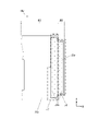
- the first layer 10a has a substrate 11a, a signal conductor 12, a grounding conductor 13a, and a through conductor 14a.
- the substrate 11a is a flat plate-shaped dielectric and has a first surface S1 (upper surface). Further, the substrate 11a is located near the outer side (the side extending in the Y direction at the end on the + X direction side) on the first surface S1, and the first region R1 on which the external substrate 2 is mounted and the first region. It has a second region R2 other than R1.
- the first region R1 of the substrate 11a is a rectangular region long in the Y direction in a plan view and is exposed to the outside of the wiring substrate 100.
- the external board 2 is connected and mounted on the first region R1.
- the mounting area r1 to which the external substrate 2 is connected is shown by a rectangular broken line in a plan view.
- the portion adjacent to the first region R1 is the frame body laminated region r2 that overlaps with the frame body 22 in a plan view.
- the second region R2 extends from the frame body laminated region r2 to the inside of the frame body 22 (that is, the inside of the cavity).
- the signal conductor 12 and the ground conductor 13a are formed on the upper surface of the substrate 11a.
- the signal conductor 12 includes the first region R1 on the first surface S1 and is located so as to extend in the first direction (X direction) away from the outer side.
- the signal conductor 12 may extend linearly in the X direction within the range of the frame body laminated region r2 of the first region R1 and the second region R2. Further, the signal conductor 12 may be curved and routed to a predetermined position at the end portion on the ⁇ X direction side within the range corresponding to the inside of the cavity in the second region R2.
- the portion of the signal conductor 12 in the first region R1 may be a rectangular signal terminal 12T.
- the signal terminal 12T has a predetermined width in the Y direction in order to make an electrical connection with the wiring of the external board 2. Further, the portion of the signal conductor 12 in the frame body laminated region r2 may have a width smaller in the Y direction than the signal terminal 12T.
- the terminal member 10 of the present embodiment has 16 signal conductors 12. The number of signal conductors 12 can be appropriately changed according to the number of terminals of the electronic component 200 to be mounted.
- the ground conductor 13a includes the first region R1 on the first surface S1 and is located so as to extend in the first direction (X direction) away from the outer side.
- the ground conductor 13a may extend linearly in the X direction within the range of the frame body laminated region r2 of the first region R1 and the second region R2. Further, the ground conductor 13a may be curved and routed to a predetermined position at the end portion on the ⁇ X direction side within the range corresponding to the inside of the cavity in the second region R2.
- the portion of the signal conductor 12 in the first region R1 may be a ground terminal 13T to which the wiring of the external board 2 is connected.
- the terminal member 10 of the present embodiment has nine ground conductors 13a, and each ground conductor 13a has a ground potential.
- the two ground conductors 13a are located on both sides of the 16 signal conductors 12, that is, at both ends on the Y direction side of the first layer 10a. Further, the remaining seven conductors are provided at positions where two signal conductors 12 are sandwiched between adjacent ground conductors 13a. That is, the ground conductor 13a, the signal conductor 12, the signal conductor 12, and the ground conductor 13a are repeatedly arranged in the Y direction.
- the number of ground conductors 13 can be appropriately changed according to the number of terminals of the electronic component 200 to be mounted.
- a groove 15 may be formed in the substrate 11a between two adjacent signal terminals 12T without sandwiching the ground terminal 13T. Since the formed portion of the groove 15 is filled with air and the relative permittivity is lowered, the electric field coupling between the two signal terminals 12T becomes weaker as compared with the case where the groove 15 is not provided.
- the groove 15 may be formed up to the end of the substrate 11a, or may be formed only between the signal terminals 12T. This makes it possible to reduce adverse effects due to electromagnetic interference such as crosstalk noise between the signal terminals 12T.
- the wiring substrate 100 having such a configuration is excellent in transmission characteristics of high frequency signals.
- a plurality of through conductors 14a penetrating the substrate 11a in the Z direction may be connected to each ground conductor 13a.
- the position of the through conductor 14 is indicated by circular dots.
- the penetrating conductors 14 are formed at regular intervals along the contour of the grounding conductor 13a in a region overlapping the grounding conductor 13a in plan perspective.
- a through conductor 14 is formed between two signal conductors 12 adjacent to each other without sandwiching the ground conductor 13a.
- the through conductor 14a may have, for example, a cylindrical shape, but is not limited to this shape. The same applies to the through conductors 14b to 14e described later.
- the second layer 10b has a flat plate-shaped substrate 11b containing a dielectric, a grounding conductor 13b, and a through conductor 14b.
- the substrate 11b has a first region R1 and a second region R2.
- the second layer 10b overlaps with the first layer 10a so that the positions of the substrate 11b and the first region R1 of the substrate 11a coincide with each other in plan perspective.
- a portion overlapping the mounting region r1 and a portion overlapping the frame stacking region r2 in plan perspective are shown by broken lines (the same applies to FIGS. 5, 8 and 9).
- the ground conductor 13b is formed on the upper surface of the substrate 11b.
- the grounding conductor 13b has a portion that overlaps with the grounding conductor 13a of the first layer 10a in plan perspective, and has a portion that connects the ends of the portion on the ⁇ X direction side to each other.
- the ground conductor 13b has a shape obtained by removing a portion overlapping the formation region of the signal conductor 12 in the first layer 10a and a region in the vicinity thereof in the first layer 10a from the planar conductor.
- the upper surface of the ground conductor 13b is connected to the through conductor 14a of the first layer 10a.
- the grounding conductor 13b is electrically connected to the grounding conductor 13a of the first layer 10a via the through conductor 14a to have a grounding potential. Further, a plurality of through conductors 14b penetrating the substrate 11b in the Z direction are connected to the ground conductor 13b.
- the second layer 10b is mainly provided for adjusting the thickness between the first layer 10a and the third layer 10c or adjusting the impedance of the terminal member 10. Therefore, it can be omitted when the thickness adjustment or the impedance adjustment is unnecessary.
- the third layer 10c has a flat plate-shaped substrate 11c containing a dielectric, a grounding conductor 13c (first grounding conductor), and a through conductor 14c.
- the substrate 11c has a first region R1 and a second region R2.
- the third layer 10c overlaps with the second layer 10b so that the positions of the first region R1 of the substrate 11c and the substrate 11b coincide with each other in plan perspective. Further, the shape of the substrate 11c is substantially the same as the shape of the substrate 11b.
- the ground conductor 13c is formed on the upper surface of the substrate 11c.
- the ground conductor 13c is located at a position where the distance from the signal conductor 12 in the direction perpendicular to the first surface S1 (Z direction) is less than ⁇ / 4, when the wavelength of the high frequency signal transmitted by the signal conductor 12 is ⁇ . It is provided in.
- the ground conductor 13c has a portion that overlaps with the ground conductor 13b of the second layer 10b in plan perspective. Further, the ground conductor 13c is formed with a plurality of first openings 131A in the first region R1.
- the ground conductor 13c is formed with a plurality of second openings 132A within a predetermined distance range in the ⁇ X direction from the boundary with the first region R1 of the second region R2.
- the second opening 132A is formed in the portion overlapping the frame stacking region r2 in plan perspective, and on the + Y direction side of the third layer 10c from the center in the Y direction, -X than the frame stacking region r2.
- a second opening 132A is also formed on the directional side, that is, inside the cavity.
- the first opening 131A and the second opening 132A are arranged in a matrix so as to be adjacent to each other in the X direction and the Y direction.
- the ground conductor 13c is formed with a mesh-shaped first opening 131A and a second opening 132A.
- the ground conductor 13c has a first grid portion 131 sandwiched by adjacent first openings 131A and a second grid portion 132 sandwiched by adjacent second openings 132A.
- the first grid portion 131 and the second grid portion 132 are linear conductors extending in the X direction and the Y direction.
- the ground conductor 13c also has a linear lattice portion extending in the Y direction sandwiched between the adjacent first opening 131A and the second opening 132A at the boundary between the first region R1 and the second region R2.
- the ground conductor 13c is formed with 16 rows of openings corresponding to the 16 signal conductors 12.
- Each aperture row overlaps one signal conductor 12 in planar fluoroscopy.
- the center of the opening row in the Y direction and the signal conductor 12 overlap each other. Therefore, the first lattice portion 131 extending in the Y direction sandwiched by the first openings 131A adjacent to each other in the X direction in the opening row is orthogonal to the signal conductor 12 in plan perspective.
- the second lattice portion 132 extending in the Y direction sandwiched by the second openings 132A adjacent to each other in the X direction in the opening row is orthogonal to the signal conductor 12 in plan perspective.
- the ground conductor 13c has the first grid portion 131 at a position (first position) overlapping the first region R1 and at least a part of the signal conductor 12 in plan perspective.
- the ground conductor 13c is connected to the first grid portion 131 in the X direction, and has the second grid portion 132 at a position (second position) overlapping the second region R2 and at least a part of the signal conductor 12 in plan perspective. ..
- the upper surface of the ground conductor 13c is connected to the through conductor 14b of the second layer 10b. Therefore, the ground conductor 13c is electrically connected to the ground conductor 13b of the second layer 10b via the through conductor 14b to have a ground potential. Further, a plurality of through conductors 14c penetrating the substrate 11c in the Z direction are connected to the ground conductor 13c.
- the shapes of the first opening 131A and the second opening 132A in the third layer 10c, and the arrangement of the through conductor 14c will be described in detail.
- the first opening 131A and the second opening 132A have a rectangular shape having sides in the X direction (first direction) and the Y direction (second direction).
- the rectangular shape is not limited to a shape (rectangle) in which the apex angles of the four corners are exactly right angles.
- the second direction is a direction intersecting with the first direction.
- the rectangular shape includes a shape in which some corners of the rectangle are dropped to form a polygon.
- the shape in which the corners are dropped means a shape in which two sides forming the corners of the four sides of the rectangle are connected by sides that are non-parallel to either of the two sides.
- the rectangular shape may include a shape in which the sides of the rectangle are connected by a curve. Therefore, in the present disclosure, the rectangular shape is included in the design, and the shape of the opening in the case where the corner portion of the opening actually formed through the manufacturing process is curved due to the restriction in the process is also included in the rectangular shape. Is done. Further, the rectangular shape may include a shape in which a protrusion P overlapping with the through conductor 14c protrudes from a part of the sides in a plan view.
- the lengths of the first opening 131A and the second opening 132A in the X direction and the Y direction are ⁇ / 8 or more and ⁇ / 4 or less. Further, the area of each first opening 131A is larger than the area of each second opening 132A. Specifically, the first opening 131A and the second opening 132A have the same width in the Y direction, and the width of the first opening 131A in the X direction is larger than the width of the second opening 132A in the X direction.
- a through conductor 14c is located in the first lattice portion 131 and the second lattice portion 132. That is, the through conductor 14c is formed and connected at a position overlapping the first lattice portion 131 and the second lattice portion 132 in a plan view. Specifically, the through conductor 14c is located so as to overlap the portion of the first lattice portion 131 extending in the X direction. Further, the through conductor 14c is located at the boundary between the first region R1 and the second region R2 so as to overlap the lattice portion extending in the Y direction. Further, the through conductor 14c is located at the intersection of the second lattice portion 132.
- the through conductor 14c is also located around the first opening 131A and the second opening 132A.
- Each through conductor 14c has a distance of less than ⁇ / 4 from the adjacent through conductor 14c. That is, when focusing on one through conductor 14c, at least one other through conductor 14c is located within the range of ⁇ / 4 from the through conductor 14c in the XY plane.
- the through conductor 14b of the second layer 10b is located at a position where it overlaps with a part of the through conductor 14c in a plane perspective.
- the through conductors 14b and 14c located in the second region R2 are formed at overlapping positions in plan perspective.
- the arrangement density of the through conductors 14b and 14c in the formation region of the mesh-shaped second opening 132A becomes high. It has been enhanced.
- the through conductors 14b and 14c are located in a straight line in the Z direction with the intersection of the second lattice portions 132 in between.
- a plurality of through conductors 14c are located at equal intervals in the X direction over the first region R1 and the second region R2, but the present invention is not limited to this.
- the arrangement interval of the through conductor 14c in the first region R1 may be smaller than the arrangement interval of the through conductor 14c in the second region R2.
- the arrangement density of the through conductor 14c in the first region R1 may be higher than the arrangement density of the through conductor 14c in the second region R2.
- the through conductor 14c may be located at the intersection of the first lattice portion 131.
- the fourth layer 10d has a flat plate-shaped substrate 11d containing a dielectric, a grounding conductor 13d (second grounding conductor), and a through conductor 14d.
- the substrate 11d has a first region R1 and a second region R2.
- the fourth layer 10d overlaps with the third layer 10c so that the positions of the first region R1 of the substrate 11d and the substrate 11c coincide with each other in plan perspective. Further, the shape of the substrate 11d near the end in the + X direction is substantially the same as the shape of the substrate 11c.
- the ground conductor 13d is formed on the upper surface of the substrate 11d.
- the ground conductor 13d is provided at a position where the distance from the signal conductor 12 in the Z direction is less than ⁇ / 4. Since the ground conductor 13d is farther from the first surface S1 than the ground conductor 13c of the third layer 10c, the distance between the first surface S1 and the ground conductor 13d is larger than the distance between the first surface S1 and the ground conductor 13c. big.
- each third opening 133A is the same as the shape and area of the first opening 131A of the third layer 10c. Therefore, the third opening 133A has a rectangular shape having sides in the X and Y directions, and the length in the X and Y directions is ⁇ / 8 or more and ⁇ / 4 or less. Each third opening 133A overlaps with the first opening 131A in a plan view.
- the ground conductor 13d has a third grid portion 133 sandwiched by adjacent third openings 133A.
- the third lattice portion 133 is a linear conductor extending in the X direction and the Y direction.
- a further opening may be formed in the ground conductor 13d at a position overlapping the second opening 132A of the third layer 10c. Further, the area of the third opening 133A may be smaller than the area of the first opening 131A within the range where the length of the third opening 133A in the X direction and the Y direction is ⁇ / 8 or more and ⁇ / 4 or less. ..
- the upper surface of the ground conductor 13d is connected to the through conductor 14c of the third layer 10c. Therefore, the ground conductor 13d is electrically connected to the ground conductor 13c of the third layer 10c via the through conductor 14c to have a ground potential. Further, a plurality of through conductors 14d penetrating the substrate 11d in the Z direction are connected to the ground conductor 13d.
- the fifth layer 10e has a flat plate-shaped substrate 11e containing a dielectric, a ground conductor 13e, and a through conductor 14e.
- the substrate 11e has a first region R1 and a second region R2.
- the fifth layer 10e overlaps with the fourth layer 10d so that the positions of the first region R1 of the substrate 11e and the substrate 11d coincide with each other in plan perspective.
- the shape of the substrate 11e is substantially the same as the shape of the substrate 11d.
- the upper surface of the ground conductor 13e is connected to the through conductor 14d of the fourth layer 10d. Therefore, the ground conductor 13e is electrically connected to the ground conductor 13d of the fourth layer 10d via the through conductor 14d to have a ground potential.
- the ground conductor 13e is a solid conductor formed in a region including a position overlapping with the third opening 133A of the fourth layer 10d in a plan view. The ground conductor 13e is located over a part of the mounting area r1 and the frame body laminated area r2.
- a plurality of through conductors 14e penetrating the substrate 11e in the Z direction are connected to the ground conductor 13e.
- the through conductor 14e is connected to the grounding conductor of the sixth layer below the through conductor 14e.
- the grounding conductor of the sixth layer may be further connected to the grounding conductor of the seventh layer of the lower layer by a penetrating conductor penetrating the substrate of the sixth layer. In this way, the ground potential can be stabilized by electrically connecting a plurality of layers of ground conductors via the through conductors.
- the through conductor 14e can be omitted.
- the base 11 of the terminal member 10 has the bases 11a to 11e provided in the first layer 10a to the fifth layer 10e.
- the grounding conductor 13 of the terminal member 10 has grounding conductors 13a to 13e provided in the first layer 10a to the fifth layer 10e.
- the ground conductors 13b to 13e are located inside the substrate 11.
- the microstrip line is composed of the signal conductor 12 of the first layer 10a and the ground conductors 13b to 13e below the signal conductor 12.
- the terminal member 10 can be manufactured, for example, by the following method.
- a ceramic sintered body such as an aluminum oxide sintered body, an aluminum nitrided sintered body, a silicon carbide sintered body, a mulite sintered body, or glass ceramics can be applied.
- the substrate 11 of the terminal member 10 can be manufactured as follows. First, a raw material powder containing aluminum oxide powder and a powder such as silicon oxide as a sintering aid component as a main component is kneaded with an organic solvent and a binder to form a slurry.
- this slurry is molded into a sheet by a molding method such as a doctor blade method or a lip coater method to prepare ceramic green sheets (hereinafter, also referred to as green sheets) to be substrates 11a to 11e.
- a molding method such as a doctor blade method or a lip coater method to prepare ceramic green sheets (hereinafter, also referred to as green sheets) to be substrates 11a to 11e.
- a plurality of green sheets are laminated to prepare a laminated body.
- the substrate 11 can be manufactured by firing this laminate at a temperature of about 1300 ° C to 1600 ° C.
- the signal conductor 12 on the substrate 11a and the ground conductors 13a to 13e on the substrates 11a to 11e are made of a metal material such as tungsten, molybdenum, manganese or copper, or an alloy material of these metal materials as a conductor component. Included as.
- a metal paste prepared by mixing tungsten powder with an organic solvent and an organic binder is printed at a predetermined position on a green sheet by a screen printing method or the like. It can be formed by firing.
- the through conductors 14a to 14e are provided with through holes at predetermined positions on the green sheet prior to printing the above metal paste, and the same metal paste as above is filled in the through holes and fired together with the green sheet. It can be formed by doing.
- a nickel film of about 1 to 10 ⁇ m and a gold film of about 0.1 to 3 ⁇ m are sequentially formed to protect the surface and protect the surface. , It is possible to improve the bondability of brazing material, solder, etc.
- the impedance of the terminal member 10 can be adjusted to an appropriate value. This will be described below.
- the resonance frequency shifts to the high frequency side, so that the transmission characteristic of the high frequency signal becomes good.
- a mesh-shaped first opening 131A is formed in the grounding conductor 13c under the signal conductor 12 in the mounting region r1 (first region R1).
- a wiring substrate 100 is excellent in transmission characteristics of high frequency signals.
- a mesh-shaped second opening 132A is further formed on the cavity side of the mounting region r1, that is, inside the frame body laminated region r2 and the cavity.
- the frequency of resonance generated around the mounting region r1 can be shifted to the high frequency side, so that the wiring substrate 100 having such a configuration is excellent in the transmission characteristics of the high frequency signal.
- the decrease in impedance can be further reduced.
- the resonance frequency of a microstrip line is largely controlled by the wiring cross-sectional shape of the surface perpendicular to the signal propagation direction. Therefore, in the resonance frequency adjustment, the signal conductor and the ground conductor within the range of the mounting region r1 are usually used. The shape is the adjustment target.
- the electromagnetic field generated in the mounting region r1 also spreads in the direction of the cavity, and the conductor shape extending in the direction parallel to the signal propagation direction, that is, the conductor shape extending from the mounting region r1 to the inside of the cavity also affects the resonance frequency. give. Therefore, the wiring substrate 100 having the mesh-shaped second opening 132A formed on the ground conductor 13 on the cavity side of the mounting region r1 is excellent in the transmission characteristic of the high frequency signal.
- a mesh-shaped third opening 133A is formed in the mounting region r1 also in the fourth layer 10d.
- a mesh-like opening is formed over two layers.
- the decrease in impedance can be further reduced.
- the signal conductor 12 is the signal terminal 12T in the mounting region r1, and the line width (width in the Y direction in FIG. 3) of the signal terminal 12T is for appropriately mounting the external board 2.
- the lower limit is set by design requirements. Therefore, the impedance may be smaller than the desired value.
- the decrease in impedance can be reduced and adjusted to a desired value. Further, by making the area of the first opening 131A larger than the area of the second opening 132A, the decrease in impedance can be similarly reduced. On the other hand, since there is no restriction on the line width of the signal conductor 12 on the cavity side of the mounting region r1, for example, in the frame laminated region r2, the decrease in impedance can be reduced by making the signal conductor 12 thinner. Therefore, in the third layer 10c, the area of the second opening 132A may be smaller than the area of the first opening 131A.
- no opening is formed in the range of the second region R2 including the frame body laminated region r2.
- the present invention is not limited to this configuration, and an opening may be formed in the second region R2 of the fourth layer 10d to further adjust the impedance, if necessary.
- the electromagnetic wave generated in response to the transmission of the high frequency signal can be made difficult to pass through. Thereby, the radiation of the electromagnetic wave to the outside can be reduced. Further, by reducing the length of the aperture to ⁇ / 4 or less, the shift of the resonance frequency to the low frequency side can be reduced.
- the wiring substrate 100 having such a configuration is excellent in transmission characteristics of high frequency signals.
- the impedance can be adjusted in consideration of the effective relative permittivity of the portion where each opening is formed. This will be described below.
- the smaller the mesh-like opening the more the resonance frequency can be shifted to the high frequency side.
- the smaller the mesh-like opening the lower the impedance. Therefore, there is a demand to make the aperture as large as possible while maintaining the resonance frequency high by setting the length of the aperture to ⁇ / 4 or less.
- the effective relative permittivity is lower than in the frame body laminated region r2 in which the ceramic frame 22 is in contact, so that the wavelength ⁇ in the electromagnetic wave of the same frequency becomes large. Therefore, the first opening 131A formed in the mounting region r1 is opened more than the second lattice portion 132 formed in the frame laminated region r2 while satisfying the condition that the opening length is ⁇ / 4 or less. You can make it bigger. Therefore, it is possible to reduce the decrease in impedance without shifting the resonance frequency to the low frequency side.
- the wiring substrate 100 having such a configuration is excellent in transmission characteristics of high frequency signals.
- the ground conductor 13c in which the first opening 131A and the second opening 132A are formed and the ground conductor 13d in which the third opening 133A is formed are provided at positions where the distance from the signal conductor 12 is less than ⁇ / 4. Therefore, a mesh-like opening can be formed within the range in which the electromagnetic wave propagates. Therefore, since the decrease in impedance can be reduced, the wiring substrate 100 having such a configuration is excellent in the transmission characteristic of the high frequency signal.
- the grounding conductor 13e is located in the lower layer of the grounding conductor 13d in which the third opening 133A is formed, and the grounding conductor 13e is solid formed in the region including the position where the grounding conductor 13e overlaps with the third opening 133A in a plan view. It is a conductor. Thereby, the radiation of the electromagnetic wave passing through the first opening 131A and the third opening 133A to the outside of the electronic device 1 can be reduced.
- ground conductors 13c and 13d having the mesh-like openings are electrically connected by the through conductor 14c, the ground potential can be stabilized (enhanced), so that the transmission characteristics of the high frequency signal can be improved. Can be improved. Further, since the grounding conductors 13c and 13d are further electrically connected to the grounding conductors 13a, 13b and 13e (and the grounding conductors of the sixth and seventh layers below) by other through conductors, the grounding conductors 13c and 13d are electrically connected to the grounding conductors 13a, 13b and 13e. The ground potential can be further stabilized.
- the electromagnetic wave generated by the transmission of the high frequency signal leaks in the cavity direction. Can be reduced.
- the electromagnetic wave is generated. Leakage can be reduced.
- the through conductor 14c is made denser. Can be placed. From the viewpoint of reducing the leakage of electromagnetic waves, it is desirable that the arrangement density of the through conductor 14c is high. Further, by setting the distance between the through conductors to less than ⁇ / 4, it is possible to increase the electrical connection strength between the ground conductors via the through conductors and stabilize the ground potential.
- FIGS. 10 and 11 the simulation results of the reflection loss and the insertion loss of the wiring substrate 100 of the present embodiment will be described.
- the simulation results of the embodiment in which the mesh-shaped first opening 131A, second opening 132A, and third opening 133A of the present embodiment are provided are shown by solid lines. Further, the simulation result of the comparative example in which the ground conductor 13 of the terminal member 10 is not provided with the mesh-shaped opening is shown by the broken line.
- the reflection loss of the example (the closer to 0, the larger the reflection with respect to the incident) was lower than the reflection loss of the comparative example.
- the insertion loss of the example (the loss becomes larger as the absolute value of the value is larger) is lower than the insertion loss of the comparative example.
- the wiring substrate 100 of the present embodiment includes the substrate 11, the signal conductor 12, and the ground conductor 13 including the ground conductor 13c as the first ground conductor.
- the substrate 11 has a first surface S1, a first region R1 located near the outer side of the first surface S1 on which the external substrate 2 is mounted, and a second region R2 other than the first region R1.
- the signal conductor 12 includes the first region R1 on the first surface S1 and is located so as to extend in the X direction away from the outer side.
- the ground conductor 13c is located inside the substrate 11 and the distance from the signal conductor 12 in the direction perpendicular to the first surface S1 is less than 1/4 of the wavelength ⁇ of the high frequency signal transmitted by the signal conductor 12.
- the ground conductor 13c has a first lattice portion 131 sandwiched by the first opening 131A at a first position overlapping the first region R1 and at least a part of the signal conductor 12 in a plane perspective toward the first surface S1.
- the first opening 131A has a length of ⁇ / 8 or more and ⁇ / 4 or less in the X direction and the Y direction, and a through conductor 14c is located in the first lattice portion 131.
- the first opening 131A can be made into a desired area by a simple design.
- the through conductor 14c can be arranged at a higher density.
- the ground conductor 13c is connected to the first grid portion 131 in the X direction, and has a second grid portion 132 sandwiched by the second opening 132A at a second position overlapping the second region R2 in plan perspective.
- the length of the second opening 132A in the X direction and the Y direction is ⁇ / 8 or more and ⁇ / 4 or less, and the area of the second opening 132A is smaller than the area of the first opening 131A.
- the frequency of resonance generated around the mounting region r1 can be shifted to the high frequency side, and the transmission characteristics of the high frequency signal can be improved.
- the decrease in impedance can be further reduced.
- the impedance can be adjusted in consideration of the effective relative permittivity of the portion where each opening is formed.
- the second opening 132A can be made into a desired area by a simple design.
- the through conductor 14c can be arranged at a higher density.
- the ground conductor 13 is located inside the substrate 11 and the distance from the signal conductor 12 in the direction perpendicular to the first surface S1 is less than ⁇ / 4. Then, a ground conductor 13d as a second ground conductor having a third lattice portion 133 sandwiched by the third opening 133A is provided at a third position overlapping the first region R1 and at least a part of the signal conductor 12 in plan perspective. .. Further, the third opening 133A has a length of ⁇ / 8 or more and ⁇ / 4 or less in the X direction and the Y direction.
- grounding conductor 13d is separated from the grounding conductor 13c from the first surface S1 in the direction perpendicular to the first surface S1, and is connected to the grounding conductor 13c by the through conductor 14c.
- a mesh-like opening can be formed over the two layers, so that a decrease in impedance can be further reduced.
- the ground potential can be stabilized by increasing the electrical connection strength between the ground conductors.
- the third opening 133A can be made into a desired area by a simple design.
- the third opening 133A overlaps with the first opening 131A in a plane perspective.
- a mesh-like opening can be formed over the two layers, so that a decrease in impedance can be reduced.
- the area of the third opening 133A smaller than the area of the first opening 131A, it is possible to increase the degree of freedom in design for adjusting the resonance frequency while adjusting the impedance to a desired range. .. Since the fourth layer 10d in which the third opening 133A is formed is farther from the signal conductor 12 than the third layer 10c in which the first opening 131A is formed, such adjustment is possible.
- the wiring substrate 100 has a plurality of through conductors 14c, and the through conductor 14c has a distance of less than ⁇ / 4 from the adjacent through conductor 14c.
- the ground potential can be stabilized by increasing the electrical connection strength between the ground conductors via the through conductor.
- the electronic device 1 according to the present embodiment includes the above wiring base 100 and the electronic component 200 connected to the wiring base 100, it is excellent in transmission characteristics of high frequency signals.
- the second embodiment will be described.
- the structure of the terminal member 10 is different from that of the first embodiment.
- the differences from the first embodiment will be described.
- the electronic device 1 and the wiring substrate 100 of the second embodiment can be used for optical communication applications in a higher frequency band (for example, a modulation rate of about 128 Gbaud or less and a frequency band of about 95 GHz or less).
- the configuration of the terminal member 10 according to the second embodiment will be described with reference to FIG. 12.
- the terminal member 10 of the second embodiment shows an example of a four-layer structure including a first layer 10a, a second layer 10b, a third layer 10c, and a fourth layer 10d.
- the first layer 10a has a substrate 11a, eight signal conductors 12, five ground conductors 13a, and a through conductor 14a. Also in the second embodiment, the substrate 11a has a first region R1 on which the external substrate 2 is mounted and a second region R2 including the frame body laminated region r2.
- the second layer 10b has a substrate 11b, a grounding conductor 13b, and a through conductor 14b.
- the ground conductor 13b corresponds to the "first ground conductor”.
- the ground conductor 13b is formed with a first opening 131A in the first region R1. That is, the ground conductor 13b has a first grid portion 131 sandwiched by the first opening 131A.
- the second opening 132A is not formed in the ground conductor 13b, but the second opening 132A may be formed if necessary for impedance adjustment.
- the third layer 10c has a substrate 11c and a ground conductor 13c.
- the ground conductor 13c corresponds to the "second ground conductor”.
- the ground conductor 13c is formed with a third opening 133A that overlaps with the first opening 131A in plan perspective. That is, the ground conductor 13c has a third lattice portion 133 sandwiched by the third opening 133A.
- the third layer 10c does not have a through conductor.
- the fourth layer 10d is made of a dielectric substrate 11d and does not have conductors such as a ground conductor and a through conductor.
- the first opening 131A or the third opening 133A does not overlap with the ground conductor 13 in plan perspective.
- the solid conductor is not provided at a position overlapping the first opening 131A or the third opening 133A in plan perspective.
- the resonance frequency can be further shifted to the high frequency side to improve the transmission characteristics of the high frequency signal.
- the resonance frequency becomes high, the cavity resonance in which a standing wave is generated in the cavity is likely to occur, and this cavity resonance can be reduced by not providing a solid conductor (not shielding) in the lowermost layer. can.
- deterioration of the transmission characteristics of the high frequency signal due to the influence of the cavity resonance can be reduced, and the resonance frequency can be further shifted to the high frequency side.
- FIG. 13 is an enlarged view showing a part of the terminal member 10, and among the terminal members 10, a first layer 10a and a second layer 10b overlapping the lower surface of the first layer 10a are shown.
- a plurality of signal conductors 12 are formed on the upper surface of the substrate 11a of the first layer 10a.
- a ground conductor 13b is formed on the upper surface of the substrate 11b of the second layer 10b.
- a groove 15 that penetrates the substrate 11a in the Z direction is provided between the two adjacent signal conductors 12 of the substrate 11a.
- the substrate 11 of the terminal member 10 has a groove 15 penetrating from the first surface S1 to the forming layer of the ground conductor 13b as the first ground conductor.
- the groove 15 is an oval shape long in the extending direction (X direction) of the signal conductor 12, but the shape is not limited to this and may be a rectangle or the like. Further, the groove 15 may be a notch extending to the end portion of the substrate 11a.
- a part of the ground conductor 13b overlaps with the signal conductor 12 in plan perspective.
- a plurality of mesh-shaped first openings 131A are formed in the ground conductor 13b. A part of the first opening 131A overlaps the signal conductor 12 in plan perspective.
- a part of the first opening 131A overlaps the groove 15 in plan perspective.
- a part of the first opening 131A is exposed from the groove 15 when viewed from the Z direction (that is, in a planar perspective toward the first surface S1).
- a part of the grounding conductor 13b of the second layer 10b is exposed from the groove 15.
- the groove 15 may have a T-shape. Specifically, a shape in which the groove 15 is arranged on the extension line of the signal conductor 12 in the signal transmission direction is preferable. Specifically, the groove 15 has a portion extending in the X direction (signal transmission direction) between two adjacent signal conductors 12 and a portion extending in the X direction from the end portion on the + X direction side in the + Y direction. It is preferable to have a portion extending in the ⁇ Y direction and a portion extending in the ⁇ Y direction from the end portion.
- the portion of the groove 15 extending in the + Y direction and the portion extending in the ⁇ Y direction reach a position overlapping the extended portion when the signal conductor 12 is assumed to be extended in the + X direction, respectively. It is preferable that it is extended.
- the signal conductor 12 is connected to an FPC or the like which is an external board, it is possible to reduce the decrease in impedance of the signal conductor 12 in the vicinity of the connection portion due to the connection with the external board. This makes it possible to improve the high frequency characteristics of the signal conductor 12, particularly the high frequency characteristics in the common mode.
- the first opening 131A, the second opening 132A, and the third opening 133A are assumed to have a rectangular shape having sides in the X direction and the Y direction, but the present invention is not limited to this.
- the first opening 131A, the second opening 132A, and the third opening 133A may have a shape having sides in the first and second directions that are not orthogonal to each other, for example, a parallelogram or a rhombus.
- the first opening 131A, the second opening 132A, and the third opening 133A may be a polygon other than a rectangular shape, a circular shape, an elliptical shape, or the like.
- any one or two of the first opening 131A, the second opening 132A and the third opening 133A may be rectangular, and the rest may be non-rectangular as exemplified above.
- the present invention is not limited to this, and the number of layers in which the mesh-like opening is formed is one layer or three or more layers. You may.
- This disclosure can be used for wiring substrates and electronic devices.
Landscapes
- Engineering & Computer Science (AREA)
- Microelectronics & Electronic Packaging (AREA)
- Physics & Mathematics (AREA)
- Electromagnetism (AREA)
- Structure Of Printed Boards (AREA)
- Production Of Multi-Layered Print Wiring Board (AREA)
Priority Applications (5)
| Application Number | Priority Date | Filing Date | Title |
|---|---|---|---|
| EP21875557.7A EP4224519A4 (en) | 2020-09-30 | 2021-09-28 | WIRING BASE AND ELECTRONIC DEVICE |
| JP2022553973A JP7428821B2 (ja) | 2020-09-30 | 2021-09-28 | 配線基体および電子装置 |
| US18/029,023 US20240074035A1 (en) | 2020-09-30 | 2021-09-28 | Wiring base and electronic device |
| CN202180066107.4A CN116235293A (zh) | 2020-09-30 | 2021-09-28 | 布线基体以及电子装置 |
| JP2024009105A JP7813823B2 (ja) | 2020-09-30 | 2024-01-25 | 配線基体および電子装置 |
Applications Claiming Priority (2)
| Application Number | Priority Date | Filing Date | Title |
|---|---|---|---|
| JP2020165236 | 2020-09-30 | ||
| JP2020-165236 | 2020-09-30 |
Publications (1)
| Publication Number | Publication Date |
|---|---|
| WO2022071256A1 true WO2022071256A1 (ja) | 2022-04-07 |
Family
ID=80950381
Family Applications (1)
| Application Number | Title | Priority Date | Filing Date |
|---|---|---|---|
| PCT/JP2021/035477 Ceased WO2022071256A1 (ja) | 2020-09-30 | 2021-09-28 | 配線基体および電子装置 |
Country Status (5)
| Country | Link |
|---|---|
| US (1) | US20240074035A1 (https=) |
| EP (1) | EP4224519A4 (https=) |
| JP (2) | JP7428821B2 (https=) |
| CN (1) | CN116235293A (https=) |
| WO (1) | WO2022071256A1 (https=) |
Cited By (2)
| Publication number | Priority date | Publication date | Assignee | Title |
|---|---|---|---|---|
| CN115343812A (zh) * | 2022-08-22 | 2022-11-15 | 德阳三环科技有限公司 | 输入输出构件和制备方法及封装基座和光器件 |
| WO2026048794A1 (ja) * | 2024-08-29 | 2026-03-05 | 京セラ株式会社 | 配線基板、電子部品収納用パッケージ及び電子モジュール |
Citations (3)
| Publication number | Priority date | Publication date | Assignee | Title |
|---|---|---|---|---|
| JPH05267913A (ja) * | 1992-03-17 | 1993-10-15 | Shinko Electric Ind Co Ltd | 高周波用電子部品の信号線路 |
| JP2006086293A (ja) * | 2004-09-15 | 2006-03-30 | Canon Inc | プリント配線基板及び該配線基板のグランドパターン設計方法 |
| JP2019129287A (ja) * | 2018-01-26 | 2019-08-01 | 住友電気工業株式会社 | 光受信モジュール用パッケージ |
Family Cites Families (12)
| Publication number | Priority date | Publication date | Assignee | Title |
|---|---|---|---|---|
| US6891731B1 (en) * | 1999-11-01 | 2005-05-10 | Advanced Micro Devices, Inc. | Crosstalk cancellation for integrated circuit package configuration |
| US6624729B2 (en) * | 2000-12-29 | 2003-09-23 | Hewlett-Packard Development Company, L.P. | Slotted ground plane for controlling the impedance of high speed signals on a printed circuit board |
| KR101454720B1 (ko) * | 2010-12-03 | 2014-10-27 | 가부시키가이샤 무라타 세이사쿠쇼 | 고주파 신호선로 및 전자기기 |
| JP5842850B2 (ja) * | 2012-06-29 | 2016-01-13 | 株式会社村田製作所 | フラットケーブルおよび電子機器 |
| JP6272131B2 (ja) * | 2014-05-02 | 2018-01-31 | 日本電信電話株式会社 | 光モジュール |
| WO2015182348A1 (ja) * | 2014-05-29 | 2015-12-03 | 株式会社村田製作所 | 高周波信号線路及びこれを備えた電子機器 |
| WO2016186128A1 (ja) * | 2015-05-20 | 2016-11-24 | 京セラ株式会社 | 半導体素子パッケージ、半導体装置および実装構造体 |
| JP6441850B2 (ja) * | 2016-03-31 | 2018-12-19 | Ritaエレクトロニクス株式会社 | 多層プリント配線板 |
| JP6724648B2 (ja) * | 2016-08-16 | 2020-07-15 | 富士ゼロックス株式会社 | 配線基板 |
| JP6825986B2 (ja) * | 2017-05-26 | 2021-02-03 | 京セラ株式会社 | 配線基板、電子部品収納用パッケージおよび電子装置 |
| JP7100487B2 (ja) * | 2018-04-27 | 2022-07-13 | 京セラ株式会社 | 印刷配線板 |
| JP7145311B2 (ja) * | 2019-03-07 | 2022-09-30 | 京セラ株式会社 | 配線基板、電子部品用パッケージおよび電子装置 |
-
2021
- 2021-09-28 US US18/029,023 patent/US20240074035A1/en active Pending
- 2021-09-28 JP JP2022553973A patent/JP7428821B2/ja active Active
- 2021-09-28 WO PCT/JP2021/035477 patent/WO2022071256A1/ja not_active Ceased
- 2021-09-28 CN CN202180066107.4A patent/CN116235293A/zh active Pending
- 2021-09-28 EP EP21875557.7A patent/EP4224519A4/en active Pending
-
2024
- 2024-01-25 JP JP2024009105A patent/JP7813823B2/ja active Active
Patent Citations (3)
| Publication number | Priority date | Publication date | Assignee | Title |
|---|---|---|---|---|
| JPH05267913A (ja) * | 1992-03-17 | 1993-10-15 | Shinko Electric Ind Co Ltd | 高周波用電子部品の信号線路 |
| JP2006086293A (ja) * | 2004-09-15 | 2006-03-30 | Canon Inc | プリント配線基板及び該配線基板のグランドパターン設計方法 |
| JP2019129287A (ja) * | 2018-01-26 | 2019-08-01 | 住友電気工業株式会社 | 光受信モジュール用パッケージ |
Non-Patent Citations (1)
| Title |
|---|
| See also references of EP4224519A4 * |
Cited By (3)
| Publication number | Priority date | Publication date | Assignee | Title |
|---|---|---|---|---|
| CN115343812A (zh) * | 2022-08-22 | 2022-11-15 | 德阳三环科技有限公司 | 输入输出构件和制备方法及封装基座和光器件 |
| CN115343812B (zh) * | 2022-08-22 | 2023-10-17 | 德阳三环科技有限公司 | 输入输出构件和制备方法及封装基座和光器件 |
| WO2026048794A1 (ja) * | 2024-08-29 | 2026-03-05 | 京セラ株式会社 | 配線基板、電子部品収納用パッケージ及び電子モジュール |
Also Published As
| Publication number | Publication date |
|---|---|
| JP7813823B2 (ja) | 2026-02-13 |
| EP4224519A1 (en) | 2023-08-09 |
| CN116235293A (zh) | 2023-06-06 |
| US20240074035A1 (en) | 2024-02-29 |
| JP2024050679A (ja) | 2024-04-10 |
| JPWO2022071256A1 (https=) | 2022-04-07 |
| EP4224519A4 (en) | 2024-10-16 |
| JP7428821B2 (ja) | 2024-02-06 |
Similar Documents
| Publication | Publication Date | Title |
|---|---|---|
| EP3780259B1 (en) | Transition structure and multilayer transition structure for millimeter wave | |
| US10790245B2 (en) | High-frequency ceramic board and high-frequency semiconductor element package | |
| CN102593565B (zh) | 电介质波导管的输入输出连接构造 | |
| JP6397127B2 (ja) | 半導体素子パッケージ、半導体装置および実装構造体 | |
| JP7813823B2 (ja) | 配線基体および電子装置 | |
| US9577310B2 (en) | Semiconductor package and semiconductor package mounting structure | |
| JP4653005B2 (ja) | 電子部品パッケージ | |
| CN104364897B (zh) | 元件收纳用封装件以及安装结构体 | |
| WO2020110610A1 (ja) | 導波管スロットアンテナ | |
| JP6973667B2 (ja) | 回路基板及び電子機器 | |
| JP5926290B2 (ja) | 入出力部材ならびに電子部品収納用パッケージおよび電子装置 | |
| JP2015056719A (ja) | 多層配線基板 | |
| JP3347607B2 (ja) | 積層型導波管線路 | |
| JP4874177B2 (ja) | 接続端子及びこれを用いたパッケージ並びに電子装置 | |
| JPH09321501A (ja) | 多層高周波回路基板 | |
| JPH1174701A (ja) | 誘電体導波管線路の接続構造 | |
| JP7431351B2 (ja) | 半導体パッケージ及び半導体電子装置 | |
| WO2022070856A1 (ja) | 配線基体および電子装置 | |
| CN113056092A (zh) | 布线基板 | |
| WO2026048794A1 (ja) | 配線基板、電子部品収納用パッケージ及び電子モジュール | |
| WO2025249455A1 (ja) | 配線基板、電子部品収納用パッケージ及び電子モジュール | |
| WO2025047422A1 (ja) | 配線基板、電子部品収納用パッケージ及び電子モジュール | |
| JP3600729B2 (ja) | 高周波回路用パッケージ | |
| JP2001189405A (ja) | 高周波用入出力端子ならびに高周波用半導体素子収納用パッケージ | |
| WO2026048792A1 (ja) | 配線基板、電子部品収納用パッケージ及び電子モジュール |
Legal Events
| Date | Code | Title | Description |
|---|---|---|---|
| 121 | Ep: the epo has been informed by wipo that ep was designated in this application |
Ref document number: 21875557 Country of ref document: EP Kind code of ref document: A1 |
|
| ENP | Entry into the national phase |
Ref document number: 2022553973 Country of ref document: JP Kind code of ref document: A |
|
| NENP | Non-entry into the national phase |
Ref country code: DE |
|
| ENP | Entry into the national phase |
Ref document number: 2021875557 Country of ref document: EP Effective date: 20230502 |