WO2022070779A1 - 電子部品、電子部品の製造方法、及びコンデンサ、コンデンサの製造方法 - Google Patents
電子部品、電子部品の製造方法、及びコンデンサ、コンデンサの製造方法 Download PDFInfo
- Publication number
- WO2022070779A1 WO2022070779A1 PCT/JP2021/032549 JP2021032549W WO2022070779A1 WO 2022070779 A1 WO2022070779 A1 WO 2022070779A1 JP 2021032549 W JP2021032549 W JP 2021032549W WO 2022070779 A1 WO2022070779 A1 WO 2022070779A1
- Authority
- WO
- WIPO (PCT)
- Prior art keywords
- electronic component
- barrier film
- capacitor
- film
- clay
- Prior art date
- Legal status (The legal status is an assumption and is not a legal conclusion. Google has not performed a legal analysis and makes no representation as to the accuracy of the status listed.)
- Ceased
Links
Images


Classifications
-
- H—ELECTRICITY
- H01—ELECTRIC ELEMENTS
- H01G—CAPACITORS; CAPACITORS, RECTIFIERS, DETECTORS, SWITCHING DEVICES, LIGHT-SENSITIVE OR TEMPERATURE-SENSITIVE DEVICES OF THE ELECTROLYTIC TYPE
- H01G2/00—Details of capacitors not covered by a single one of groups H01G4/00-H01G11/00
- H01G2/10—Housing; Encapsulation
-
- H—ELECTRICITY
- H01—ELECTRIC ELEMENTS
- H01G—CAPACITORS; CAPACITORS, RECTIFIERS, DETECTORS, SWITCHING DEVICES, LIGHT-SENSITIVE OR TEMPERATURE-SENSITIVE DEVICES OF THE ELECTROLYTIC TYPE
- H01G4/00—Fixed capacitors; Processes of their manufacture
- H01G4/002—Details
- H01G4/018—Dielectrics
- H01G4/06—Solid dielectrics
- H01G4/14—Organic dielectrics
- H01G4/18—Organic dielectrics of synthetic material, e.g. derivatives of cellulose
-
- H—ELECTRICITY
- H01—ELECTRIC ELEMENTS
- H01G—CAPACITORS; CAPACITORS, RECTIFIERS, DETECTORS, SWITCHING DEVICES, LIGHT-SENSITIVE OR TEMPERATURE-SENSITIVE DEVICES OF THE ELECTROLYTIC TYPE
- H01G4/00—Fixed capacitors; Processes of their manufacture
- H01G4/002—Details
- H01G4/224—Housing; Encapsulation
-
- H—ELECTRICITY
- H01—ELECTRIC ELEMENTS
- H01G—CAPACITORS; CAPACITORS, RECTIFIERS, DETECTORS, SWITCHING DEVICES, LIGHT-SENSITIVE OR TEMPERATURE-SENSITIVE DEVICES OF THE ELECTROLYTIC TYPE
- H01G4/00—Fixed capacitors; Processes of their manufacture
- H01G4/002—Details
- H01G4/228—Terminals
-
- H—ELECTRICITY
- H01—ELECTRIC ELEMENTS
- H01G—CAPACITORS; CAPACITORS, RECTIFIERS, DETECTORS, SWITCHING DEVICES, LIGHT-SENSITIVE OR TEMPERATURE-SENSITIVE DEVICES OF THE ELECTROLYTIC TYPE
- H01G4/00—Fixed capacitors; Processes of their manufacture
- H01G4/002—Details
- H01G4/228—Terminals
- H01G4/252—Terminals the terminals being coated on the capacitive element
-
- H—ELECTRICITY
- H01—ELECTRIC ELEMENTS
- H01G—CAPACITORS; CAPACITORS, RECTIFIERS, DETECTORS, SWITCHING DEVICES, LIGHT-SENSITIVE OR TEMPERATURE-SENSITIVE DEVICES OF THE ELECTROLYTIC TYPE
- H01G4/00—Fixed capacitors; Processes of their manufacture
- H01G4/32—Wound capacitors
-
- H—ELECTRICITY
- H01—ELECTRIC ELEMENTS
- H01G—CAPACITORS; CAPACITORS, RECTIFIERS, DETECTORS, SWITCHING DEVICES, LIGHT-SENSITIVE OR TEMPERATURE-SENSITIVE DEVICES OF THE ELECTROLYTIC TYPE
- H01G9/00—Electrolytic capacitors, rectifiers, detectors, switching devices, light-sensitive or temperature-sensitive devices; Processes of their manufacture
- H01G9/004—Details
- H01G9/008—Terminals
-
- H—ELECTRICITY
- H01—ELECTRIC ELEMENTS
- H01G—CAPACITORS; CAPACITORS, RECTIFIERS, DETECTORS, SWITCHING DEVICES, LIGHT-SENSITIVE OR TEMPERATURE-SENSITIVE DEVICES OF THE ELECTROLYTIC TYPE
- H01G9/00—Electrolytic capacitors, rectifiers, detectors, switching devices, light-sensitive or temperature-sensitive devices; Processes of their manufacture
- H01G9/004—Details
- H01G9/08—Housing; Encapsulation
Definitions
- Patent Document 1 describes a case-molded capacitor.
- the case-molded capacitor includes a capacitor element, a lead terminal, a mold resin, and a case.
- the capacitor element is a winding type film capacitor element and is housed in a case made of polyphenylene sulfide (PPS) resin.
- PPS polyphenylene sulfide
- the mold resin is filled in the case and seals the capacitor element.
- the lead terminal is electrically connected to the capacitor element and is led out from the mold resin part to the outside of the case.
- the method for manufacturing a capacitor according to one aspect of the present disclosure includes a step of winding a metallized film to form a winding body, a step of winding a barrier film around at least a part around the winding body, and the above-mentioned step.
- a step of spraying a metal material on both ends of the wound body around which the barrier film is wound to form an external electrode is provided.
- a clay layer is formed on the insulating film. When the barrier film is wound around the winding body, the clay layer is wound so as to face the winding body.
- the thickness of the resin case and sealing resin needs to be 2 mm or more even if it is the thinnest. Therefore, the resin case of the epoxy resin and the film capacitor using the sealing resin are heavy and tend to be very complicated in the manufacturing process. Further, when the film capacitor is an in-vehicle capacitor, the shape is custom-designed so as to be different for each vehicle model, so that it is a difficult product to reduce the cost.
- the electronic component 1 since the electronic component 1 according to the present embodiment has the clay layer 31 containing clay in the barrier film 30 covering the electronic component element 2, the electronic component 1 has a clay layer 31 of the same thickness as compared with the resin layer formed of the resin alone.
- the amount of water passing through the barrier film 30 is likely to be reduced. Therefore, the amount of water reaching the electronic component element 2 from the outside of the electronic component 1 is reduced, the moisture is less likely to act on the electronic component element 2, and the electronic component 1 having excellent moisture resistance can be easily obtained.
- the clay layer 31 can be formed on the surface of the insulating film 33 by a simple means such as coating, the manufacturing process of the electronic component 1 is less likely to be complicated, and the cost can be easily reduced.
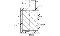
- the electronic component 1 includes an electronic component element 2 and a barrier film 30.
- the electronic component element 2 is a component or part for exhibiting the desired function of the electronic component 1.
- the electronic component element 2 has external electrodes 24 at both ends.
- the clay layer 31 is arranged so as to face the electronic component element 2. That is, it is preferable that the barrier film 30 covers the periphery of the electronic component element 2 so that the clay layer 31 is located inside (toward the electronic component element 2) when viewed from the position of the insulating film 33.
- the clay layer 31 has higher adhesion to the electronic component element 2 than the insulating film 33. Therefore, by arranging the barrier film 30 with the clay layer 31 facing toward the electronic component element 2, the clay layer 31 and the electronic component element 2 are easily brought into close contact with each other, and moisture can penetrate into the electronic component element 2. It becomes easy to reduce.
- the end face of the barrier film 30 may be covered with the external electrode 24. That is, as shown in FIG. 3B, it is preferable that the peripheral end portion 241 of the external electrode 24 is located outside the end surface in the width direction of the barrier film 30. In this case, it is preferable that the peripheral end portion 241 of the external electrode 24 covers the end surface of the barrier film 30 in the width direction over the entire circumference. In this case, by covering the boundary between the element body 2a and the barrier film 30 with the barrier film 30, it is possible to suppress the infiltration of water from the boundary portion between the element body 2a and the barrier film 30.
- the electronic component 1 may further include an exterior resin layer 4 that covers the electronic component element 2 and the barrier film 30.
- the exterior resin layer 4 has a function of protecting the electronic component element 2 and the barrier film 30 from moisture. Further, the exterior resin layer 4 may have a function of protecting the electronic component element 2 and the barrier film 30 from heat, light, electromagnetic waves, impacts, chemicals and the like.
- the exterior resin layer 4 is formed of one or both of the case (container) and the mold resin.
- the capacitor element 20 has external electrodes 24 at both ends in the axial direction.
- the external electrode 24 is preferably formed by thermal spraying of a metal material. Further, the external electrode 24 preferably contains 50% by weight or more of tin. This type of external electrode 24 is usually formed by spraying zinc, but the external electrode 24 made of zinc tends to be porous, and moisture may infiltrate from the external electrode 24. Therefore, in the present embodiment, the tin content of the external electrode 24 is increased, which makes the metal structure constituting the external electrode 24 dense and makes it difficult for water to pass through the external electrode 24, so that the capacitor element 20 The infiltration of water into the water is reduced.
- the barrier film 30 has a clay layer 31 containing clay.
- the clay layer 31 contains clay and is formed in a layered manner.
- clay is an aggregate of a plurality of mineral particles 311.
- Clay may also contain a small amount of water in an aggregate of a plurality of mineral particles 311.
- Mineral particles 311 include one or more selected from the herd of mica, vermiculite, montmorillonite, iron montmorillonite, byderite, saponite, hectorite, stepvensite, nontronite.
- the mineral particles 311 preferably contain montmorillonite, which is a highly moisture-resistant clay material.
- FIG. 2B shows a schematic perspective view of one mineral particle 311.
- the mineral particles 311 are plate-shaped or flaky particles. That is, the mineral particles 311 are particles having a thickness a smaller than the width b.
- the width b is the dimension of the longest portion of the mineral particles 311 when the mineral particles 311 are viewed from the front (viewed from directly in the thickness direction). If the mineral particle 311 is, for example, a disk, the diameter is b.
- the thickness a is a dimension in a direction orthogonal to the width b, and is a dimension between two facing surfaces of the mineral particles 311.
- P / P0 (1- ⁇ ) / (1 + 0.5A ⁇ ) ... (1)
- P / P0 indicates the specific transmittance.
- ⁇ indicates the volume fraction of the mineral particles 311 in the clay layer 31.
- A indicates the aspect ratio of the mineral particles 311.
- the barrier film 30 through which moisture does not easily pass in order to improve the moisture resistance of the capacitor 10, it is preferable to increase the volume fraction of the mineral particles 311 in the clay layer 31, and the mineral having a high aspect ratio. It is preferable to increase the content of the particles 311.
- the aspect ratio of the mineral particles 311 is preferably 20 or more. In order to obtain the clay layer 31 through which moisture does not easily pass, it is preferable to use mineral particles 311 having a higher aspect ratio, but other performances of the clay layer 31, for example, strength, adhesion and formation of the clay layer 31. The above range is preferable in consideration of easiness and the like.
- the aspect ratio of the mineral particles 311 is more preferably 100 or more, and further preferably 150 or more.
- the upper limit of the aspect ratio of the mineral particles 311 is not particularly set, and is appropriately set in consideration of the dispersibility of the mineral particles 311 in the clay layer 31 and the like.
- the content of the mineral particles 311 in the clay layer 31 is 50% by mass or more with respect to the total amount.
- the content of the mineral particles 311 is 50% by mass or more and 95% by mass or less with respect to the total amount of the clay layer 31, and the content of the binder 312 is contained.
- the ratio is preferably 5% by mass or more and 50% by mass or less with respect to the total amount of the clay layer 31. This makes it easier to obtain the clay layer 31 through which moisture does not easily pass, while ensuring the strength, adhesion, and ease of formation of the clay layer 31.
- the insulating film 33 is preferably flexible. Further, the insulating film 33 is preferably a resin film. Examples of the resin film include a film containing a synthetic resin such as polypropylene (PP), polyethylene terephthalate (PET), polyethylene naphthalate (PEN), and polyamide (nylon (registered trademark)). Thickness of the insulating film 33. Is appropriately set in consideration of electrical insulation and flexibility, but is preferably several tens of ⁇ m, more preferably 10 ⁇ m or more and 30 ⁇ m or less.
- PP polypropylene
- PET polyethylene terephthalate
- PEN polyethylene naphthalate
- nylon polyamide
- the second metallized film 72 is formed in the same manner as the first metallized film 71. That is, the second metallized film 72 has a second dielectric film 702 and a second conductive layer 712.
- the second dielectric film 702 is a long object having the same width as the first dielectric film 701.
- a second conductive layer 712 is formed on one side of the second dielectric film 702 except for the second margin portion 722.
- the second margin portion 722 is a portion where the second dielectric film 702 is exposed, and is formed along one long side of the second dielectric film 702 in a strip shape thinner than the second conductive layer 712. There is.
- the first dielectric film 701 and the second dielectric film 702 are made of, for example, polypropylene, polyethylene terephthalate, polyethylene naphthalate, polyphenyl sulfide, polystyrene, or the like.
- the first conductive layer 711 and the second conductive layer 712 are formed by a method such as a thin film deposition method or a sputtering method.
- the first conductive layer 711 and the second conductive layer 712 are made of, for example, aluminum, zinc, magnesium, or the like.
- the barrier film 30 covers the winding body 73 before forming the first external electrode 21 and the second external electrode 22 by metal spraying (metallikon) has been described, but the first is not limited to this.
- the winding body 73 may be coated with the barrier film 30.
- the first external electrode 21 and the second external electrode 22 are formed on the winding body 73.
- the winding body 73, the first external electrode 21, and the second external electrode 22 may be covered with the barrier film 30.
- the barrier film 30 covers the first external electrode 21 and the second external electrode 22.
- the winding body 73 may be coated before forming.
- the width of the barrier film 30 is increased by 1 to 2 mm from the width of the metallized films 71 and 72 forming the winding body 73, and the end portion 301 of the barrier film 30 is the axial end surface 730 of the winding body 73. Protrude more than.
- the formation of the first external electrode 21 and the second external electrode 22 by metal spraying is performed on the axial end surface 730 of the winding body 73 in the space surrounded by the end portion 301 of the barrier film 30.
- the electronic component 1 includes an electronic component element 2 having external electrodes 24 at both ends, an exterior resin layer 4 covering at least a part of the electronic component element 2, and an exterior resin layer.
- a barrier film 30 that covers at least a part of the periphery of the wall is provided. Similar to the above, the barrier film 30 has an insulating film 33 having an electrically insulating property and a clay layer 31 containing clay.
- the fourth aspect is the electronic component (1) according to any one of the first to third aspects, in which the external electrode (24) is formed by thermal spraying and contains (50)% by weight or more of tin.
- the exterior resin layer (4) makes it easier to further reduce the moisture absorption of the electronic component element (2), and the exterior resin layer (4) secures the strength of the electronic component element (2) to ensure the strength of the electronic component. There is an advantage that the element (2) can be protected.
- the barrier film (30) provided on the outside of the exterior resin layer (4) has an advantage that the infiltration of water can be further reduced and the moisture resistance is improved.
- the electronic component element (2) according to any one of the first to seventh aspects includes a capacitor element (20).
- the clay layer (31) through which moisture does not easily pass, it becomes easy to secure the moisture resistance performance without increasing the thickness of the mold resin and the case, and it becomes easy to manufacture a miniaturized capacitor. , Has the advantage. Further, since the barrier film (30) is wound around the winding body (73) following the process of winding the metallized film (71, 72), there is an advantage that the process is rational and can be simplified. be.
Landscapes
- Engineering & Computer Science (AREA)
- Power Engineering (AREA)
- Microelectronics & Electronic Packaging (AREA)
- Manufacturing & Machinery (AREA)
- Fixed Capacitors And Capacitor Manufacturing Machines (AREA)
- Ceramic Capacitors (AREA)
Priority Applications (3)
| Application Number | Priority Date | Filing Date | Title |
|---|---|---|---|
| JP2022553722A JP7756368B2 (ja) | 2020-09-30 | 2021-09-03 | フィルムコンデンサ、フィルムコンデンサの製造方法 |
| CN202180064913.8A CN116235263B (zh) | 2020-09-30 | 2021-09-03 | 电子部件、电子部件的制造方法以及电容器、电容器的制造方法 |
| US18/174,598 US12334266B2 (en) | 2020-09-30 | 2023-02-24 | Electronic component, electronic component manufacturing method, capacitor, and capacitor manufacturing method |
Applications Claiming Priority (2)
| Application Number | Priority Date | Filing Date | Title |
|---|---|---|---|
| JP2020165742 | 2020-09-30 | ||
| JP2020-165742 | 2020-09-30 |
Related Child Applications (1)
| Application Number | Title | Priority Date | Filing Date |
|---|---|---|---|
| US18/174,598 Continuation US12334266B2 (en) | 2020-09-30 | 2023-02-24 | Electronic component, electronic component manufacturing method, capacitor, and capacitor manufacturing method |
Publications (1)
| Publication Number | Publication Date |
|---|---|
| WO2022070779A1 true WO2022070779A1 (ja) | 2022-04-07 |
Family
ID=80950367
Family Applications (1)
| Application Number | Title | Priority Date | Filing Date |
|---|---|---|---|
| PCT/JP2021/032549 Ceased WO2022070779A1 (ja) | 2020-09-30 | 2021-09-03 | 電子部品、電子部品の製造方法、及びコンデンサ、コンデンサの製造方法 |
Country Status (4)
| Country | Link |
|---|---|
| US (1) | US12334266B2 (https=) |
| JP (1) | JP7756368B2 (https=) |
| CN (1) | CN116235263B (https=) |
| WO (1) | WO2022070779A1 (https=) |
Cited By (2)
| Publication number | Priority date | Publication date | Assignee | Title |
|---|---|---|---|---|
| US12362099B2 (en) * | 2022-08-30 | 2025-07-15 | Samsung Electro-Mechanics Co., Ltd. | Multilayer electronic component |
| WO2026070058A1 (ja) * | 2024-09-24 | 2026-04-02 | 株式会社村田製作所 | フィルムコンデンサ |
Citations (4)
| Publication number | Priority date | Publication date | Assignee | Title |
|---|---|---|---|---|
| JP2007207884A (ja) * | 2006-01-31 | 2007-08-16 | Nichicon Corp | 金属化ポリプロピレンフィルムコンデンサ |
| JP2014022508A (ja) * | 2012-07-17 | 2014-02-03 | Konica Minolta Inc | Led装置及びその製造方法 |
| JP2018160498A (ja) * | 2017-03-22 | 2018-10-11 | ニチコン株式会社 | ケースレスフィルムコンデンサ |
| WO2020044778A1 (ja) * | 2018-08-28 | 2020-03-05 | パナソニックIpマネジメント株式会社 | コンデンサ及びその製造方法 |
Family Cites Families (12)
| Publication number | Priority date | Publication date | Assignee | Title |
|---|---|---|---|---|
| US2360467A (en) * | 1943-01-12 | 1944-10-17 | Western Electric Co | Electrical device |
| JP2006269829A (ja) * | 2005-03-24 | 2006-10-05 | Kyocera Corp | セラミック電子部品 |
| JP2006294788A (ja) | 2005-04-08 | 2006-10-26 | Matsushita Electric Ind Co Ltd | ケースモールド型コンデンサ及びこれを用いたインバータ回路、車両駆動用モータの駆動回路 |
| JP5099412B2 (ja) | 2006-03-11 | 2012-12-19 | 独立行政法人産業技術総合研究所 | 変性粘土を用いた膜 |
| JP2009141292A (ja) * | 2007-12-11 | 2009-06-25 | Taiyo Kagaku Kogyo Kk | 外部端子電極具備電子部品、その搭載電子用品及び外部端子電極具備電子部品の製造方法 |
| JP5282634B2 (ja) * | 2008-06-25 | 2013-09-04 | 株式会社村田製作所 | 積層セラミック電子部品およびその製造方法 |
| US20120145038A1 (en) | 2009-08-26 | 2012-06-14 | Tomoegawa Co., Ltd. | Clay dispersion liquid, and method for producing the same, clay film, and method for producing the same, and transparent material |
| JP5534303B2 (ja) | 2009-08-26 | 2014-06-25 | 独立行政法人産業技術総合研究所 | 透明材、その製造方法及び部材 |
| US9780559B2 (en) * | 2013-03-15 | 2017-10-03 | Tdk Corporation | ESD protection device |
| WO2019087258A1 (ja) * | 2017-10-30 | 2019-05-09 | 日立化成株式会社 | 樹脂組成物、硬化物、成形体及びその製造方法、並びに、フィルムコンデンサ及びその製造方法 |
| EP3736841B1 (en) * | 2018-01-25 | 2025-12-17 | Murata Manufacturing Co., Ltd. | Film capacitor, and exterior case for film capacitor |
| JP7131298B2 (ja) * | 2018-10-29 | 2022-09-06 | 株式会社村田製作所 | 電子部品 |
-
2021
- 2021-09-03 CN CN202180064913.8A patent/CN116235263B/zh active Active
- 2021-09-03 JP JP2022553722A patent/JP7756368B2/ja active Active
- 2021-09-03 WO PCT/JP2021/032549 patent/WO2022070779A1/ja not_active Ceased
-
2023
- 2023-02-24 US US18/174,598 patent/US12334266B2/en active Active
Patent Citations (4)
| Publication number | Priority date | Publication date | Assignee | Title |
|---|---|---|---|---|
| JP2007207884A (ja) * | 2006-01-31 | 2007-08-16 | Nichicon Corp | 金属化ポリプロピレンフィルムコンデンサ |
| JP2014022508A (ja) * | 2012-07-17 | 2014-02-03 | Konica Minolta Inc | Led装置及びその製造方法 |
| JP2018160498A (ja) * | 2017-03-22 | 2018-10-11 | ニチコン株式会社 | ケースレスフィルムコンデンサ |
| WO2020044778A1 (ja) * | 2018-08-28 | 2020-03-05 | パナソニックIpマネジメント株式会社 | コンデンサ及びその製造方法 |
Cited By (2)
| Publication number | Priority date | Publication date | Assignee | Title |
|---|---|---|---|---|
| US12362099B2 (en) * | 2022-08-30 | 2025-07-15 | Samsung Electro-Mechanics Co., Ltd. | Multilayer electronic component |
| WO2026070058A1 (ja) * | 2024-09-24 | 2026-04-02 | 株式会社村田製作所 | フィルムコンデンサ |
Also Published As
| Publication number | Publication date |
|---|---|
| CN116235263A (zh) | 2023-06-06 |
| JPWO2022070779A1 (https=) | 2022-04-07 |
| US20230223194A1 (en) | 2023-07-13 |
| JP7756368B2 (ja) | 2025-10-20 |
| US12334266B2 (en) | 2025-06-17 |
| CN116235263B (zh) | 2025-08-15 |
Similar Documents
| Publication | Publication Date | Title |
|---|---|---|
| JP7804943B2 (ja) | コンデンサ | |
| US12334266B2 (en) | Electronic component, electronic component manufacturing method, capacitor, and capacitor manufacturing method | |
| JP7603263B2 (ja) | 積層体、電子部品及びコンデンサ | |
| US12406792B2 (en) | Electronic component and method of manufacturing the same | |
| JPWO2014024593A1 (ja) | セラミック電子部品 | |
| CN105489375A (zh) | 薄膜电容器 | |
| JP5743689B2 (ja) | コンデンサ | |
| Qi et al. | Three‐phase percolative silver–BaTiO3–epoxy nanocomposites with high dielectric constants | |
| US20240071673A1 (en) | Coil component, circuit board, and electronic device | |
| JPWO2022070779A5 (https=) | ||
| TW200401314A (en) | Capacitors having a high energy density | |
| CN103946928B (zh) | 电绝缘系统 | |
| CN105551797A (zh) | 膜电容器 | |
| US20250210255A1 (en) | Electronic component, capacitor, and laminate | |
| JP3791457B2 (ja) | コンデンサとその製造方法 | |
| JP2024131135A (ja) | 電子部品 | |
| JP2002184642A (ja) | 乾式金属化フィルムコンデンサ | |
| JP2013120834A (ja) | フィルムコンデンサ用のフィルムおよびフィルムコンデンサ | |
| WO2026071103A1 (ja) | フィルムコンデンサ及びフィルムコンデンサ用金属化フィルム | |
| JP4715452B2 (ja) | コンデンサ | |
| WO2026071104A1 (ja) | フィルムコンデンサ | |
| TWI650784B (zh) | 不需要負極導電箔片的捲繞型電容器封裝結構及其捲繞式組件 | |
| JP2025036345A (ja) | コイル電子部品 | |
| CN121909515A (zh) | 复合构件 | |
| JP2012234919A (ja) | 金属化フィルムコンデンサ |
Legal Events
| Date | Code | Title | Description |
|---|---|---|---|
| 121 | Ep: the epo has been informed by wipo that ep was designated in this application |
Ref document number: 21875081 Country of ref document: EP Kind code of ref document: A1 |
|
| ENP | Entry into the national phase |
Ref document number: 2022553722 Country of ref document: JP Kind code of ref document: A |
|
| NENP | Non-entry into the national phase |
Ref country code: DE |
|
| 122 | Ep: pct application non-entry in european phase |
Ref document number: 21875081 Country of ref document: EP Kind code of ref document: A1 |
|
| WWG | Wipo information: grant in national office |
Ref document number: 202180064913.8 Country of ref document: CN |