WO2022065257A1 - 半導体パッケージ、電子機器、及び電子機器の製造方法 - Google Patents
半導体パッケージ、電子機器、及び電子機器の製造方法 Download PDFInfo
- Publication number
- WO2022065257A1 WO2022065257A1 PCT/JP2021/034411 JP2021034411W WO2022065257A1 WO 2022065257 A1 WO2022065257 A1 WO 2022065257A1 JP 2021034411 W JP2021034411 W JP 2021034411W WO 2022065257 A1 WO2022065257 A1 WO 2022065257A1
- Authority
- WO
- WIPO (PCT)
- Prior art keywords
- semiconductor chip
- semiconductor
- package
- semiconductor package
- region
- Prior art date
- Legal status (The legal status is an assumption and is not a legal conclusion. Google has not performed a legal analysis and makes no representation as to the accuracy of the status listed.)
- Ceased
Links
Images


Classifications
-
- H—ELECTRICITY
- H10—SEMICONDUCTOR DEVICES; ELECTRIC SOLID-STATE DEVICES NOT OTHERWISE PROVIDED FOR
- H10W—GENERIC PACKAGES, INTERCONNECTIONS, CONNECTORS OR OTHER CONSTRUCTIONAL DETAILS OF DEVICES COVERED BY CLASS H10
- H10W40/00—Arrangements for thermal protection or thermal control
- H10W40/20—Arrangements for cooling
- H10W40/25—Arrangements for cooling characterised by their materials
- H10W40/258—Metallic materials
-
- H—ELECTRICITY
- H10—SEMICONDUCTOR DEVICES; ELECTRIC SOLID-STATE DEVICES NOT OTHERWISE PROVIDED FOR
- H10W—GENERIC PACKAGES, INTERCONNECTIONS, CONNECTORS OR OTHER CONSTRUCTIONAL DETAILS OF DEVICES COVERED BY CLASS H10
- H10W76/00—Containers; Fillings or auxiliary members therefor; Seals
- H10W76/40—Fillings or auxiliary members in containers, e.g. centering rings
-
- H—ELECTRICITY
- H10—SEMICONDUCTOR DEVICES; ELECTRIC SOLID-STATE DEVICES NOT OTHERWISE PROVIDED FOR
- H10W—GENERIC PACKAGES, INTERCONNECTIONS, CONNECTORS OR OTHER CONSTRUCTIONAL DETAILS OF DEVICES COVERED BY CLASS H10
- H10W40/00—Arrangements for thermal protection or thermal control
- H10W40/10—Arrangements for heating
-
- H—ELECTRICITY
- H10—SEMICONDUCTOR DEVICES; ELECTRIC SOLID-STATE DEVICES NOT OTHERWISE PROVIDED FOR
- H10W—GENERIC PACKAGES, INTERCONNECTIONS, CONNECTORS OR OTHER CONSTRUCTIONAL DETAILS OF DEVICES COVERED BY CLASS H10
- H10W40/00—Arrangements for thermal protection or thermal control
- H10W40/70—Fillings or auxiliary members in containers or in encapsulations for thermal protection or control
- H10W40/73—Fillings or auxiliary members in containers or in encapsulations for thermal protection or control for cooling by change of state
- H10W40/735—Fillings or auxiliary members in containers or in encapsulations for thermal protection or control for cooling by change of state by melting or evaporation of solids
-
- H—ELECTRICITY
- H10—SEMICONDUCTOR DEVICES; ELECTRIC SOLID-STATE DEVICES NOT OTHERWISE PROVIDED FOR
- H10W—GENERIC PACKAGES, INTERCONNECTIONS, CONNECTORS OR OTHER CONSTRUCTIONAL DETAILS OF DEVICES COVERED BY CLASS H10
- H10W42/00—Arrangements for protection of devices
- H10W42/121—Arrangements for protection of devices protecting against mechanical damage
-
- H—ELECTRICITY
- H10—SEMICONDUCTOR DEVICES; ELECTRIC SOLID-STATE DEVICES NOT OTHERWISE PROVIDED FOR
- H10W—GENERIC PACKAGES, INTERCONNECTIONS, CONNECTORS OR OTHER CONSTRUCTIONAL DETAILS OF DEVICES COVERED BY CLASS H10
- H10W46/00—Marks applied to devices, e.g. for alignment or identification
-
- H—ELECTRICITY
- H10—SEMICONDUCTOR DEVICES; ELECTRIC SOLID-STATE DEVICES NOT OTHERWISE PROVIDED FOR
- H10W—GENERIC PACKAGES, INTERCONNECTIONS, CONNECTORS OR OTHER CONSTRUCTIONAL DETAILS OF DEVICES COVERED BY CLASS H10
- H10W74/00—Encapsulations, e.g. protective coatings
- H10W74/10—Encapsulations, e.g. protective coatings characterised by their shape or disposition
- H10W74/111—Encapsulations, e.g. protective coatings characterised by their shape or disposition the semiconductor body being completely enclosed
- H10W74/127—Encapsulations, e.g. protective coatings characterised by their shape or disposition the semiconductor body being completely enclosed characterised by arrangements for sealing or adhesion
-
- H—ELECTRICITY
- H10—SEMICONDUCTOR DEVICES; ELECTRIC SOLID-STATE DEVICES NOT OTHERWISE PROVIDED FOR
- H10W—GENERIC PACKAGES, INTERCONNECTIONS, CONNECTORS OR OTHER CONSTRUCTIONAL DETAILS OF DEVICES COVERED BY CLASS H10
- H10W40/00—Arrangements for thermal protection or thermal control
- H10W40/70—Fillings or auxiliary members in containers or in encapsulations for thermal protection or control
-
- H—ELECTRICITY
- H10—SEMICONDUCTOR DEVICES; ELECTRIC SOLID-STATE DEVICES NOT OTHERWISE PROVIDED FOR
- H10W—GENERIC PACKAGES, INTERCONNECTIONS, CONNECTORS OR OTHER CONSTRUCTIONAL DETAILS OF DEVICES COVERED BY CLASS H10
- H10W46/00—Marks applied to devices, e.g. for alignment or identification
- H10W46/101—Marks applied to devices, e.g. for alignment or identification characterised by the type of information, e.g. logos or symbols
- H10W46/103—Marks applied to devices, e.g. for alignment or identification characterised by the type of information, e.g. logos or symbols alphanumeric information, e.g. words, letters or serial numbers
-
- H—ELECTRICITY
- H10—SEMICONDUCTOR DEVICES; ELECTRIC SOLID-STATE DEVICES NOT OTHERWISE PROVIDED FOR
- H10W—GENERIC PACKAGES, INTERCONNECTIONS, CONNECTORS OR OTHER CONSTRUCTIONAL DETAILS OF DEVICES COVERED BY CLASS H10
- H10W46/00—Marks applied to devices, e.g. for alignment or identification
- H10W46/101—Marks applied to devices, e.g. for alignment or identification characterised by the type of information, e.g. logos or symbols
- H10W46/106—Marks applied to devices, e.g. for alignment or identification characterised by the type of information, e.g. logos or symbols digital information, e.g. bar codes
-
- H—ELECTRICITY
- H10—SEMICONDUCTOR DEVICES; ELECTRIC SOLID-STATE DEVICES NOT OTHERWISE PROVIDED FOR
- H10W—GENERIC PACKAGES, INTERCONNECTIONS, CONNECTORS OR OTHER CONSTRUCTIONAL DETAILS OF DEVICES COVERED BY CLASS H10
- H10W46/00—Marks applied to devices, e.g. for alignment or identification
- H10W46/401—Marks applied to devices, e.g. for alignment or identification for identification or tracking
-
- H—ELECTRICITY
- H10—SEMICONDUCTOR DEVICES; ELECTRIC SOLID-STATE DEVICES NOT OTHERWISE PROVIDED FOR
- H10W—GENERIC PACKAGES, INTERCONNECTIONS, CONNECTORS OR OTHER CONSTRUCTIONAL DETAILS OF DEVICES COVERED BY CLASS H10
- H10W46/00—Marks applied to devices, e.g. for alignment or identification
- H10W46/601—Marks applied to devices, e.g. for alignment or identification for use after dicing
- H10W46/603—Formed on wafers or substrates before dicing and remaining on chips after dicing
-
- H—ELECTRICITY
- H10—SEMICONDUCTOR DEVICES; ELECTRIC SOLID-STATE DEVICES NOT OTHERWISE PROVIDED FOR
- H10W—GENERIC PACKAGES, INTERCONNECTIONS, CONNECTORS OR OTHER CONSTRUCTIONAL DETAILS OF DEVICES COVERED BY CLASS H10
- H10W46/00—Marks applied to devices, e.g. for alignment or identification
- H10W46/601—Marks applied to devices, e.g. for alignment or identification for use after dicing
- H10W46/607—Located on parts of packages, e.g. on encapsulations or on package substrates
-
- H—ELECTRICITY
- H10—SEMICONDUCTOR DEVICES; ELECTRIC SOLID-STATE DEVICES NOT OTHERWISE PROVIDED FOR
- H10W—GENERIC PACKAGES, INTERCONNECTIONS, CONNECTORS OR OTHER CONSTRUCTIONAL DETAILS OF DEVICES COVERED BY CLASS H10
- H10W72/00—Interconnections or connectors in packages
-
- H—ELECTRICITY
- H10—SEMICONDUCTOR DEVICES; ELECTRIC SOLID-STATE DEVICES NOT OTHERWISE PROVIDED FOR
- H10W—GENERIC PACKAGES, INTERCONNECTIONS, CONNECTORS OR OTHER CONSTRUCTIONAL DETAILS OF DEVICES COVERED BY CLASS H10
- H10W76/00—Containers; Fillings or auxiliary members therefor; Seals
- H10W76/40—Fillings or auxiliary members in containers, e.g. centering rings
- H10W76/42—Fillings
- H10W76/47—Solid or gel fillings
Definitions
- the present invention relates to a semiconductor package, an electronic device, and a method for manufacturing the electronic device.
- a semiconductor chip that functions as a Central Processing Unit (CPU), Graphics Processing Unit (GPU), etc. is thermally connected to a radiator such as a heat sink or a heat pipe and cooled.
- a radiator such as a heat sink or a heat pipe
- a material whose fluidity changes and liquefies during the operation of the electronic device for example, a metal having fluidity, is a heat between the semiconductor chip and the radiator. It is used as a conductive material.
- the liquefied metal used as a heat conductive material spreads evenly on the surface of the semiconductor chip.
- the surface of the semiconductor chip becomes uneven, or the surface of the semiconductor chip becomes uneven, or liquid metal and the semiconductor chip Regions having different wettability (contact angle) with the surface are formed on the surface of the semiconductor chip. Therefore, the heat conductive material does not spread uniformly on the surface of the semiconductor chip, and it becomes difficult to obtain high cooling performance.
- An example of the electronic device proposed in this disclosure has a semiconductor package and a radiator.
- the semiconductor package includes a semiconductor chip, a package base material on which the semiconductor chip is mounted, and a portion located outside the outer edge of the semiconductor chip and inside the outer edge of the package base material. is doing.
- a heat conductive material having fluidity is arranged between the surface of the semiconductor chip and the radiator. Information about the semiconductor package is described on the portion of the semiconductor package rather than on the surface of the semiconductor chip. According to this electronic device, high cooling performance can be obtained for a semiconductor chip by utilizing a heat conductive material having fluidity.
- Another example of the electronic device proposed in this disclosure has a semiconductor package and a radiator.
- the semiconductor package a semiconductor chip, a package base material on which the semiconductor chip is mounted, and a heat conductive material having fluidity are formed, and heat is transferred from the semiconductor chip to the radiator through the heat conductive material. It has a portion and a second portion different from the first portion. Information about the semiconductor package is described in the second part. According to this electronic device, high cooling performance can be obtained for a semiconductor chip by utilizing a heat conductive material having fluidity.
- the electronic device proposed in this disclosure has a semiconductor package and a radiator.
- the semiconductor package has a semiconductor chip and a package base material on which the semiconductor chip is mounted.
- a heat conductive material having fluidity is arranged between the surface of the semiconductor chip and the radiator.
- the semiconductor chip has a first region on its surface and a second region whose temperature is lower than that of the first region when the semiconductor chip operates. Information about the semiconductor package is described in the second region of the semiconductor chip instead of the first region. According to this electronic device, high cooling performance can be obtained for a semiconductor chip by utilizing a heat conductive material having fluidity.
- Yet another example of the electronic device proposed in this disclosure is a semiconductor package and a radiator.
- the surface of the semiconductor chip has a region in which information about the semiconductor package is described, and a surface treatment layer covering the region is formed on the surface of the semiconductor chip, and the surface treatment layer and the radiator are used. A fluid heat-conducting material is placed between them. According to this electronic device, high cooling performance can be obtained for a semiconductor chip by utilizing a heat conductive material having fluidity.
- An example of the semiconductor package proposed in the present disclosure is a semiconductor chip, a package base material on which the semiconductor chip is mounted, and an outer edge of the package base material located outside the outer edge of the semiconductor chip in a plan view. It has a portion located inside. Information about the semiconductor package is described on the portion of the semiconductor chip rather than on the surface. According to this semiconductor package, high cooling performance can be obtained for a semiconductor chip by utilizing a heat conductive material having fluidity.
- Another example of the semiconductor package proposed in the present disclosure includes a semiconductor chip and a package base material on which the semiconductor chip is mounted.
- the semiconductor chip has a first region on its surface and a second region whose temperature is lower than that of the first region when the semiconductor chip operates. Information about the semiconductor package is described in the second region of the semiconductor chip instead of the first region. According to this semiconductor package, high cooling performance can be obtained for a semiconductor chip by utilizing a heat conductive material having fluidity.
- An example of the method for manufacturing an electronic device proposed in the present disclosure is a semiconductor chip, a package base material on which the semiconductor chip is mounted, and an outer edge of the package base material located outside the outer edge of the semiconductor chip.
- the present invention comprises the step of arranging the heat conductive material having the above on the surface of the semiconductor chip. According to this manufacturing method, high cooling performance can be obtained for a semiconductor chip by utilizing a heat conductive material having fluidity.
- Another example of the method for manufacturing an electronic device proposed in the present disclosure includes a semiconductor chip having a first region and a second region on the surface, and a package base material on which the semiconductor chip is mounted.
- the step of preparing a semiconductor package in which the temperature of the second region becomes lower than the temperature of the first region during the operation of the semiconductor chip and the information regarding the semiconductor package are not provided in the first region of the semiconductor chip but in the second region.
- the step described in the region includes a step of arranging a heat conductive material having fluidity on the surface of the semiconductor chip. According to this manufacturing method, high cooling performance can be obtained for a semiconductor chip by utilizing a heat conductive material having fluidity.
- Another example of the method for manufacturing an electronic device proposed in the present disclosure includes a semiconductor chip and a package base material on which the semiconductor chip is mounted, and a region in which information about the semiconductor package is described is the semiconductor chip.
- high cooling performance can be obtained for a semiconductor chip by utilizing a heat conductive material having fluidity.
- the electronic devices and semiconductor packages proposed in this disclosure will be described below.
- the electronic device 1 and the semiconductor package 10 will be described as an example of the electronic device and the semiconductor package proposed in the present disclosure.
- the electronic device proposed in the present disclosure is, for example, a game machine, a development machine for executing various programs under development (for example, a game program), an information processing device different from the game machine (for example, a personal computer, or the like). It may be applied to a server device, a control device for a transport vehicle).
- the directions indicated by X1 and X2 in FIG. 1 are referred to as right and left, respectively, and the directions indicated by Y1 and Y2 in FIG. 1 are referred to as front and rear, respectively. Further, the directions shown by Z1 and Z2 shown in FIG. 2 are referred to as upward and downward, respectively. These directions are used to explain the relative positional relationship of the elements (parts, members, parts) of the electronic device 1, and do not specify the posture when the electronic device 1 is used.
- the electronic device 1 includes a semiconductor package 10, a main board 2, and a radiator 50.
- the main substrate 2 is arranged on the lower side of the semiconductor package 10, and the radiator 50 is arranged on the upper side of the semiconductor package 10.
- the main board 2 includes a RAM (Random Access Memory), a connector for connecting to an external storage device (for example, a solid state drive (SSD), and a hard disk drive (HDD)), and an electronic device 1.
- a board on which a connector for connecting to an external device for example, a power connector, an HDMI (registered trademark) connector), or the like is mounted.
- the main board 2 is attached to, for example, a housing (not shown) of an electronic device 1 with a fixing tool such as a screw or a bolt.
- the semiconductor package 10 has a semiconductor chip 11 and a package base material 17 arranged under the semiconductor chip 11.
- the semiconductor chip 11 is a semiconductor die (for example, a silicon die) and functions as a CPU, GPU, or the like.
- the semiconductor chip 11 is, for example, flip-chip mounted on the upper surface 17a of the package base material 17. That is, a plurality of solder bumps 18 formed on the lower surface of the semiconductor chip 11 and bumps (not shown) formed on the package base material 17 are soldered.
- the underfill 23 is filled in the gap between the lower surface of the semiconductor chip 11 and the package base material 17.
- the underfill 23 is formed of, for example, a resin and is cured between the semiconductor chip 11 and the package base material 17.
- the surface of the semiconductor die is exposed on the upper surface 11a of the semiconductor chip 11.
- the mounting method of the semiconductor chip 11 on the package base material 17 may be wire bonding, tape bonding, or the like.
- a plurality of electric components may be mounted on the upper surface 17a of the package base material 17.
- a plurality of capacitors 16 are mounted on the package base material 17.
- a stiffener 14, which will be described later, is attached to the outer peripheral edge of the package base material 17.
- the entire plurality of capacitors 16 are covered with an insulating portion 15 which will be described later.
- the stiffener 14 is a square frame made of metal and is attached to the outer peripheral edge of the package base material 17.
- An adhesive or solder may be used to attach the stiffener 14 to the package base material 17.
- the stiffener 14 can reduce the warp of the package base material 17.
- the semiconductor chip 11 and the capacitor 16 are arranged inside the stiffener 14.
- the package base material 17 is mounted on the main board 2 of the electronic device 1.
- BallGridArray (BGA) 19 is formed on the lower surface of the package base material 17. That is, a plurality of solder bumps arranged in a grid pattern are formed on the lower surface of the package base material 17.
- the BGA 19 is soldered to a conductor pad formed on the main substrate 2.
- the mounting method of the package base material 17 on the main substrate 2 is not necessarily limited to the one using BGA 19, and various other mounting methods may be adopted.
- a PGA (PinGridArray) provided with pin-shaped lead terminals or an LGA (LandGridArray) in which electrodes are arranged in an array may be used.
- a plurality of electronic components for example, a plurality of capacitors 21
- a plurality of capacitors 21 may be mounted on the lower surface of the package base material 17.
- the radiator 50 is, for example, a heat sink, and has a plate-shaped heat receiving portion 50a and fins 50b as shown in FIG.
- the fin 50b is formed, for example, on the upper side of the heat receiving portion 50a.
- a vapor chamber composed of a thin bag-shaped container and a liquid (for example, water) contained in the container may be used.
- the radiator 50 may include a heat pipe.
- the radiator 50 may be urged toward the semiconductor chip 11 by an elastic member (for example, a spring) (not shown).
- the electronic device 1 may have a cooling fan (not shown) that forms an air flow toward the radiator 50.
- the lower surface 50c of the radiator 50 faces the upper surface 11a of the semiconductor chip 11.
- the heat conductive material 31 is arranged between the lower surface 50c of the radiator 50 and the upper surface 11a of the semiconductor chip 11.
- the heat conductive material 31 is in direct contact with the lower surface 50c of the radiator 50 and the upper surface 11a of the semiconductor chip 11.
- the radiator 50 and the semiconductor chip 11 are thermally connected by a heat conductive material 31.
- the heat conductive material 31 is a material having fluidity.
- the heat conductive material 31 may be in the form of a liquid or a paste. Further, the heat conductive material 31 may be a material having conductivity, in other words, a material having high thermal conductivity.
- the heat conductive material 31 may be a material having fluidity both during operation and non-operation of the semiconductor chip 11.
- the non-operating state of the semiconductor chip 11 is when the power supply of the electronic device is off. For example, when manufacturing or transporting an electronic device, the power of the electronic device is set to the off state.
- the heat conductive material 31 receives the heat generated by the semiconductor chip 11 and has fluidity when the semiconductor chip 11 is operating, while the heat conductive material 31 has fluidity when the semiconductor chip 11 is not operating (in other words, the semiconductor chip 11).
- the cooling performance of the semiconductor chip 11 can be improved. Further, when the heat conductive material 31 has fluidity at room temperature, the radiator 50 can be separated from the semiconductor chip 11, and as a result, the radiator 50 is removed from the semiconductor package 10 when the electronic device 1 is repaired. It will be easier to perform repair work.
- a liquid metal that is liquid at room temperature can be used.
- Liquid metals include, for example, Ga (melting point: 29.8 ° C, thermal conductivity 40.6 W / mk), In (melting point: 156.4 ° C, thermal conductivity 81.6 W / mk), and Sn (melting point: 231.97 ° C, thermal conductivity 66.6).
- a conductive paste may be used.
- As the conductive paste a silver paste in which silver powder is dispersed in a resin may be used.
- the heat conductive material 31 is preferably applied to the entire surface of the upper surface 11a of the semiconductor chip 11.
- the heat conductive material 31 may be in contact with a part of the side surface 11b of the semiconductor chip 11.
- the region on the lower surface 50c of the radiator 50 to which the heat conductive material 31 is applied may be larger than that of the semiconductor chip 11.
- Information about the semiconductor package 10 is described in the semiconductor package 10.
- the information regarding the semiconductor package 10 is, for example, one or more of the country of manufacture of the semiconductor package 10, the manufacturer, the model number (or product name), and the unique number of the semiconductor package 10.
- the unique number of the semiconductor package 10 is information for identifying each of the plurality of semiconductor packages 10 obtained from the production line.
- the information about the semiconductor package 10 may include information about the semiconductor chip 11 which is the main part thereof.
- the information regarding the semiconductor chip 11 is, for example, one or a plurality of the country of manufacture of the semiconductor chip 11, the manufacturer, the model number (product name), and the unique number of the semiconductor chip 11.
- the unique number of the semiconductor chip 11 is information for identifying each of the plurality of semiconductor chips 11 obtained from the production line.
- One or more of the characters, symbols, and codes representing this information are described on the semiconductor package 10 by at least one means of ink, laser, seal, and engraving. That is, one or more of the characters, symbols, and codes representing this information lower the flatness of the upper surface 11a of the semiconductor chip 11, or the wettability between the heat conductive material 31 having fluidity and the upper surface 11a. Described by means of making the difference.
- This information can be used, for example, when repairing the electronic device 1. For example, if a defect is found in the electronic device 1 and it is determined that the cause of the defect is the semiconductor chip 11, the model number or unique number of the semiconductor chip 11 can be used as a clue to quickly take measures to resolve the defect. It will be possible to do.
- the "code” referred to here is, for example, a bar code, a two-dimensional code, or the like. For example, at least one of the model number and the unique number of the semiconductor chip 11 is encoded and described in the semiconductor package 10. At the time of repairing the electronic device 1, this code is read by, for example, a code reader using infrared rays, and the model number and the unique number of the semiconductor chip 11 are specified.
- the part of the seal is raised, and the part of different materials is present on the upper surface 11a of the semiconductor chip 11.
- a portion where the wettability of the heat conductive material 31 having fluidity and the upper surface 11a is different from each other is generated. Due to such a cause, when the flatness of the upper surface 11a of the semiconductor chip 11 is low or a portion where the wettability of the heat conductive material 31 having fluidity and the upper surface 11a are different from each other occurs, the above-mentioned heat conductive material 31 becomes It does not spread evenly on the upper surface 11a of the semiconductor chip 11. For example, there arises a problem that the heat conductive material 31 is not arranged in the portion where the characters or the like are written by the laser, or the heat conductive material 31 is concentrated in the place where the characters or the like are written by the ink or the seal.
- the contact angle ⁇ between the upper surface 11a and the heat conductive material 31 is 90.
- Materials that are greater than the degree may be used. When such a material is used, the above-mentioned problems are likely to occur.
- Such materials are typically liquid metals. That is, when a liquid metal that is liquid at room temperature is used as the heat conductive material 31, the surface tension of the heat conductive material 31 acts in the step of applying the heat conductive material 31 to the upper surface 11a of the semiconductor chip 11. The problem is especially noticeable.
- the material of the heat conductive material 31 is not necessarily limited to the liquid metal.
- the information regarding the semiconductor package 10 is not located on the upper surface 11a of the semiconductor chip 11 which is the main part thereof, but is located outside the outer edge 11d of the semiconductor chip 11 and is located outside the outer edge 17d of the package base material 17. It is described in the part located inside. That is, one or more of the characters, symbols, and codes representing information about the semiconductor package 10 are, by at least one means of ink, laser, seal, and engraving, outside the outer edge 11d of the semiconductor chip 11. Described in a portion that is located and located inside the outer edge 17d of the package substrate 17.
- the semiconductor package 10 has a first portion (upper surface 11a of the semiconductor chip 11) on which the heat conductive material 31 is arranged (coated) and heat is transferred from the semiconductor chip 11 to the radiator 50 through the heat conductive material 31. It has a second part that is different from the part of. This second portion is a portion that is not in direct contact with the radiator 50. The above-mentioned heat conductive material 31 is not arranged in the second portion. Information about the semiconductor package 10 is described in this second part. According to this structure, the flatness of the upper surface 11a of the semiconductor chip 11 is kept good, and there is no portion where the wettability (contact angle) with the liquid heat conductive material is different during the operation of the device.
- the heat conductive material 31 spreads evenly on the upper surface 11a of the semiconductor chip 11. Characters, symbols, logos, marks, and codes are not described on the upper surface 11a of the semiconductor chip 11. That is, no information (characters, symbols, logos, marks, and codes) regarding the semiconductor package 10 is described on the upper surface 11a.
- the means for describing characters or the like representing information regarding the semiconductor package 10 is not limited to the ink or the like described above, and may be other means.
- the "first portion” is, for example, the upper surface 11a of the semiconductor chip 11.
- the “first portion” may be the surface (upper surface) of the semiconductor chip having the highest calorific value (see the example shown in FIG. 7).
- the above-mentioned “second portion” is a portion different from the first portion, that is, a portion different from the upper surface 11a of the semiconductor chip 11.
- the "first portion” is the high temperature region, and the "first portion” is the "first portion”.
- the “part 2" may be a low temperature region.
- the second portion is a portion that is not in direct contact with the radiator 50, as described above. Further, the heat conductive material 31 is not arranged in the second portion. It is desirable that the second portion is a portion to which the scattered heat conductive material 31 does not adhere.
- the portion describing the information regarding the semiconductor package 10 is, for example, the surface of a component attached to the package base material 17, in other words, the surface of a component of the semiconductor package 10.
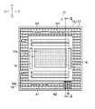
- information about the semiconductor package 10 is described on the surface (more specifically, the upper surface 14a) of the stiffener 14 attached to the package base material 17.
- the information regarding the semiconductor package 10 includes a character image A1 representing the country of manufacture of the semiconductor chip 11, a character image A2 representing the manufacturer of the semiconductor chip 11, a character image A3 representing the model number of the semiconductor chip 11, and a semiconductor.
- the character image A4 representing the unique number of the chip 11 and the code B including the information thereof.
- the "character image” includes characters, symbols, marks, logos, and the like.
- the information included in the code B may be a part of the information represented by the character images A1 to A4.
- the code B preferably contains a unique number of the semiconductor chip 11.
- the manufacturing process of the semiconductor package 10 can be simplified.
- code B and the character images A1 to A4 may be described by the same means.
- the code B and all of the character images A1 to A4 may be described by a laser, or the code B and all of the character images A1 to A4 may be described by ink. By doing so, the manufacturing process of the semiconductor package 10 can be further simplified.
- the part that describes the information about the semiconductor package 10 is not limited to the example shown in FIG. For example, it may be described on the side surface 14b (see FIG. 2) of the stiffener 14, or may be described dispersedly on the upper surface 14a and the side surface 14b.
- the component in which the information regarding the semiconductor package 10 is described does not have to be the stiffener 14.
- information about the semiconductor package 10 may be described on the surface of another electronic component attached to the package base material 17, or a dedicated component containing information about the semiconductor package 10 may be described on the package base material 17. It may be attached.
- explanations, symbols, and marks indicating that the character images A1 to A4 and the code B are information about the semiconductor chip 11 may be described in addition to the character images A1 to A4 and the code B.
- the information about the semiconductor package 10 is described on the surface of another electronic component attached to the package base material 17, the information about the semiconductor package 10 and the information about the electronic component (model number or unique) are included in this component. Information) and may be described.
- the portion for describing the information regarding the semiconductor package 10 may be, for example, the upper surface 17a of the package base material 17.
- the character images A1 to A4 are described on the upper surface 17a of the package base material 17, while the code B containing such information is described on the upper surface 14a of the stiffener 14.
- the information shown on the upper surface 17a of the package base material 17 and the information shown on the upper surface 14a of the stiffener 14 may be described by different means.
- the information shown on the top surface 17a of the package substrate 17 may be described by ink, and the information shown on the top surface 14a of the stiffener 14 may be described by laser. By doing so, the protective layer formed on the surface of the package base material 17 can be well maintained.
- the portion for describing the information regarding the semiconductor package 10 may be dispersedly described on the upper surface 14a of the stiffener 14 and the upper surface 17a of the package base material 17.
- the character image A4 showing the unique information of the semiconductor chip 11 is described in the stretched portion on the left side of the stiffener 14, and the character image A3 showing the code B and the model number is on the upper surface of the stretched portion 14B on the front side of the stiffener 14.
- the stretched portions 14A and 14B are orthogonal to each other.
- the character image A2 representing the manufacturing company and the character image A1 representing the country of manufacture of the semiconductor chip 11 are recorded on the package base material 17.
- the semiconductor package 10 has an insulating portion 15 that covers a conductor element such as a capacitor 16 and a circuit pattern formed on the package base material 17.
- the insulating portion 15 is formed between the inner side surface of the stiffener 14 and the side surface 11b of the semiconductor chip 11 and is filled between them.
- the insulating portion 15 is, for example, a resin. More specifically, the insulating portion 15 is a portion where a liquid or gel-like resin is cured. As the insulating portion 15, for example, an ultraviolet curable resin can be used.
- the insulating portion 15 can prevent the heat conductive material 31 from touching a conductor element such as a capacitor 16 or a circuit pattern.
- the height of the upper surface 16a of the capacitor 16 (height from the upper surface 17a of the substrate 17) is lower than the height of the upper surface 11a of the semiconductor chip 11. It is desirable that the insulating portion 15 covers the upper surface 16a of the capacitor 16. The height of the upper surface 14a of the stiffener 14 (height from the upper surface 17a of the substrate 17) is exposed from the upper surface 15a of the insulating portion 15. As will be described in detail later, the semiconductor package 10 may have a sheet covering the upper surface 16a of the capacitor 16 instead of the insulating portion 15 (see FIG. 6).
- the electronic device 1 has a sealing member 33 that surrounds the heat conductive material 31 in a plan view.
- the sealing member 33 is formed of, for example, a material having cushioning properties. That is, the seal member 33 is made of, for example, a material that allows a change in the thickness of the seal member 33 in the direction in which the upper surface 11a of the semiconductor chip 11 and the lower surface 50c of the radiator 50 face each other, that is, in the vertical direction.
- the material of the sealing member 33 is, for example, rubber, sponge, foamable resin, silicone, or the like.
- the seal member 33 is formed with an opening for exposing the upper surface 11a of the semiconductor chip 11, and the heat conductive material 31 and the semiconductor chip 11 are located inside the seal member 33.
- the sealing member 33 is separated outward from the outer edge (side surface 11b) of the semiconductor chip 11 and is arranged between the semiconductor package 10 and the lower surface 50c of the radiator 50 to seal the gap between them. Thereby, the range in which the heat conductive material 31 having fluidity is scattered can be limited. As a result, as will be described later, it is possible to prevent the heat conductive material 31 from adhering to the character images A1 to A4 and the code B.
- the seal member 33 is arranged inside the stiffener 14.
- the portion where the information about the semiconductor package 10 is described may be located outside the sealing member 33. By doing so, even when the fluidized heat conductive material 31 is scattered inside the sealing member 33, the portion where the information about the semiconductor package 10 is described (for example, the code B or the character images A1 to A4) is covered. The heat conductive material 31 is not attached. Therefore, for example, repair work can be performed efficiently.
- the character images A1 to A4 and the code B are formed on the surface of the stiffener 14.
- the seal member 33 is located inside the stiffener 14. Therefore, the character images A1 to A4 and the code B described on the surface of the stiffener 14 are located outside the seal member 33. As a result, it is possible to effectively prevent the heat conductive material 31 from adhering to the character images A1 to A4 and the code B described on the surface of the stiffener 14.
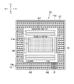
- the character images A1 to A4 representing the information of the semiconductor chip 11 are described on the surface of the package base material 17, and the code B is described on the stiffener 14.
- the insulating portion 15 is formed inside the stiffener 14. Therefore, in the semiconductor package 10 shown in FIG. 3, the cord B is located outside the sealing member 33, and the heat conductive material 31 can be effectively suppressed from adhering to the cord B.
- the character images A1 to A4 described on the package base material 17 are covered with the insulating portion 15.
- the insulating portion 15 is made of a transparent material, the repair worker can read the character images A1 to A4 through the insulating portion 15.
- the character images A3 and A4 representing the model number and the unique information of the semiconductor chip 11 and the code B are described in the stiffener 14, and the character images A1 and A2 representing the country of manufacture and the manufacturing company, respectively. Is described on the surface of the package base material 17 (specifically, the upper surface 17a).
- the code B and the character images A3 and A4 are located on the outside of the seal member 33, and the heat conductive material 31 can be effectively suppressed from adhering to them.
- the character images A1 and A3 described on the package base material 17 are covered with the insulating portion 15.
- the position of the seal member 33 is not limited to the example shown in FIG.
- the insulating portion 15 may be formed only at the position of the capacitor 16, and the sealing member 33 may be located inside the insulating portion 15 and surround the semiconductor chip 11.
- the seal member 33 may be sandwiched in the vertical direction by the upper surface 17a of the package substrate 17 and the lower surface 50c of the radiator 50.
- the semiconductor package 10 exemplified in FIGS. 1, 3 and 4 may be applied to such a structure.
- the cord B shown in FIGS. 1, 3 and 4 is located outside the sealing member 33, and it is possible to prevent the fluidized heat conductive material 31 from adhering to the cord B.
- the character image described in the stiffener 14 (for example, the character images A1 to A4 shown in FIG. 1) is also located outside the seal member 33, thereby preventing the heat conductive material 31 from adhering to the character image. Can be done.
- FIG. 5 is a cross-sectional view showing a modified example of the electronic device 1.
- the position of the seal member 33 may be on the stiffener 14 as shown in FIG.
- the seal member 33 is sandwiched in the vertical direction by the upper surface 14a of the stiffener 14 and the lower surface 50c of the radiator 50.
- the semiconductor package 10 exemplified in FIGS. 1, 3 and 4 may be applied to this structure.
- the cord B formed on the upper surface 14a of the stiffener 14 is located below the seal member 33. That is, the code B is covered with the seal member 33.
- the character image described in the stiffener 14 (for example, the character images A1 to A4 shown in FIG. 1) is also located under the seal member 33, and prevents the heat conductive material 31 from adhering to the character image. be able to.
- the seal member 33 may be attached to the lower surface 50c of the radiator 50.
- the seal member 33 may be adhered to the lower surface 50c of the radiator 50.
- FIG. 6 is a cross-sectional view showing still another modification of the electronic device 1.
- the semiconductor package 10 has an insulating sheet 215 and 225 made of an insulating material as an insulating portion that covers a conductor element such as a capacitor 16 and a circuit pattern.
- the insulating sheet 215 has an upper wall 215b located on the upper side of the capacitor 16 and an inner wall 215c located on the inside of the capacitor 16 (semiconductor chip 11 side).
- the lower edge (attached portion 215h) of the inner wall 215c of the insulating sheet 215 is attached to the package base material 17.
- the insulating sheet 225 is arranged below the insulating sheet 215. The two sheets 215 and 225 overlap.
- the insulating sheet 215 is referred to as an upper sheet, and the insulating sheet 225 is referred to as a lower sheet.
- the lower sheet 225 also has an inner wall 225c inside the capacitor 16 (semiconductor chip 11 side), and its lower edge is It is attached to the package base material 17.
- the material of the upper sheet 215 for example, engineering plastics such as polycarbonate and polyamide can be used.
- An example of the material of the lower sheet 225 is polyethylene terephthalate, and the lower sheet 225 may have flexibility.
- the seal member 33 is sandwiched in the vertical direction by the upper sheet 215 and the lower surface 50c of the radiator 50.
- the sealing member 33 is arranged along the inner edge of the upper wall 215b of the upper sheet 215.
- the sheets 215 and 225 have upper walls 215b and 225b that cover the capacitor 16 and the stiffener 14, respectively.
- the sheets 215 and 225 have outer walls 215d and 225d that descend from the outer edges of the upper walls 215b and 225b and cover the stiffener 14, respectively.
- the outer walls 215d and 225d are not attached to the stiffener 14.
- the sealing member 33 may extend from the inner edge of the upper wall 215b to the upper side of the stiffener 14.
- the semiconductor package 10 shown in FIG. 1 may be applied to the structure shown in FIG. In this case, the character images A1 to A4 and the code B described on the upper surface 14a of the stiffener 14 are covered with the sheets 215 and 225. Therefore, it is possible to prevent the fluidized heat conductive material 31 from adhering to the character images A1 to A4 and the code B.
- the repair worker can properly read the code B with the code reader by peeling off the sheets 215 and 225.
- the semiconductor package 10 shown in FIG. 3 may be applied to the structure shown in FIG.
- the code B described in the stiffener 14 is covered with the sheets 215 and 225.
- the character images A1 to A4 described on the package base material 17 are also covered with the sheets 215 and 225, and the fluidized heat conductive material 31 can be prevented from adhering to the character images A1 to A4.
- the semiconductor package 10 shown in FIG. 4 may be applied to the structure shown in FIG.
- the character images A1 and A3 and the code B described on the upper surface 14a of the stiffener 14 are covered with the sheets 215 and 225.
- the character images A2 and A4 described on the surface of the package base material 17 (specifically, the upper surface 17a) are also covered with the sheets 215 and 225.
- the attached portion 215h is formed at the lower end of the inner wall 215c of the upper sheet 215, and the attached portion 215h is attached to the package base material 17 by the liquid gasket E2.
- the lower sheet 225 is attached to the package base material 17 by, for example, an adhesive tape (tape having an adhesive coated on both sides) or an adhesive.
- the liquid gasket has fluidity at room temperature and is dried or homogenized after a certain period of time after being applied to the joint surface to form an elastic or adhesive thin layer.
- Materials of the liquid gasket include, for example, phenol-based, modified ester-based, silicone-based, acrylic-based and the like.
- the heat conductive material 31 Since the heat conductive material 31 has fluidity, it may come out from between the lower surface 50c of the radiator 50 and the upper surface 11a of the semiconductor chip 11. The leaked heat conductive material 31 adheres to the liquid gasket E2.
- the liquid gasket E2 to which the heat conductive material 31 is attached may scatter and spread to the periphery.
- the lower sheet 225 is arranged below the upper sheet 215 and covers the capacitor 16. This makes it possible to prevent the heat conductive material 31 from scattering toward the conductor element such as the capacitor 16 together with the liquid gasket E2 when the radiator 50 and the upper sheet 215 are removed.
- the number of sheets covering the capacitor 16 and the like may be one.
- the stiffener 14 and the capacitor 16 may be covered only with the insulating sheet 215 or may be covered only with the insulating sheet 225.
- the structure of the sheets 215 and 225 is not limited to the example shown in FIG.
- the sheets 215 and 225 may have an outer wall located between the stiffener 14 and the capacitor 16. That is, the sheets 215 and 225 do not have to cover the stiffener 14.
- the seal member 33 may be sandwiched between the upper surface 14a of the stiffener 14 and the lower surface 50c of the radiator 50, or may be arranged between the sheets 215 and 225 and the radiator 50.
- a semiconductor package 10 having a semiconductor chip 11 and a package base material 17 on which the semiconductor chip 11 is mounted.
- components such as the capacitor 16 may be mounted on the package base material 17.
- the stiffener 14 is attached to the package base material 17, and the above-mentioned insulating portion 15 is formed. Sheets 215 and 225 (FIG. 6) may be attached instead of the insulating portion 15.
- the information regarding the semiconductor package 10 (for example, the unique information of the semiconductor chip 11 described above) is located outside the outer edge 11d of the semiconductor chip 11 instead of the upper surface 11a of the semiconductor chip 11 and is located outside the outer edge of the package base material 17. It is described in the portion located inside 17d.
- information about the semiconductor package 10 is described in the stiffener 14 with a laser, ink, or a seal. Characters, symbols, logos, marks, and codes are not described on the upper surface 11a of the semiconductor chip 11.
- the semiconductor package 10 is mounted on the main board 2 using the BGA 19. Then, the heat conductive material 31 having fluidity is arranged on the upper surface 11a of the semiconductor chip 11 on the upper surface 11a of the semiconductor chip 11. At this time, it is desirable to spread the heat conductive material 31 over the entire upper surface 11a of the semiconductor chip 11. Further, the seal member 33 surrounding the semiconductor chip 11 is attached to the semiconductor package 10 or the radiator 50. Finally, the radiator 50 is placed on the upper surface 11a of the semiconductor chip 11 and thermally connected to each other. Before arranging the radiator 50 on the upper surface 11a of the semiconductor chip 11, the heat conductive material 31 may also be applied to the lower surface 50c of the radiator 50. The above is an example of a method for manufacturing an electronic device.
- FIG. 7 is a plan view showing the semiconductor package 110 as yet another example of the semiconductor package.
- the same elements as those described so far are given the same sign.
- the differences from the semiconductor packages described so far will be mainly described. For matters not described for the semiconductor package 110, the examples described so far may be applied.
- the semiconductor package 110 is not only a semiconductor chip 11 (for example, a silicon die) that functions as a CPU or a GPU as an electronic component mounted on a package base material 17, but also a semiconductor chip 11 (claimed) during operation of the semiconductor package 10. It may have a component (“second portion” of claim) that has a smaller calorific value than the “first portion”) and a lower temperature than the semiconductor chip 11.
- An example of such a component is an electronic component, for example, a semiconductor chip 12 that functions as a RAM (random access memory) or a flash memory.
- the character images A1 to A4 representing the information regarding the semiconductor package 10 and the code B including this information may be described on the surface (upper surface 12a) of the semiconductor chip 12.
- This information may be described by ink, laser, or seal.
- explanations, symbols, and marks indicating that the character images A1 to A4 and the code B are information about the semiconductor chip 11 may be described in addition to the character images A1 to A4 and the code B.
- information about the semiconductor chip 12, such as a manufacturer of the semiconductor chip 12, a model number (product name), a unique number, and the like may be recorded on the upper surface 12a of the semiconductor chip 12.
- the silicon die may be sealed with a resin. Then, the character images A1 to A4 and the code B may be written on the surface of the resin.
- Such a semiconductor chip 12 may be smaller than the semiconductor chip 11.
- the semiconductor chip 12 may have a size larger than half that of the semiconductor chip 11. Unlike this, the semiconductor chip 12 may have a larger size than the semiconductor chip 11.
- the semiconductor package 10 does not have to have the stiffener 14.
- the code B may be described in the stiffener 14, and only the other character images A1 to A4 may be described in the semiconductor chip 12.
- the semiconductor chip 12 may be covered with an insulating insulating portion 15 in the same manner as the capacitor 16 shown in FIG.
- the semiconductor chip 12 may be covered with the capacitor 16 by the insulating sheet 215 (or 225) shown in FIG.
- the repair worker can properly read the code B with the code reader by peeling off the sheets 215 and 225 at the time of repairing the electronic device 1.
- FIG. 8 is a plan view showing the semiconductor package 310 as still another example of the semiconductor package.
- the same elements as those described so far are given the same sign.
- the differences from the semiconductor packages described so far will be mainly described. For matters not described for the semiconductor package 310, the examples described so far may be applied.
- the semiconductor chip 11 has a high temperature region 11A (“first portion” of the claim) and low temperature regions 11B and 11C (claims) in which the temperature is lower than the high temperature region 11A during operation of the semiconductor chip 11. It has a "second part").
- the semiconductor chip 11 may be, for example, a die called a SoC (System on a chip).
- the semiconductor chip 11 may have a processor core, a memory core, and the like. Then, for example, the region of the circuit block in which the processor core is formed may be the high temperature region 11A, and the region of the circuit block in which the memory core is formed may be the low temperature regions 11B / 11C.
- the semiconductor package 310 information about the semiconductor package 10 may be recorded in the low temperature regions 11B and 11C. That is, the character images A1 to A4 and the code B may be described by a laser, ink, a sticker, or the like. Then, the heat conductive material 31 may be arranged on the upper surface 11a of the semiconductor chip 11. Characters, symbols, logos, marks, and codes are not described in the high temperature region 11A of the upper surface 11a of the semiconductor chip 11. In this case, the heat conductive material 31 having fluidity becomes non-uniform on the upper surface 11a of the semiconductor chip 11. For example, in the region where the character image A1 is described and the region of the code B, the heat conductive material 31 may be reduced as compared with the other regions.
- the calorific value of the low temperature regions 11B and 11C is smaller than that of the high temperature regions 11A, even if the amount of the heat conductive material 31 in those regions 11B and 11C is small, the semiconductor chip 11 maintains high cooling performance. can.
- Such low temperature regions 11B and 11C may be provided along the outer peripheral edge of the semiconductor chip 11. That is, when there is a region where the circuit block does not exist on the outer peripheral edge of the semiconductor chip 11 (semiconductor die), information about the semiconductor package 10 may be described in that region.
- the semiconductor package 310 shown in FIG. 8 may be applied to the structure shown in FIG. 2, FIG. 5, and FIG. That is, the insulating portion 15 (see FIGS. 2 and 5) and the sheets 215 and 225 may be attached to the semiconductor package 310. Further, the seal member 33 may be arranged between the semiconductor package 310 and the radiator 50.
- a semiconductor package 310 having a semiconductor chip 11 and a package base material 17 on which the semiconductor chip 11 is mounted.
- components such as the capacitor 16 may be mounted on the package base material 17.
- the stiffener 14 is attached to the package base material 17, and the above-mentioned insulating portion 15 is formed. Sheets 215 and 225 (FIG. 6) may be attached instead of the insulating portion 15. Further, in the semiconductor package 310, the stiffener 14 may not be attached to the package base material 17.
- information about the semiconductor package 10 (for example, the above-mentioned unique information) is described in the low temperature regions 11B and 11C of the upper surface 11a of the semiconductor chip 11. For example, information about the semiconductor package 10 is described in the low temperature regions 11B and 11C by laser, ink, seal, and engraving.
- the semiconductor package 310 is mounted on the main board 2 using BGA19. Then, the heat conductive material 31 having fluidity is arranged on the upper surface 11a of the semiconductor chip 11 on the upper surface 11a of the semiconductor chip 11. At this time, it is desirable to spread the heat conductive material 31 over a wide range of the upper surface 11a of the semiconductor chip 11. Further, the seal member 33 surrounding the semiconductor chip 11 is attached to the semiconductor package 10 or the radiator 50. Finally, the radiator 50 is placed on the upper surface 11a of the semiconductor chip 11 and thermally connected to each other. Before arranging the radiator 50 on the upper surface 11a of the semiconductor chip 11, the heat conductive material 31 may also be applied to the lower surface 50c of the radiator 50. The above is an example of a method for manufacturing an electronic device having a semiconductor package 310.
- FIG. 9 is a cross-sectional view showing a semiconductor package 410 as yet another example of the semiconductor package.
- the same elements as those described so far are given the same sign.
- the differences from the semiconductor packages described so far will be mainly described. For matters not described for the semiconductor package 410, the examples described so far may be applied.
- the semiconductor package 410 has a semiconductor chip 11. Character images A1 to A4 and / or code B indicating information about the semiconductor package 10 are described on the upper surface 11a of the semiconductor chip 11. In the example shown in FIG. 9, the character images A1 to A4 and / or the code B are described by a laser, and the upper surface 11a is slightly recessed in the region where they are described. A surface treatment layer 419 is formed on the upper surface 11a of the semiconductor chip 11 to cover the regions in which the character images A1 to A4 and / or the code B are described. The surface treatment layer 419 may be formed over the entire surface of the upper surface 11a of the semiconductor chip 11.
- the surface treatment layer 419 is applied to the upper surface 11a of the semiconductor chip 11 to eliminate the difference in wettability occurring on the upper surface 11a.
- the flatness of the upper surface 11a may be made uniform.
- the surface treatment layer 419 may be, for example, a coating agent or grease.
- the region (recess) in which the character images A1 to A4 and / or the code B are described is filled with the surface treatment layer 419, and the surface treatment layer 419 has a flat and uniform wettability upper surface.
- the heat conductive material 31 described above is arranged between the surface treatment layer 419 and the radiator 50.
- the wettability of the heat conductive material 31 having fluidity becomes uniform, and the non-uniformity of the thickness of the heat conductive material 31 can be reduced.
- the upper surface of the surface treatment layer 419 does not necessarily have to be flat.
- the information (character images A1 to A4 and / or the code B) regarding the semiconductor package 10 may be described by ink, a sticker, or an engraving instead of the laser.
- the thickness of the surface treatment layer 419 may be thin in the area where the ink or the seal is present, and may be relatively thick in the other areas. By doing so, the surface treatment layer 419 may have a flat upper surface.
- the surface treatment layer 419 is preferably thinner than the heat conductive material 31. By doing so, the thermal resistance of the surface treatment layer 419 can be reduced.
- the thickness of the surface treatment layer 419 may be smaller than half the thickness of the heat conductive material 31.
- the regions where the character images A1 to A4 and / or the code B showing the information about the semiconductor package 10 are formed may be the low temperature regions 11B and 11C described with reference to FIG. By doing so, the high cooling performance of the semiconductor chip 11 can be maintained more effectively.
- the semiconductor package 410 shown in FIG. 9 may be applied to the structure shown in FIG. 2, FIG. 5, and FIG. That is, the insulating portion 15 (see FIGS. 2 and 5) may be formed on the semiconductor package 410, or the sheets 215 and 225 may be attached. Further, the seal member 33 may be arranged between the semiconductor package 410 and the radiator 50.
- a semiconductor package 410 having a semiconductor chip 11 and a package base material 17 on which the semiconductor chip 11 is mounted.
- components such as the capacitor 16 may be mounted on the package base material 17.
- the stiffener 14 is attached to the package base material 17, and the above-mentioned insulating portion 15 is formed. Sheets 215 and 225 (FIG. 6) may be attached instead of the insulating portion 15. Further, in the semiconductor package 410, the stiffener 14 may not be attached to the package base material 17.
- information about the semiconductor package 10 (for example, the above-mentioned unique information) is described on the upper surface 11a of the semiconductor chip 11. For example, information about the semiconductor package 10 is described on the upper surface 11a of the semiconductor chip 11 with a laser, ink, or a seal.
- BGA19 is used to mount the semiconductor package 410 on the main board 2 (see FIG. 2). Further, grease is applied or a coating agent is formed on the upper surface 11a of the semiconductor chip 11 to form the surface treatment layer 419. At this time, the area in which the information regarding the semiconductor package 10 is described is covered with the surface treatment layer 419. Next, the heat conductive material 31 is arranged on the surface treatment layer 419. At this time, it is desirable to spread the heat conductive material 31 over the entire upper surface 11a of the semiconductor chip 11. Further, the seal member 33 surrounding the semiconductor chip 11 is attached to the semiconductor package 10 or the radiator 50. Finally, the radiator 50 is placed on the upper surface 11a of the semiconductor chip 11 and thermally connected to each other. Before arranging the radiator 50 on the upper surface 11a of the semiconductor chip 11, the heat conductive material 31 may also be applied to the lower surface 50c of the radiator 50. The above is an example of a method for manufacturing an electronic device having a semiconductor package 410.
- the information about the semiconductor package 10 is not the surface (upper surface 11a) of the semiconductor chip 11 but the outer edge 11d of the semiconductor chip 11. Described on a portion located on the outside and inside the outer edge 17d of the package base material 17 (the stiffener 14, the surface of the package base material 17 (specifically, the upper surface 17a), and other electronic components 12). ing. Then, a heat conductive material 31 having fluidity is arranged between the upper surface 11a of the semiconductor chip 11 and the radiator 50. According to this, the flatness of the upper surface 11a of the semiconductor chip 11 is maintained, and the heat conductive material having fluidity spreads uniformly on the upper surface 11a of the semiconductor chip 11, so that high cooling performance can be obtained for the semiconductor chip 11.
- the semiconductor chip 11 has a high temperature region 11A and low temperature regions 11B and 11C whose temperature is lower than that of the high temperature region 11A when the semiconductor chip 11 operates. ing. Information about the semiconductor package 10 is described in the low temperature regions 11B and 11C instead of the high temperature regions 11A of the semiconductor chip 11.
- a heat conductive material 31 having fluidity is arranged between the upper surface 11a of the semiconductor chip 11 and the radiator 50. Since the calorific value of the low temperature regions 11B and 11C is smaller than that of the high temperature regions 11A, even if the amount of the heat conductive material 31 in those regions 11B and 11C is small, the semiconductor chip 11 maintains high cooling performance. can.
- the upper surface 11a of the semiconductor chip 11 has a region in which information about the semiconductor package 10 is described.
- a surface treatment layer 419 covering the region in which this information is described is formed on the upper surface 11a of the semiconductor chip 11, and a heat conductive material 31 having fluidity is arranged between the surface treatment layer 419 and the radiator 50. ing. According to this, since the flat surface is formed by the surface treatment layer 419, the heat conductive material 31 can be uniformly arranged between the surface treatment layer 419 and the radiator 50.
- the structure proposed in the present disclosure may be applied to, for example, a semiconductor package having a plurality of stacked semiconductor chips (silicon dies). Even in this case, the following structures (1) to (3) may be adopted.
- Information about this semiconductor chip may be described not in the upper surface of the semiconductor chip at the uppermost portion but in the outer portion (component) of the outer edge of the upper surface of the semiconductor chip.
- a high temperature region and a low temperature region may be specified on the upper surface of the semiconductor chip located at the uppermost portion, and information about the semiconductor chip may be described in the low temperature region.
- An area in which information about the semiconductor chip is described may be secured on the upper surface of the semiconductor chip located at the uppermost portion. Then, this region may be covered with a surface treatment layer, and a heat conductive material having fluidity may be arranged on the upper side of the surface treatment layer.
Landscapes
- Cooling Or The Like Of Semiconductors Or Solid State Devices (AREA)
- Chemical & Material Sciences (AREA)
- Engineering & Computer Science (AREA)
- Materials Engineering (AREA)
Priority Applications (4)
| Application Number | Priority Date | Filing Date | Title |
|---|---|---|---|
| US18/044,847 US20230298963A1 (en) | 2020-09-24 | 2021-09-17 | Semiconductor package, electronic device, and electronic device manufacturing method |
| EP21872386.4A EP4220703A4 (en) | 2020-09-24 | 2021-09-17 | SEMICONDUCTOR PACKAGE, ELECTRONIC EQUIPMENT AND METHOD FOR MANUFACTURING ELECTRONIC EQUIPMENT |
| CN202180058888.2A CN116157913A (zh) | 2020-09-24 | 2021-09-17 | 半导体封装、电子设备和电子设备制造方法 |
| JP2022551967A JP7504214B2 (ja) | 2020-09-24 | 2021-09-17 | 半導体パッケージ、電子機器、及び電子機器の製造方法 |
Applications Claiming Priority (2)
| Application Number | Priority Date | Filing Date | Title |
|---|---|---|---|
| JP2020-159895 | 2020-09-24 | ||
| JP2020159895 | 2020-09-24 |
Publications (1)
| Publication Number | Publication Date |
|---|---|
| WO2022065257A1 true WO2022065257A1 (ja) | 2022-03-31 |
Family
ID=80845377
Family Applications (1)
| Application Number | Title | Priority Date | Filing Date |
|---|---|---|---|
| PCT/JP2021/034411 Ceased WO2022065257A1 (ja) | 2020-09-24 | 2021-09-17 | 半導体パッケージ、電子機器、及び電子機器の製造方法 |
Country Status (6)
| Country | Link |
|---|---|
| US (1) | US20230298963A1 (https=) |
| EP (1) | EP4220703A4 (https=) |
| JP (1) | JP7504214B2 (https=) |
| CN (1) | CN116157913A (https=) |
| TW (1) | TW202220064A (https=) |
| WO (1) | WO2022065257A1 (https=) |
Families Citing this family (1)
| Publication number | Priority date | Publication date | Assignee | Title |
|---|---|---|---|---|
| TWI879409B (zh) * | 2024-01-30 | 2025-04-01 | 矽品精密工業股份有限公司 | 半導體封裝結構及其製法 |
Citations (7)
| Publication number | Priority date | Publication date | Assignee | Title |
|---|---|---|---|---|
| JP2002016102A (ja) * | 2000-06-28 | 2002-01-18 | Seiko Epson Corp | 半導体装置及びその製造方法、回路基板並びに電子機器 |
| JP2007335742A (ja) | 2006-06-16 | 2007-12-27 | Sony Computer Entertainment Inc | 半導体装置およびその製造方法 |
| JP2009194321A (ja) * | 2008-02-18 | 2009-08-27 | Shinko Electric Ind Co Ltd | 配線基板及びその製造方法、半導体パッケージ |
| JP2012069902A (ja) | 2010-08-27 | 2012-04-05 | Sony Corp | 放熱構造及び電子機器 |
| US20160172306A1 (en) * | 2014-12-16 | 2016-06-16 | Deca Technologies Inc. | Method of marking a semiconductor package |
| JP2016192444A (ja) * | 2015-03-30 | 2016-11-10 | 株式会社東芝 | 半導体装置 |
| WO2020162417A1 (ja) | 2019-02-04 | 2020-08-13 | 株式会社ソニー・インタラクティブエンタテインメント | 電子機器、半導体装置、絶縁シート、及び半導体装置の製造方法 |
Family Cites Families (13)
| Publication number | Priority date | Publication date | Assignee | Title |
|---|---|---|---|---|
| US4594263A (en) * | 1984-12-17 | 1986-06-10 | Motorola, Inc. | Laser marking method and ablative coating for use therein |
| JPH01216558A (ja) * | 1988-02-24 | 1989-08-30 | Hitachi Ltd | 半導体装置 |
| JP3437369B2 (ja) * | 1996-03-19 | 2003-08-18 | 松下電器産業株式会社 | チップキャリアおよびこれを用いた半導体装置 |
| US6984876B2 (en) * | 2004-05-27 | 2006-01-10 | Semiconductor Components Industries, L.L.C. | Semiconductor device formed having a metal layer for conducting the device current and for high contrast marking and method thereof |
| US7667949B2 (en) * | 2006-08-05 | 2010-02-23 | John Maxwell | Capacitor having improved surface breakdown voltage performance and method for marking same |
| US7489033B2 (en) * | 2006-11-10 | 2009-02-10 | Intel Corporation | Electronic assembly with hot spot cooling |
| JP5184003B2 (ja) * | 2007-08-28 | 2013-04-17 | 川崎マイクロエレクトロニクス株式会社 | 半導体集積回路およびダミーパターンの配置方法 |
| US8187897B2 (en) * | 2008-08-19 | 2012-05-29 | International Business Machines Corporation | Fabricating product chips and die with a feature pattern that contains information relating to the product chip |
| US8522569B2 (en) * | 2009-10-27 | 2013-09-03 | Industrial Idea Partners, Inc. | Utilization of data center waste heat for heat driven engine |
| US20110259951A1 (en) * | 2010-04-26 | 2011-10-27 | Medtronic, Inc. | Method for Tracing Individual Dies |
| US9589900B2 (en) * | 2014-02-27 | 2017-03-07 | Taiwan Semiconductor Manufacturing Company, Ltd. | Metal pad for laser marking |
| US9832860B2 (en) * | 2014-09-26 | 2017-11-28 | Intel Corporation | Panel level fabrication of package substrates with integrated stiffeners |
| EP3227399B1 (en) * | 2014-12-05 | 2021-07-14 | Honeywell International Inc. | High performance thermal interface materials with low thermal impedance |
-
2021
- 2021-09-16 TW TW110134544A patent/TW202220064A/zh unknown
- 2021-09-17 JP JP2022551967A patent/JP7504214B2/ja active Active
- 2021-09-17 CN CN202180058888.2A patent/CN116157913A/zh active Pending
- 2021-09-17 EP EP21872386.4A patent/EP4220703A4/en active Pending
- 2021-09-17 WO PCT/JP2021/034411 patent/WO2022065257A1/ja not_active Ceased
- 2021-09-17 US US18/044,847 patent/US20230298963A1/en active Pending
Patent Citations (7)
| Publication number | Priority date | Publication date | Assignee | Title |
|---|---|---|---|---|
| JP2002016102A (ja) * | 2000-06-28 | 2002-01-18 | Seiko Epson Corp | 半導体装置及びその製造方法、回路基板並びに電子機器 |
| JP2007335742A (ja) | 2006-06-16 | 2007-12-27 | Sony Computer Entertainment Inc | 半導体装置およびその製造方法 |
| JP2009194321A (ja) * | 2008-02-18 | 2009-08-27 | Shinko Electric Ind Co Ltd | 配線基板及びその製造方法、半導体パッケージ |
| JP2012069902A (ja) | 2010-08-27 | 2012-04-05 | Sony Corp | 放熱構造及び電子機器 |
| US20160172306A1 (en) * | 2014-12-16 | 2016-06-16 | Deca Technologies Inc. | Method of marking a semiconductor package |
| JP2016192444A (ja) * | 2015-03-30 | 2016-11-10 | 株式会社東芝 | 半導体装置 |
| WO2020162417A1 (ja) | 2019-02-04 | 2020-08-13 | 株式会社ソニー・インタラクティブエンタテインメント | 電子機器、半導体装置、絶縁シート、及び半導体装置の製造方法 |
Also Published As
| Publication number | Publication date |
|---|---|
| TW202220064A (zh) | 2022-05-16 |
| JP7504214B2 (ja) | 2024-06-21 |
| JPWO2022065257A1 (https=) | 2022-03-31 |
| EP4220703A4 (en) | 2025-01-08 |
| EP4220703A1 (en) | 2023-08-02 |
| US20230298963A1 (en) | 2023-09-21 |
| CN116157913A (zh) | 2023-05-23 |
Similar Documents
| Publication | Publication Date | Title |
|---|---|---|
| JP7311540B2 (ja) | 電子機器、半導体装置、絶縁シート、及び半導体装置の製造方法 | |
| JP5983032B2 (ja) | 半導体パッケージ及び配線基板ユニット | |
| JP5899768B2 (ja) | 半導体パッケージ、配線基板ユニット、及び電子機器 | |
| US7704798B2 (en) | Electronic assemblies with hot spot cooling and methods relating thereto | |
| JP5096782B2 (ja) | 半導体装置 | |
| US10424527B2 (en) | Electronic package with tapered pedestal | |
| WO2011121779A1 (ja) | マルチチップモジュール、プリント配線基板ユニット、マルチチップモジュールの製造方法およびプリント配線基板ユニットの製造方法 | |
| US12278150B2 (en) | Semiconductor package with annular package lid structure | |
| CN215266269U (zh) | 一种电路板组件、散热器和电子设备 | |
| TWI658549B (zh) | 散熱型封裝結構 | |
| US20220199429A1 (en) | Structural thermal interfacing for lidded semiconductor packages | |
| JP7504214B2 (ja) | 半導体パッケージ、電子機器、及び電子機器の製造方法 | |
| JPWO2022065257A5 (https=) | ||
| CN116936497A (zh) | 应用于集成电路的冷却封装结构及其组装方法 | |
| US20240243114A1 (en) | Electronic package structure | |
| EP4456128A1 (en) | Thermal management systems and methods for semiconductor devices | |
| TWI438878B (zh) | 半導體裝置及製造具有改良的散熱能力的半導體裝置之方法 | |
| JP7152544B2 (ja) | 半導体放熱パッケージ構造 | |
| TWI624217B (zh) | 熱擴散式電子裝置 | |
| US10665524B2 (en) | Electronic package cover having underside rib | |
| US20240055417A1 (en) | Electronic package structure | |
| Hirasawa et al. | Evolution of the heatsink technology | |
| CN121171992A (zh) | 芯片封装结构、电子设备以及制备方法 | |
| CN116564908A (zh) | 散热构造以及电子设备 | |
| CN119092417A (zh) | 一种半导体封装结构及制作方法 |
Legal Events
| Date | Code | Title | Description |
|---|---|---|---|
| 121 | Ep: the epo has been informed by wipo that ep was designated in this application |
Ref document number: 21872386 Country of ref document: EP Kind code of ref document: A1 |
|
| ENP | Entry into the national phase |
Ref document number: 2022551967 Country of ref document: JP Kind code of ref document: A |
|
| NENP | Non-entry into the national phase |
Ref country code: DE |
|
| ENP | Entry into the national phase |
Ref document number: 2021872386 Country of ref document: EP Effective date: 20230424 |