WO2022065161A1 - 透明導電膜基材およびセンサ装置 - Google Patents
透明導電膜基材およびセンサ装置 Download PDFInfo
- Publication number
- WO2022065161A1 WO2022065161A1 PCT/JP2021/033954 JP2021033954W WO2022065161A1 WO 2022065161 A1 WO2022065161 A1 WO 2022065161A1 JP 2021033954 W JP2021033954 W JP 2021033954W WO 2022065161 A1 WO2022065161 A1 WO 2022065161A1
- Authority
- WO
- WIPO (PCT)
- Prior art keywords
- conductive film
- transparent conductive
- insulating layer
- line width
- substrate
- Prior art date
- Legal status (The legal status is an assumption and is not a legal conclusion. Google has not performed a legal analysis and makes no representation as to the accuracy of the status listed.)
- Ceased
Links
Images



Classifications
-
- B—PERFORMING OPERATIONS; TRANSPORTING
- B32—LAYERED PRODUCTS
- B32B—LAYERED PRODUCTS, i.e. PRODUCTS BUILT-UP OF STRATA OF FLAT OR NON-FLAT, e.g. CELLULAR OR HONEYCOMB, FORM
- B32B7/00—Layered products characterised by the relation between layers; Layered products characterised by the relative orientation of features between layers, or by the relative values of a measurable parameter between layers, i.e. products comprising layers having different physical, chemical or physicochemical properties; Layered products characterised by the interconnection of layers
- B32B7/02—Physical, chemical or physicochemical properties
- B32B7/025—Electric or magnetic properties
-
- H—ELECTRICITY
- H01—ELECTRIC ELEMENTS
- H01B—CABLES; CONDUCTORS; INSULATORS; SELECTION OF MATERIALS FOR THEIR CONDUCTIVE, INSULATING OR DIELECTRIC PROPERTIES
- H01B5/00—Non-insulated conductors or conductive bodies characterised by their form
- H01B5/14—Non-insulated conductors or conductive bodies characterised by their form comprising conductive layers or films on insulating-supports
-
- H—ELECTRICITY
- H01—ELECTRIC ELEMENTS
- H01Q—ANTENNAS, i.e. RADIO AERIALS
- H01Q1/00—Details of, or arrangements associated with, antennas
- H01Q1/42—Housings not intimately mechanically associated with radiating elements, e.g. radome
-
- H—ELECTRICITY
- H05—ELECTRIC TECHNIQUES NOT OTHERWISE PROVIDED FOR
- H05K—PRINTED CIRCUITS; CASINGS OR CONSTRUCTIONAL DETAILS OF ELECTRIC APPARATUS; MANUFACTURE OF ASSEMBLAGES OF ELECTRICAL COMPONENTS
- H05K9/00—Screening of apparatus or components against electric or magnetic fields
Definitions
- the present invention relates to a transparent conductive film substrate used as an electromagnetic shield.
- the present invention also relates to a sensor device using a transparent conductive film substrate.
- the sensor is mounted on an automobile, for example, and is used for measuring the inter-vehicle distance and the relative speed between the vehicle in front of the vehicle and its own vehicle.
- Such a sensor is a transparent conductive film that functions as an electromagnetic shield in order to shield radio waves coming from the outside and improve the signal-to-noise ratio (S / N ratio) of the sensor. Often covered by a substrate. Further, when the sensor is mounted on an automobile, it is known that snow accretion and icing on the automobile cause communication failure in the sensor. Therefore, in order to melt the snow and ice adhering to the automobile, the transparent conductive film base material often has a function as a heater.
- Patent Document 1 discloses a radar cover having a wiring pattern made of fine metal wires formed by copper plating or etching, transmitting electromagnetic waves transmitted and received by a sensor, and functioning as a heater. ing.
- Patent Document 1 when the fine metal wire is formed by plating or etching, scattered reflection of visible light is likely to occur in the fine metal wire, and the fine metal wire is conspicuously visually recognized. There was a problem that visibility was difficult. Further, in the metal thin wire as disclosed in Patent Document 1, scattered reflection is likely to occur even for electromagnetic waves in a wavelength range other than the wavelength region of visible light, and a transparent conductive film base material is arranged in the vicinity of the sensor. In this case, there is a problem that the signal detected by the sensor tends to include noise caused by scattered and reflected electromagnetic waves.
- a technique of forming a fine metal wire by plating a patterned resin is also known.
- this technology to form a thin conductive film on the resin, it is possible to suppress the scattering and reflection of electromagnetic waves caused by the metal layer, but the sensor detects by blocking the radio waves coming from the outside.
- the thickness of the metal layer it is necessary to make the thickness of the metal layer more than a certain level and lower the resistance value of the thin metal wire to some extent.
- the line width of the metal layer becomes wider than the line width of the resin layer, and the portion of the metal layer protruding from the resin layer is the surface of the substrate on which the fine metal wire is formed.
- the signal detected by the sensor on the opposite side was the cause of noise.
- the present invention has been made to solve the above problems, and an object of the present invention is to provide a transparent conductive film substrate and a sensor device capable of suppressing the generation of noise while improving visibility.
- the transparent conductive film substrate comprises a substrate having a first surface and a second surface forming the front and back surfaces, and a conductive film formed on at least the first surface of the substrate. It has a scattering reflectance of less than 5% for electromagnetic waves in the wavelength range of 380 nm to 800 nm incident from the first surface side, and has a scattering reflectance in the wavelength range of 1050 nm to 1070 nm incident from the first surface side.
- the conductive film has a film thickness of 2.00 ⁇ m or more.
- a conductive film can be formed on the first surface and the second surface of the substrate.
- the conductive film preferably has a sheet resistance of 0.10 ⁇ / ⁇ or more and 10.00 ⁇ / ⁇ or less.
- the transparent conductive film substrate preferably has a three-dimensional shape.
- the conductive film preferably has a mesh shape formed by a plurality of fine metal wires.
- the thin metal wire preferably has a line width of 20.00 ⁇ m or less.
- the thin metal wire preferably includes an insulating layer formed on the substrate and a metal layer formed on the insulating layer so as to cover the insulating layer.
- the line width of the metal layer in the thin metal wire is W1 and the line width of the insulating layer in the thin metal wire is W2
- the width of the portion of the metal layer existing outside the end of the insulating layer in the line width direction of the thin metal wire It is preferable that (W1-W2) / 2 satisfies (W1-W2) / 2 ⁇ 3.00 ⁇ m and (W1-W2) / 2 ⁇ (W1) / 4.
- the insulating layer has a lower bottom portion in contact with the substrate, an upper bottom portion having a line width narrower than the line width of the lower bottom portion and located at the center portion in the line width direction of the insulating layer, and both ends in the line width direction. It is preferable that the thickness is thinner than the thickness between the upper bottom portion and the lower bottom portion. In this case, it is preferable that the insulating layer has a shape in which the thickness gradually decreases from both ends of the upper bottom portion to both ends of the lower bottom portion in the line width direction.
- the insulating layer contains a resin as a main component.
- the insulating layer preferably contains a polymer having an interacting group that interacts with the plating catalyst. Further, the polymer having an interacting group preferably has a three-dimensional network structure in the insulating layer.
- the metal layer preferably contains any one of copper, silver and aluminum as a main component.
- the substrate preferably contains any one of a polycarbonate resin, a polymethyl methacrylate resin, an acrylonitrile butadiene styrene resin and a polyethylene terephthalate resin as a main component.
- the transparent conductive film substrate preferably has a visible light transmittance of 75.0% or more.
- the sensor device of the present invention includes the above-mentioned transparent conductive film substrate and a sensor that irradiates an electromagnetic wave, and the transparent conductive film substrate is installed with respect to the sensor in the irradiation direction of the electromagnetic wave emitted by the sensor. It is characterized by that.
- the transparent conductive base material is arranged so that the second surface faces the sensor.
- a first surface having a conductive film and a second surface forming the front and back surfaces are formed, and a wavelength range of 380 nm to 800 nm incident from the first surface side is formed. It has a scattering reflectance of less than 5% with respect to the electromagnetic wave of the above, and has a scattering reflectance A of less than 5% with respect to an electromagnetic wave in the wavelength range of 1050 nm to 1070 nm incident from the first surface side, and has a scattering reflectance A.
- the scattering reflectance B for electromagnetic waves in the wavelength range of 1050 nm to 1070 nm incident from the second surface side satisfies the relationship of A / B> 4.0, and the conductive film has a film thickness of 2.00 ⁇ m or more. Therefore, it is possible to suppress the generation of noise while improving the visibility.
- FIG. 1 It is a schematic perspective view of the transparent conductive film base material which concerns on embodiment of this invention. It is sectional drawing which shows a part of the transparent conductive film base material which concerns on embodiment of this invention schematically. It is a schematic diagram which enlarged and shows a part of the conductive film of the transparent conductive film base material which concerns on embodiment of this invention. It is an enlarged sectional view of the conductive film in embodiment of this invention. It is an enlarged sectional view of the conductive film formed by the prior art. It is a figure which shows typically the sensor device in embodiment of this invention.
- the term "transparent to visible light” means that the visible light transmittance is 40% or more in the visible light wavelength range of 380 nm to 800 nm, preferably 80.0% or more. More preferably, it is 90.0% or more. Further, in the following description, transparency means that it is transparent to visible light unless otherwise specified. Visible light transmittance is measured using "Plastic-How to determine total light transmittance and total light reflectance” specified in JIS (Japanese Industrial Standards) K 7375: 2008.
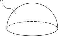
- FIG. 1 shows a transparent conductive film base material 11 according to an embodiment of the present invention.
- the transparent conductive film base material 11 is a film-like base material and has a three-dimensional shape (three-dimensional shape) along a curved surface of a hemisphere.
- the transparent conductive film base material 11 has a three-dimensional shape along a curved surface of a hemisphere, and has an insulating transparent substrate 12 having a first surface 12A and a second surface 12B forming front and back surfaces.
- the conductive film 13 formed on the first surface 12A of the substrate 12 is provided.
- the first surface 12A of the substrate 12 is a surface facing the outside of the hemisphere, and the second surface 12B is a surface facing the inside of the hemisphere.
- the conductive film 13 has a mesh shape and transmits visible light.
- the conductive film 13 has a visible light transmittance of 75.0% or more. Therefore, the transparent conductive film base material 11 also transmits visible light.
- the conductive film 13 is composed of a metal mesh M composed of a metal thin wire 14 having a line width W and having a plurality of square openings 15.
- the thin metal wires 14 parallel to each other and adjacent to each other are arranged so as to be separated by a pitch P defined as a distance between the virtual center lines CL of the thin metal wires 14.
- the line width W of the thin metal wire 14 is not particularly limited, but the upper limit is preferably 1000.00 ⁇ m or less, more preferably 500.00 ⁇ m or less, and even more preferably 300.00 ⁇ m or less.
- the lower limit of the line width W is preferably 2.00 ⁇ m or more, more preferably 5.00 ⁇ m or more. When the line width W is within the above range, the metal mesh M can have high conductivity.
- the thickness of the thin metal wire 14 can be set to 0.01 ⁇ m or more and 200.00 ⁇ m or less, but the upper limit thereof is preferably 30.00 ⁇ m or less, more preferably 20.00 ⁇ m or less, and 9 It is more preferably 0.00 ⁇ m or less, and particularly preferably 3.00 ⁇ m or less.
- the lower limit of the thickness of the thin metal wire 14 is preferably 0.01 ⁇ m or more, more preferably 0.05 ⁇ m or more.
- the sheet resistance of the conductive film 13 is preferably 0.10 ⁇ / ⁇ or more and 10.00 ⁇ / ⁇ or less. As described above, since the conductive film 13 has a sufficiently low sheet resistance, it has a high reflection performance against so-called radio waves. Further, since the conductive film 13 has a resistance value of 0.10 ⁇ / ⁇ or more, heat is generated when the conductive film 13 is energized, and the function of a so-called heater is exhibited. Therefore, the transparent conductive film base material 11 can be used as a so-called electromagnetic shield / heater.
- the upper limit of P is preferably 800.00 ⁇ m or less, more preferably 600.00 ⁇ m or less, still more preferably 400.00 ⁇ m or less.
- the lower limit of the pitch P is preferably 5.00 ⁇ m or more, more preferably 30.00 ⁇ m or more, and even more preferably 80.00 ⁇ m or more.
- the aperture ratio of the metal mesh M is preferably 85% or more, and more preferably 90% or more. , 95% or more is more preferable.
- the aperture ratio of the metal mesh M is the ratio of the transparent portion of the region occupied by the metal mesh M excluding the metal fine wire 14, that is, a plurality of openings with respect to the entire area of the metal mesh M. It corresponds to the ratio of the total area occupied by 15.
- the shape of the plurality of openings 15 of the metal mesh M is not limited to a square, and is, for example, a triangle such as a regular triangle, an isosceles triangle, a right triangle, a square, a rectangle, a parallelogram, a quadrangle such as a trapezoid, ( It can also be a geometric figure that combines (regular) polygons such as (regular) hexagons and (regular) octagons, circles, ellipses, and stars.
- the transparent conductive film base material 11 can be used for electromagnetic waves in the wavelength range of 380 nm to 800 nm (visible light) and electromagnetic waves in the wavelength range of 1050 nm to 1070 nm (infrared light) incident from the first surface 12A side of the substrate 12.
- it has a scattering reflectance of less than 5.0%, preferably a scattering reflectance of 2.5% or less, and more preferably 2.0% or less.
- the lower limit of the scattering reflectance is not particularly limited, and examples thereof include 0.0%.
- the scattered reflectance is a value that can be calculated by subtracting the specular reflectance from the total reflectance (measured value of all angles of the integrating sphere).
- FIG. 4 shows a cross-sectional view of the thin metal wire 14 when the thin metal wire 14 is cut in the line width direction and the cross section is viewed from the front.
- the thin metal wire 14 forming the conductive film 13 includes an insulating layer 16 formed on the first surface 12A of the substrate 12, a metal layer 17 formed on the insulating layer 16, and a metal layer. It has a blackening layer 18 formed on the 17.
- the blackening layer 18 is formed on the metal layer 17 and is for suppressing the visible light emitted from the first surface 12A side of the substrate 12 from being reflected on the metal layer 17. As a result, when the observer sees the transparent conductive film base material 11 from the first surface 12A side, the thin metal wire 14 is prevented from being conspicuously visually recognized, and the visibility from the first surface 12A side is improved. ..
- the blackening layer 18 for example, metal oxide, metal nitride, metal oxynitride, metal sulfide and the like are used, and typically, copper oxynitride, copper nitride, copper oxide, molybdenum oxide and the like are used. can.
- the insulating layer 16 is formed of a material containing an insulating resin as a main component. More specifically, it is preferable that the insulating layer 16 contains a polymer having a functional group (interactive group) that interacts with the plating catalyst, and the polymer forms a three-dimensional network structure.
- the insulating layer 16 has a lower bottom portion 16A that is in contact with the first surface 12A of the substrate 12 and has a line width W2, and an upper line width that is narrower than the line width W2 of the lower bottom portion 16A in the line width direction of the thin metal wire 14. It has a bottom portion 16B, and has a trapezoidal cross-sectional shape in which the thickness gradually decreases from both ends of the upper bottom portion 16B to both ends of the lower bottom portion 16A in the line width direction.
- the line width of the insulating layer 16 is defined by the line width of the lower bottom portion 16A.
- the metal layer 17 is formed on the insulating layer 16, it has a line width W1 wider than the line width W2 of the insulating layer 16 in the line width direction, and protrudes from both ends of the insulating layer 16.
- the line width W1 of the metal layer 17 defines the line width of the thin metal wire 14.
- the metal layer 17 is formed by immersing the insulating layer 16 in a so-called plating solution and precipitating metal on the insulating layer 16.
- the metal forming the metal layer 17 the more the abundance of the plating catalyst is, the larger the precipitation amount is, and the less the abundance of the plating catalyst is, the smaller the precipitation amount is. Therefore, the thickness of the metal layer 17 is the thickest on the upper bottom portion 16B, which is the portion where the insulating layer 16 is the thickest, and therefore the portion containing the most interacting groups that interact with the plating catalyst, and both ends of the upper bottom portion 18B. It gradually becomes thinner from the portion to both ends of the lower bottom portion 18A.
- both ends of the insulating layer 16 in the line width direction have a shape that rises from the first surface 12A of the substrate 12 so as to form an acute angle. There is. Therefore, it is possible to prevent the metal from protruding from both ends of the insulating layer 16 in the line width direction and precipitating.
- the metal layer 17 is suppressed from protruding from the insulating layer 16 in the line width direction of the thin metal wire 14, the electromagnetic wave incident from the second surface 12B side of the substrate 12 is caused by the metal layer 17 from the insulating layer 16. Diffuse reflection is suppressed at the protruding portion.
- the scattering reflectance B of the conductive film base material 11 satisfies the relationship of A / B> 4.0.
- the A / B is preferably 5.0 or more.
- the upper limit of A / B is not particularly limited, but is preferably 30.0 or less.
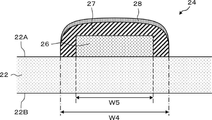
- the thin metal wire 24 formed on the substrate 22 by the conventional technique includes an insulating layer 26 having a substantially rectangular cross-sectional shape, and a metal layer 27 formed on the insulating layer 26. It often has a blackened layer 28 formed on the metal layer 27.
- the insulating layer 26 has a line width W4
- the metal layer 27 has a line width W5
- the metal layer 27 protrudes from both ends of the insulating layer 26.
- the insulating layer 26 has a substantially rectangular cross-sectional shape, the amount of metal deposited on the wall surfaces of both ends of the insulating layer 26 in the line width direction of the thin metal wire 24 is large, and the thin metal wire 24 is formed.
- the width (W4-W5) / 2 of the portion of the metal layer 27 existing outside the one-sided end of the insulating layer 26 is widened.
- the visibility on the first surface 22A side of the substrate 22 can be ensured by the presence of the blackening layer 28, but the observer sees the transparent conductive film base material having the metal thin wire 24 from the second surface 22B side of the substrate 22.
- the portion of the metal layer 27 protruding from the insulating layer 26 is conspicuous because it reflects visible light in the line width direction of the thin metal wire 24, and the visibility on the second surface 22B side is lowered. ..
- an electromagnetic wave is incident from the second surface 22B side of the substrate 22, the electromagnetic wave is likely to be scattered and reflected at a portion where the metal layer 27 protrudes from the insulating layer 26 in the line width direction of the thin metal wire 24, for example.
- a sensor that irradiates and detects electromagnetic waves is arranged on the second surface 22B side of the substrate 22, there is a problem that the signal detected by the sensor tends to include noise caused by scattered and reflected electromagnetic waves. ..
- the metal layer 17 is suppressed from protruding from the insulating layer 16 in the line width direction of the thin metal wire 14. Therefore, when the transparent conductive film base material 11 is observed from the second surface 12B side of the substrate 12, the observer suppresses the reflection of visible light on the portion where the metal layer 17 protrudes from the insulating layer 16. It is suppressed that the thin metal wire 14 is conspicuously visually recognized.
- a sensor device 19 in which the sensor A1 is arranged at a position facing the second surface 12B of the substrate 12 can be configured.
- the sensor A1 in the sensor device 19 can irradiate and detect electromagnetic waves in a wavelength range of, for example, 1050 nm to 1070 nm.
- the transparent conductive film base material 11 since the scattering reflection of the electromagnetic wave incident from the second surface 12B side of the substrate 12 is suppressed, the portion where the metal layer 17 protrudes from the insulating layer 16 in the signal detected by the sensor A1. It is possible to suppress the inclusion of noise caused by electromagnetic waves scattered and reflected by.
- the transparent conductive film base material 11 it is possible to suppress the generation of noise while improving the visibility on the first surface 12A side and the second surface 12B side of the substrate 12.
- the width (W1-W2) / 2 of the portion of the metal layer 17 existing outside the one-sided end of the insulating layer 16 in the line width direction of the thin metal wire 14 in the transparent conductive film base material 11 is (W1). -When W2) / 2 ⁇ 3.00 ⁇ m and (W1-W2) / 2 ⁇ (W1) / 4 are satisfied, it is possible to further suppress the generation of noise while obtaining better visibility. can.
- the conductive film 13 is formed on the first surface 12A of the substrate 12, it can also be formed on both the first surface 12A and the second surface 12B of the substrate 12. .. In this case, for example, the line width W1 of the fine metal wire 14 formed on the first surface 12A of the substrate 12 and the line width W1 of the fine metal wire 14 formed on the second surface 12B are adjusted.
- the scattering reflectance B of the transparent conductive film base material 11 satisfies A / B> 4.0.
- the trapezoidal cross-sectional shape of the insulating layer 16 is a state in which a film mask having a mesh-shaped exposure pattern is arranged on a photosensitive insulating layer precursor layer such as a so-called photoresist.
- the layer is formed by irradiating the layer with UV (Ultraviolet) light through a film mask to cure it, and then developing it. At this time, UV light is diffracted toward the inside of the exposure pattern at the end of the exposure pattern in the film mask, and the insulating layer precursor layer is exposed so as to form a trapezoidal cross-sectional shape.
- the trapezoidal cross-sectional shape as described above can be formed by adjusting the exposure energy.
- the insulating layer 16 is not particularly limited to having a trapezoidal cross-sectional shape as long as both ends thereof are thinner than the central portion in the line width direction of the thin metal wire 14.
- the insulating layer 16 may have a shape in which the thickness decreases stepwise from both ends of the upper bottom portion 16B to both ends of the lower bottom portion 16A.
- Such a shape is formed, for example, through a film mask in which the transmittance of UV light is gradually increased from the portion corresponding to the upper bottom portion 16B to the portion corresponding to both ends of the lower bottom portion 16A, and the insulating layer precursor layer is formed. It can be formed by irradiating the film with UV light.
- the transparent conductive film base material 11 is arranged such that the second surface 12B of the substrate 12 and the sensor A1 face each other, but is irradiated by the sensor A1. It suffices if it is arranged in the irradiation direction of the electromagnetic wave. However, from the viewpoint of suppressing the inclusion of noise in the signal detected by the sensor A1, as shown in FIG. 6, the transparent conductive film base material so that the second surface 12B of the substrate 12 and the sensor A1 face each other. It is more preferable that 11 is arranged.
- the substrate 12 has a three-dimensional shape along the curved surface of the hemisphere, whereby the transparent conductive film base material 11 has a three-dimensional shape along the curved surface of the hemisphere.
- the transparent conductive film base material 11 is not limited to the shape along the curved surface of the hemisphere as long as it has a three-dimensional shape.
- the transparent conductive film base material 11 has an arbitrary shape such as a cube shape, a rectangular parallelepiped shape, a polyhedral shape, a cylindrical shape, a polygonal prism shape, a conical shape, or a polygonal pyramid shape. Can have a three-dimensional shape.
- the transparent conductive film base material 11 according to the embodiment of the present invention can be arranged along a more complicated solid.
- complex solids include automobile emblems, radar radomes, radar front covers, automobile headlamp covers, antennas, reflectors, and the like.
- an electromagnetic shield having a three-dimensional shape and reflecting radio waves can be configured, for example. It is possible to arrange an electromagnetic shield that blocks radio waves from the outside, which may cause noise, along the emblem of the automobile, and mount a radar inside the emblem.
- the transparent conductive film base material 11 since the transparent conductive film base material 11 according to the embodiment of the present invention is a conductor, it can generate heat by passing an electric current. As a result, the transparent conductive film base material 11 can have a heater function in addition to functioning as an electromagnetic shield. For example, it is known that the transmission and reflection of electromagnetic waves are obstructed by snow and ice, but transparent conductivity is applied to automobile emblems, radar radars, radar front covers, automobile headlamp covers, antennas, reflectors, etc. When the film base material 11 is arranged, even when snow or ice formation occurs, the snow or ice accumulated on the transparent conductive film base material 11 automobile is melted, and electromagnetic waves in the transparent conductive film base material 11 are generated. Can be transmitted and reflected normally.
- the substrate 12 is not particularly limited as long as it has insulating properties and can support at least the conductive film 13, but it is preferably transparent and is preferably made of a resin material.
- the resin material constituting the substrate 12 include polyvinylidene fluoride (PMMA), Acrylonitrile butadiene styrene (ABS), polyethylene terephthalate (PET), and polycarbonate (PC).
- Polycycloolefin (meth) acrylic, polyethylene naphthalate (PEN), polyethylene (PE), polypropylene (PP), polystyrene (PS), polyvinyl chloride (PVC) ), Polyvinylidene chloride (PVDC), PolyVinylidene difluoride (PVDF), Polyarylate (PAR), Polyethersulfone (PES), Polymer acrylic, Fluorene derivative, Crystalline cyclo Cyclo Olefin Polymer (COP), Triacetylcellulose (TAC) and the like can be mentioned.
- the substrate 12 is composed mainly of any one of a polymethyl methacrylate resin, a polycarbonate resin, an acrylonitrile butadiene styrene resin, and a polyethylene terephthalate resin. Is preferable.
- the main component of the substrate 12 is meant to occupy 80% or more of the constituent components of the substrate 12.
- the visible light transmittance of the substrate 12 is preferably 85.0% to 100.0%.
- the thickness of the substrate 12 is not particularly limited, but is preferably 0.05 mm or more and 2.00 mm or less, and more preferably 0.10 mm or more and 1.00 mm or less, from the viewpoint of handleability and the like.
- the type of metal constituting the fine metal wire 14 is not particularly limited, and examples thereof include copper, silver, aluminum, chromium, lead, nickel, gold, tin, and zinc. From the viewpoint of conductivity, copper is used. , Silver, aluminum, and gold are more preferred.
- the insulating layer 16 contains a polymer having an interacting group that interacts with the plating catalyst or its precursor.
- the insulating layer is preferably formed by curing an insulating layer precursor layer containing a radically polymerizable monomer that cures in response to UV light by irradiation with UV light. It is desirable that the polymer having an interacting group contained in the insulating layer precursor layer contains a double bond in the main chain or the side chain.
- the polymer having an interacting group and the radically polymerizable monomer polymerize with each other to form a film in which a part of the insulating layer precursor layer is cured even when a small amount of UV light is irradiated. It is possible. Therefore, the trapezoidal cross-sectional shape is likely to be formed by the UV light diffracted at the end of the film mask. Further, since the polymer having an interacting group and the radically polymerizable monomer polymer polymerize with each other to form a three-dimensional network structure, the trapezoidal cross-sectional shape of the insulating layer 16 thus formed is a high machine. It has a radical intensity and is not easily destroyed even when stress is applied during the development treatment after irradiation with UV light and the subsequent plating film formation.
- Step 1 An insulating layer precursor layer having a functional group capable of interacting with the plating catalyst or its precursor and a polymerizable group arranged on at least one surface side of the substrate is exposed and developed to be patterned.
- Step 2 Process of forming a state insulating layer and obtaining a substrate with an insulating layer
- Step 3 Pattern of a substrate with an insulating layer having a three-dimensional shape
- Step 4 Step of applying the plating catalyst or its precursor to the state insulating layer
- Step 4 Step of plating the patterned insulating layer to which the plating catalyst or its precursor is applied to form a metal layer. It will be described in detail.
- step 1 the insulating layer precursor layer having a functional group capable of interacting with the plating catalyst or its precursor and a polymerizable group arranged on at least one surface side of the substrate is exposed and developed. This is a process of forming a patterned insulating layer and obtaining a substrate with an insulating layer.
- the members and materials used in this step will be described in detail.
- Examples of the substrate used in step 1 include the above-mentioned substrate.
- the insulating layer precursor layer is a layer arranged on at least one surface side of the substrate, and is a layer for forming a patterned insulating layer described later. That is, the insulating layer precursor layer is a layer in an uncured state before being subjected to the curing treatment.
- the insulating layer precursor layer may be arranged on the substrate so as to be in direct contact with the substrate, or may be arranged on the substrate via another layer (for example, a primer layer).
- the insulating layer precursor layer has a functional group (hereinafter, also referred to as “interactive group”) capable of interacting with the plating catalyst or its precursor, and a polymerizable group. Details of the interactive group and the polymerizable group will be described later.
- the thickness of the insulating layer precursor layer is not particularly limited, and is preferably 0.05 ⁇ m to 2.00 ⁇ m, preferably 0.10 ⁇ m to 1 in that the formed patterned insulating layer can sufficiently support the plating catalyst or its precursor. .00 ⁇ m is more preferable.
- the insulating layer precursor layer preferably contains the following compound X or composition Y.
- Compound X Compound composition having an interactive group and a polymerizable group
- Y A composition containing a compound having an interactive group and a compound having a polymerizable group.
- Compound X is a compound having an interacting group and a polymerizable group.
- the interacting group is intended to be a functional group capable of interacting with the plating catalyst or its precursor applied to the patterned insulating layer, for example, a functional group capable of forming an electrostatic interaction with the plating catalyst or its precursor.
- nitrogen-containing functional groups, sulfur-containing functional groups, and oxygen-containing functional groups capable of coordinating with the plating catalyst or its precursor.
- Examples of the interacting group include an amino group, an amide group, an imide group, a urea group, a tertiary amino group, an ammonium group, an amidino group, a triazine group, a triazole group, a benzotriazole group, an imidazole group, and a benzimidazole group.
- Nitrogen-containing functional groups such as groups, nitro groups, nitroso groups, azo groups, diazo groups, azido groups, cyano groups, and cyanate groups; ether groups, hydroxyl groups, phenolic hydroxyl groups, carboxylic acid groups, carbonate groups, carbonyl groups, Oxygen-containing functional groups such as ester groups, groups containing N-oxide structure, groups containing S-oxide structure, and groups containing N-hydroxy structure; thiophene group, thiol group, thiourea group, thiocyanuric acid group, benzthiazole.
- ionic polar groups such as carboxylic acid group, sulfonic acid group, phosphoric acid group, and boronic acid group, or cyano, because of their high polarity and high adsorption ability to the plating catalyst or its precursor.
- a group is preferable, and a carboxylic acid group or a cyano group is more preferable.
- Compound X may have two or more interacting groups.
- Isocrotonic acid ester group, maleic acid ester group, styryl group, vinyl group, acrylamide group, and methacrylic acid group an alkenyl group, a methacryloyloxy group, an acryloyloxy group, a vinyl group, a styryl group, an acrylamide group, or a methacrylamide group is preferable, and a methacryloyloxy group, an acryloyloxy group, or a styryl group is more preferable.
- Compound X may have two or more polymerizable groups. Further, the number of polymerizable groups of the compound X is not particularly limited, and may be one or two or more.
- the compound X may be a low molecular weight compound or a high molecular weight compound.
- the low molecular weight compound is intended to be a compound having a molecular weight of less than 1000
- the high molecular weight compound is intended to be a compound having a molecular weight of 1000 or more.
- the weight average molecular weight of the polymer is not particularly limited, and 1000 to 700,000 is preferable, and 2000 to 200,000 is more preferable in terms of excellent handleability such as solubility.
- the method for synthesizing a polymer having such a polymerizable group and an interacting group is not particularly limited, and a known synthesis method (see paragraphs [097] to [0125] of JP-A-2009-280905) is used.
- the composition Y is a composition containing a compound having an interacting group and a compound having a polymerizable group. That is, the composition Y contains two kinds of a compound having an interacting group and a compound having a polymerizable group.
- the definitions of interactive and polymerizable groups are as described above.
- the compound having an interacting group may be a low molecular weight compound or a high molecular weight compound.
- the compound having an interacting group may contain a polymerizable group.
- Suitable forms of the compound having an interacting group include polymers containing repeating units having an interacting group (eg, polyacrylic acid).
- One preferred form of the repeating unit having an interacting group is the repeating unit represented by the formula (A).
- R 1 represents a hydrogen atom or an alkyl group (for example, a methyl group, an ethyl group, etc.).
- L 1 represents a single bond or a divalent linking group.
- the type of the divalent linking group is not particularly limited, and may be, for example, a divalent hydrocarbon group (a divalent saturated hydrocarbon group or a divalent aromatic hydrocarbon group).
- the saturated hydrocarbon group of the above may be linear, branched or cyclic, and preferably has 1 to 20 carbon atoms, and examples thereof include an alkylene group.
- the divalent aromatic hydrocarbon group is a divalent aromatic hydrocarbon group.
- the number of carbon atoms is preferably 5 to 20, and examples thereof include a phenylene group.
- an alkenylene group or an alkynylene group may be used.
- R represents a hydrogen atom or an alkyl group (preferably 1 to 10 carbon atoms).
- Z represents an interacting group. The definition of the interacting group is as described above.
- repeating units with interacting groups include repeating units derived from unsaturated carboxylic acids or derivatives thereof.
- the unsaturated carboxylic acid is an unsaturated compound having a carboxylic acid group (-COOH group).
- the unsaturated carboxylic acid derivative include an anhydride of the unsaturated carboxylic acid, a salt of the unsaturated carboxylic acid, and a monoester of the unsaturated carboxylic acid.
- unsaturated carboxylic acids include acrylic acid, methacrylic acid, crotonic acid, isocrotonic acid, maleic acid, fumaric acid, itaconic acid, and citraconic acid.
- the content of the repeating unit having an interacting group in the polymer containing the repeating unit having an interacting group is not particularly limited, and 1 to 100 mol with respect to all the repeating units in terms of the balance of plating precipitateability. % Is preferable, and 10 to 100 mol% is more preferable.
- Preferable forms of the polymer containing a repeating unit having an interacting group are a repeating unit derived from a conjugated diene compound and unsaturated in that an insulating layer can be easily formed with a small amount of energy applied (for example, an exposure amount).
- Examples thereof include Polymer Z having a repeating unit derived from a carboxylic acid or a derivative thereof. Descriptions of repeating units derived from unsaturated carboxylic acids or derivatives thereof are as described above.
- the conjugated diene compound is not particularly limited as long as it is a compound having a molecular structure having two carbon-carbon double bonds separated by one single bond.
- Examples of the conjugated diene compound include isoprene, 1,3-butadiene, 1,3-pentadiene, 2,4-hexadiene, 1,3-hexadiene, 1,3-heptadiene, 2,4-heptadiene, and 1,3-.
- the repeating unit derived from the conjugated diene compound is a repeating unit derived from a compound having a butadiene skeleton represented by the formula (2) in that the synthesis of polymer Z is easy and the characteristics of the patterned insulating layer are more excellent. It is preferable to have.
- R 2 independently represents a hydrogen atom, a halogen atom or a hydrocarbon group.
- the hydrocarbon group include an aliphatic hydrocarbon group (for example, an alkyl group, an alkenyl group, etc., preferably 1 to 12 carbon atoms) and an aromatic hydrocarbon group (for example, a phenyl group, a naphthyl group, etc.). Can be mentioned.
- a plurality of R 2s may be the same or different.
- Examples of the compound having a butadiene skeleton represented by the formula (3) include 1,3-butadiene, isoprene, 2-ethyl-1,3-butadiene, and 2-n-propyl.
- -1,3-butadiene 2,3-dimethyl-1,3-butadiene, 1-phenyl-1,3-butadiene, 1- ⁇ -naphthyl-1,3-butadiene, 1- ⁇ -naphthyl-1,3 -Butadiene, 2-chlor-1,3-butadiene, 1-brom-1,3-butadiene, 1-chlorbutadiene, 2-fluoro-1,3-butadiene, 2,3-dichloro-1,3-butadiene, Examples thereof include 1,1,2-trichloro-1,3-butadiene and 2-cyano-1,3-butadiene.
- the content of the repeating unit derived from the conjugated diene compound in the polymer Z is preferably 25 to 75 mol% with respect to all the repeating units.
- the content of the repeating unit derived from the unsaturated carboxylic acid or its derivative in the polymer Z is preferably 25 to 75 mol% with respect to all the repeating units.
- the compound having a polymerizable group is a so-called monomer, and a polyfunctional monomer having two or more polymerizable groups is preferable in that the hardness of the formed patterned insulating layer is more excellent.
- the polyfunctional monomer is preferably a monomer having 2 to 6 polymerizable groups.
- the molecular weight of the polyfunctional monomer used is preferably 150 to 1000, more preferably 200 to 800, in terms of the motility of the molecule during the crosslinking reaction that affects the reactivity.
- polyfunctional monomer an amide compound selected from the group consisting of polyfunctional acrylamide and polyfunctional methacrylamide is preferable.
- Polyfunctional acrylamide contains two or more acrylamide groups. The number of acrylamide groups in the polyfunctional acrylamide is not particularly limited, and is preferably 2 to 10, more preferably 2 to 5, and even more preferably 2.
- Polyfunctional methacrylamide contains two or more methacrylamide groups. The number of methacrylamide groups in the polyfunctional methacrylamide is not particularly limited, and is preferably 2 to 10 and more preferably 2 to 5.
- the acrylamide group and the methacrylamide group are groups represented by the following formulas (B) and (C), respectively. * Represents the bond position.
- R 3 represents a hydrogen atom or a substituent.
- the type of the substituent is not particularly limited, and a known substituent (for example, an aliphatic hydrocarbon group which may contain a hetero atom, an aromatic hydrocarbon group, etc., more specifically, an alkyl group, an aryl group, etc.) ).
- Preferable embodiments of the compound having a polymerizable group include the compound represented by the formula (1).
- Q represents an n-valent linking group
- Ra represents a hydrogen atom or a methyl group
- n represents an integer of 2 or more.
- Ra represents a hydrogen atom or a methyl group, and is preferably a hydrogen atom.
- the valence n of Q is 2 or more, and from the viewpoint of further improving the adhesion between the insulating layer and the metal layer, 2 to 6 is preferable, 2 to 5 is more preferable, and 2 to 4 is further preferable.
- Examples of the n-valent linking group represented by Q include a group represented by the formula (1A) and a group represented by the formula (1B).
- -NH-, -NR (R: represents an alkyl group)-, -O-, -S-, carbonyl group, alkylene group, alkenylene group, alkynylene group, cycloalkylene group, aromatic group, heterocyclic group, and Examples thereof include a group in which two or more of these are combined.
- the content of the compound X (or the composition Y) in the insulating layer precursor layer is not particularly limited, and is preferably 50% by mass or more, more preferably 80% by mass or more, based on the total mass of the insulating layer precursor layer. .. The upper limit is 100% by mass.
- the insulating layer precursor layer contains the composition Y
- the content of the compound having an interacting group in the insulating layer precursor layer is not particularly limited, but is 10 to 90 with respect to the total mass of the insulating layer precursor layer.
- the mass% is preferable, 25 to 75% by mass is more preferable, and 35 to 65% by mass is further preferable.
- the mass ratio of the compound having an interactive group to the compound having a polymerizable group is not particularly limited, and the pattern formed is not particularly limited. In terms of the balance between the strength of the state insulating layer and the suitability for plating, 0.1 to 10.0 is preferable, and 0.5 to 2.0 is more preferable.
- the insulating layer precursor layer may contain other components (eg, polymerization initiators, sensitizers, curing agents, polymerization inhibitors, antioxidants, antistatic agents, fillers, flame retardants, lubricants, plasticizers, as required. , Or a plating catalyst or a precursor thereof).
- other components eg, polymerization initiators, sensitizers, curing agents, polymerization inhibitors, antioxidants, antistatic agents, fillers, flame retardants, lubricants, plasticizers, as required. , Or a plating catalyst or a precursor thereof).
- the method for forming the insulating layer precursor layer is not particularly limited, and examples thereof include a method in which a composition containing compound X or composition Y is brought into contact with a substrate to form an insulating layer precursor layer on the substrate.
- the method of bringing the composition into contact with the substrate is not particularly limited, and examples thereof include a method of applying the composition onto the substrate and a method of immersing the substrate in the composition. If necessary, after the composition is brought into contact with the substrate, a drying treatment may be carried out in order to remove the solvent from the insulating layer precursor layer, if necessary.
- the above composition may contain a solvent.
- the type of solvent is not particularly limited, and examples thereof include water and organic solvents.
- step 1 the insulating layer precursor layer is exposed and developed to form a patterned insulating layer.
- the insulating layer precursor layer is irradiated with light in a pattern so that a desired patterned insulating layer can be obtained.
- the type of light used is not particularly limited, and examples thereof include ultraviolet light and visible light.
- irradiating light in a pattern it is preferable to irradiate light using a mask having an opening having a predetermined shape.
- the polymerizable group contained in the insulating layer precursor layer is activated, cross-linking occurs between the compounds, and the layer is cured.
- the irradiation energy during the exposure treatment is not particularly limited, but 300 mJ / cm 2 or more is preferable, and 400 mJ / cm 2 or more is more preferable, because it is easy to form the insulating layer having the above-mentioned shape.
- the upper limit is not particularly limited, but it is often 2000 mJ / cm 2 or less. Further, when the exposure treatment with the irradiation energy is carried out using the polymer Z described above, the insulating layer having the shape described above is likely to be formed.
- the unexposed portion is removed by subjecting the insulating layer precursor layer that has been cured in a pattern to a developing treatment, and a patterned insulating layer is formed.
- the method of development processing is not particularly limited, and optimum development processing is carried out according to the type of material used.
- the developing solution include an organic solvent, pure water, and an alkaline aqueous solution.
- the patterned insulating layer formed by the above procedure is a layer having a functional group that interacts with the plating catalyst or a precursor thereof, and is a layer arranged in a predetermined pattern.
- the patterned insulating layer usually contains a compound having the above-mentioned interacting groups.
- a polymer is preferable. That is, the patterned insulating layer preferably contains a polymer containing repeating units having interacting groups.
- the metal layer described later is arranged along the pattern of the patterned insulating layer. Therefore, by arranging the patterned insulating layer according to the shape of the metal layer to be formed, the patterned insulating layer having a desired shape is formed.
- the thickness of the patterned insulating layer is not particularly limited, and is preferably 0.05 ⁇ m to 2.00 ⁇ m, preferably 0.10 ⁇ m to 1.00 ⁇ m, from the viewpoint of sufficiently supporting the plating catalyst or its precursor and preventing plating abnormalities. Is more preferable.
- Step 2 is a step of deforming the substrate with an insulating layer to obtain a substrate with an insulating layer having a three-dimensional shape.
- the method of deformation is not particularly limited, and known methods can be mentioned. Examples of the deformation method include known methods such as vacuum forming, blow molding, free blow molding, compressed air forming, vacuum-pressed air forming, and hot press forming.
- Step 3 is a step of applying a plating catalyst or a precursor thereof to the patterned insulating layer of the substrate with an insulating layer having a three-dimensional shape. Since the patterned insulating layer has the above-mentioned interacting group, the interacting group adheres (adsorbs) the applied plating catalyst or its precursor according to its function.
- the plating catalyst or precursor thereof functions as a catalyst or electrode for the plating process. Therefore, the type of plating catalyst or precursor thereof to be used is appropriately determined depending on the type of plating treatment.
- the plating catalyst or its precursor is preferably an electroless plating catalyst or a precursor thereof.
- the electroless plating catalyst is not particularly limited as long as it is an active nucleus during electroless plating.
- it is known as a metal having a catalytic ability for a self-catalytic reduction reaction (a metal capable of electroless plating having a lower ionization tendency than Ni). What is done).
- Specific examples thereof include Pd, Ag, Cu, Pt, Au, and Co.
- a metal colloid may be used as the electroless plating catalyst.
- the electroless plating catalyst precursor is not particularly limited as long as it becomes an electroless plating catalyst by a chemical reaction, and examples thereof include metal ions mentioned as the electroless plating catalyst.
- a solution in which the plating catalyst or its precursor is dispersed or dissolved in a solvent is prepared, and the solution is applied onto the patterned insulating layer.
- a method or a method of immersing the substrate with an insulating layer in the solution can be mentioned.
- the solvent include water and an organic solvent.
- Step 4 is a step of subjecting a patterned insulating layer to which a plating catalyst or a precursor thereof is applied to a plating treatment to form a metal layer.
- the method of plating treatment is not particularly limited, and examples thereof include electroless plating treatment and electrolytic plating treatment (electroplating treatment).
- the electroless plating treatment may be carried out independently, or the electroless plating treatment may be further carried out after the electroless plating treatment.
- the type of plating treatment is not particularly limited, and examples thereof include copper plating treatment and silver plating treatment.
- Example 1> (Preparation of board) A polycarbonate resin film having a thickness of 250.00 ⁇ m (Teijin Panlite PC-2151) was prepared as a substrate.
- composition for forming primer layer preparation of composition for forming primer layer
- Z913-3 manufactured by Aica Kogyo Co., Ltd.
- IPA isopropyl alcohol
- the obtained primer layer forming composition was bar-coated on a substrate so as to have an average dry film thickness of 1.00 ⁇ m, and dried at 80 ° C. for 3 minutes. Then, the formed layer of the primer layer forming composition was irradiated with ultraviolet rays (Ultraviolet: UV) at an irradiation amount of 1000 mJ to form a primer layer having a thickness of 0.80 ⁇ m.
- UV ultraviolet rays
- composition for forming insulating layer precursor layer (Preparation of composition for forming insulating layer precursor layer) The following components were mixed to obtain a composition for forming an insulating layer precursor layer.
- IPA isopropyl alcohol
- Polybutadiene maleic acid 4.00 parts by mass
- FAM-401 manufactured by Fujifilm
- the obtained insulating layer precursor layer forming composition was bar-coated on the primer layer so as to have a film thickness of 0.20 ⁇ m, and dried in an atmosphere of 120 ° C. for 1 minute. Immediately after that, a polypropylene film having a thickness of 12.00 ⁇ m was laminated on the composition for forming the insulating layer precursor layer to prepare a substrate with an insulating layer precursor layer.
- a film mask having an exposure pattern corresponding to the metal mesh M shown in FIG. 3 is placed on the substrate with the insulating layer precursor layer, and ultraviolet rays (energy amount 500 mJ) are placed on the substrate with the insulating layer precursor layer through the film mask. (/ Cm 2 , wavelength 365 ⁇ m) was irradiated.
- the substrate with the insulating layer precursor layer after being irradiated with ultraviolet rays was developed by a pure shower for 5 minutes to prepare a substrate with an insulating layer.
- the line width of the exposure pattern of the film mask corresponding to the metal mesh M was 4.00 ⁇ m, and the pitch P was 165.00 ⁇ m.
- the substrate with the insulating layer was placed on a mold jig having a plurality of through holes for evacuation, and the substrate with the insulating layer was heated until the temperature of the substrate with the insulating layer reached about 160 ° C. Further, by vacuuming the mold jig when the temperature of the substrate with the insulating layer reaches about 160 ° C., the substrate with the insulating layer is brought into close contact with the mold jig, and the substrate with the insulating layer is shown in FIG. It was three-dimensionally molded into a shape along the curved surface of such a hemisphere.
- the three-dimensionally molded substrate with an insulating layer was immersed in a 1% by mass sodium hydrogen carbonate aqueous solution at 35 ° C. for 5 minutes.
- the substrate with an insulating layer was immersed in a palladium catalyst-imparting solution RONAMERSE SMT (manufactured by Rohm and Hearth Electronic Materials Co., Ltd.) at 55 ° C. for 5 minutes.
- the substrate was subsequently immersed in CIRCUPOSIT 6540 (manufactured by Rohm and Hearth Electronic Materials Co., Ltd.) at 35 ° C. for 5 minutes, and then washed again with water.
- the substrate with an insulating layer was immersed in CIRCUPOSIT4500 (manufactured by Rohm and Hearth Electronic Materials Co., Ltd.) at 45 ° C. for 20 minutes and then washed with water to form a metal layer on the insulating layer.
- CIRCUPOSIT4500 manufactured by Rohm and Hearth Electronic Materials Co., Ltd.
- the visible light transmittance of the transparent conductive film substrate of Example 1 was measured with the measurement range of visible light set to 380 nm to 780 nm.
- the visible light transmittance of the transparent conductive film substrate of Example 1 was 76.0%.
- the thin metal wire in the transparent conductive film substrate of Example 1 was cut in the line width direction, and the cross section thereof was imaged with a SEM (Scanning Electron Microscope) S-3000N manufactured by Hitachi High-Technologies Co., Ltd. to obtain electrons.
- SEM Sccanning Electron Microscope
- the thin metal wire had a trapezoidal cross-sectional shape as shown in FIG. Therefore, using an electron microscope image, the line width of the upper bottom portion of the insulating layer, the line width W2 of the lower bottom portion, the line width W1 of the thin metal wire, that is, the line width W1 of the metal layer and the thickness of the conductive film were measured.
- the thickness of the conductive film is measured by measuring the length from each end of the lower bottom portion in the line width direction to the surface of the blackened layer and the length from the center of the lower bottom portion to the surface of the blackened layer. It was measured by calculating the average value of.
- the line width W2 of the lower bottom portion of the insulating layer is 8.00 ⁇ m
- the line width of the upper bottom portion is 4.00 ⁇ m
- the value obtained by dividing the line width W1 of the metal layer by 4 was 3.13 ⁇ m.
- the thickness of the conductive film was 2.20 ⁇ m.
- the scattering reflectance of the transparent conductive film substrate was measured. Further, using the spectrophotometer V-670, the scattering reflectance A of the transparent conductive film substrate of Example 1 and the scattering reflectance A of the transparent conductive film substrate with respect to the electromagnetic wave in the wavelength range of 1050 nm to 1070 nm incident from the first surface side of the substrate, and the first of the substrate.
- the scattering reflectance B of the transparent conductive film substrate of Example 1 with respect to the electromagnetic wave in the wavelength range of 1050 nm to 1070 nm incident from the two surface side was measured, and the ratio A / B was calculated.
- the spectrophotometer V-670 was combined with the integrating sphere unit ISN723 to measure all-angle measurement values, and the spectrophotometer V-670 was combined with the absolute reflectance measurement unit ARV4745 to measure the normal reflectance.
- the scattered reflectance was calculated by subtracting the normal reflectance from the measured values at all angles. Further, the same measurement was carried out at a plurality of places on the transparent conductive film substrate of Example 1, and the average of the obtained scattering reflectances was taken as the final scattering reflectance.
- the scattering reflectance of the transparent conductive film substrate of Example 1 with respect to the electromagnetic wave in the wavelength range of 380 nm to 800 nm incident from the first surface side of the substrate was 2.5%. Further, the scattering reflectance A is 4.0%, the scattering reflectance B is 0.7%, and the ratio A / B is 5. It was 7.
- Example 2 A transparent conductive film substrate was produced in the same manner as in Example 1 except that the irradiation energy of the UV light irradiated to the insulating layer precursor was 350 mJ / cm 2 in the process of producing the substrate with the insulating layer.
- the sheet resistance of this transparent conductive film substrate was 0.60 ⁇ / ⁇ , and the visible light transmittance was 78.0%.
- the line width W2 of the lower bottom portion of the insulating layer was 7.00 ⁇ m, and the line width of the upper bottom portion was 4.00 ⁇ m. Therefore, the ratio of the line width of the upper bottom to the line width W2 of the lower bottom was 4.00 / 7.00 ⁇ 0.57.
- Example 3 A transparent conductive film substrate was produced in the same manner as in Example 1 except that the irradiation energy of the UV light irradiated to the insulating layer precursor was 270 mJ / cm 2 in the process of producing the substrate with the insulating layer.
- the sheet resistance of this transparent conductive film substrate was 0.65 ⁇ / ⁇ , and the visible light transmittance was 78.5%.
- the line width W2 of the lower bottom portion of the insulating layer was 5.50 ⁇ m
- the line width of the upper bottom portion was 4.00 ⁇ m. Therefore, the ratio of the line width of the upper bottom portion to the line width W2 of the lower bottom portion was 4.00 / 5.50 ⁇ 0.73.
- Example 1 A transparent conductive film substrate was produced in the same manner as in Example 1 except that the irradiation energy of the UV light irradiated to the insulating layer precursor was set to 200 mJ / cm 2 in the process of producing the substrate with the insulating layer.
- the sheet resistance of this transparent conductive film substrate was 0.70 ⁇ / ⁇ , and the visible light transmittance was 80.0%.
- the insulating layer had a substantially rectangular cross-sectional shape as shown in FIG.
- Example 2 A transparent conductive film substrate was produced in the same manner as in Example 1 except that the blackening treatment was not performed.
- the sheet resistance of this transparent conductive film substrate was 0.50 ⁇ / ⁇ , and the visible light transmittance was 76.0%.
- a Lidar (Light detection and ranging) sensor is installed on the second surface side of the transparent conductive film substrates of Examples 1 to 3 and Comparative Examples 1 and 2, respectively, and a lidar sensor is provided.
- a lidar sensor was used to measure the distance of an object 5 m away from this Lidar sensor.
- the lidar sensor is used in a state where a polycarbonate resin film (Teijin Panlite PC-2151) having a thickness of 250.00 ⁇ m is placed in place of the transparent conductive film substrates of Examples 1 to 3 and Comparative Examples 1 and 2, the lidar sensor is used. The distance of the object 5 m away from the Lider sensor was measured.
- Examples 1 to 3 and Comparative Examples with respect to the measured values of the distances measured in this way when the polycarbonate resin film was placed instead of the transparent conductive film substrates of Examples 1 to 3 and Comparative Examples 1 and 2.
- the ratio of the measured values of the distances when the transparent conductive film substrates 1 and 2 are placed is less than + 200%, it is " ⁇ ", when it is + 200% or more and less than + 500%, it is " ⁇ ", and it is + 500% or more + 1000%. If it is less than, it is evaluated as " ⁇ ”, and if it is + 1000% or more, it is evaluated as "x".
- ⁇ indicates that the S / N ratio is the smallest, and that the S / N ratio is larger in the order of “ ⁇ ”, “ ⁇ ”, “ ⁇ ”, and “ ⁇ ”.
- ⁇ is an excellent level
- ⁇ is a good level
- ⁇ is a level where there is no practical problem
- ⁇ is a level where there is a practical problem.
- Table 1 below shows the evaluation results of Examples 1 to 3 and Comparative Examples 1 and 2.
- the transparent conductive film substrates of Examples 1 to 3 are all " ⁇ " in the visibility evaluation from the first surface side, and the evaluation of the S / N ratio is carried out.
- the transparent conductive film base material of Example 1 was “ ⁇ ”
- the transparent conductive film base material of Example 2 was “ ⁇ ”
- the transparent conductive film base material of Example 3 was “ ⁇ ”.
- the scattering reflectance for electromagnetic waves in the wavelength range of 380 nm to 800 nm incident from the first surface side of the substrate is less than 5%, and the ratio A / B is 4.0 or more. big.
- Example 1 line width W1-lower bottom line width W2 of the metal layer / 2 is 2.25 ⁇ m, which is less than 3.00 ⁇ m and 1/4 of the line width W1 of the metal layer 3. It is less than .13 ⁇ m. Further, in Example 2, (line width W1-the line width W2 of the lower bottom portion of the metal layer) / 2 is 2.50 ⁇ m, which is less than 3.00 ⁇ m, which is 1/4 of the line width W1 of the metal layer. Further, in Example 3, (the line width W1-the line width W2 of the lower bottom portion of the metal layer) / 2 is 3.00 ⁇ m, which is larger than 2.93, which is 1/4 of the line width W1 of the metal layer.
- the blackened layer is formed, so that the scattered reflection of visible light from the first surface side is suppressed, so that the transparent conductive film substrate has excellent visibility. Is considered to have been obtained. Further, since the metal layer is suppressed from protruding from the insulating layer in the line width direction of the fine metal wire, it is arranged on the second surface side of the substrate while having excellent visibility on the first surface side of the substrate. It can be seen that the signal detected by the sensor is less likely to contain noise.
- the transparent conductive film substrates of Examples 1 and 2 having particularly excellent S / N ratio evaluation results are (W1-W2) / 2 ⁇ 3.00 ⁇ m and (W1-W2) / 2. It can be seen that the relationship ⁇ (W1) / 4 is satisfied. Therefore, in order to suppress noise, it is particularly preferable to satisfy the relationship of (W1-W2) / 2 ⁇ 3.00 ⁇ m and (W1-W2) / 2 ⁇ (W1) / 4.
- the visibility evaluation from the first surface side of the substrate was " ⁇ ", but the S / N ratio evaluation was " ⁇ ".
- the metal layer from one side of the insulating layer protrudes by 4.00 ⁇ m in the line width direction, and the protruding portion makes it easy for electromagnetic waves incident from the second surface side of the substrate to be scattered and reflected. It is believed that there is.
- the metal layer protruding from one side of the insulating layer by 4.00 ⁇ m in the line width direction is that the insulating layer has a substantially rectangular cross-sectional shape and is on the wall surface at both ends of the insulating layer in the line width direction. It is considered that this is because the amount of metal deposited in the above is large.
- the reason why the insulating layer has a substantially rectangular cross-sectional shape is that the irradiation energy of the UV light irradiated to the insulating layer precursor in the process of manufacturing the substrate with the insulating layer is as low as 200 mJ / cm 2 , so that the UV light is emitted. It is considered that this is because the intensity of the diffracted light generated at the end of the exposure pattern of the film mask when irradiated is weak, and the diffracted light hardly contributes to the curing of the insulating layer precursor layer.
- the evaluation of the S / N ratio was " ⁇ ", but the visibility evaluation from the first surface side was " ⁇ ". This is because the blackening layer is not formed on the metal layer, so the scattering reflectance for electromagnetic waves in the wavelength range of 380 nm to 800 nm incident from the first surface side of the substrate is 8%, which is visible on the surface of the metal layer. It is considered that this is because the light was reflected and the fine metal wire was conspicuously visually recognized.
- the present invention is basically configured as described above. Although the transparent conductive film substrate of the present invention has been described in detail above, the present invention is not limited to the above-described embodiment, and various improvements or changes may be made without departing from the gist of the present invention. Of course it is good.
- Transparent conductive film base material 12, 22 substrate, 12A, 22A 1st surface, 12B, 22B 2nd surface, 13 conductive film, 14, 24 metal thin wire, 15 openings, 16, 26 insulating layer, 16A lower bottom, 16B upper bottom, 17,27 metal layer, 18,28 blackening layer, 19 sensor device, A1 sensor, CL center line, M metal mesh, P pitch, W, W1 to W5 line width.
Landscapes
- Engineering & Computer Science (AREA)
- Microelectronics & Electronic Packaging (AREA)
- Laminated Bodies (AREA)
- Shielding Devices Or Components To Electric Or Magnetic Fields (AREA)
- Non-Insulated Conductors (AREA)
- Details Of Aerials (AREA)
Abstract
透明導電膜基材は、表裏を形成する第1面(12A)と第2面(12B)を有する基板(12)と、基板(12)の少なくとも第1面(12A)上に形成された導電膜を有し、第1面(12A)側から入射する380nm~800nmの波長範囲の電磁波に対して5%未満の散乱反射率を有し、第1面(12A)側から入射する1050nm~1070nmの波長範囲の電磁波に対して5%未満の散乱反射率Aを有し、散乱反射率Aと、第2面(12B)側から入射する1050nm~1070nmの波長範囲の電磁波に対する散乱反射率Bとは、A/B>4.0の関係を満たし、導電膜は、2.00μm以上の膜厚を有する。
Description
本発明は、電磁シールドとして使用される透明導電膜基材に関する。また、本発明は、透明導電膜基材を用いたセンサ装置にも関する。
従来から、いわゆるレーダとして使用されるセンサの開発が進められている。センサは、例えば、自動車に搭載され、走行中の前方の車両と自己の車両との間の車間距離および相対速度の測定等に用いられる。
また、このようなセンサは、外部から飛来する電波を遮蔽してセンサにおけるS/N比(Signal-Noise ratio:信号対雑音比)を向上する等のために、電磁シールドとして機能する透明導電膜基材によって覆われていることが多い。また、センサが自動車に搭載される場合には、自動車への着雪および着氷がセンサにおける通信障害の原因となることが知られている。そのため、自動車に付着した雪および氷を溶かすために、透明導電膜基材は、ヒータとしての機能を有していることが多い。例えば、特許文献1には、銅メッキまたはエッチングにより形成された金属細線からなる配線パターンを有し、センサが送信および受信する電磁波を透過し且つヒータとしての機能を有するレーダ用のカバーが開示されている。
しかしながら、特許文献1に開示されているように、金属細線がメッキまたはエッチングにより形成される場合には、金属細線において可視光の散乱反射が生じやすく、金属細線が目立って視認されてしまうため、視認性に難があるという問題があった。さらに、特許文献1に開示されているような金属細線においては、可視光の波長領域以外の波長範囲の電磁波に対しても散乱反射が生じやすく、透明導電膜基材がセンサの近傍に配置された場合に、センサが検出する信号において、散乱反射した電磁波に起因するノイズが含まれやすいという問題があった。
ここで、電磁波の散乱反射を抑制するための技術として、金属細線に対して黒化処理を行うことが知られている。しかしながら、金属細線の基板と接触している部分に対しては黒化処理を行うことができないため、センサ装置の表側すなわち金属細線が形成されている基板の表面側からの視認性を向上することはできるが、基板の裏面側におけるノイズの発生を抑制することは困難であった。
また、例えば、パターン化された樹脂にメッキ処理を施すことにより金属細線を形成する技術も知られている。例えばこの技術を用いて、樹脂上に薄く導電膜を形成することにより、金属層が原因となる電磁波の散乱反射を抑制することが考えられるが、外部から飛来する電波を遮蔽してセンサが検出する信号にノイズが含まれてしまうことを十分に防止するためには、金属層の厚みを一定以上にして、金属細線の抵抗値をある程度低くする必要がある。しかしながら、金属層の厚みを増加させていくと、金属層の線幅が樹脂層の線幅よりも広くなり、樹脂層からはみ出た金属層の部分が、金属細線が形成されている基板の面とは反対側においてセンサが検出する信号にノイズが含まれる原因となっていた。
本発明は、上記の問題を解決するためになされ、視認性を向上しながらもノイズの発生を抑制することができる透明導電膜基材およびセンサ装置を提供することを目的とする。
上記の目的を達成するために、本発明に係る透明導電膜基材は、表裏を形成する第1面と第2面を有する基板と、基板の少なくとも第1面上に形成された導電膜を有し、第1面側から入射する380nm~800nmの波長範囲の電磁波に対して5%未満の散乱反射率を有し、第1面側から入射する1050nm~1070nmの波長範囲の電磁波に対して5%未満の散乱反射率Aを有し、散乱反射率Aと、第2面側から入射する1050nm~1070nmの波長範囲の電磁波に対する散乱反射率Bとは、A/B>4.0の関係を満たし、導電膜は、2.00μm以上の膜厚を有することを特徴とする。
基板の第1面上および第2面上に、導電膜が形成されることができる。
導電膜は、0.10Ω/□以上10.00Ω/□以下のシート抵抗を有することが好ましい。
また、透明導電膜基材は、立体形状を有することが好ましい。
導電膜は、0.10Ω/□以上10.00Ω/□以下のシート抵抗を有することが好ましい。
また、透明導電膜基材は、立体形状を有することが好ましい。
また、導電膜は、複数の金属細線により形成されるメッシュ形状を有することが好ましい。
金属細線は、20.00μm以下の線幅を有することが好ましい。
また、金属細線は、基板上に形成された絶縁層と、絶縁層を覆うように絶縁層上に形成された金属層を含むことが好ましい。
また、金属細線における金属層の線幅をW1、金属細線における絶縁層の線幅をW2として、金属細線の線幅方向において、絶縁層の端部よりも外側に存在する金属層の部分の幅(W1-W2)/2は、(W1-W2)/2<3.00μm、且つ、(W1-W2)/2<(W1)/4を満たすことが好ましい。
金属細線は、20.00μm以下の線幅を有することが好ましい。
また、金属細線は、基板上に形成された絶縁層と、絶縁層を覆うように絶縁層上に形成された金属層を含むことが好ましい。
また、金属細線における金属層の線幅をW1、金属細線における絶縁層の線幅をW2として、金属細線の線幅方向において、絶縁層の端部よりも外側に存在する金属層の部分の幅(W1-W2)/2は、(W1-W2)/2<3.00μm、且つ、(W1-W2)/2<(W1)/4を満たすことが好ましい。
絶縁層は、基板に接する下底部と、下底部の線幅よりも狭い線幅を有し且つ絶縁層の線幅方向における中央部に位置する上底部を有し、線幅方向における両端部の厚みが上底部と下底部との間の厚みよりも薄いことが好ましい。
この場合に、絶縁層は、線幅方向において、上底部の両端部から下底部の両端部にかけて徐々に厚みが減少する形状を有することが好ましい。
この場合に、絶縁層は、線幅方向において、上底部の両端部から下底部の両端部にかけて徐々に厚みが減少する形状を有することが好ましい。
また、絶縁層は、樹脂を主成分とすることが好ましい。
この場合に、絶縁層は、メッキ触媒と相互作用する相互作用性基を有するポリマーを含むことが好ましい。
さらに、相互作用性基を有するポリマーは、絶縁層において3次元網目構造を有することが好ましい。
この場合に、絶縁層は、メッキ触媒と相互作用する相互作用性基を有するポリマーを含むことが好ましい。
さらに、相互作用性基を有するポリマーは、絶縁層において3次元網目構造を有することが好ましい。
金属層は、銅、銀およびアルミニウムのいずれかを主成分として含むことが好ましい。
基板は、ポリカーボネート樹脂、ポリメタクリル酸メチル樹脂、アクリロニトリルブタジエンスチレン樹脂およびポリエチレンテレフタラート樹脂のいずれかを主成分として含むことが好ましい。
また、透明導電膜基材は、可視光透過率が75.0%以上であることが好ましい。
基板は、ポリカーボネート樹脂、ポリメタクリル酸メチル樹脂、アクリロニトリルブタジエンスチレン樹脂およびポリエチレンテレフタラート樹脂のいずれかを主成分として含むことが好ましい。
また、透明導電膜基材は、可視光透過率が75.0%以上であることが好ましい。
本発明のセンサ装置は、上記の透明導電膜基材と、電磁波を照射するセンサとを備え、透明導電膜基材は、センサに対して、センサにより照射される電磁波の照射方向に設置されることを特徴とする。
透明導電基材は、第2面がセンサに対向するように配置されることが好ましい。
本発明に係る透明導電膜基材によれば、導電膜を有する第1面と、第1面と表裏を形成する第2面が形成され、第1面側から入射する380nm~800nmの波長範囲の電磁波に対して5%未満の散乱反射率を有し、第1面側から入射する1050nm~1070nmの波長範囲の電磁波に対して5%未満の散乱反射率Aを有し、散乱反射率Aと、第2面側から入射する1050nm~1070nmの波長範囲の電磁波に対する散乱反射率Bとは、A/B>4.0の関係を満たし、導電膜は、2.00μm以上の膜厚を有するため、視認性を向上しながらもノイズの発生を抑制することができる。
以下に、添付の図面に示す好適実施形態に基づいて、本発明の透明導電膜基材を詳細に説明する。
なお、以下に説明する図は、本発明を説明するための例示的なものであり、以下に示す図に本発明が限定されるものではない。
なお、以下において数値範囲を示す「~」とは両側に記載された数値を含む。例えば、εが数値α~数値βとは、εの範囲は数値αと数値βを含む範囲であり、数学記号で示せばα≦ε≦βである。
「平行」および「直交」等の角度は、特に記載がなければ、該当する技術分野で一般的に許容される誤差範囲を含む。
また、「同一」とは、該当する技術分野で一般的に許容される誤差範囲を含む。
なお、以下に説明する図は、本発明を説明するための例示的なものであり、以下に示す図に本発明が限定されるものではない。
なお、以下において数値範囲を示す「~」とは両側に記載された数値を含む。例えば、εが数値α~数値βとは、εの範囲は数値αと数値βを含む範囲であり、数学記号で示せばα≦ε≦βである。
「平行」および「直交」等の角度は、特に記載がなければ、該当する技術分野で一般的に許容される誤差範囲を含む。
また、「同一」とは、該当する技術分野で一般的に許容される誤差範囲を含む。
また、「(メタ)アクリレート」はアクリレートおよびメタクリレートの双方、または、いずれかを表し、「(メタ)アクリル」はアクリルおよびメタクリルの双方、または、いずれかを表す。また、「(メタ)アクリロイル」はアクリロイルおよびメタクリロイルの双方、または、いずれかを表す。
なお、可視光に対して透明とは、特に断りがなければ、可視光透過率が、波長380nm~800nmの可視光波長域において、40%以上のことであり、好ましくは80.0%以上、より好ましくは90.0%以上のことである。また、以下の説明において、透明とは、特に断りがなければ、可視光に対して透明であることを示す。
可視光透過率は、JIS(日本工業規格) K 7375:2008に規定される「プラスチック-全光線透過率および全光線反射率の求め方」を用いて測定されるものである。
なお、可視光に対して透明とは、特に断りがなければ、可視光透過率が、波長380nm~800nmの可視光波長域において、40%以上のことであり、好ましくは80.0%以上、より好ましくは90.0%以上のことである。また、以下の説明において、透明とは、特に断りがなければ、可視光に対して透明であることを示す。
可視光透過率は、JIS(日本工業規格) K 7375:2008に規定される「プラスチック-全光線透過率および全光線反射率の求め方」を用いて測定されるものである。
実施の形態
図1に、本発明の実施の形態に係る透明導電膜基材11を示す。透明導電膜基材11は、フィルム状の基材であり、半球の曲面に沿った立体形状(3次元形状)を有している。
図1に、本発明の実施の形態に係る透明導電膜基材11を示す。透明導電膜基材11は、フィルム状の基材であり、半球の曲面に沿った立体形状(3次元形状)を有している。
図2に示すように、透明導電膜基材11は、半球の曲面に沿った立体形状を有し、表裏を形成する第1面12Aと第2面12Bを有する絶縁性の透明な基板12と、基板12の第1面12A上に形成された導電膜13を備えている。基板12の第1面12Aは、半球形状の外側を向く面であり、第2面12Bは、半球形状の内側を向く面である。
後述するが、導電膜13はメッシュ形状を有しており、可視光を透過する。例えば、導電膜13は、75.0%以上の可視光透過率を有している。そのため、透明導電膜基材11も可視光を透過する。
導電膜13は、例えば図3に示すように、線幅Wを有する金属細線14からなり且つ正方形の複数の開口部15を有する金属メッシュMにより構成されている。互いに平行且つ隣り合う金属細線14同士は、金属細線14の仮想的な中心線CL間の距離として定義されるピッチPを隔てて配置されている。
金属細線14の線幅Wは、特に制限されないが、上限は、1000.00μm以下が好ましく、500.00μm以下がより好ましく、300.00μm以下がさらに好ましい。線幅Wの下限は、2.00μm以上が好ましく、5.00μm以上がより好ましい。線幅Wが上述の範囲内であれば、金属メッシュMが高い導電率を有することができる。また、導電性の観点から、金属細線14の厚みは0.01μm以上200.00μm以下に設定することができるが、その上限は、30.00μm以下が好ましく、20.00μm以下がより好ましく、9.00μm以下がさらに好ましく、3.00μm以下が特に好ましい。金属細線14の厚みの下限は、0.01μm以上が好ましく、0.05μm以上がより好ましい。
導電膜13のシート抵抗は、0.10Ω/□以上10.00Ω/□以下であることが好ましい。このように、導電膜13は、十分に低いシート抵抗を有しているため、いわゆる電波に対して高い反射性能を有している。また、導電膜13は、0.10Ω/□以上の抵抗値を有しているため、導電膜13に通電されることにより発熱し、いわゆるヒータの機能を発揮する。
そのため、透明導電膜基材11は、いわゆる電磁シールド兼ヒータとして使用されることができる。
そのため、透明導電膜基材11は、いわゆる電磁シールド兼ヒータとして使用されることができる。
また、例えば、ユーザが透明導電膜基材11を通して景色を視認しようとした場合に、金属メッシュMの存在が目立たず、ユーザが透明導電膜基材11を通して違和感なく景色を視認するために、ピッチPの上限は、800.00μm以下が好ましく、600.00μm以下がより好ましく、400.00μm以下がさらに好ましい。また、ピッチPの下限は、5.00μm以上が好ましく、30.00μm以上がより好ましく、80.00μm以上がさらに好ましい。
また、透明導電膜基材11が75.0%以上の可視光透過率を有するために、金属メッシュMの開口率は、85%以上であることが好ましく、90%以上であることがより好ましく、95%以上であることがさらに好ましい。ここで、金属メッシュMの開口率とは、金属メッシュMが占める領域のうち金属細線14を除いた透過性部分の割合のことであり、すなわち、金属メッシュMの全体の面積に対する複数の開口部15が占める合計の面積の割合に相当する。
なお、金属メッシュMの複数の開口部15の形状は、正方形に限定されず、例えば、正三角形、二等辺三角形、直角三角形等の三角形、正方形、長方形、平行四辺形、台形等の四角形、(正)六角形、(正)八角形等の(正)多角形、円、楕円、星形等を組み合わせた幾何学図形とすることもできる。
また、透明導電膜基材11は、基板12の第1面12A側から入射した380nm~800nmの波長範囲の電磁波(可視光)、および、1050nm~1070nmの波長範囲の電磁波(赤外光)に対して、5.0%未満の散乱反射率を有しており、2.5%以下の散乱反射率を有することが好ましく、2.0%以下の散乱反射率を有することがより好ましい。上記散乱反射率の下限は特に制限されず、例えば、0.0%が挙げられる。
ここで、散乱反射率とは、全反射率(積分球の全角度測定値)から正反射率を差し引いて算出することができる値である。
ここで、散乱反射率とは、全反射率(積分球の全角度測定値)から正反射率を差し引いて算出することができる値である。
図4に、金属細線14をその線幅方向に切断し、断面を正面から見た金属細線14の断面図を示す。
導電膜13を形成する金属細線14は、図4に示すように、基板12の第1面12A上に形成された絶縁層16と、絶縁層16上に形成された金属層17と、金属層17上に形成された黒化層18を有している。
導電膜13を形成する金属細線14は、図4に示すように、基板12の第1面12A上に形成された絶縁層16と、絶縁層16上に形成された金属層17と、金属層17上に形成された黒化層18を有している。
黒化層18は、金属層17上に形成され、基板12の第1面12A側から照射される可視光が金属層17上で反射することを抑制するためのものである。これにより、観察者が第1面12A側から透明導電膜基材11を見た場合に、金属細線14が目立って視認されることが防止され、第1面12A側からの視認性が向上する。黒化層18としては、例えば、金属酸化物、金属窒化物、金属酸窒化物、金属硫化物等が使用され、代表的には、酸窒化銅、窒化銅、酸化銅、酸化モリブデン等が使用できる。
絶縁層16は、絶縁性の樹脂を主成分とする材料により形成されている。より詳細には、絶縁層16は、メッキ触媒と相互作用する官能基(相互作用性基)を有するポリマーを含み、ポリマーにより、3次元網目構造が形成されていることが好ましい。
また、絶縁層16は、基板12の第1面12Aに接し且つ線幅W2を有する下底部16Aと、金属細線14の線幅方向において下底部16Aの線幅W2よりも狭い線幅を有する上底部16Bを有しており、線幅方向において、上底部16Bの両端部から下底部16Aの両端部にかけて徐々に厚みが減少する台形の断面形状を有している。ここで、絶縁層16の線幅は、下底部16Aの線幅により定義される。
金属層17は、絶縁層16上に形成されているが、線幅方向において絶縁層16の線幅W2よりも広い線幅W1を有しており、絶縁層16の両端からはみ出ている。
なお、金属層17の線幅W1により、金属細線14の線幅が定義される。
なお、金属層17の線幅W1により、金属細線14の線幅が定義される。
ここで、金属層17は、絶縁層16をいわゆるメッキ液に浸漬して、絶縁層16上に金属を析出させることにより形成される。金属層17を形成する金属は、メッキ触媒の存在量が多い部分ほど析出量が多く、メッキ触媒の存在量が少ない部分ほど析出量が少ない。そのため、金属層17の厚みは、絶縁層16が最も厚い部分であり、したがってメッキ触媒と相互作用する相互作用性基を最も多く含む部分である上底部16B上で最も厚く、上底部18Bの両端部から下底部18Aの両端部にかけて徐々に薄くなる。
また、絶縁層16が台形の断面形状を有しているため、絶縁層16の線幅方向における両端部は、基板12の第1面12Aから、鋭角を形成するように立ち上がる形状を有している。そのため、絶縁層16の線幅方向における両端部から金属がはみ出して析出することが抑制される。
このように、金属細線14の線幅方向において絶縁層16から金属層17がはみ出すことが抑制されるため、基板12の第2面12B側から入射する電磁波が、金属層17が絶縁層16からはみ出した部分で散乱反射することが抑制される。
これにより、観察者が、基板12の第2面12B側から透明導電膜基材11を観察した場合に、金属層17が絶縁層16からはみ出した部分に可視光が反射して目立って視認されることが抑制され、第2面12B側からの視認性が向上する。
また、第1面12A側から入射する1050nm~1070nmの波長範囲の電磁波に対する透明導電膜基材11の散乱反射率Aと、第2面12B側から入射する1050nm~1070nmの波長範囲の電磁波に対する透明導電膜基材11の散乱反射率Bは、A/B>4.0の関係を満たす。
なお、上記A/Bは5.0以上が好ましい。A/Bの上限は特に制限されないが、30.0以下が好ましい。
また、第1面12A側から入射する1050nm~1070nmの波長範囲の電磁波に対する透明導電膜基材11の散乱反射率Aと、第2面12B側から入射する1050nm~1070nmの波長範囲の電磁波に対する透明導電膜基材11の散乱反射率Bは、A/B>4.0の関係を満たす。
なお、上記A/Bは5.0以上が好ましい。A/Bの上限は特に制限されないが、30.0以下が好ましい。
ところで、図5に示すように、従来の技術によって基板22上に形成される金属細線24は、概ね長方形の断面形状を有する絶縁層26と、絶縁層26上に形成される金属層27と、金属層27上に形成された黒化層28を有していることが多い。金属細線24の線幅方向において、絶縁層26は線幅W4を有し、金属層27は線幅W5を有しており、金属層27が絶縁層26の両端部からはみ出している。
この金属細線24では、絶縁層26が概ね長方形の断面形状を有しているため、金属細線24の線幅方向における絶縁層26の両端部の壁面上での金属の析出量が多く、金属細線24の線幅方向において、絶縁層26の片側の端部よりも外側に存在する金属層27の部分の幅(W4-W5)/2が広くなっている。
そのため、黒化層28の存在により基板22の第1面22A側における視認性は確保できるが、観察者が金属細線24を有する透明導電膜基材を基板22の第2面22B側から見た場合に、金属細線24の線幅方向において金属層27が絶縁層26からはみ出た部分が可視光を反射するために目立ち、第2面22B側における視認性が低下してしまうという問題があった。
また、例えば、基板22の第2面22B側から電磁波が入射する場合には、金属細線24の線幅方向において金属層27が絶縁層26からはみ出た部分で電磁波が散乱反射しやすく、例えば、基板22の第2面22B側に、電磁波を照射および検知するセンサが配置されている場合には、センサが検出する信号に、散乱反射した電磁波に起因するノイズが含まれやすいという問題があった。
また、例えば、基板22の第2面22B側から電磁波が入射する場合には、金属細線24の線幅方向において金属層27が絶縁層26からはみ出た部分で電磁波が散乱反射しやすく、例えば、基板22の第2面22B側に、電磁波を照射および検知するセンサが配置されている場合には、センサが検出する信号に、散乱反射した電磁波に起因するノイズが含まれやすいという問題があった。
本発明の実施の形態に係る透明導電膜基材11では、金属細線14の線幅方向において、金属層17が絶縁層16からはみ出ることが抑制される。
そのため、観察者により、透明導電膜基材11が基板12の第2面12B側から観察された場合に、金属層17が絶縁層16からはみ出た部分に可視光が反射することが抑制され、金属細線14が目立って視認されることが抑制される。
そのため、観察者により、透明導電膜基材11が基板12の第2面12B側から観察された場合に、金属層17が絶縁層16からはみ出た部分に可視光が反射することが抑制され、金属細線14が目立って視認されることが抑制される。
また、図6に示すように、基板12の第2面12Bに対向する位置にセンサA1を配置されたセンサ装置19を構成することができる。ここで、センサ装置19におけるセンサA1は、例えば、1050nm~1070nmの波長範囲の電磁波を照射および検知することができる。透明導電膜基材11においては、基板12の第2面12B側から入射する電磁波の散乱反射が抑制されるため、センサA1により検出される信号に、金属層17が絶縁層16からはみ出た部分で散乱反射された電磁波に起因するノイズが含まれてしまうことを抑制することができる。
このように、透明導電膜基材11によれば、基板12の第1面12A側および第2面12B側における視認性を向上しながらもノイズの発生を抑制することができる。
なお、透明導電膜基材11における金属細線14の線幅方向において、絶縁層16の片側の端部よりも外側に存在する金属層17の部分の幅(W1-W2)/2は、(W1-W2)/2<3.00μm、且つ、(W1-W2)/2<(W1)/4を満たす場合には、より優れた視認性を獲得しながら、ノイズの発生をより抑制することができる。
また、導電膜13は、基板12の第1面12A上に形成されることが説明されているが、基板12の第1面12A上と第2面12B上の双方に形成されることもできる。この場合に、例えば、基板12の第1面12A上に形成されている金属細線14の線幅W1と、第2面12B上に形成されている金属細線14の線幅W1とが調節される等により、第1面12A側から入射する1050nm~1070nmの波長範囲の電磁波に対する透明導電膜基材11の散乱反射率Aと、第2面12B側から入射する1050nm~1070nmの波長範囲の電磁波に対する透明導電膜基材11の散乱反射率Bは、A/B>4.0を満たす。
また、絶縁層16の台形の断面形状は、例えば、いわゆるフォトレジストのような感光性の絶縁層前駆体層上にメッシュ形状の露光用パターンを有するフィルムマスクを配置した状態で、絶縁層前駆体層に対してフィルムマスク越しにUV(Ultraviolet:紫外)光を照射して硬化させ、その後、現像することにより形成される。この際に、フィルムマスクにおける露光用パターンの端部で露光用パターンの内側に向かってUV光が回折し、絶縁層前駆体層が台形の断面形状を形成するように感光する。なお、後述するように、露光エネルギーを調整することにより、上記のような台形の断面形状を形成できる。
また、絶縁層16は、金属細線14の線幅方向において、その両端部が中央部と比較して薄くなっていれば、台形の断面形状を有することに、特に限定されない。
例えば、絶縁層16は、上底部16Bの両端部から下底部16Aの両端部にかけて階段状に厚みが減少する形状を有することもできる。このような形状は、例えば、上底部16Bに対応する箇所から下底部16Aの両端部に対応する箇所まで段階的にUV光の透過率が高くなるようなフィルムマスク越しに、絶縁層前駆体層に対してUV光を照射することで形成できる。
例えば、絶縁層16は、上底部16Bの両端部から下底部16Aの両端部にかけて階段状に厚みが減少する形状を有することもできる。このような形状は、例えば、上底部16Bに対応する箇所から下底部16Aの両端部に対応する箇所まで段階的にUV光の透過率が高くなるようなフィルムマスク越しに、絶縁層前駆体層に対してUV光を照射することで形成できる。
また、図6に示すように、センサ装置19において、透明導電膜基材11は、基板12の第2面12BとセンサA1が互いに対向するように配置されているが、センサA1により照射される電磁波の照射方向に配置されていればよい。しかしながら、センサA1に検出される信号にノイズが含まれることを抑制する観点から、図6に示すように、基板12の第2面12BとセンサA1とが互いに対向するように透明導電膜基材11が配置されることがより好ましい。
また、基板12は、半球の曲面に沿った立体形状を有し、これにより、透明導電膜基材11は、半球の曲面に沿った立体形状を有していることが説明されている。しかしながら、透明導電膜基材11は、立体形状を有していれば、半球の曲面に沿った形状に限定されない。図示しないが、透明導電膜基材11は、例えば、立方体形状、直方体形状、多面体形状、円柱形状、多角柱形状、円錐形状、または、多角錐形状等の、自立的に形状が維持された任意の立体形状を有することができる。
また、本発明の実施の形態の透明導電膜基材11は、より複雑な立体に沿って配置することもできる。複雑な立体としては、例えば、自動車のエンブレム、レーダのレドーム、レーダのフロントカバー、自動車のヘッドランプカバー、アンテナ、リフレクタ等が挙げられる。本発明の実施の形態の透明導電膜基材11を、このような立体の形状に沿って配置することにより、立体形状を有し且つ電波を反射する電磁シールドを構成することができるため、例えば、ノイズとなりうる外部からの電波を遮断する電磁シールドを自動車のエンブレムに沿って配置し、エンブレムの内部にレーダを搭載することが可能である。
また、本発明の実施の形態の透明導電膜基材11は、導電体であるため、電流を流すことで発熱することもできる。これにより、透明導電膜基材11は、電磁シールドとして機能する他に、ヒータの機能を有することもできる。例えば、雪や氷により、電磁波の透過および反射が妨害されることが知られているが、自動車のエンブレム、レーダのレドーム、レーダのフロントカバー、自動車のヘッドランプカバー、アンテナ、リフレクタ等に透明導電膜基材11が配置されている場合には、積雪や着氷が発生した場合であっても、透明導電膜基材11自動車に積もった雪や氷を溶かし、透明導電膜基材11における電磁波の透過および反射を正常に行うことができる。
以下では、透明導電膜基材11の各部材について詳細に説明する。
<基板>
基板12は、絶縁性を有し且つ少なくとも導電膜13を支持できれば特に限定されるものではないが、透明であることが好ましく、樹脂材料により構成されることが好ましい。
基板12を構成する樹脂材料の具体例としては、ポリメタクリル酸メチル(Polymethyl methacrylate:PMMA)、アクリロニトリルブタジエンスチレン(Acrylonitrile butadiene styrene:ABS)、ポリエチレンテレフタラート(Polyethylene terephthalate:PET)、ポリカーボネート(Polycarbonate:PC)、ポリシクロオレフィン、(メタ)アクリル、ポリエチレンナフタレート(Polyethylene naphthalate:PEN)、ポリエチレン(Polyethylene:PE)、ポリプロピレン(Polypropylene:PP)、ポリスチレン(Polystyrene:PS)、ポリ塩化ビニル(Polyvinyl chloride:PVC)、ポリ塩化ビニリデン(Polyvinylidene chloride:PVDC)、ポリフッ化ビニリデン(PolyVinylidene difluoride:PVDF)、ポリアリレート(Polyarylate:PAR)、ポリエーテルサルホン(Polyethersulfone:PES)、高分子アクリル、フルオレン誘導体、結晶性シクロオレフィンポリマー(Cyclo Olefin Polymer:COP)、および、トリアセチルセルロース(Triacetylcellulose:TAC)等が挙げられる。
<基板>
基板12は、絶縁性を有し且つ少なくとも導電膜13を支持できれば特に限定されるものではないが、透明であることが好ましく、樹脂材料により構成されることが好ましい。
基板12を構成する樹脂材料の具体例としては、ポリメタクリル酸メチル(Polymethyl methacrylate:PMMA)、アクリロニトリルブタジエンスチレン(Acrylonitrile butadiene styrene:ABS)、ポリエチレンテレフタラート(Polyethylene terephthalate:PET)、ポリカーボネート(Polycarbonate:PC)、ポリシクロオレフィン、(メタ)アクリル、ポリエチレンナフタレート(Polyethylene naphthalate:PEN)、ポリエチレン(Polyethylene:PE)、ポリプロピレン(Polypropylene:PP)、ポリスチレン(Polystyrene:PS)、ポリ塩化ビニル(Polyvinyl chloride:PVC)、ポリ塩化ビニリデン(Polyvinylidene chloride:PVDC)、ポリフッ化ビニリデン(PolyVinylidene difluoride:PVDF)、ポリアリレート(Polyarylate:PAR)、ポリエーテルサルホン(Polyethersulfone:PES)、高分子アクリル、フルオレン誘導体、結晶性シクロオレフィンポリマー(Cyclo Olefin Polymer:COP)、および、トリアセチルセルロース(Triacetylcellulose:TAC)等が挙げられる。
ここで、基板12の透明性および耐久性の観点から、基板12は、ポリメタクリル酸メチル樹脂、ポリカーボネート樹脂、アクリロニトリルブタジエンスチレン樹脂、および、ポリエチレンテレフタラート樹脂のいずれかを主成分として構成されることが好ましい。ここで、基板12の主成分とは、基板12の構成成分のうち80%以上を占めることをいうものとする。
基板12の可視光透過率は、85.0%~100.0%であることが好ましい。
また、基板12の厚みは、特に制限されないが、取り扱い性等の点から、0.05mm以上2.00mm以下が好ましく、0.10mm以上1.00mm以下がより好ましい。
また、基板12の厚みは、特に制限されないが、取り扱い性等の点から、0.05mm以上2.00mm以下が好ましく、0.10mm以上1.00mm以下がより好ましい。
<金属細線>
金属細線14を構成する金属の種類は、特に制限されず、例えば、銅、銀、アルミニウム、クロム、鉛、ニッケル、金、すず、および、亜鉛等が挙げられるが、導電性の観点から、銅、銀、アルミニウム、および、金がより好ましい。
金属細線14を構成する金属の種類は、特に制限されず、例えば、銅、銀、アルミニウム、クロム、鉛、ニッケル、金、すず、および、亜鉛等が挙げられるが、導電性の観点から、銅、銀、アルミニウム、および、金がより好ましい。
<絶縁層>
絶縁層16は、メッキ触媒またはその前駆体と相互作用する相互作用性基を有するポリマーを含む。なかでも、後述するように、絶縁層は、UV光に反応して硬化するラジカル重合性モノマーを含む絶縁層前駆体層がUV光の照射により硬化して形成されることが好ましい。絶縁層前駆体層に含まれる、相互作用性基を有するポリマーは、主鎖または側鎖において二重結合を含むことが望ましい。これにより、相互作用性基を有するポリマーとラジカル重合性モノマーが互いに重合して、わずかな光量のUV光が照射された場合でも、絶縁層前駆体層の一部が硬化した膜が形成されることが可能である。そのため、フィルムマスクの端部で回折するUV光によって、台形の断面形状が形成されやすい。また、相互作用性基を有するポリマーとラジカル重合性モノマーが互いに重合することにより、3次元網目構造が形成されるため、このようにして形成された絶縁層16の台形の断面形状は、高い機械的強度を有し、UV光の照射後の現像処理、および、その後のメッキ成膜の際に応力が加えられた場合でも破壊されにくい。
絶縁層16は、メッキ触媒またはその前駆体と相互作用する相互作用性基を有するポリマーを含む。なかでも、後述するように、絶縁層は、UV光に反応して硬化するラジカル重合性モノマーを含む絶縁層前駆体層がUV光の照射により硬化して形成されることが好ましい。絶縁層前駆体層に含まれる、相互作用性基を有するポリマーは、主鎖または側鎖において二重結合を含むことが望ましい。これにより、相互作用性基を有するポリマーとラジカル重合性モノマーが互いに重合して、わずかな光量のUV光が照射された場合でも、絶縁層前駆体層の一部が硬化した膜が形成されることが可能である。そのため、フィルムマスクの端部で回折するUV光によって、台形の断面形状が形成されやすい。また、相互作用性基を有するポリマーとラジカル重合性モノマーが互いに重合することにより、3次元網目構造が形成されるため、このようにして形成された絶縁層16の台形の断面形状は、高い機械的強度を有し、UV光の照射後の現像処理、および、その後のメッキ成膜の際に応力が加えられた場合でも破壊されにくい。
<透明導電膜基材の製造方法の好適態様>
以下、透明導電膜基材の製造方法の好適態様の一つとして、絶縁層前駆体層を使用する態様が挙げられる。絶縁層前駆体層を用いる態様として、以下の工程1~4を含む製造方法が挙げられる。
工程1:基板の少なくとも一方の表面側に配置された、メッキ触媒またはその前駆体と相互作用できる官能基、および、重合性基を有する絶縁層前駆体層に露光処理および現像処理を施し、パターン状絶縁層を形成し、絶縁層付き基板を得る工程
工程2:絶縁層付き基板を変形させて、立体形状を有する絶縁層付き基板を得る工程
工程3:立体形状を有する絶縁層付き基板のパターン状絶縁層にメッキ触媒またはその前駆体を付与する工程
工程4:メッキ触媒またはその前駆体が付与されたパターン状絶縁層に対してメッキ処理を施し、金属層を形成する工程
以下、各工程について詳述する。
以下、透明導電膜基材の製造方法の好適態様の一つとして、絶縁層前駆体層を使用する態様が挙げられる。絶縁層前駆体層を用いる態様として、以下の工程1~4を含む製造方法が挙げられる。
工程1:基板の少なくとも一方の表面側に配置された、メッキ触媒またはその前駆体と相互作用できる官能基、および、重合性基を有する絶縁層前駆体層に露光処理および現像処理を施し、パターン状絶縁層を形成し、絶縁層付き基板を得る工程
工程2:絶縁層付き基板を変形させて、立体形状を有する絶縁層付き基板を得る工程
工程3:立体形状を有する絶縁層付き基板のパターン状絶縁層にメッキ触媒またはその前駆体を付与する工程
工程4:メッキ触媒またはその前駆体が付与されたパターン状絶縁層に対してメッキ処理を施し、金属層を形成する工程
以下、各工程について詳述する。
<工程1>
工程1は、基板の少なくとも一方の表面側に配置された、メッキ触媒またはその前駆体と相互作用できる官能基、および、重合性基を有する絶縁層前駆体層に露光処理および現像処理を施し、パターン状絶縁層を形成し、絶縁層付き基板を得る工程である。
以下では、まず、本工程で使用される部材および材料について詳述する。
工程1は、基板の少なくとも一方の表面側に配置された、メッキ触媒またはその前駆体と相互作用できる官能基、および、重合性基を有する絶縁層前駆体層に露光処理および現像処理を施し、パターン状絶縁層を形成し、絶縁層付き基板を得る工程である。
以下では、まず、本工程で使用される部材および材料について詳述する。
工程1で使用される基板としては、上述した基板が挙げられる。
(絶縁層前駆体層)
絶縁層前駆体層は、基板の少なくとも一方の表面側に配置される層であり、後述するパターン状絶縁層を形成するための層である。つまり、絶縁層前駆体層とは、硬化処理が施される前の未硬化の状態の層である。
なお、絶縁層前駆体層は、基板に直接接するように基板上に配置されていてもよく、他の層(例えば、プライマー層)を介して基板上に配置されていてもよい。
絶縁層前駆体層は、基板の少なくとも一方の表面側に配置される層であり、後述するパターン状絶縁層を形成するための層である。つまり、絶縁層前駆体層とは、硬化処理が施される前の未硬化の状態の層である。
なお、絶縁層前駆体層は、基板に直接接するように基板上に配置されていてもよく、他の層(例えば、プライマー層)を介して基板上に配置されていてもよい。
絶縁層前駆体層は、メッキ触媒またはその前駆体と相互作用できる官能基(以後、「相互作用性基」ともいう。)、および、重合性基を有する。
相互作用性基および重合性基の詳細は、後述する。
相互作用性基および重合性基の詳細は、後述する。
絶縁層前駆体層の厚みは特に制限されず、形成されるパターン状絶縁層がメッキ触媒またはその前駆体を十分に担持できる点で、0.05μm~2.00μmが好ましく、0.10μm~1.00μmがより好ましい。
絶縁層前駆体層は、以下の化合物Xまたは組成物Yを含むことが好ましい。
化合物X:相互作用性基、および、重合性基を有する化合物
組成物Y:相互作用性基を有する化合物、および、重合性基を有する化合物を含む組成物
化合物X:相互作用性基、および、重合性基を有する化合物
組成物Y:相互作用性基を有する化合物、および、重合性基を有する化合物を含む組成物
化合物Xは、相互作用性基と重合性基とを有する化合物である。
相互作用性基とは、パターン状絶縁層に付与されるメッキ触媒またはその前駆体と相互作用できる官能基を意図し、例えば、メッキ触媒またはその前駆体と静電相互作用を形成可能な官能基、ならびに、メッキ触媒またはその前駆体と配位形成可能な含窒素官能基、含硫黄官能基、および、含酸素官能基が挙げられる。
相互作用性基としては、例えば、アミノ基、アミド基、イミド基、ウレア基、3級のアミノ基、アンモニウム基、アミジノ基、トリアジン基、トリアゾール基、ベンゾトリアゾール基、イミダゾール基、ベンズイミダゾール基、キノリン基、ピリジン基、ピリミジン基、ピラジン基、キナゾリン基、キノキサリン基、プリン基、トリアジン基、ピペリジン基、ピペラジン基、ピロリジン基、ピラゾール基、アニリン基、アルキルアミン構造を含む基、イソシアヌル構造を含む基、ニトロ基、ニトロソ基、アゾ基、ジアゾ基、アジド基、シアノ基、および、シアネート基等の含窒素官能基;エーテル基、水酸基、フェノール性水酸基、カルボン酸基、カーボネート基、カルボニル基、エステル基、N-オキシド構造を含む基、S-オキシド構造を含む基、および、N-ヒドロキシ構造を含む基等の含酸素官能基;チオフェン基、チオール基、チオウレア基、チオシアヌール酸基、ベンズチアゾール基、メルカプトトリアジン基、チオエーテル基、チオキシ基、スルホキシド基、スルホン基、サルファイト基、スルホキシイミン構造を含む基、スルホキシニウム塩構造を含む基、スルホン酸基、および、スルホン酸エステル構造を含む基等の含硫黄官能基;ホスフェート基、ホスフォロアミド基、ホスフィン基、および、リン酸エステル構造を含む基等の含リン官能基;塩素原子、および、臭素原子等のハロゲン原子を含む基等が挙げられ、塩構造をとりうる官能基においてはそれらの塩も使用できる。
なかでも、極性が高く、メッキ触媒またはその前駆体等への吸着能が高いことから、カルボン酸基、スルホン酸基、リン酸基、および、ボロン酸基等のイオン性極性基、または、シアノ基が好ましく、カルボン酸基、または、シアノ基がより好ましい。
化合物Xは、相互作用性基が2種以上有していてもよい。
相互作用性基とは、パターン状絶縁層に付与されるメッキ触媒またはその前駆体と相互作用できる官能基を意図し、例えば、メッキ触媒またはその前駆体と静電相互作用を形成可能な官能基、ならびに、メッキ触媒またはその前駆体と配位形成可能な含窒素官能基、含硫黄官能基、および、含酸素官能基が挙げられる。
相互作用性基としては、例えば、アミノ基、アミド基、イミド基、ウレア基、3級のアミノ基、アンモニウム基、アミジノ基、トリアジン基、トリアゾール基、ベンゾトリアゾール基、イミダゾール基、ベンズイミダゾール基、キノリン基、ピリジン基、ピリミジン基、ピラジン基、キナゾリン基、キノキサリン基、プリン基、トリアジン基、ピペリジン基、ピペラジン基、ピロリジン基、ピラゾール基、アニリン基、アルキルアミン構造を含む基、イソシアヌル構造を含む基、ニトロ基、ニトロソ基、アゾ基、ジアゾ基、アジド基、シアノ基、および、シアネート基等の含窒素官能基;エーテル基、水酸基、フェノール性水酸基、カルボン酸基、カーボネート基、カルボニル基、エステル基、N-オキシド構造を含む基、S-オキシド構造を含む基、および、N-ヒドロキシ構造を含む基等の含酸素官能基;チオフェン基、チオール基、チオウレア基、チオシアヌール酸基、ベンズチアゾール基、メルカプトトリアジン基、チオエーテル基、チオキシ基、スルホキシド基、スルホン基、サルファイト基、スルホキシイミン構造を含む基、スルホキシニウム塩構造を含む基、スルホン酸基、および、スルホン酸エステル構造を含む基等の含硫黄官能基;ホスフェート基、ホスフォロアミド基、ホスフィン基、および、リン酸エステル構造を含む基等の含リン官能基;塩素原子、および、臭素原子等のハロゲン原子を含む基等が挙げられ、塩構造をとりうる官能基においてはそれらの塩も使用できる。
なかでも、極性が高く、メッキ触媒またはその前駆体等への吸着能が高いことから、カルボン酸基、スルホン酸基、リン酸基、および、ボロン酸基等のイオン性極性基、または、シアノ基が好ましく、カルボン酸基、または、シアノ基がより好ましい。
化合物Xは、相互作用性基が2種以上有していてもよい。
重合性基は、エネルギー付与により、化学結合を形成しうる官能基であり、例えば、ラジカル重合性基、および、カチオン重合性基が挙げられる。なかでも、反応性がより優れる点で、ラジカル重合性基が好ましい。ラジカル重合性基としては、例えば、アルケニル基(例:-C=C-)、アクリル酸エステル基(アクリロイルオキシ基)、メタクリル酸エステル基(メタクリロイルオキシ基)、イタコン酸エステル基、クロトン酸エステル基、イソクロトン酸エステル基、マレイン酸エステル基、スチリル基、ビニル基、アクリルアミド基、および、メタクリルアミド基が挙げられる。なかでも、アルケニル基、メタクリロイルオキシ基、アクリロイルオキシ基、ビニル基、スチリル基、アクリルアミド基、または、メタクリルアミド基が好ましく、メタクリロイルオキシ基、アクリロイルオキシ基、または、スチリル基がより好ましい。
化合物X中は、重合性基が2種以上有していてもよい。また、化合物Xが有する重合性基の数は特に制限されず、1つでも、2つ以上でもよい。
化合物X中は、重合性基が2種以上有していてもよい。また、化合物Xが有する重合性基の数は特に制限されず、1つでも、2つ以上でもよい。
上記化合物Xは、低分子化合物であっても、高分子化合物であってもよい。低分子化合物は分子量が1000未満の化合物を意図し、高分子化合物とは分子量が1000以上の化合物を意図する。
上記化合物Xがポリマーである場合、ポリマーの重量平均分子量は特に制限されず、溶解性等取り扱い性がより優れる点で、1000~700000が好ましく、2000~200000がより好ましい。
このような重合性基および相互作用性基を有するポリマーの合成方法は特に制限されず、公知の合成方法(特開2009-280905号の段落[0097]~[0125]参照)が使用される。
このような重合性基および相互作用性基を有するポリマーの合成方法は特に制限されず、公知の合成方法(特開2009-280905号の段落[0097]~[0125]参照)が使用される。
組成物Yは、相互作用性基を有する化合物、および、重合性基を有する化合物を含む組成物である。つまり、組成物Yが、相互作用性基を有する化合物、および、重合性基を有する化合物の2種を含む。相互作用性基および重合性基の定義は、上述の通りである。
相互作用性基を有する化合物は、低分子化合物であっても、高分子化合物であってもよい。なお、相互作用性基を有する化合物は、重合性基を含んでいてもよい。
相互作用性基を有する化合物の好適形態としては、相互作用性基を有する繰り返し単位を含むポリマー(例えば、ポリアクリル酸)が挙げられる。
相互作用性基を有する繰り返し単位の一好適形態としては、式(A)で表される繰り返し単位が挙げられる。
相互作用性基を有する化合物は、低分子化合物であっても、高分子化合物であってもよい。なお、相互作用性基を有する化合物は、重合性基を含んでいてもよい。
相互作用性基を有する化合物の好適形態としては、相互作用性基を有する繰り返し単位を含むポリマー(例えば、ポリアクリル酸)が挙げられる。
相互作用性基を有する繰り返し単位の一好適形態としては、式(A)で表される繰り返し単位が挙げられる。

式(A)中、R1は、水素原子またはアルキル基(例えば、メチル基、エチル基等)を表す。
L1は、単結合または2価の連結基を表す。2価の連結基の種類は特に制限されず、例えば、2価の炭化水素基(2価の飽和炭化水素基であっても、2価の芳香族炭化水素基であってもよい。2価の飽和炭化水素基は、直鎖状、分岐鎖状または環状であってもよく、炭素数1~20が好ましく、例えば、アルキレン基が挙げられる。また、2価の芳香族炭化水素基は、炭素数5~20が好ましく、例えば、フェニレン基が挙げられる。それ以外にも、アルケニレン基、アルキニレン基であってもよい。)、2価の複素環基、-O-、-S-、-SO2-、-NR-、-CO-(-C(=O)-)、-COO-(-C(=O)O-)、-NR-CO-、-CO-NR-、-SO3-、-SO2NR-、および、これらを2種以上組み合わせた基が挙げられる。ここで、Rは、水素原子またはアルキル基(好ましくは炭素数1~10)を表す。
Zは、相互作用性基を表す。相互作用性基の定義は、上述の通りである。
L1は、単結合または2価の連結基を表す。2価の連結基の種類は特に制限されず、例えば、2価の炭化水素基(2価の飽和炭化水素基であっても、2価の芳香族炭化水素基であってもよい。2価の飽和炭化水素基は、直鎖状、分岐鎖状または環状であってもよく、炭素数1~20が好ましく、例えば、アルキレン基が挙げられる。また、2価の芳香族炭化水素基は、炭素数5~20が好ましく、例えば、フェニレン基が挙げられる。それ以外にも、アルケニレン基、アルキニレン基であってもよい。)、2価の複素環基、-O-、-S-、-SO2-、-NR-、-CO-(-C(=O)-)、-COO-(-C(=O)O-)、-NR-CO-、-CO-NR-、-SO3-、-SO2NR-、および、これらを2種以上組み合わせた基が挙げられる。ここで、Rは、水素原子またはアルキル基(好ましくは炭素数1~10)を表す。
Zは、相互作用性基を表す。相互作用性基の定義は、上述の通りである。
相互作用性基を有する繰り返し単位の他の好適形態としては、不飽和カルボン酸またはその誘導体由来の繰り返し単位が挙げられる。
不飽和カルボン酸とは、カルボン酸基(-COOH基)を有する不飽和化合物である。不飽和カルボン酸の誘導体とは、例えば、不飽和カルボン酸の無水物、不飽和カルボン酸の塩、および、不飽和カルボン酸のモノエステルが挙げられる。
不飽和カルボン酸としては、例えば、アクリル酸、メタクリル酸、クロトン酸、イソクロトン酸、マレイン酸、フマル酸、イタコン酸、および、シトラコン酸が挙げられる。
不飽和カルボン酸とは、カルボン酸基(-COOH基)を有する不飽和化合物である。不飽和カルボン酸の誘導体とは、例えば、不飽和カルボン酸の無水物、不飽和カルボン酸の塩、および、不飽和カルボン酸のモノエステルが挙げられる。
不飽和カルボン酸としては、例えば、アクリル酸、メタクリル酸、クロトン酸、イソクロトン酸、マレイン酸、フマル酸、イタコン酸、および、シトラコン酸が挙げられる。
相互作用性基を有する繰り返し単位を含むポリマー中における相互作用性基を有する繰り返し単位の含有量は特に制限されず、メッキ析出性のバランスの点で、全繰り返し単位に対して、1~100モル%が好ましく、10~100モル%がより好ましい。
相互作用性基を有する繰り返し単位を含むポリマーの好適形態としては、少ないエネルギー付与量(例えば、露光量)にて絶縁層が形成しやすい点で、共役ジエン化合物由来の繰り返し単位、および、不飽和カルボン酸またはその誘導体由来の繰り返し単位を有するポリマーZが挙げられる。
不飽和カルボン酸またはその誘導体由来の繰り返し単位の説明は、上述の通りである。
不飽和カルボン酸またはその誘導体由来の繰り返し単位の説明は、上述の通りである。
共役ジエン化合物としては、一つの単結合で隔てられた、二つの炭素-炭素二重結合を有する分子構造を有する化合物であれば特に制限されない。
共役ジエン化合物としては、例えば、イソプレン、1,3-ブタジエン、1,3-ペンタジエン、2,4-ヘキサジエン、1,3-ヘキサジエン、1,3-ヘプタジエン、2,4-ヘプタジエン、1,3-オクタジエン、2,4-オクタジエン、3,5-オクタジエン、1,3-ノナジエン、2,4-ノナジエン、3,5-ノナジエン、1,3-デカジエン、2,4-デカジエン、3,5-デカジエン、2,3-ジメチル-ブタジエン、2-メチル-1,3-ペンタジエン、3-メチル-1,3-ペンタジエン、4-メチル-1,3-ペンタジエン、2-フェニル-1,3-ブタジエン、2-フェニル-1,3-ペンタジエン、3-フェニル-1,3-ペンタジエン、2,3-ジメチル-1,3-ペンタジエン、4-メチル-1,3-ペンタジエン、2-ヘキシル-1,3-ブタジエン、3-メチル-1,3-ヘキサジエン、2-ベンジル-1,3-ブタジエン、および、2-p-トリル-1,3-ブタジエンが挙げられる。
共役ジエン化合物としては、例えば、イソプレン、1,3-ブタジエン、1,3-ペンタジエン、2,4-ヘキサジエン、1,3-ヘキサジエン、1,3-ヘプタジエン、2,4-ヘプタジエン、1,3-オクタジエン、2,4-オクタジエン、3,5-オクタジエン、1,3-ノナジエン、2,4-ノナジエン、3,5-ノナジエン、1,3-デカジエン、2,4-デカジエン、3,5-デカジエン、2,3-ジメチル-ブタジエン、2-メチル-1,3-ペンタジエン、3-メチル-1,3-ペンタジエン、4-メチル-1,3-ペンタジエン、2-フェニル-1,3-ブタジエン、2-フェニル-1,3-ペンタジエン、3-フェニル-1,3-ペンタジエン、2,3-ジメチル-1,3-ペンタジエン、4-メチル-1,3-ペンタジエン、2-ヘキシル-1,3-ブタジエン、3-メチル-1,3-ヘキサジエン、2-ベンジル-1,3-ブタジエン、および、2-p-トリル-1,3-ブタジエンが挙げられる。
なかでも、ポリマーZの合成が容易で、パターン状絶縁層の特性がより優れる点で、共役ジエン化合物由来の繰り返し単位は、式(2)で表されるブタジエン骨格を有する化合物由来の繰り返し単位であることが好ましい。

式(2)中、R2は、それぞれ独立に、水素原子、ハロゲン原子または炭化水素基を表す。炭化水素基としては、脂肪族炭化水素基(例えば、アルキル基、アルケニル基等。炭素数1~12が好ましい。)、および、芳香族炭化水素基(例えば、フェニル基、ナフチル基等。)が挙げられる。複数あるR2は同一であっても異なっていてもよい。
式(3)で表されるブタジエン骨格を有する化合物(ブタジエン構造を有する単量体)としては、例えば、1,3-ブタジエン、イソプレン、2-エチル-1,3-ブタジエン、2-n-プロピル-1,3-ブタジエン、2,3-ジメチル-1,3-ブタジエン、1-フェニル-1,3-ブタジエン、1-α-ナフチル-1,3-ブタジエン、1-β-ナフチル-1,3-ブタジエン、2-クロル-1,3-ブタジエン、1-ブロム-1,3-ブタジエン、1-クロルブタジエン、2-フルオロ-1,3-ブタジエン、2,3-ジクロル-1,3-ブタジエン、1,1,2-トリクロル-1,3-ブタジエン、および、2-シアノ-1,3-ブタジエンが挙げられる。
ポリマーZ中における共役ジエン化合物由来の繰り返し単位の含有量は、全繰り返し単位に対して、25~75モル%であることが好ましい。
ポリマーZ中における不飽和カルボン酸またはその誘導体由来の繰り返し単位の含有量は、全繰り返し単位に対して、25~75モル%であることが好ましい。
ポリマーZ中における不飽和カルボン酸またはその誘導体由来の繰り返し単位の含有量は、全繰り返し単位に対して、25~75モル%であることが好ましい。
重合性基を有する化合物とは、いわゆるモノマーであり、形成されるパターン状絶縁層の硬度がより優れる点で、2つ以上の重合性基を有する多官能モノマーが好ましい。多官能モノマーとは、具体的には、2~6つの重合性基を有するモノマーが好ましい。反応性に影響を与える架橋反応中の分子の運動性の点で、用いる多官能モノマーの分子量は、150~1000が好ましく、200~800がより好ましい。
多官能モノマーとしては、多官能アクリルアミド、および、多官能メタクリルアミドからなる群から選択されるアミド化合物が好ましい。
多官能アクリルアミドは、2つ以上のアクリルアミド基を含む。多官能アクリルアミド中のアクリルアミド基の数は特に制限されず、2~10つが好ましく、2~5つがより好ましく、2つがさらに好ましい。
多官能メタクリルアミドは、2つ以上のメタクリルアミド基を含む。多官能メタクリルアミド中のメタクリルアミド基の数は特に制限されず、2~10つが好ましく、2~5つがより好ましい。
なお、アクリルアミド基およびメタクリルアミド基は、それぞれ以下式(B)および式(C)で表される基である。*は、結合位置を表す。
多官能アクリルアミドは、2つ以上のアクリルアミド基を含む。多官能アクリルアミド中のアクリルアミド基の数は特に制限されず、2~10つが好ましく、2~5つがより好ましく、2つがさらに好ましい。
多官能メタクリルアミドは、2つ以上のメタクリルアミド基を含む。多官能メタクリルアミド中のメタクリルアミド基の数は特に制限されず、2~10つが好ましく、2~5つがより好ましい。
なお、アクリルアミド基およびメタクリルアミド基は、それぞれ以下式(B)および式(C)で表される基である。*は、結合位置を表す。

R3は、水素原子または置換基を表す。置換基の種類は特に制限されず、公知の置換基(例えば、ヘテロ原子を含んでいてもよい脂肪族炭化水素基、芳香族炭化水素基等。より具体的には、アルキル基、アリール基等)が挙げられる。
重合性基を有する化合物の好適態様としては、式(1)で表される化合物が挙げられる。

式(1)中、Qは、n価の連結基を表し、Raは、水素原子またはメチル基を表す。nは、2以上の整数を表す。
Raは、水素原子またはメチル基を表し、好ましくは水素原子である。
Qの価数nは、2以上であり、絶縁層と金属層との密着性をより向上させる観点から、2~6が好ましく、2~5がより好ましく、2~4がさらに好ましい。
Qで表されるn価の連結基としては、例えば、式(1A)で表される基、式(1B)で表される基、
Qの価数nは、2以上であり、絶縁層と金属層との密着性をより向上させる観点から、2~6が好ましく、2~5がより好ましく、2~4がさらに好ましい。
Qで表されるn価の連結基としては、例えば、式(1A)で表される基、式(1B)で表される基、
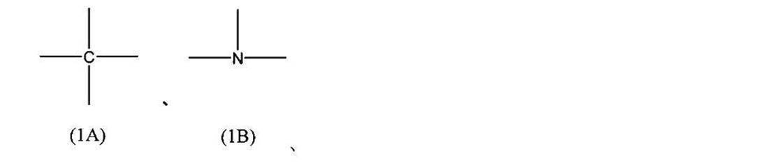
-NH-、-NR(R:アルキル基を表す)-、-O-、-S-、カルボニル基、アルキレン基、アルケニレン基、アルキニレン基、シクロアルキレン基、芳香族基、ヘテロ環基、および、これらを2種以上組み合わせた基等が挙げられる。
絶縁層前駆体層中における化合物X(または、組成物Y)の含有量は特に制限されず、絶縁層前駆体層全質量に対して、50質量%以上が好ましく、80質量%以上がより好ましい。上限としては、100質量%が挙げられる。
絶縁層前駆体層が組成物Yを含む場合、絶縁層前駆体層中における相互作用性基を有する化合物の含有量は特に制限されないが、絶縁層前駆体層全質量に対して、10~90質量%が好ましく、25~75質量%がより好ましく、35~65質量%がさらに好ましい。
なお、相互作用性基を有する化合物と重合性基を有する化合物との質量比(相互作用性基を有する化合物の質量/重合性基を有する化合物の質量)は特に制限されず、形成されるパターン状絶縁層の強度およびメッキ適性のバランスの点で、0.1~10.0が好ましく、0.5~2.0がより好ましい。
絶縁層前駆体層が組成物Yを含む場合、絶縁層前駆体層中における相互作用性基を有する化合物の含有量は特に制限されないが、絶縁層前駆体層全質量に対して、10~90質量%が好ましく、25~75質量%がより好ましく、35~65質量%がさらに好ましい。
なお、相互作用性基を有する化合物と重合性基を有する化合物との質量比(相互作用性基を有する化合物の質量/重合性基を有する化合物の質量)は特に制限されず、形成されるパターン状絶縁層の強度およびメッキ適性のバランスの点で、0.1~10.0が好ましく、0.5~2.0がより好ましい。
絶縁層前駆体層は、必要に応じて、他の成分(例えば、重合開始剤、増感剤、硬化剤、重合禁止剤、酸化防止剤、帯電防止剤、フィラー、難燃剤、滑剤、可塑剤、または、メッキ触媒若しくはその前駆体)を含んでいてもよい。
絶縁層前駆体層の形成方法は特に制限されず、例えば、化合物Xまたは組成物Yを含む組成物と基板とを接触させて、基板上に絶縁層前駆体層を形成する方法が挙げられる。
上記組成物と基板とを接触させる方法は特に制限されず、例えば、組成物を基板上に塗布する方法、または、組成物中に基板を浸漬する方法が挙げられる。
なお、必要に応じて、上記組成物と基板とを接触させた後、必要に応じて、絶縁層前駆体層から溶媒を除去するために、乾燥処理を実施してもよい。
上記組成物と基板とを接触させる方法は特に制限されず、例えば、組成物を基板上に塗布する方法、または、組成物中に基板を浸漬する方法が挙げられる。
なお、必要に応じて、上記組成物と基板とを接触させた後、必要に応じて、絶縁層前駆体層から溶媒を除去するために、乾燥処理を実施してもよい。
上記組成物は、溶媒を含んでいてもよい。溶媒の種類は特に制限されず、水および有機溶媒が挙げられる。
(工程1の手順)
工程1では、絶縁層前駆体層に露光処理および現像処理を施し、パターン状絶縁層を形成する。
露光処理においては、所望のパターン状絶縁層が得られるように、絶縁層前駆体層に対してパターン状に光照射がなされる。使用される光の種類は特に制限されず、例えば、紫外光、および、可視光が挙げられる。パターン状に光照射を行う際には、所定の形状の開口部を有するマスクを用いて光照射を行うことが好ましい。
絶縁層前駆体層の露光部においては、絶縁層前駆体層に含まれる重合性基が活性化され、化合物間の架橋が生じ、層の硬化が進行する。
露光処理の際の照射エネルギーは特に制限されないが、上述した形状の絶縁層を形成しやすい点で、300mJ/cm2以上が好ましく、400mJ/cm2以上がより好ましい。上限は特に制限されないが、2000mJ/cm2以下の場合が多い。
また、上述したポリマーZを用いて、上記照射エネルギーでの露光処理を実施すると、上述した形状の絶縁層が形成されやすい。
工程1では、絶縁層前駆体層に露光処理および現像処理を施し、パターン状絶縁層を形成する。
露光処理においては、所望のパターン状絶縁層が得られるように、絶縁層前駆体層に対してパターン状に光照射がなされる。使用される光の種類は特に制限されず、例えば、紫外光、および、可視光が挙げられる。パターン状に光照射を行う際には、所定の形状の開口部を有するマスクを用いて光照射を行うことが好ましい。
絶縁層前駆体層の露光部においては、絶縁層前駆体層に含まれる重合性基が活性化され、化合物間の架橋が生じ、層の硬化が進行する。
露光処理の際の照射エネルギーは特に制限されないが、上述した形状の絶縁層を形成しやすい点で、300mJ/cm2以上が好ましく、400mJ/cm2以上がより好ましい。上限は特に制限されないが、2000mJ/cm2以下の場合が多い。
また、上述したポリマーZを用いて、上記照射エネルギーでの露光処理を実施すると、上述した形状の絶縁層が形成されやすい。
次に、パターン状に硬化処理を施した絶縁層前駆体層に対して、現像処理を施すことにより、未露光部が除去されて、パターン状絶縁層が形成される。
現像処理の方法は特に制限されず、使用される材料の種類に応じて、最適な現像処理が実施される。現像液としては、例えば、有機溶媒、純水、および、アルカリ水溶液が挙げられる。
現像処理の方法は特に制限されず、使用される材料の種類に応じて、最適な現像処理が実施される。現像液としては、例えば、有機溶媒、純水、および、アルカリ水溶液が挙げられる。
上記手順によって形成されたパターン状絶縁層は、メッキ触媒またはその前駆体と相互作用する官能基を有する層であって、所定のパターン状に配置される層である。
パターン状絶縁層は、通常、上述した相互作用性基を有する化合物を含む。化合物としては、ポリマーが好ましい。つまり、パターン状絶縁層は、相互作用性基を有する繰り返し単位を含むポリマーを含むことが好ましい。
パターン状絶縁層は、通常、上述した相互作用性基を有する化合物を含む。化合物としては、ポリマーが好ましい。つまり、パターン状絶縁層は、相互作用性基を有する繰り返し単位を含むポリマーを含むことが好ましい。
後述する金属層は、パターン状絶縁層のパターン模様に沿って配置される。そのため、形成したい金属層の形状に合わせて、パターン状絶縁層を配置することにより、所望の形状のパターン状絶縁層が形成される。
パターン状絶縁層の厚みは特に制限されず、メッキ触媒またはその前駆体を十分に担持でき、かつ、メッキ異常を防ぐ点で、0.05μm~2.00μmが好ましく、0.10μm~1.00μmがより好ましい。
<工程2>
工程2は、絶縁層付き基板を変形させて、立体形状を有する絶縁層付き基板を得る工程である。
変形の方法は特に制限されず、公知の方法が挙げられる。変形の方法としては、例えば、真空成形、ブロー成形、フリーブロー成形、圧空成形、真空-圧空成形、および、熱プレス成形等の公知の方法が挙げられる。
工程2は、絶縁層付き基板を変形させて、立体形状を有する絶縁層付き基板を得る工程である。
変形の方法は特に制限されず、公知の方法が挙げられる。変形の方法としては、例えば、真空成形、ブロー成形、フリーブロー成形、圧空成形、真空-圧空成形、および、熱プレス成形等の公知の方法が挙げられる。
<工程3>
工程3は、立体形状を有する絶縁層付き基板のパターン状絶縁層にメッキ触媒またはその前駆体を付与する工程である。
パターン状絶縁層は上記相互作用性基を有するため、相互作用性基がその機能に応じて、付与されたメッキ触媒またはその前駆体を付着(吸着)する。
メッキ触媒またはその前駆体は、メッキ処理の触媒または電極として機能する。そのため、使用されるメッキ触媒またはその前駆体の種類は、メッキ処理の種類により適宜決定される。
工程3は、立体形状を有する絶縁層付き基板のパターン状絶縁層にメッキ触媒またはその前駆体を付与する工程である。
パターン状絶縁層は上記相互作用性基を有するため、相互作用性基がその機能に応じて、付与されたメッキ触媒またはその前駆体を付着(吸着)する。
メッキ触媒またはその前駆体は、メッキ処理の触媒または電極として機能する。そのため、使用されるメッキ触媒またはその前駆体の種類は、メッキ処理の種類により適宜決定される。
メッキ触媒またはその前駆体は、無電解メッキ触媒またはその前駆体が好ましい。
無電解メッキ触媒は、無電解メッキ時の活性核となるものであれば特に制限されず、例えば、自己触媒還元反応の触媒能を有する金属(Niよりイオン化傾向の低い無電解メッキできる金属として知られるもの)が挙げられる。具体的には、Pd、Ag、Cu、Pt、Au、および、Co等が挙げられる。
この無電解メッキ触媒としては、金属コロイドを用いてもよい。
無電解メッキ触媒前駆体は、化学反応により無電解メッキ触媒となるものであれば特に制限されず、例えば、上記無電解メッキ触媒として挙げた金属のイオンが挙げられる。
無電解メッキ触媒は、無電解メッキ時の活性核となるものであれば特に制限されず、例えば、自己触媒還元反応の触媒能を有する金属(Niよりイオン化傾向の低い無電解メッキできる金属として知られるもの)が挙げられる。具体的には、Pd、Ag、Cu、Pt、Au、および、Co等が挙げられる。
この無電解メッキ触媒としては、金属コロイドを用いてもよい。
無電解メッキ触媒前駆体は、化学反応により無電解メッキ触媒となるものであれば特に制限されず、例えば、上記無電解メッキ触媒として挙げた金属のイオンが挙げられる。
メッキ触媒またはその前駆体をパターン状絶縁層に付与する方法としては、例えば、メッキ触媒またはその前駆体を溶媒に分散または溶解させた溶液を調製し、その溶液をパターン状絶縁層上に塗布する方法、または、その溶液中に絶縁層付き基板を浸漬する方法が挙げられる。
上記溶媒としては、例えば、水または有機溶媒が挙げられる。
上記溶媒としては、例えば、水または有機溶媒が挙げられる。
<工程4>
工程4は、メッキ触媒またはその前駆体が付与されたパターン状絶縁層に対してメッキ処理を施し、金属層を形成する工程である。
メッキ処理の方法は特に制限されず、例えば、無電解メッキ処理、または、電解メッキ処理(電気メッキ処理)が挙げられる。本工程では、無電解メッキ処理を単独で実施してもよいし、無電解メッキ処理を実施した後にさらに電解メッキ処理を実施してもよい。
メッキ処理の種類は特に制限されず、例えば、銅メッキ処理、および、銀メッキ処理が挙げられる。
工程4は、メッキ触媒またはその前駆体が付与されたパターン状絶縁層に対してメッキ処理を施し、金属層を形成する工程である。
メッキ処理の方法は特に制限されず、例えば、無電解メッキ処理、または、電解メッキ処理(電気メッキ処理)が挙げられる。本工程では、無電解メッキ処理を単独で実施してもよいし、無電解メッキ処理を実施した後にさらに電解メッキ処理を実施してもよい。
メッキ処理の種類は特に制限されず、例えば、銅メッキ処理、および、銀メッキ処理が挙げられる。
以下に、実施例に基づいて本発明をさらに詳細に説明する。以下の実施例に示す材料、使用量、割合、処理内容、処理手順等は、本発明の趣旨を逸脱しない限り適宜変更することができ、本発明の範囲は、以下の実施例により限定的に解釈されるべきものではない。
<実施例1>
(基板の準備)
厚み250.00μmのポリカーボネート樹脂フィルム(帝人製パンライトPC-2151)を基板として準備した。
(基板の準備)
厚み250.00μmのポリカーボネート樹脂フィルム(帝人製パンライトPC-2151)を基板として準備した。
(プライマー層形成用組成物の調製)
以下の成分を混合し、プライマー層形成用組成物を得た。
Z913-3(アイカ工業社製) 33質量部
IPA(イソプロピルアルコール) 67質量部
以下の成分を混合し、プライマー層形成用組成物を得た。
Z913-3(アイカ工業社製) 33質量部
IPA(イソプロピルアルコール) 67質量部
(プライマー層の形成)
得られたプライマー層形成用組成物を、基板上に、平均乾燥膜厚1.00μmとなるようにバー塗布し、80℃で3分間乾燥させた。その後、形成されたプライマー層形成用組成物の層に対して、1000mJの照射量で紫外線(Ultraviolet:UV)を照射し、厚み0.80μmのプライマー層を形成した。このようにしてプライマー層が形成された基板の面を第1面とし、第1面と表裏を形成する基板の面を第2面と規定する。
得られたプライマー層形成用組成物を、基板上に、平均乾燥膜厚1.00μmとなるようにバー塗布し、80℃で3分間乾燥させた。その後、形成されたプライマー層形成用組成物の層に対して、1000mJの照射量で紫外線(Ultraviolet:UV)を照射し、厚み0.80μmのプライマー層を形成した。このようにしてプライマー層が形成された基板の面を第1面とし、第1面と表裏を形成する基板の面を第2面と規定する。
(絶縁層前駆体層形成用組成物の調製)
以下の成分を混合し、絶縁層前駆体層形成用組成物を得た。
IPA(イソプロピルアルコール) 38.00質量部
ポリブタジエンマレイン酸 4.00質量部
FAM-401(富士フイルム社製) 1.00質量部
IRGACURE OXE02(BASF社製、ClogP=6.55)
0.05質量部
以下の成分を混合し、絶縁層前駆体層形成用組成物を得た。
IPA(イソプロピルアルコール) 38.00質量部
ポリブタジエンマレイン酸 4.00質量部
FAM-401(富士フイルム社製) 1.00質量部
IRGACURE OXE02(BASF社製、ClogP=6.55)
0.05質量部
(絶縁層前駆体層付き基板の作製)
得られた絶縁層前駆体層形成用組成物をプライマー層上に膜厚0.20μmとなるようにバー塗布し、120℃の雰囲気下で1分間乾燥させた。その後、直ちに、絶縁層前駆体層形成用組成物上に厚み12.00μmのポリプロピレンフィルムを貼り合わせることにより、絶縁層前駆体層付き基板を作製した。
得られた絶縁層前駆体層形成用組成物をプライマー層上に膜厚0.20μmとなるようにバー塗布し、120℃の雰囲気下で1分間乾燥させた。その後、直ちに、絶縁層前駆体層形成用組成物上に厚み12.00μmのポリプロピレンフィルムを貼り合わせることにより、絶縁層前駆体層付き基板を作製した。
(絶縁層付き基板の作製)
絶縁層前駆体層付き基板上に、図3に示す金属メッシュMに対応する露光用パターンを有するフィルムマスクを配置し、絶縁層前駆体層付き基板に対してフィルムマスク越しに紫外線(エネルギー量500mJ/cm2、波長365μm)を照射した。次に、紫外線が照射された後の絶縁層前駆体層付き基板を純粋シャワーにより5分間現像処理し、絶縁層付き基板を作製した。
ここで、金属メッシュMに対応するフィルムマスクの露光用パターンの線幅は4.00μmとし、ピッチPは165.00μmとした。
絶縁層前駆体層付き基板上に、図3に示す金属メッシュMに対応する露光用パターンを有するフィルムマスクを配置し、絶縁層前駆体層付き基板に対してフィルムマスク越しに紫外線(エネルギー量500mJ/cm2、波長365μm)を照射した。次に、紫外線が照射された後の絶縁層前駆体層付き基板を純粋シャワーにより5分間現像処理し、絶縁層付き基板を作製した。
ここで、金属メッシュMに対応するフィルムマスクの露光用パターンの線幅は4.00μmとし、ピッチPは165.00μmとした。
(立体成形)
真空引きのための複数の貫通孔を有する型治具に絶縁層付き基板を配置して、絶縁層付き基板の温度が約160℃となるまで絶縁層付き基板を加熱した。さらに、絶縁層付き基板の温度が約160℃となったところで型治具の真空引きを実施することにより、絶縁層付き基板を型治具に密着させて、絶縁層付き基板を図1に示すような半球の曲面に沿った形状に立体成形した。
真空引きのための複数の貫通孔を有する型治具に絶縁層付き基板を配置して、絶縁層付き基板の温度が約160℃となるまで絶縁層付き基板を加熱した。さらに、絶縁層付き基板の温度が約160℃となったところで型治具の真空引きを実施することにより、絶縁層付き基板を型治具に密着させて、絶縁層付き基板を図1に示すような半球の曲面に沿った形状に立体成形した。
(金属層の形成)
立体成形された絶縁層付き基板を、35℃の1質量%の炭酸水素ナトリウム水溶液に5分間浸漬させた。次に、絶縁層付き基板を、55℃のパラジウム触媒付与液RONAMERSE SMT(ロームアンドハース電子材料株式会社製)に5分間浸漬させた。絶縁層付き基板を水洗した後、続けて35℃のCIRCUPOSIT6540(ロームアンドハース電子材料株式会社製)に5分間浸漬させ、その後、再び水洗した。さらに、絶縁層付き基板を、45℃のCIRCUPOSIT4500(ロームアンドハース電子材料株式会社製)に20分間浸漬させた後、水洗して、絶縁層上に金属層を形成した。これにより、基板上に、図4に示す断面形状を有する銅製の複数の金属細線からなる導電膜を有する導電膜付き基板を得た。
立体成形された絶縁層付き基板を、35℃の1質量%の炭酸水素ナトリウム水溶液に5分間浸漬させた。次に、絶縁層付き基板を、55℃のパラジウム触媒付与液RONAMERSE SMT(ロームアンドハース電子材料株式会社製)に5分間浸漬させた。絶縁層付き基板を水洗した後、続けて35℃のCIRCUPOSIT6540(ロームアンドハース電子材料株式会社製)に5分間浸漬させ、その後、再び水洗した。さらに、絶縁層付き基板を、45℃のCIRCUPOSIT4500(ロームアンドハース電子材料株式会社製)に20分間浸漬させた後、水洗して、絶縁層上に金属層を形成した。これにより、基板上に、図4に示す断面形状を有する銅製の複数の金属細線からなる導電膜を有する導電膜付き基板を得た。
(黒化処理)
得られた導電膜付き基板を、30℃のOPCブラックカッパー(奥野製薬工業株式会社製)に3分間浸漬させ、水洗し、金属層上に黒化層を形成した。これにより、実施例1の透明導電膜基材を得た。この透明導電膜基材のシート抵抗を測定したところ、0.50Ω/□であった。
得られた導電膜付き基板を、30℃のOPCブラックカッパー(奥野製薬工業株式会社製)に3分間浸漬させ、水洗し、金属層上に黒化層を形成した。これにより、実施例1の透明導電膜基材を得た。この透明導電膜基材のシート抵抗を測定したところ、0.50Ω/□であった。
(可視光透過率の測定)
日本電色工業社製分光ヘーズメーターSH7000を用い、可視光の測定範囲を380nm~780nmとして、実施例1の透明導電膜基材の可視光透過率を測定した。実施例1の透明導電膜基材の可視光透過率は、76.0%であった。
日本電色工業社製分光ヘーズメーターSH7000を用い、可視光の測定範囲を380nm~780nmとして、実施例1の透明導電膜基材の可視光透過率を測定した。実施例1の透明導電膜基材の可視光透過率は、76.0%であった。
(金属細線の断面形状の計測)
実施例1の透明導電膜基材における金属細線を線幅方向に切断し、その断面を日立ハイテクノロジーズ社製SEM(Scanning Electron Microscope:走査型電子顕微鏡)S-3000Nにより撮像し、得られた電子顕微鏡画像を観察したところ、金属細線は、図4に示すような台形の断面形状を有していた。そこで、電子顕微鏡画像を用いて、絶縁層の上底部の線幅、下底部の線幅W2、金属細線の線幅W1すなわち金属層の線幅W1および導電膜の厚みを計測した。特に、導電膜の厚みは、線幅方向における下底部の両端部のそれぞれから黒化層の表面までの長さと、下底部の中央から黒化層の表面までの長さをそれぞれ計測し、それらの平均値を算出することにより計測した。
実施例1の透明導電膜基材における金属細線を線幅方向に切断し、その断面を日立ハイテクノロジーズ社製SEM(Scanning Electron Microscope:走査型電子顕微鏡)S-3000Nにより撮像し、得られた電子顕微鏡画像を観察したところ、金属細線は、図4に示すような台形の断面形状を有していた。そこで、電子顕微鏡画像を用いて、絶縁層の上底部の線幅、下底部の線幅W2、金属細線の線幅W1すなわち金属層の線幅W1および導電膜の厚みを計測した。特に、導電膜の厚みは、線幅方向における下底部の両端部のそれぞれから黒化層の表面までの長さと、下底部の中央から黒化層の表面までの長さをそれぞれ計測し、それらの平均値を算出することにより計測した。
実施例1の透明導電膜基材における絶縁層の下底部の線幅W2は8.00μm、上底部の線幅は4.00μmであり、下底部の線幅W2に対する上底部の線幅の比率は、4.00/8.00=0.50であった。また、金属層の線幅W1は、12.50μmであった。そのため、金属細線の線幅方向において、絶縁層の片側の端部よりも外側に存在する金属層の部分の幅(W1-W2)/2は、(12.50μm-8.00μm)/2=2.25μmであった。また、金属層の線幅W1を4で除した値は、3.13μmであった。また、導電膜の厚みは2.20μmであった。
(散乱反射率の測定)
積分球付属装置付きの分光光度計V-670(日本分光株式会社製)を用いて、基板の第1面側から入射する380nm~800nmの波長範囲の電磁波(可視光)に対する、実施例1の透明導電膜基材の散乱反射率を計測した。また、分光光度計V-670を用いて、基板の第1面側から入射する1050nm~1070nmの波長範囲の電磁波に対する、実施例1の透明導電膜基材の散乱反射率Aと、基板の第2面側から入射する1050nm~1070nmの波長範囲の電磁波に対する実施例1の透明導電膜基材の散乱反射率Bを計測し、比率A/Bを算出した。
積分球付属装置付きの分光光度計V-670(日本分光株式会社製)を用いて、基板の第1面側から入射する380nm~800nmの波長範囲の電磁波(可視光)に対する、実施例1の透明導電膜基材の散乱反射率を計測した。また、分光光度計V-670を用いて、基板の第1面側から入射する1050nm~1070nmの波長範囲の電磁波に対する、実施例1の透明導電膜基材の散乱反射率Aと、基板の第2面側から入射する1050nm~1070nmの波長範囲の電磁波に対する実施例1の透明導電膜基材の散乱反射率Bを計測し、比率A/Bを算出した。
この際に、分光光度計V-670に積分球ユニットISN723型を組み合わせて全角度測定値を計測し、分光光度計V-670に絶対反射率測定ユニットARV4745型を組み合わせて正反射率を計測し、全角度測定値から正反射率を差し引くことにより、散乱反射率を算出した。さらに、同様の測定を実施例1の透明導電膜基材における複数個所で実施し、得られた散乱反射率を平均したものを、最終的な散乱反射率とした。
基板の第1面側から入射する380nm~800nmの波長範囲の電磁波に対する、実施例1の透明導電膜基材の散乱反射率は、2.5%であった。また、基板の第1面側から入射する1050nm~1070nmの波長範囲の電磁波に対する散乱反射率Aは4.0%、散乱反射率Bは0.7%であり、比率A/Bは、5.7であった。
<実施例2>
絶縁層付き基板の作製工程において、絶縁層前駆体に照射したUV光の照射エネルギーを350mJ/cm2とした以外は、実施例1と同様にして、透明導電膜基材を作製した。この透明導電膜基材のシート抵抗は0.60Ω/□であり、可視光透過率は、78.0%であった。
絶縁層付き基板の作製工程において、絶縁層前駆体に照射したUV光の照射エネルギーを350mJ/cm2とした以外は、実施例1と同様にして、透明導電膜基材を作製した。この透明導電膜基材のシート抵抗は0.60Ω/□であり、可視光透過率は、78.0%であった。
また、実施例2の透明導電膜基材において、絶縁層の下底部の線幅W2は7.00μmであり、上底部の線幅は4.00μmであった。そのため、下底部の線幅W2に対する上底部の線幅の比率は、4.00/7.00≒0.57であった。
また、金属層の線幅W1は、12.00μmであった。そのため、金属細線の線幅方向において、絶縁層の片側の端部よりも外側に存在する金属層の部分の幅(W1-W2)/2は、(12.00μm-7.00μm)/2=2.50μmであった。また、金属層の線幅W1を4で除した値は、3.00μmであった。
また、導電膜の厚みは、2.30μmであった。また、基板の第1面側から入射する380nm~800nmの波長範囲の電磁波に対する、実施例2の透明導電膜基材の散乱反射率は、2.0%であった。また、散乱反射率Aは3.6%、散乱反射率Bは0.7%であり、比率A/Bは、5.1であった。
また、導電膜の厚みは、2.30μmであった。また、基板の第1面側から入射する380nm~800nmの波長範囲の電磁波に対する、実施例2の透明導電膜基材の散乱反射率は、2.0%であった。また、散乱反射率Aは3.6%、散乱反射率Bは0.7%であり、比率A/Bは、5.1であった。
<実施例3>
絶縁層付き基板の作製工程において、絶縁層前駆体に照射したUV光の照射エネルギーを270mJ/cm2とした以外は、実施例1と同様にして、透明導電膜基材を作製した。この透明導電膜基材のシート抵抗は0.65Ω/□であり、可視光透過率は78.5%であった。
絶縁層付き基板の作製工程において、絶縁層前駆体に照射したUV光の照射エネルギーを270mJ/cm2とした以外は、実施例1と同様にして、透明導電膜基材を作製した。この透明導電膜基材のシート抵抗は0.65Ω/□であり、可視光透過率は78.5%であった。
また、実施例3の透明導電膜基材において、絶縁層の下底部の線幅W2は5.50μmであり、上底部の線幅は4.00μmであった。そのため、下底部の線幅W2に対する上底部の線幅の比率は、4.00/5.50≒0.73であった。
また、金属層の線幅W1は、11.50μmであった。そのため、金属細線の線幅方向において、絶縁層の片側の端部よりも外側に存在する金属層の部分の幅(W1-W2)/2は、(11.50μm-5.50μm)/2=3.00μmであった。また、金属層の線幅W1を4で除した値は、2.93μmであった。
また、導電層の厚みは、2.30μmであった。また、基板の第1面側から入射する380nm~800nmの波長範囲の電磁波に対する、実施例3の透明導電膜基材の散乱反射率は、2.0%であった。また、散乱反射率Aは3.4%、散乱反射率Bは0.8%であり、比率A/Bは、4.3であった。
また、導電層の厚みは、2.30μmであった。また、基板の第1面側から入射する380nm~800nmの波長範囲の電磁波に対する、実施例3の透明導電膜基材の散乱反射率は、2.0%であった。また、散乱反射率Aは3.4%、散乱反射率Bは0.8%であり、比率A/Bは、4.3であった。
<比較例1>
絶縁層付き基板の作製工程において、絶縁層前駆体に照射したUV光の照射エネルギーを200mJ/cm2とした以外は、実施例1と同様にして、透明導電膜基材を作製した。この透明導電膜基材のシート抵抗は0.70Ω/□であり、可視光透過率は80.0%であった。
絶縁層付き基板の作製工程において、絶縁層前駆体に照射したUV光の照射エネルギーを200mJ/cm2とした以外は、実施例1と同様にして、透明導電膜基材を作製した。この透明導電膜基材のシート抵抗は0.70Ω/□であり、可視光透過率は80.0%であった。
比較例1の透明導電膜基材において、絶縁層は、図5に示すような概ね長方形の断面形状を有していた。絶縁層の下底部の線幅W2と上底部の線幅は、いずれも4.00μmであり、下底部の線幅W2に対する上底部の線幅の比率は、4.00/4.00=1.00であった。
また、金属層の線幅W1は、10.50μmであった。そのため、金属細線の線幅方向において、絶縁層の片側の端部よりも外側に存在する金属層の部分の幅(W1-W2)/2は、(12.00μm-4.00μm)/2=4.00μmであった。また、金属層の線幅W1を4で除した値は、2.63μmであった。
また、導電膜の厚みは、2.40μmであった。また、基板の第1面側から入射する380nm~800nmの波長範囲の電磁波に対する、実施例2の透明導電膜基材の散乱反射率は、2.0%であった。また、散乱反射率Aは2.9%、散乱反射率Bは1.5%であり、比率A/Bは、1.9であった。
また、導電膜の厚みは、2.40μmであった。また、基板の第1面側から入射する380nm~800nmの波長範囲の電磁波に対する、実施例2の透明導電膜基材の散乱反射率は、2.0%であった。また、散乱反射率Aは2.9%、散乱反射率Bは1.5%であり、比率A/Bは、1.9であった。
<比較例2>
黒化処理を実施しない以外は、実施例1と同様にして、透明導電膜基材を作製した。この透明導電膜基材のシート抵抗は0.50Ω/□であり、可視光透過率は76.0%であった。
黒化処理を実施しない以外は、実施例1と同様にして、透明導電膜基材を作製した。この透明導電膜基材のシート抵抗は0.50Ω/□であり、可視光透過率は76.0%であった。
また、比較例2の透明導電膜基材において、絶縁層の下底部の線幅W2は8.00μmであり、上底部の線幅は4.00μmであった。そのため、下底部の線幅W2に対する上底部の線幅の比率は、4.00/8.00=0.50であった。
また、金属層の線幅W1は、12.50μmであった。そのため、金属細線の線幅方向において、絶縁層の片側の端部よりも外側に存在する金属層の部分の幅(W1-W2)/2は、(12.50μm-8.00μm)/2=2.25μmであった。また、金属層の線幅W1を4で除した値は、3.13μmであった。
また、導電膜の厚みは、2.20μmであった。また、基板の第1面側から入射する380nm~800nmの波長範囲の電磁波に対する、実施例2の透明導電膜基材の散乱反射率は、8.0%であった。また、散乱反射率Aは13.0%、散乱反射率Bは1.6%であり、比率A/Bは、8.1であった。
また、導電膜の厚みは、2.20μmであった。また、基板の第1面側から入射する380nm~800nmの波長範囲の電磁波に対する、実施例2の透明導電膜基材の散乱反射率は、8.0%であった。また、散乱反射率Aは13.0%、散乱反射率Bは1.6%であり、比率A/Bは、8.1であった。
(第1面側の視認性評価)
実施例1~3、比較例1および2の透明導電膜基材を、それぞれ、基板の第1面側から観察することにより、それぞれの透明導電膜基材の第1面側の視認性を評価した。具体的には、3人の観察者が実施例1~3、比較例1および2の透明導電膜基材を観察し、導電膜における複数の金属細線が目立って視認されない場合に視認性が良好である(○)という評価を下し、導電膜における複数の金属細線が目立って視認される場合に視認性が悪い(×)であるという評価を下した。3人の観察者の下した評価のうち、最も多い評価結果を最終的な評価結果とした。
実施例1~3、比較例1および2の透明導電膜基材を、それぞれ、基板の第1面側から観察することにより、それぞれの透明導電膜基材の第1面側の視認性を評価した。具体的には、3人の観察者が実施例1~3、比較例1および2の透明導電膜基材を観察し、導電膜における複数の金属細線が目立って視認されない場合に視認性が良好である(○)という評価を下し、導電膜における複数の金属細線が目立って視認される場合に視認性が悪い(×)であるという評価を下した。3人の観察者の下した評価のうち、最も多い評価結果を最終的な評価結果とした。
(S/N比の評価)
実施例1~3、比較例1および2の透明導電膜基材に対して、それぞれ、基板の第2面側にLider(Light detection and ranging:光検出および測距)センサを設置し、Liderセンサを用いて、このLiderセンサから5m離れた対象物の距離を測定した。また、実施例1~3、比較例1および2の透明導電膜基材の代わりに、厚み250.00μmのポリカーボネート樹脂フィルム(帝人製パンライトPC-2151)を配置した状態で、Liderセンサにより、Liderセンサから5m離れた対象物の距離を測定した。
実施例1~3、比較例1および2の透明導電膜基材に対して、それぞれ、基板の第2面側にLider(Light detection and ranging:光検出および測距)センサを設置し、Liderセンサを用いて、このLiderセンサから5m離れた対象物の距離を測定した。また、実施例1~3、比較例1および2の透明導電膜基材の代わりに、厚み250.00μmのポリカーボネート樹脂フィルム(帝人製パンライトPC-2151)を配置した状態で、Liderセンサにより、Liderセンサから5m離れた対象物の距離を測定した。
このようにして計測された、実施例1~3、比較例1および2の透明導電膜基材の代わりにポリカーボネート樹脂フィルムを配置した場合の距離の測定値に対する、実施例1~3、比較例1および2の透明導電膜基材を配置した場合の距離の測定値の比率が、+200%未満の場合を「◎」、+200%以上+500%未満の場合を「○」、+500%以上+1000%未満の場合を「△」、+1000%以上の場合を「×」とした。なお、◎が最もS/N比が小さく、「◎」、「〇」、「△」、「×」の順にS/N比が大きいことを表している。また、「◎」は優れたレベル、「〇」は良好なレベル、「△」は実用上問題がないレベル、「×」は実用上問題があるレベルである。
以下の表1に、実施例1~3、比較例1および2の評価結果を示す。
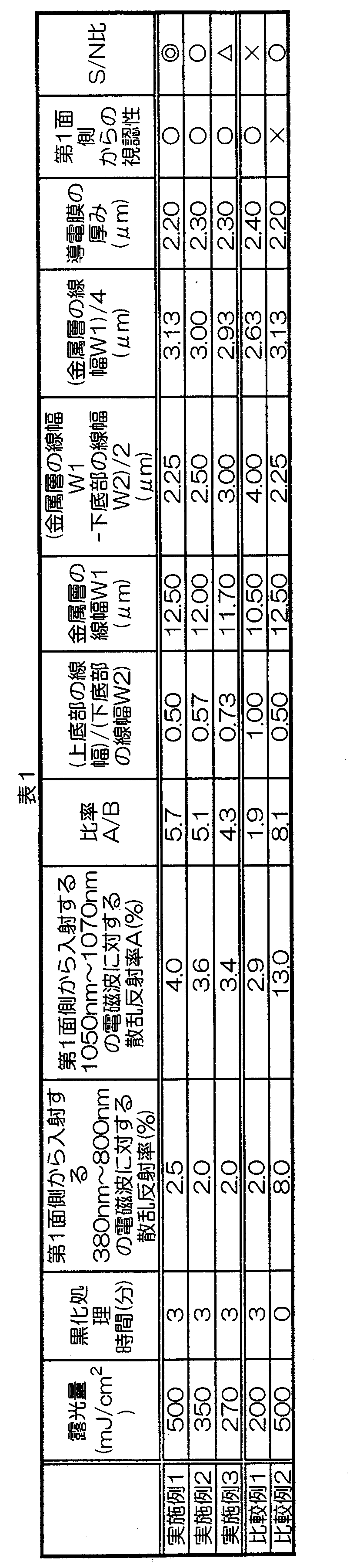
表1に示すように、実施例1~実施例3の透明導電膜基材は、第1面側からの視認性評価がいずれも「○」であり、S/N比の評価については、実施例1の透明導電膜基材は「◎」、実施例2の透明導電膜基材は「○」、実施例3の透明導電膜基材は「△」であった。
実施例1~実施例3では、基板の第1面側から入射する380nm~800nmの波長範囲の電磁波に対する散乱反射率がいずれも5%未満であり、比率A/Bがいずれも4.0より大きい。
また、実施例1では、(金属層の線幅W1-下底部の線幅W2)/2が2.25μmであり、3.00μm未満で且つ金属層の線幅W1の1/4である3.13μm未満である。また、実施例2では、(金属層の線幅W1-下底部の線幅W2)/2が2.50μmであり、金属層の線幅W1の1/4である3.00μm未満である。
また、実施例3では、(金属層の線幅W1-下底部の線幅W2)/2が3.00μmであり、金属層の線幅W1の1/4である2.93よりも大きい。
また、実施例3では、(金属層の線幅W1-下底部の線幅W2)/2が3.00μmであり、金属層の線幅W1の1/4である2.93よりも大きい。
このように、実施例1~実施例3の透明導電膜基材では、黒化層が形成されることにより、第1面側からの可視光の散乱反射が抑制されるため、優れた視認性が得られたと考えられる。また、金属細線の線幅方向において金属層が絶縁層からはみ出すことが抑制されるため、基板の第1面側において優れた視認性を有していながらも、基板の第2面側に配置されたセンサが検出する信号においてノイズが含まれにくいことがわかる。
また、S/N比の評価結果が特に優れている実施例1および実施例2の透明導電膜基材は、(W1-W2)/2<3.00μm、且つ、(W1-W2)/2<(W1)/4の関係を満たしていることが分かる。そのため、ノイズを抑制するためには、特に、(W1-W2)/2<3.00μm、且つ、(W1-W2)/2<(W1)/4の関係を満たすことが好ましい。
これに対して、比較例1の透明導電膜基材は、基板の第1面側からの視認性評価は「○」であったが、S/N比の評価は「×」であった。比較例1では、線幅方向において絶縁層の片側からの金属層が4.00μmはみ出しており、このはみ出し部分により、基板の第2面側から入射する電磁波が散乱反射しやすくなっているからであると考えられる。
また、線幅方向において絶縁層の片側からの金属層が4.00μmはみ出しているのは、絶縁層が概ね長方形の断面形状を有しており、線幅方向における絶縁層の両端部の壁面上での金属の析出量が多いためであると考えられる。
さらに、絶縁層が概ね長方形の断面形状を有しているのは、絶縁層付き基板の作製工程において絶縁層前駆体に照射したUV光の照射エネルギーが200mJ/cm2と低いため、UV光が照射された際にフィルムマスクの露光用パターンの端部で発生する回折光の強度が弱く、絶縁層前駆体層の硬化に回折光がほとんど寄与しなかったからであると考えられる。
また、比較例2の透明導電膜基材は、S/N比の評価が「○」であるが、第1面側からの視認性評価が「×」であった。これは、金属層上に黒化層が形成されていないために、基板の第1面側から入射する380nm~800nmの波長範囲の電磁波に対する散乱反射率が8%となり、金属層の表面で可視光が反射して、金属細線が目立って視認されたからであると考えられる。
本発明は、基本的に以上のように構成されるものである。以上において、本発明の透明導電膜基材について詳細に説明したが、本発明は、上述の実施態様に限定されず、本発明の主旨を逸脱しない範囲において、種々の改良または変更をしてもよいのはもちろんである。
11 透明導電膜基材、12,22 基板、12A,22A 第1面、12B,22B 第2面、13 導電膜、14,24 金属細線、15 開口部、16,26 絶縁層、16A 下底部、16B 上底部、17,27 金属層、18,28 黒化層、19 センサ装置、A1 センサ、CL 中心線、M 金属メッシュ、P ピッチ、W,W1~W5 線幅。
Claims (18)
- 表裏を形成する第1面と第2面を有する基板と、
前記基板の少なくとも前記第1面上に形成された導電膜を有し、
前記第1面側から入射する380nm~800nmの波長範囲の電磁波に対して5%未満の散乱反射率を有し、
前記第1面側から入射する1050nm~1070nmの波長範囲の電磁波に対して5%未満の散乱反射率Aを有し、
前記散乱反射率Aと、前記第2面側から入射する1050nm~1070nmの波長範囲の電磁波に対する散乱反射率Bとは、A/B>4.0の関係を満たし、
前記導電膜は、2.00μm以上の膜厚を有する
透明導電膜基材。 - 前記基板の前記第1面上および前記第2面上に、前記導電膜が形成される請求項1に記載の透明導電膜基材。
- 前記導電膜は、0.1Ω/□以上10.0Ω/□以下のシート抵抗を有する請求項1または2に記載の透明導電膜基材。
- 立体形状を有する請求項1~3のいずれか一項に記載の透明導電膜基材。
- 前記導電膜は、複数の金属細線により形成されるメッシュ形状を有する請求項1~4のいずれか一項に記載の透明導電膜基材。
- 前記金属細線は、20.00μm以下の線幅を有する請求項5に記載の透明導電膜基材。
- 前記金属細線は、前記基板上に形成された絶縁層と、前記絶縁層を覆うように前記絶縁層上に形成された金属層を含む請求項5または6に記載の透明導電膜基材。
- 前記金属細線における前記金属層の線幅をW1、前記金属細線における前記絶縁層の線幅をW2として、前記金属細線の線幅方向において、前記絶縁層の端部よりも外側に存在する前記金属層の部分の幅(W1-W2)/2は、(W1-W2)/2<3.00μm、且つ、(W1-W2)/2<(W1)/4を満たす請求項7に記載の透明導電膜基材。
- 前記絶縁層は、前記基板に接する下底部と、前記下底部の線幅よりも狭い線幅を有し且つ前記絶縁層の線幅方向における中央部に位置する上底部を有し、前記線幅方向における両端部の厚みが前記上底部と前記下底部との間の厚みよりも薄い請求項7または8に記載の透明導電膜基材。
- 前記絶縁層は、前記線幅方向において、前記上底部の両端部から前記下底部の両端部にかけて徐々に厚みが減少する形状を有する請求項9に記載の透明導電膜基材。
- 前記絶縁層は、樹脂を主成分とする請求項7~10のいずれか一項に記載の透明導電膜基材。
- 前記絶縁層は、メッキ触媒と相互作用する相互作用性基を有するポリマーを含む請求項11に記載の透明導電膜基材。
- 前記相互作用性基を有する前記ポリマーは、前記絶縁層において3次元網目構造を有する請求項12に記載の透明導電膜基材。
- 前記金属層は、銅、銀およびアルミニウムのいずれかを主成分として含む請求項7~13のいずれか一項に記載の透明導電膜基材。
- 前記基板は、ポリカーボネート樹脂、ポリメタクリル酸メチル樹脂、アクリロニトリルブタジエンスチレン樹脂およびポリエチレンテレフタラート樹脂のいずれかを主成分として含む請求項1~14のいずれか一項に記載の透明導電膜基材。
- 可視光透過率が75%以上である請求項1~15のいずれか一項に記載の透明導電膜基材。
- 請求項1~16のいずれか一項に記載の透明導電膜基材と、
電磁波を照射するセンサと
を備え、
前記透明導電膜基材は、前記センサに対して、前記センサにより照射される電磁波の照射方向に配置されるセンサ装置。 - 前記透明導電膜基材は、前記第2面が前記センサに対向するように配置される請求項17に記載のセンサ装置。
Priority Applications (1)
| Application Number | Priority Date | Filing Date | Title |
|---|---|---|---|
| JP2022551920A JP7500747B2 (ja) | 2020-09-25 | 2021-09-15 | 透明導電膜基材およびセンサ装置 |
Applications Claiming Priority (2)
| Application Number | Priority Date | Filing Date | Title |
|---|---|---|---|
| JP2020-160802 | 2020-09-25 | ||
| JP2020160802 | 2020-09-25 |
Publications (1)
| Publication Number | Publication Date |
|---|---|
| WO2022065161A1 true WO2022065161A1 (ja) | 2022-03-31 |
Family
ID=80846471
Family Applications (1)
| Application Number | Title | Priority Date | Filing Date |
|---|---|---|---|
| PCT/JP2021/033954 Ceased WO2022065161A1 (ja) | 2020-09-25 | 2021-09-15 | 透明導電膜基材およびセンサ装置 |
Country Status (2)
| Country | Link |
|---|---|
| JP (1) | JP7500747B2 (ja) |
| WO (1) | WO2022065161A1 (ja) |
Cited By (1)
| Publication number | Priority date | Publication date | Assignee | Title |
|---|---|---|---|---|
| WO2026005144A1 (ko) * | 2024-06-25 | 2026-01-02 | 주식회사 케이앤에스아이앤씨 | 고내수압을 갖는 잠수함용 위성안테나 레이돔 |
Citations (3)
| Publication number | Priority date | Publication date | Assignee | Title |
|---|---|---|---|---|
| JP2006339526A (ja) * | 2005-06-03 | 2006-12-14 | Fujifilm Holdings Corp | 透光性電磁波シールド膜の製造方法および透光性電磁波シールド膜 |
| JP2015005495A (ja) * | 2013-05-24 | 2015-01-08 | 富士フイルム株式会社 | 透明導電膜、透明導電膜の製造方法、タッチパネル及び表示装置 |
| JP2020005057A (ja) * | 2018-06-26 | 2020-01-09 | Nissha株式会社 | 電磁波透過性カバー及びその製造方法 |
-
2021
- 2021-09-15 JP JP2022551920A patent/JP7500747B2/ja active Active
- 2021-09-15 WO PCT/JP2021/033954 patent/WO2022065161A1/ja not_active Ceased
Patent Citations (3)
| Publication number | Priority date | Publication date | Assignee | Title |
|---|---|---|---|---|
| JP2006339526A (ja) * | 2005-06-03 | 2006-12-14 | Fujifilm Holdings Corp | 透光性電磁波シールド膜の製造方法および透光性電磁波シールド膜 |
| JP2015005495A (ja) * | 2013-05-24 | 2015-01-08 | 富士フイルム株式会社 | 透明導電膜、透明導電膜の製造方法、タッチパネル及び表示装置 |
| JP2020005057A (ja) * | 2018-06-26 | 2020-01-09 | Nissha株式会社 | 電磁波透過性カバー及びその製造方法 |
Cited By (1)
| Publication number | Priority date | Publication date | Assignee | Title |
|---|---|---|---|---|
| WO2026005144A1 (ko) * | 2024-06-25 | 2026-01-02 | 주식회사 케이앤에스아이앤씨 | 고내수압을 갖는 잠수함용 위성안테나 레이돔 |
Also Published As
| Publication number | Publication date |
|---|---|
| JP7500747B2 (ja) | 2024-06-17 |
| JPWO2022065161A1 (ja) | 2022-03-31 |
Similar Documents
| Publication | Publication Date | Title |
|---|---|---|
| JP6340378B2 (ja) | 導電性積層体の製造方法、導電性積層体、タッチセンサー | |
| CN106662939B (zh) | 触控面板用导电性层积体、触控面板、透明导电性层积体 | |
| KR102035404B1 (ko) | 피도금층 형성용 조성물, 피도금층 전구체층 부착 필름, 패턴 형상 피도금층 부착 필름, 도전성 필름, 터치 패널 | |
| TW201734740A (zh) | 導電性積層體的製造方法以及帶被鍍覆層前驅體層的立體結構物、帶圖案狀被鍍覆層的立體結構物、導電性積層體、觸控感測器、發熱構件及立體結構物 | |
| JPWO2015190484A6 (ja) | タッチパネル用導電性積層体、タッチパネル、透明導電性積層体 | |
| JPWO2018168243A1 (ja) | 導電性積層体の製造方法、導電性積層体、及び、タッチセンサ | |
| JP7402908B2 (ja) | 導電性部材、タッチパネルセンサー、タッチパネル、成形体の製造方法 | |
| WO2022065161A1 (ja) | 透明導電膜基材およびセンサ装置 | |
| TWI804580B (zh) | 前驅物薄膜、附被鍍層基板、導電性薄膜、觸控面板感測器、觸控面板、導電性薄膜的製造方法及被鍍層形成用組成物 | |
| WO2020196010A1 (ja) | 導電性基板の製造方法 | |
| JP6923749B2 (ja) | 導電性フィルム、タッチパネルセンサー、タッチパネル | |
| WO2016158419A1 (ja) | タッチパネルセンサー用導電性フィルムの製造方法、タッチパネルセンサー用導電性フィルム、および、タッチパネル | |
| JP2023031084A (ja) | 透明発熱体 | |
| JP2023034580A (ja) | 透明発熱体、車載ヘッドランプカバーおよびセンサーカバー | |
| CN113631369B (zh) | 层叠体、附被镀覆层基板的制造方法、导电性薄膜的制造方法 | |
| US20250013335A1 (en) | Touch sensor and touch panel | |
| US20240321482A1 (en) | Conductive film | |
| WO2023048204A1 (ja) | 積層体の製造方法、積層体 | |
| JP2023066192A (ja) | 積層体、導電性基板の製造方法 | |
| JP2020050835A (ja) | 被めっき層形成用組成物、被めっき層前駆体層付き基板、被めっき層付き基板、導電性フィルム、タッチパネルセンサー、タッチパネル |
Legal Events
| Date | Code | Title | Description |
|---|---|---|---|
| 121 | Ep: the epo has been informed by wipo that ep was designated in this application |
Ref document number: 21872291 Country of ref document: EP Kind code of ref document: A1 |
|
| ENP | Entry into the national phase |
Ref document number: 2022551920 Country of ref document: JP Kind code of ref document: A |
|
| NENP | Non-entry into the national phase |
Ref country code: DE |
|
| 122 | Ep: pct application non-entry in european phase |
Ref document number: 21872291 Country of ref document: EP Kind code of ref document: A1 |