WO2022059445A1 - アンテナ装置 - Google Patents
アンテナ装置 Download PDFInfo
- Publication number
- WO2022059445A1 WO2022059445A1 PCT/JP2021/031213 JP2021031213W WO2022059445A1 WO 2022059445 A1 WO2022059445 A1 WO 2022059445A1 JP 2021031213 W JP2021031213 W JP 2021031213W WO 2022059445 A1 WO2022059445 A1 WO 2022059445A1
- Authority
- WO
- WIPO (PCT)
- Prior art keywords
- ground plane
- radiating element
- edge
- antenna device
- stub
- Prior art date
- Legal status (The legal status is an assumption and is not a legal conclusion. Google has not performed a legal analysis and makes no representation as to the accuracy of the status listed.)
- Ceased
Links
Images






Classifications
-
- H—ELECTRICITY
- H01—ELECTRIC ELEMENTS
- H01Q—ANTENNAS, i.e. RADIO AERIALS
- H01Q9/00—Electrically-short antennas having dimensions not more than twice the operating wavelength and consisting of conductive active radiating elements
- H01Q9/04—Resonant antennas
- H01Q9/0407—Substantially flat resonant element parallel to ground plane, e.g. patch antenna
- H01Q9/0414—Substantially flat resonant element parallel to ground plane, e.g. patch antenna in a stacked or folded configuration
-
- H—ELECTRICITY
- H01—ELECTRIC ELEMENTS
- H01Q—ANTENNAS, i.e. RADIO AERIALS
- H01Q9/00—Electrically-short antennas having dimensions not more than twice the operating wavelength and consisting of conductive active radiating elements
- H01Q9/04—Resonant antennas
- H01Q9/0407—Substantially flat resonant element parallel to ground plane, e.g. patch antenna
- H01Q9/0421—Substantially flat resonant element parallel to ground plane, e.g. patch antenna with a shorting wall or a shorting pin at one end of the element
-
- H—ELECTRICITY
- H01—ELECTRIC ELEMENTS
- H01Q—ANTENNAS, i.e. RADIO AERIALS
- H01Q1/00—Details of, or arrangements associated with, antennas
- H01Q1/52—Means for reducing coupling between antennas; Means for reducing coupling between an antenna and another structure
- H01Q1/521—Means for reducing coupling between antennas; Means for reducing coupling between an antenna and another structure reducing the coupling between adjacent antennas
- H01Q1/523—Means for reducing coupling between antennas; Means for reducing coupling between an antenna and another structure reducing the coupling between adjacent antennas between antennas of an array
-
- H—ELECTRICITY
- H01—ELECTRIC ELEMENTS
- H01Q—ANTENNAS, i.e. RADIO AERIALS
- H01Q19/00—Combinations of primary active antenna elements and units with secondary devices, e.g. with quasi-optical devices, for giving the antenna a desired directional characteristic
- H01Q19/005—Patch antenna using one or more coplanar parasitic elements
-
- H—ELECTRICITY
- H01—ELECTRIC ELEMENTS
- H01Q—ANTENNAS, i.e. RADIO AERIALS
- H01Q21/00—Antenna arrays or systems
- H01Q21/06—Arrays of individually energised antenna units similarly polarised and spaced apart
- H01Q21/08—Arrays of individually energised antenna units similarly polarised and spaced apart the units being spaced along or adjacent to a rectilinear path
-
- H—ELECTRICITY
- H01—ELECTRIC ELEMENTS
- H01Q—ANTENNAS, i.e. RADIO AERIALS
- H01Q5/00—Arrangements for simultaneous operation of antennas on two or more different wavebands, e.g. dual-band or multi-band arrangements
- H01Q5/30—Arrangements for providing operation on different wavebands
- H01Q5/307—Individual or coupled radiating elements, each element being fed in an unspecified way
- H01Q5/314—Individual or coupled radiating elements, each element being fed in an unspecified way using frequency dependent circuits or components, e.g. trap circuits or capacitors
- H01Q5/335—Individual or coupled radiating elements, each element being fed in an unspecified way using frequency dependent circuits or components, e.g. trap circuits or capacitors at the feed, e.g. for impedance matching
-
- H—ELECTRICITY
- H01—ELECTRIC ELEMENTS
- H01Q—ANTENNAS, i.e. RADIO AERIALS
- H01Q9/00—Electrically-short antennas having dimensions not more than twice the operating wavelength and consisting of conductive active radiating elements
- H01Q9/04—Resonant antennas
- H01Q9/16—Resonant antennas with feed intermediate between the extremities of the antenna, e.g. centre-fed dipole
- H01Q9/28—Conical, cylindrical, cage, strip, gauze, or like elements having an extended radiating surface; Elements comprising two conical surfaces having collinear axes and adjacent apices and fed by two-conductor transmission lines
- H01Q9/285—Planar dipole
Definitions
- the present invention relates to an antenna device.
- Patent Document 1 discloses a patch antenna (referred to as a half patch antenna in the present specification) in which one side (rear edge) of the radiating element is short-circuited and the area of the radiating element is reduced to about 1/2.
- desired radiation characteristics are obtained by shortening the lateral distance between the front edge opposite to the rear edge of the radiation element and the corresponding edge of the ground plane. ing.
- An object of the present invention is to provide an antenna device capable of suppressing disturbance of a beam pattern even when the radiating element is placed close to the edge of the ground plane.
- an antenna device in which the distance from the radiating element to the first edge in the second direction orthogonal to the first direction is 1/4 or less of the wavelength corresponding to the resonance frequency of the radiating element in a plan view. Will be done.
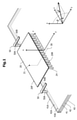
- FIG. 1 is a perspective view of a conductor portion of the antenna device according to the first embodiment.
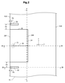
- FIG. 2 is a plan view of the conductor portion of the antenna device according to the first embodiment.
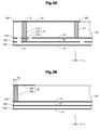
- 3A and 3B are cross-sectional views of the alternate long and short dash line 3A-3A and the alternate long and short dash line 3B-3B of FIG. 2, respectively.
- FIG. 4 is a cross-sectional view taken along the alternate long and short dash line 4-4 of FIG.
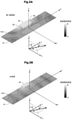
- 5A and 5B are diagrams showing the current distribution at a certain time point of the high frequency current flowing through the ground plane of the antenna device according to the first embodiment and the comparative example, respectively.
- 6A and 6B are graphs showing the angle dependence of the directivity gain of the antenna device according to the first embodiment (FIG.
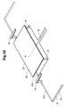
- FIG. 9 is a perspective view of the conductor portion of the antenna device according to the modified example of the first embodiment.
- FIG. 10 is a perspective view of a conductor portion of the antenna device according to another modification of the first embodiment.
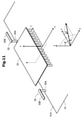
- FIG. 11 is a perspective view of a metal portion of the antenna device according to the second embodiment.
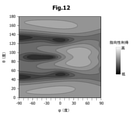
- FIG. 12 is a graph showing the angle dependence of the directivity gain of the antenna device according to the second embodiment by shading.
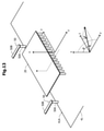
- FIG. 13 is a perspective view of a metal portion of the antenna device according to the third embodiment.
- FIG. 14 is a graph showing the angle dependence of the directivity gain of the antenna device according to the third embodiment by shading.
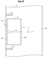
- FIG. 15 is a plan view of the antenna device according to the fourth embodiment.
- FIG. 16 is a perspective view of a metal portion of the antenna device according to the fifth embodiment.
- FIG. 17 is a plan view of the conductor portion of the antenna device according to the sixth embodiment.
- FIG. 18 is a plan view of the antenna device according to the seventh embodiment.
- FIG. 19 is a plan view of the antenna device according to the modified example of the seventh embodiment.
- FIGS. 1 to 8. 1 and 2 are perspective views and plan views of a conductor portion of the antenna device according to the first embodiment, respectively.
- the antenna device according to the first embodiment includes the ground planes 41, 42, 43 of the first layer, the second layer, and the third layer provided on the dielectric substrate, and the radiating element 20.
- the direction from the third layer ground plane 43 to the first layer ground plane 41 is defined as an upward direction.
- Radiating elements 20 are arranged at intervals upward from the ground plane 41 of the first layer.
- the radiating element 20 is composed of a metal plate arranged in parallel with the ground plane 41, and has a rectangular shape in a plan view.
- the edge of the radiating element 20 corresponding to one long side of the rectangle is referred to as the front edge 20F.
- the edge on the opposite side of the front edge 20F is referred to as the rear edge 20R.
- the ground plane 41 has a linear first edge 41A and a second edge 41B (FIG. 2) on the opposite side of the first edge 41A.
- the second-layer ground plane 42 and the third-layer ground plane 43 also have first edges 42A and 43A that correspond to the first edge 41A in a plan view, respectively.
- the radiating element 20 is arranged between the first edge 41A and the second edge 41B of the ground plane 41.
- the front edge 20F of the radiating element 20 overlaps a part of the first edge 41A of the ground plane 41 in a plan view.
- An orthogonal coordinate system is defined in which the direction parallel to the first edge 41A is the z direction, the direction parallel to the first edge 41A is the y direction, and the normal direction of the ground plane 41 is the x direction. do.
- the direction from the first edge 41A to the second edge 41B is defined as the positive direction of the y-axis.
- the direction from the ground plane 41 toward the radiating element 20 is defined as the positive direction of the x-axis.
- the direction from the radiating element 20 is represented by a polar angle ⁇ with respect to the positive direction of the z-axis and an azimuth angle ⁇ with respect to the positive direction of the x-axis in the xy plane.
- the feeder line 30 is connected to the feeder point 21 of the radiation element 20.
- the feeding point 21 is arranged between the midpoint of the front edge 20F and the geometric center of the radiating element 20.
- a high frequency signal is supplied to the radiating element 20 through the feeder line 30.
- the configuration of the feeder line 30 will be described in detail later with reference to FIG. 3A.
- a plurality of short-circuit vias 24 are arranged along the rear edge 20R of the radiating element 20.
- the plurality of short-circuit vias 24 short-circuit the rear edge 20R of the radiating element 20 to the ground plane 41.
- a half patch antenna is configured by the radiating element 20 and the ground plane 41.
- the stubs 50 connected to the ground plane 41 are arranged at positions sandwiching the radiating element 20 in the z direction.
- the stub 50 includes a first portion 50A extending upward (positive direction on the x-axis) from the ground plane 41 and a second portion 50B extending positively on the y-axis from the tip of the first portion 50A.
- the distance in the z direction from the center of the connection point of the stub 50 to the ground plane 41 to the radiating element 20 is referred to as Dz.
- the distance Dz from one stub 50 to the radiating element 20 is equal to the distance Dz from the other stub 50 to the radiating element 20.
- the distance from the center of the connection point of the stub 50 to the ground plane 41 to the first edge 41A of the ground plane 41 is expressed as Dy.
- the second portion 50B of the stub 50 includes a circular pad region sized according to the alignment accuracy in the manufacturing process at the connection point between the first portion 50A and the second portion 50B. This pad region is larger than the first portion 50A in plan view and includes the first portion 50A.
- the pad region included in the second portion 50B is arranged so as to be in contact with the first edge 41A in a plan view. In this case, the total value of the distance between the outer peripheral line of the pad region of the second portion 50B and the outer peripheral line of the first portion 50A and the radius of the first portion 50A is equal to the distance Dy.
- 3A and 3B are cross-sectional views of the alternate long and short dash line 3A-3A and the alternate long and short dash line 3B-3B of FIG. 2, respectively.
- the radiation element 20 and the second portion 50B of the stub 50 are arranged on the upper surface of the dielectric substrate 60, and the third layer ground plane 43 is arranged on the lower surface.
- the first ground plane 41 is arranged on the inner layer of the dielectric substrate 60.
- a second-layer ground plane 42 and a feeder line 30 are arranged between the first-layer ground plane 41 and the third-layer ground plane 43.
- the feeder line 30 is arranged in the same layer as the second layer ground plane 42.
- the feeder line 30 and the ground planes 41 and 43 above and below the feeder line 30 form a strip line having a triplate structure.
- the feeder line 30 is connected to the feeder point 21 of the radiating element 20 via a conductor member 31 extending in the thickness direction of the dielectric substrate 60.
- the conductor member 31 is arranged in the same layer as the ground plane 41 and is separated from the ground plane 41, for example, the inner layer pad 31B, the via 31A connecting the inner layer pad 31B and the feeder line 30, and the inner layer pad 31B and radiation.
- the via 31C connecting the element 20 is included.
- the inner layer pad 31B is slightly larger than the vias 31A and 31C. This difference in size is set according to the alignment accuracy in the manufacturing process.
- the rear edge 20R of the radiating element 20 is short-circuited to the ground plane 41 of the first layer by the short-circuit via 24. A margin depending on the alignment accuracy in the manufacturing process is secured between the connection point of the short-circuit via 24 to the radiating element 20 and the rear edge 20R.
- the front edge 20F of the radiating element 20 and the first edge 41A of the ground plane 41 are arranged at the same position in the y direction.
- the first edges 42A and 43A of the second-layer ground plane 42 and the third-layer ground plane 43 are also arranged at the same positions as the front edge 20F in the y direction.
- the second portion 50B of the stub 50 and the ground plane 41 are connected by the first portion 50A.
- the first portion 50A is arranged slightly inside the first edge 41A of the ground plane 41.
- FIG. 4 is a cross-sectional view taken along the alternate long and short dash line 4-4 of FIG.
- the radiation element 20 is arranged on the upper surface of the dielectric substrate 60, and the ground plane 43 is arranged on the lower surface.
- the radiating element 20 is short-circuited to the inner layer ground plane 41 by a plurality of short-circuit vias 24.
- a ground plane 42 and a feeder line 30 are arranged between the ground planes 41 and 43.
- the distribution of the high frequency current flowing in the ground plane 41 when the radiating element 20 was excited at a frequency corresponding to the resonance frequency of the radiating element 20 was obtained by simulation.
- the resonance frequency of the radiating element 20 is 60 GHz.
- the effective wavelength (hereinafter, may be referred to as an effective wavelength) in consideration of the wavelength shortening effect due to the dielectric constant of the dielectric substrate 60 is about 3.40 mm.
- the "wavelength corresponding to the resonance frequency" means the "effective wavelength corresponding to the resonance frequency”.
- the resonance frequency of the radiating element 20 is determined by the dimension of the radiating element 20 in the y direction, the positional relationship between the radiating element 20 and the first edge 41A of the ground plane 41, the positional relationship between the radiating element 20 and the stub 50, and the like. Radiation.
- FIGS. 5A and 5B are diagrams showing the current distribution at a certain moment of the high frequency current flowing through the ground plane 41 of the antenna device according to the first embodiment and the comparative example, respectively.
- the antenna device according to the comparative example is the same as the antenna device according to the first embodiment in which the stub 50 is removed.
- FIGS. 5A and 5B the region where the surface current density is relatively large is shown in a relatively light color.
- a region having a relatively large surface current density appears periodically in the z direction at the position of the first edge 41A.
- the region having a relatively large surface current density moves in the direction away from the radiating element 20. That is, it was found that a high frequency current propagating along the first edge 41A was generated.
- the antenna device (FIG. 5A) according to the first embodiment, it can be seen that the current is concentrated in the vicinity of the mounting location of the stub 50.
- the high-frequency current generated in the ground plane 41 directly below the radiating element 20 and propagating along the first edge 41A is reflected by the stub 50, so that the propagation of the high-frequency current along the first edge 41A is suppressed.
- FIG. 6A and 6B are graphs showing the angle dependence of the directivity gain of the antenna device according to the first embodiment (FIG. 5A) and the comparative example (FIG. 5B), respectively.
- the horizontal axis represents the azimuth angle ⁇ in the unit “°”, and the vertical axis represents the polar angle ⁇ in the unit “°”.
- the region where the directivity gain is relatively high is shown in a relatively light color.
- the directivity gain is large in the range of the azimuth angle ⁇ of about 45 ° ⁇ 10 ° and the polar angle ⁇ of about 90 ° ⁇ 10 °. That is, the main beam is formed in the direction in which the azimuth angle ⁇ is about 45 ° and the polar angle ⁇ is about 90 °.
- the first embodiment it is possible to suppress secondary radiation from a high-frequency current propagating along the first edge 41A of the ground plane 41 as a wave source. As a result, an excellent effect that the disturbance of the beam pattern can be suppressed can be obtained.
- the distance Dz (FIG. 2) in the z direction from the stub 50 to the radiating element 20 will be described. If the attachment point of the stub 50 to the ground plane 41 is too far from the radiating element 20, the distance that the high frequency current can propagate from the radiating element 20 to the stub 50 becomes long, so that the effect of providing the stub 50 is reduced. .. Further, if the stub 50 is brought too close to the radiating element 20, the ground plane 41 in a region farther than the stub 50 when viewed from the radiating element 20 is coupled to the radiating element 20 to generate a high frequency current. Since the stub 50 is not arranged in the path where the high-frequency current propagates in the direction away from the radiating element 20, the high-frequency current propagates along the first edge 41A. Therefore, it is considered that the distance Dz has a preferable range.
- the horizontal axis represents the distance Dz in the unit " ⁇ m”
- the vertical axis represents the directivity gain in the unit "dBi”.
- the effective wavelength corresponding to the resonance frequency of the radiating element 20 is about 3.40 mm. From the graph shown in FIG. 7, it can be seen that a high directivity gain is obtained by setting the distance Dz to 1/15 or more and 1/4 or less of the effective wavelength.
- the length of the stub 50 corresponds to the total length of the dimension of the first portion 50A in the x direction and the dimension of the second portion 50B in the y direction.
- the horizontal axis represents the length of the stub 50 in the unit " ⁇ m”
- the vertical axis represents the directional gain in the unit "dBi”. It can be seen that a high directivity gain can be obtained by setting the length of the stub 50 in the range of 21% or more and 25% or less of the effective wavelength.
- the distance Dy from the connection point of the stub 50 to the ground plane 41 to the first edge 41A is 1/4 or less of the effective wavelength corresponding to the resonance frequency of the radiating element 20, a high frequency along the first edge 41A. It is considered that a sufficient effect of blocking the propagation of current can be obtained.
- FIG. 9 is a perspective view of the conductor portion of the antenna device according to the modified example of the first embodiment.
- a plurality of short-circuit vias 24 are arranged along the rear edge 20R of the radiating element 20.
- short-circuit vias 24 are arranged at both ends of the rear edge 20R of the radiating element 20.
- the short-circuit via 24 is not arranged at a position other than both ends of the rear edge 20R.
- the radiation element 20 and the ground plane 41 operate as a half patch antenna. In this way, the number and arrangement of the short-circuit vias 24 may be determined under the condition that the radiating element 20 and the ground plane 41 operate as a half patch antenna.
- FIG. 10 is a perspective view of a conductor portion of the antenna device according to another modification of the first embodiment.
- the radiating element 20 is included in the ground plane 41 of the first layer in a plan view.
- the portion of the ground plane 41 (FIG. 1) of the first layer of the antenna device according to the first embodiment that overlaps with the radiating element 20 is removed. Has a shape.
- the first edge 41A of the ground plane 41 does not overlap the front edge 20F of the radiating element 20 in a plan view.
- the extension line of the first edge 41A and the front edge 20F overlap each other in a plan view.
- the feeder line 30 is arranged on the same layer as the second ground plane 42.
- the feeder line 30 is arranged in the same layer as the ground plane 41 of the first layer, and a gap portion from which the metal film is removed is provided between the feeder line 30 and the ground plane 41. It is secured.
- the second layer ground plane 42 includes the radiating element 20 in a plan view. A part of the first edge 42A of the ground plane 42 coincides with the front edge 20F of the radiating element 20 in a plan view.
- the radiating element 20 is short-circuited to the second layer ground plane 42 by short-circuit vias 24 provided at both ends of the rear edge 20R.
- the second layer ground plane 42 is provided on the lower surface of the dielectric substrate, and the third layer ground plane is not provided.
- the vicinity of the end of the first edge 41A of the first layer ground plane 41 close to the radiating element 20 is coupled to the radiating element 20, and the high frequency current propagating along the first edge 41A is generated. Occur.
- the stub 50 suppresses the propagation of high frequency current along the first edge 41A. Further, a high frequency current along the first edge 42A of the second layer ground plane 42 is also generated.
- the stub 50 is also connected to the second layer ground plane 42 at the same location as the connection point with the first layer ground plane 41. Therefore, the stub 50 also suppresses the propagation of high-frequency current along the first edge 42A of the second layer ground plane 42. This makes it possible to suppress the disturbance of the beam pattern.
- the ground plane 41 of the first layer may not overlap with the radiating element 25 in a plan view.
- the radiating element 20 and the ground plane 41 form a half patch antenna, but a normal patch antenna may be formed.
- a normal patch antenna is configured by removing the short-circuit via 24 from the antenna device according to the first embodiment and expanding the dimension of the radiation element 20 in the y direction to twice the dimension of the radiation element 20 of the half patch antenna.
- the shape of the radiating element 20 in a plan view is rectangular, but it may be another shape that can operate as a patch antenna or a half patch antenna.
- the four corners of the rectangle may be cut off into a square shape or a rectangular shape.
- FIG. 11 is a perspective view of a metal portion of the antenna device according to the second embodiment.
- the second portion 50B of the stub 50 extends in the positive direction of the y-axis from the tip of the first portion 50A.
- the second portion 50B of the stub 50 extends from the tip of the first portion 50A in parallel with the first edge 41A and in a direction away from the radiating element 20.
- FIG. 12 is a graph showing the angle dependence of the directivity gain of the antenna device according to the second embodiment by shading.
- the horizontal axis represents the azimuth angle ⁇ in the unit “°”, and the vertical axis represents the polar angle ⁇ in the unit “°”.
- the region where the directivity gain is relatively high is shown in a relatively light color.
- FIG. 13 is a perspective view of a metal portion of the antenna device according to the third embodiment.
- the second portion 50B of the stub 50 extends in the positive direction of the y-axis from the tip of the first portion 50A.
- the second portion 50B of the stub 50 extends from the tip of the first portion 50A in the negative direction of the y-axis.
- FIG. 14 is a graph showing the angle dependence of the directivity gain of the antenna device according to the third embodiment by shading.
- the horizontal axis represents the azimuth angle ⁇ in the unit “°”, and the vertical axis represents the polar angle ⁇ in the unit “°”.
- the region where the directivity gain is relatively high is shown in a relatively light color.
- the extending direction of the second portion 50B (FIGS. 1, 11, and 13) of the stub 50 is not particularly limited.
- the polar angle ⁇ is about 10 ° and about 170 °
- the azimuth angle ⁇ is in the range of ⁇ 70 ° or more and 30 ° or less, which is about the same as the main beam.
- a region of directional gain is generated.
- the third embodiment as shown in FIG. 14, four regions having the same directivity gain as the main beam are generated.
- the input impedance of the antenna device changes.
- the extending direction of the second portion 50B of the stub 50 it becomes possible to achieve impedance matching of the antenna device.
- FIG. 15 is a plan view of the antenna device according to the fourth embodiment.
- the front edge 20F of the radiating element 20 is aligned with a part of the first edge 41A of the ground plane 41 in a plan view.
- the front edge 20F of the radiating element 20 is arranged at a position retracted from the first edge 41A toward the second edge 41B in a plan view.
- the distance in the y direction between the first edge 41A and the front edge 20F is referred to as Gy.
- the distance Gy can also be defined as the distance in the y direction from the first edge 41A to the radiating element 20.
- the distance in the y direction from the rear edge 20R of the radiating element 20 to the second edge 41B of the ground plane 41 is longer than the distance Gy. That is, in a plan view, the radiating element 20 is arranged at a position biased toward the first edge 41A with respect to the ground plane 41.
- the ground plane 41 is coupled to the radiating element 20 and along the first edge 41A. A propagating high frequency current is generated.
- the distance Gy becomes long, the high frequency current propagating along the first edge 41A becomes small, and the beam pattern of the antenna device is hardly disturbed. In this case, it is not necessary to provide the stub 50.
- the distance Gy is 1/4 or less of the effective wavelength corresponding to the resonance frequency of the radiating element 20
- the disturbance of the beam pattern due to the high frequency current propagating along the first edge 41A cannot be ignored. Therefore, when the distance Gy is 1/4 or less of the effective wavelength corresponding to the resonance frequency of the radiating element 20, a significant effect of providing the stub 50 can be obtained.
- FIG. 16 is a perspective view of a metal portion of the antenna device according to the fifth embodiment.
- the radiating element 20 and the ground plane 41 form a half patch antenna.
- the radiating element 20 includes two linear conductors 20A and 20B arranged in parallel with the first edge 41A, and operates as a dipole antenna.
- the other linear conductor 20B is connected to the ground plane 41 via the via 25B, and is further connected to the second layer ground plane 42 via the via 25C arranged directly below the via 25B.
- the vias 25A and 25B are composed of, for example, a plurality of inner layer pads and a plurality of vias connecting the upper and lower inner layer pads to each other.
- the stubs 50 are arranged at positions sandwiching the radiating element 20 in the z direction.
- the configuration of the stub 50 is the same as the configuration of the stub 50 (FIGS. 1 and 3B) of the antenna device according to the first embodiment.
- the distance in the y direction from each of the two linear conductors 20A and 20B to the first edge 41A of the ground plane 41 is the effective wavelength corresponding to the resonance frequency of the radiating element 20 operating as a dipole antenna. It is 1/4 or less.
- the ground plane 41 is coupled to the radiating element 20 operating as a dipole antenna, and a high frequency current propagating along the first edge 41A is generated.
- the stub 50 By suppressing the propagation of the high frequency current along the first edge 41A by the stub 50, the disturbance of the beam pattern can be suppressed.
- FIG. 17 is a plan view of the conductor portion of the antenna device according to the sixth embodiment.
- the antenna device according to the first embodiment has one radiating element 20.
- a plurality of radiating elements 20 having the same structure as the radiating element 20 according to the first embodiment are arranged side by side in the z direction.
- a feeder line 30 is connected to each of the radiating elements 20.
- a common ground plane 41 is arranged for the plurality of radiating elements 20.
- An array antenna is composed of a plurality of radiating elements 20 and a ground plane 41.
- each of the plurality of radiating elements 20 and the first edge 41A of the ground plane 41 is the same as the positional relationship between the radiating element 20 of the antenna device and the first edge 41A of the ground plane 41 according to the first embodiment. ..
- Stubs 50 are arranged on both sides of each of the plurality of radiating elements 20 in the z direction.
- One stub 50 is arranged between two radiating elements 20 adjacent to each other in the z direction, and one stub 50 is shared by the radiating elements 20 on both sides.
- the positional relationship between each of the plurality of radiating elements 20 and the stubs 50 on both sides thereof is the same as the positional relationship between the radiating elements 20 of the antenna device according to the first embodiment and the stubs 50 on both sides thereof.
- the positional relationship between each of the stubs 50 and the first edge 41A of the ground plane 41 is the same as the positional relationship between the stub 50 of the antenna device and the first edge 41A of the ground plane 41 according to the first embodiment.
- the excellent effect of the sixth embodiment will be described.
- the disturbance of each beam pattern of the radiating element 20 can be suppressed as in the first embodiment. Therefore, even in an array antenna including a plurality of radiating elements 20, disturbance of the beam pattern can be suppressed.
- the stubs 50 are individually provided to the radiating elements 20.
- the radiating elements 20 can be arranged closer to each other as compared with the arrangement. Therefore, the degree of freedom in setting the interval of the radiating element 20 is increased.
- FIG. 18 is a plan view of the antenna device according to the seventh embodiment.
- the radiating element 20 is rectangular in a plan view.
- the radiating element 20 is a triangle, for example, an isosceles triangle. The base of the isosceles triangle is parallel to the first edge 41A of the ground plane 41 in a plan view, and corresponds to the rear edge 20R of the radiating element 20.
- the feeding point 21 is arranged on a vertical line extending from the apex 20C to the rear edge 20R.
- the vertex 20C shared by the two equal sides is the closest to the feeding point 21.
- the vertex 20C shared by the two isosceles triangles faces the first edge 41A in a plan view.
- the distance Gy in the y direction from the radiating element 20 to the first edge 41A is equal to the distance in the y direction from the first edge 41A to the apex 20C.
- the distance Dz in the z direction from the center of the connection point of the stub 50 to the ground plane 41 to the radiating element 20 is the apex 20D at both ends of the base of the isosceles triangle and the center of the connection point of the stub 50 to the ground plane 41. Defined by the z-direction spacing between.
- the radiating element 20 operates as a half patch antenna.
- the resonance frequency of the radiating element 20 is determined by the dimension of the radiating element 20 in the y direction, the positional relationship between the radiating element 20 and the first edge 41A of the ground plane 41, the positional relationship between the radiating element 20 and the stub 50, and the like. Will be done.
- the excellent effect of the seventh embodiment will be described.
- the distance Gy is 1/4 or less of the effective wavelength corresponding to the resonance frequency of the radiating element 20
- a significant effect of providing the stub 50 can be obtained. Be done.
- FIG. 19 is a plan view of the antenna device according to the modified example of the seventh embodiment.
- the shape of the radiating element 20 in a plan view is an isosceles triangle, but in this modification, the shape of the radiating element 20 in a plan view is a semicircle.
- the edge corresponding to the semi-circular diameter corresponds to the rear edge 20R.
- the distance Gy in the y direction from the radiating element 20 to the first edge 41A is equal to the distance in the y direction from the intersection 20E between the perpendicular bisector of the rear edge 20R and the circumference to the first edge 41A.
- the feeding point 21 is located on a radius passing through the intersection point 20E.
- the shape of the radiating element 20 in a plan view may be semicircular.
- the shape of the radiating element 20 in a plan view may be a shape obtained by dividing an ellipse into halves with a major axis or a minor axis.
- Radiation element 20A, 20B Linear conductor 20C Apex shared by two equilateral sides of an isosceles triangle Radiation element 20D Apex of both ends of the base of an isosceles triangle radiation element 20E
- Front edge 20R Rear edge 21 Feeding point 24 Short-circuit via 25A, 25B, 25C Via 30
- Conductor member 31A Via 31B Inner layer pad 31C Via 41 Ground plane 41A First edge 41B Second edge 42 Ground Plain 42A 1st edge 43 Ground plane 43A 1st edge 50 stub 50A 1st part of stub 50B 2nd part of stub 60 Dielectric substrate
Landscapes
- Waveguide Aerials (AREA)
- Aerials With Secondary Devices (AREA)
- Variable-Direction Aerials And Aerial Arrays (AREA)
Abstract
Description
第1方向に延びる第1エッジを持つグランドプレーンと、
前記グランドプレーンから前記グランドプレーンの厚さ方向に間隔を隔てて配置された放射素子と、
前記放射素子に高周波信号を供給する給電線と、
前記放射素子を前記第1方向に挟む位置に配置され、前記グランドプレーンに接続された一対のスタブと
を備え、
平面視において、前記放射素子から前記第1エッジまでの、前記第1方向と直交する第2方向の距離が、前記放射素子の共振周波数に対応する波長の1/4以下であるアンテナ装置が提供される。
図1から図8までの図面を参照して、第1実施例によるアンテナ装置について説明する。
図1及び図2は、それぞれ第1実施例によるアンテナ装置の導体部分の斜視図及び平面図である。第1実施例によるアンテナ装置は、誘電体基板に設けられた1層目、2層目、3層目のグランドプレーン41、42、43、及び放射素子20を含む。3層目のグランドプレーン43から1層目のグランドプレーン41に向かう方向を上方向と定義する。
図9は、第1実施例の変形例によるアンテナ装置の導体部分の斜視図である。第1実施例(図1)では、複数の短絡ビア24が放射素子20のリアエッジ20Rに沿って配置されている。これに対して本変形例では、放射素子20のリアエッジ20Rの両端にそれぞれ短絡ビア24が配置されている。リアエッジ20Rの両端以外の箇所には、短絡ビア24が配置されていない。本変形例においても、放射素子20とグランドプレーン41とがハーフパッチアンテナとして動作する。このように、放射素子20とグランドプレーン41とがハーフパッチアンテナとして動作する条件の下で、短絡ビア24の本数及び配置を決定すればよい。
図10は、第1実施例の他の変形例によるアンテナ装置の導体部分の斜視図である。第1実施例(図1)では、平面視において放射素子20が1層目のグランドプレーン41に包含されている。これに対して本変形例によるアンテナ装置の1層目のグランドプレーン41は、第1実施例によるアンテナ装置の1層目のグランドプレーン41(図1)のうち放射素子20と重なる部分が除去された形状を有する。
第1実施例では、放射素子20とグランドプレーン41とでハーフパッチアンテナを構成しているが、通常のパッチアンテナを構成してもよい。第1実施例によるアンテナ装置から短絡ビア24を取り除き、放射素子20のy方向の寸法をハーフパッチアンテナの放射素子20の寸法の2倍に広げることにより、通常のパッチアンテナが構成される。
次に、図11及び図12を参照して第2実施例によるアンテナ装置について説明する。以下、第1実施例によるアンテナ装置(図1から図4までの図面)と共通の構成については説明を省略する。
次に、図13及び図14を参照して第3実施例によるアンテナ装置について説明する。以下、第1実施例によるアンテナ装置(図1から図4までの図面)と共通の構成については説明を省略する。
次に、図15を参照して第4実施例によるアンテナ装置について説明する。以下、第1実施例によるアンテナ装置(図1から図4までの図面)と共通の構成については説明を省略する。
次に、図16を参照して第5実施例によるアンテナ装置について説明する。以下、第1実施例によるアンテナ装置(図1から図4までの図面)と共通の構成については説明を省略する。
第5実施例においても、グランドプレーン41が、ダイポールアンテナとして動作する放射素子20に結合し、第1エッジ41Aに沿って伝搬する高周波電流が発生する。スタブ50が第1エッジ41Aに沿う高周波電流の伝搬を抑制することにより、ビームパターンの乱れを抑制することができる。
次に、図17を参照して第6実施例によるアンテナ装置について説明する。以下、図1から図8までの図面を参照して説明した第1実施例によるアンテナ装置と共通の構成については説明を省略する。
第6実施例においても第1実施例と同様に、放射素子20の各々のビームパターンの乱れを抑制することができる。このため、複数の放射素子20を含むアレイアンテナにおいても、ビームパターンの乱れを抑制することができる。
次に、図18を参照して第7実施例によるアンテナ装置について説明する。以下、第4実施例によるアンテナ装置(図15)と共通の構成については説明を省略する。
第7実施例においても第4実施例と同様に、距離Gyが、放射素子20の共振周波数に対応する実効波長の1/4以下である場合に、スタブ50を設けることの有意な効果が得られる。
図19は、第7実施例の変形例によるアンテナ装置の平面図である。第7実施例では、放射素子20の平面視における形状が二等辺三角形であるが、本変形例では、放射素子20の平面視における形状が半円形である。半円形の直径に対応する縁が、リアエッジ20Rに相当する。
20A、20B 直線状導体
20C 二等辺三角形の放射素子の2つの等辺が共有する頂点
20D 二等辺三角形の放射素子の底辺の両端の頂点
20E 半円形の放射素子のリアエッジの垂直二等分線と円周との交点
20F フロントエッジ
20R リアエッジ
21 給電点
24 短絡ビア
25A、25B、25C ビア
30 給電線
31 導体部材
31A ビア
31B 内層パッド
31C ビア
41 グランドプレーン
41A 第1エッジ
41B 第2エッジ
42 グランドプレーン
42A 第1エッジ
43 グランドプレーン
43A 第1エッジ
50 スタブ
50A スタブの第1部分
50B スタブの第2部分
60 誘電体基板
Claims (8)
- 第1方向に延びる第1エッジを持つグランドプレーンと、
前記グランドプレーンから前記グランドプレーンの厚さ方向に間隔を隔てて配置された少なくとも1つの放射素子と、
前記放射素子に高周波信号を供給する給電線と、
前記放射素子を前記第1方向に挟む位置に配置され、前記グランドプレーンに接続された少なくとも2つのスタブと
を備え、
平面視において、前記放射素子から前記第1エッジまでの、前記第1方向と直交する第2方向の距離が、前記放射素子の共振周波数に対応する波長の1/4以下であるアンテナ装置。 - 前記スタブが前記グランドプレーンに接続されている箇所から前記第1エッジまでの前記第2方向の距離は、前記放射素子の共振周波数に対応する波長の1/4以下である請求項1に記載のアンテナ装置。
- 前記放射素子は、前記グランドプレーンとともにパッチアンテナを構成する金属板を含み、
前記金属板は、平面視において前記第1エッジの側に位置するフロントエッジと、前記フロントエッジの反対側に位置するリアエッジとを有しており、
前記リアエッジから前記グランドプレーンの、前記第1エッジとは反対側の第2エッジまでの前記第2方向の距離が、前記フロントエッジから前記グランドプレーンの前記第1エッジまでの前記第2方向の距離より長い請求項1または2に記載のアンテナ装置。 - 前記スタブが前記グランドプレーンに接続されている箇所から前記放射素子までの前記第1方向の距離が、前記放射素子の共振周波数に対応する波長の1/15以上1/4以下である請求項3に記載のアンテナ装置。
- 前記スタブの各々は、前記グランドプレーンから前記グランドプレーンの厚さ方向に延びる第1部分と、前記第1部分の先端から前記グランドプレーンに対して平行な方向に延びる第2部分とを含む請求項3または4に記載のアンテナ装置。
- 前記スタブの各々の長さが、前記放射素子の共振周波数に対応する波長の21%以上25%以下である請求項3乃至5のいずれか1項に記載のアンテナ装置。
- 前記放射素子は、前記第1方向に沿って複数個配置されており、
前記スタブは、前記放射素子の各々を前記第1方向に挟む位置に配置されており、前記第1方向に隣り合う2つの前記放射素子の間には1つの前記スタブが配置されており、1つの前記スタブが両側の前記放射素子で共用されている請求項1乃至5のいずれか1項に記載のアンテナ装置。 - 前記放射素子は、ダイポールアンテナを構成する2本の直線状導体を含み、前記2本の直線状導体のうち一方は前記給電線に接続されており、他方は前記グランドプレーンに接続されている請求項1または2に記載のアンテナ装置。
Priority Applications (3)
| Application Number | Priority Date | Filing Date | Title |
|---|---|---|---|
| CN202180062616.XA CN116114119B (zh) | 2020-09-15 | 2021-08-25 | 天线装置 |
| JP2022550431A JP7359314B2 (ja) | 2020-09-15 | 2021-08-25 | アンテナ装置 |
| US18/182,410 US12316031B2 (en) | 2020-09-15 | 2023-03-13 | Antenna device |
Applications Claiming Priority (2)
| Application Number | Priority Date | Filing Date | Title |
|---|---|---|---|
| JP2020-155000 | 2020-09-15 | ||
| JP2020155000 | 2020-09-15 |
Related Child Applications (1)
| Application Number | Title | Priority Date | Filing Date |
|---|---|---|---|
| US18/182,410 Continuation US12316031B2 (en) | 2020-09-15 | 2023-03-13 | Antenna device |
Publications (1)
| Publication Number | Publication Date |
|---|---|
| WO2022059445A1 true WO2022059445A1 (ja) | 2022-03-24 |
Family
ID=80776844
Family Applications (1)
| Application Number | Title | Priority Date | Filing Date |
|---|---|---|---|
| PCT/JP2021/031213 Ceased WO2022059445A1 (ja) | 2020-09-15 | 2021-08-25 | アンテナ装置 |
Country Status (4)
| Country | Link |
|---|---|
| US (1) | US12316031B2 (ja) |
| JP (1) | JP7359314B2 (ja) |
| CN (1) | CN116114119B (ja) |
| WO (1) | WO2022059445A1 (ja) |
Citations (4)
| Publication number | Priority date | Publication date | Assignee | Title |
|---|---|---|---|---|
| JP2005203971A (ja) * | 2004-01-14 | 2005-07-28 | Ntt Docomo Inc | アンテナ装置、アンテナシステム |
| EP2323217A1 (en) * | 2009-11-13 | 2011-05-18 | Research In Motion Limited | Antenna for multi mode mimo communication in handheld devices |
| US20140085158A1 (en) * | 2012-09-26 | 2014-03-27 | National Sun Yat-Sen University | Communication device and antennas with high isolation characteristics |
| WO2020100412A1 (ja) * | 2018-11-15 | 2020-05-22 | 株式会社村田製作所 | アンテナモジュール、通信モジュールおよび通信装置 |
Family Cites Families (14)
| Publication number | Priority date | Publication date | Assignee | Title |
|---|---|---|---|---|
| JP4680110B2 (ja) | 2006-03-28 | 2011-05-11 | 京セラ株式会社 | 通信装置 |
| JP4836268B2 (ja) * | 2007-03-06 | 2011-12-14 | 株式会社サムスン横浜研究所 | アンテナ装置 |
| JP4866962B2 (ja) * | 2010-04-22 | 2012-02-01 | アルプス電気株式会社 | アンテナ装置 |
| CN104009292B (zh) * | 2014-06-05 | 2016-10-26 | 太原理工大学 | 小型化宽频微带天线 |
| CN107078405B (zh) * | 2014-10-20 | 2021-03-05 | 株式会社村田制作所 | 无线通信模块 |
| US9865926B2 (en) | 2015-09-02 | 2018-01-09 | Qualcomm Incorporated | Low angle radiating shorted half patch antenna |
| CN205194847U (zh) * | 2015-09-21 | 2016-04-27 | 广东晖速通信技术股份有限公司 | 一种非对称性双极化超宽频振子单元及天线 |
| CN105529530A (zh) * | 2016-01-29 | 2016-04-27 | 杭州电子科技大学 | 双频带低剖面定向天线 |
| CN106229645A (zh) * | 2016-07-19 | 2016-12-14 | 电子科技大学 | 一种双谐振型宽频带偶极子天线 |
| CN107359409B (zh) * | 2017-06-22 | 2019-08-27 | 西安电子科技大学 | 一种应用于基站通信系统的双馈电宽带高增益天线 |
| US11038274B2 (en) * | 2018-01-23 | 2021-06-15 | Samsung Electro-Mechanics Co., Ltd. | Antenna apparatus and antenna module |
| WO2020137375A1 (ja) * | 2018-12-28 | 2020-07-02 | 株式会社村田製作所 | アンテナ装置 |
| CN110212296A (zh) * | 2019-06-17 | 2019-09-06 | 天津大学 | 一种应用于5g毫米波的三维偶极子天线阵元 |
| KR102646542B1 (ko) * | 2019-07-30 | 2024-03-11 | 삼성전기주식회사 | 안테나 장치 |
-
2021
- 2021-08-25 CN CN202180062616.XA patent/CN116114119B/zh active Active
- 2021-08-25 JP JP2022550431A patent/JP7359314B2/ja active Active
- 2021-08-25 WO PCT/JP2021/031213 patent/WO2022059445A1/ja not_active Ceased
-
2023
- 2023-03-13 US US18/182,410 patent/US12316031B2/en active Active
Patent Citations (4)
| Publication number | Priority date | Publication date | Assignee | Title |
|---|---|---|---|---|
| JP2005203971A (ja) * | 2004-01-14 | 2005-07-28 | Ntt Docomo Inc | アンテナ装置、アンテナシステム |
| EP2323217A1 (en) * | 2009-11-13 | 2011-05-18 | Research In Motion Limited | Antenna for multi mode mimo communication in handheld devices |
| US20140085158A1 (en) * | 2012-09-26 | 2014-03-27 | National Sun Yat-Sen University | Communication device and antennas with high isolation characteristics |
| WO2020100412A1 (ja) * | 2018-11-15 | 2020-05-22 | 株式会社村田製作所 | アンテナモジュール、通信モジュールおよび通信装置 |
Also Published As
| Publication number | Publication date |
|---|---|
| CN116114119A (zh) | 2023-05-12 |
| JP7359314B2 (ja) | 2023-10-11 |
| US20230231309A1 (en) | 2023-07-20 |
| CN116114119B (zh) | 2025-10-24 |
| US12316031B2 (en) | 2025-05-27 |
| JPWO2022059445A1 (ja) | 2022-03-24 |
Similar Documents
| Publication | Publication Date | Title |
|---|---|---|
| JP6809576B2 (ja) | アレーアンテナ | |
| JP6073713B2 (ja) | アンテナ装置 | |
| US10886620B2 (en) | Antenna | |
| JPH1075116A (ja) | アンテナ、接続装置、カップラ及び基板積層方法 | |
| US11223132B2 (en) | Antenna device | |
| JP6930441B2 (ja) | アンテナ装置 | |
| JP6189732B2 (ja) | アンテナ装置 | |
| JP6589815B2 (ja) | アンテナ装置 | |
| JPWO2015133114A1 (ja) | アンテナ装置、無線通信装置、及び電子機器 | |
| JP7294248B2 (ja) | アンテナ装置 | |
| JP7359314B2 (ja) | アンテナ装置 | |
| US20200212595A1 (en) | Antenna device | |
| JP3764289B2 (ja) | マイクロストリップアンテナ | |
| US20140368397A1 (en) | Antenna device | |
| JP6913868B2 (ja) | アンテナ装置 | |
| JP6979599B2 (ja) | アンテナ装置 | |
| JP7628982B2 (ja) | ミリ波用の平面アンテナ | |
| JP2005286459A (ja) | アレイアンテナ | |
| WO2019058932A1 (ja) | アンテナ装置 | |
| CN118525420A (zh) | 平面天线 | |
| CN121394905A (zh) | 天线以及天线装置 | |
| WO2015133065A1 (ja) | アンテナ装置、無線通信装置、及び電子機器 | |
| JP2023131594A (ja) | アンテナ装置 | |
| TW202230882A (zh) | 天線模組 |
Legal Events
| Date | Code | Title | Description |
|---|---|---|---|
| 121 | Ep: the epo has been informed by wipo that ep was designated in this application |
Ref document number: 21869132 Country of ref document: EP Kind code of ref document: A1 |
|
| ENP | Entry into the national phase |
Ref document number: 2022550431 Country of ref document: JP Kind code of ref document: A |
|
| NENP | Non-entry into the national phase |
Ref country code: DE |
|
| 122 | Ep: pct application non-entry in european phase |
Ref document number: 21869132 Country of ref document: EP Kind code of ref document: A1 |
|
| WWG | Wipo information: grant in national office |
Ref document number: 202180062616.X Country of ref document: CN |