WO2022054611A1 - レーザー加工装置、及びレーザー加工方法 - Google Patents
レーザー加工装置、及びレーザー加工方法 Download PDFInfo
- Publication number
- WO2022054611A1 WO2022054611A1 PCT/JP2021/031569 JP2021031569W WO2022054611A1 WO 2022054611 A1 WO2022054611 A1 WO 2022054611A1 JP 2021031569 W JP2021031569 W JP 2021031569W WO 2022054611 A1 WO2022054611 A1 WO 2022054611A1
- Authority
- WO
- WIPO (PCT)
- Prior art keywords
- substrate
- main surface
- laser processing
- laser beam
- laser
- Prior art date
- Legal status (The legal status is an assumption and is not a legal conclusion. Google has not performed a legal analysis and makes no representation as to the accuracy of the status listed.)
- Ceased
Links
Images





Classifications
-
- H—ELECTRICITY
- H10—SEMICONDUCTOR DEVICES; ELECTRIC SOLID-STATE DEVICES NOT OTHERWISE PROVIDED FOR
- H10P—GENERIC PROCESSES OR APPARATUS FOR THE MANUFACTURE OR TREATMENT OF DEVICES COVERED BY CLASS H10
- H10P72/00—Handling or holding of wafers, substrates or devices during manufacture or treatment thereof
- H10P72/04—Apparatus for manufacture or treatment
- H10P72/0431—Apparatus for thermal treatment
- H10P72/0436—Apparatus for thermal treatment mainly by radiation
-
- H—ELECTRICITY
- H10—SEMICONDUCTOR DEVICES; ELECTRIC SOLID-STATE DEVICES NOT OTHERWISE PROVIDED FOR
- H10P—GENERIC PROCESSES OR APPARATUS FOR THE MANUFACTURE OR TREATMENT OF DEVICES COVERED BY CLASS H10
- H10P90/00—Preparation of wafers not covered by a single main group of this subclass, e.g. wafer reinforcement
- H10P90/12—Preparing bulk and homogeneous wafers
- H10P90/18—Preparing bulk and homogeneous wafers by shaping
-
- B—PERFORMING OPERATIONS; TRANSPORTING
- B23—MACHINE TOOLS; METAL-WORKING NOT OTHERWISE PROVIDED FOR
- B23K—SOLDERING OR UNSOLDERING; WELDING; CLADDING OR PLATING BY SOLDERING OR WELDING; CUTTING BY APPLYING HEAT LOCALLY, e.g. FLAME CUTTING; WORKING BY LASER BEAM
- B23K26/00—Working by laser beam, e.g. welding, cutting or boring
- B23K26/02—Positioning or observing the workpiece, e.g. with respect to the point of impact; Aligning, aiming or focusing the laser beam
- B23K26/03—Observing, e.g. monitoring, the workpiece
- B23K26/032—Observing, e.g. monitoring, the workpiece using optical means
-
- B—PERFORMING OPERATIONS; TRANSPORTING
- B23—MACHINE TOOLS; METAL-WORKING NOT OTHERWISE PROVIDED FOR
- B23K—SOLDERING OR UNSOLDERING; WELDING; CLADDING OR PLATING BY SOLDERING OR WELDING; CUTTING BY APPLYING HEAT LOCALLY, e.g. FLAME CUTTING; WORKING BY LASER BEAM
- B23K26/00—Working by laser beam, e.g. welding, cutting or boring
- B23K26/02—Positioning or observing the workpiece, e.g. with respect to the point of impact; Aligning, aiming or focusing the laser beam
- B23K26/06—Shaping the laser beam, e.g. by masks or multi-focusing
- B23K26/062—Shaping the laser beam, e.g. by masks or multi-focusing by direct control of the laser beam
- B23K26/0622—Shaping the laser beam, e.g. by masks or multi-focusing by direct control of the laser beam by shaping pulses
-
- B—PERFORMING OPERATIONS; TRANSPORTING
- B23—MACHINE TOOLS; METAL-WORKING NOT OTHERWISE PROVIDED FOR
- B23K—SOLDERING OR UNSOLDERING; WELDING; CLADDING OR PLATING BY SOLDERING OR WELDING; CUTTING BY APPLYING HEAT LOCALLY, e.g. FLAME CUTTING; WORKING BY LASER BEAM
- B23K26/00—Working by laser beam, e.g. welding, cutting or boring
- B23K26/02—Positioning or observing the workpiece, e.g. with respect to the point of impact; Aligning, aiming or focusing the laser beam
- B23K26/06—Shaping the laser beam, e.g. by masks or multi-focusing
- B23K26/073—Shaping the laser spot
-
- B—PERFORMING OPERATIONS; TRANSPORTING
- B23—MACHINE TOOLS; METAL-WORKING NOT OTHERWISE PROVIDED FOR
- B23K—SOLDERING OR UNSOLDERING; WELDING; CLADDING OR PLATING BY SOLDERING OR WELDING; CUTTING BY APPLYING HEAT LOCALLY, e.g. FLAME CUTTING; WORKING BY LASER BEAM
- B23K26/00—Working by laser beam, e.g. welding, cutting or boring
- B23K26/08—Devices involving relative movement between laser beam and workpiece
- B23K26/082—Scanning systems, i.e. devices involving movement of the laser beam relative to the laser head
-
- B—PERFORMING OPERATIONS; TRANSPORTING
- B23—MACHINE TOOLS; METAL-WORKING NOT OTHERWISE PROVIDED FOR
- B23K—SOLDERING OR UNSOLDERING; WELDING; CLADDING OR PLATING BY SOLDERING OR WELDING; CUTTING BY APPLYING HEAT LOCALLY, e.g. FLAME CUTTING; WORKING BY LASER BEAM
- B23K26/00—Working by laser beam, e.g. welding, cutting or boring
- B23K26/36—Removing material
-
- B—PERFORMING OPERATIONS; TRANSPORTING
- B23—MACHINE TOOLS; METAL-WORKING NOT OTHERWISE PROVIDED FOR
- B23K—SOLDERING OR UNSOLDERING; WELDING; CLADDING OR PLATING BY SOLDERING OR WELDING; CUTTING BY APPLYING HEAT LOCALLY, e.g. FLAME CUTTING; WORKING BY LASER BEAM
- B23K26/00—Working by laser beam, e.g. welding, cutting or boring
- B23K26/36—Removing material
- B23K26/361—Removing material for deburring or mechanical trimming
-
- B—PERFORMING OPERATIONS; TRANSPORTING
- B24—GRINDING; POLISHING
- B24B—MACHINES, DEVICES, OR PROCESSES FOR GRINDING OR POLISHING; DRESSING OR CONDITIONING OF ABRADING SURFACES; FEEDING OF GRINDING, POLISHING, OR LAPPING AGENTS
- B24B7/00—Machines or devices designed for grinding plane surfaces on work, including polishing plane glass surfaces; Accessories therefor
- B24B7/20—Machines or devices designed for grinding plane surfaces on work, including polishing plane glass surfaces; Accessories therefor characterised by a special design with respect to properties of the material of non-metallic articles to be ground
- B24B7/22—Machines or devices designed for grinding plane surfaces on work, including polishing plane glass surfaces; Accessories therefor characterised by a special design with respect to properties of the material of non-metallic articles to be ground for grinding inorganic material, e.g. stone, ceramics, porcelain
-
- H—ELECTRICITY
- H10—SEMICONDUCTOR DEVICES; ELECTRIC SOLID-STATE DEVICES NOT OTHERWISE PROVIDED FOR
- H10P—GENERIC PROCESSES OR APPARATUS FOR THE MANUFACTURE OR TREATMENT OF DEVICES COVERED BY CLASS H10
- H10P72/00—Handling or holding of wafers, substrates or devices during manufacture or treatment thereof
- H10P72/04—Apparatus for manufacture or treatment
- H10P72/0451—Apparatus for manufacturing or treating in a plurality of work-stations
- H10P72/0468—Apparatus for manufacturing or treating in a plurality of work-stations comprising a chamber adapted to a particular process
-
- H—ELECTRICITY
- H10—SEMICONDUCTOR DEVICES; ELECTRIC SOLID-STATE DEVICES NOT OTHERWISE PROVIDED FOR
- H10P—GENERIC PROCESSES OR APPARATUS FOR THE MANUFACTURE OR TREATMENT OF DEVICES COVERED BY CLASS H10
- H10P72/00—Handling or holding of wafers, substrates or devices during manufacture or treatment thereof
- H10P72/06—Apparatus for monitoring, sorting, marking, testing or measuring
- H10P72/0616—Monitoring of warpages, curvatures, damages, defects or the like
-
- H—ELECTRICITY
- H10—SEMICONDUCTOR DEVICES; ELECTRIC SOLID-STATE DEVICES NOT OTHERWISE PROVIDED FOR
- H10P—GENERIC PROCESSES OR APPARATUS FOR THE MANUFACTURE OR TREATMENT OF DEVICES COVERED BY CLASS H10
- H10P74/00—Testing or measuring during manufacture or treatment of wafers, substrates or devices
- H10P74/23—Testing or measuring during manufacture or treatment of wafers, substrates or devices characterised by multiple measurements, corrections, marking or sorting processes
-
- H—ELECTRICITY
- H10—SEMICONDUCTOR DEVICES; ELECTRIC SOLID-STATE DEVICES NOT OTHERWISE PROVIDED FOR
- H10P—GENERIC PROCESSES OR APPARATUS FOR THE MANUFACTURE OR TREATMENT OF DEVICES COVERED BY CLASS H10
- H10P90/00—Preparation of wafers not covered by a single main group of this subclass, e.g. wafer reinforcement
- H10P90/12—Preparing bulk and homogeneous wafers
-
- H—ELECTRICITY
- H10—SEMICONDUCTOR DEVICES; ELECTRIC SOLID-STATE DEVICES NOT OTHERWISE PROVIDED FOR
- H10P—GENERIC PROCESSES OR APPARATUS FOR THE MANUFACTURE OR TREATMENT OF DEVICES COVERED BY CLASS H10
- H10P90/00—Preparation of wafers not covered by a single main group of this subclass, e.g. wafer reinforcement
- H10P90/12—Preparing bulk and homogeneous wafers
- H10P90/123—Preparing bulk and homogeneous wafers by grinding or lapping
-
- H—ELECTRICITY
- H10—SEMICONDUCTOR DEVICES; ELECTRIC SOLID-STATE DEVICES NOT OTHERWISE PROVIDED FOR
- H10P—GENERIC PROCESSES OR APPARATUS FOR THE MANUFACTURE OR TREATMENT OF DEVICES COVERED BY CLASS H10
- H10P90/00—Preparation of wafers not covered by a single main group of this subclass, e.g. wafer reinforcement
- H10P90/12—Preparing bulk and homogeneous wafers
- H10P90/126—Preparing bulk and homogeneous wafers by chemical etching
-
- B—PERFORMING OPERATIONS; TRANSPORTING
- B23—MACHINE TOOLS; METAL-WORKING NOT OTHERWISE PROVIDED FOR
- B23K—SOLDERING OR UNSOLDERING; WELDING; CLADDING OR PLATING BY SOLDERING OR WELDING; CUTTING BY APPLYING HEAT LOCALLY, e.g. FLAME CUTTING; WORKING BY LASER BEAM
- B23K2103/00—Materials to be soldered, welded or cut
- B23K2103/50—Inorganic materials other than metals or composite materials
- B23K2103/56—Inorganic materials other than metals or composite materials being semiconducting
-
- H—ELECTRICITY
- H10—SEMICONDUCTOR DEVICES; ELECTRIC SOLID-STATE DEVICES NOT OTHERWISE PROVIDED FOR
- H10P—GENERIC PROCESSES OR APPARATUS FOR THE MANUFACTURE OR TREATMENT OF DEVICES COVERED BY CLASS H10
- H10P74/00—Testing or measuring during manufacture or treatment of wafers, substrates or devices
- H10P74/20—Testing or measuring during manufacture or treatment of wafers, substrates or devices characterised by the properties tested or measured, e.g. structural or electrical properties
- H10P74/203—Structural properties, e.g. testing or measuring thicknesses, line widths, warpage, bond strengths or physical defects
Definitions
- This disclosure relates to a laser processing device and a laser processing method.
- Patent Document 1 describes a method for processing a semiconductor wafer.
- a chamfering step, a wrapping step, an etching step, and a mirror polishing step are performed on a semiconductor wafer obtained by slicing a single crystal ingot.
- One aspect of the present disclosure provides a technique for removing debris adhering to a substrate when slicing a single crystal ingot and suppressing the generation of defects on the substrate due to the debris.
- the laser processing apparatus includes a holding unit, a light source, a moving unit, and a control unit.
- the holding portion holds a substrate which is a slice of a single crystal ingot.
- the light source oscillates a laser beam that irradiates the first main surface of the substrate.
- the moving portion moves the position of the irradiation point of the laser beam on the first main surface of the substrate while the substrate is held by the holding portion.
- the control unit controls the light source and the moving unit to remove the surface layer over the entire first main surface of the substrate.
- debris adhering to the substrate during slicing of a single crystal ingot can be removed, and the generation of defects on the substrate due to the debris can be suppressed.
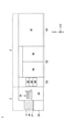
- FIG. 1 is a plan view showing a laser processing apparatus according to an embodiment.
- FIG. 2 is a front view of the laser processing apparatus of FIG.
- FIG. 3A is a side view showing an example of a substrate before laser processing
- FIG. 3B is a side view showing an example of a substrate after laser processing.
- FIG. 4 is a flowchart showing a laser processing method according to an embodiment.
- FIG. 5 is a diagram showing an example of a waviness measuring module.
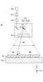
- FIG. 6 is a diagram showing an example of a laser processing module.
- FIG. 7A is a diagram showing a first example of the intensity distribution of the laser beam
- FIG. 7B is a diagram showing a second example of the intensity distribution of the laser beam.
- FIG. 8 (A) is a plan view showing a first example of how to arrange irradiation points
- FIG. 8 (B) is a plan view showing a second example of how to arrange irradiation points
- FIG. 8 (C) is a plan view. It is a top view which shows the 3rd example of how to arrange the irradiation points.
- the same or corresponding configurations may be designated by the same reference numerals and description thereof may be omitted.
- the X-axis direction, the Y-axis direction, and the Z-axis direction are perpendicular to each other.
- the X-axis direction and the Y-axis direction are the horizontal direction, and the Z-axis direction is the vertical direction.
- the laser processing apparatus 1 performs laser processing on the substrate W, which is a slice of a single crystal ingot.
- the substrate W is a silicon wafer or a compound semiconductor wafer.
- the compound semiconductor wafer is not particularly limited, and is, for example, a GaAs wafer, a SiC wafer, a GaN wafer, or an InP wafer.
- the substrate W is a bare wafer.
- the substrate W includes a first main surface Wa and a second main surface Wb opposite to the first main surface Wa.
- the first main surface Wa and the second main surface Wb are formed by slicing a single crystal ingot. During slicing, debris can adhere to the first main surface Wa and the second main surface Wb.
- the debris is, for example, abrasive grains of a cutting blade.
- the laser processing apparatus 1 removes the surface layer Wa1 over the entire first main surface Wa of the substrate W1 and the surface layer Wb1 over the entire second main surface Wb of the substrate W1. To remove. As a result, debris adhering to the substrate W during slicing of the single crystal ingot is removed, and the generation of defects in the substrate W due to the debris is suppressed.
- the laser processing apparatus 1 includes an loading / unloading station 2, a processing station 3, and a control module 9.
- the loading / unloading station 2 and the processing station 3 are arranged side by side in this order in the positive direction of the X-axis.
- the loading / unloading station 2 includes a mounting table 20 and a transport unit 23.
- the mounting table 20 includes a plurality of mounting plates 21.
- the plurality of mounting plates 21 are arranged in a row in the Y-axis direction.
- a cassette C is mounted on each of the plurality (for example, three) mounting plates 21.
- One cassette C accommodates a plurality of unprocessed substrates W.
- the other cassette C accommodates a plurality of processed substrates W.
- the remaining one cassette C accommodates a plurality of substrates W in which an abnormality has occurred during processing.
- the number of mounting plates 21 and the number of cassettes C are not particularly limited.
- the transport unit 23 is arranged adjacent to the X-axis positive direction side of the mounting table 20, and is arranged adjacent to the X-axis negative direction side of the processing station 3.
- the transport unit 23 includes a transport arm 24 that holds the substrate W.
- the transport arm 24 can move in the horizontal direction (both directions in the X-axis direction and the Y-axis direction) and in the vertical direction, and can rotate around the vertical axis.
- the transport arm 24 transports the substrate W between the cassette C on the mounting table 20 and the third processing block G3 of the processing station 3.
- the processing station 3 includes a first processing block G1, a second processing block G2, a third processing block G3, a fourth processing block G4, and a transport block G5.
- the transport block G5 is provided in the area surrounded by the first processing block G1, the second processing block G2, the third processing block G3, and the fourth processing block G4.
- the third processing block G3 is arranged adjacent to the X-axis negative direction side of the transport block G5.
- the transport block G5 includes a transport arm 38 that holds the substrate W.
- the transport arm 38 can move in the horizontal direction (both directions in the X-axis direction and the Y-axis direction) and in the vertical direction, and can rotate around the vertical axis.
- the transport arm 38 transports the substrate W between the first processing block G1, the second processing block G2, the third processing block G3, and the fourth processing block G4.
- the first processing block G1 is arranged adjacent to the Y-axis positive direction side of the transport block G5.
- the first processing block G1 has, for example, a laser processing module 31.
- the laser processing module 31 irradiates the first main surface Wa of the substrate W with a laser beam, and removes the surface layer Wa 1 over the entire first main surface Wa. Further, the laser processing module 31 irradiates the second main surface Wb of the substrate W with a laser beam to remove the surface layer Wb1 over the entire second main surface Wb.
- the surface layers Wa1 and Wb1 absorb a laser beam and change state from a solid phase to a gas phase and scatter, or scatter as a solid phase.
- the second processing block G2 is arranged adjacent to the Y-axis negative direction side of the transport block G5.
- the second processing block G2 has, for example, a cleaning module 32 and an etching module 33.
- the cleaning module 32 scrubs the substrate W and removes debris scattered from the irradiation point of the laser beam from the substrate W.
- the etching module 33 etches the substrate W to reduce the surface roughness of the substrate W, remove the discolored layer by irradiation with a laser beam, and the like. If it is not necessary to remove the debris, the cleaning module 32 is unnecessary. Further, when it is not necessary to reduce the surface roughness or remove the discolored layer, the etching module 33 is unnecessary.
- the arrangement of the cleaning module 32 and the etching module 33 is not limited to the arrangement shown in FIG.
- the third processing block G3 is arranged adjacent to the X-axis negative direction side of the transport block G5.
- the third processing block G3 has, for example, a transition module 34, a waviness measurement module 35, and an inversion module 36.
- the transition module 34 transfers the substrate W between the transfer arm 24 of the loading / unloading station 2 and the transfer arm 38 of the processing station 3.
- the waviness measuring module 35 measures the waviness of the first main surface Wa of the substrate W. Further, the waviness measuring module 35 measures the waviness of the second main surface Wb of the substrate W. A commercially available three-dimensional shape measuring instrument or the like is used for measuring the swell.
- the inversion module 36 inverts the substrate W.
- the arrangement of the transition module 34, the waviness measurement module 35, and the inversion module 36 is not limited to the arrangement shown in FIG.
- the fourth processing block G4 is arranged adjacent to the X-axis positive direction side of the transport block G5.
- the fourth processing block G4 has, for example, a grinding module 37.
- the grinding module 37 grinds the first main surface Wa of the substrate W and improves the flatness of the first main surface Wa. Further, the grinding module 37 grinds the second main surface Wb of the substrate W to improve the flatness of the second main surface Wb. If sufficient flatness can be obtained by irradiation with a laser beam, the grinding module 37 is unnecessary.
- the processing station 3 may have at least a laser processing module 31.
- the types, arrangements, and numbers of modules constituting the processing station 3 are not limited to those shown in FIGS. 1 and 2.
- the control module 9 is, for example, a computer, and includes a CPU (Central Processing Unit) 91 and a storage medium 92 such as a memory.
- the storage medium 92 stores programs that control various processes executed by the laser processing apparatus 1.
- the control module 9 controls the operation of the laser processing device 1 by causing the CPU 91 to execute the program stored in the storage medium 92.
- Steps S101 to S109 shown in FIG. 4 are carried out under the control of the control module 9.
- the transport arm 24 of the loading / unloading station 2 takes out the substrate W from the cassette C on the mounting table 20 and transports it to the transition module 34.
- the transfer arm 38 of the processing station 3 receives the substrate W from the transition module 34 and transfers it to the waviness measurement module 35. During this time, the substrate W is held horizontally with the first main surface Wa facing up.
- the waviness measurement module 35 measures the waviness of the first main surface Wa of the substrate W (step S101).
- the measurement of swell is performed in a natural state where external force other than gravity and its drag force, for example, adsorption force does not work.
- the natural state is a state in which the substrate W is not deformed, and the stress on the surface of the substrate is substantially zero.
- the waviness measurement is performed with the substrate W simply placed on the horizontal plane of the stage 35a, as shown in FIG.
- the waviness measuring module 35 has a displacement meter 35b.
- the displacement meter 35b measures the height distribution of the upper surface (for example, the first main surface Wa) of the substrate W.
- the displacement meter 35b is a non-contact type in this embodiment, but may be a contact type.
- the waviness measurement module 35 transmits the measurement data to the control module 9. After the step S101, the transfer arm 38 takes out the substrate W from the waviness measurement module 35 and transfers it to the laser processing module 31.
- the laser processing module 31 performs laser processing on the first main surface Wa of the substrate W (step S102). As shown in FIG. 6, the laser processing module 31 irradiates the first main surface Wa with the laser beam LB, and moves the position of the irradiation point P over the entire first main surface Wa. The surface layer Wa1 is removed over the entire first main surface Wa.
- Debris adheres to the surface layer Wa1 when slicing a single crystal ingot. If the substrate W is ground (including polishing) with the debris attached, the debris is pressed against the substrate W and a defect is generated in the substrate W. The resulting defects can be expanded by subsequent etching.
- the debris adhering to the surface layer Wa1 can be removed. Further, since the surface layer Wa1 is removed, debris that cannot be removed by brush cleaning or the like can be removed. Therefore, it is possible to suppress the occurrence of defects in the substrate W due to debris.
- the laser processing module 31 may reduce the waviness of the first main surface Wa when removing the surface layer Wa1.
- the amount of removal is controlled by the integrated irradiation amount (unit: J), which is the product of the output of the laser beam LB (unit: W) and the irradiation time. The larger the cumulative irradiation amount, the larger the removal amount.
- the control module 9 refers to the measurement data of the waviness measurement module 35 and controls the integrated irradiation amount of the laser beam LB per unit area of the first main surface Wa so as to reduce the waviness of the first main surface Wa.
- the control includes one or more selected from the control of the output of the light source 31b and the control of the irradiation time.
- the substrate W If the substrate W is pressed against the surface plate and polished in order to reduce the waviness of the first main surface Wa, the substrate W will be elastically deformed. Therefore, it is difficult to reduce the waviness of the substrate W. Further, the debris is pressed against the substrate W, causing a defect in the substrate W.
- control module 9 controls the integrated irradiation amount per unit area with reference to the measurement data of the swell of the first main surface Wa in the natural state, so that the swell can be efficiently reduced. It can be efficiently straightened to a flat surface.
- Laser processing of the first main surface Wa is performed in a natural state, for example, the substrate W is simply placed on the horizontal plane of the stage 31a. Even if a foreign substance exists between the substrate W and the stage 31a, the foreign substance is not pressed against the substrate W, so that the substrate W does not have a defect.
- the laser processing of the first main surface Wa may be performed in a state of being adsorbed on the horizontal plane of the stage 31a, unlike the measurement of the waviness. Since the amount of surface layer Wa1 removed is determined by the integrated irradiation amount, it is possible to reduce the swell. Further, the displacement of the substrate W can be prevented by adsorption.
- the transfer arm 38 takes out the substrate W from the laser processing module 31 and transfers it to the cleaning module 32.
- the cleaning module 32 scrubs the substrate W (step S103) and removes debris scattered from the irradiation point P of the laser beam LB from the substrate W.
- the transfer arm 38 takes out the substrate W from the cleaning module 32 and transfers it to the reversing module 36.
- the inversion module 36 inverts the substrate W (step S104) and turns the second main surface Wb of the substrate W upward.
- the transfer arm 38 takes out the substrate W from the reversing module 36 and transfers it to the waviness measurement module 35 again. During this time, the substrate W is held horizontally with the second main surface Wb facing up.
- the waviness measuring module 35 measures the waviness of the second main surface Wb of the substrate W (step S105).
- the measurement of the swell is performed in a natural state, for example, in a state where the substrate W is simply placed on the horizontal plane of the stage 35a.
- the displacement meter 35b measures the height distribution of the second main surface Wb of the substrate W.
- the waviness measurement module 35 transmits the measurement data to the control module 9.
- the transfer arm 38 takes out the substrate W from the waviness measurement module 35 and transfers it to the laser processing module 31 again.
- the laser processing module 31 performs laser processing on the second main surface Wb of the substrate W (step S106). Specifically, the laser processing module 31 irradiates the second main surface Wb with the laser beam LB, moves the position of the irradiation point P over the entire second main surface Wb, and causes the entire second main surface Wb. The surface layer Wb1 is removed.
- the debris adhering to the surface layer Wb1 can be removed. Further, since the surface layer Wb1 is removed, debris that cannot be removed by brush cleaning or the like can be removed. Therefore, it is possible to suppress the occurrence of defects in the substrate W due to debris.
- the laser processing module 31 may reduce the waviness of the second main surface Wb when the surface layer Wb1 is removed.
- the amount of removal is controlled by the integrated irradiation amount (unit: J), which is the product of the output of the laser beam LB (unit: W) and the irradiation time. The larger the cumulative irradiation amount, the larger the removal amount.
- the control module 9 refers to the measurement data of the waviness measurement module 35 and controls the integrated irradiation amount of the laser beam LB per unit area of the second main surface Wb so as to reduce the waviness of the second main surface Wb.
- the control includes one or more selected from the control of the output of the light source 31b and the control of the irradiation time.
- control module 9 controls the integrated irradiation amount per unit area with reference to the measurement data of the swell of the second main surface Wb in the natural state, so that the swell can be efficiently reduced. It can be efficiently straightened to a flat surface.
- Laser processing of the second main surface Wb is performed in a natural state, for example, the substrate W is simply placed on the horizontal plane of the stage 31a. Even if a foreign substance exists between the substrate W and the stage 31a, the foreign substance is not pressed against the substrate W, so that the substrate W does not have a defect.
- the laser processing of the second main surface Wb may be performed in a state of being adsorbed on the horizontal plane of the stage 31a, unlike the measurement of the waviness. Since the amount of surface layer Wb1 removed is determined by the integrated irradiation amount, it is possible to reduce the swell. Further, the displacement of the substrate W can be prevented by adsorption.
- the transfer arm 38 takes out the substrate W from the laser processing module 31 and transfers it to the cleaning module 32 again.
- the cleaning module 32 scrubs the substrate W (step S107) and removes debris scattered from the irradiation point P of the laser beam LB from the substrate W.
- the transport arm 38 takes out the substrate W from the cleaning module 32 and transports it to the etching module 33.
- the etching module 33 etches the substrate W (step S108), reduces the surface roughness of the substrate W, removes the discolored layer by irradiation with a laser beam, and the like.
- the etching module 33 wet-etches the substrate W, for example, and simultaneously etches the first main surface Wa and the second main surface Wb of the substrate W.
- the etching module 33 may dry-etch the substrate W, or may sequentially etch the first main surface Wa and the second main surface Wb of the substrate W.
- the transfer arm 38 takes out the substrate W from the etching module 33 and transfers it to the grinding module 37.
- the grinding module 37 grinds the substrate W (step S109) to improve the flatness of the substrate W.
- the grinding module 37 grinds the first main surface Wa of the substrate W and improves the flatness of the first main surface Wa.
- the grinding module 37 may grind the second main surface Wb of the substrate W, or may improve the flatness of the second main surface Wb. Grinding of the first main surface Wa and grinding of the second main surface Wb are performed in order, and the substrate W is inverted in the middle.
- grinding includes polishing.
- the order of grinding the substrate W (step S109) and etching the substrate W (S108) may be reversed.
- the substrate W may be ground, subsequently both sides of the substrate W may be cleaned, and then the substrate W may be etched.
- the etching may be double-sided etching or single-sided etching.
- the transfer arm 38 takes out the substrate W from the grinding module 37 and transfers it to the transition module 34.
- the transfer arm 24 of the loading / unloading station 2 takes out the substrate W from the transition module 34 and accommodates the substrate W in the cassette C on the mounting table 20.
- the laser processing module 31 includes, for example, a stage 31a which is a holding portion, a light source 31b, and a galvano scanner 31c which is a moving portion. Further, the laser processing module 31 includes an f ⁇ lens 31d, a homogenizer 31e, and an aperture 31f.
- the stage 31a holds the substrate W.
- the stage 31a holds the substrate W horizontally from below with the main surface of the substrate W irradiating the laser beam LB facing upward.
- the stage 31a holds the substrate W in a natural state without adsorbing it.
- the stage 31a of the present embodiment does not adsorb the substrate W, it may be adsorbed. In the latter case, the stage 31a is a vacuum chuck or an electrostatic chuck.
- the light source 31b oscillates a laser beam LB that irradiates the upper surface of the substrate W (for example, the first main surface Wa).
- the laser beam LB has an absorbency with respect to the substrate W.
- the laser beam LB is, for example, UV light.
- the substrate W absorbs the laser beam LB and changes its state from the solid phase to the gas phase and scatters, or scatters in the solid phase.
- the surface layer Wa1 of the first main surface Wa of the substrate W is removed.
- the laser beam LB may be focused and irradiated on the upper surface of the substrate W.
- the irradiation point P is a focusing point having the highest power density in the present embodiment. However, the irradiation point P does not have to be a condensing point.
- the light source 31b is, for example, a pulse laser.
- the irradiation time per pulse is, for example, 30 nsec or less. If the irradiation time per pulse is 30 nsec or less, the substrate W can be irradiated with a laser beam LB having a high power density in a short time, and overheating of the substrate W can be suppressed. Therefore, deterioration of the substrate W due to heat can be suppressed, and for example, the generation of a discolored layer can be suppressed.
- the irradiation time per pulse is preferably 10 psec or less. If the irradiation time per pulse is 10 psec or less, even if the irradiation points P are formed at the same location a plurality of times, the deterioration of the substrate W due to heat can be suppressed.
- the galvano scanner 31c is arranged above the substrate W held by the stage 31a, for example. According to the galvano scanner 31c, the position of the irradiation point P of the laser beam LB on the upper surface of the substrate W can be moved without moving the stage 31a. Even if the stage 31a does not adsorb the substrate W, if the stage 31a does not move, the position of the substrate W with respect to the stage 31a does not shift. Therefore, the position of the irradiation point P can be controlled with high accuracy.
- the galvano scanner 31c includes two sets of a galvano mirror 31c1 and a galvano motor 31c2 (only one set is shown in FIG. 6).
- One galvano motor 31c2 rotates one galvano mirror 31c1 to displace the irradiation point P in the X-axis direction.
- Another galvano motor 31c2 rotates another galvano mirror 31c1 to displace the irradiation point P in the Y-axis direction.
- the moving part of the present embodiment is a galvano scanner 31c, but the technique of the present disclosure is not limited to this.
- the moving unit may include a polygon scanner instead of the galvano scanner 31c.
- the scanning speed is faster than that of the galvano scanner 31c, and a high frequency pulse laser can be used.
- the moving portion may be any as long as it moves the position of the irradiation point P of the laser beam LB on the first main surface Wa of the substrate W while holding the substrate W on the stage 31a.
- the moving portion may be one that moves the stage 31a in the X-axis direction and the Y-axis direction, or may have a motor and a ball screw mechanism that converts the rotational motion of the motor into the linear motion of the stage 31a. good. Further, the moving portion may have a mechanism for rotating the stage 31a around the vertical axis.
- the f ⁇ lens 31d forms a focal plane perpendicular to the Z-axis direction. While the galvano scanner 31c moves the position of the irradiation point P in the X-axis direction or the Y-axis direction, the f ⁇ lens 31d maintains the Z-axis direction position of the irradiation point P on the focal plane, and the irradiation point P on the focal plane Maintain shape and dimensions. As a result, as will be described later, the rectangular irradiation points P can be regularly and two-dimensionally arranged on the upper surface of the substrate W without any gaps. The height of the irradiation point P is the height of the focal plane.
- the homogenizer 31e converts the intensity distribution of the laser beam LB from the Gaussian distribution shown in FIG. 7 (A) to the top hat distribution shown in FIG. 7 (B), and homogenizes the intensity distribution.
- the aperture 31f shapes the cross-sectional shape of the laser beam LB into a rectangular shape.
- the rectangle includes not only a rectangle but also a square.
- the aperture 31f is a light-shielding film having a rectangular opening. The opening allows, for example, the laser beam LB in the range indicated by the arrow D in FIG. 7 (B) to pass through.
- the homogenizer 31e and the aperture 31f can form a rectangular irradiation point P having a uniform intensity distribution.
- the integrated irradiation amount of the laser beam LB per unit area can be controlled with high accuracy.
- the irradiation point P is a rectangle having a uniform intensity distribution, the two sides of the rectangle are parallel to the X-axis direction, and the remaining two sides of the rectangle are parallel to the Y-axis direction. ..
- the X-axis direction dimension X0 of the irradiation point P may be the same as or different from the Y-axis direction dimension Y0 of the irradiation point P. The same applies to FIGS. 8 (B) and 8 (C).
- the control module 9 moves the irradiation point P by X0 in the X-axis direction during the off-time of the pulse while oscillating the laser beam LB in a pulse manner, and moves the irradiation point P in the X-axis direction in the X-axis direction.
- Irradiation points P are arranged in a row without gaps over the entire area.
- the control module 9 moves the irradiation point P in the Y-axis direction by Y0 during the pulse off time while oscillating the laser beam LB in a pulse, and moves the irradiation point P in the X-axis direction during the pulse off time.
- the irradiation points P are arranged two-dimensionally without a gap over the entire upper surface of the substrate W by repeating the movement of X0 at a time.
- the control module 9 moves the irradiation point P in the X-axis direction by half the value of X0 while oscillating the laser beam LB while oscillating the pulse, and the upper surface of the substrate W.
- the irradiation points P are overlapped and arranged in a row over the entire X-axis direction.
- the control module 9 moves the irradiation point P in the Y-axis direction by Y0 during the pulse off time while oscillating the laser beam LB in a pulse, and moves the irradiation point P in the X-axis direction during the pulse off time.
- the irradiation points P are arranged two-dimensionally without a gap over the entire upper surface of the substrate W by repeating the process of moving by half the value of X0.
- the control module 9 oscillates the laser beam LB while oscillating the pulse, and instead of moving the irradiation point P by Y0 in the Y-axis direction during the pulse off time, the control module 9 sets the irradiation point P to Y during the pulse off time. It may be carried out to move by half the value of Y0 in the axial direction.
- the control module 9 moves the irradiation point P in the X-axis direction twice as much as X0 in the X-axis direction while oscillating the laser beam LB while oscillating the pulse, and the substrate W. Irradiation points P are arranged in a row while forming a gap SP over the entire X-axis direction of the upper surface.
- the control module 9 moves the irradiation point P twice in the X-axis direction during the off time of the pulse while oscillating the laser beam LB again so as to fill the gap SP with the irradiation point P.
- the control module 9 moves the irradiation point P in the Y-axis direction by Y0 during the pulse off time while oscillating the laser beam LB in a pulse, and moves the irradiation point P in the X-axis direction during the pulse off time.
- the irradiation point P is moved twice as much as X0 and the irradiation point P is moved twice as much as X0 in the X-axis direction during the pulse off time so as to fill the gap SP with the irradiation point P.
- Ps are arranged two-dimensionally without any gaps.
- the waviness measurement module 35 and the inversion module 36 are provided separately from the laser processing module 31, but the technique of the present disclosure is not limited to this.
- the laser processing module 31 may have the function of the waviness measurement module 35. Further, the laser processing module 31 may have the function of the reversing module 36.
- Control module (control unit) 31 Laser processing module 31a Stage (holding part) 31b Light source 31c Moving part (galvano scanner)
Landscapes
- Engineering & Computer Science (AREA)
- Optics & Photonics (AREA)
- Physics & Mathematics (AREA)
- Mechanical Engineering (AREA)
- Plasma & Fusion (AREA)
- Chemical & Material Sciences (AREA)
- Inorganic Chemistry (AREA)
- Ceramic Engineering (AREA)
- Laser Beam Processing (AREA)
- Mechanical Treatment Of Semiconductor (AREA)
- Health & Medical Sciences (AREA)
- Toxicology (AREA)
- Chemical Kinetics & Catalysis (AREA)
- General Chemical & Material Sciences (AREA)
Priority Applications (3)
| Application Number | Priority Date | Filing Date | Title |
|---|---|---|---|
| JP2022547504A JP7483020B2 (ja) | 2020-09-09 | 2021-08-27 | レーザー加工装置、及びレーザー加工方法 |
| US18/044,386 US20240030021A1 (en) | 2020-09-09 | 2021-08-27 | Laser processing apparatus and laser processing method |
| JP2024073839A JP7765158B2 (ja) | 2020-09-09 | 2024-04-30 | レーザー加工装置、及びレーザー加工方法 |
Applications Claiming Priority (2)
| Application Number | Priority Date | Filing Date | Title |
|---|---|---|---|
| JP2020-151606 | 2020-09-09 | ||
| JP2020151606 | 2020-09-09 |
Publications (1)
| Publication Number | Publication Date |
|---|---|
| WO2022054611A1 true WO2022054611A1 (ja) | 2022-03-17 |
Family
ID=80631646
Family Applications (1)
| Application Number | Title | Priority Date | Filing Date |
|---|---|---|---|
| PCT/JP2021/031569 Ceased WO2022054611A1 (ja) | 2020-09-09 | 2021-08-27 | レーザー加工装置、及びレーザー加工方法 |
Country Status (4)
| Country | Link |
|---|---|
| US (1) | US20240030021A1 (https=) |
| JP (2) | JP7483020B2 (https=) |
| TW (1) | TWI904225B (https=) |
| WO (1) | WO2022054611A1 (https=) |
Cited By (5)
| Publication number | Priority date | Publication date | Assignee | Title |
|---|---|---|---|---|
| WO2024210048A1 (ja) * | 2023-04-07 | 2024-10-10 | 東京エレクトロン株式会社 | 基板処理方法および基板処理装置 |
| WO2024210026A1 (ja) * | 2023-04-07 | 2024-10-10 | 東京エレクトロン株式会社 | 基板処理方法および基板処理装置 |
| WO2024209992A1 (ja) * | 2023-04-07 | 2024-10-10 | 東京エレクトロン株式会社 | 基板処理方法および基板処理装置 |
| WO2025041188A1 (ja) * | 2023-08-18 | 2025-02-27 | 株式会社ニコン | 加工システム、計測装置及び加工方法 |
| WO2025094667A1 (ja) * | 2023-11-02 | 2025-05-08 | 東京エレクトロン株式会社 | 基板処理装置及び基板処理方法 |
Families Citing this family (1)
| Publication number | Priority date | Publication date | Assignee | Title |
|---|---|---|---|---|
| WO2025258398A1 (ja) * | 2024-06-11 | 2025-12-18 | 東京エレクトロン株式会社 | 基板処理方法および基板処理装置 |
Citations (5)
| Publication number | Priority date | Publication date | Assignee | Title |
|---|---|---|---|---|
| JPH1167777A (ja) * | 1997-08-19 | 1999-03-09 | Hamamatsu Photonics Kk | 半導体ウェハの製造方法 |
| JPH1167700A (ja) * | 1997-08-22 | 1999-03-09 | Hamamatsu Photonics Kk | 半導体ウェハの製造方法 |
| JP2007014990A (ja) * | 2005-07-07 | 2007-01-25 | Aisin Seiki Co Ltd | レーザ加工方法及びレーザ加工装置 |
| JP2014091133A (ja) * | 2012-10-31 | 2014-05-19 | Mitsubishi Heavy Ind Ltd | レーザ溶断装置および加工方法 |
| JP2015199173A (ja) * | 2014-04-09 | 2015-11-12 | 株式会社ディスコ | 研削装置 |
Family Cites Families (14)
| Publication number | Priority date | Publication date | Assignee | Title |
|---|---|---|---|---|
| US5504303A (en) * | 1994-12-12 | 1996-04-02 | Saint-Gobain/Norton Industrial Ceramics Corp. | Laser finishing and measurement of diamond surface roughness |
| JPH09199454A (ja) * | 1996-01-16 | 1997-07-31 | Toyoda Mach Works Ltd | シリコンウエハ加工方法および加工装置 |
| JP3943869B2 (ja) * | 2000-06-29 | 2007-07-11 | 信越半導体株式会社 | 半導体ウエーハの加工方法および半導体ウエーハ |
| JP2002329690A (ja) | 2001-04-27 | 2002-11-15 | Sumitomo Mitsubishi Silicon Corp | 半導体ウェーハの製造方法 |
| JP2003045828A (ja) | 2001-08-01 | 2003-02-14 | Sony Corp | 半導体処理方法および処理装置 |
| TW201101377A (en) * | 2009-06-19 | 2011-01-01 | Shu-Ling Guo | Manufacturing method for semiconductor integrated circuit wafer |
| JP5735260B2 (ja) * | 2010-11-10 | 2015-06-17 | 株式会社ディスコ | サファイア基板の加工方法 |
| JP2014167996A (ja) * | 2013-02-28 | 2014-09-11 | Ebara Corp | 研磨装置および研磨方法 |
| JP6631888B2 (ja) * | 2015-02-07 | 2020-01-15 | 株式会社クリエイティブテクノロジー | 被加工物保持装置及びレーザカット加工方法 |
| US20180126485A1 (en) | 2016-11-10 | 2018-05-10 | Goodrich Corporation | Surface finishing for glass components using a laser |
| CN107452607A (zh) * | 2017-08-02 | 2017-12-08 | 武汉大学 | 一种晶圆激光研磨系统及方法 |
| WO2019220666A1 (ja) | 2018-05-17 | 2019-11-21 | 信越エンジニアリング株式会社 | ワーク分離装置及びワーク分離方法 |
| JP7133633B2 (ja) | 2018-09-13 | 2022-09-08 | 東京エレクトロン株式会社 | 処理システム及び処理方法 |
| CN109693039B (zh) * | 2018-12-27 | 2021-07-16 | 北京航空航天大学 | 一种硅片表面激光抛光的方法 |
-
2021
- 2021-08-27 WO PCT/JP2021/031569 patent/WO2022054611A1/ja not_active Ceased
- 2021-08-27 JP JP2022547504A patent/JP7483020B2/ja active Active
- 2021-08-27 US US18/044,386 patent/US20240030021A1/en active Pending
- 2021-08-30 TW TW110131980A patent/TWI904225B/zh active
-
2024
- 2024-04-30 JP JP2024073839A patent/JP7765158B2/ja active Active
Patent Citations (5)
| Publication number | Priority date | Publication date | Assignee | Title |
|---|---|---|---|---|
| JPH1167777A (ja) * | 1997-08-19 | 1999-03-09 | Hamamatsu Photonics Kk | 半導体ウェハの製造方法 |
| JPH1167700A (ja) * | 1997-08-22 | 1999-03-09 | Hamamatsu Photonics Kk | 半導体ウェハの製造方法 |
| JP2007014990A (ja) * | 2005-07-07 | 2007-01-25 | Aisin Seiki Co Ltd | レーザ加工方法及びレーザ加工装置 |
| JP2014091133A (ja) * | 2012-10-31 | 2014-05-19 | Mitsubishi Heavy Ind Ltd | レーザ溶断装置および加工方法 |
| JP2015199173A (ja) * | 2014-04-09 | 2015-11-12 | 株式会社ディスコ | 研削装置 |
Cited By (5)
| Publication number | Priority date | Publication date | Assignee | Title |
|---|---|---|---|---|
| WO2024210048A1 (ja) * | 2023-04-07 | 2024-10-10 | 東京エレクトロン株式会社 | 基板処理方法および基板処理装置 |
| WO2024210026A1 (ja) * | 2023-04-07 | 2024-10-10 | 東京エレクトロン株式会社 | 基板処理方法および基板処理装置 |
| WO2024209992A1 (ja) * | 2023-04-07 | 2024-10-10 | 東京エレクトロン株式会社 | 基板処理方法および基板処理装置 |
| WO2025041188A1 (ja) * | 2023-08-18 | 2025-02-27 | 株式会社ニコン | 加工システム、計測装置及び加工方法 |
| WO2025094667A1 (ja) * | 2023-11-02 | 2025-05-08 | 東京エレクトロン株式会社 | 基板処理装置及び基板処理方法 |
Also Published As
| Publication number | Publication date |
|---|---|
| JP7483020B2 (ja) | 2024-05-14 |
| JPWO2022054611A1 (https=) | 2022-03-17 |
| TW202216337A (zh) | 2022-05-01 |
| JP7765158B2 (ja) | 2025-11-06 |
| TWI904225B (zh) | 2025-11-11 |
| US20240030021A1 (en) | 2024-01-25 |
| JP2024097842A (ja) | 2024-07-19 |
Similar Documents
| Publication | Publication Date | Title |
|---|---|---|
| JP7483020B2 (ja) | レーザー加工装置、及びレーザー加工方法 | |
| JP7655651B2 (ja) | 基板加工方法、及び基板加工装置 | |
| JP7118245B2 (ja) | 基板処理システム、および基板処理方法 | |
| JP7347939B2 (ja) | シリコンウェハの表面の研削修復装置及び研削修復方法 | |
| US20190039185A1 (en) | Laser processing apparatus | |
| JP7359980B2 (ja) | シリコンウェハの研削後表面のレーザー照射修復装置及び修復方法 | |
| JP5453123B2 (ja) | 切削方法 | |
| WO2024210026A1 (ja) | 基板処理方法および基板処理装置 | |
| WO2019239801A1 (ja) | 基板処理システム、および基板処理方法 | |
| TW202604664A (zh) | 雷射加工裝置及雷射加工方法 | |
| JP7685345B2 (ja) | ウェーハのテラス加工方法及びそれに用いる加工装置 | |
| JP7802178B2 (ja) | 基板処理方法、および基板処理装置 | |
| WO2024210048A1 (ja) | 基板処理方法および基板処理装置 | |
| WO2024209992A1 (ja) | 基板処理方法および基板処理装置 | |
| JPH1167777A (ja) | 半導体ウェハの製造方法 | |
| WO2025258398A1 (ja) | 基板処理方法および基板処理装置 | |
| WO2025047207A1 (ja) | 基板処理方法および基板処理システム | |
| JP2026007509A (ja) | ウェーハの製造方法、レーザー加工装置、及びウェーハ製造装置 | |
| JP2024031439A (ja) | ウェーハの分割方法 |
Legal Events
| Date | Code | Title | Description |
|---|---|---|---|
| 121 | Ep: the epo has been informed by wipo that ep was designated in this application |
Ref document number: 21866570 Country of ref document: EP Kind code of ref document: A1 |
|
| ENP | Entry into the national phase |
Ref document number: 2022547504 Country of ref document: JP Kind code of ref document: A |
|
| WWE | Wipo information: entry into national phase |
Ref document number: 18044386 Country of ref document: US |
|
| NENP | Non-entry into the national phase |
Ref country code: DE |
|
| 122 | Ep: pct application non-entry in european phase |
Ref document number: 21866570 Country of ref document: EP Kind code of ref document: A1 |