WO2022030645A1 - 銅張積層体及びその製造方法 - Google Patents
銅張積層体及びその製造方法 Download PDFInfo
- Publication number
- WO2022030645A1 WO2022030645A1 PCT/JP2021/029462 JP2021029462W WO2022030645A1 WO 2022030645 A1 WO2022030645 A1 WO 2022030645A1 JP 2021029462 W JP2021029462 W JP 2021029462W WO 2022030645 A1 WO2022030645 A1 WO 2022030645A1
- Authority
- WO
- WIPO (PCT)
- Prior art keywords
- plating layer
- copper plating
- resin film
- clad laminate
- electroless copper
- Prior art date
- Legal status (The legal status is an assumption and is not a legal conclusion. Google has not performed a legal analysis and makes no representation as to the accuracy of the status listed.)
- Ceased
Links
- 0 *[N+](C1=CC=IC=C1)[O-] Chemical compound *[N+](C1=CC=IC=C1)[O-] 0.000 description 1
Images






Classifications
-
- H—ELECTRICITY
- H05—ELECTRIC TECHNIQUES NOT OTHERWISE PROVIDED FOR
- H05K—PRINTED CIRCUITS; CASINGS OR CONSTRUCTIONAL DETAILS OF ELECTRIC APPARATUS; MANUFACTURE OF ASSEMBLAGES OF ELECTRICAL COMPONENTS
- H05K3/00—Apparatus or processes for manufacturing printed circuits
- H05K3/38—Improvement of the adhesion between the insulating substrate and the metal
- H05K3/388—Improvement of the adhesion between the insulating substrate and the metal by the use of a metallic or inorganic thin film adhesion layer
-
- C—CHEMISTRY; METALLURGY
- C23—COATING METALLIC MATERIAL; COATING MATERIAL WITH METALLIC MATERIAL; CHEMICAL SURFACE TREATMENT; DIFFUSION TREATMENT OF METALLIC MATERIAL; COATING BY VACUUM EVAPORATION, BY SPUTTERING, BY ION IMPLANTATION OR BY CHEMICAL VAPOUR DEPOSITION, IN GENERAL; INHIBITING CORROSION OF METALLIC MATERIAL OR INCRUSTATION IN GENERAL
- C23C—COATING METALLIC MATERIAL; COATING MATERIAL WITH METALLIC MATERIAL; SURFACE TREATMENT OF METALLIC MATERIAL BY DIFFUSION INTO THE SURFACE, BY CHEMICAL CONVERSION OR SUBSTITUTION; COATING BY VACUUM EVAPORATION, BY SPUTTERING, BY ION IMPLANTATION OR BY CHEMICAL VAPOUR DEPOSITION, IN GENERAL
- C23C28/00—Coating for obtaining at least two superposed coatings either by methods not provided for in a single one of groups C23C2/00 - C23C26/00 or by combinations of methods provided for in subclasses C23C and C25C or C25D
- C23C28/02—Coating for obtaining at least two superposed coatings either by methods not provided for in a single one of groups C23C2/00 - C23C26/00 or by combinations of methods provided for in subclasses C23C and C25C or C25D only coatings only including layers of metallic material
-
- B—PERFORMING OPERATIONS; TRANSPORTING
- B32—LAYERED PRODUCTS
- B32B—LAYERED PRODUCTS, i.e. PRODUCTS BUILT-UP OF STRATA OF FLAT OR NON-FLAT, e.g. CELLULAR OR HONEYCOMB, FORM
- B32B15/00—Layered products comprising a layer of metal
- B32B15/04—Layered products comprising a layer of metal comprising metal as the main or only constituent of a layer, which is next to another layer of the same or of a different material
- B32B15/08—Layered products comprising a layer of metal comprising metal as the main or only constituent of a layer, which is next to another layer of the same or of a different material of synthetic resin
-
- C—CHEMISTRY; METALLURGY
- C23—COATING METALLIC MATERIAL; COATING MATERIAL WITH METALLIC MATERIAL; CHEMICAL SURFACE TREATMENT; DIFFUSION TREATMENT OF METALLIC MATERIAL; COATING BY VACUUM EVAPORATION, BY SPUTTERING, BY ION IMPLANTATION OR BY CHEMICAL VAPOUR DEPOSITION, IN GENERAL; INHIBITING CORROSION OF METALLIC MATERIAL OR INCRUSTATION IN GENERAL
- C23C—COATING METALLIC MATERIAL; COATING MATERIAL WITH METALLIC MATERIAL; SURFACE TREATMENT OF METALLIC MATERIAL BY DIFFUSION INTO THE SURFACE, BY CHEMICAL CONVERSION OR SUBSTITUTION; COATING BY VACUUM EVAPORATION, BY SPUTTERING, BY ION IMPLANTATION OR BY CHEMICAL VAPOUR DEPOSITION, IN GENERAL
- C23C18/00—Chemical coating by decomposition of either liquid compounds or solutions of the coating forming compounds, without leaving reaction products of surface material in the coating; Contact plating
- C23C18/16—Chemical coating by decomposition of either liquid compounds or solutions of the coating forming compounds, without leaving reaction products of surface material in the coating; Contact plating by reduction or substitution, e.g. electroless plating
-
- C—CHEMISTRY; METALLURGY
- C23—COATING METALLIC MATERIAL; COATING MATERIAL WITH METALLIC MATERIAL; CHEMICAL SURFACE TREATMENT; DIFFUSION TREATMENT OF METALLIC MATERIAL; COATING BY VACUUM EVAPORATION, BY SPUTTERING, BY ION IMPLANTATION OR BY CHEMICAL VAPOUR DEPOSITION, IN GENERAL; INHIBITING CORROSION OF METALLIC MATERIAL OR INCRUSTATION IN GENERAL
- C23C—COATING METALLIC MATERIAL; COATING MATERIAL WITH METALLIC MATERIAL; SURFACE TREATMENT OF METALLIC MATERIAL BY DIFFUSION INTO THE SURFACE, BY CHEMICAL CONVERSION OR SUBSTITUTION; COATING BY VACUUM EVAPORATION, BY SPUTTERING, BY ION IMPLANTATION OR BY CHEMICAL VAPOUR DEPOSITION, IN GENERAL
- C23C18/00—Chemical coating by decomposition of either liquid compounds or solutions of the coating forming compounds, without leaving reaction products of surface material in the coating; Contact plating
- C23C18/16—Chemical coating by decomposition of either liquid compounds or solutions of the coating forming compounds, without leaving reaction products of surface material in the coating; Contact plating by reduction or substitution, e.g. electroless plating
- C23C18/18—Pretreatment of the material to be coated
- C23C18/20—Pretreatment of the material to be coated of organic surfaces, e.g. resins
-
- C—CHEMISTRY; METALLURGY
- C23—COATING METALLIC MATERIAL; COATING MATERIAL WITH METALLIC MATERIAL; CHEMICAL SURFACE TREATMENT; DIFFUSION TREATMENT OF METALLIC MATERIAL; COATING BY VACUUM EVAPORATION, BY SPUTTERING, BY ION IMPLANTATION OR BY CHEMICAL VAPOUR DEPOSITION, IN GENERAL; INHIBITING CORROSION OF METALLIC MATERIAL OR INCRUSTATION IN GENERAL
- C23C—COATING METALLIC MATERIAL; COATING MATERIAL WITH METALLIC MATERIAL; SURFACE TREATMENT OF METALLIC MATERIAL BY DIFFUSION INTO THE SURFACE, BY CHEMICAL CONVERSION OR SUBSTITUTION; COATING BY VACUUM EVAPORATION, BY SPUTTERING, BY ION IMPLANTATION OR BY CHEMICAL VAPOUR DEPOSITION, IN GENERAL
- C23C18/00—Chemical coating by decomposition of either liquid compounds or solutions of the coating forming compounds, without leaving reaction products of surface material in the coating; Contact plating
- C23C18/16—Chemical coating by decomposition of either liquid compounds or solutions of the coating forming compounds, without leaving reaction products of surface material in the coating; Contact plating by reduction or substitution, e.g. electroless plating
- C23C18/18—Pretreatment of the material to be coated
- C23C18/20—Pretreatment of the material to be coated of organic surfaces, e.g. resins
- C23C18/28—Sensitising or activating
- C23C18/30—Activating or accelerating or sensitising with palladium or other noble metal
-
- C—CHEMISTRY; METALLURGY
- C23—COATING METALLIC MATERIAL; COATING MATERIAL WITH METALLIC MATERIAL; CHEMICAL SURFACE TREATMENT; DIFFUSION TREATMENT OF METALLIC MATERIAL; COATING BY VACUUM EVAPORATION, BY SPUTTERING, BY ION IMPLANTATION OR BY CHEMICAL VAPOUR DEPOSITION, IN GENERAL; INHIBITING CORROSION OF METALLIC MATERIAL OR INCRUSTATION IN GENERAL
- C23C—COATING METALLIC MATERIAL; COATING MATERIAL WITH METALLIC MATERIAL; SURFACE TREATMENT OF METALLIC MATERIAL BY DIFFUSION INTO THE SURFACE, BY CHEMICAL CONVERSION OR SUBSTITUTION; COATING BY VACUUM EVAPORATION, BY SPUTTERING, BY ION IMPLANTATION OR BY CHEMICAL VAPOUR DEPOSITION, IN GENERAL
- C23C18/00—Chemical coating by decomposition of either liquid compounds or solutions of the coating forming compounds, without leaving reaction products of surface material in the coating; Contact plating
- C23C18/16—Chemical coating by decomposition of either liquid compounds or solutions of the coating forming compounds, without leaving reaction products of surface material in the coating; Contact plating by reduction or substitution, e.g. electroless plating
- C23C18/31—Coating with metals
- C23C18/38—Coating with copper
- C23C18/40—Coating with copper using reducing agents
-
- C—CHEMISTRY; METALLURGY
- C23—COATING METALLIC MATERIAL; COATING MATERIAL WITH METALLIC MATERIAL; CHEMICAL SURFACE TREATMENT; DIFFUSION TREATMENT OF METALLIC MATERIAL; COATING BY VACUUM EVAPORATION, BY SPUTTERING, BY ION IMPLANTATION OR BY CHEMICAL VAPOUR DEPOSITION, IN GENERAL; INHIBITING CORROSION OF METALLIC MATERIAL OR INCRUSTATION IN GENERAL
- C23C—COATING METALLIC MATERIAL; COATING MATERIAL WITH METALLIC MATERIAL; SURFACE TREATMENT OF METALLIC MATERIAL BY DIFFUSION INTO THE SURFACE, BY CHEMICAL CONVERSION OR SUBSTITUTION; COATING BY VACUUM EVAPORATION, BY SPUTTERING, BY ION IMPLANTATION OR BY CHEMICAL VAPOUR DEPOSITION, IN GENERAL
- C23C18/00—Chemical coating by decomposition of either liquid compounds or solutions of the coating forming compounds, without leaving reaction products of surface material in the coating; Contact plating
- C23C18/16—Chemical coating by decomposition of either liquid compounds or solutions of the coating forming compounds, without leaving reaction products of surface material in the coating; Contact plating by reduction or substitution, e.g. electroless plating
- C23C18/48—Coating with alloys
-
- C—CHEMISTRY; METALLURGY
- C25—ELECTROLYTIC OR ELECTROPHORETIC PROCESSES; APPARATUS THEREFOR
- C25D—PROCESSES FOR THE ELECTROLYTIC OR ELECTROPHORETIC PRODUCTION OF COATINGS; ELECTROFORMING; APPARATUS THEREFOR
- C25D5/00—Electroplating characterised by the process; Pretreatment or after-treatment of workpieces
- C25D5/34—Pretreatment of metallic surfaces to be electroplated
-
- C—CHEMISTRY; METALLURGY
- C25—ELECTROLYTIC OR ELECTROPHORETIC PROCESSES; APPARATUS THEREFOR
- C25D—PROCESSES FOR THE ELECTROLYTIC OR ELECTROPHORETIC PRODUCTION OF COATINGS; ELECTROFORMING; APPARATUS THEREFOR
- C25D5/00—Electroplating characterised by the process; Pretreatment or after-treatment of workpieces
- C25D5/54—Electroplating of non-metallic surfaces
- C25D5/56—Electroplating of non-metallic surfaces of plastics
-
- C—CHEMISTRY; METALLURGY
- C25—ELECTROLYTIC OR ELECTROPHORETIC PROCESSES; APPARATUS THEREFOR
- C25D—PROCESSES FOR THE ELECTROLYTIC OR ELECTROPHORETIC PRODUCTION OF COATINGS; ELECTROFORMING; APPARATUS THEREFOR
- C25D7/00—Electroplating characterised by the article coated
-
- H—ELECTRICITY
- H05—ELECTRIC TECHNIQUES NOT OTHERWISE PROVIDED FOR
- H05K—PRINTED CIRCUITS; CASINGS OR CONSTRUCTIONAL DETAILS OF ELECTRIC APPARATUS; MANUFACTURE OF ASSEMBLAGES OF ELECTRICAL COMPONENTS
- H05K1/00—Printed circuits
- H05K1/02—Details
- H05K1/0277—Bendability or stretchability details
- H05K1/028—Bending or folding regions of flexible printed circuits
-
- H—ELECTRICITY
- H05—ELECTRIC TECHNIQUES NOT OTHERWISE PROVIDED FOR
- H05K—PRINTED CIRCUITS; CASINGS OR CONSTRUCTIONAL DETAILS OF ELECTRIC APPARATUS; MANUFACTURE OF ASSEMBLAGES OF ELECTRICAL COMPONENTS
- H05K1/00—Printed circuits
- H05K1/02—Details
- H05K1/0296—Conductive pattern lay-out details not covered by sub groups H05K1/02 - H05K1/0295
-
- H—ELECTRICITY
- H05—ELECTRIC TECHNIQUES NOT OTHERWISE PROVIDED FOR
- H05K—PRINTED CIRCUITS; CASINGS OR CONSTRUCTIONAL DETAILS OF ELECTRIC APPARATUS; MANUFACTURE OF ASSEMBLAGES OF ELECTRICAL COMPONENTS
- H05K1/00—Printed circuits
- H05K1/02—Details
- H05K1/03—Use of materials for the substrate
- H05K1/0393—Flexible materials
-
- H—ELECTRICITY
- H05—ELECTRIC TECHNIQUES NOT OTHERWISE PROVIDED FOR
- H05K—PRINTED CIRCUITS; CASINGS OR CONSTRUCTIONAL DETAILS OF ELECTRIC APPARATUS; MANUFACTURE OF ASSEMBLAGES OF ELECTRICAL COMPONENTS
- H05K1/00—Printed circuits
- H05K1/02—Details
- H05K1/09—Use of materials for the conductive, e.g. metallic pattern
-
- H—ELECTRICITY
- H05—ELECTRIC TECHNIQUES NOT OTHERWISE PROVIDED FOR
- H05K—PRINTED CIRCUITS; CASINGS OR CONSTRUCTIONAL DETAILS OF ELECTRIC APPARATUS; MANUFACTURE OF ASSEMBLAGES OF ELECTRICAL COMPONENTS
- H05K3/00—Apparatus or processes for manufacturing printed circuits
- H05K3/02—Apparatus or processes for manufacturing printed circuits in which the conductive material is applied to the surface of the insulating support and is thereafter removed from such areas of the surface which are not intended for current conducting or shielding
- H05K3/06—Apparatus or processes for manufacturing printed circuits in which the conductive material is applied to the surface of the insulating support and is thereafter removed from such areas of the surface which are not intended for current conducting or shielding the conductive material being removed chemically or electrolytically, e.g. by photo-etch process
-
- H—ELECTRICITY
- H05—ELECTRIC TECHNIQUES NOT OTHERWISE PROVIDED FOR
- H05K—PRINTED CIRCUITS; CASINGS OR CONSTRUCTIONAL DETAILS OF ELECTRIC APPARATUS; MANUFACTURE OF ASSEMBLAGES OF ELECTRICAL COMPONENTS
- H05K3/00—Apparatus or processes for manufacturing printed circuits
- H05K3/10—Apparatus or processes for manufacturing printed circuits in which conductive material is applied to the insulating support in such a manner as to form the desired conductive pattern
- H05K3/18—Apparatus or processes for manufacturing printed circuits in which conductive material is applied to the insulating support in such a manner as to form the desired conductive pattern using precipitation techniques to apply the conductive material
-
- H—ELECTRICITY
- H05—ELECTRIC TECHNIQUES NOT OTHERWISE PROVIDED FOR
- H05K—PRINTED CIRCUITS; CASINGS OR CONSTRUCTIONAL DETAILS OF ELECTRIC APPARATUS; MANUFACTURE OF ASSEMBLAGES OF ELECTRICAL COMPONENTS
- H05K3/00—Apparatus or processes for manufacturing printed circuits
- H05K3/38—Improvement of the adhesion between the insulating substrate and the metal
-
- H—ELECTRICITY
- H05—ELECTRIC TECHNIQUES NOT OTHERWISE PROVIDED FOR
- H05K—PRINTED CIRCUITS; CASINGS OR CONSTRUCTIONAL DETAILS OF ELECTRIC APPARATUS; MANUFACTURE OF ASSEMBLAGES OF ELECTRICAL COMPONENTS
- H05K1/00—Printed circuits
- H05K1/02—Details
- H05K1/0213—Electrical arrangements not otherwise provided for
- H05K1/0237—High frequency adaptations
- H05K1/024—Dielectric details, e.g. changing the dielectric material around a transmission line
-
- H—ELECTRICITY
- H05—ELECTRIC TECHNIQUES NOT OTHERWISE PROVIDED FOR
- H05K—PRINTED CIRCUITS; CASINGS OR CONSTRUCTIONAL DETAILS OF ELECTRIC APPARATUS; MANUFACTURE OF ASSEMBLAGES OF ELECTRICAL COMPONENTS
- H05K1/00—Printed circuits
- H05K1/02—Details
- H05K1/0213—Electrical arrangements not otherwise provided for
- H05K1/0237—High frequency adaptations
- H05K1/0242—Structural details of individual signal conductors, e.g. related to the skin effect
-
- H—ELECTRICITY
- H05—ELECTRIC TECHNIQUES NOT OTHERWISE PROVIDED FOR
- H05K—PRINTED CIRCUITS; CASINGS OR CONSTRUCTIONAL DETAILS OF ELECTRIC APPARATUS; MANUFACTURE OF ASSEMBLAGES OF ELECTRICAL COMPONENTS
- H05K1/00—Printed circuits
- H05K1/02—Details
- H05K1/03—Use of materials for the substrate
- H05K1/0313—Organic insulating material
-
- H—ELECTRICITY
- H05—ELECTRIC TECHNIQUES NOT OTHERWISE PROVIDED FOR
- H05K—PRINTED CIRCUITS; CASINGS OR CONSTRUCTIONAL DETAILS OF ELECTRIC APPARATUS; MANUFACTURE OF ASSEMBLAGES OF ELECTRICAL COMPONENTS
- H05K2201/00—Indexing scheme relating to printed circuits covered by H05K1/00
- H05K2201/03—Conductive materials
- H05K2201/0332—Structure of the conductor
- H05K2201/0335—Layered conductors or foils
- H05K2201/0344—Electroless sublayer, e.g. Ni, Co, Cd or Ag; Transferred electroless sublayer
-
- H—ELECTRICITY
- H05—ELECTRIC TECHNIQUES NOT OTHERWISE PROVIDED FOR
- H05K—PRINTED CIRCUITS; CASINGS OR CONSTRUCTIONAL DETAILS OF ELECTRIC APPARATUS; MANUFACTURE OF ASSEMBLAGES OF ELECTRICAL COMPONENTS
- H05K2203/00—Indexing scheme relating to apparatus or processes for manufacturing printed circuits covered by H05K3/00
- H05K2203/11—Treatments characterised by their effect, e.g. heating, cooling, roughening
- H05K2203/1105—Heating or thermal processing not related to soldering, firing, curing or laminating, e.g. for shaping the substrate or during finish plating
-
- H—ELECTRICITY
- H05—ELECTRIC TECHNIQUES NOT OTHERWISE PROVIDED FOR
- H05K—PRINTED CIRCUITS; CASINGS OR CONSTRUCTIONAL DETAILS OF ELECTRIC APPARATUS; MANUFACTURE OF ASSEMBLAGES OF ELECTRICAL COMPONENTS
- H05K3/00—Apparatus or processes for manufacturing printed circuits
- H05K3/02—Apparatus or processes for manufacturing printed circuits in which the conductive material is applied to the surface of the insulating support and is thereafter removed from such areas of the surface which are not intended for current conducting or shielding
- H05K3/022—Processes for manufacturing precursors of printed circuits, i.e. copper-clad substrates
Definitions
- the present invention relates to a copper-clad laminate for a flexible circuit board mounted on a communication device or the like, a method for manufacturing the same, and a flexible circuit board using the copper-clad laminate.
- the dielectric loss generated in this circuit board is proportional to the product of three elements composed of "signal frequency", "square root of the dielectric constant of the substrate material” and "dielectric loss tangent". Therefore, in order to obtain the above-mentioned excellent dielectric properties, a material having both a dielectric constant and a dielectric loss tangent as low as possible is inevitably required.
- the circuit is generally formed of a metal such as copper.
- the copper layer in this circuit board is formed by, for example, the laminating method shown in Patent Document 1, the casting method shown in Patent Document 2, the plating method shown in Patent Document 3, and the like.
- Patent No. 6202905 Patent No. 5186266 JP-A-2002-256443
- low dielectric film resin films with low transmission loss
- FPC flexible circuit board
- a conductive film such as copper is formed on a low-dielectric film by, for example, a sputtering method or a plating method.
- An object of the present invention is to solve the above-mentioned problems as an example, and while suppressing transmission loss when applied to a flexible circuit board, high adhesion between a low dielectric resin film and an electroless copper plating layer, and this It is an object of the present invention to provide a copper-clad laminate capable of achieving good volume resistance in an electroless copper plating layer in parallel and a method for producing the same. Furthermore, it is an object of the present invention to provide a flexible circuit board having a high density in order to cope with a high density of the flexible circuit board.
- the copper-clad laminate in one embodiment of the present invention is (1) a low-dielectric resin film having a specific dielectric resistivity of 3.5 or less and a dielectric positive contact of 0.008 or less at a frequency of 10 GHz.
- the adhesion strength between the resin film and the electroless copper plating layer is 4.2 N / cm or more.
- the electrolytic copper plating layer is provided on the electrolytic copper plating layer, and the volume resistance in the electrolytic copper plating layer is 5. It is preferably 0 ⁇ ⁇ cm or less.
- the Ni content in the electroless copper plating layer is preferably 0.01 to 1.0 wt%. ..
- the low dielectric resin film is any one of polyimide, modified polyimide, liquid crystal polymer, and fluororesin, or a fluororesin thereof. It is preferably a mixture.
- the average surface roughness at the plating layer side interface of the low dielectric resin film in contact with the electrolytic copper plating layer is 1 to 150 nm
- the strength of the mass 121 by the flight time type mass analysis method (TOF-SIMS) at the plating layer side interface of the resin film is 800 or more
- the plating layer side interface of the resin film is It is preferable that a hydroxyl group and / or a carboxyl group is added.
- the method for producing a copper-clad laminate in one embodiment of the present invention has (7) a specific dielectric constant of 3.5 or less and a dielectric tangent of 0.008 or less at a frequency of 10 GHz.
- it is characterized by including an electroless copper plating step of forming an electroless copper plating layer on the surface of the low dielectric resin film so that the volume resistance of the electroless copper plating layer is 6.0 ⁇ ⁇ cm or less.
- the method for producing a copper-clad laminate according to (7) above further includes (8) a heating step of heating the electrolytic copper plating layer after the electrolytic copper plating step, and the heating step further includes a heating step. , (I) 150 to 200 ° C. for 10 to 180 minutes in the atmosphere, and (ii) 150 to 350 ° C. for 5 to 180 minutes in an inert gas, the copper-plated laminate under any of the heating conditions. Is preferably heated.
- an electrolytic copper plating step of forming an electrolytic copper plating layer on the electrolytic copper plating layer is further provided.
- the heating step is performed before the resist patterning step on the electroless copper plating layer.
- the surface of the low dielectric resin film is carboxylated before (10) the electroless copper plating step.
- a first surface modification step of imparting a group and / or a hydroxyl group, a second surface modification step of imparting an electric charge to the surface to which the carboxyl group and / or a hydroxyl group is imparted by a wet method, and the charge are applied.
- the electroless copper plating layer is formed on the surface on which the catalyst is adsorbed, further comprising a catalyst adsorption step of adsorbing the catalyst on the applied surface.
- the flexible circuit board in one embodiment of the present invention is formed with (11) a circuit made of the copper-clad laminate according to any one of (1) to (6) above. It is characterized by that.
- the flexible circuit board in (11) described above has the circuit of the metal wiring formed on the low dielectric resin film of the copper-clad laminate (12), and at least a part of the metal wiring is described above.
- the height of the wiring from the low dielectric resin film is Hw
- the width of the base in contact with the low dielectric film is Lb
- the width of the upper surface is Lt
- the distance between the wirings with other adjacent metal wirings on the low dielectric resin film is S.
- the degree of squareness A of the conductor shape in the metal wiring defined by the value (Hw / (Lb-Lt)) obtained by dividing the wiring height by the difference between the width of the bottom surface and the width of the upper surface is 2.
- the flexible circuit board according to (12) described above has a conductor layer including the metal wiring and is laminated with at least four layers, and the average thickness obtained by dividing the total thickness by the number of layers of the conductor layer is the average thickness. It is preferably 50 ⁇ m or less.
- Example 6 is a reference image showing a wiring example formed so that the line width (line & space L / S) in Example 6 is 20 ⁇ m / 20 ⁇ m and 25 ⁇ m / 25 ⁇ m.
- It is a schematic diagram which shows the flexible circuit board 100 which has the metal wiring formed on the resin film 1 by the copper-clad laminate 10, and the laminated flexible circuit board 200, respectively.
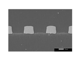
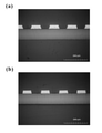
- it is an image which shows a part (an example of a metal wiring) of the flexible circuit board obtained in an Example.
- it is an image which shows a part (an example of a metal wiring) of the flexible circuit board obtained in the comparative example.
- it is an image which shows a part (an example of a metal wiring) of a 4-layer flexible circuit board obtained in an Example.
- the copper-clad laminate 10 of the present embodiment will be described with reference to FIG. ⁇ Copper-clad laminate>
- the copper-clad laminate 10 according to the present embodiment includes at least a resin film 1 as a base material and an electroless copper plating layer 2 laminated on at least one surface of the resin film 1.
- the electrolytic copper plating layer 3 may be formed on the electroless copper plating layer 2.
- the resin film 1 it is preferable to use a so-called low-dielectric resin film having excellent electrical characteristics in the high frequency range as the resin film 1 as the base material.
- the low dielectric resin film films such as known liquid crystal polymers, fluororesins, polyimide resins, modified polyimide resins, epoxy resins, polytetrafluoroethylene resins, and polyphenylene ether resins having lower dielectric losses are preferably used. Be done. These resins may be monopolymers or copolymers. Further, the resin may be used alone or may be used as a hybrid by blending a plurality of resins.
- the electrical characteristics of the resin film 1 as the base material it is preferable that the relative permittivity at a frequency of 10 GHz is 3.5 or less and the dielectric loss tangent is 0.008 or less.
- the thickness of the resin film 1 is not particularly limited, but is preferably 5 ⁇ m to 100 ⁇ m in practical use.
- the electroless copper plating layer 2 in the present embodiment is preferably formed by electroless copper plating. That is, since the resin film 1 has an insulating property, a copper plating layer is formed by electroless plating.
- the electroless copper plating layer 2 may be a seed layer when a flexible circuit board is manufactured by a semi-additive method (SAP method or MSAP method), a subtractive method, a full additive method, or the like.
- the electroless copper plating layer 2 is formed of a Cu—Ni alloy
- the Ni content is 0.01 to 1.2 wt%, and further 0.01 to 1.0 wt%. It is preferably 0.01 to 0.3 wt%, and more preferably 0.01 to 0.3 wt%.
- the electroless copper plating layer 2 is a Cu—Ni alloy, it is considered that blistering is suppressed because the internal stress in the plating layer is also suppressed by containing Ni having a higher plating precipitation property than Cu. Therefore, it is preferable.
- the volume resistivity of the electroless copper plating layer 2 is preferably 6.0 ⁇ ⁇ cm or less, and more preferably 4.5 ⁇ ⁇ cm or less.
- a known method such as a fluorescent X-ray apparatus (XRF) or a plasma emission spectroscopic analyzer (ICP) can be used.
- the electroless copper plating method for forming the electroless copper plating layer 2 a known method may be used as long as the electroless copper plating layer 2 having a predetermined thickness can be formed.
- the method of electroless copper plating will be described in detail with reference to the items of the manufacturing method described later.
- the thickness of the electroless copper plating layer 2 is preferably in the range of 0.1 ⁇ m to 1.0 ⁇ m from the viewpoint of manufacturing efficiency and cost.
- the thickness of the electroless copper plating layer 2 is less than 0.1 ⁇ m, it may not function as a seed layer when the flexible circuit board is manufactured by the semi-additive method, which is not preferable. On the other hand, when the thickness of the electroless copper plating layer 2 exceeds 1.0 ⁇ m, it may be difficult to form a fine circuit pattern when manufacturing a flexible circuit board, which is not preferable.
- the thickness of the electroless copper plating layer 2 is more preferably 0.1 ⁇ m to 0.8 ⁇ m.
- the average surface roughness Ra of the above-mentioned resin film 1 at the interface on the plating layer side in contact with the electroless copper plating layer 2 is 1 to 150 nm, preferably 20 to 150 nm. It is characterized by being.
- the average surface roughness Ra at the interface on the plating layer side in contact with the electroless copper plating layer 2 is preferably 20 to 150 nm.
- the average surface roughness Ra at the interface on the plating layer side in contact with the electroless copper plating layer 2 is preferably 1 to 150 nm, more preferably. 1 to 50 nm is desirable. The reason for this is as follows.
- the transmission characteristics at high frequencies of the GHz band and above are high so that the copper-clad laminate can be suitably applied to a circuit board compatible with high frequencies as described above.
- the transmission signal propagates on the conductor surface at higher frequencies due to the skin effect, and the transmission loss increases as the roughness of the conductor surface increases. Therefore, in the present embodiment, in order to reduce the influence of transmission loss due to the skin effect, it is possible to reduce the average surface roughness Ra of the electroless copper plating layer 2 forming the wiring conductor at the interface with the resin film 1. preferable.
- the average surface roughness Ra of the above-mentioned resin film 1 at the interface on the plating layer side in contact with the electroless copper plating layer 2 is 1 nm to 150 nm. Is.
- the purpose is to achieve both roughness reduction (further reduction of transmission loss) and adhesion between the electroless copper plating layer 2 and the resin film 1.
- the specific adhesion strength between the electroless copper plating layer 2 and the resin film 1 is preferably 4.2 N / cm or more in practical use. Further, the above-mentioned adhesion strength is more preferably 5.0 N / cm or more, further preferably 6.4 N / cm or more.
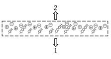
- FIG. 2 schematically shows the state of the interface between the resin film 1 and the electroless copper plating layer in the copper-clad laminate 10 of the present embodiment. That is, it is preferable that a hydroxyl group and / or a carboxyl group is imparted to the interface of the resin film 1 on the electroless copper plating layer 2 side. This is due to the following reasons.
- the electroless copper plating layer 2 when the electroless copper plating layer 2 is formed on at least one surface of the resin film 1 by electroless plating, it is plated on the surface of the resin film 1.
- the metal palladium which is the core of formation, is applied.
- this metallic palladium those produced by a palladium catalyst can be applied.
- hydroxyl groups and / or carboxyl groups at the interface between the resin film 1 and the electroless copper plating layer 2 can be confirmed by a known surface analysis method.
- known analysis methods such as Fourier transform infrared spectrophotometer (FT-IR), X-ray photoelectron spectroscopy (ESCA), and time-of-flight secondary ion mass spectrometry (TOF-SIMS) can be used. be.
- the peak at the mass 121 is obtained as a result of analysis by the flight time mass spectrometry (TOF-SIMS) on the side of the electroless copper plating layer 2.
- the strength is preferably 800 (0.12 amu bin) or more. That is, in the present embodiment, as a result of analysis by TOF-SIMS, it is preferable that a functional group having a mass of 121 and containing a hydroxyl group and / or a carboxyl group is present at the interface between the resin film 1 and the electrolytic copper plating layer 2.
- the functional group having a mass of 121 is preferably any of the following structural formula 1 or structural formula 2, but structural formula 1 is particularly preferable.
- the "functional group containing a hydroxyl group and / or a carboxyl group” imparted to the interface between the resin film 1 and the electroless copper plating layer 2 is not limited to the above. Further, as long as the "functional group containing a hydroxyl group” is added, the “functional group containing a carboxyl group” may not be added. And vice versa. Further, both a “functional group containing a hydroxyl group” and a “functional group containing a carboxyl group” may be imparted.
- the interface between the resin film 1 and the electrolytic copper plating layer 2 is provided with more "functional groups containing hydroxyl groups” than "functional groups containing carboxyl groups".
- the "functional group containing a hydroxyl group” is added and the "functional group containing a carboxyl group” is not added.
- the electrolytic copper-plated layer 3 is further formed on the electrolytic-free copper-plated layer 2 described above as the copper-clad laminate 20. May be good. That is, when the flexible circuit board is manufactured by the semi-additive method, it is also possible to use the electroless copper plating layer 2 as a seed layer to form a resist pattern and then further form the electrolytic copper plating layer 3.
- the method for forming the flexible circuit board using the copper-clad laminate of the present embodiment is not limited to the semi-additive method described above, and other known methods such as the full additive method and the subtractive method can be applied. be.
- the electroless copper plating layers are formed on both sides of the resin film and the through holes H are formed as shown in FIG. That is, it is preferable that the resin film 1 has a through hole in its cross section, and the through hole H is formed so that at least a part of the electroless copper plating layer 2 covers the inner surface of the through hole. It is preferable to form such a through hole H when the copper-clad laminate of the present embodiment is used for a flexible circuit board application. Since the position and size of the through hole H can be appropriately determined by the flexible circuit board to be manufactured, detailed description thereof will be omitted.
- the copper-clad laminate in the present embodiment includes the resin film 1 and the electrolytic copper plating layer 2 as described above, but for example, when it takes time to form the electrolytic copper plating layer 3 described above. Further, even if a known protective layer (not shown) for preventing oxidation of the electrolytic copper plating layer 2 is formed on the surface of the electrolytic copper plating layer 2 (the side opposite to the resin film 1). good.
- the protective layer of the electroless copper plating layer 2 is intended for suppressing oxidation, for example, and is formed by performing a rust preventive treatment by a known method.
- resist patterning resist formation (coating or bonding) / exposure / patterning
- electrolytic copper plating removal of patterned resist
- electrolytic copper plating layer electrolytic copper plating layer.
- the desired circuit pattern is formed by etching.
- L / S (line & space) constituting the circuit pattern is narrowed in pitch for the purpose of improving performance, and how precisely this circuit pattern is formed is important.
- the electrolytic copper plating layer 2 as the seed plating layer is formed, the electrolytic copper plating layer is formed on the electrolytic copper plating layer 2 after defining the circuit pattern by a resist. Has been done. At this time, if the electrolytic copper plating layer is heated (annealed) for the purpose of releasing the internal stress of the electrolytic copper plating layer, the resist is cured by this heat treatment, and the resist can be removed later. It will be difficult.
- the size of the crystallites in the electroless copper plating layer 2 is controlled by performing the above-mentioned heating (baking) treatment before the above-mentioned resist patterning, and the entire conductive coating film ( It is possible to further improve the volume resistance of the electrolytic copper plating layer 2 while ensuring good adhesion between the electrolytic copper plating layer 2 and the electrolytic copper plating layer 3) and the low dielectric resin film.
- the electrolytic copper plating layer 3 shown in FIG. 4 or the like is further formed on the electroless copper plating layer 2 described above.
- the electrolytic copper plating layer 3 is preferably formed by electrolytic plating.
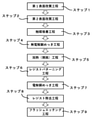
- a method for manufacturing the copper-clad laminate 10 of the present embodiment will be described with reference to FIG.
- a method for producing the copper-clad laminate 10 in the present embodiment a first surface modification step (step 1) of imparting a carboxyl group and / or a hydroxyl group on at least one surface of the resin film 1 and the above-mentioned carboxyl group and / Or a second surface modification step (step 2) in which a charge is applied to the surface to which a hydroxyl group is applied by a wet method, and a catalyst adsorption step (step 3) in which a catalyst is adsorbed on the surface to which the charge is applied.
- the electroless copper plating step (step 4) of forming the electroless copper plating layer 2 on the surface on which the catalyst is adsorbed, and the copper-clad laminate on which the electroless copper plating layer is formed.
- the heating (baking) step (step 5) of heating is included.
- the second surface modification step of step 2 is not essential, and may be appropriately omitted depending on the material of the resin film 1 and the molar ratio in the first surface modification step.
- the method for manufacturing the copper-clad laminate 20 in the present embodiment includes a step of forming an electrolytic copper-plated layer, and heats (bends) the copper-clad laminate on which the electrolytic-free copper-plated layer is formed.
- a resist patterning step (step 6) in which a resist is formed (coated or bonded) on the electrolytic copper plating layer after the step (step 5), and an electrolytic copper plating layer 3 is formed between the patterned resists.
- the electrolytic copper plating step (step 7), the resist removing step (step 8) for removing the patterned resist, and the flash etching step (step 9) for etching the electrolytic copper plating layer after removing the resist may be included. ..
- steps 2 and 6 to 9 may be omitted as appropriate.
- steps 6 and 6 to 9 may be omitted, or steps 2 and 6 to 9 may be omitted.
- the resin film 1 constituting the copper-clad laminate is LCP, it is desirable to have the above-mentioned second surface modification step, but when the resin film 1 is MPI (modified polyimide) or PI, it is desirable. May omit the second surface modification step.
- the method for producing the copper-clad laminate 10 in the present invention includes a electroless copper plating step of forming the electroless copper plating layer 2 on at least one surface of the resin film 1, and the electroless copper. It includes at least a heating (baking) step of heating the copper-clad laminate on which the plating layer is formed before the resist patterning step.
- a heating (baking) step of heating the copper-clad laminate on which the plating layer is formed before the resist patterning step.
- the resin film 1 used is preferably a so-called low-dielectric resin film.
- the relative permittivity at a frequency of 10 GHz is 3.5 or less and the dielectric loss tangent is 0.008 or less.
- a carboxyl group and / or a hydroxyl group is imparted to at least one surface of the resin film 1.
- the method for imparting the carboxyl group and / or the hydroxyl group include a method in which a mixed solution of an alkaline aqueous solution and an amino alcohol is brought into contact with at least one surface of the resin film 1.
- the alkaline aqueous solution used in the first surface modification step may be either an inorganic alkali or an organic alkali.
- the inorganic alkali include alkali metal hydroxides such as sodium hydroxide and potassium hydroxide, or carbonates thereof.
- the organic alkali include tetraalkylammonium hydroxide and the like. The above-mentioned alkalis may be used alone or in combination of two or more.
- the amino alcohol used in the first surface modification step may be specifically an aliphatic amino alcohol or an aromatic amino alcohol. Moreover, it may be a derivative thereof.
- amino alcohol ethanolamine, heptaminol, isoetaline, butanolamine, propanolamine, sphingosine, methanolamine, dimethylethanolamine, N-methylethanolamine and the like can be used. Of these, it is particularly preferable to apply aminoethanol.
- the molar ratio within the above range, both roughness reduction (further reduction of transmission loss) and adhesion between the electroless copper plating layer 2 and the resin film 1 which are the objects of the present invention are achieved. Can be done. The reason is not clear at this time, but as a result of the examination by the inventors, it is presumed that the reason is as follows.
- the mixed solution having a molar ratio of (-NH 2 groups / -OH groups) within the above range is the first.
- the average surface roughness Ra of the surface on the electroless copper plating layer 2 side can be 1 nm to 150 nm as the state of the surface of the resin film 1. Therefore, when the wiring conductor is formed on the circuit board by the electroless copper plating layer, the transmission loss due to the skin effect is suppressed, and it becomes possible to exhibit preferable transmission characteristics.
- the present inventors have come up with the idea of achieving the object of the present invention by going through the first surface modification step as described above.
- a known method can be appropriately applied, for example, the resin film 1 is immersed in the mixed solution.
- examples thereof include a method and a method of spraying the mixed solution onto the resin film 1 by spraying or the like.
- a method other than the above-mentioned method may be applied as long as it is a method capable of imparting a carboxyl group and / or a hydroxyl group to the surface of the resin film 1.
- the precipitation property of the plating and the adhesion of the plating can be improved by adjusting the contact angle of the film surface.
- the contact angle at the interface on the plating layer side in contact with the electroless copper plating layer 2 is preferably 30 ° or less.
- the contact angle at the interface on the plating layer side in contact with the electroless copper plating layer 2 is preferably 45 ° or less.
- the second surface modification step in the present embodiment is preferably a step performed after the first surface modification step described above. In other words, it is not always necessary to perform the second surface modification step after the first surface modification step, and as described above, the second surface modification step as this step 2 can be omitted as appropriate.
- Such a second surface modification step is a step of imparting a carboxyl group and / or a hydroxyl group on the surface of the resin film 1 in the first surface modification step, and then further adding an electric charge. It is preferable because it is possible to improve the adhesion between the resin film 1 and the electroless copper plating layer 2 by applying an electric charge.
- the metallic palladium which is the core of the plating growth, is present on the resin film 1. Then, in order for this metallic palladium to firmly adhere to the resin film 1, it is preferable that the surface of the resin film 1 has at least a negative charge.
- a step of further applying a positive charge to the surface of the resin film 1 and a step of further applying a negative charge to the surface to which the positive charge is applied are performed. It is preferable to include it. By going through these steps, it is possible to reliably attach a negative charge to the surface of the resin film 1, so that from the viewpoint of the above-mentioned adhesion of metallic palladium and the adhesion of the electroless copper plating layer 2. Is preferable.
- the resin film 1 after imparting a carboxyl group and / or a hydroxyl group to the surface is further known as a cationic surfactant. It is possible to apply a method of immersing in an agent, a method of bringing a known cationic surfactant into contact with the resin film 1 by spraying, or the like. Further, in the step of adsorbing a negative charge on the surface of the resin film 1, similarly, a method of immersing in a known anionic surfactant, a method of spraying, or the like can be applied.
- the second surface modification step of the present embodiment is preferably performed by a wet method as described above. By performing it in a wet manner, it is suitable for mass production by reel-to-reel or the like, and has an advantage that cost can be reduced.
- the catalyst adsorption step of the present embodiment is a step of further adsorbing the catalyst on the surface of the resin film 1 with respect to the resin film 1 to which at least a negative charge is applied to the surface by the second surface modification step described above. ..
- a known catalyst solution can be brought into contact with the surface of the resin film 1 by a known method.
- the catalyst Cu, Ni, Pd, Ag and the like can be used.
- the known catalyst solution for example, a tin-palladium-based catalyst solution or a palladium colloid-based catalyst solution can be used, but the catalyst solution is not limited thereto.
- the amount of the catalyst applied to the resin film 1 is preferably 15 ⁇ g / dm 2 or less as metallic palladium.
- the lower limit of the catalyst should be as small as possible in consideration of etching during circuit formation, but it must be applied to the extent that the electroless copper plating layer is well formed, and it may be 1 ⁇ g / dm 2 or more. preferable.
- the amount of metallic palladium applied to the resin film 1 exceeds the above value, the insulation reliability between the circuits when the flexible circuit board is used may decrease, which is not preferable.
- the amount of metallic palladium can be obtained by a known measuring method. For example, it can be obtained by a method such as peeling only copper from the resin film 1, dissolving the palladium residue on the resin film 1 with nitric acid, and measuring the amount of the residue by ICP.
- the electroless copper plating step is preferably performed after the catalyst adsorption step.
- known baths such as an EDTA bath, a Rochelle bath, and a triethanolamine bath can be used.
- the copper-clad laminate 10 according to the present embodiment is manufactured.
- the immersion time of the resin film 1 in the plating bath may be appropriately determined so that the thickness of the electroless copper plating layer 2 is 0.1 to 1.0 ⁇ m.
- the copper-clad copper plating layer 2 is formed after the electroless copper plating layer 2 is formed on the resin film 1 and before the resist patterning. It has a heating (baking) step (step 5) for heating the laminate.
- the heating (annealing) step of this step 5 has the purpose of, for example, coarsening the crystallite size in the copper plating layer to cause structural transformation, and also the purpose of releasing the internal stress of the electroless copper plating layer (aging purpose). It may be done in such a way.
- heating conditions in such a heating (annealing) step are preferably performed under the following heating conditions, for example.
- the above atmosphere may be in the atmosphere, in an inert gas, or in a vacuum, and the types of the inert gas include nitrogen gas, a mixed gas of hydrogen and nitrogen, argon gas, helium gas, and the like. Can be used. From the viewpoint of cost, it is preferably in the atmosphere or in an inert gas. Further, the heating atmosphere is more preferably an inert gas atmosphere or a vacuum in order to suppress the formation of the oxide film.
- Particularly preferable ranges of the heating time and temperature when the heating (annealing) treatment is performed in the atmosphere are a heating temperature of 180 to 200 ° C. and a heating (soaking) time of 10 to 60 minutes in order to suppress the formation of an oxide film. Is preferable.
- the heating temperature is 220 to 350 ° C. and the heating (soaking) time is 10 to 180 minutes.
- the elongation characteristics of the electroless copper plating layer 2 are also improved, so that high peel strength can be maintained. Further, by performing the heating (baking) step, it is possible to prevent the electroless copper plating layer 2 from peeling from the resin film 1, and the adhesion between the electroless copper plating layer 2 and the resin film 1 is ensured. can do.
- the resist is patterned (formed (coated or bonded) and patterned according to a desired circuit) by a known method (step 6), and the electrolytic copper plating described above is performed.
- the electrolytic copper plating layer 3 is formed between the resists on the electrolytic copper plating layer 2 (step 7).
- the thickness of the electrolytic copper plating layer 3 is preferably, for example, 10 to 30 ⁇ m. At this time, it is preferable to satisfy at least one that the volume resistivity of the electrolytic copper plating layer 3 is 5.0 ⁇ ⁇ cm or less.
- the electrolytic copper plating step for forming the electrolytic copper plating layer 3 a known copper sulfate bath, copper pyrophosphate bath, or the like can be applied. Further, the electrolytic plating conditions (pH, temperature, current density, immersion time, etc.) can be appropriately selected based on the thickness of the electrolytic plating layer and the like. Through the above steps, the copper-clad laminate 20 according to the present embodiment is manufactured.
- the flexible circuit board in the present embodiment is preferably a flexible circuit board in which a circuit is formed by the electroless copper plating layer 2 of the copper-clad laminate 10 described above.
- the surface roughness Ra between the resin film 1 and the electroless copper plating layer 2 is equal to or less than a predetermined value, so that the transmission loss as a flexible circuit board can be reduced. It is possible to suppress it.
- the electrolytic copper plating layer A known resist patterning step of forming (coating or bonding) and patterning a resist is performed on the resist 2, and then the electrolytic copper plating step described above is performed to form an electrolytic copper plating layer 3 between the patterned resists. Will be done.
- FIG. 7A schematically shows the flexible circuit board 100 made of the copper-clad laminate 20 (that is, the copper-clad laminate in which the electrolytic copper plating layer 3 is further formed on the electroless copper plating layer 2) in the present embodiment. show.
- the metal wiring MW having a specific conductor shape obtained by the present embodiment forms at least a part of the circuit.
- the copper-clad laminate 20 is used for at least a part of the conductor (metal wiring) forming the circuit, and the metal wiring by the conventional method is used for the other circuit parts. It may be formed.
- the wiring height from the resin film 1 is Hw
- the width of the base in contact with the resin film 1 is Lb
- the width of the upper surface of the metal wiring MW is Lt.
- the distance between the wirings with other adjacent metal wirings MW on the resin film 1 is S, it is preferable to satisfy the following formula (1).
- a in the formula (1) indicates the rectangularness of the conductor shape in the cross section of the metal wiring MW in the width direction orthogonal to the direction in which the current flows.
- the metal wiring MW in the flexible circuit board 100 preferably satisfies the following formula (2) in addition to the above formula (1). Distance between wirings S ⁇ 60 ⁇ m ⁇ ⁇ ⁇ (2)
- the metal wiring MW in the flexible circuit board 100 has the following equation (3) when the value (S / A) obtained by dividing the distance S between wirings by the rectangularity A of the conductor shape described above is defined as the conductor wiring density WD. It is preferable to satisfy. Conductor wiring density WD ⁇ 10.0 ... (3)
- the rectangularity A of the conductor shape described above should be as close to a rectangle as possible, and the distance S between wirings described above should be made as small as possible. Is required.
- the value of the rectangularity A of the conductor shape is set to 2.5 or more, the above-mentioned inter-wiring distance S is set to 60 ⁇ m or less, and the conductor wiring density WD is 10. It was concluded that it was preferable to set it to 0 or less.
- the rectangularity A of the conductor shape is rectangular (A ⁇ 2.5), and the cross section (conductor shape) in the width direction in the metal wiring MW is substantially rectangular. Therefore, while reducing the wiring resistance, the acute-angled portion on the bottom side is relatively obtuse compared to the non-rectangular shape (for example, a trapezoidal shape with a relatively large base), so that the decrease in transmission loss such as high-frequency current is suppressed. It becomes possible to do.
- FIG. 7B schematically shows a flexible circuit board 200 on which a conductor layer is laminated using the copper-clad laminate 20 in the present embodiment. That is, in the flexible circuit board 200 of the present embodiment, a pair of conductor layers CL1 are formed on the outermost layers, and a conductor layer CL2 in which the metal wiring MW of the present embodiment is formed between the pair of conductor layers CL1. It is configured to include a known dielectric layer such as an adhesive layer BL for adhering a conductor layer. In this case, the above-mentioned conductor layer CL1 and conductor layer CL2 both indicate an electric conductor layer arranged on the same plane, and a vertical conductive layer formed such as a via hole or a through hole in the copper-clad laminate 20. Is not targeted.
- a known dielectric layer such as an adhesive layer BL for adhering a conductor layer.
- the above-mentioned conductor layer CL1 and conductor layer CL2 both indicate an electric conductor layer arranged on the same plane, and
- the number of layers of the conductor layer CL is defined as the number of layers.
- the flexible circuit board 200 is laminated with at least four or more conductor layers CL including the metal wiring MW described above.
- the flexible circuit board 200 has an average thickness of 50 ⁇ m or less obtained by dividing the total thickness TA (distance between the outermost conductor layers) of the conductor layer CL by the number of layers of the conductor layer CL (4 layers in FIG. 7B). Is preferable.
- the wiring in the flexible circuit board can be made finer and thinner, and the thickness of the dielectric layer in the multilayer wiring board can be reduced to achieve high density. It is possible to improve the fine wiring performance at the same time.
- the copper-clad laminate 10 is first formed by going through the steps up to step 5 described above.
- the copper-clad laminate 10 on which the above-mentioned electroless copper plating layer 2 (for example, electroless Cu—Ni layer) is formed is provided.
- the above-mentioned through-hole H having a diameter of about 70 to 100 ⁇ m may be appropriately formed, and the position and size of the through-hole H may be determined by the flexible substrate. It can be determined as appropriate according to the specifications. Further, for the formation of the through hole H, two types of drilling and laser machining can be exemplified.
- a through hole may be drilled at a predetermined position by high-speed rotation using a known mechanical drill.
- two types of known CO 2 laser and UV-YAG laser can be exemplified.
- laser processing is suitable, and it is particularly preferable to use a UV-YAG laser.
- a known desmear treatment may be performed after the through holes H are formed by the above method.
- a resist is formed (bonded or coated) on the electroless copper plating layer 2 of the copper-clad laminate 10 described above by a known method to perform patterning (step 6 above).
- a DFR dry film resist
- a resist pattern may be formed on the electroless copper plating layer 2 by performing a treatment and a development treatment.
- DFRs examples include Sunfort (registered trademark) manufactured by Asahi Kasei E-Materials, Fotec (registered trademark) manufactured by Showa Denko Materials, and Riston (registered trademark) manufactured by DuPont. Can be applied. Further, after the above-mentioned resist pattern is formed, it is preferable to perform, for example, a known plasma ashing treatment (as an example, plasma treatment in a mixed gas atmosphere of CF 4 and O 2 ) in order to remove the resist residue.
- a known plasma ashing treatment as an example, plasma treatment in a mixed gas atmosphere of CF 4 and O 2
- electrolytic copper plating bath (as an example, a plating bath shown by the following bath composition) is used.
- the electrolytic copper plating layer 3 is formed on the plating layer 2 (step 7 above).
- the thickness of the electrolytic copper plating layer 3 is preferably, for example, 10 to 30 ⁇ m. No further heat treatment was performed on the electrolytic copper plating layer 3.
- Bath composition Copper sulfate hexahydrate 200 g / L Sulfuric acid 50g / L Chloride ion 50ppm Brightener 5 ml / L (Okuno Pharmaceutical's additive Top Lucina (registered trademark)) Bath temperature: 20-25 ° C Current density: 2.0-3.0A / dm 2
- the resist is removed by a known method (step 8 above). That is, since the above DFR is used as the resist material in this example, for example, any of known NaOH aqueous solution, amine-based stripping solution, and inorganic stripping solution can be used for peeling the DFR.
- a known flash etching for finishing each wiring pattern is performed (step 9 above).
- a sulfuric acid / hydrogen peroxide solution can be used as a soft etching agent, for example, "Evachem (registered trademark) Fine Etch FE-830 (II)” and “Evachem (registered)” manufactured by JCU Co., Ltd.
- a known treatment solution such as "Fine Etch SAC” can be applied.
- the flexible circuit board 100 in which the desired metal wiring is patterned can be manufactured.
- a known adhesive layer BL for multi-layer FPC for example, AU manufactured by Arisawa Seisakusho, SAFY manufactured by Nikkan Kogyo, Vecstar (registered trademark) CTF manufactured by Kuraray, R-BM17 manufactured by Panasonic, etc.
- the flexible circuit board 200 (multilayer flexible circuit board) of the present embodiment described above can be manufactured by laminating a plurality of arbitrary flexible circuit boards 100 using a known bonding sheet (of ⁇ 25 ⁇ m).
- a method of laminating the flexible circuit board 100 As a method of laminating the flexible circuit board 100, a method of vacuum batch pressing while heating to a temperature at which the film layer softens in a state where a predetermined number of flexible substrates are stacked, or a method of vacuum batch pressing the above bonding sheet is performed on the flexible circuit board 100. Examples thereof include a method of attaching to one side or both sides and adhering with a hot press.
- Example 1 a liquid crystal polymer film (Vecstar CTQLCP, manufactured by Kuraray Co., Ltd., thickness: 50 ⁇ m) was prepared as the resin film 1.
- the electrical characteristics the relative permittivity at 10 GHz was 3.3, and the dielectric loss tangent at 10 GHz was 0.002.
- both sides of the prepared resin film 1 are immersed in a mixed solution of potassium hydroxide aqueous solution and monoethanolamine for 5 minutes as a first surface modification step, and carboxyl groups and / or hydroxyl groups are added to both surfaces. It was introduced and washed with immersion water.
- the temperature of the mixed solution used was 40 ° C., and the molar ratio of -OH group and -NH 2 group (-NH 2 group / -OH group) was 2.29.
- the peak intensity of the mass 121 of TOF-SIMS was 1000.
- both sides of the resin film 1 were immersed in an aqueous solution of a cationic surfactant of 10 g / L for 2 minutes to adsorb positive charges. After soaking and washing with water, it was immersed in an aqueous solution of an anionic surfactant 3 g / L for 1 minute. In this way, after adsorbing the positive charge, the negative charge was adsorbed. Further, as a catalyst adsorption step and an electrolytic copper plating step, the plating catalyst was immersed in an aqueous solution of palladium chloride (PdCl 2 ) (2 g / l, pH 12, 40 ° C.) for 5 minutes and then washed with immersion water.
- PdCl 2 palladium chloride
- an electroless Cu—Ni plating layer of 0.2 ⁇ m was formed by an electroless plating bath.
- the electroless plating conditions are as follows.
- Bath composition Copper sulfate 7.5 g / L Nickel sulfate 0.0065 g / L Rochelle salt 20g / L Sodium hydroxide 5g / L pH: 9 Bath temperature: 32 ° C
- Heating (annealing) treatment In this example, after the electroless copper plating layer 2 was formed, it was heated (annealed) using a dry oven (DY300 manufactured by Yamato Kagaku Co., Ltd.) under the following conditions. ⁇ Heating conditions> Heating temperature: 150 ° C Heating (soaking) time: 60 minutes Heating atmosphere: In the atmosphere
- the Ni content in the obtained electroless Cu-Ni plating layer was determined by a method using a plasma emission spectrophotometer (ICP) described later and found to be 0.09 wt%.
- the electrolytic copper plating conditions were as follows. Bath composition: Copper sulfate hexahydrate 200 g / L Sulfuric acid 50g / L Chloride ion 50ppm Brightener 5 ml / L (Okuno Pharmaceutical's additive Top Lucina (registered trademark)) Bath temperature: 20-25 ° C Current density: 2 to 3 A / dm 2 (2.5 A / dm 2 in this example) pH: less than 1
- the thickness of the obtained electrolytic copper plating layer was 18 ⁇ m.
- This measurement sample was measured with an X-ray photoelectron spectrophotometer (JPS-9200, manufactured by JEOL Ltd., X-ray source: Mg, analysis area: ⁇ 3 mm) to obtain a C1s spectrum. Then, the intensity of the peak derived from the carboxyl group (COO (H) bond) appearing in the binding energy 288.8 eV and the intensity of the peak derived from the CC bond appearing in the binding energy 284.7 eV were calculated. According to the measurement result by the above ESCA, the existence of the carboxyl group could not be confirmed. Next, the surface condition of the measurement sample was confirmed by TOF-SIMS.
- the surface of the measurement sample was analyzed by TOF-SIMS TRIFT-II (manufactured by ULVACFY Co., Ltd.). An untreated resin film sample was used as a control.
- the measurement conditions are as follows. Primary ion: 69 Ga Acceleration voltage: 15kV Measurement range: 100 ⁇ m ⁇ 100 ⁇ m Mass range: 0.5-300 (m / z)
- the obtained copper-clad laminate 10 (thickness of electrolytic copper plating layer: thickness shown in Table 1, thickness of electrolytic copper plating layer: 18 ⁇ m) was subjected to the electroless copper plating layer 2 and the electrolytic copper plating layer 2 using the FeCl 3 solution.
- the electrolytic copper plating layer 3 was peeled off to expose the resin film.
- the surface roughness (Ra) of the exposed resin film was measured with an AFM mode of a laser microscope (Olympus OLS3500) and a viewing angle of 5 ⁇ m ⁇ 5 ⁇ m. The obtained values are shown in Table 2.
- the electroless copper plating layer 2 was peeled off using a FeCl 3 solution in the same manner as described above to expose the resin film.
- the exposed resin film surface was cut out to a size of 20 mm ⁇ 20 mm and used as a measurement sample. 2.0 ⁇ L of pure water was dropped on the surface of this sample, and the contact angle was measured with a contact angle measuring device (DropMaster manufactured by Kyowa Interface Science Co., Ltd.).
- the contact angle of the untreated resin surface used in Example 1 was 65 °.
- Adhesive tape manufactured by Nichiban
- thickness of the electrolytic copper plating layer thickness shown in Table 1
- a tape peeling test was carried out by peeling off the copper plating layer 2 after the copper plating layer 2 was affixed, and when the peeling of the electroless copper plating layer 2 was not visually confirmed, the evaluation result was 0.
- the results are shown in Table 2.
- a sample piece having a size of 40 mm ⁇ 40 mm was cut out from the copper-clad laminate 20 on which the electrolytic copper plating layer 3 was formed, and the cut piece was attached to an aluminum plate with a polyimide tape.
- the 90 ° peel strength was measured as the adhesive strength between the resin film and the electroless copper plating layer as follows. That is, a strip-shaped cut is made in the copper-plated surface at intervals of 5 mm on the surface on which the electrolytic copper plating layer is formed on each test material, and then the strip-shaped end is forcibly peeled off to create a trigger for peeling. , The peeled resin film and the copper-plated part were made.
- volume resistivity ( ⁇ ⁇ cm) of the obtained copper-clad laminate 10 was measured by a four-probe method using Lorester GP (MCP-T600 manufactured by Mitsubishi Chemical Corporation). Table 2 shows the measurement results of this volume resistivity.
- Example 2 The procedure was the same as in Example 1 except that the amount of nickel sulfate (NiSO 4 ) added was 0.013 g / L in the bath composition in electroless plating. The content of Ni in the obtained electroless Cu—Ni plating layer was 0.14 wt%. The volume resistivity of this electroless copper plating layer was 3.82 ⁇ ⁇ cm. The results are shown in Tables 1 and 2.
- Example 3 The procedure was the same as in Example 1 except that the amount of nickel sulfate (NiSO 4 ) added was 0.065 g / L in the bath composition in electroless plating. The content of Ni in the obtained electroless Cu—Ni plating layer was 0.18 wt%. The volume resistivity of this electroless copper plating layer was 3.85 ⁇ ⁇ cm. The results are shown in Tables 1 and 2.
- Example 4 The procedure was the same as in Example 1 except that the amount of nickel sulfate (NiSO 4 ) added was 0.13 g / L in the bath composition in electroless plating. The content of Ni in the obtained electroless Cu—Ni plating layer was 0.41 wt%. The volume resistivity of this electroless copper plating layer was 5.66 ⁇ ⁇ cm. The results are shown in Tables 1 and 2.
- Example 5 The procedure was the same as in Example 1 except that the amount of nickel sulfate (NiSO 4 ) added was 0.325 g / L in the bath composition in electroless plating. The content of Ni in the obtained electroless Cu—Ni plating layer was 0.74 wt%. The volume resistivity of this electroless copper plating layer was 5.98 ⁇ ⁇ cm. The results are shown in Tables 1 and 2.
- Example 7 The procedure was the same as in Example 6 except that the amount of nickel sulfate (NiSO 4 ) added was 0.013 g / L in the bath composition in electroless plating. The content of Ni in the obtained electroless Cu—Ni plating layer was 0.14 wt%. The volume resistivity of this electroless copper plating layer was 2.28 ⁇ ⁇ cm. The results are shown in Tables 1 and 2.
- Example 8> The procedure was the same as in Example 6 except that the amount of nickel sulfate (NiSO 4 ) added was 0.065 g / L in the bath composition in electroless plating. The content of Ni in the obtained electroless Cu—Ni plating layer was 0.18 wt%. The volume resistivity of this electroless copper plating layer was 2.26 ⁇ ⁇ cm. The results are shown in Tables 1 and 2.
- Example 9 The procedure was the same as in Example 6 except that the amount of nickel sulfate (NiSO 4 ) added was 0.13 g / L in the bath composition in electroless plating. The content of Ni in the obtained electroless Cu—Ni plating layer was 0.41 wt%. The volume resistivity of this electroless copper plating layer was 4.47 ⁇ ⁇ cm. The results are shown in Tables 1 and 2.
- Example 10 The procedure was the same as in Example 6 except that the amount of nickel sulfate (NiSO 4 ) added was 0.325 g / L in the bath composition in electroless plating. The content of Ni in the obtained electroless Cu—Ni plating layer was 0.74 wt%. The volume resistivity of this electroless copper plating layer was 4.97 ⁇ ⁇ cm. The results are shown in Tables 1 and 2.
- Example 11 The procedure was the same as in Example 6 except that the amount of nickel sulfate (NiSO 4 ) added to the bath composition in electroless plating was 0.65 g / L and the plating thickness of electroless plating was 0.3 ⁇ m. .. The content of Ni in the obtained electroless Cu—Ni plating layer was 1.18 wt%. The volume resistivity of this electroless copper plating layer was 5.54 ⁇ ⁇ cm. The results are shown in Tables 1 and 2.
- the resin film 1 was made of modified polyimide (MPI), and as the first surface modification step, a surface modification mixture was obtained by further mixing 40% by volume of a mixture of an aqueous potassium hydroxide solution and monoethanolamine with 60% by volume of water.
- the second surface modification step was omitted, the plating thickness of the electroless Cu-Ni plating layer 2 was 0.3 ⁇ m, and the heating temperature in the heating (baking) step was set to 220 ° C.
- the same procedure as in Example 8 was carried out except that the heat) time was set to 30 minutes.
- Example 13 The same procedure as in Example 12 was carried out except that the heating temperature in the heating (annealing) step was set to 300 ° C. and the heating (soaking) time was set to 60 minutes. The results are shown in Tables 1 and 2.
- Example 14 As the FCCL (flexible copper-clad laminate), the copper-clad laminate 20 manufactured in Example 6 above was used. A known DFR (dry film resist) was attached to the copper-clad laminate 20 by a known roll laminator. Next, the negative portion in the resist was cured by UV exposure with a known exposure apparatus through a mask on which a predetermined resist pattern image was formed.
- FCCL flexible copper-clad laminate
- DFR dry film resist
- an unexposed portion in the resist was eluted with a known alkaline developer such as 1 mass% sodium carbonate aqueous solution as a developer to form a resist pattern on the electrolytic copper plating layer.
- a known alkaline developer such as 1 mass% sodium carbonate aqueous solution as a developer
- plasma treatment was performed in a known mixed gas atmosphere of CF 4 and O 2 to remove the resist residue.
- the FCCL of this example on which the resist pattern obtained above was formed was pickled by immersing it in a 5% by weight solution of sulfuric acid at 30 ° C. for 30 seconds before electrolytic plating, and electroless copper was used. The oxide film on the plating layer was removed.
- electrolytic copper plating was formed on the electroless copper plating layer on which the resist pattern was formed so as to have a predetermined wiring height Hw shown in Table 3.
- Bath composition Copper sulfate hexahydrate 70 g / L 98% sulfuric acid 200g / L 35% hydrochloric acid 0.15 ml / L Additives Okuno Pharmaceutical's Top Lucina (registered trademark) SF base WR 2.5 ml / L, Top Lucina (registered trademark) SF-B 1.0 ml / L, and Top Lucina® SF Leveler 5.0ml / L Bath temperature: 25 ° C Current density (cathode): 3.0 A / dm 2
- the resist pattern was removed by spraying the above resist pattern with a known amine-based stripping solution for 180 seconds with respect to the FCCL of this example in which electrolytic copper plating was formed. Further, as the above-mentioned flash etching treatment, an etching bath having the following composition was prepared and spray-treated at 25 ° C. for 30 seconds.
- the flexible circuit board (FPC) of this embodiment was obtained.
- a cross section is cut in the width direction (direction orthogonal to the current direction) in the predetermined metal wiring, and the above-mentioned wiring is performed by a known electron microscope by the following method.
- the height Hw, the width Lb at the bottom, the width Lt at the top surface, the rectangularity A of the conductor shape, the distance S between wirings, and the conductor wiring density WD were measured. That is, first, tangent lines are drawn on the bottom surface, the top surface, and both side surfaces of the metal wiring with respect to the cross-sectional photograph obtained by the above-mentioned electron microscope.
- Example 15 The same procedure as in Example 14 was carried out except that the photomask for exposure was changed to the photomask for exposure designed to have the base width Lb and the distance S between the wirings shown in Table 3. The obtained results are shown in Table 3. Further, a part of the obtained flexible circuit board (an example of metal wiring) is shown in FIG.
- Example 16> The copper-clad laminate 20 manufactured in Example 8 above was used as the FCCL (flexible copper-clad laminate), and the base width Lb and the distance between wirings S shown in Table 3 were designed for exposure. The procedure was the same as in Example 15 except that the photomask was changed. The obtained results are shown in Table 3.
- the metal wiring MW of the flexible circuit board obtained in Example 17 the difference (Lb-Lt) between the width Lb at the bottom and the width Lt at the top surface was almost 0 (zero). Therefore, the rectangularity A of the conductor shape in this embodiment is regarded as “ ⁇ ” because it is almost infinite ( ⁇ ), and the conductor wiring density WD is also regarded as “0” because it is almost zero (0). Rectangle.
- Example 17 The same procedure as in Example 16 was carried out except that the photomask for exposure was changed to the photomask for exposure designed to have the base width Lb and the distance S between the wirings shown in Table 3. The obtained results are shown in Table 3.
- Example 18 The same procedure as in Example 16 was carried out except that the photomask for exposure was changed to the photomask for exposure designed to have the base width Lb and the distance S between the wirings shown in Table 3. The obtained results are shown in Table 3.
- Example 19 After adjusting the electroless plating bath, polyethylene glycol having a weight average molecular weight of 1,000 was added to the electroless plating bath to a concentration of 0.8 g / l, the heating temperature was set to 250 ° C., and the heating (soaking) time. The same procedure as in Example 8 was carried out except that the setting was 30 minutes and the plating thickness of the electroless plating was set to 0.3 ⁇ m. The results are shown in Tables 1 and 2.
- Example 20 After adjusting the electroless plating bath, the same procedure as in Example 19 was carried out except that polyethylene glycol having a weight average molecular weight of 1,000 was added to the electroless plating bath to a concentration of 1.0 g / l. The results are shown in Tables 1 and 2.
- Example 21 As the first surface modification step, a mixed solution for first surface modification was prepared by mixing 80% by volume of water with 20% by volume of the mixed solution of potassium hydroxide aqueous solution and monoethanolamine, and the second surface. The reforming was performed, the plating thickness of the electroless Cu-Ni plating layer 2 was 0.1 ⁇ m, the heating temperature in the heating (baking) step was 250 ° C, and the heating (soaking) time was 30 minutes. Except for what was done, the same procedure as in Example 12 was performed. The results are shown in Tables 1 and 2.
- Example 22 As the first surface modification step, a mixed solution for first surface modification was prepared by mixing 85% by volume of water with 15% by volume of the mixed solution of potassium hydroxide aqueous solution and monoethanolamine, and the second surface. The modification was carried out, the plating thickness of the electroless Cu-Ni plating layer 2 was 0.1 ⁇ m, the heating temperature in the heating (baking) step was 250 ° C, and the heating (soaking) time was 30 minutes. Except for what was done, the same procedure as in Example 12 was performed. The results are shown in Tables 1 and 2.
- Example 23 The copper-clad laminate 20 manufactured in Example 21 described above was used as the FCCL (flexible copper-clad laminate), and the base width Lb and the distance between wirings S shown in Table 3 were designed for exposure. The procedure was the same as in Example 14 except that the photomask was changed. The obtained results are shown in Table 3.
- Example 24 A metal wiring pattern is formed on both sides in the same manner as in Example 14, except that the wiring height Hw is 12 ⁇ m and the L / S (Line & Space, which corresponds to Lb / S in this embodiment) is 20 ⁇ m / 20 ⁇ m.
- the flexible circuit board (FPC) was manufactured. This substrate is used as the core layer.
- a commercially available single-sided copper-clad laminate having a liquid crystal polymer having a thickness of 25 ⁇ m and having a copper foil having a thickness of 12 ⁇ m on one side was prepared.
- a single-sided flexible circuit board having a metal wiring pattern formed by a known subtractive method was produced. This is used for the outer layer.
- a commercially available bonding sheet (thickness 15 ⁇ m) is arranged on both sides of the core layer, and this one-sided flexible circuit board is laminated on both outer layers so that the copper foil is on the outside, and then bonded and laminated by a high temperature press.
- a 4-layer flexible circuit board was obtained.
- the total thickness TA of the obtained four-layer flexible circuit board was 154 ⁇ m, and the thickness per conductor layer layer was 38.5 ⁇ m.
- the four-layer flexible circuit board obtained in this embodiment was a high-density and fine wiring having four conductor layers. Furthermore, we have obtained a multi-layered flexible circuit board that has both high flexibility and transmission characteristics.
- FIG. 10 shows a cross-sectional image (photographed with an electron microscope) of a part of the 4-layer flexible circuit board obtained in this embodiment.
- Example 1 The procedure was the same as in Example 1 except that the conditions for electroless plating were as follows. That is, in Comparative Example 1, electroless Cu plating was performed by setting the addition amount of nickel sulfate (NiSO 4 ) to 0. [Electroless plating conditions] Bath composition: Copper sulfate 7.5 g / L Rochelle salt 20g / L Sodium hydroxide 5g / L pH: 9 Bath temperature: 32 ° C
- FCCL flexible copper-clad laminate
- the thickness of the liquid crystal polymer film of FCCL was 50 ⁇ m
- the thickness of the electrolytic copper foil was 18 ⁇ m.
- the prepared FCCL was subjected to electrolytic copper plating by a known method so that the thickness of the metal wiring (wiring height Hw) was 30 ⁇ m.
- a flexible circuit board (FPC) was manufactured by using the known subtractive method shown below. That is, a known DFR (dry film resist) was attached to the obtained copper-clad laminate by a known roll laminator. Next, the positive portion in the resist was cured by UV exposure with a known exposure apparatus through a mask on which a predetermined resist pattern image was formed. It was
- Comparative Example 5 Similar to Comparative Example 2 except that a liquid crystal polymer film 50 ⁇ m and a rolled copper foil 18 ⁇ m were used as the copper-clad laminate, and the thickness (wiring height Hw) of the metal wiring after electrolytic copper plating was 29.2 ⁇ m. Went to. The results are shown in Table 3. Further, a part of the obtained flexible circuit board (an example of metal wiring) is shown in FIG. 9 (b).
- the copper-clad laminate of the present invention can realize good plating precipitation and good volume resistivity of the electroless copper plating layer. Therefore, it is clear that the copper-clad laminate of the present invention is suitably applied to a wiring board or the like that requires fine wiring having a multi-layer structure.
Landscapes
- Chemical & Material Sciences (AREA)
- Engineering & Computer Science (AREA)
- Materials Engineering (AREA)
- Chemical Kinetics & Catalysis (AREA)
- Metallurgy (AREA)
- Organic Chemistry (AREA)
- Microelectronics & Electronic Packaging (AREA)
- Mechanical Engineering (AREA)
- General Chemical & Material Sciences (AREA)
- Electrochemistry (AREA)
- Manufacturing & Machinery (AREA)
- Inorganic Chemistry (AREA)
- Manufacturing Of Printed Wiring (AREA)
- Laminated Bodies (AREA)
- Chemically Coating (AREA)
Abstract
Description
特に昨今ではIoTによるビッグデータに代表される情報の大容量化に伴い、電子機器間における通信信号の高周波化が進んでおり、かような通信機器に搭載される回路基板には高周波領域における伝送損失(誘電損失)の低い材料が要求される。
かようなフレキシブル回路基板(以下、「FPC」とも称する)は、例えばスパッタ法やめっき法などによって、低誘電フィルム上に銅などの導電性皮膜が形成される。このうちスパッタ法によってFPCを製造する場合には、製造工程が煩雑になる結果、その生産性やコスト面で多くの課題が残ってしまう。
ここで、本発明者らが鋭意検討した結果、この無電解銅めっき層が上記した低誘電フィルム上で良好な析出性を示すには、無電解銅めっき層中におけるNiの存在が重要であることを突き止めた。そして検討を進める過程において、単にNiが無電解銅めっき層中において存在すればよいのではなく、無電解銅めっき層におけるNiの含有率が少ない場合にはめっき析出性が悪化する一方で多過ぎる場合には体積抵抗率が増加して磁性を帯びてしまうことに帰結した。
また、上記した(12)におけるフレキシブル回路基板においては、前記金属配線を含む導体層を有して少なくとも4層以上積層されてなり、全体の厚みを前記導体層の層数で除した平均厚みが50μm以下であることが好ましい。
<銅張積層体>
図1に示すように、本実施形態に係る銅張積層体10は、基材となる樹脂フィルム1と、当該樹脂フィルム1の少なくとも一方の面に積層されてなる無電解銅めっき層2を少なくとも有する。なお図4を用いて後述するとおり、本発明における銅張積層体は、無電解銅めっき層2の上に電解銅めっき層3が形成されていてもよい。
具体的に低誘電樹脂フィルムとしては、より誘電損失の低いそれぞれ公知の液晶ポリマー、フッ素系樹脂、ポリイミド樹脂、変性ポリイミド樹脂、エポキシ樹脂、ポリテトラフルオロエチレン樹脂、ポリフェニレンエーテル樹脂等のフィルムが好ましく用いられる。これらの樹脂はモノポリマーであってもよいし、コポリマーであってもよい。また、樹脂は単独で使用してもよいし、複数樹脂をブレンドし混成物として使用してもよい。
樹脂フィルム1の厚みとしては、特に制限はないが、実用上においては5μm~100μmであることが好ましい。
なお、無電解銅めっき層2がCu-Ni合金で形成されている場合において、Niの含有率としては0.01~1.2wt%であり、さらには0.01~1.0wt%であることが好ましく、0.01~0.3wt%であることがさらに好ましい。
無電解銅めっき層2をCu-Ni合金とした場合、Cuよりめっき析出性の高いNiを含有させることで、めっき層中の内部応力も抑制されることから、フクレが抑制されると考えられるため、好ましい。
このとき、無電解銅めっき層2における体積抵抗率が6.0μΩ・cm以下であることが好ましく、さらに4.5μΩ・cm以下であることが尚好ましい。
なお、無電解銅めっき層2中のNiの含有率を測定する方法としては、蛍光X線装置(XRF)やプラズマ発光分光分析装置(ICP)等の公知の手法を用いることが可能である。
なお本実施形態において、無電解銅めっき層2の厚みとしては0.1μm~1.0μmの範囲であることが、製造上の効率やコストの観点からは好ましい。
この理由としては以下のとおりである。
一般的に、伝送信号は表皮効果により高周波になるほど導体表面を伝搬するようになり、導体表面の粗さが大きいほど、伝送損失が増大することが知られている。そのため本実施形態において、表皮効果による伝送損失の影響を小さくするためには、配線導体を形成する無電解銅めっき層2の、樹脂フィルム1との界面における平均表面粗さRaを低減することが好ましい。
本発明者らは、上記両方の特性をより高度な次元で両立させるために、鋭意検討を行った。その結果、本実施形態においては上記した樹脂フィルム1の、無電解銅めっき層2と接するめっき層側界面における平均表面粗さRaを、1nm~150nmとすることが好ましいとの知見に至ったものである。
無電解銅めっき層2と樹脂フィルム1との間の具体的な密着強度としては、4.2N/cm以上であることが実用上においては好ましい。さらには、上記した密着強度として、5.0N/cm以上であることがより好ましく、6.4N/cm以上がさらに好ましい。
図2に、本実施形態の銅張積層体10において、樹脂フィルム1と無電解銅めっき層の界面の状態を模式的に示す。すなわち、樹脂フィルム1の無電解銅めっき層2側の界面には、水酸基及び/又はカルボキシル基が付与されることが好ましい。これは以下の理由によるものである。
すなわち本実施形態においては、TOF-SIMSにより分析した結果において、質量121であり水酸基及び/又はカルボキシル基を含む官能基が樹脂フィルム1と無電解銅めっき層2の界面に存在することが好ましい。なお、質量121の官能基としては下記構造式1又は構造式2のいずれかであることが好ましいが、特に構造式1であることが好ましい。

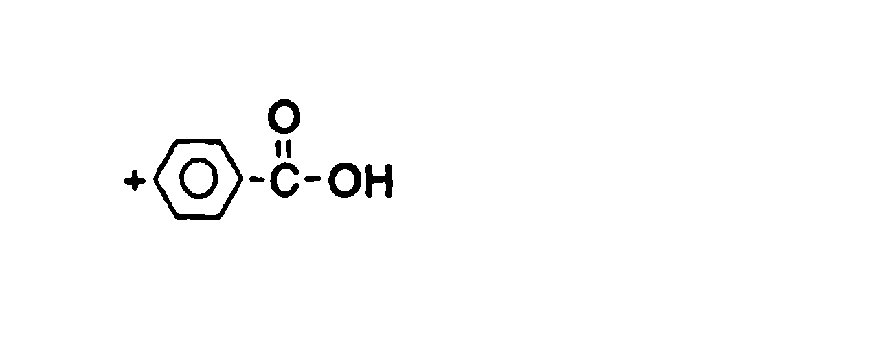
なお、本実施形態の銅張積層体を用いてフレキシブル回路基板を形成する方法としては、上記したセミアディティブ法に限られず、フルアディティブ法やサブトラクティブ法などの他の公知の方法を適用可能である。
なお、スルーホールHの位置や大きさ等は製造するフレキシブル回路基板により適宜決定可能であるため、詳細な説明は省略する。
そこで本発明者らが鋭意検討した結果、上記した加熱(焼鈍)処理を上記したレジストパターニングよりも前に行うことで無電解銅めっき層2における結晶子のサイズを制御し、導電性被膜全体(無電解銅めっき層2および電解銅めっき層3)と低誘電樹脂フィルムとの良好な密着性を確保しつつ無電解銅めっき層2の体積抵抗率を更に良化させることが可能となる。
次に、本実施形態の銅張積層体10の製造方法について図5を用いて説明する。
本実施形態における銅張積層体10の製造方法としては、樹脂フィルム1の少なくとも一方の表面上にカルボキシル基及び/又は水酸基を付与する第1表面改質工程(ステップ1)と、前記カルボキシル基及び/又は水酸基が付与された前記表面に対して湿式方式により電荷を付与する第2表面改質工程(ステップ2)と、前記電荷が付与された前記表面に触媒を吸着させる触媒吸着工程(ステップ3)と、前記触媒が吸着された前記表面に対して無電解銅めっき層2を形成する無電解銅めっき工程(ステップ4)と、前記無電解銅めっき層が形成された前記銅張積層体を加熱する加熱(焼鈍)工程(ステップ5)を含む。
なお後述するとおり、上記ステップ2の第2表面改質工程は、必須ではなく、樹脂フィルム1の材質や第1表面改質工程におけるモル比率などに応じて適宜省略してもよい。
換言すれば、本発明における銅張積層体10の製造方法としては、樹脂フィルム1の少なくとも一方の表面上に対して無電解銅めっき層2を形成する無電解銅めっき工程と、前記無電解銅めっき層が形成された前記銅張積層体をレジストパターニング工程よりも前に加熱する加熱(焼鈍)工程と、を少なくとも含むことになる。
以下、図5も適宜参照しつつ各工程について詳述する。
上記したアルカリは、単独で使用してもよいし、複数を混合して使用してもよい。
モル比率を上記範囲内とすることにより、本発明の目的とする無電解銅めっき層2と樹脂フィルム1との間での粗さ低減(更なる伝送損失の低減)と密着性の両立を達成し得る。その理由は現時点では明らかではないが、発明者らが検討した結果、以下のような理由によるものと推定される。
それ故、本発明者らは、上述したような第1表面改質工程を経ることにより、本発明の目的を達成することに想到したものである。
かような第2表面改質工程は、上記第1表面改質工程において樹脂フィルム1の表面上にカルボキシル基及び/又は水酸基を付与した後に、さらに電荷を付与する工程である。電荷の付与により、樹脂フィルム1と無電解銅めっき層2との密着性を向上させることが可能であるため好ましい。
また、樹脂フィルム1の表面上にマイナス電荷を吸着させる工程においても同様に、公知のアニオン系界面活性剤に浸漬する方法や、スプレー噴霧等の方法を適用することが可能である。
なお、本実施形態の第2表面改質工程は、上述したように湿式方式により行うことが好ましい。湿式で行うことにより、リールtoリール等による大量生産に好適であり、また、低コスト化が可能となるメリットがある。
本実施形態の触媒吸着工程については、上述した第2表面改質工程により表面に少なくともマイナスの電荷が付与された樹脂フィルム1に対して、樹脂フィルム1の表面にさらに触媒を吸着させる工程である。
なお、金属パラジウムの量としては、公知の測定方法により得ることができる。例えば、樹脂フィルム1から銅のみを剥離した後、樹脂フィルム1上のパラジウム残渣を硝酸により溶解し、ICPにより残渣量を測定する等の方法で得ることが可能である。
無電解銅めっき工程は、上記触媒吸着工程を経た後に行われることが好ましい。ここで本実施形態における無電解銅めっき浴としては、EDTA浴、ロッシェル浴、トリエタノールアミン浴などの公知の浴を使用することができる。
以上の工程を経ることで、本実施形態における銅張積層体10が製造される。
なお、樹脂フィルム1のめっき浴への浸漬時間としては、無電解銅めっき層2の厚みが0.1~1.0μmとなるように適宜決定すればよい。
<加熱条件の一例>
加熱温度:150~350℃
加熱(均熱)時間:5~180分
雰囲気:大気中又は不活性ガス(窒素など)中
また、当該加熱(焼鈍)工程を行うことで、無電解銅めっき層2が樹脂フィルム1から剥離することを抑制することができ、無電解銅めっき層2と樹脂フィルム1との密着性も確保することができる。
以上の工程を経ることで、本実施形態における銅張積層体20が製造される。
次に、本実施形態のフレキシブル回路基板について説明する。
本実施形態におけるフレキシブル回路基板は、上述の銅張積層体10の無電解銅めっき層2により回路が形成されてなるフレキシブル回路基板であることが好ましい。
上述したように、本実施形態の銅張積層体10は樹脂フィルム1と無電解銅めっき層2との間の表面粗さRaが所定の値以下であるため、フレキシブル回路基板としての伝送損失を抑制することが可能である。
A≧2.5 ・・・(1)
導体形状の矩形度A=Hw/(Lb-Lt)
配線間距離S≦60μm ・・・(2)
導体配線密度WD≦10.0 ・・・(3)
上記知見の下で本発明者らが鋭意検討した結果、導体形状の矩形度Aの値は2.5以上とし、上記した配線間距離Sが60μm以下とし、且つ、導体配線密度WDが10.0以下とすることが好ましいことに帰結した。これらの値を同時に満たすことで、導体形状の矩形度Aが矩形状である(A≧2.5)と言うことができ、金属配線MWにおける幅方向の断面(導体形状)が実質的に矩形となり、配線抵抗を低下させつつ非矩形状(例えば底辺が比較的大きな台形状など)に比して底面側の鋭角部分が相対的に鈍角化するため、高周波電流などの伝送損失の低下を抑制することが可能となる。
次に本実施形態におけるフレキシブル回路基板100の製造方法について詳述する。以下では、一例として、上記した銅張積層体20を用いて公知のSAP(Semi-Additive Process)法によってフレキシブル回路基板100を製造する場合を説明する。
また、上記した手法でスルーホールHの形成した後で、公知のデスミア処理をしても良い。
なお、この電解銅めっき層3に対しては更なる加熱処理は行わなかった。
浴組成:硫酸銅6水和物 200g/L
硫酸 50g/L
塩化物イオン 50ppm
光沢剤 5ml/L(奥野製薬製添加剤トップルチナ(登録商標))
浴温:20~25℃
電流密度:2.0~3.0A/dm2
また、多層FPC向けの公知の接着層BL(例えば有沢製作所社製のAU、ニッカン工業社製のSAFY、クラレ社製のベクスター(登録商標)CTF、パナソニック社製のR―BM17など、厚みが15μm~25μmの公知のボンディングシート)を用いて、任意のフレキシブル回路基板100を複数積層することで、上記した本実施形態のフレキシブル回路基板200(多層フレキシブル回路基板)を製造できる。
まず樹脂フィルム1として液晶ポリマーフィルム(ベクスターCTQLCP、株式会社クラレ製、厚さ:50μm)を準備した。電気特性としては、10GHzでの比誘電率が3.3、10GHzでの誘電正接が0.002であった。
さらに、触媒吸着工程及び無電解銅めっき工程として、めっき触媒として塩化パラジウム(PdCl2)水溶液(2g/l、pH12、40℃)に5分間浸漬後、浸漬水洗した。さらに、触媒活性剤(還元剤)としてジメチルアミンボラン(DMAB)1g/Lとホウ酸6g/Lを添加した水溶液(25℃)に5分間浸漬後、浸漬水洗した。
浴組成:硫酸銅 7.5g/L
硫酸ニッケル 0.0065g/L
ロッシェル塩 20g/L
水酸化ナトリウム 5g/L
pH:9
浴温:32℃
本実施例では、無電解銅めっき層2を形成した後に、下記条件にてドライオーブン(ヤマト科学社製DY300)を用いて加熱(焼鈍)処理を行った。
<加熱条件>
加熱温度:150℃
加熱(均熱)時間:60分
加熱雰囲気:大気中
電解銅めっき条件としては、以下のとおりとした。
浴組成:硫酸銅6水和物 200g/L
硫酸 50g/L
塩化物イオン 50ppm
光沢剤 5ml/L(奥野製薬製添加剤トップルチナ(登録商標))
浴温:20~25℃
電流密度:2~3A/dm2(本例では2.5A/dm2)
pH:1未満
以上の工程を経ることで、実施例1における銅張積層体20を得た。
<無電解銅めっき層2のNi含有率測定>
表1に示す条件で無電解銅めっき層2を形成後に2cm×2cmを30%硝酸(常温)に浸漬して無電解銅めっき層2を溶解し、得られた液をプラズマ発光分光分析装置(ICP)(島津製作所製ICPE-9820)を用いて、Cu(銅)およびNi(ニッケル)の重量を測定し、Ni重量/Cu重量+Ni重量を算出して無電解銅めっき層2のNi含有率を算出した。
樹脂フィルム1と無電解銅めっき層2の界面におけるカルボキシル基及び/又は水酸基の存在を確認するため、表面状態の確認を行った。
まず、得られた銅張積層体10について、熱処理を行わずに、無電解銅めっき層2を42ボーメのFeCl3溶液(50℃)に浸漬し、無電解銅めっき層2が消えたことを目視で確認したタイミングで取り出すことで無電解銅めっき層2を剥離し、樹脂フィルムを露出させた。露出した樹脂フィルム表面を、20mm×20mmの大きさに切り出して測定サンプルとした。この測定サンプルを、X線光電子分光分析機(日本電子株式会社製、JPS-9200、X線源:Mg、分析領域:φ3mm)で測定し、C1sスペクトルを得た。そして、束縛エネルギー288.8eVに表れるカルボキシル基(COO(H)結合)に由来するピークの強度と束縛エネルギー284.7eVに現れるC-C結合に由来するピークの強度を算出した。
上記ESCAでの測定結果によれば、カルボキシル基の存在が確認できなかった。次いで、TOF-SIMSにより、上記測定サンプルの表面状態を確認した。
一次イオン:69Ga
加速電圧:15kV
測定範囲:100μm×100μm
マスレンジ:0.5~300(m/z)
ESCAでの測定結果によれば、カルボキシル基の存在が確認できなかったことより、第1表面改質工程及び第2表面改質工程を施した後は、C8H9O(-CH-CH3-C6H4-OH)基が導入されたと判断した。
得られた銅張積層体10(無電解銅めっき層の厚さ:表1に示す厚み、電解銅めっき層の厚さ:18μm)に対してFeCl3溶液を用いて無電解銅めっき層2及び電解銅めっき層3を剥離し、樹脂フィルムを露出させた。露出した樹脂フィルムの表面粗さ(Ra)を、レーザー顕微鏡(オリンパス OLS3500)のAFMモード、視野角5μm×5μmにて測定した。得られた値を表2に示す。
得られた銅張積層体10について、前述と同様の方法でFeCl3溶液を用いて無電解銅めっき層2を剥離し、樹脂フィルムを露出させた。露出した樹脂フィルム表面を、20mm×20mmに切り出して測定サンプルとした。このサンプル表面に純水を2.0μL滴下し、接触角を接触角測定器(協和界面科学株式会社製、DropMaster)で測定した。なお、実施例1に使用した未処理の樹脂表面の接触角は、65°であった。
無電解銅めっき層2が形成された銅張積層体10(無電解銅めっき層の厚さ:表1に示す厚み)に対して無電解銅めっき層2の表面に粘着テープ(ニチバン社製)を貼付した後、引き剥がすことによりテープ剥離試験を実施し、目視にて無電解銅めっき層2の剥離が確認されなかった場合には、評価結果を〇とした。結果を表2に示す。
電解銅めっき層3が形成された銅張積層体20を、40mm×40mmの大きさの試片を切り出し、切り出した試片をポリイミドテープでアルミ板に張り付けた。樹脂フィルムと無電解銅めっき層の接着力として90°ピール強度を以下のようにして測定した。
すなわち、各供試材に電解銅めっき層を形成させた面に、5mmの間隔で銅めっき面にカッターで短冊状に切り込みを入れ、次いで短冊状の端部を強制剥離し剥離のきっかけを作り、剥離した樹脂フィルムと銅めっき部を作った。次いで、剥離した樹脂フィルムと銅めっき層をテンシロンのチャックで挟んで、オートグラフにより、90°ピール強度を測定した。なお、90°ピール強度はN/cm(幅)に換算した。これらの結果を表2に示す。
得られた銅張積層体10について、無電解銅めっき層の外観を目視で観察し、剥がれや膨れのないものを○として表2に示した。
得られた銅張積層体10の体積抵抗率(μΩ・cm)を、ロレスターGP(三菱ケミカル社製MCP-T600)を用いて4探針法で測定した。この体積抵抗率の測定結果を表2に示す。
無電解めっきにおける浴組成において硫酸ニッケル(NiSO4)の添加量を0.013g/Lとしたこと以外は、実施例1と同様に行った。なお、得られた無電解Cu-Niめっき層におけるNiの含有率は、0.14wt%であった。また、この無電解銅めっき層の体積抵抗率は、3.82μΩ・cmであった。結果を表1及び表2に示す。
無電解めっきにおける浴組成において硫酸ニッケル(NiSO4)の添加量を0.065g/Lとしたこと以外は、実施例1と同様に行った。なお、得られた無電解Cu-Niめっき層におけるNiの含有率は、0.18wt%であった。また、この無電解銅めっき層の体積抵抗率は、3.85μΩ・cmであった。結果を表1及び表2に示す。
無電解めっきにおける浴組成において硫酸ニッケル(NiSO4)の添加量を0.13g/Lとしたこと以外は、実施例1と同様に行った。なお、得られた無電解Cu-Niめっき層におけるNiの含有率は、0.41wt%であった。また、この無電解銅めっき層の体積抵抗率は、5.66μΩ・cmであった。結果を表1及び表2に示す。
無電解めっきにおける浴組成において硫酸ニッケル(NiSO4)の添加量を0.325g/Lとしたこと以外は、実施例1と同様に行った。なお、得られた無電解Cu-Niめっき層におけるNiの含有率は、0.74wt%であった。また、この無電解銅めっき層の体積抵抗率は、5.98μΩ・cmであった。結果を表1及び表2に示す。
無電解めっきにおける浴組成において硫酸ニッケル(NiSO4)の添加量を0.0065g/Lとしたこと、加熱(焼鈍)工程における雰囲気を不活性ガス(窒素)中とし、真空乾燥装置(佐藤真空社製DQ-46P-LP)を用いて加熱温度を280℃とし、加熱(均熱)時間を180分としたこと以外は、実施例1と同様に行った。なお、得られた無電解Cu-Niめっき層におけるNiの含有率は、0.09wt%であった。また、この無電解銅めっき層の体積抵抗率は、2.3μΩ・cmであった。結果を表1及び表2に示す。
また、本実施例6によって得られた銅張積層体10に対して上述したセミアディティブ法で電解銅めっき層3を形成した配線例の画像を、参考として図6に示す。
無電解めっきにおける浴組成において硫酸ニッケル(NiSO4)の添加量を0.013g/Lとしたこと以外は、実施例6と同様に行った。なお、得られた無電解Cu-Niめっき層におけるNiの含有率は、0.14wt%であった。また、この無電解銅めっき層の体積抵抗率は、2.28μΩ・cmであった。結果を表1及び表2に示す。
無電解めっきにおける浴組成において硫酸ニッケル(NiSO4)の添加量を0.065g/Lとしたこと以外は、実施例6と同様に行った。なお、得られた無電解Cu-Niめっき層におけるNiの含有率は、0.18wt%であった。また、この無電解銅めっき層の体積抵抗率は、2.26μΩ・cmであった。結果を表1及び表2に示す。
無電解めっきにおける浴組成において硫酸ニッケル(NiSO4)の添加量を0.13g/Lとしたこと以外は、実施例6と同様に行った。なお、得られた無電解Cu-Niめっき層におけるNiの含有率は、0.41wt%であった。また、この無電解銅めっき層の体積抵抗率は、4.47μΩ・cmであった。結果を表1及び表2に示す。
無電解めっきにおける浴組成において硫酸ニッケル(NiSO4)の添加量を0.325g/Lとしたこと以外は、実施例6と同様に行った。なお、得られた無電解Cu-Niめっき層におけるNiの含有率は、0.74wt%であった。また、この無電解銅めっき層の体積抵抗率は、4.97μΩ・cmであった。結果を表1及び表2に示す。
無電解めっきにおける浴組成において硫酸ニッケル(NiSO4)の添加量を0.65g/Lとしたこと、無電解めっきのめっき厚を0.3μmとしたこと以外は、実施例6と同様に行った。なお、得られた無電解Cu-Niめっき層におけるNiの含有率は、1.18wt%であった。また、この無電解銅めっき層の体積抵抗率は、5.54μΩ・cmであった。結果を表1及び表2に示す。
樹脂フィルム1を変性ポリイミド(MPI)としたこと、第1表面改質工程として、水酸化カリウム水溶液とモノエタノールアミンの混合液40体積%に水60体積%を更に混合した表面改質用混合液を調製したこと、第2表面改質工程を省略したこと、無電解Cu-Niめっき層2のめっき厚を0.3μmとしたこと、加熱(焼鈍)工程における加熱温度を220℃として加熱(均熱)時間を30分としたこと以外は、実施例8と同様に行った。
加熱(焼鈍)工程における加熱温度を300℃とし、加熱(均熱)時間を60分としたこと以外は、実施例12と同様に行った。結果を表1及び表2に示す。
FCCL(フレキシブル銅張積層体)として、上記した実施例6で製造した銅張積層体20を用いた。
この銅張積層体20に対して公知のロールラミネータにより、公知のDFR(ドライフィルムレジスト)を貼りあわせた。次いで所定のレジストパターン画像が形成されたマスクを介して公知の露光装置により紫外線露光することでレジスト中のネガ部分を硬化させた。
次いで、下記で示されるめっき条件により、レジストパターンが形成された無電解銅めっき層上に、表3に記載の所定の配線高さHwとなるように電解銅めっきを形成した。
浴組成:硫酸銅6水和物 70g/L
98%硫酸 200g/L
35%塩酸 0.15ml/L
添加剤 奥野製薬製トップルチナ(登録商標)SFベースWR2.5ml/L、
トップルチナ(登録商標)SF-B1.0ml/L、および、
トップルチナ(登録商標)SFレベラー5.0ml/L
浴温:25℃
電流密度(陰極):3.0A/dm2
浴組成:35%過酸化水素 4.5容量%、
98%硫酸 5容量%、
硫酸銅・5水和物 30g/L
すなわち、まず上記した電子顕微鏡で得られた断面写真に対し、金属配線の底辺、上辺、および両側面にそれぞれ接線を引く。そしてこの接線を基準として、底辺の幅Lb及び上面の幅Ltについては、両側面の接線と接線の交点間距離を、電子顕微鏡での画像中に表示されるスケールを基に測定する。また、配線高さHwについては、上記した底辺の幅Lbの中点(1/2の点)から上辺と交わるように垂直に線を引いたとき、その上辺との交点と上記底辺の中点との間の距離を、電子顕微鏡での画像中に表示されるスケールを基に測定する。
得られた結果を表3に示す。
表3に記載の底辺幅Lbと配線間距離Sとなるように設計された露光用のフォトマスクに変更したこと以外は、実施例14と同様に行った。得られた結果を表3に示す。また、得られたフレキシブル回路基板の一部(金属配線の一例)を図8に示す。
FCCL(フレキシブル銅張積層体)として上記した実施例8で製造した銅張積層体20を用いたこと、表3に記載の底辺幅Lbと配線間距離Sとなるように設計された露光用のフォトマスクに変更したこと以外は、実施例15と同様に行った。得られた結果を表3に示す。なお、この実施例17で得られたフレキシブル回路基板の金属配線MWのうち、底辺の幅Lbと上面の幅Ltの差(Lb-Lt)は、ほぼ0(ゼロ)となった。従って、本実施例における導体形状の矩形度Aはほぼ無限大(∞)となることから「∞」と見做し、導体配線密度WDもほぼゼロ(0)となることから「0」と見做した。
表3に記載の底辺幅Lbと配線間距離Sとなるように設計された露光用のフォトマスクに変更したこと以外は、実施例16と同様に行った。得られた結果を表3に示す。
表3に記載の底辺幅Lbと配線間距離Sとなるように設計された露光用のフォトマスクに変更したこと以外は、実施例16と同様に行った。得られた結果を表3に示す。
無電解めっき浴調整後、無電解めっき浴に重量平均分子量1,000のポリエチレングリコールを0.8g/lの濃度になるように添加したこと、加熱温度を250℃とし、加熱(均熱)時間を30分としたこと、無電解めっきのめっき厚を0.3μmとしたこと以外は、実施例8と同様に行った。結果を表1及び表2に示す。
無電解めっき浴調整後、無電解めっき浴に重量平均分子量1,000のポリエチレングリコールを1.0g/lの濃度になるように添加したこと以外は、実施例19と同様に行った。結果を表1及び表2に示す。
第1表面改質工程として水酸化カリウム水溶液とモノエタノールアミンの混合液20体積%に対して水80体積%を混合することで第1表面改質用の混合液を調製したこと、第2表面改質を実施したこと、無電解Cu-Niめっき層2のめっき厚を0.1μmとしたこと、加熱(焼鈍)工程における加熱温度を250℃とし、加熱(均熱)時間を30分、としたこと以外は、実施例12と同様に行った。結果を表1及び表2に示す。
第1表面改質工程として水酸化カリウム水溶液とモノエタノールアミンの混合液15体積%に対して水85体積%を混合することで第1表面改質用の混合液を調製したこと、第2表面改質を実施したこと、無電解Cu-Niめっき層2のめっき厚を0.1μmとしたこと、加熱(焼鈍)工程における加熱温度を250℃とし、加熱(均熱)時間を30分、としたこと以外は、実施例12と同様に行った。結果を表1及び表2に示す。
FCCL(フレキシブル銅張積層体)として上記した実施例21で製造した銅張積層体20を用いたこと、表3に記載の底辺幅Lbと配線間距離Sとなるように設計された露光用のフォトマスクに変更したこと以外は、実施例14と同様に行った。得られた結果を表3に示す。
配線高さHwを12μm、L/S(Line&Spaceであり本実施例ではLb/Sに相当)として20μm/20μmにしたこと以外は、実施例14と同様にして、金属配線のパターンを両面に形成したフレキシブル回路基板(FPC)を作製した。この基板をコア層に用いる。
本実施例で得られた4層フレキシブル回路基板の一部の断面画像(電子顕微鏡で撮影)を図10に示す。
無電解めっきにおける条件を下記としたこと以外は、実施例1と同様に行った。すなわち、本比較例1では、硫酸ニッケル(NiSO4)の添加量を0として無電解Cuめっきとした。
[無電解めっき条件]
浴組成:硫酸銅 7.5g/L
ロッシェル塩 20g/L
水酸化ナトリウム 5g/L
pH:9
浴温:32℃
無電解めっきにおけるめっき厚を0.3μmとしたこと、加熱(焼鈍)工程における雰囲気を大気中とし、実施例1で使用した装置を用いて加熱温度を150℃とし、加熱(均熱)時間を60分としたこと以外は、実施例11と同様に行った。なお、得られた無電解Cu-Niめっき層におけるNiの含有率は、1.18wt%であった。また、この無電解銅めっき層の体積抵抗率は、6.89μΩ・cmとなって6.0μΩ・cmを超える結果であった。結果を表1及び表2に示す。
加熱(焼鈍)工程における雰囲気を不活性ガス(窒素)中とし、実施例6で使用した装置を用いて加熱温度を280℃とし、加熱(均熱)時間を180分としたこと以外は、比較例1と同様に行った。比較例1と同様に、本比較例3においても不めっき箇所が多発した。なお、比較例1と同様にして得られた無電解銅めっき層におけるNiの含有率は、0wt%であった。また、この無電解銅めっき層の体積抵抗率は、2.29μΩ・cmであった。結果を表1及び表2に示す。
FCCL(フレキシブル銅張積層体)として、市販の銅張積層体を準備した。このFCCLの液晶ポリマーフィルムの厚みは50μmであり、電解銅箔の厚みは18μmであった。この準備したFCCLに対し、公知の手法で金属配線の厚み(配線高さHw)が30μmとなるように電解銅めっきを施した。
以上により比較例2のフレキシブル回路基板(FPC)を得た。得られたFPCにおける金属配線の諸元を表3に示す。また、得られたフレキシブル回路基板の一部(金属配線の一例)を図9(a)に示す。
銅張積層板として、液晶ポリマーフィルム50μm、圧延銅箔18μmを用いたこと、電解銅めっき後の金属配線の厚み(配線高さHw)を29.2μmとしたこと以外は、比較例2と同様に行った。結果を表3に示す。また、得られたフレキシブル回路基板の一部(金属配線の一例)を図9(b)に示す。
市販のスマートフォンを準備し、分解することで搭載されているフレキシブル回路基板を取り出した。このフレキシブル回路基板は、基材樹脂に液晶ポリマーを用いており5層積層構造を有していた。このフレキシブルプリント基板の金属配線の諸元を実施例17と同様に調査した。結果を表3に示す。
比較例4で得られたフレキシブルプリント基板、別の部位の金属配線の諸元を実施例17と同様に調査した。結果を表3に示す。

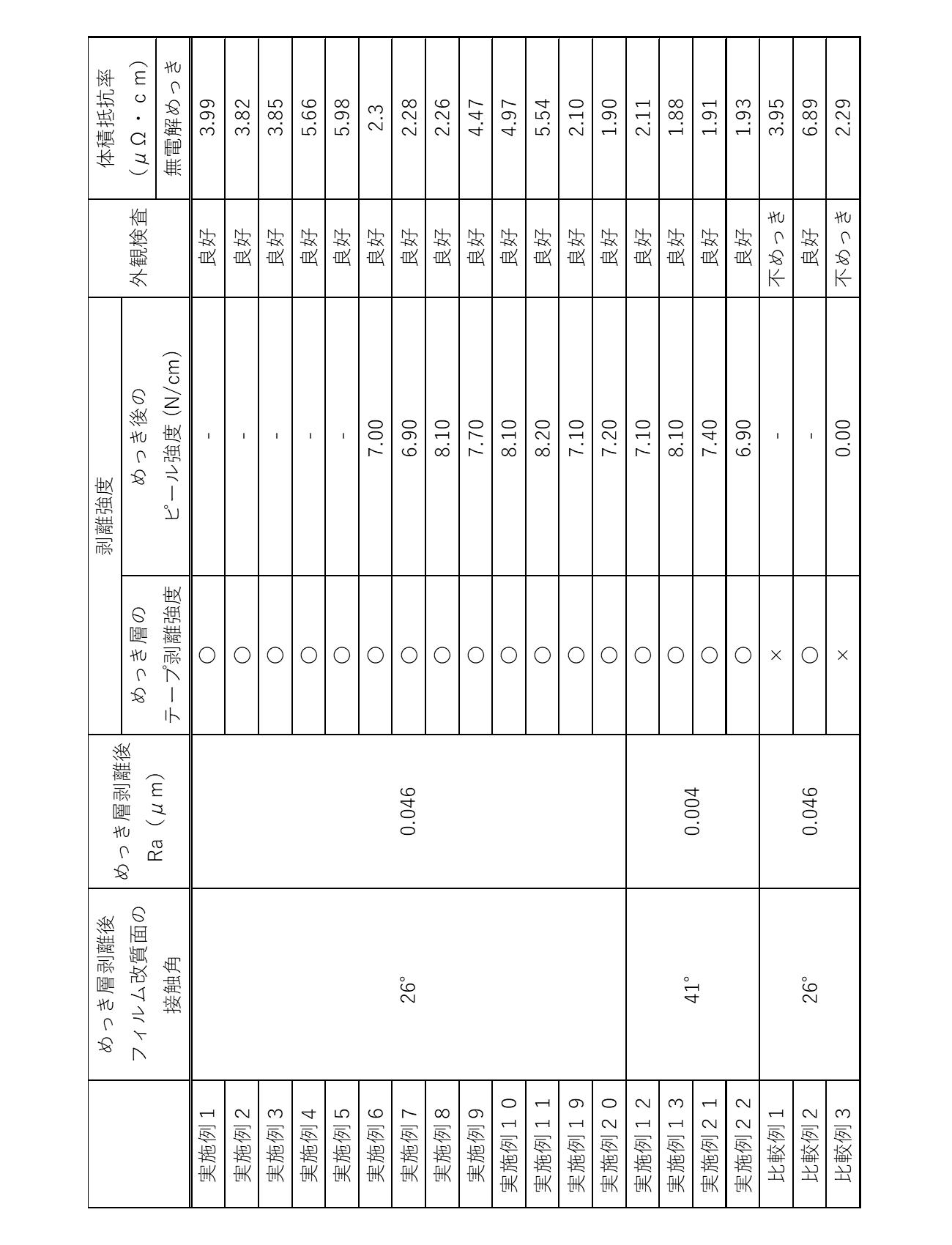
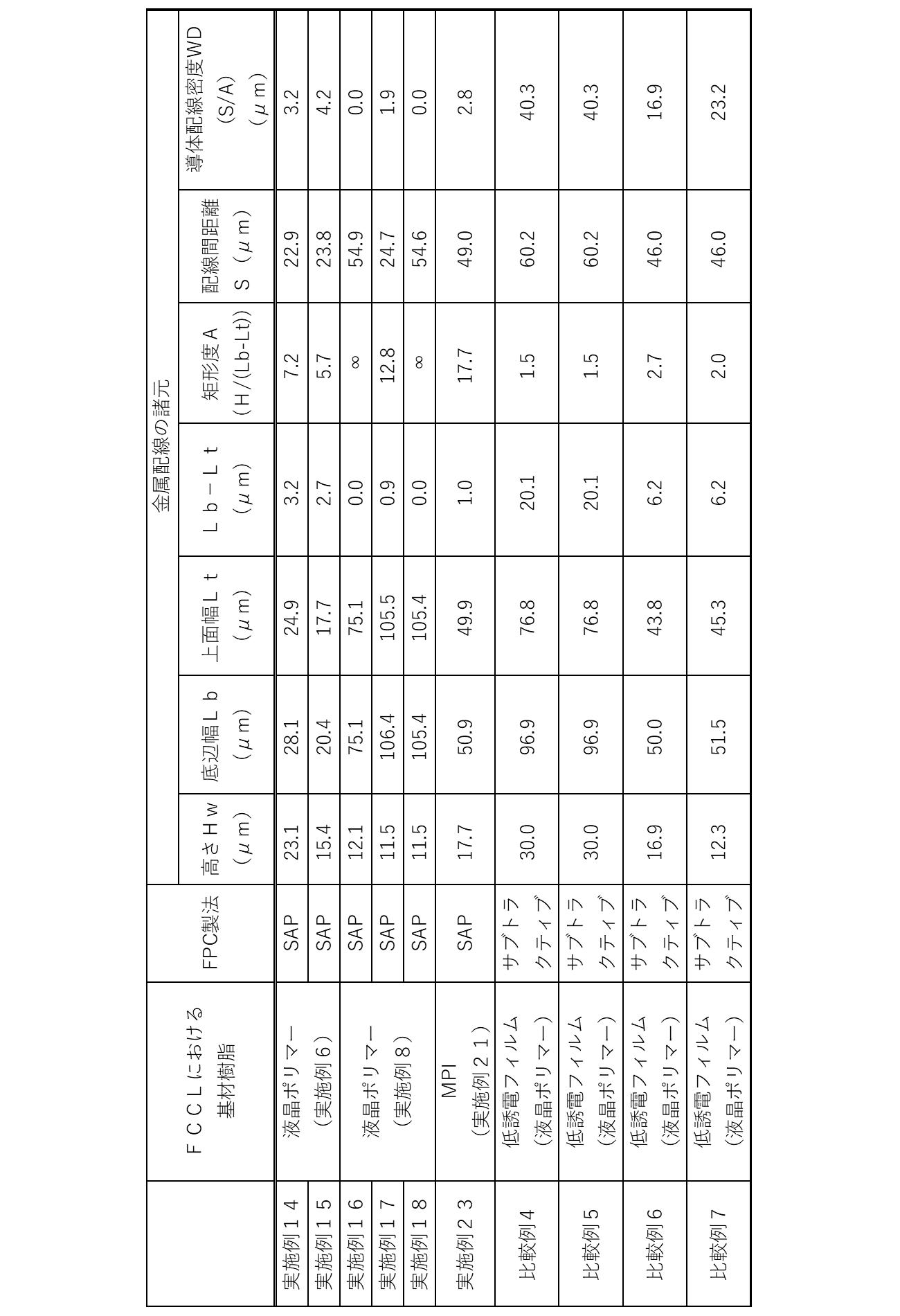
2 無電解銅めっき層
3 電解銅めっき層
10 銅張積層体
Claims (13)
- 周波数10GHzにおける比誘電率が3.5以下、且つ誘電正接が0.008以下である低誘電樹脂フィルムと、
前記低誘電樹脂フィルムの少なくとも一方の面に積層された無電解銅めっき層と、
を含み、
前記無電解銅めっき層におけるNi含有率が0.01~1.2wt%であり、且つ、前記無電解銅めっき層の体積抵抗率が6.0μΩ・cm以下であることを特徴とする銅張積層体。 - 前記樹脂フィルムと前記無電解銅めっき層との密着強度が4.2N/cm以上である、請求項1に記載の銅張積層体。
- 前記無電解銅めっき層上に電解銅めっき層を備え、
前記電解銅めっき層における体積抵抗率が5.0μΩ・cm以下である、請求項1又は2に記載の銅張積層体。 - 前記無電解銅めっき層におけるNi含有率が0.01~1.0wt%である、請求項1~3のいずれか一項に記載の銅張積層体。
- 前記低誘電樹脂フィルムが、ポリイミド、変性ポリイミド、液晶ポリマー、フッ素系樹脂の何れか、もしくはその混成物である、請求項1~4のいずれか一項に記載の銅張積層体。
- 前記低誘電樹脂フィルムのうち前記無電解銅めっき層と接するめっき層側界面における平均表面粗さRaが1~150nmであり、前記樹脂フィルムのめっき層側界面における飛行時間型質量分析法(TOF-SIMS)による質量121の強度が800以上であり、且つ、前記樹脂フィルムのめっき層側界面は水酸基及び/又はカルボキシル基が付与されている、請求項1~5のいずれか一項に記載の銅張積層体。
- 周波数10GHzにおける比誘電率が3.5以下、且つ、誘電正接が0.008以下である低誘電樹脂フィルムに無電解銅めっき層を形成して製造される銅張積層体の製造方法であって、
前記無電解銅めっき層におけるNi含有率が0.01~1.2wt%であり且つ前記無電解銅めっき層の体積抵抗率が6.0μΩ・cm以下となるように前記低誘電樹脂フィルムの表面に対して無電解銅めっき層を形成する無電解銅めっき工程を含むことを特徴とする銅張積層体の製造方法。 - 前記無電解銅めっき工程の後に前記無電解銅めっき層を加熱する加熱工程をさらに有し、
前記加熱工程では、(i)大気中においては150~200℃で10~180分、及び(ii)不活性ガス中においては150~350℃で5~180分、のいずれかの加熱条件で前記銅張積層体が加熱される、請求項7に記載の銅張積層体の製造方法。 - 前記加熱工程は、前記無電解銅めっき層上へのレジストパターニング工程よりも前に行われる、請求項7又は8に記載の銅張積層体の製造方法。
- 前記無電解銅めっき工程よりも前に、
前記低誘電樹脂フィルムの表面にカルボキシル基及び/又は水酸基を付与する第1表面改質工程と、
前記カルボキシル基及び/又は水酸基が付与された前記表面に対して湿式方式により電荷を付与する第2表面改質工程と、
前記電荷が付与された前記表面に触媒を吸着させる触媒吸着工程と、をさらに有し、
前記触媒が吸着された前記表面に対して前記無電解銅めっき層が形成される、請求項7~9のいずれか一項に記載の銅張積層体の製造方法。 - 請求項1~6のいずれか一項に記載された銅張積層体による回路が形成されたフレキシブル回路基板。
- 前記銅張積層体による前記低誘電樹脂フィルム上に形成された金属配線の前記回路を有し、
前記金属配線の少なくとも一部は、前記低誘電樹脂フィルムからの配線高さをHw、前記低誘電フィルムと接する底辺の幅をLb、上面の幅をLt、前記低誘電樹脂フィルム上において隣り合う他の金属配線との配線間距離をSとしたとき、
前記配線高さを前記底辺の幅と前記上面の幅の差で除した値(Hw/(Lb-Lt))で規定される前記金属配線における導体形状の矩形度Aが2.5以上であり、
Sが60μm以下であり、且つ、
前記配線間距離を前記導体形状の矩形度で除した値(S/A)で規定される導体配線密度WDが10.0以下である、
ことを特徴とする請求項11に記載のフレキシブル回路基板。 - 前記金属配線を含む導体層を有して少なくとも4層以上積層されてなり、
全体の厚みを前記導体層の層数で除した平均厚みが50μm以下である、
請求項12に記載のフレキシブル回路基板。
Priority Applications (6)
| Application Number | Priority Date | Filing Date | Title |
|---|---|---|---|
| KR1020237001503A KR20230049080A (ko) | 2020-08-07 | 2021-08-07 | 동장 적층체 및 그 제조 방법 |
| US18/040,214 US12402253B2 (en) | 2020-08-07 | 2021-08-07 | Copper clad laminate and method for producing the same |
| JP2022541767A JP7738563B2 (ja) | 2020-08-07 | 2021-08-07 | 銅張積層体及びその製造方法 |
| CN202180057458.9A CN116057205A (zh) | 2020-08-07 | 2021-08-07 | 覆铜层叠体及其制造方法 |
| US19/277,029 US20250351274A1 (en) | 2020-08-07 | 2025-07-22 | Copper clad laminate and method for producing the same |
| JP2025145167A JP2025183256A (ja) | 2020-08-07 | 2025-09-02 | 銅張積層体及びその製造方法 |
Applications Claiming Priority (4)
| Application Number | Priority Date | Filing Date | Title |
|---|---|---|---|
| JP2020-134876 | 2020-08-07 | ||
| JP2020134876 | 2020-08-07 | ||
| JP2021-093954 | 2021-06-03 | ||
| JP2021093954 | 2021-06-03 |
Related Child Applications (2)
| Application Number | Title | Priority Date | Filing Date |
|---|---|---|---|
| US18/040,214 A-371-Of-International US12402253B2 (en) | 2020-08-07 | 2021-08-07 | Copper clad laminate and method for producing the same |
| US19/277,029 Continuation US20250351274A1 (en) | 2020-08-07 | 2025-07-22 | Copper clad laminate and method for producing the same |
Publications (1)
| Publication Number | Publication Date |
|---|---|
| WO2022030645A1 true WO2022030645A1 (ja) | 2022-02-10 |
Family
ID=80117555
Family Applications (1)
| Application Number | Title | Priority Date | Filing Date |
|---|---|---|---|
| PCT/JP2021/029462 Ceased WO2022030645A1 (ja) | 2020-08-07 | 2021-08-07 | 銅張積層体及びその製造方法 |
Country Status (5)
| Country | Link |
|---|---|
| US (2) | US12402253B2 (ja) |
| JP (2) | JP7738563B2 (ja) |
| KR (1) | KR20230049080A (ja) |
| CN (1) | CN116057205A (ja) |
| WO (1) | WO2022030645A1 (ja) |
Cited By (1)
| Publication number | Priority date | Publication date | Assignee | Title |
|---|---|---|---|---|
| CN119571426A (zh) * | 2025-02-07 | 2025-03-07 | 昆山科比精工设备有限公司 | 一种真空蒸镀基膜的复合铜箔制作装置及方法 |
Citations (8)
| Publication number | Priority date | Publication date | Assignee | Title |
|---|---|---|---|---|
| JPS5229970B2 (ja) * | 1973-02-12 | 1977-08-05 | ||
| JP2001020077A (ja) * | 1999-07-07 | 2001-01-23 | Sony Corp | 無電解めっき方法及び無電解めっき液 |
| JP2002093747A (ja) * | 2000-09-19 | 2002-03-29 | Sony Corp | 導体構造の形成方法及び導体構造、並びに半導体装置の製造方法及び半導体装置 |
| JP2002256443A (ja) * | 2001-02-27 | 2002-09-11 | Japan Science & Technology Corp | メッキ方法 |
| JP2003013247A (ja) * | 2001-04-24 | 2003-01-15 | Murata Mfg Co Ltd | 無電解銅めっき浴及び高周波用電子部品 |
| JP2005171287A (ja) * | 2003-12-09 | 2005-06-30 | Murata Mfg Co Ltd | 無電解銅めっき浴、および高周波用電子部品 |
| JP2007154306A (ja) * | 2005-11-14 | 2007-06-21 | Fujifilm Corp | 金属膜形成方法、金属膜形成用基板、金属膜、金属パターン形成方法、金属パターン形成用基板、金属パターン、及びポリマー層形成用組成物 |
| JP2007305660A (ja) * | 2006-05-09 | 2007-11-22 | Alps Electric Co Ltd | めっき配線基板およびめっき配線基板の製造方法 |
Family Cites Families (17)
| Publication number | Priority date | Publication date | Assignee | Title |
|---|---|---|---|---|
| JPS5229970A (en) * | 1975-09-01 | 1977-03-07 | Fujitsu Ltd | Printed circuit substrate stack structure |
| SE454960B (sv) | 1982-06-02 | 1988-06-13 | N Proizv Ob Po Tech Masch | Anordning for styrning av ett huvud hos en svetsautomat lengs arbetsstyckets yta |
| JP2003001756A (ja) | 2001-06-27 | 2003-01-08 | Oike Ind Co Ltd | 銅薄膜積層体 |
| JP2007262493A (ja) | 2006-03-28 | 2007-10-11 | Toray Advanced Film Co Ltd | フレキシブルプリント基板用材料およびその製造方法 |
| JP5149805B2 (ja) * | 2006-11-06 | 2013-02-20 | アルプス電気株式会社 | 無電解銅めっき方法 |
| JP2008186970A (ja) * | 2007-01-30 | 2008-08-14 | Sumitomo Metal Mining Co Ltd | フレキシブル配線板用基板とその製造方法、同基板を用いたフレキシブル配線板 |
| JP2009043800A (ja) * | 2007-08-07 | 2009-02-26 | Sumitomo Metal Mining Co Ltd | フレキシブル配線用基板 |
| JP5186266B2 (ja) | 2008-03-31 | 2013-04-17 | 新日鉄住金化学株式会社 | 多層配線回路基板及びその製造方法 |
| JP2009274250A (ja) | 2008-05-13 | 2009-11-26 | Sumitomo Metal Mining Co Ltd | 金属被覆ポリイミドフィルム基板 |
| JP2012015448A (ja) * | 2010-07-05 | 2012-01-19 | Teraoka Seisakusho:Kk | フレキシブル銅張積層板及びその製造方法並びにそれを用いた配線基板 |
| JP2012023296A (ja) | 2010-07-16 | 2012-02-02 | Dainippon Printing Co Ltd | 回路基板、回路基板の製造方法、サスペンション用基板、サスペンション、素子付サスペンションおよびハードディスクドライブ |
| JP5022501B2 (ja) | 2010-11-04 | 2012-09-12 | 株式会社日本表面処理研究所 | 成形回路部品の製造方法 |
| CN102400115B (zh) * | 2011-10-20 | 2014-04-02 | 复旦大学 | 一种微米级线宽的柔性铜电极图形的制备方法 |
| JP6202905B2 (ja) | 2013-06-27 | 2017-09-27 | 株式会社クラレ | 回路基板およびその製造方法 |
| JP6264900B2 (ja) * | 2014-01-24 | 2018-01-24 | 日立化成株式会社 | レジストパターンの製造方法、配線パターンの製造方法及び配線基板 |
| CN104582298A (zh) * | 2014-12-25 | 2015-04-29 | 复旦大学 | 一种在纸质基材上制作导电电路的方法 |
| EP3683050A4 (en) * | 2017-09-15 | 2021-06-23 | JSR Corporation | HIGH FREQUENCY CIRCUIT LAMINATE, MANUFACTURING METHOD FOR IT AND B-STAGE FILM |
-
2021
- 2021-08-07 JP JP2022541767A patent/JP7738563B2/ja active Active
- 2021-08-07 WO PCT/JP2021/029462 patent/WO2022030645A1/ja not_active Ceased
- 2021-08-07 CN CN202180057458.9A patent/CN116057205A/zh active Pending
- 2021-08-07 KR KR1020237001503A patent/KR20230049080A/ko active Pending
- 2021-08-07 US US18/040,214 patent/US12402253B2/en active Active
-
2025
- 2025-07-22 US US19/277,029 patent/US20250351274A1/en active Pending
- 2025-09-02 JP JP2025145167A patent/JP2025183256A/ja active Pending
Patent Citations (8)
| Publication number | Priority date | Publication date | Assignee | Title |
|---|---|---|---|---|
| JPS5229970B2 (ja) * | 1973-02-12 | 1977-08-05 | ||
| JP2001020077A (ja) * | 1999-07-07 | 2001-01-23 | Sony Corp | 無電解めっき方法及び無電解めっき液 |
| JP2002093747A (ja) * | 2000-09-19 | 2002-03-29 | Sony Corp | 導体構造の形成方法及び導体構造、並びに半導体装置の製造方法及び半導体装置 |
| JP2002256443A (ja) * | 2001-02-27 | 2002-09-11 | Japan Science & Technology Corp | メッキ方法 |
| JP2003013247A (ja) * | 2001-04-24 | 2003-01-15 | Murata Mfg Co Ltd | 無電解銅めっき浴及び高周波用電子部品 |
| JP2005171287A (ja) * | 2003-12-09 | 2005-06-30 | Murata Mfg Co Ltd | 無電解銅めっき浴、および高周波用電子部品 |
| JP2007154306A (ja) * | 2005-11-14 | 2007-06-21 | Fujifilm Corp | 金属膜形成方法、金属膜形成用基板、金属膜、金属パターン形成方法、金属パターン形成用基板、金属パターン、及びポリマー層形成用組成物 |
| JP2007305660A (ja) * | 2006-05-09 | 2007-11-22 | Alps Electric Co Ltd | めっき配線基板およびめっき配線基板の製造方法 |
Cited By (1)
| Publication number | Priority date | Publication date | Assignee | Title |
|---|---|---|---|---|
| CN119571426A (zh) * | 2025-02-07 | 2025-03-07 | 昆山科比精工设备有限公司 | 一种真空蒸镀基膜的复合铜箔制作装置及方法 |
Also Published As
| Publication number | Publication date |
|---|---|
| CN116057205A (zh) | 2023-05-02 |
| US20250351274A1 (en) | 2025-11-13 |
| JP7738563B2 (ja) | 2025-09-12 |
| US12402253B2 (en) | 2025-08-26 |
| JPWO2022030645A1 (ja) | 2022-02-10 |
| JP2025183256A (ja) | 2025-12-16 |
| TW202214051A (zh) | 2022-04-01 |
| US20230269880A1 (en) | 2023-08-24 |
| KR20230049080A (ko) | 2023-04-12 |
Similar Documents
| Publication | Publication Date | Title |
|---|---|---|
| TWI699459B (zh) | 表面處理銅箔及使用其之積層板、附載體銅箔、印刷配線板、電子機器、以及印刷配線板之製造方法 | |
| KR101830994B1 (ko) | 조화처리된 동박, 그 제조방법, 동박 적층판 및 인쇄회로기판 | |
| JP2025183255A (ja) | 銅張積層体及びその製造方法 | |
| JP7849440B2 (ja) | 銅張積層体及びその製造方法 | |
| JP6261037B2 (ja) | 高周波回路用銅箔、銅張積層板及びプリント配線板 | |
| US11770904B2 (en) | Surface-treated copper foil, and copper-clad laminate plate, resin-attached copper foil and circuit board each using same | |
| JP2025183256A (ja) | 銅張積層体及びその製造方法 | |
| US12063747B2 (en) | Surface-treated copper foil, copper-clad laminate and printed wiring board using the surface-treated copper foil | |
| TWI916388B (zh) | 鍍銅積層體及其製造方法、以及可撓性電路基板 | |
| TWI920122B (zh) | 鍍銅積層體及其製造方法 | |
| JP6827083B2 (ja) | 表面処理銅箔、銅張積層板、及びプリント配線板 | |
| JP2025040846A (ja) | 銅張積層体及びその製造方法 |
Legal Events
| Date | Code | Title | Description |
|---|---|---|---|
| 121 | Ep: the epo has been informed by wipo that ep was designated in this application |
Ref document number: 21852779 Country of ref document: EP Kind code of ref document: A1 |
|
| ENP | Entry into the national phase |
Ref document number: 2022541767 Country of ref document: JP Kind code of ref document: A |
|
| NENP | Non-entry into the national phase |
Ref country code: DE |
|
| 122 | Ep: pct application non-entry in european phase |
Ref document number: 21852779 Country of ref document: EP Kind code of ref document: A1 |
|
| WWG | Wipo information: grant in national office |
Ref document number: 18040214 Country of ref document: US |