WO2022014567A1 - 防汚層付き光学フィルム - Google Patents
防汚層付き光学フィルム Download PDFInfo
- Publication number
- WO2022014567A1 WO2022014567A1 PCT/JP2021/026245 JP2021026245W WO2022014567A1 WO 2022014567 A1 WO2022014567 A1 WO 2022014567A1 JP 2021026245 W JP2021026245 W JP 2021026245W WO 2022014567 A1 WO2022014567 A1 WO 2022014567A1
- Authority
- WO
- WIPO (PCT)
- Prior art keywords
- layer
- optical film
- refractive index
- film
- antifouling
- Prior art date
- Legal status (The legal status is an assumption and is not a legal conclusion. Google has not performed a legal analysis and makes no representation as to the accuracy of the status listed.)
- Ceased
Links
Images
Classifications
-
- B—PERFORMING OPERATIONS; TRANSPORTING
- B32—LAYERED PRODUCTS
- B32B—LAYERED PRODUCTS, i.e. PRODUCTS BUILT-UP OF STRATA OF FLAT OR NON-FLAT, e.g. CELLULAR OR HONEYCOMB, FORM
- B32B27/00—Layered products comprising a layer of synthetic resin
-
- B—PERFORMING OPERATIONS; TRANSPORTING
- B32—LAYERED PRODUCTS
- B32B—LAYERED PRODUCTS, i.e. PRODUCTS BUILT-UP OF STRATA OF FLAT OR NON-FLAT, e.g. CELLULAR OR HONEYCOMB, FORM
- B32B7/00—Layered products characterised by the relation between layers; Layered products characterised by the relative orientation of features between layers, or by the relative values of a measurable parameter between layers, i.e. products comprising layers having different physical, chemical or physicochemical properties; Layered products characterised by the interconnection of layers
- B32B7/02—Physical, chemical or physicochemical properties
- B32B7/023—Optical properties
-
- C—CHEMISTRY; METALLURGY
- C23—COATING METALLIC MATERIAL; COATING MATERIAL WITH METALLIC MATERIAL; CHEMICAL SURFACE TREATMENT; DIFFUSION TREATMENT OF METALLIC MATERIAL; COATING BY VACUUM EVAPORATION, BY SPUTTERING, BY ION IMPLANTATION OR BY CHEMICAL VAPOUR DEPOSITION, IN GENERAL; INHIBITING CORROSION OF METALLIC MATERIAL OR INCRUSTATION IN GENERAL
- C23C—COATING METALLIC MATERIAL; COATING MATERIAL WITH METALLIC MATERIAL; SURFACE TREATMENT OF METALLIC MATERIAL BY DIFFUSION INTO THE SURFACE, BY CHEMICAL CONVERSION OR SUBSTITUTION; COATING BY VACUUM EVAPORATION, BY SPUTTERING, BY ION IMPLANTATION OR BY CHEMICAL VAPOUR DEPOSITION, IN GENERAL
- C23C14/00—Coating by vacuum evaporation, by sputtering or by ion implantation of the coating forming material
- C23C14/06—Coating by vacuum evaporation, by sputtering or by ion implantation of the coating forming material characterised by the coating material
-
- G—PHYSICS
- G02—OPTICS
- G02B—OPTICAL ELEMENTS, SYSTEMS OR APPARATUS
- G02B1/00—Optical elements characterised by the material of which they are made; Optical coatings for optical elements
- G02B1/10—Optical coatings produced by application to, or surface treatment of, optical elements
- G02B1/11—Anti-reflection coatings
- G02B1/113—Anti-reflection coatings using inorganic layer materials only
-
- G—PHYSICS
- G02—OPTICS
- G02B—OPTICAL ELEMENTS, SYSTEMS OR APPARATUS
- G02B1/00—Optical elements characterised by the material of which they are made; Optical coatings for optical elements
- G02B1/10—Optical coatings produced by application to, or surface treatment of, optical elements
- G02B1/18—Coatings for keeping optical surfaces clean, e.g. hydrophobic or photo-catalytic films
Definitions
- the present invention relates to an optical film with an antifouling layer.
- a transparent optical film provided with a layer having a predetermined optical function (optical functional layer) is provided.
- the optical film include an antireflection film, a transparent conductive film, and an electromagnetic wave shielding film.
- the optical film includes, for example, a transparent base material, an optical functional layer arranged on one side thereof, and an adhesive layer arranged on the other side of the transparent base material. A technique relating to such an optical film is described in, for example, Patent Document 1 below.
- the optical film in which the optical functional layer is arranged as the outermost layer, contaminants such as hand grease are likely to adhere to the optical functional layer, and the adhered contaminants are difficult to be removed from the optical functional layer. Adhesion of contaminants on the optical film is not preferable from the viewpoint of ensuring the transparency of the optical film. Therefore, for example, the optical film is provided with an antifouling layer as the outermost layer. In such an optical film with an antifouling layer, high antifouling property is required in the antifouling layer.
- the present invention provides an optical film with an antifouling layer suitable for achieving high antifouling properties in the antifouling layer.
- the present invention [1] includes a transparent base material, an optical functional layer, and an antifouling layer in this order, and the outer surface of the antifouling layer on the opposite side of the optical functional layer has a water contact angle of 110 ° or more. Includes an optical film with an antifouling layer.
- the present invention [2] includes the optical film with an antifouling layer according to the above [1], wherein the outer surface has a surface roughness Ra of more than 2 nm.
- the present invention [3] includes the optical film with an antifouling layer according to the above [1] or [2], wherein the optical functional layer is an antireflection layer.
- the antireflection layer according to the above [3], wherein the antireflection layer alternately includes a high refractive index layer having a relatively large refractive index and a low refractive index layer having a relatively small refractive index. includes an optical film with a foul layer.
- the present invention [5] includes the optical film with an antifouling layer according to any one of the above [1] to [4], wherein the transparent substrate has a hard coat layer on the optical functional layer side.
- the present invention [6] includes the optical film with an antifouling layer according to the above [5], wherein the hard coat layer contains metal oxide fine particles.
- the present invention [7] includes the optical film with an antifouling layer according to the above [6], wherein the metal oxide fine particles are nanosilica particles.
- the protection according to any one of the above [5] to [7], wherein the surface of the hard coat layer on the optical functional layer side has a surface roughness Ra of 0.5 nm or more and 20 nm or less. includes an optical film with a dirty layer.
- the optical film with an antifouling layer of the present invention realizes high antifouling property in the antifouling layer because the outer surface of the antifouling layer opposite to the optical functional layer has a water contact angle of 110 ° or more. Suitable for.
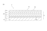
- the optical film F as an embodiment of the optical film with an antifouling layer of the present invention comprises a transparent base material 10, an optical functional layer 20, and an antifouling layer 30 in a thickness direction D. Prepare in this order toward one side.
- the optical film F is preferably provided with the transparent base material 10, the adhesion layer 40, the optical functional layer 20, and the antifouling layer 30 in this order toward one side in the thickness direction D. Is composed of a transparent base material 10, an adhesion layer 40, an optical functional layer 20, and an antifouling layer 30.
- the optical film F has a shape that spreads in a direction (plane direction) orthogonal to the thickness direction D.
- the transparent base material 10 is provided with the resin film 11 and the hard coat layer 12 in this order toward one side in the thickness direction D.
- the resin film 11 is a transparent resin film having flexibility.
- the material of the resin film 11 include polyester resin, polyolefin resin, polystyrene resin, acrylic resin, polycarbonate resin, polyether sulfone resin, polysulfone resin, polyamide resin, polyimide resin, cellulose resin, norbornene resin, polyarylate resin, and Polyvinyl alcohol resin can be mentioned.
- the polyester resin include polyethylene terephthalate (PET), polybutylene terephthalate, and polyethylene naphthalate.
- the polyolefin resin include polyethylene, polypropylene, and cycloolefin polymers.
- the cellulose resin include triacetyl cellulose. These materials may be used alone or in combination of two or more. From the viewpoint of transparency and strength, cellulose resin is preferably used as the material of the resin film 11, and triacetyl cellulose is more preferably used.
- the surface of the resin film 11 on the hard coat layer 12 side may be surface-modified.
- Examples of the surface modification treatment include corona treatment, plasma treatment, ozone treatment, primer treatment, glow treatment, and coupling agent treatment.
- the thickness of the resin film 11 is preferably 5 ⁇ m or more, more preferably 10 ⁇ m or more, and further preferably 20 ⁇ m or more.
- the thickness of the resin film 11 is preferably 300 ⁇ m or less, more preferably 200 ⁇ m or less, from the viewpoint of handleability.
- the visible light transmittance of the resin film 11 is preferably 80% or more, more preferably 90% or more from the viewpoint of transparency.
- the visible light transmittance of the resin film 11 is, for example, 100% or less.
- the hard coat layer 12 is arranged on one side of the resin film 11 in the thickness direction D.
- the hard coat layer 12 is a layer for making it difficult for scratches to be formed on the exposed surface (upper surface in FIG. 1) of the optical film F.
- the hard coat layer 12 is a cured product of the curable resin composition.
- the curable resin contained in the curable resin composition include polyester resin, acrylic resin, urethane resin, acrylic urethane resin, amide resin, silicone resin, epoxy resin, and melamine resin. These curable resins may be used alone or in combination of two or more. From the viewpoint of ensuring high hardness of the hard coat layer 12, an acrylic resin and / or an acrylic urethane resin is preferably used as the curable resin.
- examples of the curable resin composition include an ultraviolet curable resin composition and a thermosetting resin composition.
- an ultraviolet curable resin composition is preferably used from the viewpoint of helping to improve the production efficiency of the optical film F because it can be cured without heating at a high temperature.
- the UV curable resin composition contains at least one selected from the group consisting of UV curable monomers, UV curable oligomers, and UV curable polymers. Examples of the ultraviolet curable resin composition include the composition for forming a hard coat layer described in JP-A-2016-179686.
- the hard coat layer 12 may be a hard coat layer (anti-glare hard coat layer) having anti-glare properties.
- the hard coat layer 12 as the anti-glare hard coat layer is a curing of a curable resin composition containing a curable resin (matrix resin) and fine particles (anti-glare fine particles) for exhibiting anti-glare properties. It is a thing.
- the antiglare fine particles include metal oxide fine particles and organic fine particles.
- Examples of the material of the metal oxide fine particles include silica, alumina, titania, zirconia, calcium oxide, tin oxide, indium oxide, kadomium oxide, and antimony oxide.
- Materials for organic microparticles include polymethylmethacrylate, silicone, polystyrene, polyurethane, acrylic-styrene copolymers, benzoguanamines, melamines, and polycarbonates. These fine particles may be used alone or in combination of two or more. From the viewpoint of exhibiting good antiglare properties in the hardcoat layer 12, at least one selected from the group consisting of nanosilica particles, polymethylmethacrylate particles, and silicone particles is preferably used as the antiglare fine particles. Be done.
- the average particle size of the fine particles is, for example, 10 ⁇ m or less, preferably 8 ⁇ m or less, and is, for example, 1 nm or more.
- the average particle size of the fine particles is, for example, 100 nm or less, preferably 70 nm or less, and for example, 1 nm or more.
- the average particle size of the fine particles is determined as a D50 value (cumulative 50% median diameter) based on, for example, the particle size distribution obtained by the particle size distribution measurement method in the laser scattering method.
- the refractive index of the matrix resin is, for example, 1.46 or more, preferably 1.49 or more, more preferably 1.50 or more, and further preferably 1.51 or more.
- the refractive index is, for example, 1.60 or less, preferably 1.59 or less, more preferably 1.58 or less, still more preferably 1.57 or less.
- the refractive index of the fine particles may be higher or lower than the above-mentioned refractive index of the matrix resin.
- the refractive index of the fine particles is, for example, 1.62 or less, preferably 1.60 or less, more preferably 1.59 or less, still more preferably 1.50. It is as follows.
- the refractive index of the fine particles is, for example, 1.40 or more, preferably 1.42 or more, and more preferably 1.44 or more.
- the content of the fine particles in the hard coat layer 12 is preferably 1 part by mass or more, and more preferably 3 parts by mass or more with respect to 100 parts by mass of the matrix resin.
- the content of the fine particles in the hard coat layer 12 is preferably 30 parts by mass or less, and more preferably 20 parts by mass or less with respect to 100 parts by mass of the matrix resin.
- the thickness of the hard coat layer 12 is preferably 0.5 ⁇ m or more, more preferably 1 ⁇ m or more, from the viewpoint of ensuring the hardness of the same layer.
- the thickness of the hard coat layer 12 is, for example, 10 ⁇ m or less.
- the surface of the hard coat layer 12 on the adhesion layer 40 side may be surface-modified.
- Examples of the surface modification treatment include plasma treatment, corona treatment, ozone treatment, primer treatment, glow treatment, and coupling agent treatment. From the viewpoint of ensuring a high adhesion between the hard coat layer 12 and the adhesion layer 40, the surface of the hard coat layer 12 on the adhesion layer 40 side is preferably glow-treated.
- the thickness of the transparent substrate 10 is preferably 5 ⁇ m or more, more preferably 10 ⁇ m or more, and further preferably 20 ⁇ m or more.
- the thickness of the transparent substrate 10 is preferably 300 ⁇ m or less, more preferably 200 ⁇ m or less, from the viewpoint of handleability.
- the visible light transmittance of the transparent base material 10 is preferably 80% or more, more preferably 90% or more from the viewpoint of transparency.
- the visible light transmittance of the transparent substrate 10 is, for example, 100% or less.
- the surface roughness Ra (arithmetic mean surface roughness) of the surface of the transparent substrate 10 on the optical functional layer 20 side (in this embodiment, the surface of the hard coat layer 12 on the optical functional layer 20 side) is preferably 0.5 nm. As mentioned above, it is more preferably 0.8 nm or more.
- the surface roughness Ra is preferably 20 nm or less, more preferably 15 nm or less.
- the surface roughness Ra is obtained from, for example, an observation image of 1 ⁇ m square by an AFM (atomic force microscope).
- the adhesion layer 40 is a layer for ensuring the adhesion between the transparent base material 10 and the optical functional layer 20.
- the adhesion layer 40 is arranged on one side of the transparent base material 10 (specifically, the hard coat layer 12 of the transparent base material 10 in the present embodiment) in the thickness direction D.
- Examples of the material of the adhesion layer 40 include metals such as silicon, nickel, chromium, aluminum, tin, gold, silver, platinum, zinc, titanium, tungsten, zirconium, and palladium, two or more alloys of these metals, and Examples thereof include oxides of these metals.
- silicon oxide (SiOx) or indium tin oxide (ITO) is preferably used as the material of the adhesion layer 40.
- SiOx having a smaller oxygen content than the stoichiometric composition is preferably used, and more preferably SiOx having x of 1.2 or more and 1.9 or less is used. ..
- the thickness of the adhesion layer 40 is, for example, 1 nm or more, and is, for example, 10 nm from the viewpoint of ensuring the adhesion between the transparent base material 10 and the optical functional layer 20 and the transparency of the adhesion layer 40. It is as follows.
- the optical functional layer 20 is arranged on one surface of the adhesion layer 40 in the thickness direction D.
- the optical functional layer 20 is an antireflection layer for suppressing the reflection intensity of external light. That is, the optical film F is an antireflection film in this embodiment.
- the optical functional layer 20 (antireflection layer) has a high refractive index layer having a relatively large refractive index and a low refractive index layer having a relatively small refractive index alternately in the thickness direction.
- the net reflected light intensity is attenuated by the interference action between the reflected light at the plurality of interfaces in the plurality of thin layers (high refractive index layer, low refractive index layer) contained therein.
- an interference effect for attenuating the reflected light intensity can be exhibited by adjusting the optical film thickness (product of the refractive index and the thickness) of each thin layer.
- the optical functional layer 20 as such an antireflection layer includes a first high refractive index layer 21, a first low refractive index layer 22, and a second high refractive index layer 23.
- the second low refractive index layer 24 is provided in this order toward one side in the thickness direction D.
- the first high-refractive index layer 21 and the second high-refractive index layer 23 are each made of a high-refractive index material having a refractive index of preferably 1.9 or more at a wavelength of 550 nm.
- high refractive index materials include, for example, niobium oxide (Nb 2 O 5 ), titanium oxide, zirconium oxide, tin-doped indium oxide (ITO), and antimony.
- Dope tin oxide (ATO) is mentioned, and niobium oxide is preferably used.
- the optical film thickness (product of refractive index and thickness) of the first high refractive index layer 21 is, for example, 20 nm or more, and is, for example, 55 nm or less.
- the optical film thickness of the second high-refractive index layer 23 is, for example, 60 nm or more, and for example, 330 nm or less.
- the first low refractive index layer 22 and the second low refractive index layer 24 are each made of a low refractive index material having a refractive index of preferably 1.6 or less at a wavelength of 550 nm.
- examples of the low refractive index material include silicon dioxide (SiO 2 ) and magnesium fluoride, and silicon dioxide is preferably used.
- silicon dioxide is preferably used as the material of the second low refractive index layer 24, silicon dioxide is preferably used from the viewpoint of ensuring the adhesion between the second low refractive index layer 24 and the antifouling layer 30.
- the optical film thickness of the first low refractive index layer 22 is, for example, 15 nm or more, and is, for example, 70 nm or less.
- the optical film thickness of the second low refractive index layer 24 is, for example, 100 nm or more, and is, for example, 160 nm or less.
- the thickness of the first high refractive index layer 21 is, for example, 1 nm or more, preferably 5 nm or more, and for example, 30 nm or less, preferably 20 nm or less.
- the thickness of the first low refractive index layer 22 is, for example, 10 nm or more, preferably 20 nm or more, and for example, 50 nm or less, preferably 30 nm or less.
- the thickness of the second high refractive index layer 23 is, for example, 50 nm or more, preferably 80 nm or more, and for example, 200 nm or less, preferably 150 nm or less.
- the thickness of the second low refractive index layer 24 is, for example, 60 nm or more, preferably 80 nm or more, and for example, 150 nm or less, preferably 100 nm or less.
- the antifouling layer 30 is a layer having an antifouling function in the optical film F, and is arranged on one surface of the optical functional layer 20 in the thickness direction D.
- the antifouling layer 30 has an outer surface 31 on one side in the thickness direction D.
- the antifouling function of the antifouling layer 30 includes a function of suppressing the adhesion of contaminants such as hand grease to the exposed surface of the film when the optical film F is used, and a function of facilitating the removal of the adhered contaminants.
- Examples of the material of the antifouling layer 30 include an organic compound containing a fluorine group.
- an alkoxysilane compound having a perfluoropolyether group is preferably used.
- Examples of the alkoxysilane compound having a perfluoropolyether group include a compound represented by the following general formula (1).
- R 1 is a linear or branched alkyl fluoride group in which one or more hydrogen atoms in the alkyl group are replaced with a fluorine atom (for example, the number of carbon atoms is 1 or more and 20 or less).
- R 2 represents a structure containing at least one repeating structure of a perfluoropolyether (PFPE) group, and preferably represents a structure containing two repeating structures of a PFPE group.
- the repeating structure of the PFPE group include a repeating structure of a linear PFPE group and a repeating structure of a branched PFPE group.
- the repeating structure of the linear PFPE group for example, a structure represented by- (OC n F 2n) p- (n represents an integer of 1 or more and 20 or less, and p is an integer of 1 or more and 50 or less. Represented. The same shall apply hereinafter).
- Examples of the repeating structure of the branched PFPE group include a structure represented by-(OC (CF 3 ) 2 ) p- and a structure represented by-(OCF 2 CF (CF 3 ) CF 2 ) p-. Can be mentioned.
- the repeating structure of the PFPE group is preferably a repeating structure of a linear PFPE group, and more preferably- (OCF 2 ) p- and-(OC 2 F 4 ) p- .
- R 3 represents an alkyl group having 1 or more and 4 or less carbon atoms, and preferably represents a methyl group.
- X represents an ether group, a carbonyl group, an amino group, or an amide group, and preferably represents an ether group.
- M represents an integer of 1 or more. Further, m preferably represents an integer of 20 or less, more preferably 10 or less, still more preferably 5 or less.
- the compound represented by the following general formula (2) is preferably used.
- q represents an integer of 1 or more and 50 or less
- r represents an integer of 1 or more and 50 or less
- alkoxysilane compound having a perfluoropolyether group may be used alone or in combination of two or more.
- the antifouling layer 30 is a film (dry coating film) formed by the dry coating method in the present embodiment.
- the dry coating method include a sputtering method, a vacuum vapor deposition method, and a CVD method.
- the antifouling layer 30 is preferably a dry coating film, and more preferably a vacuum-deposited film.
- the structure in which the material of the antifouling layer 30 contains an alkoxysilane compound having a perfluoropolyether group and the antifouling layer 30 is a dry coating film (preferably a vacuum-deposited film) is relative to the optical functional layer 20. It is suitable for ensuring a high bonding force of the antifouling layer 30, and therefore suitable for ensuring the peeling resistance of the antifouling layer 30.
- the high peel resistance of the antifouling layer 30 helps maintain the antifouling performance of the antifouling layer 30.
- the thickness of the antifouling layer 30 is preferably 1 nm or more, more preferably 2 nm or more, and further preferably 3 nm or more.
- the thickness of the antifouling layer 30 is preferably 100 nm or less, more preferably 50 nm or less, still more preferably 30 nm or less.
- the water contact angle (pure water contact angle) of the outer surface 31 of the antifouling layer 30 is 110 ° or more, preferably 111 ° or more, more preferably 112 ° or more, still more preferably 113 ° or more, and particularly preferably 114 °. It is above °.
- the configuration in which the water contact angle on the outer surface 31 is as high as this is suitable for realizing high antifouling property in the antifouling layer 30.
- the water contact angle is, for example, 130 ° or less.
- the water contact angle is determined by forming water droplets (droplets of pure water) having a diameter of 2 mm or less on the outer surface 31 (exposed surface) of the antifouling layer 30 and measuring the contact angle of the water droplets with respect to the surface of the antifouling layer 30. Is required by.
- the water contact angle of the outer surface 31 is, for example, the composition of the antifouling layer 30, the roughness of the outer surface 31, the composition of the hard coat layer 12, and the roughness of the surface of the hard coat layer 12 on the optical functional layer 20 side. It can be adjusted by adjustment.
- the surface roughness Ra (arithmetic mean surface roughness) of the outer surface 31 of the antifouling layer 30 is preferably 1 nm or more, more preferably 1.3 nm or more, still more preferably 2 nm or more. Such a configuration is suitable for avoiding that the glossiness of the outer surface 31 of the antifouling layer 30 becomes too strong.
- the surface roughness Ra is preferably 20 nm or less, more preferably 18 nm or less, still more preferably 17 nm or less.
- Such a configuration is preferable from the viewpoint of optical characteristics and haze in the optical film F. For example, when the optical film F is provided on the display surface, white blurring of an image visually recognized through the optical film F is performed. ) Is suitable for suppression.
- the total reflection Y value of the antifouling layer 30 is preferably 1 or less, more preferably 0.9 or less.
- the specular reflection Y value of the antifouling layer 30 is preferably 0.9 or less, more preferably 0.8 or less.
- the difference between the ⁇ Y (Y 1 -Y 2) is preferably greater than 0.13, more preferably 0.15 or more, more preferably 0 It is .17 or more.
- the difference ⁇ Y is preferably 0.8 or less, more preferably 0.7 or less.
- Such a configuration is suitable for suppressing white blurring of an image visually recognized through the optical film F when the optical film F is provided on the display surface.
- Total reflection Y value specular Y values for (Y 1) the ratio of (Y 2) (Y 2 / Y 1) is preferably 0.15 or more, more preferably 0.18 or more. Such a configuration is suitable for suppressing white blurring of an image visually recognized through the optical film F when the optical film F is provided on the display surface.
- the same ratio (Y 2 / Y 1 ) is preferably 0.6 or less, more preferably 0.58 or less. Such a configuration is suitable for ensuring the antiglare property of the antifouling layer 30 or the optical film F.
- the surface haze (external haze) of the antifouling layer 30 is preferably 20% or less, more preferably 10% or less. Such a configuration is suitable for ensuring the transparency of the optical film F.
- the surface haze of the antifouling layer 30 is, for example, 0.01% or more.
- the optical film F is produced by preparing the transparent base material 10 and then sequentially laminating the adhesion layer 40, the optical functional layer 20, and the antifouling layer 30 on the transparent base material 10, for example, in a roll-to-roll method. can.
- the optical functional layer 20 is formed by sequentially laminating a first high refractive index layer 21, a first low refractive index layer 22, a second high refractive index layer 23, and a second low refractive index layer 24 on the adhesion layer 40. Can be formed.
- the transparent base material 10 can be produced by forming the hard coat layer 12 on the resin film 11.
- a curable resin composition containing a curable resin and, if necessary, antiglare fine particles is applied onto the resin film 11 to form a coating film, and then the coating film is applied. It can be formed by curing.
- the curable resin composition contains an ultraviolet-type resin
- the coating film is cured by irradiation with ultraviolet rays.
- the curable resin composition contains a thermosetting resin
- the coating film is cured by heating.
- the exposed surface of the hard coat layer 12 formed on the transparent base material 10 is surface-modified, if necessary.
- plasma treatment for example, argon gas is used as the inert gas.
- the discharge power in the plasma processing is, for example, 10 W or more, and for example, 10000 W or less.
- the adhesion layer 40, the first high refractive index layer 21, the first low refractive index layer 22, the second high refractive index layer 23, and the second low refractive index layer 24 are each formed with a dry coating method.
- a dry coating method include a sputtering method, a vacuum vapor deposition method, and a CVD method, and a sputtering method is preferably used.
- a negative voltage is applied to the target placed on the cathode while introducing gas into the sputtering chamber under vacuum conditions.
- a glow discharge is generated to ionize the gas atom, the gas ion collides with the target surface at high speed, the target material is ejected from the target surface, and the ejected target material is deposited on a predetermined surface.
- reactive sputtering is preferable from the viewpoint of film formation rate.
- a metal target is used as the target, and a mixed gas of an inert gas such as argon and oxygen (reactive gas) is used as the above-mentioned gas.
- Examples of the power supply for carrying out the sputtering method include a DC power supply, an AC power supply, an RF power supply, and an MFAC power supply (AC power supply having a frequency band of several tens to several hundreds of MHz).
- the discharge voltage in the sputtering method is, for example, 200 V or more, and is, for example, 1000 V or less.
- the film forming pressure in the sputtering chamber where the sputtering method is carried out is, for example, 0.01 Pa or more, and is, for example, 2 Pa or less.
- the antifouling layer 30 can be formed by, for example, forming a fluorine group-containing organic compound on the optical functional layer 20.
- Examples of the method for forming the antifouling layer 30 include a dry coating method.
- Examples of the dry coating method include a vacuum vapor deposition method, a sputtering method, and a CVD method, and a vacuum vapor deposition method is preferably used.
- the optical film F can be manufactured as described above.
- the optical film F is used with the transparent base material 10 side bonded to the adherend via, for example, an adhesive.
- the optical film F may be an optical film other than the antireflection film.
- optical films include transparent conductive films and electromagnetic wave shielding films.
- the optical functional layer 20 of the optical film F has, for example, a first dielectric thin film, a transparent electrode film such as an ITO film, and a second dielectric film. Prepare in this order toward one side of the direction D.
- the optical functional layer 20 having such a laminated structure both visible light transmission and conductivity are compatible.
- the optical functional layer 20 of the optical film F is provided with, for example, a metal thin film having an electromagnetic wave reflecting ability and a metal oxide film alternately in the thickness direction D.
- the optical functional layer 20 having such a laminated structure both shielding property against electromagnetic waves having a specific wavelength and visible light transmission property are compatible.
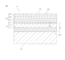
- the optical film F may include the pressure-sensitive adhesive layer 50 arranged on the other side of the transparent base material 10 in the thickness direction D.
- the pressure-sensitive adhesive layer 50 is a layer formed from a pressure-sensitive adhesive composition and has light transmittance.
- the tacky composition contains at least a base polymer that develops tackiness in the pressure-sensitive adhesive layer 50.
- the base polymer include acrylic polymers, rubber-based polymers, silicone-based polymers, urethane-based polymers, polyester-based polymers, and polyamide-based polymers. From the viewpoint of achieving both the adhesive strength required for the pressure-sensitive adhesive layer 50 of the optical film F and high transparency, an acrylic polymer is preferably used as the base polymer.
- the thickness of the pressure-sensitive adhesive layer 50 is preferably 5 ⁇ m or more, more preferably 10 ⁇ m or more, and more preferably 15 ⁇ m or more from the viewpoint of realizing sufficient adhesive force to the adherend in the optical film F. From the viewpoint of ensuring transparency, the thickness of the pressure-sensitive adhesive layer 50 is preferably 300 ⁇ m or less, more preferably 200 ⁇ m or less, still more preferably 100 ⁇ m or less.
- the optical film F shown in FIG. 2 can be manufactured, for example, as follows. First, the adhesive composition is applied onto the release liner to form a coating film. Next, the coating film on the release liner is dried as needed. As a result, the pressure-sensitive adhesive layer 50 is formed on the release liner. Next, the exposed surface of the pressure-sensitive adhesive layer 50 is bonded to the other surface (lower surface in FIG. 1) of the transparent base material 10 of the optical film F shown in FIG. 1 in the thickness direction D. For example, in this way, the optical film F shown in FIG. 2 can be manufactured.
- the optical film F includes the pressure-sensitive adhesive layer 50, no separate adhesive is required when bonding to the adherend.
- the present invention will be specifically described below with reference to examples.
- the present invention is not limited to the examples.
- the specific numerical values such as the compounding amount (content), the physical property value, the parameter, etc. described below are the compounding amounts corresponding to them described in the above-mentioned "form for carrying out the invention” (forms for carrying out the invention). It can be replaced with the upper limit (numerical value defined as “less than or equal to” or “less than”) or lower limit (numerical value defined as "greater than or equal to” or “greater than or equal to”) such as content), physical property value, and parameter.
- an antiglare hard coat layer was formed on one side of a triacetyl cellulose (TAC) film (thickness 80 ⁇ m) as a transparent resin film (hard coat layer forming step).
- TAC triacetyl cellulose
- the main components are Pentaeristol triacrylate, manufactured by Osaka Organic Chemical Industry Co., Ltd.) 50 parts by mass and polymethylmethacrylate particles as antiglare fine particles (trade name "Techpolymer”, average particle diameter 3 ⁇ m, refractive index 1.525, Sekisui Chemicals) (Manufactured by Kogyo Co., Ltd.) 3 parts by mass and silicone particles as antiglare fine particles (trade name "Tospearl 130", average particle diameter 3 ⁇ m, refractive index 1.
- a leveling agent (trade name "LE303", manufactured by Kyoeisha Chemical Co., Ltd.) and a mixed solvent of toluene, ethyl acetate and cyclopentanone (mass ratio 35:41:24) were mixed.
- a composition (crocodile) having a solid content concentration of 55% by mass was prepared.
- An ultrasonic disperser was used for mixing.
- the composition was applied to one side of the TAC film to form a coating film.
- this coating film was cured by irradiation with ultraviolet rays and then dried by heating.
- a high-pressure mercury lamp was used as a light source, ultraviolet rays having a wavelength of 365 nm were used, and the integrated irradiation light amount was set to 300 mJ / cm 2 .
- the heating temperature was 80 ° C., and the heating time was 60 seconds.
- an antiglare hard coat layer (first HC layer) having a thickness of 8 ⁇ m was formed on the TAC film.
- the surface of the HC layer of the TAC film with the HC layer was plasma-treated in a vacuum atmosphere of 1.0 Pa by a roll-to-roll type plasma processing device.
- argon gas was used as the inert gas, and the discharge power was set to 2400 W.
- an adhesion layer and an antireflection layer were sequentially formed on the HC layer of the TAC film with the HC layer after the plasma treatment (sputter film formation step).
- a roll-to-roll sputter film forming apparatus is used to add a 3.5 nm-thick SiOx layer (x ⁇ 2) as an adhesion layer on the HC layer of the TAC film with an HC layer after plasma treatment.
- Nb 2 O 5 layer with a thickness of 12 nm as the first high refractive index layer SiO 2 layer with a thickness of 28 nm as the first low refractive index layer, and Nb 2 with a thickness of 100 nm as the second high refractive index layer.
- a SiO 2 layer having a thickness of 85nm as a second low-refractive index layer are sequentially formed.
- a Si target is used, an argon gas as an inert gas and 3 parts by volume of oxygen gas as a reactive gas with respect to 100 parts by volume of the argon gas are used, and the discharge voltage is set to 520 V.
- the pressure in the film chamber (deposition pressure) was 0.27 Pa, and the SiOx layer (x ⁇ 2) was formed by MFAC sputtering.
- an Nb target is used, 100 parts by volume of argon gas and 5 parts by volume of oxygen gas are used, the discharge voltage is 415 V, the film formation pressure is 0.42 Pa, and Nb is formed by MFAC sputtering. the 2 O 5 layer was formed.
- a Si target is used, 100 parts by volume of argon gas and 30 parts by volume of oxygen gas are used, the discharge voltage is 350 V, the film formation pressure is 0.3 Pa, and SiO is used by MFAC sputtering. Two layers were formed.
- an Nb target is used, 100 parts by volume of argon gas and 13 parts by volume of oxygen gas are used, the discharge voltage is 460 V, the film formation pressure is 0.5 Pa, and Nb is Nb by MFAC sputtering. the 2 O 5 layer was formed.
- a Si target is used, 100 parts by volume of argon gas and 30 parts by volume of oxygen gas are used, the discharge voltage is 340 V, the film formation pressure is 0.25 Pa, and SiO is used by MFAC sputtering. Two layers were formed.
- the antireflection layer (first high refractive index layer, first low refractive index layer, second high refractive index layer, second low) is placed on the HC layer of the TAC film with the HC layer via the adhesion layer.
- the refractive index layer was laminated and formed.
- an antifouling layer was formed on the formed antireflection layer (antifouling layer forming step). Specifically, an antifouling layer having a thickness of 7 nm was formed on the antireflection layer by a vacuum vapor deposition method using an alkoxysilane compound containing a perfluoropolyether group as a vapor deposition source.
- the vapor deposition source is a solid content obtained by drying "Optur UD509" manufactured by Daikin Industries, Ltd. (perfluoropolyether group-containing alkoxysilane compound represented by the above general formula (2), solid content concentration 20% by mass). be.
- the heating temperature of the vapor deposition source in the vacuum vapor deposition method was 260 ° C.
- the optical film of Example 1 was produced.
- the optical film of Example 1 is provided with a transparent base material (resin film, hard coat layer), an adhesion layer, an antireflection layer, and an antifouling layer in this order toward one side in the thickness direction.
- Example 2 Example 1 except that the solid content obtained by drying "Optool UD120" (alkoxysilane compound containing a perfluoropolyether group) manufactured by Daikin Industries, Ltd. was used as the vapor deposition source in the antifouling layer forming step.
- the optical film of Example 2 was produced in the same manner as the optical film of Example 2.
- an antiglare hard coat layer was formed on one side of a triacetyl cellulose (TAC) film (thickness 80 ⁇ m) as a transparent resin film (hard coat layer forming step).
- TAC triacetyl cellulose
- an organosilica sol (trade name "MEK-") containing 100 parts by mass of an ultraviolet curable acrylic monomer (trade name "GRANDIC PC-1070", manufactured by DIC) and nanosilica particles as antiglare fine particles.
- the average primary particle size of the nanosilica particles is 50 nm
- the solid content concentration is 30% by mass, manufactured by Nissan Chemical Co., Ltd.) 1.5 parts by mass of synthetic smectite, which is an organic clay, manufactured by Corp Chemical Co., Ltd., 3 parts by mass of a photopolymerization initiator (trade name "OMNIRAD907", manufactured by BASF), and a leveling agent (trade name "LE303", Kyoeisha Chemical Co., Ltd.)
- a composition (crocodile) having a solid content concentration of 55% by mass was prepared by mixing with 0.15 parts by mass. An ultrasonic disperser was used for mixing. Next, the composition was applied to one side of the TAC film to form a coating film.
- this coating film was cured by irradiation with ultraviolet rays and then dried by heating.
- a high-pressure mercury lamp was used as a light source, ultraviolet rays having a wavelength of 365 nm were used, and the integrated irradiation light amount was set to 200 mJ / cm 2 .
- the heating time was 80 ° C., and the heating temperature was 3 minutes.
- an antiglare hard coat layer (second HC layer) having a thickness of 6 ⁇ m was formed on the TAC film.
- the surface of the HC layer of the TAC film with the HC layer was plasma-treated in a vacuum atmosphere of 1.0 Pa by a roll-to-roll type plasma processing device.
- argon gas was used as the inert gas, and the discharge power was set to 150 W.
- an adhesion layer and an antireflection layer were sequentially formed on the HC layer of the TAC film with the HC layer after the plasma treatment (sputter film formation step).
- a roll-to-roll sputter film forming apparatus is used to form an indium tin oxide (ITO) layer having a thickness of 1.5 nm as an adhesion layer on the HC layer of the TAC film with an HC layer after plasma treatment.
- ITO indium tin oxide
- Nb 2 O 5 layer with a thickness of 12 nm as the first high refractive index layer SiO 2 layer with a thickness of 28 nm as the first low refractive index layer
- Nb with a thickness of 100 nm as the second high refractive index layer.
- a SiO 2 layer having a thickness of 85nm as a second low-refractive index layer are sequentially formed.
- an ITO target is used, an argon gas as an inert gas and 10 parts by volume of oxygen gas as a reactive gas with respect to 100 parts by volume of the argon gas are used, and the discharge voltage is set to 400 V.
- the pressure in the film chamber (deposition pressure) was 0.2 Pa, and the ITO layer was formed by MFAC sputtering.
- the conditions for forming the first high refractive index layer, the first low refractive index layer, the second high refractive index layer, and the second low refractive index layer in the present embodiment are the first high refractive index layer and the first in the first embodiment.
- the conditions for forming the low refractive index layer, the second high refractive index layer, and the second low refractive index layer are the same as described above.
- an antifouling layer was formed on the formed antireflection layer (antifouling layer forming step). Specifically, it is the same as the antifouling layer forming step in Example 1 (as a vapor deposition source, a solid content obtained by drying "Optur UD509" manufactured by Daikin Industries, Ltd. was used).
- the optical film of Example 3 was produced.
- the optical film of Example 3 is provided with a transparent base material (resin film, hard coat layer), an adhesion layer, an antireflection layer, and an antifouling layer in this order toward one side in the thickness direction.
- Example 4 Example 3 except that the solid content obtained by drying "Optool UD120" (alkoxysilane compound containing a perfluoropolyether group) manufactured by Daikin Industries, Ltd. was used as the vapor deposition source in the antifouling layer forming step.
- the optical film of Example 4 was produced in the same manner as the optical film of Example 4.
- Example 5 This was carried out except that the solid content obtained by drying "KY-1901" (alkoxysilane compound containing a perfluoropolyether group) manufactured by Shin-Etsu Chemical Co., Ltd. was used as the vapor deposition source in the antifouling layer forming step.
- the optical film of Example 5 was produced in the same manner as the optical film of Example 3.
- Example 6 The optical film of Example 6 was produced in the same manner as the optical film of Example 3 except for the hard coat layer forming step and the antifouling layer forming step.
- the acrylic monomer composition containing nanosilica particles (trade name “NC035”, the average primary particle diameter of the nanosilica particles is 40 nm, the solid content concentration is 50% by mass, and the nanosilica in the solid content.
- the ratio of particles is 60% by mass, 67 parts by mass of Arakawa Chemical Industry Co., Ltd., and 33 parts by mass of ultraviolet curable polyfunctional acrylate (trade name "Binder A”, solid content concentration 100% by mass, manufactured by Arakawa Chemical Industry Co., Ltd.).
- polymethylmethacrylate particles as antiglare fine particles (trade name "Techpolymer”, average particle diameter 3 ⁇ m, refractive index 1.525, manufactured by Sekisui Kasei Kogyo Co., Ltd.), and silicone as antiglare fine particles.
- Particles (trade name "Tospearl 130", average particle diameter 3 ⁇ m, refractive index 1.42, manufactured by Momentive Performance Materials Japan) 1.5 parts by mass and thixotropy-imparting agent (trade name "Lucentite SAN", 1.5 parts by mass of synthetic smectite, which is an organic clay, manufactured by Corp Chemical Co., Ltd., 3 parts by mass of a photopolymerization initiator (trade name "OMNIRAD907", manufactured by BASF), and a leveling agent (trade name "LE303", Kyoeisha Chemical Co., Ltd.)
- a composition (crocodile) having a solid content concentration of 45% by mass was prepared by mixing 0.15 parts by mass and toluene.
- An ultrasonic disperser was used for mixing.
- the composition was applied to one side of the TAC film to form a coating film.
- this coating film was cured by irradiation with ultraviolet rays and then dried by heating.
- a high-pressure mercury lamp was used as a light source, ultraviolet rays having a wavelength of 365 nm were used, and the integrated irradiation light amount was set to 200 mJ / cm 2 .
- the heating time was 60 ° C., and the heating temperature was 60 seconds.
- an antiglare hard coat layer (third HC layer) having a thickness of 7 ⁇ m was formed on the TAC film.
- Example 6 a solid content obtained by drying "Optur UD120" (alkoxysilane compound containing a perfluoropolyether group) manufactured by Daikin Industries, Ltd. was used as a vapor deposition source.
- Example 7 This was carried out except that the solid content obtained by drying "KY-1901" (alkoxysilane compound containing a perfluoropolyether group) manufactured by Shin-Etsu Chemical Co., Ltd. was used as the vapor deposition source in the antifouling layer forming step.
- the optical film of Example 7 was produced in the same manner as the optical film of Example 6.
- Example 8 The optical film of Example 8 was produced in the same manner as the optical film of Example 3 except for the hard coat layer forming step and the antifouling layer forming step.
- the acrylic monomer composition containing nanosilica particles (trade name “NC035HS”, the average primary particle diameter of the nanosilica particles is 40 nm, the solid content concentration is 50% by mass, and the nanosilica in the solid content. Particle ratio is 60% by mass, manufactured by Arakawa Chemical Industry Co., Ltd.
- UV curable polyfunctional urethane acrylate (trade name "Beamset 580", solid content concentration 70% by mass, manufactured by Arakawa Chemical Industry Co., Ltd.) 17 4 parts by mass and 4 parts by mass of polymethylmethacrylate particles (trade name "Techpolymer”, average particle diameter 3 ⁇ m, refractive index 1.495, manufactured by Sekisui Kasei Kogyo Co., Ltd.) as antiglare fine particles, and as antiglare fine particles Silicone particles (trade name "Tospearl 130", average particle diameter 3 ⁇ m, refractive index 1.42, manufactured by Momentive Performance Materials Japan Co., Ltd.) 0.1 part by mass and thixotropy-imparting agent (trade name "Lucentite SAN”) , 2.0 parts by mass of synthetic smectite, which is an organic clay, manufactured by Coop Chemical Co., Ltd., 3 parts by mass of a photopolymerization initiator (trade name "OMNIRAD907", manufactured by
- An ultrasonic disperser was used for mixing.
- the composition was applied to one side of the TAC film to form a coating film.
- this coating film was cured by irradiation with ultraviolet rays and then dried by heating.
- a high-pressure mercury lamp was used as a light source, ultraviolet rays having a wavelength of 365 nm were used, and the integrated irradiation light amount was set to 200 mJ / cm 2 .
- the heating time was 60 ° C., and the heating temperature was 60 seconds.
- an antiglare hard coat layer fourth HC layer having a thickness of 8 ⁇ m was formed on the TAC film.
- Example 8 a solid content obtained by drying "KY-1903-1" (alkoxysilane compound containing a perfluoropolyether group) manufactured by Shin-Etsu Chemical Co., Ltd. is used as a vapor deposition source. board.
- Comparative Example 1 The optical film of Comparative Example 1 was produced in the same manner as the optical film of Example 1 except for the antifouling layer forming step.
- ⁇ Water contact angle> The water contact angle on the surface of the antifouling layer was examined for each of the optical films of Examples 1 to 8 and Comparative Example 1. First, water droplets were formed on the surface of the antifouling layer of the optical film by dropping about 1 ⁇ L of pure water. Next, the angle formed by the surface of the water droplet on the surface of the antifouling layer and the surface of the antifouling layer was measured. A contact angle meter (trade name "DMo-501", manufactured by Kyowa Interface Science Co., Ltd.) was used for the measurement. The measurement results are shown in Table 1.
- ⁇ Surface roughness Ra> The surface roughness Ra of the antifouling layer was examined for each of the optical films of Examples 1 to 8 and Comparative Example 1. Specifically, the surface of the antifouling layer of each optical film is observed with an atomic force microscope (trade name "SPI3800", manufactured by Seiko Instruments, Inc.), and the surface roughness Ra (arithmetic mean roughness) is observed in a 1 ⁇ m square observation image. I asked for it. The results are shown in Table 1.
- the transparent base material side of the sample film (50 mm ⁇ 50 mm) cut out from the optical film was attached to a black acrylic plate via an adhesive.
- total reflection measurement was performed on the sample bonded to the black acrylic plate using a spectrophotometer (trade name "U-4100", manufactured by Hitachi High-Technologies Corporation). Based on the spectral reflectance at a wavelength of 380 to 780 nm obtained by this measurement and the relative spectral distribution of the CIE standard Illuminant D65, the three stimuli of the object color due to reflection in the XYZ color system defined by JIS Z8701. The value Y was calculated and the total reflection Y value was obtained.
- the scattered light was removed by using a spectrophotometer (trade name "U-4100") and the jig attached to the U-4100. Specular reflection measurement was performed under the condition of an incident angle of 5 °. Based on the spectral reflectance at a wavelength of 380 to 780 nm obtained by this measurement and the relative spectral distribution of the CIE standard Illuminant D65, the three stimuli of the object color due to reflection in the XYZ color system defined by JIS Z8701. The value Y was calculated and the normal reflection Y value was obtained.
- the ratio of (Y 2 / Y 1 ) is shown in Table 1.
- ⁇ Surface haze> The surface haze of each of the optical films of Examples 1 to 8 and Comparative Example 1 was examined. Specifically, first, the sample film cut out from the optical film was subjected to haze measurement based on JIS K 7136 (2000) using "Haze Meter HM150" manufactured by Murakami Color Technology Research Institute (this). Measures the total haze value of the sample film). Next, in a state where the cycloolefin polymer film was attached to the surface of the sample film on the antifouling layer side via an adhesive to eliminate the surface haze of the sample film, the "haze meter HM150" manufactured by Murakami Color Technology Research Institute was used.
- the antifouling property of the antifouling layer was examined for each of the optical films of Examples 1 to 8 and Comparative Example 1. Specifically, first, the surface of the antifouling layer of the optical film was touched with a finger to attach a fingerprint. Next, the fingerprint was wiped with a cotton cloth (work of sweeping the waste in one direction while bringing the waste into contact with the area including the fingerprint adhesion portion on the surface of the antifouling layer) three times. Then, regarding the antifouling property of the antifouling layer, the case where the fingerprint is wiped off by three wiping operations is evaluated as "good", and the case where the fingerprint is not wiped off even after three wiping operations (that is, a part of the fingerprint). (If remains) was evaluated as "defective”. The results are shown in Table 1.
- the optical film with an antifouling layer of the present invention can be applied to, for example, an antireflection film with an antifouling layer, a transparent conductive film with an antifouling layer, and an electromagnetic wave shielding film with an antifouling layer.
- Optical film (optical film with antifouling layer) 10 Transparent base material 11 Resin film 12 Hard coat layer 20 Optical functional layer 21 First high refractive index layer 22 First low refractive index layer 23 Second high refractive index layer 24 Second low refractive index layer 30 Antifouling layer 31 Outer surface 40 Adhesive layer 50 Adhesive layer
Landscapes
- Physics & Mathematics (AREA)
- Chemical & Material Sciences (AREA)
- Engineering & Computer Science (AREA)
- Optics & Photonics (AREA)
- General Physics & Mathematics (AREA)
- Mechanical Engineering (AREA)
- Chemical Kinetics & Catalysis (AREA)
- Inorganic Chemistry (AREA)
- Organic Chemistry (AREA)
- Metallurgy (AREA)
- Materials Engineering (AREA)
- Health & Medical Sciences (AREA)
- Manufacturing & Machinery (AREA)
- Ophthalmology & Optometry (AREA)
- Laminated Bodies (AREA)
- Surface Treatment Of Optical Elements (AREA)
Priority Applications (3)
| Application Number | Priority Date | Filing Date | Title |
|---|---|---|---|
| JP2022536371A JP7389259B2 (ja) | 2020-07-13 | 2021-07-13 | 防汚層付き光学フィルム |
| KR1020227045057A KR102666261B1 (ko) | 2020-07-13 | 2021-07-13 | 방오층이 형성된 광학 필름 |
| CN202180049523.3A CN115803194A (zh) | 2020-07-13 | 2021-07-13 | 带防污层的光学薄膜 |
Applications Claiming Priority (4)
| Application Number | Priority Date | Filing Date | Title |
|---|---|---|---|
| JP2020120131 | 2020-07-13 | ||
| JP2020-120131 | 2020-07-13 | ||
| JP2020-146144 | 2020-08-31 | ||
| JP2020146144 | 2020-08-31 |
Publications (1)
| Publication Number | Publication Date |
|---|---|
| WO2022014567A1 true WO2022014567A1 (ja) | 2022-01-20 |
Family
ID=79555556
Family Applications (1)
| Application Number | Title | Priority Date | Filing Date |
|---|---|---|---|
| PCT/JP2021/026245 Ceased WO2022014567A1 (ja) | 2020-07-13 | 2021-07-13 | 防汚層付き光学フィルム |
Country Status (5)
| Country | Link |
|---|---|
| JP (1) | JP7389259B2 (enExample) |
| KR (1) | KR102666261B1 (enExample) |
| CN (1) | CN115803194A (enExample) |
| TW (1) | TWI838633B (enExample) |
| WO (1) | WO2022014567A1 (enExample) |
Cited By (3)
| Publication number | Priority date | Publication date | Assignee | Title |
|---|---|---|---|---|
| WO2025013861A1 (ja) * | 2023-07-11 | 2025-01-16 | 日東電工株式会社 | 反射防止フィルム |
| JPWO2025013860A1 (enExample) * | 2023-07-11 | 2025-01-16 | ||
| WO2025013857A1 (ja) * | 2023-07-11 | 2025-01-16 | 日東電工株式会社 | 積層フィルム |
Families Citing this family (1)
| Publication number | Priority date | Publication date | Assignee | Title |
|---|---|---|---|---|
| KR102856327B1 (ko) * | 2024-01-08 | 2025-09-05 | (주)인터코닉스 | 폴더블이 가능한 비반사 복합구조의 디스플레이 보호필름 |
Citations (7)
| Publication number | Priority date | Publication date | Assignee | Title |
|---|---|---|---|---|
| JP2003276109A (ja) * | 2002-03-26 | 2003-09-30 | Dainippon Printing Co Ltd | 透明積層フィルムの製造方法及び透明積層フィルム及び反射防止フィルム |
| WO2005097483A1 (ja) * | 2004-03-31 | 2005-10-20 | Dai Nippon Printing Co., Ltd. | 反射防止積層体 |
| JP2010156982A (ja) * | 2004-02-16 | 2010-07-15 | Fujifilm Corp | 反射防止フィルム、それを用いた偏光板、及びそれらを用いた画像表示装置 |
| JP2017161893A (ja) * | 2016-03-03 | 2017-09-14 | 日東電工株式会社 | 光学積層体 |
| WO2018207811A1 (ja) * | 2017-05-12 | 2018-11-15 | Agc株式会社 | 防汚性物品および防汚性物品の製造方法 |
| JP2020052221A (ja) * | 2018-09-26 | 2020-04-02 | 日東電工株式会社 | 保護フィルム付き光学フィルム |
| WO2021106797A1 (ja) * | 2019-11-25 | 2021-06-03 | 日東電工株式会社 | 反射防止フィルムおよび画像表示装置 |
Family Cites Families (15)
| Publication number | Priority date | Publication date | Assignee | Title |
|---|---|---|---|---|
| JP3836214B2 (ja) * | 1997-05-12 | 2006-10-25 | 凸版印刷株式会社 | 反射防止材及び光学部材 |
| JP2001188102A (ja) * | 1999-12-27 | 2001-07-10 | Toppan Printing Co Ltd | 反射防止フィルム |
| JP5102958B2 (ja) * | 2005-12-15 | 2012-12-19 | 富士フイルム株式会社 | 反射防止フィルムの製造方法 |
| JP2007194109A (ja) | 2006-01-20 | 2007-08-02 | Toppan Printing Co Ltd | 導電性積層体、光学機能性フィルタおよび光学表示装置 |
| JP5252811B2 (ja) * | 2006-05-16 | 2013-07-31 | 日東電工株式会社 | 防眩性ハードコートフィルム、偏光板および画像表示装置 |
| EP2915833B1 (en) * | 2012-11-05 | 2018-06-06 | Daikin Industries, Ltd. | Silane compound containing perfluoro(poly)ether group |
| CN112442206B (zh) | 2015-05-27 | 2023-08-18 | 迪睿合株式会社 | 层叠薄膜 |
| CN107428786B (zh) * | 2015-07-31 | 2019-04-30 | 大金工业株式会社 | 含有全氟(聚)醚基的硅烷化合物 |
| JP6774383B2 (ja) | 2016-06-17 | 2020-10-21 | 日東電工株式会社 | 反射防止フィルムおよびその製造方法、ならびに反射防止層付き偏光板 |
| US20200002551A1 (en) * | 2017-02-03 | 2020-01-02 | Daikin Industries, Ltd. | Perfluoro(poly)ether group-containing compound, and surface treatment agent and article including same |
| KR102569079B1 (ko) * | 2017-04-20 | 2023-08-22 | 신에쓰 가가꾸 고교 가부시끼가이샤 | 반사방지 부재 및 그 제조 방법 |
| CN110831757A (zh) * | 2017-08-16 | 2020-02-21 | 日产自动车株式会社 | 防污结构体 |
| JP6999370B2 (ja) * | 2017-11-06 | 2022-01-18 | 日東電工株式会社 | 反射防止層付偏光板およびその製造方法 |
| WO2019208786A1 (ja) | 2018-04-27 | 2019-10-31 | 大日本印刷株式会社 | 光学フィルム、偏光板、および画像表示装置 |
| JP2020060657A (ja) * | 2018-10-09 | 2020-04-16 | 日東電工株式会社 | 反射防止ガラス |
-
2021
- 2021-07-13 CN CN202180049523.3A patent/CN115803194A/zh active Pending
- 2021-07-13 KR KR1020227045057A patent/KR102666261B1/ko active Active
- 2021-07-13 JP JP2022536371A patent/JP7389259B2/ja active Active
- 2021-07-13 TW TW110125719A patent/TWI838633B/zh active
- 2021-07-13 WO PCT/JP2021/026245 patent/WO2022014567A1/ja not_active Ceased
Patent Citations (7)
| Publication number | Priority date | Publication date | Assignee | Title |
|---|---|---|---|---|
| JP2003276109A (ja) * | 2002-03-26 | 2003-09-30 | Dainippon Printing Co Ltd | 透明積層フィルムの製造方法及び透明積層フィルム及び反射防止フィルム |
| JP2010156982A (ja) * | 2004-02-16 | 2010-07-15 | Fujifilm Corp | 反射防止フィルム、それを用いた偏光板、及びそれらを用いた画像表示装置 |
| WO2005097483A1 (ja) * | 2004-03-31 | 2005-10-20 | Dai Nippon Printing Co., Ltd. | 反射防止積層体 |
| JP2017161893A (ja) * | 2016-03-03 | 2017-09-14 | 日東電工株式会社 | 光学積層体 |
| WO2018207811A1 (ja) * | 2017-05-12 | 2018-11-15 | Agc株式会社 | 防汚性物品および防汚性物品の製造方法 |
| JP2020052221A (ja) * | 2018-09-26 | 2020-04-02 | 日東電工株式会社 | 保護フィルム付き光学フィルム |
| WO2021106797A1 (ja) * | 2019-11-25 | 2021-06-03 | 日東電工株式会社 | 反射防止フィルムおよび画像表示装置 |
Cited By (7)
| Publication number | Priority date | Publication date | Assignee | Title |
|---|---|---|---|---|
| WO2025013861A1 (ja) * | 2023-07-11 | 2025-01-16 | 日東電工株式会社 | 反射防止フィルム |
| JPWO2025013860A1 (enExample) * | 2023-07-11 | 2025-01-16 | ||
| JPWO2025013861A1 (enExample) * | 2023-07-11 | 2025-01-16 | ||
| WO2025013860A1 (ja) * | 2023-07-11 | 2025-01-16 | 日東電工株式会社 | 反射防止フィルム |
| WO2025013857A1 (ja) * | 2023-07-11 | 2025-01-16 | 日東電工株式会社 | 積層フィルム |
| JP2025011543A (ja) * | 2023-07-11 | 2025-01-24 | 日東電工株式会社 | 積層フィルム |
| JP7730864B2 (ja) | 2023-07-11 | 2025-08-28 | 日東電工株式会社 | 積層フィルム |
Also Published As
| Publication number | Publication date |
|---|---|
| CN115803194A (zh) | 2023-03-14 |
| KR20230037013A (ko) | 2023-03-15 |
| TW202234092A (zh) | 2022-09-01 |
| JP7389259B2 (ja) | 2023-11-29 |
| TWI838633B (zh) | 2024-04-11 |
| KR102666261B1 (ko) | 2024-05-20 |
| JPWO2022014567A1 (enExample) | 2022-01-20 |
Similar Documents
| Publication | Publication Date | Title |
|---|---|---|
| JP7389259B2 (ja) | 防汚層付き光学フィルム | |
| KR102518012B1 (ko) | 방오층이 형성된 광학 필름 | |
| JP7130893B2 (ja) | 防汚層付き光学フィルム | |
| JP2022079332A (ja) | 防汚層付き光学フィルム | |
| JP7219849B2 (ja) | 防汚層付き光学フィルム | |
| CN115803187B (zh) | 带防污层的光学薄膜 | |
| KR102548030B1 (ko) | 방오층이 형성된 광학 필름 | |
| WO2022014570A1 (ja) | 防汚層付き光学フィルム | |
| JP7538299B1 (ja) | 反射防止フィルム及び画像表示装置 | |
| JP2024098719A (ja) | 反射防止フィルム及び画像表示装置 | |
| JP2025168854A (ja) | 反射防止フィルム及びその製造方法 | |
| JP2024098718A (ja) | 反射防止フィルム及び画像表示装置 | |
| JP2024072451A (ja) | 光学フィルム | |
| WO2022137832A1 (ja) | 光学フィルム |
Legal Events
| Date | Code | Title | Description |
|---|---|---|---|
| 121 | Ep: the epo has been informed by wipo that ep was designated in this application |
Ref document number: 21841208 Country of ref document: EP Kind code of ref document: A1 |
|
| ENP | Entry into the national phase |
Ref document number: 2022536371 Country of ref document: JP Kind code of ref document: A |
|
| NENP | Non-entry into the national phase |
Ref country code: DE |
|
| 122 | Ep: pct application non-entry in european phase |
Ref document number: 21841208 Country of ref document: EP Kind code of ref document: A1 |