WO2022014567A1 - 防汚層付き光学フィルム - Google Patents
防汚層付き光学フィルム Download PDFInfo
- Publication number
- WO2022014567A1 WO2022014567A1 PCT/JP2021/026245 JP2021026245W WO2022014567A1 WO 2022014567 A1 WO2022014567 A1 WO 2022014567A1 JP 2021026245 W JP2021026245 W JP 2021026245W WO 2022014567 A1 WO2022014567 A1 WO 2022014567A1
- Authority
- WO
- WIPO (PCT)
- Prior art keywords
- layer
- optical film
- refractive index
- film
- antifouling
- Prior art date
Links
Images
Classifications
-
- B—PERFORMING OPERATIONS; TRANSPORTING
- B32—LAYERED PRODUCTS
- B32B—LAYERED PRODUCTS, i.e. PRODUCTS BUILT-UP OF STRATA OF FLAT OR NON-FLAT, e.g. CELLULAR OR HONEYCOMB, FORM
- B32B27/00—Layered products comprising a layer of synthetic resin
-
- B—PERFORMING OPERATIONS; TRANSPORTING
- B32—LAYERED PRODUCTS
- B32B—LAYERED PRODUCTS, i.e. PRODUCTS BUILT-UP OF STRATA OF FLAT OR NON-FLAT, e.g. CELLULAR OR HONEYCOMB, FORM
- B32B7/00—Layered products characterised by the relation between layers; Layered products characterised by the relative orientation of features between layers, or by the relative values of a measurable parameter between layers, i.e. products comprising layers having different physical, chemical or physicochemical properties; Layered products characterised by the interconnection of layers
- B32B7/02—Physical, chemical or physicochemical properties
- B32B7/023—Optical properties
-
- C—CHEMISTRY; METALLURGY
- C23—COATING METALLIC MATERIAL; COATING MATERIAL WITH METALLIC MATERIAL; CHEMICAL SURFACE TREATMENT; DIFFUSION TREATMENT OF METALLIC MATERIAL; COATING BY VACUUM EVAPORATION, BY SPUTTERING, BY ION IMPLANTATION OR BY CHEMICAL VAPOUR DEPOSITION, IN GENERAL; INHIBITING CORROSION OF METALLIC MATERIAL OR INCRUSTATION IN GENERAL
- C23C—COATING METALLIC MATERIAL; COATING MATERIAL WITH METALLIC MATERIAL; SURFACE TREATMENT OF METALLIC MATERIAL BY DIFFUSION INTO THE SURFACE, BY CHEMICAL CONVERSION OR SUBSTITUTION; COATING BY VACUUM EVAPORATION, BY SPUTTERING, BY ION IMPLANTATION OR BY CHEMICAL VAPOUR DEPOSITION, IN GENERAL
- C23C14/00—Coating by vacuum evaporation, by sputtering or by ion implantation of the coating forming material
- C23C14/06—Coating by vacuum evaporation, by sputtering or by ion implantation of the coating forming material characterised by the coating material
-
- G—PHYSICS
- G02—OPTICS
- G02B—OPTICAL ELEMENTS, SYSTEMS OR APPARATUS
- G02B1/00—Optical elements characterised by the material of which they are made; Optical coatings for optical elements
- G02B1/10—Optical coatings produced by application to, or surface treatment of, optical elements
- G02B1/11—Anti-reflection coatings
- G02B1/113—Anti-reflection coatings using inorganic layer materials only
-
- G—PHYSICS
- G02—OPTICS
- G02B—OPTICAL ELEMENTS, SYSTEMS OR APPARATUS
- G02B1/00—Optical elements characterised by the material of which they are made; Optical coatings for optical elements
- G02B1/10—Optical coatings produced by application to, or surface treatment of, optical elements
- G02B1/18—Coatings for keeping optical surfaces clean, e.g. hydrophobic or photo-catalytic films
Definitions
- the present invention relates to an optical film with an antifouling layer.
- a transparent optical film provided with a layer having a predetermined optical function (optical functional layer) is provided.
- the optical film include an antireflection film, a transparent conductive film, and an electromagnetic wave shielding film.
- the optical film includes, for example, a transparent base material, an optical functional layer arranged on one side thereof, and an adhesive layer arranged on the other side of the transparent base material. A technique relating to such an optical film is described in, for example, Patent Document 1 below.
- the optical film in which the optical functional layer is arranged as the outermost layer, contaminants such as hand grease are likely to adhere to the optical functional layer, and the adhered contaminants are difficult to be removed from the optical functional layer. Adhesion of contaminants on the optical film is not preferable from the viewpoint of ensuring the transparency of the optical film. Therefore, for example, the optical film is provided with an antifouling layer as the outermost layer. In such an optical film with an antifouling layer, high antifouling property is required in the antifouling layer.
- the present invention provides an optical film with an antifouling layer suitable for achieving high antifouling properties in the antifouling layer.
- the present invention [1] includes a transparent base material, an optical functional layer, and an antifouling layer in this order, and the outer surface of the antifouling layer on the opposite side of the optical functional layer has a water contact angle of 110 ° or more. Includes an optical film with an antifouling layer.
- the present invention [2] includes the optical film with an antifouling layer according to the above [1], wherein the outer surface has a surface roughness Ra of more than 2 nm.
- the present invention [3] includes the optical film with an antifouling layer according to the above [1] or [2], wherein the optical functional layer is an antireflection layer.
- the antireflection layer according to the above [3], wherein the antireflection layer alternately includes a high refractive index layer having a relatively large refractive index and a low refractive index layer having a relatively small refractive index. includes an optical film with a foul layer.
- the present invention [5] includes the optical film with an antifouling layer according to any one of the above [1] to [4], wherein the transparent substrate has a hard coat layer on the optical functional layer side.
- the present invention [6] includes the optical film with an antifouling layer according to the above [5], wherein the hard coat layer contains metal oxide fine particles.
- the present invention [7] includes the optical film with an antifouling layer according to the above [6], wherein the metal oxide fine particles are nanosilica particles.
- the protection according to any one of the above [5] to [7], wherein the surface of the hard coat layer on the optical functional layer side has a surface roughness Ra of 0.5 nm or more and 20 nm or less. includes an optical film with a dirty layer.
- the optical film with an antifouling layer of the present invention realizes high antifouling property in the antifouling layer because the outer surface of the antifouling layer opposite to the optical functional layer has a water contact angle of 110 ° or more. Suitable for.
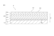
- the optical film F as an embodiment of the optical film with an antifouling layer of the present invention comprises a transparent base material 10, an optical functional layer 20, and an antifouling layer 30 in a thickness direction D. Prepare in this order toward one side.
- the optical film F is preferably provided with the transparent base material 10, the adhesion layer 40, the optical functional layer 20, and the antifouling layer 30 in this order toward one side in the thickness direction D. Is composed of a transparent base material 10, an adhesion layer 40, an optical functional layer 20, and an antifouling layer 30.
- the optical film F has a shape that spreads in a direction (plane direction) orthogonal to the thickness direction D.
- the transparent base material 10 is provided with the resin film 11 and the hard coat layer 12 in this order toward one side in the thickness direction D.
- the resin film 11 is a transparent resin film having flexibility.
- the material of the resin film 11 include polyester resin, polyolefin resin, polystyrene resin, acrylic resin, polycarbonate resin, polyether sulfone resin, polysulfone resin, polyamide resin, polyimide resin, cellulose resin, norbornene resin, polyarylate resin, and Polyvinyl alcohol resin can be mentioned.
- the polyester resin include polyethylene terephthalate (PET), polybutylene terephthalate, and polyethylene naphthalate.
- the polyolefin resin include polyethylene, polypropylene, and cycloolefin polymers.
- the cellulose resin include triacetyl cellulose. These materials may be used alone or in combination of two or more. From the viewpoint of transparency and strength, cellulose resin is preferably used as the material of the resin film 11, and triacetyl cellulose is more preferably used.
- the surface of the resin film 11 on the hard coat layer 12 side may be surface-modified.
- Examples of the surface modification treatment include corona treatment, plasma treatment, ozone treatment, primer treatment, glow treatment, and coupling agent treatment.
- the thickness of the resin film 11 is preferably 5 ⁇ m or more, more preferably 10 ⁇ m or more, and further preferably 20 ⁇ m or more.
- the thickness of the resin film 11 is preferably 300 ⁇ m or less, more preferably 200 ⁇ m or less, from the viewpoint of handleability.
- the visible light transmittance of the resin film 11 is preferably 80% or more, more preferably 90% or more from the viewpoint of transparency.
- the visible light transmittance of the resin film 11 is, for example, 100% or less.
- the hard coat layer 12 is arranged on one side of the resin film 11 in the thickness direction D.
- the hard coat layer 12 is a layer for making it difficult for scratches to be formed on the exposed surface (upper surface in FIG. 1) of the optical film F.
- the hard coat layer 12 is a cured product of the curable resin composition.
- the curable resin contained in the curable resin composition include polyester resin, acrylic resin, urethane resin, acrylic urethane resin, amide resin, silicone resin, epoxy resin, and melamine resin. These curable resins may be used alone or in combination of two or more. From the viewpoint of ensuring high hardness of the hard coat layer 12, an acrylic resin and / or an acrylic urethane resin is preferably used as the curable resin.
- examples of the curable resin composition include an ultraviolet curable resin composition and a thermosetting resin composition.
- an ultraviolet curable resin composition is preferably used from the viewpoint of helping to improve the production efficiency of the optical film F because it can be cured without heating at a high temperature.
- the UV curable resin composition contains at least one selected from the group consisting of UV curable monomers, UV curable oligomers, and UV curable polymers. Examples of the ultraviolet curable resin composition include the composition for forming a hard coat layer described in JP-A-2016-179686.
- the hard coat layer 12 may be a hard coat layer (anti-glare hard coat layer) having anti-glare properties.
- the hard coat layer 12 as the anti-glare hard coat layer is a curing of a curable resin composition containing a curable resin (matrix resin) and fine particles (anti-glare fine particles) for exhibiting anti-glare properties. It is a thing.
- the antiglare fine particles include metal oxide fine particles and organic fine particles.
- Examples of the material of the metal oxide fine particles include silica, alumina, titania, zirconia, calcium oxide, tin oxide, indium oxide, kadomium oxide, and antimony oxide.
- Materials for organic microparticles include polymethylmethacrylate, silicone, polystyrene, polyurethane, acrylic-styrene copolymers, benzoguanamines, melamines, and polycarbonates. These fine particles may be used alone or in combination of two or more. From the viewpoint of exhibiting good antiglare properties in the hardcoat layer 12, at least one selected from the group consisting of nanosilica particles, polymethylmethacrylate particles, and silicone particles is preferably used as the antiglare fine particles. Be done.
- the average particle size of the fine particles is, for example, 10 ⁇ m or less, preferably 8 ⁇ m or less, and is, for example, 1 nm or more.
- the average particle size of the fine particles is, for example, 100 nm or less, preferably 70 nm or less, and for example, 1 nm or more.
- the average particle size of the fine particles is determined as a D50 value (cumulative 50% median diameter) based on, for example, the particle size distribution obtained by the particle size distribution measurement method in the laser scattering method.
- the refractive index of the matrix resin is, for example, 1.46 or more, preferably 1.49 or more, more preferably 1.50 or more, and further preferably 1.51 or more.
- the refractive index is, for example, 1.60 or less, preferably 1.59 or less, more preferably 1.58 or less, still more preferably 1.57 or less.
- the refractive index of the fine particles may be higher or lower than the above-mentioned refractive index of the matrix resin.
- the refractive index of the fine particles is, for example, 1.62 or less, preferably 1.60 or less, more preferably 1.59 or less, still more preferably 1.50. It is as follows.
- the refractive index of the fine particles is, for example, 1.40 or more, preferably 1.42 or more, and more preferably 1.44 or more.
- the content of the fine particles in the hard coat layer 12 is preferably 1 part by mass or more, and more preferably 3 parts by mass or more with respect to 100 parts by mass of the matrix resin.
- the content of the fine particles in the hard coat layer 12 is preferably 30 parts by mass or less, and more preferably 20 parts by mass or less with respect to 100 parts by mass of the matrix resin.
- the thickness of the hard coat layer 12 is preferably 0.5 ⁇ m or more, more preferably 1 ⁇ m or more, from the viewpoint of ensuring the hardness of the same layer.
- the thickness of the hard coat layer 12 is, for example, 10 ⁇ m or less.
- the surface of the hard coat layer 12 on the adhesion layer 40 side may be surface-modified.
- Examples of the surface modification treatment include plasma treatment, corona treatment, ozone treatment, primer treatment, glow treatment, and coupling agent treatment. From the viewpoint of ensuring a high adhesion between the hard coat layer 12 and the adhesion layer 40, the surface of the hard coat layer 12 on the adhesion layer 40 side is preferably glow-treated.
- the thickness of the transparent substrate 10 is preferably 5 ⁇ m or more, more preferably 10 ⁇ m or more, and further preferably 20 ⁇ m or more.
- the thickness of the transparent substrate 10 is preferably 300 ⁇ m or less, more preferably 200 ⁇ m or less, from the viewpoint of handleability.
- the visible light transmittance of the transparent base material 10 is preferably 80% or more, more preferably 90% or more from the viewpoint of transparency.
- the visible light transmittance of the transparent substrate 10 is, for example, 100% or less.
- the surface roughness Ra (arithmetic mean surface roughness) of the surface of the transparent substrate 10 on the optical functional layer 20 side (in this embodiment, the surface of the hard coat layer 12 on the optical functional layer 20 side) is preferably 0.5 nm. As mentioned above, it is more preferably 0.8 nm or more.
- the surface roughness Ra is preferably 20 nm or less, more preferably 15 nm or less.
- the surface roughness Ra is obtained from, for example, an observation image of 1 ⁇ m square by an AFM (atomic force microscope).
- the adhesion layer 40 is a layer for ensuring the adhesion between the transparent base material 10 and the optical functional layer 20.
- the adhesion layer 40 is arranged on one side of the transparent base material 10 (specifically, the hard coat layer 12 of the transparent base material 10 in the present embodiment) in the thickness direction D.
- Examples of the material of the adhesion layer 40 include metals such as silicon, nickel, chromium, aluminum, tin, gold, silver, platinum, zinc, titanium, tungsten, zirconium, and palladium, two or more alloys of these metals, and Examples thereof include oxides of these metals.
- silicon oxide (SiOx) or indium tin oxide (ITO) is preferably used as the material of the adhesion layer 40.
- SiOx having a smaller oxygen content than the stoichiometric composition is preferably used, and more preferably SiOx having x of 1.2 or more and 1.9 or less is used. ..
- the thickness of the adhesion layer 40 is, for example, 1 nm or more, and is, for example, 10 nm from the viewpoint of ensuring the adhesion between the transparent base material 10 and the optical functional layer 20 and the transparency of the adhesion layer 40. It is as follows.
- the optical functional layer 20 is arranged on one surface of the adhesion layer 40 in the thickness direction D.
- the optical functional layer 20 is an antireflection layer for suppressing the reflection intensity of external light. That is, the optical film F is an antireflection film in this embodiment.
- the optical functional layer 20 (antireflection layer) has a high refractive index layer having a relatively large refractive index and a low refractive index layer having a relatively small refractive index alternately in the thickness direction.
- the net reflected light intensity is attenuated by the interference action between the reflected light at the plurality of interfaces in the plurality of thin layers (high refractive index layer, low refractive index layer) contained therein.
- an interference effect for attenuating the reflected light intensity can be exhibited by adjusting the optical film thickness (product of the refractive index and the thickness) of each thin layer.
- the optical functional layer 20 as such an antireflection layer includes a first high refractive index layer 21, a first low refractive index layer 22, and a second high refractive index layer 23.
- the second low refractive index layer 24 is provided in this order toward one side in the thickness direction D.
- the first high-refractive index layer 21 and the second high-refractive index layer 23 are each made of a high-refractive index material having a refractive index of preferably 1.9 or more at a wavelength of 550 nm.
- high refractive index materials include, for example, niobium oxide (Nb 2 O 5 ), titanium oxide, zirconium oxide, tin-doped indium oxide (ITO), and antimony.
- Dope tin oxide (ATO) is mentioned, and niobium oxide is preferably used.
- the optical film thickness (product of refractive index and thickness) of the first high refractive index layer 21 is, for example, 20 nm or more, and is, for example, 55 nm or less.
- the optical film thickness of the second high-refractive index layer 23 is, for example, 60 nm or more, and for example, 330 nm or less.
- the first low refractive index layer 22 and the second low refractive index layer 24 are each made of a low refractive index material having a refractive index of preferably 1.6 or less at a wavelength of 550 nm.
- examples of the low refractive index material include silicon dioxide (SiO 2 ) and magnesium fluoride, and silicon dioxide is preferably used.
- silicon dioxide is preferably used as the material of the second low refractive index layer 24, silicon dioxide is preferably used from the viewpoint of ensuring the adhesion between the second low refractive index layer 24 and the antifouling layer 30.
- the optical film thickness of the first low refractive index layer 22 is, for example, 15 nm or more, and is, for example, 70 nm or less.
- the optical film thickness of the second low refractive index layer 24 is, for example, 100 nm or more, and is, for example, 160 nm or less.
- the thickness of the first high refractive index layer 21 is, for example, 1 nm or more, preferably 5 nm or more, and for example, 30 nm or less, preferably 20 nm or less.
- the thickness of the first low refractive index layer 22 is, for example, 10 nm or more, preferably 20 nm or more, and for example, 50 nm or less, preferably 30 nm or less.
- the thickness of the second high refractive index layer 23 is, for example, 50 nm or more, preferably 80 nm or more, and for example, 200 nm or less, preferably 150 nm or less.
- the thickness of the second low refractive index layer 24 is, for example, 60 nm or more, preferably 80 nm or more, and for example, 150 nm or less, preferably 100 nm or less.
- the antifouling layer 30 is a layer having an antifouling function in the optical film F, and is arranged on one surface of the optical functional layer 20 in the thickness direction D.
- the antifouling layer 30 has an outer surface 31 on one side in the thickness direction D.
- the antifouling function of the antifouling layer 30 includes a function of suppressing the adhesion of contaminants such as hand grease to the exposed surface of the film when the optical film F is used, and a function of facilitating the removal of the adhered contaminants.
- Examples of the material of the antifouling layer 30 include an organic compound containing a fluorine group.
- an alkoxysilane compound having a perfluoropolyether group is preferably used.
- Examples of the alkoxysilane compound having a perfluoropolyether group include a compound represented by the following general formula (1).
- R 1 is a linear or branched alkyl fluoride group in which one or more hydrogen atoms in the alkyl group are replaced with a fluorine atom (for example, the number of carbon atoms is 1 or more and 20 or less).
- R 2 represents a structure containing at least one repeating structure of a perfluoropolyether (PFPE) group, and preferably represents a structure containing two repeating structures of a PFPE group.
- the repeating structure of the PFPE group include a repeating structure of a linear PFPE group and a repeating structure of a branched PFPE group.
- the repeating structure of the linear PFPE group for example, a structure represented by- (OC n F 2n) p- (n represents an integer of 1 or more and 20 or less, and p is an integer of 1 or more and 50 or less. Represented. The same shall apply hereinafter).
- Examples of the repeating structure of the branched PFPE group include a structure represented by-(OC (CF 3 ) 2 ) p- and a structure represented by-(OCF 2 CF (CF 3 ) CF 2 ) p-. Can be mentioned.
- the repeating structure of the PFPE group is preferably a repeating structure of a linear PFPE group, and more preferably- (OCF 2 ) p- and-(OC 2 F 4 ) p- .
- R 3 represents an alkyl group having 1 or more and 4 or less carbon atoms, and preferably represents a methyl group.
- X represents an ether group, a carbonyl group, an amino group, or an amide group, and preferably represents an ether group.
- M represents an integer of 1 or more. Further, m preferably represents an integer of 20 or less, more preferably 10 or less, still more preferably 5 or less.
- the compound represented by the following general formula (2) is preferably used.
- q represents an integer of 1 or more and 50 or less
- r represents an integer of 1 or more and 50 or less
- alkoxysilane compound having a perfluoropolyether group may be used alone or in combination of two or more.
- the antifouling layer 30 is a film (dry coating film) formed by the dry coating method in the present embodiment.
- the dry coating method include a sputtering method, a vacuum vapor deposition method, and a CVD method.
- the antifouling layer 30 is preferably a dry coating film, and more preferably a vacuum-deposited film.
- the structure in which the material of the antifouling layer 30 contains an alkoxysilane compound having a perfluoropolyether group and the antifouling layer 30 is a dry coating film (preferably a vacuum-deposited film) is relative to the optical functional layer 20. It is suitable for ensuring a high bonding force of the antifouling layer 30, and therefore suitable for ensuring the peeling resistance of the antifouling layer 30.
- the high peel resistance of the antifouling layer 30 helps maintain the antifouling performance of the antifouling layer 30.
- the thickness of the antifouling layer 30 is preferably 1 nm or more, more preferably 2 nm or more, and further preferably 3 nm or more.
- the thickness of the antifouling layer 30 is preferably 100 nm or less, more preferably 50 nm or less, still more preferably 30 nm or less.
- the water contact angle (pure water contact angle) of the outer surface 31 of the antifouling layer 30 is 110 ° or more, preferably 111 ° or more, more preferably 112 ° or more, still more preferably 113 ° or more, and particularly preferably 114 °. It is above °.
- the configuration in which the water contact angle on the outer surface 31 is as high as this is suitable for realizing high antifouling property in the antifouling layer 30.
- the water contact angle is, for example, 130 ° or less.
- the water contact angle is determined by forming water droplets (droplets of pure water) having a diameter of 2 mm or less on the outer surface 31 (exposed surface) of the antifouling layer 30 and measuring the contact angle of the water droplets with respect to the surface of the antifouling layer 30. Is required by.
- the water contact angle of the outer surface 31 is, for example, the composition of the antifouling layer 30, the roughness of the outer surface 31, the composition of the hard coat layer 12, and the roughness of the surface of the hard coat layer 12 on the optical functional layer 20 side. It can be adjusted by adjustment.
- the surface roughness Ra (arithmetic mean surface roughness) of the outer surface 31 of the antifouling layer 30 is preferably 1 nm or more, more preferably 1.3 nm or more, still more preferably 2 nm or more. Such a configuration is suitable for avoiding that the glossiness of the outer surface 31 of the antifouling layer 30 becomes too strong.
- the surface roughness Ra is preferably 20 nm or less, more preferably 18 nm or less, still more preferably 17 nm or less.
- Such a configuration is preferable from the viewpoint of optical characteristics and haze in the optical film F. For example, when the optical film F is provided on the display surface, white blurring of an image visually recognized through the optical film F is performed. ) Is suitable for suppression.
- the total reflection Y value of the antifouling layer 30 is preferably 1 or less, more preferably 0.9 or less.
- the specular reflection Y value of the antifouling layer 30 is preferably 0.9 or less, more preferably 0.8 or less.
- the difference between the ⁇ Y (Y 1 -Y 2) is preferably greater than 0.13, more preferably 0.15 or more, more preferably 0 It is .17 or more.
- the difference ⁇ Y is preferably 0.8 or less, more preferably 0.7 or less.
- Such a configuration is suitable for suppressing white blurring of an image visually recognized through the optical film F when the optical film F is provided on the display surface.
- Total reflection Y value specular Y values for (Y 1) the ratio of (Y 2) (Y 2 / Y 1) is preferably 0.15 or more, more preferably 0.18 or more. Such a configuration is suitable for suppressing white blurring of an image visually recognized through the optical film F when the optical film F is provided on the display surface.
- the same ratio (Y 2 / Y 1 ) is preferably 0.6 or less, more preferably 0.58 or less. Such a configuration is suitable for ensuring the antiglare property of the antifouling layer 30 or the optical film F.
- the surface haze (external haze) of the antifouling layer 30 is preferably 20% or less, more preferably 10% or less. Such a configuration is suitable for ensuring the transparency of the optical film F.
- the surface haze of the antifouling layer 30 is, for example, 0.01% or more.
- the optical film F is produced by preparing the transparent base material 10 and then sequentially laminating the adhesion layer 40, the optical functional layer 20, and the antifouling layer 30 on the transparent base material 10, for example, in a roll-to-roll method. can.
- the optical functional layer 20 is formed by sequentially laminating a first high refractive index layer 21, a first low refractive index layer 22, a second high refractive index layer 23, and a second low refractive index layer 24 on the adhesion layer 40. Can be formed.
- the transparent base material 10 can be produced by forming the hard coat layer 12 on the resin film 11.
- a curable resin composition containing a curable resin and, if necessary, antiglare fine particles is applied onto the resin film 11 to form a coating film, and then the coating film is applied. It can be formed by curing.
- the curable resin composition contains an ultraviolet-type resin
- the coating film is cured by irradiation with ultraviolet rays.
- the curable resin composition contains a thermosetting resin
- the coating film is cured by heating.
- the exposed surface of the hard coat layer 12 formed on the transparent base material 10 is surface-modified, if necessary.
- plasma treatment for example, argon gas is used as the inert gas.
- the discharge power in the plasma processing is, for example, 10 W or more, and for example, 10000 W or less.
- the adhesion layer 40, the first high refractive index layer 21, the first low refractive index layer 22, the second high refractive index layer 23, and the second low refractive index layer 24 are each formed with a dry coating method.
- a dry coating method include a sputtering method, a vacuum vapor deposition method, and a CVD method, and a sputtering method is preferably used.
- a negative voltage is applied to the target placed on the cathode while introducing gas into the sputtering chamber under vacuum conditions.
- a glow discharge is generated to ionize the gas atom, the gas ion collides with the target surface at high speed, the target material is ejected from the target surface, and the ejected target material is deposited on a predetermined surface.
- reactive sputtering is preferable from the viewpoint of film formation rate.
- a metal target is used as the target, and a mixed gas of an inert gas such as argon and oxygen (reactive gas) is used as the above-mentioned gas.
- Examples of the power supply for carrying out the sputtering method include a DC power supply, an AC power supply, an RF power supply, and an MFAC power supply (AC power supply having a frequency band of several tens to several hundreds of MHz).
- the discharge voltage in the sputtering method is, for example, 200 V or more, and is, for example, 1000 V or less.
- the film forming pressure in the sputtering chamber where the sputtering method is carried out is, for example, 0.01 Pa or more, and is, for example, 2 Pa or less.
- the antifouling layer 30 can be formed by, for example, forming a fluorine group-containing organic compound on the optical functional layer 20.
- Examples of the method for forming the antifouling layer 30 include a dry coating method.
- Examples of the dry coating method include a vacuum vapor deposition method, a sputtering method, and a CVD method, and a vacuum vapor deposition method is preferably used.
- the optical film F can be manufactured as described above.
- the optical film F is used with the transparent base material 10 side bonded to the adherend via, for example, an adhesive.
- the optical film F may be an optical film other than the antireflection film.
- optical films include transparent conductive films and electromagnetic wave shielding films.
- the optical functional layer 20 of the optical film F has, for example, a first dielectric thin film, a transparent electrode film such as an ITO film, and a second dielectric film. Prepare in this order toward one side of the direction D.
- the optical functional layer 20 having such a laminated structure both visible light transmission and conductivity are compatible.
- the optical functional layer 20 of the optical film F is provided with, for example, a metal thin film having an electromagnetic wave reflecting ability and a metal oxide film alternately in the thickness direction D.
- the optical functional layer 20 having such a laminated structure both shielding property against electromagnetic waves having a specific wavelength and visible light transmission property are compatible.
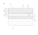
- the optical film F may include the pressure-sensitive adhesive layer 50 arranged on the other side of the transparent base material 10 in the thickness direction D.
- the pressure-sensitive adhesive layer 50 is a layer formed from a pressure-sensitive adhesive composition and has light transmittance.
- the tacky composition contains at least a base polymer that develops tackiness in the pressure-sensitive adhesive layer 50.
- the base polymer include acrylic polymers, rubber-based polymers, silicone-based polymers, urethane-based polymers, polyester-based polymers, and polyamide-based polymers. From the viewpoint of achieving both the adhesive strength required for the pressure-sensitive adhesive layer 50 of the optical film F and high transparency, an acrylic polymer is preferably used as the base polymer.
- the thickness of the pressure-sensitive adhesive layer 50 is preferably 5 ⁇ m or more, more preferably 10 ⁇ m or more, and more preferably 15 ⁇ m or more from the viewpoint of realizing sufficient adhesive force to the adherend in the optical film F. From the viewpoint of ensuring transparency, the thickness of the pressure-sensitive adhesive layer 50 is preferably 300 ⁇ m or less, more preferably 200 ⁇ m or less, still more preferably 100 ⁇ m or less.
- the optical film F shown in FIG. 2 can be manufactured, for example, as follows. First, the adhesive composition is applied onto the release liner to form a coating film. Next, the coating film on the release liner is dried as needed. As a result, the pressure-sensitive adhesive layer 50 is formed on the release liner. Next, the exposed surface of the pressure-sensitive adhesive layer 50 is bonded to the other surface (lower surface in FIG. 1) of the transparent base material 10 of the optical film F shown in FIG. 1 in the thickness direction D. For example, in this way, the optical film F shown in FIG. 2 can be manufactured.
- the optical film F includes the pressure-sensitive adhesive layer 50, no separate adhesive is required when bonding to the adherend.
- the present invention will be specifically described below with reference to examples.
- the present invention is not limited to the examples.
- the specific numerical values such as the compounding amount (content), the physical property value, the parameter, etc. described below are the compounding amounts corresponding to them described in the above-mentioned "form for carrying out the invention” (forms for carrying out the invention). It can be replaced with the upper limit (numerical value defined as “less than or equal to” or “less than”) or lower limit (numerical value defined as "greater than or equal to” or “greater than or equal to”) such as content), physical property value, and parameter.
- an antiglare hard coat layer was formed on one side of a triacetyl cellulose (TAC) film (thickness 80 ⁇ m) as a transparent resin film (hard coat layer forming step).
- TAC triacetyl cellulose
- the main components are Pentaeristol triacrylate, manufactured by Osaka Organic Chemical Industry Co., Ltd.) 50 parts by mass and polymethylmethacrylate particles as antiglare fine particles (trade name "Techpolymer”, average particle diameter 3 ⁇ m, refractive index 1.525, Sekisui Chemicals) (Manufactured by Kogyo Co., Ltd.) 3 parts by mass and silicone particles as antiglare fine particles (trade name "Tospearl 130", average particle diameter 3 ⁇ m, refractive index 1.
- a leveling agent (trade name "LE303", manufactured by Kyoeisha Chemical Co., Ltd.) and a mixed solvent of toluene, ethyl acetate and cyclopentanone (mass ratio 35:41:24) were mixed.
- a composition (crocodile) having a solid content concentration of 55% by mass was prepared.
- An ultrasonic disperser was used for mixing.
- the composition was applied to one side of the TAC film to form a coating film.
- this coating film was cured by irradiation with ultraviolet rays and then dried by heating.
- a high-pressure mercury lamp was used as a light source, ultraviolet rays having a wavelength of 365 nm were used, and the integrated irradiation light amount was set to 300 mJ / cm 2 .
- the heating temperature was 80 ° C., and the heating time was 60 seconds.
- an antiglare hard coat layer (first HC layer) having a thickness of 8 ⁇ m was formed on the TAC film.
- the surface of the HC layer of the TAC film with the HC layer was plasma-treated in a vacuum atmosphere of 1.0 Pa by a roll-to-roll type plasma processing device.
- argon gas was used as the inert gas, and the discharge power was set to 2400 W.
- an adhesion layer and an antireflection layer were sequentially formed on the HC layer of the TAC film with the HC layer after the plasma treatment (sputter film formation step).
- a roll-to-roll sputter film forming apparatus is used to add a 3.5 nm-thick SiOx layer (x ⁇ 2) as an adhesion layer on the HC layer of the TAC film with an HC layer after plasma treatment.
- Nb 2 O 5 layer with a thickness of 12 nm as the first high refractive index layer SiO 2 layer with a thickness of 28 nm as the first low refractive index layer, and Nb 2 with a thickness of 100 nm as the second high refractive index layer.
- a SiO 2 layer having a thickness of 85nm as a second low-refractive index layer are sequentially formed.
- a Si target is used, an argon gas as an inert gas and 3 parts by volume of oxygen gas as a reactive gas with respect to 100 parts by volume of the argon gas are used, and the discharge voltage is set to 520 V.
- the pressure in the film chamber (deposition pressure) was 0.27 Pa, and the SiOx layer (x ⁇ 2) was formed by MFAC sputtering.
- an Nb target is used, 100 parts by volume of argon gas and 5 parts by volume of oxygen gas are used, the discharge voltage is 415 V, the film formation pressure is 0.42 Pa, and Nb is formed by MFAC sputtering. the 2 O 5 layer was formed.
- a Si target is used, 100 parts by volume of argon gas and 30 parts by volume of oxygen gas are used, the discharge voltage is 350 V, the film formation pressure is 0.3 Pa, and SiO is used by MFAC sputtering. Two layers were formed.
- an Nb target is used, 100 parts by volume of argon gas and 13 parts by volume of oxygen gas are used, the discharge voltage is 460 V, the film formation pressure is 0.5 Pa, and Nb is Nb by MFAC sputtering. the 2 O 5 layer was formed.
- a Si target is used, 100 parts by volume of argon gas and 30 parts by volume of oxygen gas are used, the discharge voltage is 340 V, the film formation pressure is 0.25 Pa, and SiO is used by MFAC sputtering. Two layers were formed.
- the antireflection layer (first high refractive index layer, first low refractive index layer, second high refractive index layer, second low) is placed on the HC layer of the TAC film with the HC layer via the adhesion layer.
- the refractive index layer was laminated and formed.
- an antifouling layer was formed on the formed antireflection layer (antifouling layer forming step). Specifically, an antifouling layer having a thickness of 7 nm was formed on the antireflection layer by a vacuum vapor deposition method using an alkoxysilane compound containing a perfluoropolyether group as a vapor deposition source.
- the vapor deposition source is a solid content obtained by drying "Optur UD509" manufactured by Daikin Industries, Ltd. (perfluoropolyether group-containing alkoxysilane compound represented by the above general formula (2), solid content concentration 20% by mass). be.
- the heating temperature of the vapor deposition source in the vacuum vapor deposition method was 260 ° C.
- the optical film of Example 1 was produced.
- the optical film of Example 1 is provided with a transparent base material (resin film, hard coat layer), an adhesion layer, an antireflection layer, and an antifouling layer in this order toward one side in the thickness direction.
- Example 2 Example 1 except that the solid content obtained by drying "Optool UD120" (alkoxysilane compound containing a perfluoropolyether group) manufactured by Daikin Industries, Ltd. was used as the vapor deposition source in the antifouling layer forming step.
- the optical film of Example 2 was produced in the same manner as the optical film of Example 2.
- an antiglare hard coat layer was formed on one side of a triacetyl cellulose (TAC) film (thickness 80 ⁇ m) as a transparent resin film (hard coat layer forming step).
- TAC triacetyl cellulose
- an organosilica sol (trade name "MEK-") containing 100 parts by mass of an ultraviolet curable acrylic monomer (trade name "GRANDIC PC-1070", manufactured by DIC) and nanosilica particles as antiglare fine particles.
- the average primary particle size of the nanosilica particles is 50 nm
- the solid content concentration is 30% by mass, manufactured by Nissan Chemical Co., Ltd.) 1.5 parts by mass of synthetic smectite, which is an organic clay, manufactured by Corp Chemical Co., Ltd., 3 parts by mass of a photopolymerization initiator (trade name "OMNIRAD907", manufactured by BASF), and a leveling agent (trade name "LE303", Kyoeisha Chemical Co., Ltd.)
- a composition (crocodile) having a solid content concentration of 55% by mass was prepared by mixing with 0.15 parts by mass. An ultrasonic disperser was used for mixing. Next, the composition was applied to one side of the TAC film to form a coating film.
- this coating film was cured by irradiation with ultraviolet rays and then dried by heating.
- a high-pressure mercury lamp was used as a light source, ultraviolet rays having a wavelength of 365 nm were used, and the integrated irradiation light amount was set to 200 mJ / cm 2 .
- the heating time was 80 ° C., and the heating temperature was 3 minutes.
- an antiglare hard coat layer (second HC layer) having a thickness of 6 ⁇ m was formed on the TAC film.
- the surface of the HC layer of the TAC film with the HC layer was plasma-treated in a vacuum atmosphere of 1.0 Pa by a roll-to-roll type plasma processing device.
- argon gas was used as the inert gas, and the discharge power was set to 150 W.
- an adhesion layer and an antireflection layer were sequentially formed on the HC layer of the TAC film with the HC layer after the plasma treatment (sputter film formation step).
- a roll-to-roll sputter film forming apparatus is used to form an indium tin oxide (ITO) layer having a thickness of 1.5 nm as an adhesion layer on the HC layer of the TAC film with an HC layer after plasma treatment.
- ITO indium tin oxide
- Nb 2 O 5 layer with a thickness of 12 nm as the first high refractive index layer SiO 2 layer with a thickness of 28 nm as the first low refractive index layer
- Nb with a thickness of 100 nm as the second high refractive index layer.
- a SiO 2 layer having a thickness of 85nm as a second low-refractive index layer are sequentially formed.
- an ITO target is used, an argon gas as an inert gas and 10 parts by volume of oxygen gas as a reactive gas with respect to 100 parts by volume of the argon gas are used, and the discharge voltage is set to 400 V.
- the pressure in the film chamber (deposition pressure) was 0.2 Pa, and the ITO layer was formed by MFAC sputtering.
- the conditions for forming the first high refractive index layer, the first low refractive index layer, the second high refractive index layer, and the second low refractive index layer in the present embodiment are the first high refractive index layer and the first in the first embodiment.
- the conditions for forming the low refractive index layer, the second high refractive index layer, and the second low refractive index layer are the same as described above.
- an antifouling layer was formed on the formed antireflection layer (antifouling layer forming step). Specifically, it is the same as the antifouling layer forming step in Example 1 (as a vapor deposition source, a solid content obtained by drying "Optur UD509" manufactured by Daikin Industries, Ltd. was used).
- the optical film of Example 3 was produced.
- the optical film of Example 3 is provided with a transparent base material (resin film, hard coat layer), an adhesion layer, an antireflection layer, and an antifouling layer in this order toward one side in the thickness direction.
- Example 4 Example 3 except that the solid content obtained by drying "Optool UD120" (alkoxysilane compound containing a perfluoropolyether group) manufactured by Daikin Industries, Ltd. was used as the vapor deposition source in the antifouling layer forming step.
- the optical film of Example 4 was produced in the same manner as the optical film of Example 4.
- Example 5 This was carried out except that the solid content obtained by drying "KY-1901" (alkoxysilane compound containing a perfluoropolyether group) manufactured by Shin-Etsu Chemical Co., Ltd. was used as the vapor deposition source in the antifouling layer forming step.
- the optical film of Example 5 was produced in the same manner as the optical film of Example 3.
- Example 6 The optical film of Example 6 was produced in the same manner as the optical film of Example 3 except for the hard coat layer forming step and the antifouling layer forming step.
- the acrylic monomer composition containing nanosilica particles (trade name “NC035”, the average primary particle diameter of the nanosilica particles is 40 nm, the solid content concentration is 50% by mass, and the nanosilica in the solid content.
- the ratio of particles is 60% by mass, 67 parts by mass of Arakawa Chemical Industry Co., Ltd., and 33 parts by mass of ultraviolet curable polyfunctional acrylate (trade name "Binder A”, solid content concentration 100% by mass, manufactured by Arakawa Chemical Industry Co., Ltd.).
- polymethylmethacrylate particles as antiglare fine particles (trade name "Techpolymer”, average particle diameter 3 ⁇ m, refractive index 1.525, manufactured by Sekisui Kasei Kogyo Co., Ltd.), and silicone as antiglare fine particles.
- Particles (trade name "Tospearl 130", average particle diameter 3 ⁇ m, refractive index 1.42, manufactured by Momentive Performance Materials Japan) 1.5 parts by mass and thixotropy-imparting agent (trade name "Lucentite SAN", 1.5 parts by mass of synthetic smectite, which is an organic clay, manufactured by Corp Chemical Co., Ltd., 3 parts by mass of a photopolymerization initiator (trade name "OMNIRAD907", manufactured by BASF), and a leveling agent (trade name "LE303", Kyoeisha Chemical Co., Ltd.)
- a composition (crocodile) having a solid content concentration of 45% by mass was prepared by mixing 0.15 parts by mass and toluene.
- An ultrasonic disperser was used for mixing.
- the composition was applied to one side of the TAC film to form a coating film.
- this coating film was cured by irradiation with ultraviolet rays and then dried by heating.
- a high-pressure mercury lamp was used as a light source, ultraviolet rays having a wavelength of 365 nm were used, and the integrated irradiation light amount was set to 200 mJ / cm 2 .
- the heating time was 60 ° C., and the heating temperature was 60 seconds.
- an antiglare hard coat layer (third HC layer) having a thickness of 7 ⁇ m was formed on the TAC film.
- Example 6 a solid content obtained by drying "Optur UD120" (alkoxysilane compound containing a perfluoropolyether group) manufactured by Daikin Industries, Ltd. was used as a vapor deposition source.
- Example 7 This was carried out except that the solid content obtained by drying "KY-1901" (alkoxysilane compound containing a perfluoropolyether group) manufactured by Shin-Etsu Chemical Co., Ltd. was used as the vapor deposition source in the antifouling layer forming step.
- the optical film of Example 7 was produced in the same manner as the optical film of Example 6.
- Example 8 The optical film of Example 8 was produced in the same manner as the optical film of Example 3 except for the hard coat layer forming step and the antifouling layer forming step.
- the acrylic monomer composition containing nanosilica particles (trade name “NC035HS”, the average primary particle diameter of the nanosilica particles is 40 nm, the solid content concentration is 50% by mass, and the nanosilica in the solid content. Particle ratio is 60% by mass, manufactured by Arakawa Chemical Industry Co., Ltd.
- UV curable polyfunctional urethane acrylate (trade name "Beamset 580", solid content concentration 70% by mass, manufactured by Arakawa Chemical Industry Co., Ltd.) 17 4 parts by mass and 4 parts by mass of polymethylmethacrylate particles (trade name "Techpolymer”, average particle diameter 3 ⁇ m, refractive index 1.495, manufactured by Sekisui Kasei Kogyo Co., Ltd.) as antiglare fine particles, and as antiglare fine particles Silicone particles (trade name "Tospearl 130", average particle diameter 3 ⁇ m, refractive index 1.42, manufactured by Momentive Performance Materials Japan Co., Ltd.) 0.1 part by mass and thixotropy-imparting agent (trade name "Lucentite SAN”) , 2.0 parts by mass of synthetic smectite, which is an organic clay, manufactured by Coop Chemical Co., Ltd., 3 parts by mass of a photopolymerization initiator (trade name "OMNIRAD907", manufactured by
- An ultrasonic disperser was used for mixing.
- the composition was applied to one side of the TAC film to form a coating film.
- this coating film was cured by irradiation with ultraviolet rays and then dried by heating.
- a high-pressure mercury lamp was used as a light source, ultraviolet rays having a wavelength of 365 nm were used, and the integrated irradiation light amount was set to 200 mJ / cm 2 .
- the heating time was 60 ° C., and the heating temperature was 60 seconds.
- an antiglare hard coat layer fourth HC layer having a thickness of 8 ⁇ m was formed on the TAC film.
- Example 8 a solid content obtained by drying "KY-1903-1" (alkoxysilane compound containing a perfluoropolyether group) manufactured by Shin-Etsu Chemical Co., Ltd. is used as a vapor deposition source. board.
- Comparative Example 1 The optical film of Comparative Example 1 was produced in the same manner as the optical film of Example 1 except for the antifouling layer forming step.
- ⁇ Water contact angle> The water contact angle on the surface of the antifouling layer was examined for each of the optical films of Examples 1 to 8 and Comparative Example 1. First, water droplets were formed on the surface of the antifouling layer of the optical film by dropping about 1 ⁇ L of pure water. Next, the angle formed by the surface of the water droplet on the surface of the antifouling layer and the surface of the antifouling layer was measured. A contact angle meter (trade name "DMo-501", manufactured by Kyowa Interface Science Co., Ltd.) was used for the measurement. The measurement results are shown in Table 1.
- ⁇ Surface roughness Ra> The surface roughness Ra of the antifouling layer was examined for each of the optical films of Examples 1 to 8 and Comparative Example 1. Specifically, the surface of the antifouling layer of each optical film is observed with an atomic force microscope (trade name "SPI3800", manufactured by Seiko Instruments, Inc.), and the surface roughness Ra (arithmetic mean roughness) is observed in a 1 ⁇ m square observation image. I asked for it. The results are shown in Table 1.
- the transparent base material side of the sample film (50 mm ⁇ 50 mm) cut out from the optical film was attached to a black acrylic plate via an adhesive.
- total reflection measurement was performed on the sample bonded to the black acrylic plate using a spectrophotometer (trade name "U-4100", manufactured by Hitachi High-Technologies Corporation). Based on the spectral reflectance at a wavelength of 380 to 780 nm obtained by this measurement and the relative spectral distribution of the CIE standard Illuminant D65, the three stimuli of the object color due to reflection in the XYZ color system defined by JIS Z8701. The value Y was calculated and the total reflection Y value was obtained.
- the scattered light was removed by using a spectrophotometer (trade name "U-4100") and the jig attached to the U-4100. Specular reflection measurement was performed under the condition of an incident angle of 5 °. Based on the spectral reflectance at a wavelength of 380 to 780 nm obtained by this measurement and the relative spectral distribution of the CIE standard Illuminant D65, the three stimuli of the object color due to reflection in the XYZ color system defined by JIS Z8701. The value Y was calculated and the normal reflection Y value was obtained.
- the ratio of (Y 2 / Y 1 ) is shown in Table 1.
- ⁇ Surface haze> The surface haze of each of the optical films of Examples 1 to 8 and Comparative Example 1 was examined. Specifically, first, the sample film cut out from the optical film was subjected to haze measurement based on JIS K 7136 (2000) using "Haze Meter HM150" manufactured by Murakami Color Technology Research Institute (this). Measures the total haze value of the sample film). Next, in a state where the cycloolefin polymer film was attached to the surface of the sample film on the antifouling layer side via an adhesive to eliminate the surface haze of the sample film, the "haze meter HM150" manufactured by Murakami Color Technology Research Institute was used.
- the antifouling property of the antifouling layer was examined for each of the optical films of Examples 1 to 8 and Comparative Example 1. Specifically, first, the surface of the antifouling layer of the optical film was touched with a finger to attach a fingerprint. Next, the fingerprint was wiped with a cotton cloth (work of sweeping the waste in one direction while bringing the waste into contact with the area including the fingerprint adhesion portion on the surface of the antifouling layer) three times. Then, regarding the antifouling property of the antifouling layer, the case where the fingerprint is wiped off by three wiping operations is evaluated as "good", and the case where the fingerprint is not wiped off even after three wiping operations (that is, a part of the fingerprint). (If remains) was evaluated as "defective”. The results are shown in Table 1.
- the optical film with an antifouling layer of the present invention can be applied to, for example, an antireflection film with an antifouling layer, a transparent conductive film with an antifouling layer, and an electromagnetic wave shielding film with an antifouling layer.
- Optical film (optical film with antifouling layer) 10 Transparent base material 11 Resin film 12 Hard coat layer 20 Optical functional layer 21 First high refractive index layer 22 First low refractive index layer 23 Second high refractive index layer 24 Second low refractive index layer 30 Antifouling layer 31 Outer surface 40 Adhesive layer 50 Adhesive layer
Landscapes
- Physics & Mathematics (AREA)
- Chemical & Material Sciences (AREA)
- Engineering & Computer Science (AREA)
- Optics & Photonics (AREA)
- General Physics & Mathematics (AREA)
- Mechanical Engineering (AREA)
- Chemical Kinetics & Catalysis (AREA)
- Inorganic Chemistry (AREA)
- Organic Chemistry (AREA)
- Metallurgy (AREA)
- Materials Engineering (AREA)
- Health & Medical Sciences (AREA)
- Manufacturing & Machinery (AREA)
- Ophthalmology & Optometry (AREA)
- Laminated Bodies (AREA)
- Surface Treatment Of Optical Elements (AREA)
Abstract
本発明の光学フィルム(F)は、透明基材(10)と、光学機能層(20)と、防汚層(30)とをこの順で備える防汚層付き光学フィルムである。防汚層(30)における光学機能層(20)とは反対側の外表面(31)は、110°以上の水接触角を有する。
Description
本発明は、防汚層付き光学フィルムに関する。
液晶ディスプレイなどのディスプレイにおける画像表示側の外表面には、例えば、所定の光学的機能を有する層(光学機能層)を備える透明な光学フィルムが設けられる。光学フィルムとしては、例えば、反射防止フィルム、透明導電性フィルム、および電磁波遮蔽フィルムが挙げられる。光学フィルムは、例えば、透明基材と、その一方面側に配置されている光学機能層と、透明基材の他方面上に配置されている粘着剤層とを備える。このような光学フィルムに関する技術については、例えば下記の特許文献1に記載されている。
光学機能層が最表層として配置されている光学フィルムでは、手脂などの汚染物質が光学機能層に付着しやすく、また、付着した汚染物質が光学機能層から除去されにくい。光学フィルムにおける汚染物質の付着は、光学フィルムの透明性の確保の観点から好ましくない。そのため、光学フィルムには、例えば、防汚層が最表層として設けられる。そのような防汚層付き光学フィルムでは、防汚層において高い防汚性が求められる。
本発明は、防汚層において高い防汚性を実現するのに適した防汚層付き光学フィルムを提供する。
本発明[1]は、透明基材と、光学機能層と、防汚層とをこの順で備え、防汚層における光学機能層とは反対側の外表面が、110°以上の水接触角を有する、防汚層付き光学フィルムを含む。
本発明[2]は、前記外表面が、2nmを超える表面粗さRaを有する、上記[1]に記載の防汚層付き光学フィルムを含む。
本発明[3]は、光学機能層が反射防止層である、上記[1]または[2]に記載の防汚層付き光学フィルムを含む。
本発明[4]は、反射防止層が、相対的に屈折率が大きな高屈折率層と、相対的に屈折率が小さな低屈折率層とを交互に含む、上記[3]に記載の防汚層付き光学フィルムを含む。
本発明[5]は、透明基材が、光学機能層側にハードコート層を有する、上記[1]から[4]いずれか一つに記載の防汚層付き光学フィルムを含む。
本発明[6]は、ハードコート層が金属酸化物微粒子を含有する、上記[5]に記載の防汚層付き光学フィルムを含む。
本発明[7]は、金属酸化物微粒子がナノシリカ粒子である、上記[6]に記載の防汚層付き光学フィルムを含む。
本発明[8]は、ハードコート層における光学機能層側の表面が、0.5nm以上20nm以下の表面粗Raさを有する、上記[5]から[7]のいずれか一つに記載の防汚層付き光学フィルムを含む。
本発明の防汚層付き光学フィルムは、防汚層における光学機能層とは反対側の外表面が110°以上の水接触角を有することから、防汚層において高い防汚性を実現するのに適する。
本発明の防汚層付き光学フィルムの一実施形態としての光学フィルムFは、図1に示すように、透明基材10と、光学機能層20と、防汚層30とを、厚さ方向Dの一方側に向かってこの順で備える。光学フィルムFは、本実施形態では、透明基材10と、密着層40と、光学機能層20と、防汚層30とを、厚さ方向Dの一方側に向かってこの順で備え、好ましくは、透明基材10と、密着層40と、光学機能層20と、防汚層30とからなる。また、光学フィルムFは、厚さ方向Dに直交する方向(面方向)に広がる形状を有する。
透明基材10は、本実施形態では、樹脂フィルム11と、ハードコート層12とを厚さ方向Dの一方側に向かってこの順で備える。
樹脂フィルム11は、可撓性を有する透明な樹脂フィルムである。樹脂フィルム11の材料としては、例えば、ポリエステル樹脂、ポリオレフィン樹脂、ポリスチレン樹脂、アクリル樹脂、ポリカーボネート樹脂、ポリエーテルスルホン樹脂、ポリスルホン樹脂、ポリアミド樹脂、ポリイミド樹脂、セルロース樹脂、ノルボルネン樹脂、ポリアリレート樹脂、およびポリビニルアルコール樹脂が挙げられる。ポリエステル樹脂としては、例えば、ポリエチレンテレフタレート(PET)、ポリブチレンテレフタレート、およびポリエチレンナフタレートが挙げられる。ポリオレフィン樹脂としては、例えば、ポリエチレン、ポリプロピレン、およびシクロオレフィンポリマーが挙げられる。セルロース樹脂としては、例えば、トリアセチルセルロースが挙げられる。これら材料は、単独で用いられてもよいし、二種類以上が併用されてもよい。透明性および強度の観点から、樹脂フィルム11の材料としては、好ましくはセルロース樹脂が用いられ、より好ましくはトリアセチルセルロースが用いられる。
樹脂フィルム11におけるハードコート層12側表面は、表面改質処理されていてもよい。表面改質処理としては、例えば、コロナ処理、プラズマ処理、オゾン処理、プライマー処理、グロー処理、およびカップリング剤処理が挙げられる。
樹脂フィルム11の厚さは、強度の観点から、好ましくは5μm以上、より好ましくは10μm以上、さらに好ましくは20μm以上である。樹脂フィルム11の厚さは、取扱い性の観点から、好ましくは300μm以下、より好ましくは200μm以下である。
樹脂フィルム11の可視光透過率は、透明性の観点から、好ましくは80%以上、より好ましくは90%以上である。樹脂フィルム11の可視光透過率は、例えば100%以下である。
ハードコート層12は、樹脂フィルム11の厚さ方向D一方面上に配置されている。ハードコート層12は、光学フィルムFの露出表面(図1では上面)に擦り傷が形成されにくくするための層である。
ハードコート層12は、硬化性樹脂組成物の硬化物である。硬化性樹脂組成物が含有する硬化性樹脂としては、例えば、ポリエステル樹脂、アクリル樹脂、ウレタン樹脂、アクリルウレタン樹脂、アミド樹脂、シリコーン樹脂、エポキシ樹脂、およびメラミン樹脂が挙げられる。これら硬化性樹脂は、単独で用いられてもよいし、二種類以上が併用されてもよい。ハードコート層12の高硬度の確保の観点からは、硬化性樹脂としては、好ましくは、アクリル樹脂および/またはアクリルウレタン樹脂が用いられる。
また、硬化性樹脂組成物としては、例えば、紫外線硬化型の樹脂組成物、および、熱硬化型の樹脂組成物が挙げられる。高温加熱せずに硬化可能であるために光学フィルムFの製造効率向上に役立つ観点から、硬化性樹脂組成物としては、好ましくは、紫外線硬化型の樹脂組成物が用いられる。紫外線硬化型の樹脂組成物には、紫外線硬化型モノマー、紫外線硬化型オリゴマー、および紫外線硬化型ポリマーからなる群より選択される少なくとも一種類が含まれる。紫外線硬化型の樹脂組成物としては、例えば、特開2016-179686号公報に記載のハードコート層形成用組成物が挙げられる。
ハードコート層12は、防眩性を有するハードコート層(防眩性ハードコート層)であってもよい。防眩性ハードコート層としてのハードコート層12は、硬化性樹脂(マトリックス樹脂)と、防眩性を発現させるための微粒子(防眩性微粒子)と、を含有する硬化性樹脂組成物の硬化物である。防眩性微粒子としては、例えば、金属酸化物微粒子および有機系微粒子が挙げられる。金属酸化物微粒子の材料としては、例えば、シリカ、アルミナ、チタニア、ジルコニア、酸化カルシウム、酸化錫、酸化インジウム、酸化カドミウ、および酸化アンチモンが挙げられる。有機系微粒子の材料としては、ポリメチルメタクリレート、シリコーン、ポリスチレン、ポリウレタン、アクリル-スチレン共重合体、ベンゾグアナミン、メラミン、およびポリカーボネートが挙げられる。これら微粒子は、単独で用いられてもよいし、二種類以上が併用されてもよい。ハードコート層12において良好な防眩性を発現させる観点からは、防眩性微粒子としては、好ましくは、ナノシリカ粒子、ポリメチルメタクリレート粒子、およびシリコーン粒子からなる群より選択される少なくとも一種類が用いられる。
微粒子の平均粒子径は、例えば10μm以下、好ましくは8μm以下であり、また、例えば1nm以上である。微粒子としてナノ粒子を用いる場合、当該微粒子の平均粒子径は、例えば100nm以下であり、好ましくは70nm以下であり、また、例えば1nm以上である。微粒子の平均粒子径は、例えば、レーザー散乱法における粒度分布測定法によって求められた粒度分布に基づいて、D50値(累積50%メジアン径)として求められる。
マトリックス樹脂(硬化後)の屈折率は、例えば1.46以上であり、好ましくは1.49以上、より好ましくは1.50以上、さらに好ましくは1.51以上である。同屈折率は、例えば1.60以下であり、好ましくは1.59以下、より好ましくは1.58以下、さらに好ましくは1.57以下である。
微粒子の屈折率は、マトリックス樹脂の上記屈折率よりも高くてもよいし、低くてもよい。微粒子の屈折率がマトリックス樹脂の屈折率よりも高い場合、微粒子の屈折率は、例えば1.62以下であり、好ましくは1.60以下、より好ましくは1.59以下、さらに好ましくは1.50以下である。微粒子の屈折率がマトリックス樹脂の屈折率よりも低い場合、微粒子の屈折率は、例えば1.40以上であり、好ましくは1.42以上、より好ましくは1.44以上である。
ハードコート層12における微粒子の含有量は、マトリックス樹脂100質量部に対し、好ましくは1質量部以上であり、より好ましくは3質量部以上である。ハードコート層12における微粒子の含有量は、マトリックス樹脂100質量部に対し、好ましくは30質量部以下であり、より好ましくは20質量部以下である。
ハードコート層12の厚さは、同層の硬度確保の観点からは、好ましくは0.5μm以上、より好ましくは1μm以上である。ハードコート層12の厚さは、例えば10μm以下である。
ハードコート層12における密着層40側表面は、表面改質処理されていてもよい。表面改質処理としては、例えば、プラズマ処理、コロナ処理、オゾン処理、プライマー処理、グロー処理、およびカップリング剤処理が挙げられる。ハードコート層12と密着層40との間において高い密着力を確保する観点からは、ハードコート層12における密着層40側表面は、好ましくはグロー処理されている。
透明基材10の厚さは、強度の観点から、好ましくは5μm以上、より好ましくは10μm以上、さらに好ましくは20μm以上である。透明基材10の厚さは、取扱い性の観点から、好ましくは300μm以下、より好ましくは200μm以下である。
透明基材10の可視光透過率は、透明性の観点から、好ましくは80%以上、より好ましくは90%以上である。透明基材10の可視光透過率は、例えば100%以下である。
透明基材10における光学機能層20側の表面(本実施形態では、ハードコート層12における光学機能層20側の表面)の表面粗さRa(算術平均表面粗さ)は、好ましくは0.5nm以上、より好ましくは0.8nm以上である。同表面粗さRaは、好ましくは20nm以下、より好ましくは15nm以下である。表面粗さRaは、例えば、AFM(原子間力顕微鏡)による1μm四方の観察像から求められる。
密着層40は、透明基材10と、光学機能層20との、密着力を確保するための層である。密着層40は、透明基材10(本実施形態において具体的には、透明基材10のハードコート層12)の厚さ方向D一方面上に配置されている。密着層40の材料としては、例えば、シリコン、ニッケル、クロム、アルミニウム、錫、金、銀、白金、亜鉛、チタン、タングステン、ジルコニウム、パラジウム等の金属、これら金属の2種類以上の合金、および、これら金属の酸化物が挙げられる。有機層(具体的にはハードコート層12)および酸化物層(具体的には、後記の第1高屈折率層21)の両方に対する密着性と、密着層40の透明性との両立の観点からは、密着層40の材料としては、好ましくは酸化シリコン(SiOx)またはインジウムスズ酸化物(ITO)が用いられる。密着層40の材料として酸化シリコンが用いられる場合、好ましくは、化学量論組成よりも酸素量の少ないSiOxが用いられ、より好ましくは、xが1.2以上1.9以下のSiOxが用いられる。
密着層40の厚さは、透明基材10と光学機能層20との間の密着力の確保と、密着層40の透明性との両立の観点から、例えば1nm以上であり、また、例えば10nm以下である。
光学機能層20は、密着層40の厚さ方向D一方面上に配置されている。本実施形態では、光学機能層20は、外光の反射強度を抑制するための反射防止層である。すなわち、光学フィルムFは、本実施形態では反射防止フィルムである。
光学機能層20(反射防止層)は、相対的に屈折率が大きな高屈折率層と、相対的に屈折率が小さな低屈折率層とを、厚さ方向に交互に有する。反射防止層では、それに含まれる複数の薄層(高屈折率層,低屈折率層)における複数の界面での反射光間の干渉作用により、正味の反射光強度が減衰される。また、反射防止層では、各薄層の光学膜厚(屈折率と厚さとの積)の調整により、反射光強度を減衰させる干渉作用を発現させることができる。このような反射防止層としての光学機能層20は、本実施形態において具体的には、第1高屈折率層21と、第1低屈折率層22と、第2高屈折率層23と、第2低屈折率層24とを、厚さ方向Dの一方側に向かってこの順で有する。
第1高屈折率層21および第2高屈折率層23は、それぞれ、波長550nmにおける屈折率が好ましくは1.9以上の高屈折率材料からなる。高屈折率と可視光の低吸収性との両立の観点から、高屈折率材料としては、例えば、酸化ニオブ(Nb2O5)、酸化チタン、酸化ジルコニウム、スズドープ酸化インジウム(ITO)、およびアンチモンドープ酸化スズ(ATO)が挙げられ、好ましくは酸化ニオブが用いられる。
第1高屈折率層21の光学膜厚(屈折率と厚さとの積)は、例えば20nm以上であり、また、例えば55nm以下である。第2高屈折率層23の光学膜厚は、例えば60nm以上であり、また、例えば330nm以下である。
第1低屈折率層22および第2低屈折率層24は、それぞれ、波長550nmにおける屈折率が好ましくは1.6以下の低屈折率材料からなる。低屈折率と可視光の低吸収性との両立の観点から、低屈折率材料としては、例えば、二酸化ケイ素(SiO2)およびフッ化マグネシウムが挙げられ、好ましくは二酸化ケイ素が用いられる。第2低屈折率層24の材料としては、第2低屈折率層24と防汚層30との密着性確保の観点からも、好ましくは二酸化ケイ素が用いられる。
第1低屈折率層22の光学膜厚は、例えば15nm以上であり、また、例えば70nm以下である。第2低屈折率層24の光学膜厚は、例えば100nm以上であり、また、例えば160nm以下である。
また、光学機能層20において、第1高屈折率層21の厚さは、例えば1nm以上、好ましくは5nm以上であり、また、例えば30nm以下、好ましくは20nm以下である。第1低屈折率層22の厚さは、例えば10nm以上、好ましくは20nm以上であり、また、例えば50nm以下、好ましくは30nm以下である。第2高屈折率層23の厚さは、例えば50nm以上、好ましくは80nm以上であり、また、例えば200nm以下、好ましくは150nm以下である。第2低屈折率層24の厚さは、例えば60nm以上、好ましくは80nm以上であり、また、例えば150nm以下、好ましくは100nm以下である。
防汚層30は、光学フィルムFにおける防汚機能を有する層であり、光学機能層20の厚さ方向D一方面上に配置されている。防汚層30は、厚さ方向D一方側に外表面31を有する。防汚層30の防汚機能には、光学フィルムFの使用時のフィルム露出面に対する手脂などの汚染物質の付着の抑制機能、および、付着した汚染物質を除去しやすくする機能が含まれる。
防汚層30の材料としては、例えば、フッ素基含有の有機化合物が挙げられる。フッ素基含有の有機化合物としては、好ましくは、パーフルオロポリエーテル基を有するアルコキシシラン化合物が用いられる。パーフルオロポリエーテル基を有するアルコキシシラン化合物としては、例えば、下記の一般式(1)で表される化合物が挙げられる。
R1-R2-X-(CH2)m-Si(OR3)3 (1)
一般式(1)において、R1は、アルキル基における一つ以上の水素原子がフッ素原子に置換された、直鎖状または分岐状のフッ化アルキル基(炭素数は例えば1以上20以下)を表し、好ましくは、アルキル基の水素原子のすべてがフッ素原子に置換されたパーフルオロアルキル基を表す。
R2は、パーフルオロポリエーテル(PFPE)基の繰り返し構造を少なくとも一つ含む構造を表し、好ましくは、PFPE基の繰り返し構造を二つ含む構造を表す。PFPE基の繰り返し構造としては、例えば、直鎖状PFPE基の繰り返し構造、および、分岐状PFPE基の繰り返し構造が挙げられる。直鎖状PFPE基の繰り返し構造としては、例えば、-(OCnF2n)p-で表される構造(nは、1以上20以下の整数を表し、pは、1以上50以下の整数を表す。以下同じ)が挙げられる。分岐状PFPE基の繰り返し構造としては、例えば、-(OC(CF3)2)p-で表される構造、および、-(OCF2CF(CF3)CF2)p-で表される構造が挙げられる。PFPE基の繰り返し構造としては、好ましくは、直鎖状PFPE基の繰り返し構造が挙げられ、より好ましくは、-(OCF2)p-および-(OC2F4)p-が挙げられる。
R3は、炭素数1以上4以下アルキル基を表し、好ましくはメチル基を表す。
Xは、エーテル基、カルボニル基、アミノ基、またはアミド基を表し、好ましくはエーテル基を表す。
mは、1以上の整数を表す。また、mは、好ましくは20以下、より好ましくは10以下、さらに好ましくは5以下の整数を表す。
このようなパーフルオロポリエーテル基を有するアルコキシシラン化合物のうち、好ましくは、下記の一般式(2)に示される化合物が用いられる。
CF3-(OCF2)q-(OC2F4)r-O-(CH2)3-Si(OCH3)3 (2)
一般式(2)において、qは、1以上50以下の整数を表し、rは、1以上50以下の整数を表す。
また、パーフルオロポリエーテル基を有するアルコキシシラン化合物は、単独で用いられてもよいし、二種類以上が併用されてもよい。
防汚層30は、本実施形態では、ドライコーティング法で形成された膜(ドライコーティング膜)である。ドライコーティング法としては、スパッタリング法、真空蒸着法、およびCVDが挙げられる。防汚層30は、好ましくはドライコーティング膜であり、より好ましくは真空蒸着膜である。
防汚層30の材料が、パーフルオロポリエーテル基を有するアルコキシシラン化合物を含有し、且つ、防汚層30が、ドライコーティング膜(好ましくは真空蒸着膜)である構成は、光学機能層20に対する防汚層30の高い接合力の確保に適し、従って、防汚層30の耐剥離性の確保に適する。防汚層30の耐剥離性が高いことは、防汚層30の防汚性能の維持に役立つ。
防汚層30の厚さは、好ましくは1nm以上、より好ましくは2nm以上、さらに好ましくは3nm以上である。防汚層30の厚さは、好ましくは100nm以下、より好ましくは50nm以下、さらに好ましくは30nm以下である。
防汚層30の外表面31の水接触角(純水接触角)は、110°以上であり、好ましくは111°以上、より好ましくは112°以上、さらに好ましくは113°以上、特に好ましくは114°以上である。外表面31における水接触角がこの程度に高い構成は、防汚層30において高い防汚性を実現するのに適する。同水接触角は、例えば130°以下である。水接触角は、防汚層30の外表面31(露出表面)に直径2mm以下の水滴(純水の液滴)を形成して、防汚層30表面に対する当該水滴の接触角を測定することにより、求められる。外表面31の水接触角は、例えば、防汚層30の組成、外表面31の粗さ、ハードコート層12の組成、および、ハードコート層12の光学機能層20側の表面の粗さの調整によって、調整できる。
防汚層30の外表面31の表面粗さRa(算術平均表面粗さ)は、好ましくは1nm以上、より好ましくは1.3nm以上、さらに好ましくは2nm以上である。このような構成は、防汚層30の外表面31の光沢感が強くなりすぎるのを回避するのに適する。同表面粗さRaは、好ましくは20nm以下、より好ましくは18nm以下、さらに好ましくは17nm以下である。このような構成は、光学フィルムFにおける光学特性とヘイズの観点から好ましく、例えば、光学フィルムFがディスプレイ表面に設けられる場合に、当該光学フィルムFを介して視認される画像の白ボケ(white blurring)を抑制するのに適する。
防汚層30の全反射Y値は、好ましくは1以下、より好ましくは0.9以下である。防汚層30の正反射Y値は、好ましくは0.9以下、より好ましくは0.8以下である。これら構成は、光学フィルムFがディスプレイ表面に設けられる場合に、当該でスプレイ表面での背景の映り込みを抑制するのに適する。
全反射Y値(Y1)と正反射Y値(Y2)との差ΔY(Y1-Y2)は、好ましくは0.13を超え、より好ましくは0.15以上、さらに好ましくは0.17以上である。このような構成は、防汚層30ないし光学フィルムFの防眩性を確保するのに適する。差ΔYは、好ましくは0.8以下、より好ましくは0.7以下である。このような構成は、光学フィルムFがディスプレイ表面に設けられる場合に、当該光学フィルムFを介して視認される画像の白ボケを抑制するのに適する。
全反射Y値(Y1)に対する正反射Y値(Y2)の比率(Y2/Y1)は、好ましくは0.15以上、より好ましくは0.18以上である。このような構成は、光学フィルムFがディスプレイ表面に設けられる場合に、当該光学フィルムFを介して視認される画像の白ボケを抑制するのに適する。同比率(Y2/Y1)は、好ましくは0.6以下、より好ましくは0.58以下である。このような構成は、防汚層30ないし光学フィルムFの防眩性を確保するのに適する。
防汚層30の表面ヘイズ(外部ヘイズ)は、好ましくは20%以下、より好ましくは10%以下である。このような構成は、光学フィルムFの透明性を確保するのに適する。防汚層30の表面ヘイズは、例えば0.01%以上である。
光学フィルムFは、透明基材10を用意した後、例えばロールトゥロール方式において、透明基材10上に密着層40、光学機能層20、および防汚層30を順次に積層することによって、作製できる。光学機能層20は、密着層40上に第1高屈折率層21、第1低屈折率層22、第2高屈折率層23、および第2低屈折率層24を順次に積層することによって形成できる。
透明基材10は、樹脂フィルム11上にハードコート層12を形成することによって作製できる。ハードコート層12は、例えば、樹脂フィルム11上に、硬化性樹脂と必要に応じて防眩性微粒子とを含有する硬化性樹脂組成物を塗布して塗膜を形成した後、この塗膜を硬化させることによって形成できる。硬化性樹脂組成物が紫外線化型樹脂を含有する場合には、紫外線照射によって前記塗膜を硬化させる。硬化性樹脂組成物が熱硬化型樹脂を含有する場合には、加熱によって前記塗膜を硬化させる。
透明基材10上に形成されたハードコート層12の露出表面は、必要に応じて、表面改質処理される。表面改質処理としてプラズマ処理する場合、不活性ガスとして例えばアルゴンガスを用いる。また、プラズマ処理における放電電力は、例えば10W以上であり、また、例えば10000W以下である。
密着層40、第1高屈折率層21、第1低屈折率層22、第2高屈折率層23、および第2低屈折率層24は、それぞれ、ドライコーティング法で材料を成膜することによって形成できる。ドライコーティング法としては、スパッタリング法、真空蒸着法、およびCVDが挙げられ、好ましくはスパッタリング法が用いられる。
スパッタリング法では、スパッタ室内に真空条件下でガスを導入しつつ、カソード上に配置されたターゲットにマイナスの電圧を印加する。これにより、グロー放電を発生させてガス原子をイオン化し、当該ガスイオンを高速でターゲット表面に衝突させ、ターゲット表面からターゲット材料を弾き出し、弾き出たターゲット材料を所定面上に堆積させる。金属酸化物層を形成するには、成膜速度の観点から、反応性スパッタリングが好ましい。反応性スパッタリングでは、ターゲットとして金属ターゲットを用い、上述のガスとして、アルゴンなどの不活性ガスと酸素(反応性ガス)との混合ガスを用いる。不活性ガスと酸素との流量比(sccm)の調整により、成膜される金属酸化物層に含まれる酸素の割合を調整できる。
スパッタリング法を実施するための電源としては、例えば、DC電源、AC電源、RF電源、および、MFAC電源(周波数帯が数十~数百MHzのAC電源)が挙げられる。スパッタリング法における放電電圧は、例えば200V以上であり、また、例えば1000V以下である。また、スパッタリング法が実施されるスパッタ室内の成膜気圧は、例えば0.01Pa以上であり、また、例えば2Pa以下である。
防汚層30は、光学機能層20上に例えばフッ素基含有の有機化合物を成膜することによって形成できる。防汚層30の形成手法としては、ドライコーティング法が挙げられる。ドライコーティング法としては、例えば、真空蒸着法、スパッタリング法、およびCVDが挙げられ、好ましくは真空蒸着法が用いられる。
例えば以上のようにして、光学フィルムFを製造できる。光学フィルムFは、透明基材10側が例えば粘着剤を介して被着体に貼り合わされて、使用される。
光学フィルムFは、反射防止フィルム以外の他の光学フィルムであってもよい。他の光学フィルムとしては、例えば、透明導電性フィルムおよび電磁波遮蔽フィルムが挙げられる。
光学フィルムFが透明導電性フィルムである場合、当該光学フィルムFの光学機能層20は、例えば、第1誘電体薄膜と、ITO膜などの透明電極膜と、第2誘電体膜とを厚さ方向Dの一方側に向かってこの順で備える。このような積層構成を有する光学機能層20において、可視光透過性と導電性とが両立される。
光学フィルムFが電磁波遮蔽フィルムである場合、当該光学フィルムFの光学機能層20は、例えば、電磁波反射能を有する金属薄膜と、金属酸化物膜とを厚さ方向Dに交互に備える。このような積層構成を有する光学機能層20において、特定波長の電磁波に対する遮蔽性と可視光透過性とが両立される。
光学フィルムFは、図2に示すように、透明基材10における厚さ方向Dの他方面に配置された粘着剤層50を備えてもよい。
粘着剤層50は、粘着性組成物から形成された層であり、且つ光透過性を有する。粘着性組成物は、少なくとも、粘着剤層50において粘着性を発現させるベースポリマーを含有する。ベースポリマーとしては、例えば、アクリルポリマー、ゴム系ポリマー、シリコーン系ポリマー、ウレタン系ポリマー、ポリエステル系ポリマー、およびポリアミド系ポリマーが挙げられる。光学フィルムFの粘着剤層50に求められる粘着力と高い透明性とを併せて実現するという観点からは、好ましくは、ベースポリマーとしてはアクリルポリマーが用いられる。
粘着剤層50の厚さは、光学フィルムFにおいて、被着体に対する充分な粘着力を実現するという観点からは、好ましくは5μm以上、より好ましくは10μm以上、より好ましくは15μm以上である。また、透明性の確保の観点からは、粘着剤層50の厚さは、好ましくは300μm以下、より好ましくは200μm以下、更に好ましくは100μm以下である。
図2に示す光学フィルムFは、例えば、次のようにして製造できる。まず、剥離ライナー上に、粘着性組成物を塗布して塗膜を形成する。次に、剥離ライナー上の塗膜を必要に応じて乾燥させる。これにより、剥離ライナー上に粘着剤層50が形成される。次に、粘着剤層50の露出面と、図1に示す光学フィルムFの透明基材10の厚さ方向D他方面(図1では下面)と貼り合わせる。例えばこのようにして、図2に示す光学フィルムFを製造できる。
光学フィルムFが粘着剤層50を備える場合、被着体に対する貼り合わせ時に、別途接着剤を必要としない。
本発明について、以下に実施例を示して具体的に説明する。本発明は実施例に限定されない。また、以下に記載されている配合量(含有量)、物性値、パラメータなどの具体的数値は、上述の「発明を実施するための形態」において記載されている、それらに対応する配合量(含有量)、物性値、パラメータなど該当記載の上限(「以下」または「未満」として定義されている数値)または下限(「以上」または「超える」として定義されている数値)に代替できる。
〔実施例1〕
まず、透明な樹脂フィルムとしてのトリアセチルセルロース(TAC)フィルム(厚さ80μm)の片面に、防眩性のハードコート層を形成した(ハードコート層形成工程)。本工程では、まず、紫外線硬化型のウレタンアクリレート(商品名「UV1700TL」,日本合成化学工業社製)50質量部と、紫外線硬化型の多官能アクリレート(商品名「ビスコート#300」,主成分はペンタエリストールトリアクリレート,大阪有機化学工業社製)50質量部と、防眩性微粒子としてのポリメチルメタクリレート粒子(商品名「テクポリマー」,平均粒子径3μm,屈折率1.525,積水化成品工業社製)3質量部と、防眩性微粒子としてのシリコーン粒子(商品名「トスパール130」,平均粒子径3μm,屈折率1.42,モメンティブ・パフォーマンス・マテリアルズ・ジャパン社製)1.5質量部と、チキソトロピー付与剤(商品名「ルーセンタイトSAN」,有機粘土である合成スメクタイト,コープケミカル社製)1.5質量部と、光重合開始剤(商品名「OMNIRAD907」,BASF社製)3質量部と、レベリング剤(商品名「LE303」,共栄社化学社製)0.15質量部と、トルエン・酢酸エチル・シクロペンタノン混合溶媒(質量比35:41:24)とを混合し、固形分濃度55質量%の組成物(ワニス)を調製した。混合には、超音波分散機を使用した。次に、上記TACフィルムの片面に組成物を塗布して塗膜を形成した。次に、この塗膜を、紫外線照射により硬化させた後、加熱により乾燥させた。紫外線照射では、光源として高圧水銀ランプを使用し、波長365nmの紫外線を用い、積算照射光量を300mJ/cm2とした。また、加熱の温度は80℃とし、加熱の時間は60秒間とした。これにより、TACフィルム上に厚さ8μmの防眩性のハードコート層(第1のHC層)を形成した。
まず、透明な樹脂フィルムとしてのトリアセチルセルロース(TAC)フィルム(厚さ80μm)の片面に、防眩性のハードコート層を形成した(ハードコート層形成工程)。本工程では、まず、紫外線硬化型のウレタンアクリレート(商品名「UV1700TL」,日本合成化学工業社製)50質量部と、紫外線硬化型の多官能アクリレート(商品名「ビスコート#300」,主成分はペンタエリストールトリアクリレート,大阪有機化学工業社製)50質量部と、防眩性微粒子としてのポリメチルメタクリレート粒子(商品名「テクポリマー」,平均粒子径3μm,屈折率1.525,積水化成品工業社製)3質量部と、防眩性微粒子としてのシリコーン粒子(商品名「トスパール130」,平均粒子径3μm,屈折率1.42,モメンティブ・パフォーマンス・マテリアルズ・ジャパン社製)1.5質量部と、チキソトロピー付与剤(商品名「ルーセンタイトSAN」,有機粘土である合成スメクタイト,コープケミカル社製)1.5質量部と、光重合開始剤(商品名「OMNIRAD907」,BASF社製)3質量部と、レベリング剤(商品名「LE303」,共栄社化学社製)0.15質量部と、トルエン・酢酸エチル・シクロペンタノン混合溶媒(質量比35:41:24)とを混合し、固形分濃度55質量%の組成物(ワニス)を調製した。混合には、超音波分散機を使用した。次に、上記TACフィルムの片面に組成物を塗布して塗膜を形成した。次に、この塗膜を、紫外線照射により硬化させた後、加熱により乾燥させた。紫外線照射では、光源として高圧水銀ランプを使用し、波長365nmの紫外線を用い、積算照射光量を300mJ/cm2とした。また、加熱の温度は80℃とし、加熱の時間は60秒間とした。これにより、TACフィルム上に厚さ8μmの防眩性のハードコート層(第1のHC層)を形成した。
次に、ロールトゥロール方式のプラズマ処理装置により、HC層付きTACフィルムのHC層表面を、1.0Paの真空雰囲気下でプラズマ処理した。このプラズマ処理では、不活性ガスとしてアルゴンガスを用い、放電電力を2400Wとした。
次に、プラズマ処理後のHC層付きTACフィルムのHC層上に、密着層と反射防止層とを順次に形成した(スパッタ成膜工程)。具体的には、ロールトゥロール方式のスパッタ成膜装置により、プラズマ処理後のHC層付きTACフィルムのHC層上に、密着層としての厚さ3.5nmのSiOx層(x<2)と、第1高屈折率層としての厚さ12nmのNb2O5層と、第1低屈折率層としての厚さ28nmのSiO2層と、第2高屈折率層としての厚さ100nmのNb2O5層と、第2低屈折率層としての厚さ85nmのSiO2層とを、順次に形成した。密着層の形成では、Siターゲットを用い、不活性ガスとしてのアルゴンガスと、アルゴンガス100体積部に対して3体積部の反応性ガスとしての酸素ガスとを用い、放電電圧を520Vとし、成膜室内の気圧(成膜気圧)を0.27Paとし、MFACスパッタリングによってSiOx層(x<2)を成膜した。第1高屈折率層の形成では、Nbターゲットを用い、100体積部のアルゴンガスおよび5体積部の酸素ガスを用い、放電電圧を415Vとし、成膜気圧を0.42Paとし、MFACスパッタリングによってNb2O5層を成膜した。第1低屈折率層の形成では、Siターゲットを用い、100体積部のアルゴンガスおよび30体積部の酸素ガスを用い、放電電圧を350Vとし、成膜気圧を0.3Paとし、MFACスパッタリングによってSiO2層を成膜した。第2高屈折率層の形成では、Nbターゲットを用い、100体積部のアルゴンガスおよび13体積部の酸素ガスを用い、放電電圧を460Vとし、成膜気圧を0.5Paとし、MFACスパッタリングによってNb2O5層を成膜した。第2低屈折率層の形成では、Siターゲットを用い、100体積部のアルゴンガスおよび30体積部の酸素ガスを用い、放電電圧を340Vとし、成膜気圧を0.25Paとし、MFACスパッタリングによってSiO2層を成膜した。以上のようにして、HC層付きTACフィルムのHC層上に、密着層を介して反射防止層(第1高屈折率層,第1低屈折率層,第2高屈折率層,第2低屈折率層)を積層形成した。
次に、形成された反射防止層上に防汚層を形成した(防汚層形成工程)。具体的には、パーフルオロポリエーテル基含有のアルコキシシラン化合物を蒸着源として用いた真空蒸着法により、厚さ7nmの防汚層を反射防止層上に形成した。蒸着源は、ダイキン工業社製の「オプツール UD509」(上記一般式(2)で表されるパーフルオロポリエーテル基含有アルコキシシラン化合物,固形分濃度20質量%)を乾燥して得た固形分である。また、真空蒸着法における蒸着源の加熱温度は260℃とした。
以上のようにして、実施例1の光学フィルムを作製した。実施例1の光学フィルムは、透明基材(樹脂フィルム,ハードコート層)と、密着層と、反射防止層と、防汚層とを、厚さ方向一方側に向かってこの順で備える。
〔実施例2〕
防汚層形成工程での蒸着源として、ダイキン工業社製の「オプツール UD120」(パーフルオロポリエーテル基含有のアルコキシシラン化合物)を乾燥して得た固形分を用いたこと以外は、実施例1の光学フィルムと同様にして、実施例2の光学フィルムを作製した。
防汚層形成工程での蒸着源として、ダイキン工業社製の「オプツール UD120」(パーフルオロポリエーテル基含有のアルコキシシラン化合物)を乾燥して得た固形分を用いたこと以外は、実施例1の光学フィルムと同様にして、実施例2の光学フィルムを作製した。
〔実施例3〕
まず、透明な樹脂フィルムとしてのトリアセチルセルロース(TAC)フィルム(厚さ80μm)の片面に、防眩性のハードコート層を形成した(ハードコート層形成工程)。本工程では、まず、紫外線硬化型のアクリルモノマー(商品名「GRANDIC PC-1070」,DIC社製)100質量部と、防眩性微粒子としてのナノシリカ粒子を含有するオルガノシリカゾル(商品名「MEK-ST-L」,ナノシリカ粒子の平均一次粒子径は50nm,固形分濃度30質量%,日産化学社製)25質量部(ナノシリカ粒子換算量)と、チキソトロピー付与剤(商品名「ルーセンタイトSAN」,有機粘土である合成スメクタイト,コープケミカル社製)1.5質量部と、光重合開始剤(商品名「OMNIRAD907」,BASF社製)3質量部と、レベリング剤(商品名「LE303」,共栄社化学社製)0.15質量部とを混合して、固形分濃度55質量%の組成物(ワニス)を調製した。混合には、超音波分散機を使用した。次に、上記TACフィルムの片面に組成物を塗布して塗膜を形成した。次に、この塗膜を、紫外線照射により硬化させた後、加熱により乾燥させた。紫外線照射では、光源として高圧水銀ランプを使用し、波長365nmの紫外線を用い、積算照射光量を200mJ/cm2とした。また、加熱の時間は80℃とし、加熱の温度は3分間とした。これにより、TACフィルム上に厚さ6μmの防眩性のハードコート層(第2のHC層)を形成した。
まず、透明な樹脂フィルムとしてのトリアセチルセルロース(TAC)フィルム(厚さ80μm)の片面に、防眩性のハードコート層を形成した(ハードコート層形成工程)。本工程では、まず、紫外線硬化型のアクリルモノマー(商品名「GRANDIC PC-1070」,DIC社製)100質量部と、防眩性微粒子としてのナノシリカ粒子を含有するオルガノシリカゾル(商品名「MEK-ST-L」,ナノシリカ粒子の平均一次粒子径は50nm,固形分濃度30質量%,日産化学社製)25質量部(ナノシリカ粒子換算量)と、チキソトロピー付与剤(商品名「ルーセンタイトSAN」,有機粘土である合成スメクタイト,コープケミカル社製)1.5質量部と、光重合開始剤(商品名「OMNIRAD907」,BASF社製)3質量部と、レベリング剤(商品名「LE303」,共栄社化学社製)0.15質量部とを混合して、固形分濃度55質量%の組成物(ワニス)を調製した。混合には、超音波分散機を使用した。次に、上記TACフィルムの片面に組成物を塗布して塗膜を形成した。次に、この塗膜を、紫外線照射により硬化させた後、加熱により乾燥させた。紫外線照射では、光源として高圧水銀ランプを使用し、波長365nmの紫外線を用い、積算照射光量を200mJ/cm2とした。また、加熱の時間は80℃とし、加熱の温度は3分間とした。これにより、TACフィルム上に厚さ6μmの防眩性のハードコート層(第2のHC層)を形成した。
次に、ロールトゥロール方式のプラズマ処理装置により、HC層付きTACフィルムのHC層表面を、1.0Paの真空雰囲気下でプラズマ処理した。このプラズマ処理では、不活性ガスとしてアルゴンガスを用い、放電電力を150Wとした。
次に、プラズマ処理後のHC層付きTACフィルムのHC層上に、密着層と反射防止層とを順次に形成した(スパッタ成膜工程)。具体的には、ロールトゥロール方式のスパッタ成膜装置により、プラズマ処理後のHC層付きTACフィルムのHC層上に、密着層としての厚さ1.5nmのインジウムスズ酸化物(ITO)層と、第1高屈折率層としての厚さ12nmのNb2O5層と、第1低屈折率層としての厚さ28nmのSiO2層と、第2高屈折率層としての厚さ100nmのNb2O5層と、第2低屈折率層としての厚さ85nmのSiO2層とを、順次に形成した。密着層の形成では、ITOターゲットを用い、不活性ガスとしてのアルゴンガスと、アルゴンガス100体積部に対して10体積部の反応性ガスとしての酸素ガスとを用い、放電電圧を400Vとし、成膜室内の気圧(成膜気圧)を0.2Paとし、MFACスパッタリングによってITO層を成膜した。本実施例における第1高屈折率層、第1低屈折率層、第2高屈折率層、および第2低屈折率層の形成条件は、実施例1における第1高屈折率層、第1低屈折率層、第2高屈折率層、および第2低屈折率層の上記の形成条件と同じである。
次に、形成された反射防止層上に防汚層を形成した(防汚層形成工程)。具体的には、実施例1における防汚層形成工程と同じである(蒸着源としては、ダイキン工業社製の「オプツール UD509」を乾燥して得た固形分を用いた)。
以上のようにして、実施例3の光学フィルムを作製した。実施例3の光学フィルムは、透明基材(樹脂フィルム,ハードコート層)と、密着層と、反射防止層と、防汚層とを、厚さ方向一方側に向かってこの順で備える。
〔実施例4〕
防汚層形成工程での蒸着源として、ダイキン工業社製の「オプツールUD120」(パーフルオロポリエーテル基含有のアルコキシシラン化合物)を乾燥して得た固形分を用いたこと以外は、実施例3の光学フィルムと同様にして、実施例4の光学フィルムを作製した。
防汚層形成工程での蒸着源として、ダイキン工業社製の「オプツールUD120」(パーフルオロポリエーテル基含有のアルコキシシラン化合物)を乾燥して得た固形分を用いたこと以外は、実施例3の光学フィルムと同様にして、実施例4の光学フィルムを作製した。
〔実施例5〕
防汚層形成工程での蒸着源として、信越化学工業社製の「KY-1901」(パーフルオロポリエーテル基含有のアルコキシシラン化合物)を乾燥して得た固形分を用いたこと以外は、実施例3の光学フィルムと同様にして、実施例5の光学フィルムを作製した。
防汚層形成工程での蒸着源として、信越化学工業社製の「KY-1901」(パーフルオロポリエーテル基含有のアルコキシシラン化合物)を乾燥して得た固形分を用いたこと以外は、実施例3の光学フィルムと同様にして、実施例5の光学フィルムを作製した。
〔実施例6〕
ハードコート層形成工程および防汚層形成工程以外は、実施例3の光学フィルムと同様にして、実施例6の光学フィルムを作製した。
ハードコート層形成工程および防汚層形成工程以外は、実施例3の光学フィルムと同様にして、実施例6の光学フィルムを作製した。
実施例6におけるハードコート層形成工程では、まず、ナノシリカ粒子含有のアクリルモノマー組成物(商品名「NC035」,ナノシリカ粒子の平均一次粒子径は40nm,固形分濃度50質量%,固形分中のナノシリカ粒子の割合は60質量%,荒川化学工業社製)67質量部と、紫外線硬化型の多官能アクリレート(商品名「バインダーA」,固形分濃度100質量%,荒川化学工業社製)33質量部と、防眩性微粒子としてのポリメチルメタクリレート粒子(商品名「テクポリマー」,平均粒子径3μm,屈折率1.525,積水化成品工業社製)3質量部と、防眩性微粒子としてのシリコーン粒子(商品名「トスパール130」,平均粒子径3μm,屈折率1.42,モメンティブ・パフォーマンス・マテリアルズ・ジャパン社製)1.5質量部と、チキソトロピー付与剤(商品名「ルーセンタイトSAN」,有機粘土である合成スメクタイト,コープケミカル社製)1.5質量部と、光重合開始剤(商品名「OMNIRAD907」,BASF社製)3質量部と、レベリング剤(商品名「LE303」,共栄社化学社製)0.15質量部と、トルエンとを混合し、固形分濃度45質量%の組成物(ワニス)を調製した。混合には、超音波分散機を使用した。次に、上記TACフィルムの片面に組成物を塗布して塗膜を形成した。次に、この塗膜を、紫外線照射により硬化させた後、加熱により乾燥させた。紫外線照射では、光源として高圧水銀ランプを使用し、波長365nmの紫外線を用い、積算照射光量を200mJ/cm2とした。また、加熱の時間は60℃とし、加熱の温度は60秒間とした。これにより、TACフィルム上に厚さ7μmの防眩性のハードコート層(第3のHC層)を形成した。
実施例6における防汚層形成工程では、蒸着源として、ダイキン工業社製の「オプツールUD120」(パーフルオロポリエーテル基含有のアルコキシシラン化合物)を乾燥して得た固形分を用いた。
〔実施例7〕
防汚層形成工程での蒸着源として、信越化学工業社製の「KY-1901」(パーフルオロポリエーテル基含有のアルコキシシラン化合物)を乾燥して得た固形分を用いたこと以外は、実施例6の光学フィルムと同様にして、実施例7の光学フィルムを作製した。
防汚層形成工程での蒸着源として、信越化学工業社製の「KY-1901」(パーフルオロポリエーテル基含有のアルコキシシラン化合物)を乾燥して得た固形分を用いたこと以外は、実施例6の光学フィルムと同様にして、実施例7の光学フィルムを作製した。
〔実施例8〕
ハードコート層形成工程および防汚層形成工程以外は、実施例3の光学フィルムと同様にして、実施例8の光学フィルムを作製した。
ハードコート層形成工程および防汚層形成工程以外は、実施例3の光学フィルムと同様にして、実施例8の光学フィルムを作製した。
実施例8におけるハードコート層形成工程では、まず、ナノシリカ粒子含有のアクリルモノマー組成物(商品名「NC035HS」,ナノシリカ粒子の平均一次粒子径は40nm,固形分濃度50質量%,固形分中のナノシリカ粒子の割合は60質量%,荒川化学工業社製)83質量部と、紫外線硬化型の多官能ウレタンアクリレート(商品名「ビームセット580」,固形分濃度70質量%,荒川化学工業社製)17質量部と、防眩性微粒子としてのポリメチルメタクリレート粒子(商品名「テクポリマー」,平均粒子径3μm,屈折率1.495,積水化成品工業社製)4質量部と、防眩性微粒子としてのシリコーン粒子(商品名「トスパール130」,平均粒子径3μm,屈折率1.42,モメンティブ・パフォーマンス・マテリアルズ・ジャパン社製)0.1質量部と、チキソトロピー付与剤(商品名「ルーセンタイトSAN」,有機粘土である合成スメクタイト,コープケミカル社製)2.0質量部と、光重合開始剤(商品名「OMNIRAD907」,BASF社製)3質量部と、レベリング剤(商品名「LE303」,共栄社化学社製)0.15質量部と、酢酸ブチルとを混合し、固形分濃度42質量%の組成物(ワニス)を調製した。混合には、超音波分散機を使用した。次に、上記TACフィルムの片面に組成物を塗布して塗膜を形成した。次に、この塗膜を、紫外線照射により硬化させた後、加熱により乾燥させた。紫外線照射では、光源として高圧水銀ランプを使用し、波長365nmの紫外線を用い、積算照射光量を200mJ/cm2とした。また、加熱の時間は60℃とし、加熱の温度は60秒間とした。これにより、TACフィルム上に厚さ8μmの防眩性のハードコート層(第4のHC層)を形成した。
実施例8における防汚層形成工程では、蒸着源として、信越化学工業社製の「KY-1903-1」(パーフルオロポリエーテル基含有のアルコキシシラン化合物)を乾燥して得た固形分を用いた。
〔比較例1〕
防汚層形成工程以外は、実施例1の光学フィルムと同様にして、比較例1の光学フィルムを作製した。
防汚層形成工程以外は、実施例1の光学フィルムと同様にして、比較例1の光学フィルムを作製した。
比較例1における防汚層形成工程では、まず、コーティング剤としての「オプツール UD509」(ダイキン工業社製)を、希釈溶媒(商品名「フロリナート」,3M社製)で希釈して、固形分濃度0.1質量%のコーティング液を調製した。次に、スパッタ成膜工程で形成された反射防止層の上に、コーティング液をグラビアコーティングによって塗布して塗膜を形成した。次に、この塗膜を、60℃で2分間の加熱によって乾燥させた。これにより、反射防止層上に厚さ7nmの防汚層を形成した。
〈水接触角〉
実施例1~8および比較例1の各光学フィルムについて、防汚層表面の水接触角を調べた。まず、光学フィルムの防汚層表面に、約1μLの純水の滴下によって水滴を形成した。次に、防汚層表面上の水滴の表面と防汚層表面とがなす角度を測定した。測定には、接触角計(商品名「DMo-501」,協和界面科学社製)を使用した。その測定結果を表1に示す。
実施例1~8および比較例1の各光学フィルムについて、防汚層表面の水接触角を調べた。まず、光学フィルムの防汚層表面に、約1μLの純水の滴下によって水滴を形成した。次に、防汚層表面上の水滴の表面と防汚層表面とがなす角度を測定した。測定には、接触角計(商品名「DMo-501」,協和界面科学社製)を使用した。その測定結果を表1に示す。
〈表面粗さRa〉
実施例1~8および比較例1の各光学フィルムについて、防汚層の表面粗さRaを調べた。具体的には、各光学フィルムの防汚層表面を、原子間力顕微鏡(商品名「SPI3800」,セイコーインスツルメンツ社製)によって観察し、1μm四方の観察像において、表面粗さRa(算術平均粗さ)を求めた。その結果を表1に示す。
実施例1~8および比較例1の各光学フィルムについて、防汚層の表面粗さRaを調べた。具体的には、各光学フィルムの防汚層表面を、原子間力顕微鏡(商品名「SPI3800」,セイコーインスツルメンツ社製)によって観察し、1μm四方の観察像において、表面粗さRa(算術平均粗さ)を求めた。その結果を表1に示す。
〈全反射および正反射〉
実施例1~8および比較例1の各光学フィルムについて、以下のようにして、全反射Y値および正反射Y値を測定した。
実施例1~8および比較例1の各光学フィルムについて、以下のようにして、全反射Y値および正反射Y値を測定した。
まず、光学フィルムから切り出されたサンプルフィルム(50mm×50mm)の透明基材側を、粘着剤を介して、黒アクリル板に貼り合わせた。次に、黒アクリル板に貼り合せたサンプルについて、分光光度計(商品名「U-4100」,日立ハイテクノロジーズ社製)を使用して全反射測定を実施した。この測定によって得られた、波長380~780nmでの分光反射率と、CIE標準イルミナントD65の相対分光分布とに基づき、JIS Z8701で規定されているXYZ表色系における、反射による物体色の三刺激値Yを計算し、全反射Y値を求めた。
また、黒アクリル板に貼り合せた上記サンプルについて、分光光度計(商品名「U-4100」)を使用して、U-4100付属の治具を用いて散乱光を除去した状態で、光の入射角5°の条件での正反射測定を実施した。この測定によって得られた、波長380~780nmでの分光反射率と、CIE標準イルミナントD65の相対分光分布とに基づき、JIS Z8701で規定されているXYZ表色系における、反射による物体色の三刺激値Yを計算し、正反射Y値を求めた。
全反射Y値(Y1)、正反射Y値(Y2)、全反射Y値と正反射Y値との差ΔY(Y1-Y2)、および、全反射Y値に対する正反射Y値の比率(Y2/Y1)を、表1に示す。
〈表面ヘイズ〉
実施例1~8および比較例1の各光学フィルムについて、表面ヘイズを調べた。具体的には、まず、光学フィルムから切り出したサンプルフィルムについて、村上色彩技術研究所社製の「ヘイズメーターHM150」を使用して、JIS K 7136(2000)に基づき、ヘイズ測定を実施した(これにより、サンプルフィルムのトータルヘイズの値が測定される)。次に、サンプルフィルムにおける防汚層側表面に粘着剤を介してシクロオレフィンポリマーフィルムを貼り合わせてサンプルフィルムの表面ヘイズを無くした状態で、村上色彩技術研究所社製の「ヘイズメーターHM150」を使用して、JIS K 7136(2000)に基づき、ヘイズ測定を実施した(これにより、サンプルフィルムの内部ヘイズの値が測定される)。そして、トータルヘイズの値から内部ヘイズの値を引き、外部ヘイズ(表面ヘイズ)の値を求めた。その値を表1に示す。
実施例1~8および比較例1の各光学フィルムについて、表面ヘイズを調べた。具体的には、まず、光学フィルムから切り出したサンプルフィルムについて、村上色彩技術研究所社製の「ヘイズメーターHM150」を使用して、JIS K 7136(2000)に基づき、ヘイズ測定を実施した(これにより、サンプルフィルムのトータルヘイズの値が測定される)。次に、サンプルフィルムにおける防汚層側表面に粘着剤を介してシクロオレフィンポリマーフィルムを貼り合わせてサンプルフィルムの表面ヘイズを無くした状態で、村上色彩技術研究所社製の「ヘイズメーターHM150」を使用して、JIS K 7136(2000)に基づき、ヘイズ測定を実施した(これにより、サンプルフィルムの内部ヘイズの値が測定される)。そして、トータルヘイズの値から内部ヘイズの値を引き、外部ヘイズ(表面ヘイズ)の値を求めた。その値を表1に示す。
〈防汚性の評価〉
実施例1~8および比較例1の各光学フィルムについて、防汚層の防汚性を調べた。具体的には、まず、光学フィルムの防汚層表面に、指で触れて指紋を付けた。次に、指紋に対し、木綿製のウエスによる拭い取り作業(防汚層表面における指紋付着箇所を含む領域にウエスを接触させつつ当該ウエスを一方向に掃引する作業)を3回実施した。そして、防汚層の防汚性について、3回の拭き取り作業によって指紋を拭き取れた場合を“良”と評価し、3回の拭き取り作業によっても指紋が拭き取れなかった場合(即ち、指紋の一部が残存した場合)を“不良”と評価した。その結果を表1に示す。
実施例1~8および比較例1の各光学フィルムについて、防汚層の防汚性を調べた。具体的には、まず、光学フィルムの防汚層表面に、指で触れて指紋を付けた。次に、指紋に対し、木綿製のウエスによる拭い取り作業(防汚層表面における指紋付着箇所を含む領域にウエスを接触させつつ当該ウエスを一方向に掃引する作業)を3回実施した。そして、防汚層の防汚性について、3回の拭き取り作業によって指紋を拭き取れた場合を“良”と評価し、3回の拭き取り作業によっても指紋が拭き取れなかった場合(即ち、指紋の一部が残存した場合)を“不良”と評価した。その結果を表1に示す。

上述の実施形態は本発明の例示であり、当該実施形態によって本発明を限定的に解釈してはならない。当該技術分野の当業者によって明らかな本発明の変形例は、後記の請求の範囲に含まれる。
本発明の防汚層付き光学フィルムは、例えば、防汚層付き反射防止フィルム、防汚層付き透明導電性フィルム、および、防汚層付き電磁波遮蔽フィルムに適用できる。
F 光学フィルム(防汚層付き光学フィルム)
10 透明基材
11 樹脂フィルム
12 ハードコート層
20 光学機能層
21 第1高屈折率層
22 第1低屈折率層
23 第2高屈折率層
24 第2低屈折率層
30 防汚層
31 外表面
40 密着層
50 粘着剤層
10 透明基材
11 樹脂フィルム
12 ハードコート層
20 光学機能層
21 第1高屈折率層
22 第1低屈折率層
23 第2高屈折率層
24 第2低屈折率層
30 防汚層
31 外表面
40 密着層
50 粘着剤層
Claims (8)
- 透明基材と、光学機能層と、防汚層とをこの順で備え、
前記防汚層における前記光学機能層とは反対側の外表面が、110°以上の水接触角を有する、防汚層付き光学フィルム。 - 前記外表面が、2nmを超える表面粗さRaを有する、請求項1に記載の防汚層付き光学フィルム。
- 前記光学機能層が反射防止層である、請求項1または2に記載の防汚層付き光学フィルム。
- 前記反射防止層が、相対的に屈折率が大きな高屈折率層と、相対的に屈折率が小さな低屈折率層とを交互に含む、請求項3に記載の防汚層付き光学フィルム。
- 前記透明基材が、前記光学機能層側にハードコート層を有する、請求項1から4いずれか一つに記載の防汚層付き光学フィルム。
- 前記ハードコート層が金属酸化物微粒子を含有する、請求項5に記載の防汚層付き光学フィルム。
- 前記金属酸化物微粒子がナノシリカ粒子である、請求項6に記載の防汚層付き光学フィルム。
- 前記ハードコート層における前記光学機能層側の表面が、0.5nm以上20nm以下の表面粗さRaを有する、請求項5から7のいずれか一つに記載の防汚層付き光学フィルム。
Priority Applications (3)
| Application Number | Priority Date | Filing Date | Title |
|---|---|---|---|
| CN202180049523.3A CN115803194A (zh) | 2020-07-13 | 2021-07-13 | 带防污层的光学薄膜 |
| JP2022536371A JP7389259B2 (ja) | 2020-07-13 | 2021-07-13 | 防汚層付き光学フィルム |
| KR1020227045057A KR102666261B1 (ko) | 2020-07-13 | 2021-07-13 | 방오층이 형성된 광학 필름 |
Applications Claiming Priority (4)
| Application Number | Priority Date | Filing Date | Title |
|---|---|---|---|
| JP2020-120131 | 2020-07-13 | ||
| JP2020120131 | 2020-07-13 | ||
| JP2020-146144 | 2020-08-31 | ||
| JP2020146144 | 2020-08-31 |
Publications (1)
| Publication Number | Publication Date |
|---|---|
| WO2022014567A1 true WO2022014567A1 (ja) | 2022-01-20 |
Family
ID=79555556
Family Applications (1)
| Application Number | Title | Priority Date | Filing Date |
|---|---|---|---|
| PCT/JP2021/026245 WO2022014567A1 (ja) | 2020-07-13 | 2021-07-13 | 防汚層付き光学フィルム |
Country Status (5)
| Country | Link |
|---|---|
| JP (1) | JP7389259B2 (ja) |
| KR (1) | KR102666261B1 (ja) |
| CN (1) | CN115803194A (ja) |
| TW (1) | TWI838633B (ja) |
| WO (1) | WO2022014567A1 (ja) |
Citations (7)
| Publication number | Priority date | Publication date | Assignee | Title |
|---|---|---|---|---|
| JP2003276109A (ja) * | 2002-03-26 | 2003-09-30 | Dainippon Printing Co Ltd | 透明積層フィルムの製造方法及び透明積層フィルム及び反射防止フィルム |
| WO2005097483A1 (ja) * | 2004-03-31 | 2005-10-20 | Dai Nippon Printing Co., Ltd. | 反射防止積層体 |
| JP2010156982A (ja) * | 2004-02-16 | 2010-07-15 | Fujifilm Corp | 反射防止フィルム、それを用いた偏光板、及びそれらを用いた画像表示装置 |
| JP2017161893A (ja) * | 2016-03-03 | 2017-09-14 | 日東電工株式会社 | 光学積層体 |
| WO2018207811A1 (ja) * | 2017-05-12 | 2018-11-15 | Agc株式会社 | 防汚性物品および防汚性物品の製造方法 |
| JP2020052221A (ja) * | 2018-09-26 | 2020-04-02 | 日東電工株式会社 | 保護フィルム付き光学フィルム |
| WO2021106797A1 (ja) * | 2019-11-25 | 2021-06-03 | 日東電工株式会社 | 反射防止フィルムおよび画像表示装置 |
Family Cites Families (13)
| Publication number | Priority date | Publication date | Assignee | Title |
|---|---|---|---|---|
| JP3836214B2 (ja) * | 1997-05-12 | 2006-10-25 | 凸版印刷株式会社 | 反射防止材及び光学部材 |
| JP2001188102A (ja) * | 1999-12-27 | 2001-07-10 | Toppan Printing Co Ltd | 反射防止フィルム |
| JP2007194109A (ja) | 2006-01-20 | 2007-08-02 | Toppan Printing Co Ltd | 導電性積層体、光学機能性フィルタおよび光学表示装置 |
| US10563070B2 (en) * | 2012-11-05 | 2020-02-18 | Daikin Industries, Ltd. | Silane compound containing perfluoro(poly)ether group |
| HUE055516T2 (hu) * | 2015-05-27 | 2021-12-28 | Dexerials Corp | Rétegelt vékonyréteg és eljárás rétegelt vékonyréteg elõállítására |
| CN110054769B (zh) * | 2015-07-31 | 2021-01-05 | 大金工业株式会社 | 含有全氟(聚)醚基的硅烷化合物 |
| JP6774383B2 (ja) | 2016-06-17 | 2020-10-21 | 日東電工株式会社 | 反射防止フィルムおよびその製造方法、ならびに反射防止層付き偏光板 |
| JP6477934B1 (ja) * | 2017-02-03 | 2019-03-06 | ダイキン工業株式会社 | パーフルオロ(ポリ)エーテル基含有化合物、これを含む表面処理剤、および物品 |
| CN110537116B (zh) * | 2017-04-20 | 2021-10-29 | 信越化学工业株式会社 | 防反射构件及其制造方法 |
| EP3670174A4 (en) * | 2017-08-16 | 2020-08-19 | Nissan Motor Co., Ltd. | ANTIFOULING STRUCTURE |
| JP6999370B2 (ja) * | 2017-11-06 | 2022-01-18 | 日東電工株式会社 | 反射防止層付偏光板およびその製造方法 |
| TWI827597B (zh) | 2018-04-27 | 2024-01-01 | 日商大日本印刷股份有限公司 | 光學膜、偏光板、及影像顯示裝置 |
| JP2020060657A (ja) * | 2018-10-09 | 2020-04-16 | 日東電工株式会社 | 反射防止ガラス |
-
2021
- 2021-07-13 WO PCT/JP2021/026245 patent/WO2022014567A1/ja active Application Filing
- 2021-07-13 TW TW110125719A patent/TWI838633B/zh active
- 2021-07-13 KR KR1020227045057A patent/KR102666261B1/ko active IP Right Grant
- 2021-07-13 CN CN202180049523.3A patent/CN115803194A/zh active Pending
- 2021-07-13 JP JP2022536371A patent/JP7389259B2/ja active Active
Patent Citations (7)
| Publication number | Priority date | Publication date | Assignee | Title |
|---|---|---|---|---|
| JP2003276109A (ja) * | 2002-03-26 | 2003-09-30 | Dainippon Printing Co Ltd | 透明積層フィルムの製造方法及び透明積層フィルム及び反射防止フィルム |
| JP2010156982A (ja) * | 2004-02-16 | 2010-07-15 | Fujifilm Corp | 反射防止フィルム、それを用いた偏光板、及びそれらを用いた画像表示装置 |
| WO2005097483A1 (ja) * | 2004-03-31 | 2005-10-20 | Dai Nippon Printing Co., Ltd. | 反射防止積層体 |
| JP2017161893A (ja) * | 2016-03-03 | 2017-09-14 | 日東電工株式会社 | 光学積層体 |
| WO2018207811A1 (ja) * | 2017-05-12 | 2018-11-15 | Agc株式会社 | 防汚性物品および防汚性物品の製造方法 |
| JP2020052221A (ja) * | 2018-09-26 | 2020-04-02 | 日東電工株式会社 | 保護フィルム付き光学フィルム |
| WO2021106797A1 (ja) * | 2019-11-25 | 2021-06-03 | 日東電工株式会社 | 反射防止フィルムおよび画像表示装置 |
Also Published As
| Publication number | Publication date |
|---|---|
| TWI838633B (zh) | 2024-04-11 |
| KR102666261B1 (ko) | 2024-05-20 |
| KR20230037013A (ko) | 2023-03-15 |
| JPWO2022014567A1 (ja) | 2022-01-20 |
| CN115803194A (zh) | 2023-03-14 |
| TW202234092A (zh) | 2022-09-01 |
| JP7389259B2 (ja) | 2023-11-29 |
Similar Documents
| Publication | Publication Date | Title |
|---|---|---|
| WO2022014568A1 (ja) | 防汚層付き光学フィルム | |
| JP2001287308A (ja) | プラスチック積層体および画像表示保護フイルム | |
| WO2022014569A1 (ja) | 防汚層付き光学フィルム | |
| WO2022014567A1 (ja) | 防汚層付き光学フィルム | |
| WO2022014570A1 (ja) | 防汚層付き光学フィルム | |
| JP2022079332A (ja) | 防汚層付き光学フィルム | |
| JP7219849B2 (ja) | 防汚層付き光学フィルム | |
| JP7538299B1 (ja) | 反射防止フィルム及び画像表示装置 | |
| JP2024098719A (ja) | 反射防止フィルム及び画像表示装置 | |
| KR102548030B1 (ko) | 방오층이 형성된 광학 필름 | |
| WO2022014571A1 (ja) | 防汚層付き光学フィルム | |
| WO2024070686A1 (ja) | 反射防止フィルム及び画像表示装置 | |
| JP2024098718A (ja) | 反射防止フィルム及び画像表示装置 | |
| JP2024072451A (ja) | 光学フィルム | |
| JP2022102520A (ja) | 光学フィルム |
Legal Events
| Date | Code | Title | Description |
|---|---|---|---|
| 121 | Ep: the epo has been informed by wipo that ep was designated in this application |
Ref document number: 21841208 Country of ref document: EP Kind code of ref document: A1 |
|
| ENP | Entry into the national phase |
Ref document number: 2022536371 Country of ref document: JP Kind code of ref document: A |
|
| NENP | Non-entry into the national phase |
Ref country code: DE |
|
| 122 | Ep: pct application non-entry in european phase |
Ref document number: 21841208 Country of ref document: EP Kind code of ref document: A1 |