WO2022014276A1 - 弾性波装置 - Google Patents
弾性波装置 Download PDFInfo
- Publication number
- WO2022014276A1 WO2022014276A1 PCT/JP2021/023629 JP2021023629W WO2022014276A1 WO 2022014276 A1 WO2022014276 A1 WO 2022014276A1 JP 2021023629 W JP2021023629 W JP 2021023629W WO 2022014276 A1 WO2022014276 A1 WO 2022014276A1
- Authority
- WO
- WIPO (PCT)
- Prior art keywords
- elastic wave
- bus bar
- sound velocity
- wave device
- electrode
- Prior art date
- Legal status (The legal status is an assumption and is not a legal conclusion. Google has not performed a legal analysis and makes no representation as to the accuracy of the status listed.)
- Ceased
Links
Images







Classifications
-
- H—ELECTRICITY
- H03—ELECTRONIC CIRCUITRY
- H03H—IMPEDANCE NETWORKS, e.g. RESONANT CIRCUITS; RESONATORS
- H03H9/00—Networks comprising electromechanical or electro-acoustic elements; Electromechanical resonators
- H03H9/02—Details
- H03H9/02535—Details of surface acoustic wave devices
- H03H9/02543—Characteristics of substrate, e.g. cutting angles
- H03H9/02574—Characteristics of substrate, e.g. cutting angles of combined substrates, multilayered substrates, piezoelectrical layers on not-piezoelectrical substrate
-
- H—ELECTRICITY
- H03—ELECTRONIC CIRCUITRY
- H03H—IMPEDANCE NETWORKS, e.g. RESONANT CIRCUITS; RESONATORS
- H03H9/00—Networks comprising electromechanical or electro-acoustic elements; Electromechanical resonators
- H03H9/15—Constructional features of resonators consisting of piezoelectric or electrostrictive material
- H03H9/17—Constructional features of resonators consisting of piezoelectric or electrostrictive material having a single resonator
- H03H9/171—Constructional features of resonators consisting of piezoelectric or electrostrictive material having a single resonator implemented with thin-film techniques, i.e. of the film bulk acoustic resonator [FBAR] type
- H03H9/172—Means for mounting on a substrate, i.e. means constituting the material interface confining the waves to a volume
- H03H9/173—Air-gaps
-
- H—ELECTRICITY
- H03—ELECTRONIC CIRCUITRY
- H03H—IMPEDANCE NETWORKS, e.g. RESONANT CIRCUITS; RESONATORS
- H03H9/00—Networks comprising electromechanical or electro-acoustic elements; Electromechanical resonators
- H03H9/02—Details
- H03H9/02007—Details of bulk acoustic wave devices
- H03H9/02086—Means for compensation or elimination of undesirable effects
- H03H9/0211—Means for compensation or elimination of undesirable effects of reflections
-
- H—ELECTRICITY
- H03—ELECTRONIC CIRCUITRY
- H03H—IMPEDANCE NETWORKS, e.g. RESONANT CIRCUITS; RESONATORS
- H03H9/00—Networks comprising electromechanical or electro-acoustic elements; Electromechanical resonators
- H03H9/02—Details
- H03H9/02535—Details of surface acoustic wave devices
- H03H9/02992—Details of bus bars, contact pads or other electrical connections for finger electrodes
-
- H—ELECTRICITY
- H03—ELECTRONIC CIRCUITRY
- H03H—IMPEDANCE NETWORKS, e.g. RESONANT CIRCUITS; RESONATORS
- H03H9/00—Networks comprising electromechanical or electro-acoustic elements; Electromechanical resonators
- H03H9/02—Details
- H03H9/125—Driving means, e.g. electrodes, coils
- H03H9/13—Driving means, e.g. electrodes, coils for networks consisting of piezoelectric or electrostrictive materials
-
- H—ELECTRICITY
- H03—ELECTRONIC CIRCUITRY
- H03H—IMPEDANCE NETWORKS, e.g. RESONANT CIRCUITS; RESONATORS
- H03H9/00—Networks comprising electromechanical or electro-acoustic elements; Electromechanical resonators
- H03H9/02—Details
- H03H9/125—Driving means, e.g. electrodes, coils
- H03H9/145—Driving means, e.g. electrodes, coils for networks using surface acoustic waves
- H03H9/14544—Transducers of particular shape or position
- H03H9/1457—Transducers having different finger widths
Definitions
- the present invention relates to an elastic wave device having first and second bus bars and having a plurality of openings in the first and second bus bars.
- an elastic wave device using a piston mode has been known in order to suppress transverse mode ripple.
- Patent Document 1 in the crossover region of the IDT electrode, a central region and a low sound velocity region provided on both sides of the central region are provided.
- the bus bar is provided with a plurality of openings along the propagation direction.
- the portion of the bus bar on the crossing region side of the opening is the inner bus bar portion, and the outer portion opposite to the crossing region is the outer bus bar portion.
- the inner bus bar portion and the outer bus bar portion are connected by a plurality of thin connecting portions.
- the portion provided with the opening is regarded as a high sound velocity region together with the inner bus bar portion.
- the inner bus bar portion and the outer bus bar portion are connected by a plurality of thin connecting portions. Therefore, there is a problem that the Q characteristic is deteriorated.
- An object of the present invention is to provide an elastic wave device in which deterioration of Q characteristics is unlikely to occur.
- the elastic wave device includes a piezoelectric substrate and an IDT electrode provided on the piezoelectric substrate, and the first and second bus bars with the IDT electrodes facing each other and the first bus bar.
- the crossing region where the first electrode finger and the second electrode finger overlap each other in the elastic wave propagation direction is located at the center of the extending direction of the first and second electrode fingers. It has a central region and first and second bass velocity regions arranged on both outer sides of the first and second electrode fingers in the extending direction of the central region, and the first and second electrodes.
- the sound velocity in the low sound velocity region is lower than the sound velocity in the central region, and the first and second bus bars have a plurality of openings provided along the elastic wave propagation direction, and the first and second bus bars are provided.
- the portions of the second bus bar on the crossing region side of the plurality of openings are the first and second inner bus bar portions, respectively, and the portions of the plurality of openings opposite to the crossing region are.
- the first and second outer bus bar portions are used, respectively, and the first and second inner bus bar portions and the first and second outer bus bar portions are connected by a plurality of connecting portions. At least one of the plurality of connecting portions is a wide connecting portion having a larger dimension along the elastic wave propagation direction than the remaining connecting portions.
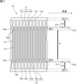
- FIG. 1 is a schematic plan view for explaining an electrode structure of an elastic wave device according to a first embodiment of the present invention.
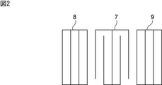
- FIG. 2 is a schematic diagram showing an electrode structure of the elastic wave device according to the first embodiment of the present invention.
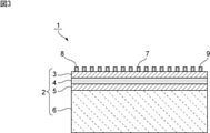
- FIG. 3 is a front sectional view of the elastic wave device according to the first embodiment of the present invention.
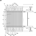
- FIG. 4 is a partially cutaway plan view showing a main part of the IDT electrode of the elastic wave device according to the first embodiment of the present invention.
- 5 (a) and 5 (b) are partial plan views showing enlarged portions indicated by arrows A and B in FIG. 1.
- FIG. 6 is a diagram showing the Q characteristics of Example 1 and Comparative Example 1.
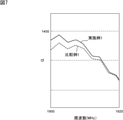
- FIG. 7 is an enlarged view showing a part of the Q characteristic diagram of FIG. FIG.
- FIG. 8 is a schematic plan view showing the electrode structure of the elastic wave device according to the second embodiment of the present invention.
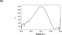
- FIG. 9 is a diagram showing the Q characteristics of the elastic wave devices of Examples 1 to 4.
- FIG. 10 is an enlarged view showing a part of FIG. 9.
- FIG. 11 is a partially cutaway plan view showing the electrode structure of the elastic wave device according to the third embodiment of the present invention.
- FIG. 12 is a front sectional view of the elastic wave device according to the fourth embodiment of the present invention.
- FIG. 13 is a front sectional view of the elastic wave device according to the fifth embodiment of the present invention.
- FIG. 3 is a front sectional view of the elastic wave device according to the first embodiment of the present invention.
- the elastic wave device 1 has a piezoelectric substrate 2.
- the piezoelectric substrate 2 has a piezoelectric film 3, a low sound velocity material layer 4, a high sound velocity material layer 5, and a support substrate 6.
- An IDT electrode 7 and reflectors 8 and 9 are provided on the piezoelectric substrate 2.
- the electrode structure of the elastic wave device 1 includes an IDT electrode 7 and reflectors 8 and 9 provided on both sides of the IDT electrode 7 in the elastic wave propagation direction. As a result, a 1-port type elastic wave resonator is configured.
- the feature of the elastic wave device 1 is the specific electrode structure of the IDT electrode 7. This electrode structure will be described in detail with reference to FIGS. 1, 4, 5 (a) and 5 (b).
- FIG. 1 is a schematic plan view showing the electrode structure of the elastic wave device 1.
- the IDT electrode 7 has first and second bus bars 11 and 12 facing each other. Details of the IDT electrode 7 are shown in FIG. 4 in a plan view with a partial notch.
- a plurality of first electrode fingers 13 are connected to the first bus bar 11.
- the first electrode finger 13 extends from the first bus bar 11 toward the second bus bar 12.
- a plurality of second electrode fingers 14 are connected to the second bus bar 12.
- the second electrode finger 14 extends from the second bus bar 12 toward the first bus bar 11.
- the region where the first electrode finger 13 and the second electrode finger 14 overlap when viewed in the elastic wave propagation direction is the crossing region K.
- the crossover region K has a central region C and first and second low sound velocity regions D1 and D2 provided on both outer sides in the direction in which the first and second electrode fingers 13 and 14 of the central region C extend.
- other regions may exist outside the first and second low sound velocity regions D1 and D2.
- the IDT electrode 7 is made of an appropriate metal or alloy.
- mass addition films 13a and 14a are provided on the first and second electrode fingers 13 and 14 as shown by hatching of diagonal lines.
- the mass addition films 13a and 14a are made of metal or a dielectric. Due to the provision of the mass addition films 13a and 14a, as shown on the right side of FIG. 4, the sound velocity V2 in the first and second low sound velocity regions D1 and D2 is lower than the sound velocity V1 in the central region C. Has been done.
- the mass addition films 13a and 14a may be laminated on the lower surface side of the first and second electrode fingers 13 and 14.
- the mass addition films 13a and 14a are laminated on the first and second electrode fingers 13 and 14, but when they are made of a dielectric film, the first and second electrode fingers 13 and 14 are formed.
- a mass addition film may be formed so as to reach the region between them.
- the first bus bar 11 is provided with a plurality of openings 11a along the elastic wave propagation direction.
- the inner bus bar portion 11b is provided on the crossing region K side of the opening 11a.
- the outer bus bar portion 11c is provided in the outer region opposite to the crossing region K of the opening 11a.
- the inner bus bar portion 11b and the outer bus bar portion 11c are connected by a plurality of connecting portions 11d.
- the connecting portion 11d extends in a direction orthogonal to the elastic wave propagation direction, and in the present embodiment, the connecting portion 11d is provided at a position where the first electrode finger 13 is extended.
- the inner bus bar portion 11b is the first inner bus bar portion in the present invention
- the outer bus bar portion 11c is the first outer bus bar portion in the present invention.
- the second bus bar 12 is similarly configured. That is, the second bus bar 12 has a plurality of openings 12a.
- An inner bus bar portion 12b is provided on the crossing region K side of the opening 12a.
- An outer bus bar portion 12c is provided in the outer region of the opening 12a opposite to the crossing region K.
- the inner bus bar portion 12b and the outer bus bar portion 12c are connected by a plurality of connecting portions 12d.
- the inner bus bar portion 12b is the second inner bus bar portion in the present invention
- the outer bus bar portion 12c is the second outer bus bar portion in the present invention.
- the sound velocities in the regions outside the first and second low sound velocity regions D1 and D2 are V10, V11, V12 and V13 shown in FIG. That is, the high sound velocity regions represented by the sound velocity V10, V11 and V12 are located outside the direction in which the first and second electrode fingers 13 and 14 of the first and second low sound velocity regions D1 and D2 extend. .. Therefore, the transverse mode ripple can be effectively confined.
- FIG. 5A is a partial plan view showing an enlarged portion of the main part of the IDT electrode 7 shown in FIG. 4, that is, the part indicated by the arrow A in FIG.
- FIG. 5B is a partial plan view showing an enlarged portion indicated by an arrow B in FIG.
- the first bus bar 11 has a wide connecting portion 11d1.
- the wide connecting portion 11d1 has a dimension along the elastic wave propagation direction, that is, a width larger than that of the remaining connecting portion 11d (FIG. 5A).
- FIG. 5B the boundary between the outer bus bar portion 11c and the wide connecting portion 11d1 is shown by a broken line X1. Further, the boundary between the wide connecting portion 11d1 and the inner bus bar portion 11b is indicated by a broken line X2.
- the width of the wide connecting portion 11d1 is larger than the width of the remaining connecting portion 11d, it is possible to reduce the electric resistance between the outer bus bar portion 11c and the inner bus bar portion 11b in the first bus bar 11. Therefore, deterioration of the Q characteristic can be suppressed.
- a pair of wide connecting portions 11d1, 11d1 are provided so as to be separated from each other in the elastic wave propagation direction of the first bus bar 11.
- wide connecting portions 12d1 and 12d1 are provided so as to be separated in the elastic wave propagation direction. Since the plurality of wide connecting portions 11d1, 11d1 or the wide connecting portions 12d1, 12d1 are provided, the electrical connection resistance between the outer bus bar portions 11c and 12c and the inner bus bar portions 11b and 12b can be further reduced. Therefore, the deterioration of the Q characteristic can be suppressed more effectively.
- the wide connecting portion may be provided at at least one place in at least one of the first bus bar 11 and the second bus bar 12. Therefore, the wide connecting portion 11d1 may be provided only on the first bus bar 11.
- both the first bus bar 11 and the second bus bar 12 are provided with a wide connecting portion. Further, it is more preferable that a plurality of wide connecting portions 11d1, 11d1, 12d1, 12d1 are provided in both the first and second bus bars 11 and 12, as in the present embodiment.
- a pair of wide connecting portions 11d1, 11d1 are provided at both ends of the first bus bar 11 in the elastic wave propagation direction. Also in the second bus bar 12, a pair of wide connecting portions 12d1, 12d1 are provided at both ends in the elastic wave propagation direction. Therefore, the leakage of energy of elastic waves is reduced, and in the present embodiment, the deterioration of the Q value is less likely to occur. Therefore, it is more preferable that at least one of the first and second bus bars 11 and 12 is provided with wide connecting portions 11d1, 11d1 or wide connecting portions 12d1, 12d1 at both ends in the elastic wave propagation direction.
- the width of the wide connecting portions 11d1, 12d1 may be larger than the remaining connecting portions 11d and 12d, but is preferably 10 ⁇ m or more and 30 ⁇ m or less. Further, when the wavelength determined by the electrode finger pitches of the first and second electrode fingers 13 and 14 is ⁇ , the width of the wide connecting portions 11d1, 12d1 is preferably 1 ⁇ or more and 10 ⁇ or less. If it is 1 ⁇ or more, the decrease in the Q value can be suppressed more effectively. Further, when it is 10 ⁇ or less, the transverse mode ripple can be suppressed more effectively.
- both ends of a plurality of electrode fingers are short-circuited by a pair of bus bars. That is, the reflectors 8 and 9 are grating type reflectors, and the structure thereof is not particularly limited.
- the piezoelectric substrate 2 has a structure in which a high sound velocity material layer 5, a low sound velocity material layer 4, and a piezoelectric film 3 are laminated in this order on a support substrate 6.
- the support substrate 6 is made of an appropriate semiconductor or dielectric material such as Si or alumina.
- the piezoelectric film 3 a piezoelectric single crystal such as LiTaO 3 can be used.
- the low sound velocity material layer 4 is made of a low sound velocity material.
- the low sound velocity material means a material in which the sound velocity of the propagating bulk wave is lower than the sound velocity of the bulk wave propagating in the piezoelectric film 3. Examples of such a low sound velocity material include glass, silicon oxide, silicon nitride, lithium oxide, tantalum pentoxide, and a material whose main component is a compound obtained by adding fluorine, carbon, or boron to silicon oxide. can.
- the high sound velocity material layer 5 is made of a high sound velocity material in which the sound velocity of the propagating bulk wave is higher than the sound velocity of the elastic wave propagating in the piezoelectric film 3.
- Such high-frequency materials include silicon, aluminum oxide, silicon carbide, silicon oxynitride, sapphire, lithium tantalate, lithium niobate, crystal, alumina, zirconia, cozilite, mulite, steatite, forsterite, magnesia, etc.
- Examples thereof include a medium containing the above-mentioned material as a main component, such as a DLC (diamond-like carbon) film or diamond.
- the low sound velocity material layer 4 may be omitted.
- the piezoelectric substrate 2 Since the piezoelectric substrate 2 has the laminated structure, the energy of elastic waves can be effectively confined in the piezoelectric film 3.
- Example 1 The design parameters of Example 1 are as follows.
- Width of wide connecting portion 11d1, 12d1 100.46 ⁇ .
- the width of the outer bus bar portions 11c and 12c (dimensions in the extending direction of the first and second electrode fingers 13 and 14) 5.66 ⁇ .
- Logarithm of electrode fingers 100.
- Piezoelectric film 3 LiTaO 3 with a thickness of 0.19 ⁇ .
- Low sound velocity material layer 4 SiN, thickness 0.14 ⁇ .
- Hypersonic material layer 5 SiO 2 , thickness 0.14 ⁇ .
- Support substrate 6 Si.
- Comparative Example 1 the wide connecting portions 11d1, 11d1, 12d1, 12d1 were not provided, and the remaining connecting portions 11d and 12d were provided in the same manner as the portions.
- Other configurations of Comparative Example 1 were the same as those of Example 1.
- FIG. 6 is a diagram showing the Q characteristics of Example 1 as an example of the elastic wave device 1 of the first embodiment and Comparative Example 1.
- the solid line shows the result of Example 1, and the broken line shows the result of Comparative Example 1.
- FIG. 7 is an enlarged view showing a part of FIG. 6. As is clear from FIGS. 6 and 7, in the vicinity of 1900 MHz where the Q value is the highest, the Q value can be effectively increased according to Example 1 as compared with Comparative Example 1. That is, it can be seen that the deterioration of the Q characteristic is less likely to occur as compared with Comparative Example 1.
- FIG. 8 is a schematic plan view showing the electrode structure of the elastic wave device according to the second embodiment of the present invention.
- the elastic wave device 21 the positions of the wide connecting portions 11d1 and 12d1 along the elastic wave propagation direction of the IDT electrode 7 were changed.
- the elastic wave device 21 is the same as the elastic wave device 1.
- the wide connecting portions 11d1 and 11d1 are located inside the first bus bar 11 in the elastic wave propagation direction from both ends in the elastic wave propagation direction. More specifically, where L is the distance between one end of the first bus bar 11 in the elastic wave propagation direction and the wide connecting portion 11d1, L> 0.
- the wide connecting portion 12d1 in the second bus bar 12 was also arranged in the same manner.
- the wide connecting portions 11d1 and 12d1 are located inside the ends of the first and second bus bars 11 and 12 in the elastic wave propagation direction as described above. As described above, the wide connecting portions 11d1, 12d1 may be located inside the ends of the first and second bus bars 11 and 12 in the elastic wave propagation direction. Even in that case, deterioration of the Q characteristic can be suppressed by lowering the electric resistance.
- the elastic wave device of Example 1 and the elastic wave device of Examples 2 to 4 below were configured with the same design parameters except for the distance L.
- FIG. 9 shows the Q characteristics of the elastic wave devices of Examples 1 and 2 to 4. Further, a part of FIG. 9 is enlarged and shown in FIG. In FIG. 10, the solid line shows the result of Example 1, the broken line shows the result of Example 2, the one-dot chain line shows the result of Example 3, and the two-dot chain line shows the result of Example 4.
- Example 1 is less likely to cause deterioration of Q characteristics than Examples 2 to 4, and is more preferable.
- FIG. 11 is a partially cutaway plan view for explaining the electrode structure of the elastic wave device according to the third embodiment of the present invention.
- the first electrode finger 13 and the second electrode finger 14 have wide portions 13b and 14b.
- the region where the wide portions 13b and 14b are provided is defined as a low sound velocity region.
- the elastic wave device 31 of the third embodiment is configured in the same manner as the elastic wave device 1 of the first embodiment.
- the first and second low sound velocity regions are not the mass-added film, but a part of the first and second electrode fingers 13 and 14 are the wide portions 13b and 14b. It may be configured.
- FIG. 12 is a front sectional view of the elastic wave device according to the fourth embodiment of the present invention.
- the piezoelectric substrate 2 has a hypersonic support substrate 5A.
- the hypersonic support substrate 5A is made of the above-mentioned hypersonic material.
- the hypersonic support substrate 5A is used instead of the support substrate 6 shown in FIG. Therefore, the hypersonic material layer 5 shown in FIG. 3 can be omitted.
- FIG. 13 is a front sectional view of the elastic wave device according to the fifth embodiment of the present invention.
- the piezoelectric substrate 52 is used as the piezoelectric substrate.
- the piezoelectric substrate 52 is made of a single crystal such as LiNbO 3 or LiTaO 3.
- the piezoelectric substrate may be composed of a single piezoelectric single crystal substrate in this way.
Landscapes
- Physics & Mathematics (AREA)
- Acoustics & Sound (AREA)
- Surface Acoustic Wave Elements And Circuit Networks Thereof (AREA)
Abstract
Q特性の劣化が生じ難い、弾性波装置を提供する。 圧電性基板2と、圧電性基板2上に設けられたIDT電極7とを備え、IDT電極7が、第1,第2の電極指が弾性波伝搬方向に沿って重なり合っている交叉領域を有し、交叉領域が、中央領域と、中央領域の第1,第2の電極指の延びる方向両外側の第1,第2の低音速領域とを有し、第1,第2のバスバー11,12が、複数の開口11a,12aを有し、開口11a,12aの一方側に位置している内側バスバー部11b,12bと、他方側に位置している外側バスバー部11c,12cとが、複数の連結部11d,12dにより連結されており、複数の連結部11d,12dのうち少なくとも1つが、残りの連結部11d,12dよりも、幅が大きい、広幅連結部11d1,12d1である、弾性波装置1。
Description
本発明は、第1,第2のバスバーを有し、第1,第2のバスバー内に複数の開口が設けられている、弾性波装置に関する。
従来、横モードリップルを抑圧するために、ピストンモードを利用した弾性波装置が知られている。例えば下記の特許文献1では、IDT電極の交叉領域において、中央領域と、中央領域の両側に設けられた低音速領域とが設けられている。そして、バスバーに、伝搬方向に沿って複数の開口が設けられている。バスバーにおける開口の交叉領域側の部分が内側バスバー部とされており、交叉領域とは反対の外側部分が外側バスバー部とされている。内側バスバー部と外側バスバー部とが、複数の細い連結部により接続されている。それによって、開口が設けられている部分が内側バスバー部と共に、高音速領域とされている。
特許文献1に記載の弾性波装置では、内側バスバー部と外側バスバー部とが、複数の細い連結部により接続されていた。そのため、Q特性が劣化するという問題があった。
本発明の目的は、Q特性の劣化が生じ難い、弾性波装置を提供することにある。
本発明に係る弾性波装置は、圧電性基板と、前記圧電性基板上に設けられたIDT電極とを備え、前記IDT電極が、対向し合っている第1及び第2のバスバーと、前記第1のバスバーから前記第2のバスバー側に延ばされた複数本の第1の電極指と、前記第2のバスバーから前記第1のバスバー側に延ばされた複数本の第2の電極指とを有し、前記第1の電極指と前記第2の電極指とが弾性波伝搬方向において重なり合っている交叉領域が、前記第1及び前記第2の電極指の延びる方向中央に位置している中央領域と、前記中央領域の前記第1及び前記第2の電極指の延びる方向両外側に配置された第1及び第2の低音速領域とを有し、前記第1及び前記第2の低音速領域の音速が前記中央領域の音速よりも低くされており、前記第1及び前記第2のバスバーが、弾性波伝搬方向に沿って設けられた複数の開口を有し、前記第1及び前記第2のバスバーにおける前記複数の開口の前記交叉領域側の部分が、それぞれ、第1及び第2の内側バスバー部とされており、前記複数の開口の前記交叉領域とは反対側の部分がそれぞれ第1及び第2の外側バスバー部とされており、前記第1及び前記第2の内側バスバー部と、前記第1及び前記第2の外側バスバー部とが、複数の連結部により連結されており、前記複数の連結部のうち少なくとも1つが、残りの前記連結部よりも弾性波伝搬方向に沿う寸法が大きい、広幅連結部である。
本発明によれば、Q特性の劣化が生じ難い、弾性波装置を提供することができる。
以下、図面を参照しつつ、本発明の具体的な実施形態を説明することにより、本発明を明らかにする。
なお、本明細書に記載の各実施形態は、例示的なものであり、異なる実施形態間において、構成の部分的な置換または組み合わせが可能であることを指摘しておく。
図3は、本発明の第1の実施形態に係る弾性波装置の正面断面図である。弾性波装置1は、圧電性基板2を有する。圧電性基板2は、圧電膜3、低音速材料層4、高音速材料層5及び支持基板6を有する。圧電性基板2上に、IDT電極7と、反射器8,9とが設けられている。図2に模式図で示すように、弾性波装置1の電極構造は、IDT電極7と、IDT電極7の弾性波伝搬方向両側に設けられた反射器8,9とを有する。それによって、1ポート型の弾性波共振子が構成されている。
弾性波装置1の特徴は、IDT電極7の具体的な電極構造にある。この電極構造を、図1、図4、図5(a)及び図5(b)を参照して詳細に説明する。
図1は、弾性波装置1の電極構造を示す略図的平面図である。IDT電極7は、対向し合っている第1,第2のバスバー11,12を有する。IDT電極7の詳細を図4に部分切欠き平面図で示す。第1のバスバー11に、複数本の第1の電極指13が接続されている。第1の電極指13は、第1のバスバー11から第2のバスバー12側に向かって延びている。第2のバスバー12に、複数本の第2の電極指14が接続されている。第2の電極指14は、第2のバスバー12から第1のバスバー11側に向かって延びている。第1の電極指13と第2の電極指14とを、弾性波伝搬方向にみたときに重なっている領域が交叉領域Kである。交叉領域Kは、中央領域Cと、中央領域Cの第1,第2の電極指13,14が延びる方向両外側に設けられた第1,第2の低音速領域D1,D2とを有する。なお、第1,第2の低音速領域D1,D2の外側に、他の領域が存在していてもよい。
IDT電極7は、適宜の金属もしくは合金からなる。第1,第2の低音速領域D1,D2において、斜線のハッチングで示すように、第1,第2の電極指13,14上に、質量付加膜13a,14aが設けられている。質量付加膜13a,14aは、金属または誘電体からなる。質量付加膜13a,14aが設けられていることにより、図4の右側において示すように、中央領域Cにおける音速V1に比べて、第1,第2の低音速領域D1,D2の音速V2が低められている。
なお、質量付加膜13a,14aは、第1,第2の電極指13,14の下面側に積層されていてもよい。
なお、図4では、質量付加膜13a,14aは、第1,第2の電極指13,14に積層されていたが、誘電体膜からなる場合、第1,第2の電極指13,14間の領域に至るように質量付加膜が形成されていてもよい。
第1のバスバー11には、弾性波伝搬方向に沿って複数の開口11aが設けられている。第1のバスバー11では、開口11aの交叉領域K側に内側バスバー部11bが設けられている。開口11aの交叉領域Kとは反対の外側の領域に外側バスバー部11cが設けられている。第1のバスバー11では、内側バスバー部11bと、外側バスバー部11cとが、複数の連結部11dにより接続されている。特に限定されないが、連結部11dは、弾性波伝搬方向と直交する方向に延びており、本実施形態では、第1の電極指13を延長した位置に設けられている。なお、内側バスバー部11bは本発明における第1の内側バスバー部であり、外側バスバー部11cは本発明における第1の外側バスバー部である。
第2のバスバー12も同様に構成されている。すなわち、第2のバスバー12は、複数の開口12aを有する。そして、開口12aの交叉領域K側に、内側バスバー部12bが設けられている。開口12aの交叉領域Kとは反対の外側の領域には、外側バスバー部12cが設けられている。内側バスバー部12bと、外側バスバー部12cとが、複数の連結部12dにより連結されている。なお、内側バスバー部12bは本発明における第2の内側バスバー部であり、外側バスバー部12cは本発明における第2の外側バスバー部である。
IDT電極7は上記のような構造を有するため、第1,第2の低音速領域D1,D2の外側の領域における音速は、図4に示すV10、V11、V12及びV13となる。すなわち、第1,第2の低音速領域D1,D2の第1,第2の電極指13,14が延びる方向外側に、音速V10,V11及びV12で示される高音速領域が位置することになる。そのため、横モードリップルを効果的に閉じ込めることができる。
図5(a)は、図4に示したIDT電極7の主要部、すなわち図1の矢印Aで示した部分を拡大して示す部分平面図である。図5(b)は、図1において矢印Bで示した部分を拡大して示す部分平面図である。
第1のバスバー11は、広幅連結部11d1を有する。広幅連結部11d1は、弾性波伝搬方向に沿う寸法、すなわち幅が残りの連結部11d(図5(a))より大きくされている。図5(b)では、外側バスバー部11cと、広幅連結部11d1との境界を破線X1で示す。また、広幅連結部11d1と内側バスバー部11bとの境界を破線X2で示す。
この広幅連結部11d1の幅が、残りの連結部11dの幅よりも大きいため、第1のバスバー11において、外側バスバー部11cと内側バスバー部11bとの間の電気抵抗を下げることができる。よって、Q特性の劣化を抑制することができる。
特に、図1に示すように、本実施形態では、一対の広幅連結部11d1,11d1が第1のバスバー11の弾性波伝搬方向に隔てられて設けられている。第2のバスバー12においても、広幅連結部12d1,12d1が弾性波伝搬方向において隔てられて設けられている。複数の広幅連結部11d1,11d1または広幅連結部12d1,12d1が設けられているため、上記外側バスバー部11c,12cと内側バスバー部11b,12bとの電気的接続抵抗をより小さくすることができる。従って、Q特性の劣化を、より効果的に抑制することができる。
なお、本発明において、広幅連結部は、第1のバスバー11及び第2のバスバー12の少なくとも一方において、少なくとも1箇所に設けられておればよい。従って、第1のバスバー11に広幅連結部11d1が設けられているだけでもよい。
第1のバスバー11及び第2のバスバー12の双方において、広幅連結部が設けられていることが好ましい。また、本実施形態のように、複数の広幅連結部11d1,11d1,12d1,12d1が、第1,第2のバスバー11,12の双方において設けられていることがより好ましい。
図1に示すように、一対の広幅連結部11d1,11d1は、第1のバスバー11の弾性波伝搬方向両端に設けられている。第2のバスバー12においても、一対の広幅連結部12d1,12d1が弾性波伝搬方向両端に設けられている。そのため、弾性波のエネルギーの漏洩が小さくなり、本実施形態では、Q値の劣化がさらに一層生じ難い。従って、さらに好ましくは、第1,第2のバスバー11,12の少なくとも一方において、弾性波伝搬方向両端に広幅連結部11d1,11d1または広幅連結部12d1,12d1が設けられていることが望ましい。
上記広幅連結部11d1,12d1の幅は、残りの連結部11d,12dよりも大きければよいが、好ましくは、10μm以上、30μm以下である。また、第1,第2の電極指13,14の電極指ピッチで定まる波長をλとしたとき、上記広幅連結部11d1,12d1の幅は、1λ以上、10λ以下であることが好ましい。1λ以上であれば、上記Q値の低下をより効果的に抑制することができる。また、10λ以下であれば、横モードリップルをより効果的に抑制することができる。
反射器8,9では、複数本の電極指の両端が一対のバスバーで短絡されている。すなわち、反射器8,9はグレーティング型反射器であり、その構造は特に限定されない。
図3に示すように、圧電性基板2は、支持基板6上に、高音速材料層5、低音速材料層4及び圧電膜3をこの順序で積層した構造を有する。支持基板6は、Siやアルミナなどの適宜の半導体もしくは誘電体材料からなる。
圧電膜3としては、LiTaO3などの圧電単結晶を用いることができる。低音速材料層4は、低音速材料からなる。低音速材料とは、伝搬するバルク波の音速が、圧電膜3を伝搬するバルク波の音速よりも低い材料をいう。このような低音速材料としては、ガラス、酸化ケイ素、酸窒化ケイ素、酸化リチウム、五酸化タンタル、または、酸化ケイ素にフッ素、炭素やホウ素を加えた化合物を主成分とする材料などを挙げることができる。
高音速材料層5は、伝搬するバルク波の音速が、圧電膜3を伝搬する弾性波の音速よりも高い高音速材料からなる。このような高音速材料としては、シリコン、酸化アルミニウム、炭化ケイ素、酸窒化ケイ素、サファイア、タンタル酸リチウム、ニオブ酸リチウム、水晶、アルミナ、ジルコニア、コージライト、ムライト、ステアタイト、フォルステライト、マグネシア、DLC(ダイヤモンドライクカーボン)膜またはダイヤモンドなど、上記材料を主成分とする媒質などを挙げることができる。
なお、低音速材料層4は省略されてもよい。
上記圧電性基板2では、上記積層構造を有するため、圧電膜3に弾性波のエネルギーを効果的に閉じ込めることができる。
次に、第1の実施形態の実施例1及び比較例1のQ特性を示すことにより、本実施形態の効果を明らかにする。
実施例1の設計パラメータは以下の通り。
IDT電極7及び反射器8,9の材料:Al。
電極指ピッチで定まる波長λ=2.12μm。電極膜厚=0.047λ。
交叉領域Kの寸法=23.58λ。中央領域Cの長さ=21.77λ。第1,第2の低音速領域D1,D2の長さ=0.90λ。
内側バスバー部11b,12bの幅(第1,第2の電極指13,14の延びる方向の寸法)=0.20λ。開口11a,12aの弾性波伝搬方向に沿う寸法=2.00λ。第1,第2の電極指13,14の延びる方向の寸法=0.43λ。連結部11d,12dの幅=1.13λ。広幅連結部11d1,12d1の幅=100.46λ。
外側バスバー部11c,12cの幅(第1,第2の電極指13,14の延びる方向の寸法)=5.66λ。
電極指の対数=100。
圧電膜3=0.19λの厚みのLiTaO3。
低音速材料層4:SiN、厚み0.14λ。
高音速材料層5:SiO2、厚み0.14λ。
支持基板6:Si。
電極指ピッチで定まる波長λ=2.12μm。電極膜厚=0.047λ。
交叉領域Kの寸法=23.58λ。中央領域Cの長さ=21.77λ。第1,第2の低音速領域D1,D2の長さ=0.90λ。
内側バスバー部11b,12bの幅(第1,第2の電極指13,14の延びる方向の寸法)=0.20λ。開口11a,12aの弾性波伝搬方向に沿う寸法=2.00λ。第1,第2の電極指13,14の延びる方向の寸法=0.43λ。連結部11d,12dの幅=1.13λ。広幅連結部11d1,12d1の幅=100.46λ。
外側バスバー部11c,12cの幅(第1,第2の電極指13,14の延びる方向の寸法)=5.66λ。
電極指の対数=100。
圧電膜3=0.19λの厚みのLiTaO3。
低音速材料層4:SiN、厚み0.14λ。
高音速材料層5:SiO2、厚み0.14λ。
支持基板6:Si。
比較例1では、上記広幅連結部11d1,11d1,12d1,12d1を設けずに、残りの連結部11d,12dが設けられている部分と同様に構成した。その他の構成は、比較例1は実施例1と同様とした。
図6は、第1の実施形態の弾性波装置1の実施例としての実施例1と、比較例1のQ特性を示す図である。実線が実施例1の結果を示し、破線が比較例1の結果を示す。図7は、図6の一部を拡大して示す図である。図6及び図7から明らかなように、Q値が最も高い1900MHz付近において、比較例1に比べて実施例1によれば、Q値を効果的に高めることができる。すなわち、比較例1に比べて、Q特性の劣化の生じ難いことがわかる。
図8は、本発明の第2の実施形態に係る弾性波装置の電極構造を示す略図的平面図である。弾性波装置21では、IDT電極7において、広幅連結部11d1,12d1の弾性波伝搬方向に沿う位置を変更した。その他の構成は、弾性波装置21は弾性波装置1と同様である。
図8に示すように、広幅連結部11d1,11d1は、第1のバスバー11の弾性波伝搬方向両端よりも弾性波伝搬方向において内側に位置している。より詳細には、第1のバスバー11の弾性波伝搬方向一端と、広幅連結部11d1との間の距離をLとすると、L>0である。第2のバスバー12における広幅連結部12d1も同様に配置した。
弾性波装置21では、広幅連結部11d1,12d1が上記のように、弾性波伝搬方向において、第1,第2のバスバー11,12の端部よりも内側に位置している。このように、広幅連結部11d1,12d1は、第1,第2のバスバー11,12の端部よりも弾性波伝搬方向において内側に位置していてもよい。その場合においても、電気抵抗を低めることにより、Q特性の劣化を抑制することができる。
上記実施例1の弾性波装置と、距離L以外は同様の設計パラメータで、以下の実施例2~4の弾性波装置を構成した。
実施例2:L=10μm=4.7λ。
実施例3:L=20μm=9.4λ。
実施例4:L=30μm=14.1λ。
実施例3:L=20μm=9.4λ。
実施例4:L=30μm=14.1λ。
実施例1及び実施例2~4の弾性波装置のQ特性を図9に示す。また、図9の一部を図10に拡大して示す。図10において、実線が実施例1、破線が実施例2、一点鎖線が実施例3、二点鎖線が実施例4の結果を示す。図10から明らかなように、実施例2~4に比べて実施例1の方がQ特性の劣化が生じ難く、より好ましいことがわかる。また、実施例2~4から、上記Lが小さい方が、Q特性の劣化を抑制し得ることがわかる。よって、より好ましくは、L=20μm未満、さらに好ましくは、9.4λ未満である。
図11は、本発明の第3の実施形態に係る弾性波装置の電極構造を説明するための部分切欠き平面図である。第3の実施形態では、第1の電極指13及び第2の電極指14が、太幅部13b,14bを有する。この太幅部13b,14bが設けられている領域が低音速領域とされている。その他の構成は、第3の実施形態の弾性波装置31は、第1の実施形態の弾性波装置1と同様に構成されている。このように、本発明では、第1,第2の低音速領域を、質量付加膜ではなく、第1,第2の電極指13,14の一部を太幅部13b,14bとすることにより構成してもよい。
図12は、本発明の第4の実施形態に係る弾性波装置の正面断面図である。弾性波装置41では、圧電性基板2が、高音速支持基板5Aを有する。高音速支持基板5Aは、前述した高音速材料からなる。この場合、図3に示した支持基板6に代えて高音速支持基板5Aが用いられている。従って、図3に示した高音速材料層5を省略することができる。
図13は、本発明の第5の実施形態に係る弾性波装置の正面断面図である。弾性波装置51では、圧電性基板として、圧電基板52が用いられている。圧電基板52は、LiNbO3やLiTaO3などの単結晶からなる。本発明においては、圧電性基板は、このように単一の圧電単結晶基板からなるものであってもよい。
1…弾性波装置
2…圧電性基板
3…圧電膜
4…低音速材料層
5…高音速材料層
5A…高音速支持基板
6…支持基板
7…IDT電極
8,9…反射器
11,12…第1,第2のバスバー
11a,12a…開口
11b,12b…内側バスバー部
11c,12c…外側バスバー部
11d,12d…連結部
11d1,12d1…広幅連結部
13,14…第1,第2の電極指
13a,14a…質量付加膜
13b,14b…太幅部
21,31,41,51…弾性波装置
52…圧電基板
2…圧電性基板
3…圧電膜
4…低音速材料層
5…高音速材料層
5A…高音速支持基板
6…支持基板
7…IDT電極
8,9…反射器
11,12…第1,第2のバスバー
11a,12a…開口
11b,12b…内側バスバー部
11c,12c…外側バスバー部
11d,12d…連結部
11d1,12d1…広幅連結部
13,14…第1,第2の電極指
13a,14a…質量付加膜
13b,14b…太幅部
21,31,41,51…弾性波装置
52…圧電基板
Claims (11)
- 圧電性基板と、
前記圧電性基板上に設けられたIDT電極とを備え、
前記IDT電極が、対向し合っている第1及び第2のバスバーと、前記第1のバスバーから前記第2のバスバー側に延ばされた複数本の第1の電極指と、前記第2のバスバーから前記第1のバスバー側に延ばされた複数本の第2の電極指とを有し、前記第1の電極指と前記第2の電極指とが弾性波伝搬方向において重なり合っている交叉領域が、前記第1及び前記第2の電極指の延びる方向中央に位置している中央領域と、前記中央領域の前記第1及び前記第2の電極指の延びる方向両外側に配置された第1及び第2の低音速領域とを有し、前記第1及び前記第2の低音速領域の音速が前記中央領域の音速よりも低くされており、
前記第1及び前記第2のバスバーが、弾性波伝搬方向に沿って設けられた複数の開口を有し、前記第1及び前記第2のバスバーにおける前記複数の開口の前記交叉領域側の部分が、それぞれ、第1及び第2の内側バスバー部とされており、前記複数の開口の前記交叉領域とは反対側の部分がそれぞれ第1及び第2の外側バスバー部とされており、前記第1及び前記第2の内側バスバー部と、前記第1及び前記第2の外側バスバー部とが、複数の連結部により連結されており、
前記複数の連結部のうち少なくとも1つが、残りの前記連結部よりも弾性波伝搬方向に沿う寸法が大きい、広幅連結部である、弾性波装置。 - 前記広幅連結部が、前記第1のバスバー及び前記第2のバスバーにおいてそれぞれ複数設けられている、請求項1に記載の弾性波装置。
- 前記第1のバスバー及び前記第2のバスバーの少なくとも一方において、一対の前記広幅連結部が設けられている、請求項2に記載の弾性波装置。
- 前記一対の広幅連結部が、前記第1及び前記第2のバスバーの少なくとも一方において、弾性波伝搬方向両端に位置している、請求項3に記載の弾性波装置。
- 前記広幅連結部の弾性波伝搬方向に沿う寸法が、前記IDT電極の前記第1及び前記第2の電極指の電極指ピッチで定まる波長をλとしたときに、1λ以上、10λ以下の範囲にある、請求項1~4のいずれか1項に記載の弾性波装置。
- 前記第1及び第2の低音速領域において、前記第1の電極指及び前記第2の電極指に積層された質量付加膜が設けられている、請求項1~5のいずれか1項に記載の弾性波装置。
- 前記第1及び第2の低音速領域において、前記第1の電極指及び前記第2の電極指の幅が、前記中央領域における前記第1の電極指及び前記第2の電極指の幅よりも大きくされている、請求項1~5のいずれか1項に記載の弾性波装置。
- 前記圧電性基板が、圧電膜と、伝搬するバルク波の音速が前記圧電膜を伝搬する弾性波の音速よりも高速である高音速材料からなる高音速材料層とを有する、請求項1~7のいずれか1項に記載の弾性波装置。
- 前記高音速材料層と、前記圧電膜との間に積層されており、伝搬するバルク波の音速が前記圧電膜を伝搬するバルク波の音速よりも低い低音速材料からなる低音速材料層をさらに備える、請求項8に記載の弾性波装置。
- 前記高音速材料層が、前記高音速材料からなる高音速支持基板である、請求項7または8に記載の弾性波装置。
- 前記圧電性基板が圧電単結晶からなる圧電基板である、請求項1~7のいずれか1項に記載の弾性波装置。
Priority Applications (2)
| Application Number | Priority Date | Filing Date | Title |
|---|---|---|---|
| CN202180048532.0A CN115777176B (zh) | 2020-07-17 | 2021-06-22 | 弹性波装置 |
| US18/092,968 US20230143523A1 (en) | 2020-07-17 | 2023-01-04 | Acoustic wave device |
Applications Claiming Priority (2)
| Application Number | Priority Date | Filing Date | Title |
|---|---|---|---|
| JP2020-122999 | 2020-07-17 | ||
| JP2020122999 | 2020-07-17 |
Related Child Applications (1)
| Application Number | Title | Priority Date | Filing Date |
|---|---|---|---|
| US18/092,968 Continuation US20230143523A1 (en) | 2020-07-17 | 2023-01-04 | Acoustic wave device |
Publications (1)
| Publication Number | Publication Date |
|---|---|
| WO2022014276A1 true WO2022014276A1 (ja) | 2022-01-20 |
Family
ID=79555266
Family Applications (1)
| Application Number | Title | Priority Date | Filing Date |
|---|---|---|---|
| PCT/JP2021/023629 Ceased WO2022014276A1 (ja) | 2020-07-17 | 2021-06-22 | 弾性波装置 |
Country Status (3)
| Country | Link |
|---|---|
| US (1) | US20230143523A1 (ja) |
| CN (1) | CN115777176B (ja) |
| WO (1) | WO2022014276A1 (ja) |
Families Citing this family (1)
| Publication number | Priority date | Publication date | Assignee | Title |
|---|---|---|---|---|
| CN117526888B (zh) * | 2023-10-07 | 2024-06-21 | 锐石创芯(重庆)科技有限公司 | 弹性波装置及射频前端模组 |
Citations (4)
| Publication number | Priority date | Publication date | Assignee | Title |
|---|---|---|---|---|
| JP2008103954A (ja) * | 2006-10-18 | 2008-05-01 | Epson Toyocom Corp | 弾性表面波素子片 |
| JP2015056746A (ja) * | 2013-09-11 | 2015-03-23 | 株式会社村田製作所 | 弾性波装置 |
| JP2019080093A (ja) * | 2017-10-20 | 2019-05-23 | 株式会社村田製作所 | 弾性波装置 |
| WO2019123812A1 (ja) * | 2017-12-19 | 2019-06-27 | 株式会社村田製作所 | 弾性波装置 |
Family Cites Families (5)
| Publication number | Priority date | Publication date | Assignee | Title |
|---|---|---|---|---|
| JP6179594B2 (ja) * | 2013-05-29 | 2017-08-16 | 株式会社村田製作所 | 弾性波装置 |
| JP5861809B1 (ja) * | 2014-05-26 | 2016-02-16 | 株式会社村田製作所 | 弾性波装置 |
| WO2016084526A1 (ja) * | 2014-11-28 | 2016-06-02 | 株式会社村田製作所 | 弾性波装置 |
| CN110178307B (zh) * | 2017-01-17 | 2023-02-28 | 株式会社村田制作所 | 弹性波装置、高频前端电路以及通信装置 |
| WO2019003909A1 (ja) * | 2017-06-26 | 2019-01-03 | 株式会社村田製作所 | 弾性波装置及び複合フィルタ装置 |
-
2021
- 2021-06-22 CN CN202180048532.0A patent/CN115777176B/zh active Active
- 2021-06-22 WO PCT/JP2021/023629 patent/WO2022014276A1/ja not_active Ceased
-
2023
- 2023-01-04 US US18/092,968 patent/US20230143523A1/en active Pending
Patent Citations (4)
| Publication number | Priority date | Publication date | Assignee | Title |
|---|---|---|---|---|
| JP2008103954A (ja) * | 2006-10-18 | 2008-05-01 | Epson Toyocom Corp | 弾性表面波素子片 |
| JP2015056746A (ja) * | 2013-09-11 | 2015-03-23 | 株式会社村田製作所 | 弾性波装置 |
| JP2019080093A (ja) * | 2017-10-20 | 2019-05-23 | 株式会社村田製作所 | 弾性波装置 |
| WO2019123812A1 (ja) * | 2017-12-19 | 2019-06-27 | 株式会社村田製作所 | 弾性波装置 |
Also Published As
| Publication number | Publication date |
|---|---|
| CN115777176B (zh) | 2026-03-17 |
| CN115777176A (zh) | 2023-03-10 |
| US20230143523A1 (en) | 2023-05-11 |
Similar Documents
| Publication | Publication Date | Title |
|---|---|---|
| JP6819834B1 (ja) | 弾性波装置 | |
| US12113509B2 (en) | Acoustic wave device with IDT electrode including al metal layer and high acoustic impedance metal layer | |
| JP6954799B2 (ja) | 弾性波装置 | |
| US9035725B2 (en) | Acoustic wave device | |
| US12388412B2 (en) | Acoustic wave device | |
| WO2022202917A1 (ja) | 弾性波装置 | |
| JPWO2018003282A1 (ja) | 弾性波装置 | |
| WO2015198897A1 (ja) | 弾性波装置 | |
| WO2011007690A1 (ja) | 弾性表面波装置 | |
| WO2020261763A1 (ja) | 弾性波装置 | |
| WO2021065684A1 (ja) | 弾性波装置 | |
| US12355425B2 (en) | Acoustic wave device | |
| WO2021241364A1 (ja) | 弾性波装置 | |
| WO2018135489A1 (ja) | 弾性波装置、高周波フロントエンド回路及び通信装置 | |
| WO2020250572A1 (ja) | 弾性波装置 | |
| WO2020202960A1 (ja) | 縦結合共振子型弾性波フィルタ及びフィルタ装置 | |
| WO2020262388A1 (ja) | フィルタ装置 | |
| JP5850209B1 (ja) | 弾性波装置 | |
| WO2022131237A1 (ja) | 弾性波装置及びラダー型フィルタ | |
| WO2022071062A1 (ja) | 弾性波装置 | |
| WO2017077892A1 (ja) | 弾性波装置 | |
| WO2022014276A1 (ja) | 弾性波装置 | |
| WO2021220974A1 (ja) | 弾性波装置 | |
| WO2023048256A1 (ja) | 弾性波装置 | |
| WO2020241776A1 (ja) | 弾性波装置 |
Legal Events
| Date | Code | Title | Description |
|---|---|---|---|
| 121 | Ep: the epo has been informed by wipo that ep was designated in this application |
Ref document number: 21841578 Country of ref document: EP Kind code of ref document: A1 |
|
| NENP | Non-entry into the national phase |
Ref country code: DE |
|
| 122 | Ep: pct application non-entry in european phase |
Ref document number: 21841578 Country of ref document: EP Kind code of ref document: A1 |
|
| NENP | Non-entry into the national phase |
Ref country code: JP |