WO2022004182A1 - 電子制御装置 - Google Patents
電子制御装置 Download PDFInfo
- Publication number
- WO2022004182A1 WO2022004182A1 PCT/JP2021/019179 JP2021019179W WO2022004182A1 WO 2022004182 A1 WO2022004182 A1 WO 2022004182A1 JP 2021019179 W JP2021019179 W JP 2021019179W WO 2022004182 A1 WO2022004182 A1 WO 2022004182A1
- Authority
- WO
- WIPO (PCT)
- Prior art keywords
- substrate
- housing
- electronic control
- connector
- protrusion
- Prior art date
Links
Images


Classifications
-
- H—ELECTRICITY
- H05—ELECTRIC TECHNIQUES NOT OTHERWISE PROVIDED FOR
- H05K—PRINTED CIRCUITS; CASINGS OR CONSTRUCTIONAL DETAILS OF ELECTRIC APPARATUS; MANUFACTURE OF ASSEMBLAGES OF ELECTRICAL COMPONENTS
- H05K1/00—Printed circuits
- H05K1/02—Details
- H05K1/14—Structural association of two or more printed circuits
-
- H—ELECTRICITY
- H05—ELECTRIC TECHNIQUES NOT OTHERWISE PROVIDED FOR
- H05K—PRINTED CIRCUITS; CASINGS OR CONSTRUCTIONAL DETAILS OF ELECTRIC APPARATUS; MANUFACTURE OF ASSEMBLAGES OF ELECTRICAL COMPONENTS
- H05K9/00—Screening of apparatus or components against electric or magnetic fields
Definitions
- the present invention relates to an electronic control device.
- the BtoB connector is a connector having an insulating housing and a plurality of conductive terminals, and is suitable for high-speed communication.
- electromagnetic noise generated during high-speed communication affects each printed circuit board, so some noise countermeasures are required.
- Patent Document 1 As a noise countermeasure, for example, the technique described in Patent Document 1 is known.
- a BtoB connector is used in which each electrical board unit is housed in a board storage housing and the corresponding connectors can be fitted to each other.
- unnecessary electromagnetic noise is radiated (unnecessary) generated from elements such as cables and circuit boards in the device by covering the periphery of each electrical board unit with a board storage housing. Radiation) is suppressed.
- An object of the present invention is to provide an electronic control device capable of suppressing transmission of electromagnetic noise between substrates and suppressing transmission of electromagnetic noise generated from a connector to the substrate.
- the present application includes a plurality of means for solving the above problems, one of which is a first substrate, a second substrate electrically connected to the first substrate by a BtoB connector, and the like.
- a housing on which a first board and a second board are mounted is provided, a housing is provided between the first board and the second board, and the housing surrounds the periphery of the BtoB connector.
- FIG. 1 is a perspective view schematically showing the appearance of the electronic control device according to the first embodiment.
- FIG. 2 is an exploded perspective view of the electronic control device according to the first embodiment as viewed from above
- FIG. 3 is an exploded perspective view of the electronic control device according to the first embodiment as viewed from below.
- the electronic control unit 100 is, for example, an electronic control unit (ECU) used in an automobile.
- the electronic control device 100 includes a housing 11, a first substrate 21, a second substrate 22, a third substrate 23, a first cover 41, a second cover 42, and a fan cover 52. , Is equipped.
- the first substrate 21, the second substrate 22, and the third substrate 23 are circuit boards (printed circuit boards) having wiring patterns, respectively.
- the second substrate 22 corresponds to a motherboard, and the first substrate 21 and the third substrate 23 correspond to a daughter board, respectively.
- the side on which the first cover 41 is arranged is described as the upper side and the side on which the second cover 42 is arranged is described as the lower side when viewed from the housing 11, but the vertical direction (vertical direction). ) And the left-right direction (horizontal direction) may change depending on the orientation of the electronic control device 100 when the electronic control device 100 is mounted on the vehicle.
- the housing 11 is made of a metal material such as aluminum or an aluminum alloy. Therefore, the housing 11 has conductivity and thermal conductivity.
- a heat radiation fin 61 is formed on the housing 11.
- the heat radiation fin 61 is a plate-shaped fin formed on the upper surface side of the housing 11.
- the heat radiation fin 61 is preferably formed integrally with the housing 11.
- a peripheral wall 12 is formed on the outer peripheral portion of the housing 11.
- the peripheral wall 12 has a first peripheral wall 12a formed on the upper surface side of the housing 11 and a second peripheral wall 12b formed on the lower surface side of the housing 11.
- the first peripheral wall 12a projects upward from the upper surface of the housing 11, and the second peripheral wall 12b projects downward from the lower surface of the housing 11.
- the holes 15 and 16 are holes through which the BtoB connectors 32 and 33 are inserted in order to electrically connect the first substrate 21 and the second substrate 22 by the BtoB connectors 32 and 33 described later. That is, the holes 15 and 16 are holes for connecting the connector.
- the holes 15 and 16 are formed so as to penetrate the housing 11 in the thickness direction (vertical direction).
- a protrusion 13 and a protrusion 14 are formed on the opening edge of the hole 15.
- the protrusion 13 is formed on the first substrate 21 side, and the protrusion 14 is formed on the second substrate 22 side. That is, the protrusions 13 and 14 are formed on both the first substrate 21 side and the second substrate 22 side.
- the protrusion 13 projects from the upper surface of the housing 11 toward the first substrate 21, and the protrusion 14 projects from the lower surface of the housing 11 toward the second substrate 22.
- Each of the protrusions 13 and 14 is preferably formed integrally with the housing 11. That is, the housing 11 and the protrusions 13 and 14 have an integral structure.
- the protrusions 13 and 14 are formed in a rectangular frame shape in a plan view, and the holes 15 and 16 are also formed in a rectangular shape in a plan view along the shape of the frame shape. Further, the protrusions 13 and 14 corresponding to the holes 15 are formed around the holes 15, and the protrusions 13 and 14 corresponding to the holes 16 are also formed around the holes 16.
- the protrusions 13 and 14 corresponding to the hole 15 are formed so as to surround the circumference of the hole 15 over the entire circumference, and the protrusions 13 and 14 corresponding to the hole 16 also surround the circumference of the hole 16. It is formed so as to surround it.
- the first substrate 21 is a substrate mounted on the upper surface side of the housing 11.
- the first substrate 21 is arranged on the upper surface side of the housing 11 at a position adjacent to the heat radiation fin 61.
- two SoCs (System on Chips) 25 are mounted on the lower surface of the first substrate 21.
- the SoC 25 is an SoC for image processing.
- the SoC25 is composed of a surface mount type package.
- As an example of the surface mount type package constituting the SoC25 a BGA package can be mentioned.
- the SoC 25 is arranged so as to be in contact with the upper surface of the housing 11 via a heat radiating material (not shown). As a result, the heat generated by the SoC 25 during high-speed communication is transferred from the SoC 25 to the housing 11.
- the heat radiating material is composed of, for example, heat radiating grease.
- a connector semifield 32a and a connector semifield 33a are mounted on the lower surface of the first substrate 21.
- the connector half body 32a is a connector having a male (male) / female (female) relationship with the connector half body 32b mounted on the second board 22, and is configured to be matable with the connector half body 32b.
- the second BtoB connector 32 is composed of a connector semifield 32a and a connector semifield 32b.
- the connector half body 33a is a connector having a male / female relationship with the connector half body 33b mounted on the second board 22, and is configured to be matable with the connector half body 33b.
- the third BtoB connector 33 is composed of a connector semifield 33a and a connector semifield 33b. Further, a plurality of connectors 34 are mounted on the lower surface of the first substrate 21. Each connector 34 is a connector for communicating with the outside, and is arranged along one side of the first board 21.
- the second substrate 22 is a substrate arranged in the housing 11.
- the second substrate 22 is mounted on the lower surface side of the housing 11.
- a PCIeSW (PCI Express Switch) 24 is mounted on the upper surface of the second substrate 22.
- the PCIeSW24 is composed of a surface mount type package.
- An example of a surface mount type package constituting the PCIeSW24 is a BGA (Ball Grid Array) package.
- the PCIeSW 24 is arranged so as to be in contact with the lower surface of the housing 11 via a heat radiating material (for example, heat radiating grease) (not shown). As a result, the heat generated by the PCIeSW 24 during high-speed communication is transferred from the PCIeSW 24 to the housing 11.
- the second substrate 22 is arranged so as to face the first substrate 21 in the vertical direction which is the direction perpendicular to the substrate surface.
- a connector semifield 31b, a connector semifield 32b, and a connector semifield 33b are mounted on the upper surface of the second substrate 22.
- the connector half body 31b is a connector having a male / female relationship with the connector half body 31a mounted on the third board 23, and is configured to be matable with the connector half body 31a.
- the first BtoB connector 31 is composed of a connector semifield 31a and a connector semifield 31b.
- the connector half body 32b is fitted with the connector half body 32a when assembling the electronic control device 100.
- the connector half body 33b is fitted with the connector half body 33a when assembling the electronic control device 100.
- a plurality of connectors 35 are mounted on the lower surface of the second substrate 22. Each connector 35 is a connector for communicating with the outside, and is arranged along one side of the second board 22.
- the third substrate 23 is arranged on the same plane as the second substrate 22.
- the third substrate 23 is provided on the region where the heat radiation fins 61 are formed.
- the third substrate 23 is mounted on the lower surface side of the housing 11 together with the second substrate 22.
- An accelerator SoC (hereinafter referred to as "accelerator") 26 is mounted on the upper surface of the third substrate 23.
- the accelerator 26 is composed of a surface mount type package (for example, a BGA package).
- the accelerator 26 is arranged so as to be in contact with the lower surface of the housing 11 via a heat radiating material (for example, heat radiating grease) (not shown). As a result, the heat generated by the accelerator 26 during high-speed communication is transferred from the accelerator 26 to the housing 11.
- a connector semifield 31a is mounted on the upper surface of the third substrate 23.
- the connector semifield 31a is mounted on the upper surface of the third substrate 23.
- the connector half body 31a is fitted to the above-mentioned connector half body 31b from the horizontal direction. As a result, the second board 22 and the third board 23 are horizontally connected by the first BtoB connector 31.
- the first cover 41 is a cover that covers the first substrate 21.
- the lower surface of the first cover 41 is arranged to face the upper surface of the first substrate 21, and the upper surface of the housing 11 is arranged to face the lower surface of the first substrate 21. Therefore, the first substrate 21 is arranged in the space formed by the housing 11 and the first cover 41 in the vertical direction.
- the first cover 41 is formed in a quadrangle in plan view with dimensions larger than the external dimensions of the first substrate 21 so that the entire area of the first substrate 21 can be shielded.
- the first cover 41 is made of a metal material such as an iron alloy, more specifically, a plated steel plate or the like.
- the electronic control device 100 By providing the electronic control device 100 with the first cover 41, it is possible to prevent the intrusion of dust and the like from the outside to the inside of the electronic control device 100 by the first cover 41 and suppress the occurrence of contamination. Further, by covering the first substrate 21 with the first cover 41, external contact with the first substrate 21 is blocked by the first cover 41, and the first substrate 21 is protected from trauma and the like. Can be done.
- the second cover 42 is a cover that covers the second substrate 22 and the third substrate 23.
- the upper surface of the second cover 42 is arranged to face the lower surfaces of the second substrate 22 and the third substrate 23, and the lower surface of the housing 11 is placed on the upper surfaces of the second substrate 22 and the third substrate 23. They are placed facing each other. Therefore, the second substrate 22 and the third substrate 23 are arranged in the space formed by the housing 11 and the second cover 42 in the vertical direction.
- the second cover 42 is viewed in a plan view with dimensions larger than the dimensions of the outermost peripheral portions of the second substrate 22 and the third substrate 23 so that the entire area of the second substrate 22 and the third substrate 23 can be shielded. It is formed in a quadrangle.
- the second cover 42 is made of a metal material such as an iron alloy, more specifically, a plated steel plate or the like.
- a metal material such as an iron alloy, more specifically, a plated steel plate or the like.
- the fan cover 52 is a cover provided so as to cover the heat radiation fin 61.
- the fan cover 52 is formed with three openings 52a.
- the three openings 52a are openings for ventilation and are formed corresponding to the three fans 51.
- the fan 51 is a fan for forced air cooling. The number of fans 51 can be changed as needed. Further, the fan 51 may be provided as needed, and the fan cover 52 may be provided as needed.
- the opening 52a serves as an intake port for taking in air from the outside of the electronic control device 100 to the fan 51 when the fan 51 is driven.
- the fans 51 are arranged side by side in a row on the intermediate portion 61a of the heat radiation fin 61.
- the intermediate portion 61a of the heat radiation fin 61 is formed in a groove shape having no fin structure.
- the fan cover 52 is attached to the upper surface side of the housing 11 together with the first cover 41.
- the fan cover 52 is arranged next to the first cover 41.
- the fan cover 52 is formed in a rectangular shape in a plan view with dimensions that match the size of the heat radiation fins 61.
- the fan cover 52 is made of a metal material.
- the heat generated by the accelerator 26 during high-speed communication is also conducted to the heat radiation fin 61 of the housing 11, the heat generated by the accelerator 26 is transferred to the outside of the housing 11 by air-cooling the heat radiation fin 61 by the fan 51. Can be escaped efficiently.
- the electronic control device 100 having the above configuration is assembled, for example, by the following procedure. First, the connector half body 31b mounted on the second board 22 and the connector half body 31a mounted on the third board 23 are fitted. As a result, the second substrate 22 and the third substrate 23 are horizontally connected by the first BtoB connector 31. Therefore, a large amount of data can be communicated at high speed between the second substrate 22 and the third substrate 23 through the first BtoB connector 31.
- the second substrate 22 and the third substrate 23 are attached to the lower surface side of the housing 11.
- the connector semifields 32b and 33b mounted on the second board 22 are arranged inside the corresponding holes 15 and 16, respectively.
- the second substrate 22 and the housing 11 are fastened with screws 71 (see FIG. 1).
- the second cover 42 is attached to the lower surface side of the housing 11 so as to cover the second substrate 22 and the third substrate 23.
- the gap between the second cover 42 and the connector 35 and the gap between the second cover 42 and the housing 11 are each filled with a waterproof material (not shown).
- the waterproof material prevents water from entering the inside of the electronic control device 100 from the outside, and protects the substrates 21 to 23 in the electronic control device 100.
- a fan cover 52 is attached to the upper surface side of the housing 11 so as to cover the heat radiation fins 61.
- the first substrate 21 is attached to the upper surface side of the housing 11.
- the connector semifields 32a and 33a mounted on the first board 21 are arranged inside the corresponding holes 15 and 16, respectively.
- the first board 21 and the housing 11 are fastened with screws 71 (see FIG. 1).
- the connector half body 32a is fitted to the connector half body 32b
- the connector half body 33a is fitted to the connector half body 33b.
- the first board 21 and the second board 22 are vertically connected by the second BtoB connector 32 and the third BtoB connector 33. Further, as shown in FIG.
- the connector semifields 33a and 33b constituting the third BtoB connector 33 are arranged in the space of the hole 16, and the connector semifields 33a and 33b are connected to each other in this space. ..
- the protrusions 13 and 14 formed on the housing 11 are arranged so as to surround the periphery of the third BtoB connector 33.
- the connector halves 32a and 32b constituting the second BtoB connector 32 are arranged in the space of the hole 15, and the connector halves 32a and 32b are connected to each other in this space.
- the protrusions 13 and 14 formed on the housing 11 are arranged so as to surround the periphery of the second BtoB connector 32.
- the first cover 41 is attached to the upper surface side of the housing 11 so as to cover the first substrate 21.
- the gap between the first cover 41 and the connector 34 and the gap between the first cover 41 and the housing 11 are each filled with a waterproof material (not shown).
- the reason for providing the waterproof material is as described above. This completes the assembly of the electronic control device 100.
- the assembly procedure of the electronic control device 100 is not limited to the procedure described above, and can be appropriately changed.
- the first substrate 21 is mounted on one side (upper surface side) of the housing 11, and the second substrate 22 is mounted on the other side (lower surface side) of the housing 11. ..
- a housing 11 is interposed between the first substrate 21 and the second substrate 22.
- the electromagnetic noise generated in the first substrate 21 and the electromagnetic noise generated in the second substrate 22 are shielded by the housing 11. Therefore, it is possible to suppress the electromagnetic noise generated in the first substrate 21 from being transmitted to the second substrate 22, and the electromagnetic noise generated in the second substrate 22 is transmitted to the first substrate 21. Can be suppressed.
- protrusions 13 and 14 are formed on the housing 11 so as to surround the periphery of the second BtoB connector 32 and the third BtoB connector 33. Therefore, when high-speed communication is performed between the first board 21 and the second board 22, the electromagnetic noise generated from the second BtoB connector 32 and the third BtoB connector 33 is shielded by the protrusions 13 and 14. Will be done. Therefore, it is possible to suppress the electromagnetic noise generated from the second BtoB connector 32 and the third BtoB connector 33 from being transmitted to the first substrate 21 and the second substrate 22.
- protrusions 13 are formed around the holes 15 and 16 so as to surround the holes 15 and 16 of the housing 11, and the protrusions 13 project toward the first substrate 21. .. By forming such a protrusion 13 on the housing 11, electromagnetic noise generated when a high-speed signal propagates through the second BtoB connector 32 and the third BtoB connector 33 is transmitted to the first substrate 21. Can be suppressed.
- protrusions 14 are formed around the holes 15 and 16 so as to surround the holes 15 and 16 of the housing 11, and the protrusions 14 project toward the second substrate 22. .. By forming such a protrusion 14 on the housing 11, electromagnetic noise generated when a high-speed signal propagates through the second BtoB connector 32 and the third BtoB connector 33 is transmitted to the second substrate 22. Can be suppressed.
- the first embodiment it is possible to suppress the transmission of electromagnetic noise between the first substrate 21 and the second substrate 22, and the second BtoB connector 32 and the third BtoB. It is possible to suppress the electromagnetic noise generated from the connector 33 from being transmitted to the first substrate 21 and the second substrate 22. Therefore, it is possible to suppress malfunction of the electronic control device 100 due to electromagnetic noise and provide a highly reliable electronic control device 100.
- the respective protrusions 13 and 14 are formed into an uneven shape so as to fit the shape of the third BtoB connector 33. It is good to do it.
- the inner wall surfaces 13a and 14a of the protrusions 13 and 14 facing the space of the hole 16 are formed in a stepped shape together with the inner wall surface 11a of the housing 11 facing the space of the hole 16.
- the gap between 13, 14 and the third BtoB connector 33 is narrowed. As a result, the air layer existing around the third BtoB connector 33 can be reduced, which is more preferable in terms of measures against electromagnetic noise.
- the protrusions 13 and 14 are formed in a concavo-convex shape so as to fit the shape of the second BtoB connector 32, the air layer existing around the second BtoB connector 32 can be formed. Since it can be reduced, it is more preferable in terms of measures against electromagnetic noise.
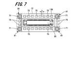
- FIG. 6 is a side sectional view showing a main part of the electronic control device according to the second embodiment
- FIG. 7 is a plan view showing a main part of the electronic control device according to the second embodiment. In FIG. 7, the notation of the first substrate 21 and the second substrate 22 is omitted.
- screw pedestals 81 are provided at the four corners of the protrusion 13, and screw pedestals 81 are also provided at the four corners of the protrusion 14. In the protrusion 13, the screw pedestal 81 protrudes more than the other parts, and in the protrusion 14, the screw pedestal 81 also protrudes more than the other parts.
- a female screw (not shown) is formed on the screw pedestal portion 81, and a screw (male screw) 71 is attached to this female screw.
- the first board 21 is attached to each protrusion 13 using four screws 71, and on the lower surface side of the housing 11, four screws 71 are attached to each protrusion 14.
- the second substrate 22 is attached using the above. In other words, the first board 21 and each of the protrusions 13 are fastened at four places with screws 71, and the second board 22 and each of the protrusions 14 are fastened at four places with screws 71. ..
- a GND pattern portion 27 is provided at a predetermined portion of the first substrate 21 that contacts the screw pedestal portion 81, and a predetermined portion of the second substrate 22 that contacts the screw pedestal portion 81. Also, a GND pattern portion 28 is provided.
- the GND pattern unit 27 is a pattern unit grounded to GND (ground) in the wiring pattern formed on the first substrate 21, and corresponds to the first GND pattern unit.
- the GND pattern portion 28 is a pattern portion grounded to the GND in the wiring pattern formed on the second substrate 22, and corresponds to the second GND pattern portion. It is preferable that the GND pattern portions 27 and 28 are formed in the widest possible range around the third BtoB connector 33, except for the signal lines included in the above wiring pattern.
- the GND pattern portion 27 of the first substrate 21 protrudes. It comes into contact with the screw pedestal portion 81 of the portion 13. As a result, the GND pattern portion 27 of the first substrate 21 is electrically connected to the housing 11 through the protrusion portion 13. Further, by providing the GND pattern portion 28 on the second substrate 22, when the second substrate 22 is fastened to the screw pedestal portion 81 by the screw 71, the GND pattern portion 28 of the second substrate 22 is formed by the protrusion portion 14. Contact the screw pedestal portion 81 of. As a result, the GND pattern portion 28 of the second substrate 22 is electrically connected to the housing 11 through the protrusion portion 14.
- a plurality of conductive members 75 are arranged on the protruding end surface 13b of the protruding portion 13, and a plurality of conductive members 76 (see FIG. 6) are arranged on the protruding end surface 14b of the protruding portion 14. ) Is placed.
- the conductive member 75 is a member that is interposed between the protruding end surface 13b of the protrusion 13 and the lower surface of the first substrate 21 to electrically connect the protrusion 13 and the first substrate 21. Corresponds to the conductive member of 1.
- the conductive member 75 is preferably composed of a gasket.
- the conductive member 76 is a member that is interposed between the protruding end surface 14b of the protrusion 14 and the upper surface of the second substrate 22 to electrically connect the protrusion 14 and the second substrate 22. Corresponds to the conductive member of 2.
- the conductive member 76 is preferably composed of a gasket. The gasket has moderate elasticity.
- the plurality of conductive members 75 are arranged at predetermined intervals along the planar shape (rectangle) of the protrusion 13.
- the gap between the conductive members 75 adjacent to each other in the longitudinal direction and the lateral direction of the rectangular protrusion 13 is L (mm)
- the wavelength of the electromagnetic noise generated from the third BtoB connector 33 is ⁇ (mm).
- the gap L satisfies L ⁇ / 2 in relation to the wavelength ⁇ . This point is the same for the plurality of conductive members 76 arranged on the protruding end surface 14b of the protrusion 14.
- the radio wave absorber 79 is composed of, for example, a radio wave absorbing sheet formed by blending a magnetic material with a flexible resin into a sheet shape, and the radio wave absorbing sheet is attached to the inner wall surfaces 13a and 14a of the protrusions 13 and 14. It is attached.
- the radio wave absorber 79 is attached from the inner wall surfaces 13a and 14a of the protrusions 13 and 14 to the inner wall surface 11a of the housing 11.
- the radio wave absorber 79 is arranged so as to surround the circumference of the third BtoB connector 33.
- the configuration described above is applied not only around the third BtoB connector 33 but also around the second BtoB connector 32.
- the first substrate 21 and the protrusion 13 are electrically connected by the conductive member 75, and the second substrate 22 and the protrusion 14 are electrically connected by the conductive member 76. Is connected to. As a result, the radiation of electromagnetic noise generated from the third BtoB connector 33 can be blocked by the conductive members 75 and 76.
- the first substrate 21 has a GND pattern portion 27 in a portion in contact with the protrusion 13
- the second substrate 22 has a GND pattern portion 28 in a portion in contact with the protrusion 14.
- the GND potential in the first substrate 21 is strengthened, and the electromagnetic noise on the first substrate 21 generated from the third BtoB connector 33 by high-speed communication can be reduced.
- the GND potential in the second substrate 22 is strengthened, and the electromagnetic noise on the second substrate 22 generated from the third BtoB connector 33 by high-speed communication can be reduced.
- the gasket is used when the conductive members 75 and 76 are gaskets. It is possible to suppress the leakage of electromagnetic noise from the gap between the two.
- the radio wave absorber 79 is arranged on the inner wall surfaces 13a and 14a of the protrusions 13 and 14, the electromagnetic noise generated from the third BtoB connector 33 is absorbed by the radio wave absorber 79. Will be done. Therefore, it is possible to suppress the radiation of electromagnetic noise generated from the third BtoB connector 33.
- the first substrate 21 and the protrusion 13 are fastened with screws 71 at four places, but the present invention is not limited to this, and the first substrate 21 and the first substrate 21 are fastened to each other.
- the protrusion 13 may be fastened with screws 71 at two places as shown in FIG. 8, or may be fastened with screws 71 at three places as shown in FIG. That is, the first substrate 21 and the protrusion 13 may be fastened with screws 71 at at least one place, more preferably at least two places. This point is the same in the relationship between the second substrate 22 and the protrusion 14.
- the screw 71 is used as the fastening member, but the present invention is not limited to this, and for example, a metal member such as a metal caulking member or a metal press-fit member is applied to the fastening member. You may.
- FIG. 10 is a plan view showing a main part of the electronic control device according to the third embodiment.
- the electronic control device according to the third embodiment has a different configuration of the conductive member as compared with the second embodiment. That is, in the second embodiment, an example in which the conductive member 75 is composed of a gasket is shown, but in the third embodiment, the conductive member 75a is an integrally molded product such as urethane foam instead of the gasket. Is configured.
- the conductive member 75a corresponds to the first conductive member.
- the conductive member 75a extends continuously in the longitudinal direction and the lateral direction of the protrusion 13 forming a rectangular shape in a plan view. Therefore, in both the longitudinal direction and the lateral direction of the protrusion 13, there is a gap between the protruding end surface 13b (see FIG. 6) of the protrusion 13 and the first substrate 21 facing the protrusion 13 with a conductive member 75a. Connected without.
- the protrusion 14 is formed by forming the conductive member with an integrally molded product such as urethane foam instead of the gasket.
- the tip surface 14b of the above and the second substrate 22 may be connected without a gap by a conductive member.
- the present invention is not limited to the above-described embodiment, and includes various modifications.
- the contents of the present invention are described in detail so as to be easy to understand, but the present invention is not necessarily limited to those including all the configurations described in the above-described embodiment.
- the protrusion 13 projecting to the upper surface side (first substrate 21 side) of the housing 11 and the protrusion projecting to the lower surface side (second substrate 22 side) of the housing 11.
- both of 14 are formed in the housing 11
- the present invention is not limited to this, and even in a configuration in which only one of the protrusions 13 and 14 is formed in the housing 11. good.
- the reason is that, as a countermeasure against radio wave noise generated from the BtoB connectors 32 and 33, a sufficient effect can be obtained even when only one of the protrusions (projection 13 or protrusion 14) is formed in the housing 11. Because there is a possibility that it will be.
- the present invention is not limited to this, and the respective protrusions 13 and 14 are not limited to this. It may be fixed to the housing 11 with a conductive adhesive, screws, or the like.
- the electronic control device used for an automobile (electronic control device for a vehicle) has been described as an example, but the electronic control device according to the present invention is used for applications other than automobiles. It doesn't matter.
Landscapes
- Engineering & Computer Science (AREA)
- Microelectronics & Electronic Packaging (AREA)
- Shielding Devices Or Components To Electric Or Magnetic Fields (AREA)
Abstract
電子制御装置は、第1の基板と、第1の基板とBtoBコネクタで電気的に接続される第2の基板と、第1の基板と第2の基板が実装される筐体と、を備え、第1の基板と第2の基板の間に筐体が設けられており、筐体は、BtoBコネクタ周辺を囲うように第1又は第2の基板側の少なくとも一方に突出した突起部が形成されている。
Description
本発明は、電子制御装置に関する。
近年、自動車に用いられる電子制御装置は、半導体デバイスなどを搭載したプリント基板を内部に有している。自動運転向けのECU(Electronic Control Unit)では、自動運転LEVELが上がるにつれて、多量のデータを高速に通信処理する必要がある。このECUは、カメラやレーダー等によって得られる画像データや信号データを演算処理し、パワーステアリングやブレーキ等を制御する他のECUに信号を送る。その場合、自動車の種類や機能差により、情報伝達量などの回路仕様あるいはSoC(System on Chip)機能要求が異なってくるため、回路基板が多様になりつつある。よって、自動車に用いられる電子制御装置のなかでも、とりわけ自動運転向けのECUでは、サイズの拡大や部品点数の増加が顕著になり、それに伴ってプリント基板や電子制御装置が大型化する傾向にある。このため、電子制御装置の更なる小型化を実現する技術が必要となっている。
電子制御装置の大型化を抑制する技術の一つとして、プリント基板を、マザーボードと複数のドーターボードとに分割し、BtoB(Board to Board)コネクタにてプリント基板間を接続する技術が考えられる。BtoBコネクタは、絶縁性のハウジングと、複数の導電端子とを有するコネクタであり、高速通信に適している。しかし、複数のプリント基板をBtoBコネクタで接続する場合は、高速通信時に発生する電磁ノイズが各々のプリント基板に影響を与えるため、何らかのノイズ対策が必要となる。
ノイズ対策として、たとえば特許文献1に記載された技術が知られている。特許文献1に記載された技術では、各電装基板ユニットを基板収納筐体に収容し、対応するコネクタ同士を嵌合できるBtoBコネクタを使用している。また、特許文献1に記載された技術では、各電装基板ユニットの周囲を基板収納筐体で覆うことにより、装置内のケーブルや回路基板などの要素から発生する、不要な電磁ノイズの放射(不要輻射)を抑制している。
特許文献1に記載された技術では、コネクタから発生する電磁ノイズの影響を抑制すべく、各電装基板ユニットの周囲を基板収納筐体で覆うことにより、基板収納筐体の外部に電磁ノイズが放射しないようにしているが、基板収納筐体の内部で回路基板自体へ伝達される電磁ノイズを抑制することについては考慮されていない。
本発明の目的は、基板間で電磁ノイズが伝達されることを抑制できると共に、コネクタから発生する電磁ノイズが基板に伝達されることを抑制できる電子制御装置を提供することにある。
上記課題を解決するために、たとえば、請求の範囲に記載された構成を採用する。
本願は、上記課題を解決する手段を複数含んでいるが、その一つを挙げるならば、第1の基板と、第1の基板とBtoBコネクタで電気的に接続される第2の基板と、第1の基板と第2の基板が実装される筐体と、を備え、第1の基板と第2の基板の間に筐体が設けられており、筐体は、BtoBコネクタ周辺を囲うように第1又は第2の基板側の少なくとも一方に突出した突起部が形成されている電子制御装置である。
本願は、上記課題を解決する手段を複数含んでいるが、その一つを挙げるならば、第1の基板と、第1の基板とBtoBコネクタで電気的に接続される第2の基板と、第1の基板と第2の基板が実装される筐体と、を備え、第1の基板と第2の基板の間に筐体が設けられており、筐体は、BtoBコネクタ周辺を囲うように第1又は第2の基板側の少なくとも一方に突出した突起部が形成されている電子制御装置である。
本発明によれば、基板間で電磁ノイズが伝達されることを抑制できると共に、コネクタから発生する電磁ノイズが基板に伝達されることを抑制できる。
上記した以外の課題、構成および効果は、以下の実施形態の説明によって明らかにされる。
上記した以外の課題、構成および効果は、以下の実施形態の説明によって明らかにされる。
以下、本発明の実施形態について図面を参照して詳細に説明する。本明細書および図面において、実質的に同一の機能または構成を有する要素については、同一の符号を付し、重複する説明は省略する。
<第1実施形態>
図1は、第1実施形態に係る電子制御装置の外観を模式的に示す斜視図である。また、図2は、第1実施形態に係る電子制御装置を上方から見た分解斜視図であり、図3は、第1実施形態に係る電子制御装置を下方から見た分解斜視図である。
図1は、第1実施形態に係る電子制御装置の外観を模式的に示す斜視図である。また、図2は、第1実施形態に係る電子制御装置を上方から見た分解斜視図であり、図3は、第1実施形態に係る電子制御装置を下方から見た分解斜視図である。
図1~図3に示すように、電子制御装置100は、たとえば自動車に用いられる電子制御装置(ECU)である。電子制御装置100は、筐体11と、第1の基板21と、第2の基板22と、第3の基板23と、第1のカバー41と、第2のカバー42と、ファンカバー52と、を備えている。第1の基板21、第2の基板22および第3の基板23は、それぞれ配線パターンを有する回路基板(プリント基板)である。第2の基板22はマザーボードに相当し、第1の基板21および第3の基板23は、それぞれドーターボードに相当する。このように、第1の基板21、第2の基板22および第3の基板23を、それぞれ独立した回路基板として分割することにより、自動車の種類や機能差により、いずれか1つまたは2つの基板をフレキシブルに変更して対応することができる。
なお、本実施形態においては、筐体11から見て第1のカバー41が配置される側を上側、第2のカバー42が配置される側を下側として説明するが、上下方向(垂直方向)および左右方向(水平方向)は、電子制御装置100を車両に搭載するときの、電子制御装置100の向きによって変わる可能性がある。
(筐体11)
筐体11は、たとえばアルミニウム、アルミニウム合金などの金属材料で構成されている。このため、筐体11は、導電性および熱伝導性を有する。筐体11には放熱フィン61が形成されている。放熱フィン61は、筐体11の上面側に形成されたプレート型のフィンである。放熱フィン61は、好ましくは、筐体11と一体に形成される。筐体11の外周部には、周壁12が形成されている。周壁12は、筐体11の上面側に形成された第1の周壁12aと、筐体11の下面側に形成された第2の周壁12bとを有する。第1の周壁12aは、筐体11の上面から上側に突出し、第2の周壁12bは、筐体11の下面から下側に突出している。
筐体11は、たとえばアルミニウム、アルミニウム合金などの金属材料で構成されている。このため、筐体11は、導電性および熱伝導性を有する。筐体11には放熱フィン61が形成されている。放熱フィン61は、筐体11の上面側に形成されたプレート型のフィンである。放熱フィン61は、好ましくは、筐体11と一体に形成される。筐体11の外周部には、周壁12が形成されている。周壁12は、筐体11の上面側に形成された第1の周壁12aと、筐体11の下面側に形成された第2の周壁12bとを有する。第1の周壁12aは、筐体11の上面から上側に突出し、第2の周壁12bは、筐体11の下面から下側に突出している。
筐体11には2つの孔15,16が形成されている。各々の孔15,16は、第1の基板21と第2の基板22を、後述するBtoBコネクタ32,33によって電気的に接続するために、BtoBコネクタ32,33を挿通する孔である。すなわち、各々の孔15,16は、コネクタ接続用の孔である。各々の孔15,16は、筐体11を厚み方向(上下方向)に貫通するように形成されている。孔15の開口縁には、突起部13および突起部14が形成されている。突起部13は、第1の基板21側に形成され、突起部14は、第2の基板22側に形成されている。すなわち、突起部13,14は、第1の基板21側と第2の基板22側の両方に形成されている。また、突起部13は、筐体11の上面から第1の基板21側に突出しており、突起部14は、筐体11の下面から第2の基板22側に突出している。各々の突起部13,14は、好ましくは、筐体11と一体に形成される。すなわち、筐体11と突起部13,14とは、一体構造になっている。各々の突起部13,14は、平面視長方形の枠型に形成され、この枠型の形状に沿って各々の孔15,16も平面視長方形に形成されている。また、孔15に対応する突起部13,14は、孔15周辺に形成され、孔16に対応する突起部13,14も、孔16周辺に形成されている。具体的には、孔15に対応する突起部13,14は、孔15の周囲を全周にわたって囲むように形成され、孔16に対応する突起部13,14も、孔16の周囲を全周にわたって囲むように形成されている。
(第1の基板21)
第1の基板21は、筐体11の上面側に実装される基板である。第1の基板21は、筐体11の上面側において、放熱フィン61と隣り合う位置に配置される。第1の基板21の下面には、図3に示すように、2つのSoC(System on Chip)25が実装されている。SoC25は、画像処理用のSoCである。SoC25は、表面実装型のパッケージによって構成されている。SoC25を構成する表面実装型のパッケージの一例としては、BGAパッケージを挙げることができる。SoC25は、図示しない放熱材を介して筐体11の上面に接するように配置される。これにより、高速通信時にSoC25が発生する熱が、SoC25から筐体11へと伝達される。放熱材は、たとえば、放熱グリスによって構成される。
第1の基板21は、筐体11の上面側に実装される基板である。第1の基板21は、筐体11の上面側において、放熱フィン61と隣り合う位置に配置される。第1の基板21の下面には、図3に示すように、2つのSoC(System on Chip)25が実装されている。SoC25は、画像処理用のSoCである。SoC25は、表面実装型のパッケージによって構成されている。SoC25を構成する表面実装型のパッケージの一例としては、BGAパッケージを挙げることができる。SoC25は、図示しない放熱材を介して筐体11の上面に接するように配置される。これにより、高速通信時にSoC25が発生する熱が、SoC25から筐体11へと伝達される。放熱材は、たとえば、放熱グリスによって構成される。
第1の基板21の下面には、上述したSoC25の他に、コネクタ半体32aと、コネクタ半体33aとが実装されている。コネクタ半体32aは、第2の基板22に実装されたコネクタ半体32bとオス(male)/メス(female)の関係となるコネクタであって、コネクタ半体32bと嵌合可能に構成されている。第2のBtoBコネクタ32は、コネクタ半体32aとコネクタ半体32bとによって構成される。コネクタ半体33aは、第2の基板22に実装されたコネクタ半体33bとオス/メスの関係となるコネクタであって、コネクタ半体33bと嵌合可能に構成されている。第3のBtoBコネクタ33は、コネクタ半体33aとコネクタ半体33bとによって構成される。さらに、第1の基板21の下面には複数のコネクタ34が実装されている。各々のコネクタ34は、外部と通信するためのコネクタであり、第1の基板21の一辺に沿って配置されている。
(第2の基板22)
第2の基板22は、筐体11内に配置される基板である。第2の基板22は、筐体11の下面側に実装される。第2の基板22の上面には、PCIeSW(PCI Express Switch)24が実装されている。PCIeSW24は、表面実装型のパッケージによって構成されている。PCIeSW24を構成する表面実装型のパッケージの一例としては、BGA(Ball Grid Array)パッケージを挙げることができる。PCIeSW24は、図示しない放熱材(たとえば、放熱グリス)を介して筐体11の下面に接するように配置される。これにより、高速通信時にPCIeSW24が発生する熱が、PCIeSW24から筐体11へと伝達される。また、第2の基板22は、基板面に垂直な方向である上下方向で第1の基板21と対向するように配置されている。このように第1の基板21と第2の基板22とを配置することにより、これらの基板を左右方向に並べて配置する場合に比べて、電子制御装置100全体の左右方向の寸法を小さく抑えることができる。
第2の基板22は、筐体11内に配置される基板である。第2の基板22は、筐体11の下面側に実装される。第2の基板22の上面には、PCIeSW(PCI Express Switch)24が実装されている。PCIeSW24は、表面実装型のパッケージによって構成されている。PCIeSW24を構成する表面実装型のパッケージの一例としては、BGA(Ball Grid Array)パッケージを挙げることができる。PCIeSW24は、図示しない放熱材(たとえば、放熱グリス)を介して筐体11の下面に接するように配置される。これにより、高速通信時にPCIeSW24が発生する熱が、PCIeSW24から筐体11へと伝達される。また、第2の基板22は、基板面に垂直な方向である上下方向で第1の基板21と対向するように配置されている。このように第1の基板21と第2の基板22とを配置することにより、これらの基板を左右方向に並べて配置する場合に比べて、電子制御装置100全体の左右方向の寸法を小さく抑えることができる。
第2の基板22の上面には、上述したPCIeSW24の他に、コネクタ半体31bと、コネクタ半体32bと、コネクタ半体33bとが実装されている。コネクタ半体31bは、第3の基板23に実装されたコネクタ半体31aとオス/メスの関係となるコネクタであって、コネクタ半体31aと嵌合可能に構成されている。第1のBtoBコネクタ31は、コネクタ半体31aとコネクタ半体31bとによって構成される。コネクタ半体32bは、電子制御装置100を組み立てる場合に、コネクタ半体32aと嵌合される。コネクタ半体33bは、電子制御装置100を組み立てる場合に、コネクタ半体33aと嵌合される。さらに、第2の基板22の下面には複数のコネクタ35が実装されている。各々のコネクタ35は、外部と通信するためのコネクタであり、第2の基板22の一辺に沿って配置されている。
(第3の基板23)
第3の基板23は、第2の基板22と同一平面上に配置されている。第3の基板23は、放熱フィン61が形成されている領域上に設けられている。第3の基板23は、第2の基板22と共に、筐体11の下面側に実装される。第3の基板23の上面には、アクセラレータ用SoC(以下、「アクセラレータ」という。)26が実装されている。アクセラレータ26は、表面実装型のパッケージ(たとえば、BGAパッケージ)によって構成されている。アクセラレータ26は、図示しない放熱材(たとえば、放熱グリス)を介して筐体11の下面に接するように配置される。これにより、高速通信時にアクセラレータ26が発生する熱が、アクセラレータ26から筐体11へと伝達される。
第3の基板23は、第2の基板22と同一平面上に配置されている。第3の基板23は、放熱フィン61が形成されている領域上に設けられている。第3の基板23は、第2の基板22と共に、筐体11の下面側に実装される。第3の基板23の上面には、アクセラレータ用SoC(以下、「アクセラレータ」という。)26が実装されている。アクセラレータ26は、表面実装型のパッケージ(たとえば、BGAパッケージ)によって構成されている。アクセラレータ26は、図示しない放熱材(たとえば、放熱グリス)を介して筐体11の下面に接するように配置される。これにより、高速通信時にアクセラレータ26が発生する熱が、アクセラレータ26から筐体11へと伝達される。
第3の基板23の上面には、上述したアクセラレータ26の他に、コネクタ半体31aが実装されている。コネクタ半体31aは、第3の基板23の上面に実装されている。コネクタ半体31aは、上述したコネクタ半体31bに対して水平方向から嵌合している。これにより、第2の基板22と第3の基板23とは、第1のBtoBコネクタ31によって水平に接続されている。
(第1のカバー41)
第1のカバー41は、第1の基板21を覆うカバーである。第1のカバー41の下面は、第1の基板21の上面に対向して配置され、筐体11の上面は、第1の基板21の下面に対向して配置される。このため、第1の基板21は、上下方向において、筐体11と第1のカバー41とによって形成される空間内に配置される。第1のカバー41は、第1の基板21の全域を遮蔽できるように、第1の基板21の外形寸法よりも大きな寸法で平面視四角形に形成されている。第1のカバー41は、たとえば鉄合金などの金属材料、より具体的にはメッキ鋼板などによって構成されている。電子制御装置100に第1のカバー41を設けることにより、電子制御装置100の外部から内部への塵埃等の侵入を第1のカバー41によって阻止し、コンタミネーションの発生を抑制することができる。また、第1の基板21を第1のカバー41で覆うことにより、第1の基板21に対する外部からの接触を第1のカバー41で阻止し、第1の基板21を外傷等から保護することができる。
第1のカバー41は、第1の基板21を覆うカバーである。第1のカバー41の下面は、第1の基板21の上面に対向して配置され、筐体11の上面は、第1の基板21の下面に対向して配置される。このため、第1の基板21は、上下方向において、筐体11と第1のカバー41とによって形成される空間内に配置される。第1のカバー41は、第1の基板21の全域を遮蔽できるように、第1の基板21の外形寸法よりも大きな寸法で平面視四角形に形成されている。第1のカバー41は、たとえば鉄合金などの金属材料、より具体的にはメッキ鋼板などによって構成されている。電子制御装置100に第1のカバー41を設けることにより、電子制御装置100の外部から内部への塵埃等の侵入を第1のカバー41によって阻止し、コンタミネーションの発生を抑制することができる。また、第1の基板21を第1のカバー41で覆うことにより、第1の基板21に対する外部からの接触を第1のカバー41で阻止し、第1の基板21を外傷等から保護することができる。
(第2のカバー42)
第2のカバー42は、第2の基板22および第3の基板23を覆うカバーである。第2のカバー42の上面は、第2の基板22および第3の基板23の下面に対向して配置され、筐体11の下面は、第2の基板22および第3の基板23の上面に対向して配置される。このため、第2の基板22および第3の基板23は、上下方向において、筐体11と第2のカバー42とによって形成される空間内に配置される。第2のカバー42は、第2の基板22および第3の基板23の全域を遮蔽できるように、第2の基板22および第3の基板23の最外周部の寸法よりも大きな寸法で平面視四角形に形成されている。第2のカバー42は、たとえば鉄合金などの金属材料、より具体的にはメッキ鋼板などによって構成されている。電子制御装置100に第2のカバー42を設けることにより、電子制御装置100の外部から内部への塵埃等の侵入を第2のカバー42によって阻止し、コンタミネーションの発生を抑制することができる。また、第2の基板22および第3の基板23を第2のカバー42で覆うことにより、第2の基板22および第3の基板23に対する外部からの接触を第2のカバー42で阻止し、第2の基板22および第3の基板23を外傷等から保護することができる。
第2のカバー42は、第2の基板22および第3の基板23を覆うカバーである。第2のカバー42の上面は、第2の基板22および第3の基板23の下面に対向して配置され、筐体11の下面は、第2の基板22および第3の基板23の上面に対向して配置される。このため、第2の基板22および第3の基板23は、上下方向において、筐体11と第2のカバー42とによって形成される空間内に配置される。第2のカバー42は、第2の基板22および第3の基板23の全域を遮蔽できるように、第2の基板22および第3の基板23の最外周部の寸法よりも大きな寸法で平面視四角形に形成されている。第2のカバー42は、たとえば鉄合金などの金属材料、より具体的にはメッキ鋼板などによって構成されている。電子制御装置100に第2のカバー42を設けることにより、電子制御装置100の外部から内部への塵埃等の侵入を第2のカバー42によって阻止し、コンタミネーションの発生を抑制することができる。また、第2の基板22および第3の基板23を第2のカバー42で覆うことにより、第2の基板22および第3の基板23に対する外部からの接触を第2のカバー42で阻止し、第2の基板22および第3の基板23を外傷等から保護することができる。
(ファンカバー52)
ファンカバー52は、放熱フィン61を覆うように設けられたカバーである。ファンカバー52には、3つの開口部52aが形成されている。3つの開口部52aは、通風用の開口部であって、3つのファン51に対応して形成されている。ファン51は、強制空冷用のファンである。ファン51の数は必要に応じて変更可能である。また、ファン51は必要に応じて設けてもよく、ファンカバー52も必要に応じて設けてもよい。開口部52aは、ファン51を駆動した場合に、電子制御装置100の外部からファン51へと空気を取り込むための吸気口となる。ファン51は、放熱フィン61の中間部61aに一列に並べて配置される。放熱フィン61の中間部61aは、フィン構造を有しない溝形状に形成されている。ファンカバー52は、第1のカバー41と共に、筐体11の上面側に取り付けられる。ファンカバー52は、第1のカバー41と隣り合わせに配置される。ファンカバー52は、放熱フィン61の大きさに合わせた寸法で平面視四角形に形成されている。ファンカバー52は、金属材料によって構成されている。
ファンカバー52は、放熱フィン61を覆うように設けられたカバーである。ファンカバー52には、3つの開口部52aが形成されている。3つの開口部52aは、通風用の開口部であって、3つのファン51に対応して形成されている。ファン51は、強制空冷用のファンである。ファン51の数は必要に応じて変更可能である。また、ファン51は必要に応じて設けてもよく、ファンカバー52も必要に応じて設けてもよい。開口部52aは、ファン51を駆動した場合に、電子制御装置100の外部からファン51へと空気を取り込むための吸気口となる。ファン51は、放熱フィン61の中間部61aに一列に並べて配置される。放熱フィン61の中間部61aは、フィン構造を有しない溝形状に形成されている。ファンカバー52は、第1のカバー41と共に、筐体11の上面側に取り付けられる。ファンカバー52は、第1のカバー41と隣り合わせに配置される。ファンカバー52は、放熱フィン61の大きさに合わせた寸法で平面視四角形に形成されている。ファンカバー52は、金属材料によって構成されている。
ファンカバー52を筐体11の上面側に取り付けて、3つのファン51を駆動すると、各々の開口部52aからファン51へと空気が吸い込まれると共に、吸い込まれた空気がファン51の送風機能によって放熱フィン61へと流れ込む。これにより、放熱フィン61に沿って空気流が形成される。このため、放熱フィン61全体を冷却することができる。また、高速通信時にSoC25が発生する熱は、筐体11の放熱フィン61へと伝導される。このため、放熱フィン61をファン51によって空冷することにより、SoC25が発生する熱を筐体11の外部に効率よく逃がすことができる。また、高速通信時にアクセラレータ26が発生する熱も筐体11の放熱フィン61へと伝導されるため、放熱フィン61をファン51によって空冷することにより、アクセラレータ26が発生する熱を筐体11の外部に効率よく逃がすことができる。
上記構成からなる電子制御装置100は、たとえば、次のような手順で組み立てられる。
まず、第2の基板22に実装されたコネクタ半体31bと第3の基板23に実装されたコネクタ半体31aとを嵌合させる。これにより、第2の基板22と第3の基板23とは、第1のBtoBコネクタ31によって水平に接続される。このため、第2の基板22と第3の基板23との間では、第1のBtoBコネクタ31を通して、多量のデータを高速で通信することが可能となる。
まず、第2の基板22に実装されたコネクタ半体31bと第3の基板23に実装されたコネクタ半体31aとを嵌合させる。これにより、第2の基板22と第3の基板23とは、第1のBtoBコネクタ31によって水平に接続される。このため、第2の基板22と第3の基板23との間では、第1のBtoBコネクタ31を通して、多量のデータを高速で通信することが可能となる。
次に、筐体11の下面側に、第2の基板22および第3の基板23を取り付ける。このとき、第2の基板22に実装されているコネクタ半体32b,33bをそれぞれに対応する孔15,16の内側に配置する。そして、第2の基板22と筐体11とをネジ71(図1参照)で締結する。
次に、筐体11の下面側に、第2の基板22および第3の基板23を覆うように第2のカバー42を取り付ける。このとき、第2のカバー42とコネクタ35との隙間、および、第2のカバー42と筐体11との隙間を、それぞれ防水材(図示せず)によって埋める。防水材は、電子制御装置100の外部から内部への水の侵入を防止し、電子制御装置100内の基板21~23を保護する。
次に、筐体11の下面側に、第2の基板22および第3の基板23を覆うように第2のカバー42を取り付ける。このとき、第2のカバー42とコネクタ35との隙間、および、第2のカバー42と筐体11との隙間を、それぞれ防水材(図示せず)によって埋める。防水材は、電子制御装置100の外部から内部への水の侵入を防止し、電子制御装置100内の基板21~23を保護する。
次に、筐体11の上面側に、3つのファン51を取り付ける。
次に、筐体11の上面側に、放熱フィン61を覆うようにファンカバー52を取り付ける。
次に、筐体11の上面側に、放熱フィン61を覆うようにファンカバー52を取り付ける。
次に、筐体11の上面側に、第1の基板21を取り付ける。このとき、第1の基板21に実装されているコネクタ半体32a,33aをそれぞれに対応する孔15,16の内側に配置する。そして、第1の基板21と筐体11とをネジ71(図1参照)で締結する。また、コネクタ半体32aをコネクタ半体32bに嵌合させると共に、コネクタ半体33aをコネクタ半体33bに嵌合させる。これにより、第1の基板21と第2の基板22とは、第2のBtoBコネクタ32と第3のBtoBコネクタ33とによって垂直に接続される。また、第3のBtoBコネクタ33を構成するコネクタ半体33a,33bは、図4に示すように、孔16の空間内に配置され、この空間内でコネクタ半体33a,33b同士が接続される。このとき、筐体11に形成されている突起部13,14は、第3のBtoBコネクタ33の周辺を囲うように配置される。また、図示はしないが、第2のBtoBコネクタ32を構成するコネクタ半体32a,32bは、孔15の空間内に配置され、この空間内でコネクタ半体32a,32b同士が接続される。このとき、筐体11に形成されている突起部13,14は、第2のBtoBコネクタ32の周辺を囲うように配置される。
このように、第1の基板21と第2の基板22とを、第2のBtoBコネクタ32と第3のBtoBコネクタ33とによって接続することにより、第1の基板21と第2の基板22との間で、第2のBtoBコネクタ32と第3のBtoBコネクタ33とを通して、多量のデータを高速で通信することが可能となる。
このように、第1の基板21と第2の基板22とを、第2のBtoBコネクタ32と第3のBtoBコネクタ33とによって接続することにより、第1の基板21と第2の基板22との間で、第2のBtoBコネクタ32と第3のBtoBコネクタ33とを通して、多量のデータを高速で通信することが可能となる。
次に、筐体11の上面側に、第1の基板21を覆うように第1のカバー41を取り付ける。このとき、第1のカバー41とコネクタ34との隙間、および、第1のカバー41と筐体11との隙間を、それぞれ防水材(図示せず)によって埋める。防水材を設ける理由は、上述したとおりである。
以上で、電子制御装置100の組み立てが完了する。
なお、電子制御装置100の組み立て手順は、上述した手順に限らず、適宜、変更可能である。
以上で、電子制御装置100の組み立てが完了する。
なお、電子制御装置100の組み立て手順は、上述した手順に限らず、適宜、変更可能である。
(第1実施形態の効果)
上述した第1実施形態においては、筐体11の一方側(上面側)に第1の基板21が実装され、筐体11の他方側(下面側)に第2の基板22が実装されている。そして、第1の基板21と第2の基板22との間に筐体11が介在している。これにより、第1の基板21で発生する電磁ノイズや第2の基板22で発生する電磁ノイズが、筐体11によってシールドされる。このため、第1の基板21で発生した電磁ノイズが第2の基板22へと伝達することを抑制できると共に、第2の基板22で発生した電磁ノイズが第1の基板21へと伝達することを抑制できる。
上述した第1実施形態においては、筐体11の一方側(上面側)に第1の基板21が実装され、筐体11の他方側(下面側)に第2の基板22が実装されている。そして、第1の基板21と第2の基板22との間に筐体11が介在している。これにより、第1の基板21で発生する電磁ノイズや第2の基板22で発生する電磁ノイズが、筐体11によってシールドされる。このため、第1の基板21で発生した電磁ノイズが第2の基板22へと伝達することを抑制できると共に、第2の基板22で発生した電磁ノイズが第1の基板21へと伝達することを抑制できる。
また、第1実施形態においては、第2のBtoBコネクタ32および第3のBtoBコネクタ33の周辺を囲うように、筐体11に突起部13,14が形成されている。このため、第1の基板21と第2の基板22との間で高速通信する際に、第2のBtoBコネクタ32および第3のBtoBコネクタ33から発生する電磁ノイズが突起部13,14によってシールドされる。したがって、第2のBtoBコネクタ32および第3のBtoBコネクタ33から発生する電磁ノイズが、第1の基板21や第2の基板22へと伝達することを抑制できる。
また、第1実施形態においては、筐体11の孔15,16を囲むように、孔15,16周辺に突起部13が形成され、この突起部13が第1の基板21側に突出している。このような突起部13を筐体11に形成することにより、高速信号が第2のBtoBコネクタ32と第3のBtoBコネクタ33を伝搬する際に発生する電磁ノイズが、第1の基板21に伝達することを抑制できる。
さらに、第1実施形態においては、筐体11の孔15,16を囲むように、孔15,16周辺に突起部14が形成され、この突起部14が第2の基板22側に突出している。このような突起部14を筐体11に形成することにより、高速信号が第2のBtoBコネクタ32と第3のBtoBコネクタ33を伝搬する際に発生する電磁ノイズが、第2の基板22に伝達することを抑制できる。
さらに、第1実施形態においては、筐体11の孔15,16を囲むように、孔15,16周辺に突起部14が形成され、この突起部14が第2の基板22側に突出している。このような突起部14を筐体11に形成することにより、高速信号が第2のBtoBコネクタ32と第3のBtoBコネクタ33を伝搬する際に発生する電磁ノイズが、第2の基板22に伝達することを抑制できる。
このように、第1実施形態によれば、第1の基板21と第2の基板22との間で電磁ノイズが伝達されることを抑制できると共に、第2のBtoBコネクタ32や第3のBtoBコネクタ33から発生する電磁ノイズが、第1の基板21や第2の基板22に伝達されることを抑制できる。したがって、電磁ノイズに起因する電子制御装置100の誤作動を抑制し、信頼性の高い電子制御装置100を提供することが可能となる。
また、筐体11に突起部13,14を形成する場合は、図5に示すように、各々の突起部13,14を、第3のBtoBコネクタ33の形状にフィットするように凹凸形状に形成するとよい。図5においては、孔16の空間に面する突起部13,14の内壁面13a,14aが、孔16の空間に面する筐体11の内壁面11aと共に階段状に形成され、これによって突起部13,14と第3のBtoBコネクタ33との間の隙間が狭められている。これにより、第3のBtoBコネクタ33の周囲に存在する空気層を低減できるため、電磁ノイズ対策の点でより好ましい。また、図示はしないが、各々の突起部13,14を、第2のBtoBコネクタ32の形状にフィットするように凹凸形状に形成すれば、第2のBtoBコネクタ32の周囲に存在する空気層を低減できるため、電磁ノイズ対策の点でより好ましい。
<第2実施形態>
続いて、第2実施形態について説明する。
図6は、第2実施形態に係る電子制御装置の要部を示す側断面図であり、図7は、第2実施形態に係る電子制御装置の要部を示す平面図である。なお、図7においては、第1の基板21および第2の基板22の表記を省略している。
続いて、第2実施形態について説明する。
図6は、第2実施形態に係る電子制御装置の要部を示す側断面図であり、図7は、第2実施形態に係る電子制御装置の要部を示す平面図である。なお、図7においては、第1の基板21および第2の基板22の表記を省略している。
第2実施形態に係る電子制御装置においては、突起部13の四隅にネジ台座部81が設けられ、突起部14の四隅にもネジ台座部81が設けられている。突起部13においては、ネジ台座部81が他の部分よりも突出しており、突起部14においても、ネジ台座部81が他の部分よりも突出している。
ネジ台座部81には、図示しない雌ネジが形成され、この雌ネジにネジ(雄ネジ)71が取り付けられている。筐体11の上面側においては、各々の突起部13に4つのネジ71を用いて第1の基板21が取り付けられ、筐体11の下面側においては、各々の突起部14に4つのネジ71を用いて第2の基板22が取り付けられている。換言すると、第1の基板21と各々の突起部13とは、4カ所をネジ71で締結され、第2の基板22と各々の突起部14とは、4カ所をネジ71で締結されている。
また、図6に示すように、ネジ台座部81に接触する第1の基板21の所定部位には、GNDパターン部27が設けられ、ネジ台座部81に接触する第2の基板22の所定部位にも、GNDパターン部28が設けられている。GNDパターン部27は、第1の基板21に形成される配線パターンにおいてGND(グラウンド)に接地されるパターン部であり、第1のGNDパターン部に相当する。GNDパターン部28は、第2の基板22に形成される配線パターンにおいてGNDに接地されるパターン部であり、第2のGNDパターン部に相当する。各々のGNDパターン部27,28は、上記の配線パターンに含まれる信号ラインを除いて、第3のBtoBコネクタ33の周辺に可能な限り広い範囲で形成されることが好ましい。
上述のように第1の基板21にGNDパターン部27を設けることにより、第1の基板21をネジ71によってネジ台座部81に締結した場合に、第1の基板21のGNDパターン部27が突起部13のネジ台座部81に接触する。これにより、第1の基板21のGNDパターン部27が、突起部13を通じて筐体11に電気的に接続される。また、第2の基板22にGNDパターン部28を設けることにより、第2の基板22をネジ71によってネジ台座部81に締結した場合に、第2の基板22のGNDパターン部28が突起部14のネジ台座部81に接触する。これにより、第2の基板22のGNDパターン部28が、突起部14を通じて筐体11に電気的に接続される。
一方、上述したネジ台座部81を除いて、突起部13の突端面13bには複数の導電性部材75が配置され、突起部14の突端面14bには複数の導電性部材76(図6参照)が配置されている。導電性部材75は、突起部13の突端面13bと第1の基板21の下面との間に介在して、突起部13と第1の基板21とを電気的に接続する部材であり、第1の導電性部材に相当する。突起部13の突端面13bと第1の基板21の下面との間の隙間をなくす場合、導電性部材75は、好ましくは、ガスケットによって構成される。導電性部材76は、突起部14の突端面14bと第2の基板22の上面との間に介在して、突起部14と第2の基板22とを電気的に接続する部材であり、第2の導電性部材に相当する。突起部14の突端面14bと第2の基板22の下面との間の隙間をなくす場合、導電性部材76は、好ましくは、ガスケットによって構成される。ガスケットは、適度な弾力性を有する。
また、複数の導電性部材75は、突起部13の平面形状(長方形)に沿って所定の間隔で配置されている。ここで、長方形をなす突起部13の長手方向および短手方向において隣り合う導電性部材75の隙間をL(mm)とし、第3のBtoBコネクタ33から発生する電磁ノイズの波長をλ(mm)とすると、隙間Lは、波長λとの関係において、L<λ/2を満たす。この点は、突起部14の突端面14bに配置された複数の導電性部材76についても同様である。
また、突起部13,14の内壁面13a,14aは電波吸収体79によって覆われている。電波吸収体79は、たとえば、柔軟性を有する樹脂に磁性材料を配合してシート状に形成した電波吸収シートによって構成され、この電波吸収シートが突起部13,14の内壁面13a,14aに貼り付けられている。電波吸収体79は、突起部13,14の内壁面13a,14aから筐体11の内壁面11aにかけて貼り付けられている。電波吸収体79は、第3のBtoBコネクタ33の周囲を囲むように配置されている。
以上述べた構成は、第3のBtoBコネクタ33の周囲だけでなく、第2のBtoBコネクタ32の周囲にも適用される。
(第2実施形態の効果)
上述した第2実施形態においては、第1の基板21と突起部13とを4か所でネジ71により締結すると共に、第2の基板22と突起部14とを4か所でネジ71により締結している。これにより、第1の基板21は、第3のBtoBコネクタ33の近傍でネジ71により締結され、第2の基板22も、第3のBtoBコネクタ33の近傍でネジ71により締結される。このため、自動車の走行中などに振動を受けた場合でも、第3のBtoBコネクタ33(33a,33b)の嵌合状態を良好に保持することができる。
上述した第2実施形態においては、第1の基板21と突起部13とを4か所でネジ71により締結すると共に、第2の基板22と突起部14とを4か所でネジ71により締結している。これにより、第1の基板21は、第3のBtoBコネクタ33の近傍でネジ71により締結され、第2の基板22も、第3のBtoBコネクタ33の近傍でネジ71により締結される。このため、自動車の走行中などに振動を受けた場合でも、第3のBtoBコネクタ33(33a,33b)の嵌合状態を良好に保持することができる。
また、第2実施形態においては、第1の基板21と突起部13とを導電性部材75によって電気的に接続すると共に、第2の基板22と突起部14とを導電性部材76によって電気的に接続している。これにより、第3のBtoBコネクタ33から発生する電磁ノイズの放射を導電性部材75,76によって遮断することができる。
また、第2実施形態において、第1の基板21は、突起部13と接触する部分にGNDパターン部27を有し、第2の基板22は、突起部14と接触する部分にGNDパターン部28を有する。これにより、第1の基板21におけるGND電位が強化され、高速通信によって第3のBtoBコネクタ33から発生する第1の基板21上の電磁ノイズを低減することができる。また、第2の基板22におけるGND電位が強化され、高速通信によって第3のBtoBコネクタ33から発生する第2の基板22上の電磁ノイズを低減することができる。
また、第2実施形態においては、導電性部材75,76の隙間Lが、波長λとの関係において、L<λ/2を満たすため、導電性部材75,76がガスケットである場合に、ガスケットの隙間からの電磁ノイズの漏れを抑制することができる。
また、第2実施形態においては、突起部13,14の内壁面13a,14aに電波吸収体79が配置されているため、第3のBtoBコネクタ33から発生する電磁ノイズが電波吸収体79によって吸収される。このため、第3のBtoBコネクタ33から発生する電磁ノイズの放射を抑制することができる。
なお、上記第2実施形態においては、第1の基板21と突起部13とを4か所でネジ71により締結する例を示したが、本発明はこれに限らず、第1の基板21と突起部13とを、たとえば図8に示すように2か所でネジ71により締結してもよいし、図9に示すように3か所でネジ71により締結してもよい。すなわち、第1の基板21と突起部13とは少なくとも1か所、より好ましくは少なくとも2か所でネジ71により締結されていればよい。この点は、第2の基板22と突起部14との関係においても同様である。
また、上記第2実施形態においては、締結用の部材としてネジ71を用いたが、本発明はこれに限らず、たとえば金属カシメ部材、金属プレスフィット部材などの金属部材を締結用の部材に適用してもよい。
<第3実施形態>
図10は、第3実施形態に係る電子制御装置の要部を示す平面図である。なお、図10においては、第1の基板21および第2の基板22の表記を省略している。
第3実施形態に係る電子制御装置は、上記第2実施形態と比較して、導電性部材の構成が異なる。すなわち、上記第2実施形態においては、導電性部材75をガスケットで構成する例を示したが、本第3実施形態においては、ガスケットの代わりに、発砲ウレタン等の一体成形品で導電性部材75aが構成されている。この導電性部材75aは、第1の導電性部材に相当するものである。導電性部材75aは、平面視長方形をなす突起部13の長手方向と短手方向とに連続して延在している。このため、突起部13の長手方向と短手方向の双方において、突起部13の突端面13b(図6参照)とこれに対向する第1の基板21との間は、導電性部材75aで隙間なく接続される。
このように突起部13の突端面13bと第1の基板21との間を導電性部材75aで隙間なく接続することにより、筐体11の上面側において、第3のBtoBコネクタ33の周囲の密閉性を高め、第3のBtoBコネクタ33から発生する電磁ノイズの漏洩を抑制することができる。また、上記第2実施形態で挙げた導電性部材(第2の導電性部材)76についても、ガスケットに代えて、発砲ウレタン等の一体成形品で導電性部材を構成することにより、突起部14の突端面14bと第2の基板22との間を導電性部材で隙間なく接続してもよい。これにより、筐体11の下面側においても、第3のBtoBコネクタ33の周囲の密閉性を高め、第3のBtoBコネクタ33から発生する電磁ノイズの漏洩を抑制することができる。
<変形例等>
本発明は、上述した実施形態に限定されるものではなく、様々な変形例を含む。たとえば、上述した実施形態では、本発明の内容を理解しやすいように詳細に説明しているが、本発明は、上述した実施形態で説明したすべての構成を必ずしも備えるものに限定されない。また、ある実施形態の構成の一部を、他の実施形態の構成に置き換えることが可能である。また、ある実施形態の構成に他の実施形態の構成を加えることも可能である。また、各実施形態の構成の一部について、これを削除し、または他の構成を追加し、あるいは他の構成に置換することも可能である。
本発明は、上述した実施形態に限定されるものではなく、様々な変形例を含む。たとえば、上述した実施形態では、本発明の内容を理解しやすいように詳細に説明しているが、本発明は、上述した実施形態で説明したすべての構成を必ずしも備えるものに限定されない。また、ある実施形態の構成の一部を、他の実施形態の構成に置き換えることが可能である。また、ある実施形態の構成に他の実施形態の構成を加えることも可能である。また、各実施形態の構成の一部について、これを削除し、または他の構成を追加し、あるいは他の構成に置換することも可能である。
たとえば、上述した実施形態においては、筐体11の上面側(第1の基板21側)に突出する突起部13と、筐体11の下面側(第2の基板22側)に突出する突起部14の両方を筐体11に形成した例を示したが、本発明はこれに限らず、突起部13,14のうちいずれか一方の突起部のみを筐体11に形成した構成であってもよい。その理由は、BtoBコネクタ32,33から発生する電波ノイズへの対策として、いずれか一方の突起部(突起部13または突起部14)のみを筐体11に形成した場合でも、十分な効果が得られる可能性があるからである。
また、上述した実施形態においては、好ましい例として、筐体11と一体に突起部13,14を形成した例を示したが、本発明はこれに限らず、各々の突起部13,14を、導電性接着剤、ネジ等によって筐体11に固定してもよい。
また、上述した実施形態においては、自動車に用いられる電子制御装置(車両用の電子制御装置)を例に挙げて説明したが、本発明に係る電子制御装置は、自動車以外の用途で使用してもかまわない。
11…筐体、13,14…突起部、13a,14a…内壁面、13b,14b…突端面、21…第1の基板、22…第2の基板、27…GNDパターン部(第1のGNDパターン部)、28…GNDパターン部(第2のGNDパターン部)、15,16…孔、32…第2のBtoBコネクタ(BtoBコネクタ)、33…第3のBtoBコネクタ(BtoBコネクタ)、71…ネジ、75,75a…導電性部材(第1の導電性部材)、76,76a…導電性部材(第2の導電性部材)、79…電波吸収体、100…電子制御装置
Claims (11)
- 第1の基板と、
前記第1の基板とBtoBコネクタで電気的に接続される第2の基板と、
前記第1の基板と前記第2の基板が実装される筐体と、を備え、
前記第1の基板と前記第2の基板の間に前記筐体が設けられており、
前記筐体は、前記BtoBコネクタ周辺を囲うように前記第1又は第2の基板側の少なくとも一方に突出した突起部が形成されている電子制御装置。 - 前記筐体はBtoBコネクタを挿通する孔が形成されており、
前記突起部は前記孔周辺に形成されている請求項1に記載の電子制御装置。 - 前記突起部は、前記第1の基板側と第2の基板側の両方に形成されている請求項2に記載の電子制御装置。
- 前記第1の基板と前記第1の基板側に形成された突起部は少なくとも1か所ネジで締結され、
前記第2の基板と前記第2の基板側に形成された突起部は少なくとも1か所ネジで締結される請求項3に記載の電子制御装置。 - 前記第1の基板側に形成された突起部と前記第1の基板とを電気的に接続する第1の導電性部材と、
前記第2の基板側に形成された突起部と前記第2の基板とを電気的に接続する第2の導電性部材と、
を備える請求項3または4に記載の電子制御装置。 - 前記突起部は、前記BtoBコネクタの形状にフィットするように凹凸形状に形成されている請求項3に記載の電子制御装置。
- 前記第1の基板と前記第1の基板側に形成された突起部は少なくとも2か所ネジで締結され、前記第2の基板と前記第2の基板側に形成された突起部は少なくとも2か所ネジで締結される請求項4に記載の電子制御装置。
- 前記第1の基板は、前記第1の基板側に突出する突起部と接触する部分に第1のGNDパターン部を有し、
前記第2の基板は、前記第2の基板側に突出する突起部と接触する部分に第2のGNDパターン部を有する
請求項5に記載の電子制御装置。 - 前記第1の導電性部材は、所定の間隔で配置された複数のガスケットであり、
前記第2の導電性部材は、所定の間隔で配置された複数のガスケットである
請求項5に記載の電子制御装置。 - 前記突起部の内壁面を覆う電波吸収体をさらに備える請求項1に記載の電子制御装置。
- 前記第1の基板側に形成された突起部の突端面と前記第1の基板との間を前記第1の導電性部材で隙間なく接続し、
前記第2の基板側に形成された突起部の突端面と前記第2の基板との間を前記第2の導電性部材で隙間なく接続する請求項5に記載の電子制御装置。
Priority Applications (1)
| Application Number | Priority Date | Filing Date | Title |
|---|---|---|---|
| JP2022533732A JP7349027B2 (ja) | 2020-07-01 | 2021-05-20 | 電子制御装置 |
Applications Claiming Priority (2)
| Application Number | Priority Date | Filing Date | Title |
|---|---|---|---|
| JP2020113709 | 2020-07-01 | ||
| JP2020-113709 | 2020-07-01 |
Publications (1)
| Publication Number | Publication Date |
|---|---|
| WO2022004182A1 true WO2022004182A1 (ja) | 2022-01-06 |
Family
ID=79315897
Family Applications (1)
| Application Number | Title | Priority Date | Filing Date |
|---|---|---|---|
| PCT/JP2021/019179 WO2022004182A1 (ja) | 2020-07-01 | 2021-05-20 | 電子制御装置 |
Country Status (2)
| Country | Link |
|---|---|
| JP (1) | JP7349027B2 (ja) |
| WO (1) | WO2022004182A1 (ja) |
Citations (5)
| Publication number | Priority date | Publication date | Assignee | Title |
|---|---|---|---|---|
| JPS63140697U (ja) * | 1987-03-06 | 1988-09-16 | ||
| JP2003124592A (ja) * | 2001-10-11 | 2003-04-25 | Sharp Corp | 配線接続構造およびこれを用いた送信機 |
| JP2009038108A (ja) * | 2007-07-31 | 2009-02-19 | Yagi Antenna Co Ltd | 電子機器ケース |
| JP2009064588A (ja) * | 2007-09-04 | 2009-03-26 | Japan Aviation Electronics Industry Ltd | コネクタ及びコネクタユニット |
| JP2013207161A (ja) * | 2012-03-29 | 2013-10-07 | Furukawa Electric Co Ltd:The | 高周波シールド構造 |
-
2021
- 2021-05-20 JP JP2022533732A patent/JP7349027B2/ja active Active
- 2021-05-20 WO PCT/JP2021/019179 patent/WO2022004182A1/ja active Application Filing
Patent Citations (5)
| Publication number | Priority date | Publication date | Assignee | Title |
|---|---|---|---|---|
| JPS63140697U (ja) * | 1987-03-06 | 1988-09-16 | ||
| JP2003124592A (ja) * | 2001-10-11 | 2003-04-25 | Sharp Corp | 配線接続構造およびこれを用いた送信機 |
| JP2009038108A (ja) * | 2007-07-31 | 2009-02-19 | Yagi Antenna Co Ltd | 電子機器ケース |
| JP2009064588A (ja) * | 2007-09-04 | 2009-03-26 | Japan Aviation Electronics Industry Ltd | コネクタ及びコネクタユニット |
| JP2013207161A (ja) * | 2012-03-29 | 2013-10-07 | Furukawa Electric Co Ltd:The | 高周波シールド構造 |
Also Published As
| Publication number | Publication date |
|---|---|
| JPWO2022004182A1 (ja) | 2022-01-06 |
| JP7349027B2 (ja) | 2023-09-21 |
Similar Documents
| Publication | Publication Date | Title |
|---|---|---|
| US9215833B2 (en) | Electronic device with heat dissipating electromagnetic interference shielding structures | |
| US9048124B2 (en) | Heat sinking and electromagnetic shielding structures | |
| CN108541127B (zh) | 电子设备 | |
| US6944025B2 (en) | EMI shielding apparatus | |
| US6982481B1 (en) | System for dissipating heat and shielding electromagnetic radiation produced by an electronic device | |
| EP1178594B1 (en) | Electronic apparatus provided with an electronic circuit substrate | |
| US20190174659A1 (en) | Ciruit board assembly and shielding device | |
| WO2022004182A1 (ja) | 電子制御装置 | |
| US10553520B2 (en) | Electronic apparatus | |
| JP2002368481A (ja) | 電子機器 | |
| JP2021005580A (ja) | 電子制御装置 | |
| WO2022004184A1 (ja) | 電子制御装置 | |
| TWI713258B (zh) | 訊號傳輸裝置 | |
| JP7280208B2 (ja) | 電子制御装置 | |
| JP7397991B2 (ja) | 電子制御装置 | |
| JP7301126B2 (ja) | 電子機器 | |
| JP7307160B2 (ja) | 電子機器 | |
| JP7253048B2 (ja) | 電子機器 | |
| WO2023238471A1 (ja) | 電子制御装置 | |
| US20220232693A1 (en) | Electronic equipment | |
| US20220312658A1 (en) | Printed circuit board and method for manufacturing the same | |
| WO2019012801A1 (ja) | 電子装置 | |
| WO2023199608A1 (ja) | 電子機器 | |
| KR20130062163A (ko) | 방열 장치 및 이를 포함하는 전기 장치 | |
| WO2021106455A1 (ja) | 電子制御装置 |
Legal Events
| Date | Code | Title | Description |
|---|---|---|---|
| 121 | Ep: the epo has been informed by wipo that ep was designated in this application |
Ref document number: 21834469 Country of ref document: EP Kind code of ref document: A1 |
|
| ENP | Entry into the national phase |
Ref document number: 2022533732 Country of ref document: JP Kind code of ref document: A |
|
| NENP | Non-entry into the national phase |
Ref country code: DE |
|
| 122 | Ep: pct application non-entry in european phase |
Ref document number: 21834469 Country of ref document: EP Kind code of ref document: A1 |