WO2022004068A1 - 圧電積層体、圧電素子および圧電積層体の製造方法 - Google Patents
圧電積層体、圧電素子および圧電積層体の製造方法 Download PDFInfo
- Publication number
- WO2022004068A1 WO2022004068A1 PCT/JP2021/010500 JP2021010500W WO2022004068A1 WO 2022004068 A1 WO2022004068 A1 WO 2022004068A1 JP 2021010500 W JP2021010500 W JP 2021010500W WO 2022004068 A1 WO2022004068 A1 WO 2022004068A1
- Authority
- WO
- WIPO (PCT)
- Prior art keywords
- film
- piezoelectric
- electrode film
- knn
- lower electrode
- Prior art date
- Legal status (The legal status is an assumption and is not a legal conclusion. Google has not performed a legal analysis and makes no representation as to the accuracy of the status listed.)
- Ceased
Links
Images

Classifications
-
- C—CHEMISTRY; METALLURGY
- C04—CEMENTS; CONCRETE; ARTIFICIAL STONE; CERAMICS; REFRACTORIES
- C04B—LIME, MAGNESIA; SLAG; CEMENTS; COMPOSITIONS THEREOF, e.g. MORTARS, CONCRETE OR LIKE BUILDING MATERIALS; ARTIFICIAL STONE; CERAMICS; REFRACTORIES; TREATMENT OF NATURAL STONE
- C04B35/00—Shaped ceramic products characterised by their composition; Ceramics compositions; Processing powders of inorganic compounds preparatory to the manufacturing of ceramic products
- C04B35/01—Shaped ceramic products characterised by their composition; Ceramics compositions; Processing powders of inorganic compounds preparatory to the manufacturing of ceramic products based on oxide ceramics
- C04B35/495—Shaped ceramic products characterised by their composition; Ceramics compositions; Processing powders of inorganic compounds preparatory to the manufacturing of ceramic products based on oxide ceramics based on vanadium, niobium, tantalum, molybdenum or tungsten oxides or solid solutions thereof with other oxides, e.g. vanadates, niobates, tantalates, molybdates or tungstates
-
- H—ELECTRICITY
- H10—SEMICONDUCTOR DEVICES; ELECTRIC SOLID-STATE DEVICES NOT OTHERWISE PROVIDED FOR
- H10N—ELECTRIC SOLID-STATE DEVICES NOT OTHERWISE PROVIDED FOR
- H10N30/00—Piezoelectric or electrostrictive devices
- H10N30/80—Constructional details
- H10N30/85—Piezoelectric or electrostrictive active materials
- H10N30/853—Ceramic compositions
- H10N30/8542—Alkali metal based oxides, e.g. lithium, sodium or potassium niobates
-
- C—CHEMISTRY; METALLURGY
- C01—INORGANIC CHEMISTRY
- C01G—COMPOUNDS CONTAINING METALS NOT COVERED BY SUBCLASSES C01D OR C01F
- C01G33/00—Compounds of niobium
- C01G33/006—Compounds containing niobium, with or without oxygen or hydrogen, and containing two or more other elements
-
- C—CHEMISTRY; METALLURGY
- C01—INORGANIC CHEMISTRY
- C01G—COMPOUNDS CONTAINING METALS NOT COVERED BY SUBCLASSES C01D OR C01F
- C01G9/00—Compounds of zinc
- C01G9/02—Oxides; Hydroxides
- C01G9/03—Processes of production using dry methods, e.g. vapour phase processes
-
- C—CHEMISTRY; METALLURGY
- C04—CEMENTS; CONCRETE; ARTIFICIAL STONE; CERAMICS; REFRACTORIES
- C04B—LIME, MAGNESIA; SLAG; CEMENTS; COMPOSITIONS THEREOF, e.g. MORTARS, CONCRETE OR LIKE BUILDING MATERIALS; ARTIFICIAL STONE; CERAMICS; REFRACTORIES; TREATMENT OF NATURAL STONE
- C04B35/00—Shaped ceramic products characterised by their composition; Ceramics compositions; Processing powders of inorganic compounds preparatory to the manufacturing of ceramic products
- C04B35/622—Forming processes; Processing powders of inorganic compounds preparatory to the manufacturing of ceramic products
- C04B35/626—Preparing or treating the powders individually or as batches ; preparing or treating macroscopic reinforcing agents for ceramic products, e.g. fibres; mechanical aspects section B
- C04B35/62605—Treating the starting powders individually or as mixtures
- C04B35/6261—Milling
- C04B35/6262—Milling of calcined, sintered clinker or ceramics
-
- C—CHEMISTRY; METALLURGY
- C23—COATING METALLIC MATERIAL; COATING MATERIAL WITH METALLIC MATERIAL; CHEMICAL SURFACE TREATMENT; DIFFUSION TREATMENT OF METALLIC MATERIAL; COATING BY VACUUM EVAPORATION, BY SPUTTERING, BY ION IMPLANTATION OR BY CHEMICAL VAPOUR DEPOSITION, IN GENERAL; INHIBITING CORROSION OF METALLIC MATERIAL OR INCRUSTATION IN GENERAL
- C23C—COATING METALLIC MATERIAL; COATING MATERIAL WITH METALLIC MATERIAL; SURFACE TREATMENT OF METALLIC MATERIAL BY DIFFUSION INTO THE SURFACE, BY CHEMICAL CONVERSION OR SUBSTITUTION; COATING BY VACUUM EVAPORATION, BY SPUTTERING, BY ION IMPLANTATION OR BY CHEMICAL VAPOUR DEPOSITION, IN GENERAL
- C23C14/00—Coating by vacuum evaporation, by sputtering or by ion implantation of the coating forming material
- C23C14/0021—Reactive sputtering or evaporation
- C23C14/0036—Reactive sputtering
-
- C—CHEMISTRY; METALLURGY
- C23—COATING METALLIC MATERIAL; COATING MATERIAL WITH METALLIC MATERIAL; CHEMICAL SURFACE TREATMENT; DIFFUSION TREATMENT OF METALLIC MATERIAL; COATING BY VACUUM EVAPORATION, BY SPUTTERING, BY ION IMPLANTATION OR BY CHEMICAL VAPOUR DEPOSITION, IN GENERAL; INHIBITING CORROSION OF METALLIC MATERIAL OR INCRUSTATION IN GENERAL
- C23C—COATING METALLIC MATERIAL; COATING MATERIAL WITH METALLIC MATERIAL; SURFACE TREATMENT OF METALLIC MATERIAL BY DIFFUSION INTO THE SURFACE, BY CHEMICAL CONVERSION OR SUBSTITUTION; COATING BY VACUUM EVAPORATION, BY SPUTTERING, BY ION IMPLANTATION OR BY CHEMICAL VAPOUR DEPOSITION, IN GENERAL
- C23C14/00—Coating by vacuum evaporation, by sputtering or by ion implantation of the coating forming material
- C23C14/02—Pretreatment of the material to be coated
- C23C14/024—Deposition of sublayers, e.g. to promote adhesion of the coating
- C23C14/025—Metallic sublayers
-
- C—CHEMISTRY; METALLURGY
- C23—COATING METALLIC MATERIAL; COATING MATERIAL WITH METALLIC MATERIAL; CHEMICAL SURFACE TREATMENT; DIFFUSION TREATMENT OF METALLIC MATERIAL; COATING BY VACUUM EVAPORATION, BY SPUTTERING, BY ION IMPLANTATION OR BY CHEMICAL VAPOUR DEPOSITION, IN GENERAL; INHIBITING CORROSION OF METALLIC MATERIAL OR INCRUSTATION IN GENERAL
- C23C—COATING METALLIC MATERIAL; COATING MATERIAL WITH METALLIC MATERIAL; SURFACE TREATMENT OF METALLIC MATERIAL BY DIFFUSION INTO THE SURFACE, BY CHEMICAL CONVERSION OR SUBSTITUTION; COATING BY VACUUM EVAPORATION, BY SPUTTERING, BY ION IMPLANTATION OR BY CHEMICAL VAPOUR DEPOSITION, IN GENERAL
- C23C14/00—Coating by vacuum evaporation, by sputtering or by ion implantation of the coating forming material
- C23C14/06—Coating by vacuum evaporation, by sputtering or by ion implantation of the coating forming material characterised by the coating material
- C23C14/08—Oxides
- C23C14/083—Oxides of refractory metals or yttrium
-
- C—CHEMISTRY; METALLURGY
- C23—COATING METALLIC MATERIAL; COATING MATERIAL WITH METALLIC MATERIAL; CHEMICAL SURFACE TREATMENT; DIFFUSION TREATMENT OF METALLIC MATERIAL; COATING BY VACUUM EVAPORATION, BY SPUTTERING, BY ION IMPLANTATION OR BY CHEMICAL VAPOUR DEPOSITION, IN GENERAL; INHIBITING CORROSION OF METALLIC MATERIAL OR INCRUSTATION IN GENERAL
- C23C—COATING METALLIC MATERIAL; COATING MATERIAL WITH METALLIC MATERIAL; SURFACE TREATMENT OF METALLIC MATERIAL BY DIFFUSION INTO THE SURFACE, BY CHEMICAL CONVERSION OR SUBSTITUTION; COATING BY VACUUM EVAPORATION, BY SPUTTERING, BY ION IMPLANTATION OR BY CHEMICAL VAPOUR DEPOSITION, IN GENERAL
- C23C14/00—Coating by vacuum evaporation, by sputtering or by ion implantation of the coating forming material
- C23C14/06—Coating by vacuum evaporation, by sputtering or by ion implantation of the coating forming material characterised by the coating material
- C23C14/08—Oxides
- C23C14/086—Oxides of zinc, germanium, cadmium, indium, tin, thallium or bismuth
-
- C—CHEMISTRY; METALLURGY
- C23—COATING METALLIC MATERIAL; COATING MATERIAL WITH METALLIC MATERIAL; CHEMICAL SURFACE TREATMENT; DIFFUSION TREATMENT OF METALLIC MATERIAL; COATING BY VACUUM EVAPORATION, BY SPUTTERING, BY ION IMPLANTATION OR BY CHEMICAL VAPOUR DEPOSITION, IN GENERAL; INHIBITING CORROSION OF METALLIC MATERIAL OR INCRUSTATION IN GENERAL
- C23C—COATING METALLIC MATERIAL; COATING MATERIAL WITH METALLIC MATERIAL; SURFACE TREATMENT OF METALLIC MATERIAL BY DIFFUSION INTO THE SURFACE, BY CHEMICAL CONVERSION OR SUBSTITUTION; COATING BY VACUUM EVAPORATION, BY SPUTTERING, BY ION IMPLANTATION OR BY CHEMICAL VAPOUR DEPOSITION, IN GENERAL
- C23C14/00—Coating by vacuum evaporation, by sputtering or by ion implantation of the coating forming material
- C23C14/06—Coating by vacuum evaporation, by sputtering or by ion implantation of the coating forming material characterised by the coating material
- C23C14/08—Oxides
- C23C14/088—Oxides of the type ABO3 with A representing alkali, alkaline earth metal or Pb and B representing a refractory or rare earth metal
-
- C—CHEMISTRY; METALLURGY
- C23—COATING METALLIC MATERIAL; COATING MATERIAL WITH METALLIC MATERIAL; CHEMICAL SURFACE TREATMENT; DIFFUSION TREATMENT OF METALLIC MATERIAL; COATING BY VACUUM EVAPORATION, BY SPUTTERING, BY ION IMPLANTATION OR BY CHEMICAL VAPOUR DEPOSITION, IN GENERAL; INHIBITING CORROSION OF METALLIC MATERIAL OR INCRUSTATION IN GENERAL
- C23C—COATING METALLIC MATERIAL; COATING MATERIAL WITH METALLIC MATERIAL; SURFACE TREATMENT OF METALLIC MATERIAL BY DIFFUSION INTO THE SURFACE, BY CHEMICAL CONVERSION OR SUBSTITUTION; COATING BY VACUUM EVAPORATION, BY SPUTTERING, BY ION IMPLANTATION OR BY CHEMICAL VAPOUR DEPOSITION, IN GENERAL
- C23C14/00—Coating by vacuum evaporation, by sputtering or by ion implantation of the coating forming material
- C23C14/06—Coating by vacuum evaporation, by sputtering or by ion implantation of the coating forming material characterised by the coating material
- C23C14/14—Metallic material, boron or silicon
- C23C14/16—Metallic material, boron or silicon on metallic substrates or on substrates of boron or silicon
- C23C14/165—Metallic material, boron or silicon on metallic substrates or on substrates of boron or silicon by cathodic sputtering
-
- C—CHEMISTRY; METALLURGY
- C23—COATING METALLIC MATERIAL; COATING MATERIAL WITH METALLIC MATERIAL; CHEMICAL SURFACE TREATMENT; DIFFUSION TREATMENT OF METALLIC MATERIAL; COATING BY VACUUM EVAPORATION, BY SPUTTERING, BY ION IMPLANTATION OR BY CHEMICAL VAPOUR DEPOSITION, IN GENERAL; INHIBITING CORROSION OF METALLIC MATERIAL OR INCRUSTATION IN GENERAL
- C23C—COATING METALLIC MATERIAL; COATING MATERIAL WITH METALLIC MATERIAL; SURFACE TREATMENT OF METALLIC MATERIAL BY DIFFUSION INTO THE SURFACE, BY CHEMICAL CONVERSION OR SUBSTITUTION; COATING BY VACUUM EVAPORATION, BY SPUTTERING, BY ION IMPLANTATION OR BY CHEMICAL VAPOUR DEPOSITION, IN GENERAL
- C23C14/00—Coating by vacuum evaporation, by sputtering or by ion implantation of the coating forming material
- C23C14/22—Coating by vacuum evaporation, by sputtering or by ion implantation of the coating forming material characterised by the process of coating
- C23C14/34—Sputtering
- C23C14/3407—Cathode assembly for sputtering apparatus, e.g. Target
- C23C14/3414—Metallurgical or chemical aspects of target preparation, e.g. casting, powder metallurgy
-
- C—CHEMISTRY; METALLURGY
- C23—COATING METALLIC MATERIAL; COATING MATERIAL WITH METALLIC MATERIAL; CHEMICAL SURFACE TREATMENT; DIFFUSION TREATMENT OF METALLIC MATERIAL; COATING BY VACUUM EVAPORATION, BY SPUTTERING, BY ION IMPLANTATION OR BY CHEMICAL VAPOUR DEPOSITION, IN GENERAL; INHIBITING CORROSION OF METALLIC MATERIAL OR INCRUSTATION IN GENERAL
- C23C—COATING METALLIC MATERIAL; COATING MATERIAL WITH METALLIC MATERIAL; SURFACE TREATMENT OF METALLIC MATERIAL BY DIFFUSION INTO THE SURFACE, BY CHEMICAL CONVERSION OR SUBSTITUTION; COATING BY VACUUM EVAPORATION, BY SPUTTERING, BY ION IMPLANTATION OR BY CHEMICAL VAPOUR DEPOSITION, IN GENERAL
- C23C14/00—Coating by vacuum evaporation, by sputtering or by ion implantation of the coating forming material
- C23C14/22—Coating by vacuum evaporation, by sputtering or by ion implantation of the coating forming material characterised by the process of coating
- C23C14/34—Sputtering
- C23C14/35—Sputtering by application of a magnetic field, e.g. magnetron sputtering
-
- H—ELECTRICITY
- H10—SEMICONDUCTOR DEVICES; ELECTRIC SOLID-STATE DEVICES NOT OTHERWISE PROVIDED FOR
- H10N—ELECTRIC SOLID-STATE DEVICES NOT OTHERWISE PROVIDED FOR
- H10N30/00—Piezoelectric or electrostrictive devices
- H10N30/01—Manufacture or treatment
- H10N30/07—Forming of piezoelectric or electrostrictive parts or bodies on an electrical element or another base
- H10N30/074—Forming of piezoelectric or electrostrictive parts or bodies on an electrical element or another base by depositing piezoelectric or electrostrictive layers, e.g. aerosol or screen printing
- H10N30/076—Forming of piezoelectric or electrostrictive parts or bodies on an electrical element or another base by depositing piezoelectric or electrostrictive layers, e.g. aerosol or screen printing by vapour phase deposition
-
- H—ELECTRICITY
- H10—SEMICONDUCTOR DEVICES; ELECTRIC SOLID-STATE DEVICES NOT OTHERWISE PROVIDED FOR
- H10N—ELECTRIC SOLID-STATE DEVICES NOT OTHERWISE PROVIDED FOR
- H10N30/00—Piezoelectric or electrostrictive devices
- H10N30/01—Manufacture or treatment
- H10N30/07—Forming of piezoelectric or electrostrictive parts or bodies on an electrical element or another base
- H10N30/074—Forming of piezoelectric or electrostrictive parts or bodies on an electrical element or another base by depositing piezoelectric or electrostrictive layers, e.g. aerosol or screen printing
- H10N30/079—Forming of piezoelectric or electrostrictive parts or bodies on an electrical element or another base by depositing piezoelectric or electrostrictive layers, e.g. aerosol or screen printing using intermediate layers, e.g. for growth control
-
- H—ELECTRICITY
- H10—SEMICONDUCTOR DEVICES; ELECTRIC SOLID-STATE DEVICES NOT OTHERWISE PROVIDED FOR
- H10N—ELECTRIC SOLID-STATE DEVICES NOT OTHERWISE PROVIDED FOR
- H10N30/00—Piezoelectric or electrostrictive devices
- H10N30/50—Piezoelectric or electrostrictive devices having a stacked or multilayer structure
-
- H—ELECTRICITY
- H10—SEMICONDUCTOR DEVICES; ELECTRIC SOLID-STATE DEVICES NOT OTHERWISE PROVIDED FOR
- H10N—ELECTRIC SOLID-STATE DEVICES NOT OTHERWISE PROVIDED FOR
- H10N30/00—Piezoelectric or electrostrictive devices
- H10N30/704—Piezoelectric or electrostrictive devices based on piezoelectric or electrostrictive films or coatings
- H10N30/706—Piezoelectric or electrostrictive devices based on piezoelectric or electrostrictive films or coatings characterised by the underlying bases, e.g. substrates
- H10N30/708—Intermediate layers, e.g. barrier, adhesion or growth control buffer layers
-
- H—ELECTRICITY
- H10—SEMICONDUCTOR DEVICES; ELECTRIC SOLID-STATE DEVICES NOT OTHERWISE PROVIDED FOR
- H10N—ELECTRIC SOLID-STATE DEVICES NOT OTHERWISE PROVIDED FOR
- H10N30/00—Piezoelectric or electrostrictive devices
- H10N30/80—Constructional details
- H10N30/85—Piezoelectric or electrostrictive active materials
- H10N30/853—Ceramic compositions
-
- H—ELECTRICITY
- H10—SEMICONDUCTOR DEVICES; ELECTRIC SOLID-STATE DEVICES NOT OTHERWISE PROVIDED FOR
- H10N—ELECTRIC SOLID-STATE DEVICES NOT OTHERWISE PROVIDED FOR
- H10N30/00—Piezoelectric or electrostrictive devices
- H10N30/80—Constructional details
- H10N30/87—Electrodes or interconnections, e.g. leads or terminals
- H10N30/877—Conductive materials
-
- C—CHEMISTRY; METALLURGY
- C01—INORGANIC CHEMISTRY
- C01P—INDEXING SCHEME RELATING TO STRUCTURAL AND PHYSICAL ASPECTS OF SOLID INORGANIC COMPOUNDS
- C01P2002/00—Crystal-structural characteristics
- C01P2002/30—Three-dimensional structures
- C01P2002/34—Three-dimensional structures perovskite-type (ABO3)
-
- C—CHEMISTRY; METALLURGY
- C01—INORGANIC CHEMISTRY
- C01P—INDEXING SCHEME RELATING TO STRUCTURAL AND PHYSICAL ASPECTS OF SOLID INORGANIC COMPOUNDS
- C01P2002/00—Crystal-structural characteristics
- C01P2002/50—Solid solutions
-
- C—CHEMISTRY; METALLURGY
- C01—INORGANIC CHEMISTRY
- C01P—INDEXING SCHEME RELATING TO STRUCTURAL AND PHYSICAL ASPECTS OF SOLID INORGANIC COMPOUNDS
- C01P2006/00—Physical properties of inorganic compounds
- C01P2006/40—Electric properties
-
- C—CHEMISTRY; METALLURGY
- C04—CEMENTS; CONCRETE; ARTIFICIAL STONE; CERAMICS; REFRACTORIES
- C04B—LIME, MAGNESIA; SLAG; CEMENTS; COMPOSITIONS THEREOF, e.g. MORTARS, CONCRETE OR LIKE BUILDING MATERIALS; ARTIFICIAL STONE; CERAMICS; REFRACTORIES; TREATMENT OF NATURAL STONE
- C04B2235/00—Aspects relating to ceramic starting mixtures or sintered ceramic products
- C04B2235/02—Composition of constituents of the starting material or of secondary phases of the final product
- C04B2235/30—Constituents and secondary phases not being of a fibrous nature
- C04B2235/32—Metal oxides, mixed metal oxides, or oxide-forming salts thereof, e.g. carbonates, nitrates, (oxy)hydroxides, chlorides
- C04B2235/3201—Alkali metal oxides or oxide-forming salts thereof
Definitions
- the present disclosure relates to a piezoelectric laminate, a piezoelectric element, and a method for manufacturing a piezoelectric laminate.
- Piezoelectrics are widely used in functional electronic components such as sensors and actuators.
- a lead-based material particularly a PZT-based ferroelectric substance represented by the composition formula Pb (Zr 1-x Ti x ) O 3 is widely used. Since the PZT-based piezoelectric material contains lead, it is not preferable because of concerns about its influence on the human body. Therefore, as a lead-free piezoelectric material, a piezoelectric material containing potassium, sodium, niobium, and oxygen has been proposed, and a laminate having a piezoelectric film formed by using such a piezoelectric material has been proposed. (See, for example, Patent Documents 1 and 2).
- the present disclosure is intended to further improve the performance of piezoelectric membranes containing potassium, sodium, niobium, and oxygen.
- the electrode film formed on the oxide film and Provided are a piezoelectric laminate comprising a piezoelectric film formed on the electrode film, containing potassium, sodium, niobium, and oxygen, and an alkaline niobium oxide film having a perovskite structure, and a related technique thereof.
- the piezoelectric membrane containing potassium, sodium, niobium, and oxygen it is possible to further improve the performance of the piezoelectric membrane containing potassium, sodium, niobium, and oxygen.
- KNN piezoelectric film
- a film containing titanium (Ti) as an adhesion film that adheres the substrate and the lower electrode film to each other for example, (Ti film) is generally provided. It has been found that in a piezoelectric element (piezoelectric device module) manufactured by using a laminate provided with such an adhesive film, dielectric breakdown is more likely to occur when a positive voltage is applied than when a negative voltage is applied.
- the negative voltage application in the present specification means that the upper electrode film side is negative and the lower electrode film side is ground, and the KNN film is upwardly oriented in the thickness direction between the upper electrode film and the lower electrode film (lower part). It means that a negative voltage is applied to the upper electrode film so that an electric field (in the direction from the electrode film toward the upper electrode film) is generated.
- the positive voltage application in the present specification means that the upper electrode film side is positive and the lower electrode film side is ground, and the KNN film is located between the upper electrode film and the lower electrode film downward in the thickness direction (upper electrode). It means that a positive voltage is applied to the upper electrode film so that an electric field (in the direction from the film toward the lower electrode film) is generated.
- Ti in the adhesive film may pass through the lower electrode film and diffuse to the KNN film, which may cause dielectric breakdown when a positive voltage is applied. This is because Ti easily spreads by diffusion to, for example, the upper surface of the lower electrode film (the surface on the side in contact with the KNN film) in the temperature environment during KNN film formation. For this reason, if a membrane containing Ti is provided as the adhesive film, Ti in the adhesive film diffuses to the piezoelectric film and combines with oxygen in the piezoelectric film (captures oxygen in the piezoelectric film) to cause TIO. It becomes x.
- oxygen defects oxygen deficiency, oxygen vacancies
- a piezoelectric element piezoelectric device module having such a piezoelectric film
- oxygen defects in the piezoelectric film move in the piezoelectric film toward the lower electrode film side, thereby insulating. Destruction will occur.
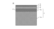
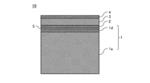
- the laminated body (laminated substrate) 10 (hereinafter, also referred to as the piezoelectric laminated body 10) having the piezoelectric film according to the present embodiment is on the substrate 1 and the substrate 1.
- the substrate 1 is a single crystal silicon (Si) substrate 1a on which a surface oxide film (SiO 2 film) 1b such as a thermal oxide film or a CVD (Chemical Vapor Deposition) oxide film is formed, that is, a Si substrate having a surface oxide film.
- a Si substrate 1a having an insulating film 1d formed of an insulating material other than SiO 2 on its surface can also be used.
- a Si substrate 1a in which a Si (100) surface or a Si (111) surface is exposed on the surface that is, a Si substrate having no surface oxide film 1b or insulating film 1d can also be used.
- the substrate 1 is formed of a metal material such as an SOI (Silicon On Insulator) substrate, a quartz glass (SiO 2 ) substrate, a gallium arsenide (GaAs) substrate, a sapphire (Al 2 O 3 ) substrate, and stainless steel (SUS). It is also possible to use a metal substrate.
- the thickness of the single crystal Si substrate 1a can be, for example, 300 ⁇ m or more and 1000 ⁇ m or less, and the thickness of the surface oxide film 1b can be, for example, 1 nm or more and 4000 nm or less.
- the oxide film 5 is a film containing zinc and oxygen as main elements.
- the oxide film 5 can be formed by using, for example, zinc oxide.
- the (0001) plane of the crystal constituting the ZnO film 5 is parallel to the main surface of the substrate 1.
- the (0001) plane is inclined at an angle within ⁇ 5 ° with respect to the main surface of the substrate 1.
- the crystals constituting the ZnO film 5 are preferentially oriented in the (0001) plane orientation.
- the fact that the crystals constituting the ZnO film 5 are preferentially oriented in the (0001) plane orientation is caused by the crystals oriented in the (0002) plane orientation in the X-ray diffraction pattern obtained by the X-ray diffraction (XRD) measurement. It means that the diffraction peak is in the highest state. That is, it is preferable that the surface of the ZnO film 5 (the surface serving as the base of the lower electrode film 2) is mainly composed of the ZnO (0001) surface.
- the ZnO film 5 can be formed by using a sputtering method, a vapor deposition method, or the like.
- the ZnO film 5 functions as an adhesion film that enhances the adhesion between the substrate 1 and the lower electrode film 2 described later.
- the thickness of the ZnO film 5 can be, for example, 1 nm or more, preferably 2 nm or more.
- the ZnO film 5 can be reliably functioned as the above-mentioned adhesion film, and when the thickness is 2 nm or more, the ZnO film 5 can be used as the above-mentioned adhesion film. It will be possible to make it function more reliably. In addition, it is possible to surely enhance the orientation of the KNN film 3 described later.
- the upper limit of the thickness of the ZnO film 5 is not particularly limited, but from the viewpoint of suppressing a decrease in the productivity of the piezoelectric laminate 10, the thickness of the ZnO film 5 is, for example, 50 nm or less, preferably 20 nm or less, more preferably 10 nm or less. Can be.
- the lower electrode film 2 can be formed by using, for example, platinum (Pt).
- the lower electrode film 2 is a polycrystalline film or a single crystal film (hereinafter, these are also referred to as Pt films).
- the (111) plane of the crystal constituting the Pt film is parallel to the main surface of the substrate 1, and the ((111) plane) is inclined at an angle within ⁇ 5 ° with respect to the main surface of the substrate 1. It is preferable that there are many crystals), that is, the crystals constituting the Pt film are preferentially oriented in the (111) plane orientation.
- the crystal constituting the Pt film is preferentially oriented in the (111) plane orientation, that is, the diffraction peak caused by the crystal oriented in the (111) plane orientation is the highest in the X-ray diffraction pattern obtained by the XRD measurement. Means that it is in. That is, it is preferable that the surface of the lower electrode film 2 (the surface serving as the base of the piezoelectric film 3) is mainly composed of the Pt (111) surface.
- the lower electrode film 2 can be formed by using a sputtering method, a vapor deposition method, or the like.
- the lower electrode film 2 (Pt film) on the ZnO film 5 whose surface is mainly composed of the ZnO (0001) surface, the surface is mainly composed of the Pt (111) surface.
- the lower electrode film 2 can be easily obtained.
- the lower electrode film 2 can also be formed by using various metals such as gold (Au), ruthenium (Ru), and iridium (Ir), and alloys containing these as main components.
- the thickness of the lower electrode film 2 can be, for example, 100 nm or more and 400 nm or less.
- the piezoelectric film 3 is, for example, an alkaline niobium oxide film containing potassium (K), sodium (Na), niobium (Nb), and oxygen (O).
- the piezoelectric film 3 can be formed by using sodium niobate potassium (KNN).
- the piezoelectric film 3 is a KNN polycrystalline film (hereinafter, also referred to as KNN film 3).
- the crystal structure of KNN has a perovskite structure, that is, the KNN film 3 has a perovskite structure.
- the KNN film 3 can be formed by using a method such as a sputtering method, a PLD (Pulsed Laser Deposition) method, or a sol-gel method.
- the thickness of the KNN film 3 can be, for example, 0.5 ⁇ m or more and 5 ⁇ m or less.
- the crystals constituting the KNN film 3 are oriented in the (001) plane direction with respect to the main surface of the substrate 1 (Si substrate 1a when the substrate 1 is, for example, a Si substrate 1a having a surface oxide film 1b or an insulating film 1d). It is preferably preferentially oriented. That is, it is preferable that the surface of the KNN film 3 (the surface serving as the base of the upper electrode film 4) is mainly composed of the KNN (001) surface. For example, by directly forming the KNN film 3 on the Pt film (lower electrode film 2) whose surface is mainly composed of Pt (111) surfaces, the surface is mainly composed of KNN (001) surfaces. The KNN film 3 can be easily obtained.
- the fact that the crystals constituting the KNN film 3 are oriented in the (001) plane orientation means that the (001) planes of the crystals constituting the KNN film 3 are parallel to the main surface of the substrate 1.
- the fact that the (001) plane of the crystal constituting the KNN film 3 is parallel to the main surface of the substrate 1 is other than the case where the (001) plane is completely parallel to the main surface of the substrate 1.
- (001) may be inclined within ⁇ 5 °, preferably within ⁇ 3 °, with respect to the main surface of the substrate 1.
- the fact that the crystals constituting the KNN film 3 are preferentially oriented in the (001) plane direction means that there are many crystals in which the (001) plane is parallel to the main plane of the substrate 1.
- the orientation ratio of the crystals constituting the KNN film 3 in the (001) plane orientation (hereinafter, also referred to as "alignment ratio of the KNN film 3" is preferably, for example, 80% or more, and is, for example, 90% or more. Is more preferable.
- Equation 1 and the "diffraction peak of the (001) plane" in the present specification refer to (001) of the crystals constituting the KNN film 3 in the X-ray diffraction pattern obtained by XRD measurement with respect to the KNN film 3.
- Diffraction peak caused by a crystal oriented in a plane orientation (that is, a crystal whose (001) plane is parallel to the main plane of the substrate 1), and a peak in which 2 ⁇ appears in the range of 20 ° or more and 23 ° or less. Is.
- Equation 1 and the "diffraction peak of the (110) plane" in the present specification are among the crystals constituting the KNN film 3 in the X-ray diffraction pattern obtained by the XRD measurement with respect to the KNN film 3. It is a diffraction peak caused by a crystal oriented in the (110) plane orientation (that is, a crystal in which the (110) plane is parallel to the main plane of the substrate 1), and 2 ⁇ is within the range of 30 ° or more and 33 ° or less. It is the peak that appears.
- the boundary between the crystals constituting the KNN film 3, that is, the grain boundaries existing in the KNN film 3 penetrate in the thickness direction of the KNN film 3.
- the grain boundaries penetrating in the thickness direction of the KNN film 3 are larger than the grain boundaries not penetrating in the thickness direction of the KNN film 3.
- the KNN film 3 contains elements other than K, Na, Nb, and O such as copper (Cu), manganese (Mn), lithium (Li), tantalum (Ta), and antimony (Sb), for example, 5 at% or less (described above). When a plurality of elements are added, the total concentration may be contained within the range of 5 at% or less).
- the upper electrode film 4 can be formed by using, for example, various metals such as Pt, Au, aluminum (Al), and Cu, or alloys thereof.
- the upper electrode film 4 can be formed by using a method such as a sputtering method, a vapor deposition method, a plating method, or a metal paste method.
- the upper electrode film 4 does not have a great influence on the crystal structure of the KNN film 3 like the lower electrode film 2. Therefore, the material, crystal structure, and film forming method of the upper electrode film 4 are not particularly limited.
- an adhesion layer containing iridium oxide (IrO 2 ) or the like as a main component may be provided.
- the thickness of the upper electrode film 4 can be, for example, 100 nm or more and 5000 nm or less, and when the adhesion layer is provided, the thickness of the adhesion layer can be, for example, 1 nm or more and 200 nm or less.
- a film containing Ti as an adhesive film (hereinafter, also simply referred to as “adhesive film”) between the substrate 1 and the lower electrode film 2 to enhance the adhesion between them.
- a ZnO film 5 is provided instead of (for example, a Ti film).
- Zinc oxide (ZnO) is less likely to diffuse than the Ti element, and hardly diffuses to the KNN film 3 through the lower electrode film 2. Therefore, the above-mentioned problems that occur when a Ti film is provided as an adhesion film, for example. Does not occur. Further, since the Zn element is less active than the Ti element, even if it diffuses to the KNN film 3, it is difficult to capture the O element in the KNN film 3 and it is difficult to cause oxygen defects in the KNN film 3. ..
- the ZnO film 5 since the ZnO film 5 is provided, it is possible to increase the number of KNN crystals whose (001) plane is parallel to the main plane of the substrate 1 as compared with the case where the Ti film is provided. That is, it is possible to reduce the number of KNN crystals whose (001) plane is inclined at a predetermined angle with respect to the main plane of the substrate 1. Further, even when the (001) plane of the KNN crystal is tilted at a predetermined angle with respect to the main plane of the substrate 1, the tilt angle can be reduced.
- the diffraction peak on the (001) plane becomes a sharp peak with a narrower half-value width than when the Ti film is provided, and the diffraction peak on the (001) plane.
- the strength increases.
- the provision of the ZnO film 5 makes it possible to set the maximum intensity of the diffraction peak on the (001) plane to 1000 cps or more and 1400 cps or less, preferably 1100 cps or more and 1350 cps or less.
- the number of KNN crystals whose (001) plane is inclined at a predetermined angle with respect to the main surface of the substrate 1 is larger than that when the ZnO film 5 is provided. , The tilt angle also increases. As a result, the diffraction peak on the (001) plane becomes a peak with a wide half-value width, and the peak intensity becomes low. In this case, the maximum intensity of the diffraction peak on the (001) plane is, for example, about 600 cps to 900 cps.
- the ZnO film 5 it is possible to obtain the KNN film 3 having both a high orientation rate and a low relative permittivity. This is because the ZnO film 5 is provided, so that the KNN film 3 maintains the high orientation rate as described above even if the film formation temperature of the KNN film 3 is lowered (for example, even if it is 500 ° C. or lower). It turned out. This is a new finding found for the first time by the inventor and others. Since the ZnO film 5 is provided in this way, the KNN film 3 can be formed at a low temperature without lowering the orientation (orientation ratio) of the KNN film 3, so that the KNN film 3 has a low dielectric constant. It is also possible to make a thin film.
- r can be, for example, 250 or more and 300 or less, preferably 250 or more and less than 300, and more preferably 250 or more and 270 or less.
- the film forming temperature of the KNN film 3 is lowered (for example, set to 500 ° C. or lower), the orientation of the KNN film 3 is lowered. Therefore, when the Ti film is provided, it is necessary to form the KNN film 3 at a high temperature (for example, over 500 ° C.) in order to prevent the orientation of the KNN film 3 from deteriorating, and as a result, the KNN film 3 needs to be formed. Dielectric constant becomes high. In this case, the relative permittivity of the KNN film 3 is, for example, about 300 to 500.
- the diffraction peak intensity of the KNN film 3, for example, the (001) plane, which has both good orientation and a low dielectric constant can be obtained without causing the above-mentioned problems. It is also possible to obtain a KNN film 3 having a high and low dielectric constant.
- FIG. 3 shows a schematic configuration diagram of a device module 30 (hereinafter, also referred to as a piezoelectric device module 30) having a KNN film 3 in the present disclosure.
- the piezoelectric device module 30 includes an element (device) 20 (element 20 having a KNN film 3, hereinafter also referred to as a piezoelectric element 20) obtained by molding the above-mentioned piezoelectric laminate 10 into a predetermined shape, and a piezoelectric element 20. It is provided with at least a voltage application unit 11a or a voltage detection unit 11b connected to the device.
- the voltage application unit 11a is a means for applying a voltage between the lower electrode film 2 and the upper electrode film 4 (between the electrodes)
- the voltage detection unit 11b is a means for applying the voltage between the lower electrode film 2 and the upper electrode film 4. It is a means for detecting the voltage generated between the electrodes (between the electrodes).
- various known means can be used as the voltage application unit 11a and the voltage detection unit 11b.
- the piezoelectric element 20 By connecting the voltage application unit 11a between the lower electrode film 2 and the upper electrode film 4 of the piezoelectric element 20, the piezoelectric element 20 can function as an actuator.
- the KNN film 3 can be deformed by applying a voltage between the lower electrode film 2 and the upper electrode film 4 by the voltage applying portion 11a.
- various members connected to the piezoelectric element 20 can be operated.
- examples of the use of the piezoelectric element 20 include a head for an inkjet printer, a MEMS mirror for a scanner, a vibrator for an ultrasonic generator, and the like.
- the piezoelectric element 20 can function as a sensor.
- a voltage is generated between the lower electrode film 2 and the upper electrode film 4 due to the deformation.
- the magnitude of the physical quantity applied to the KNN film 3 can be measured.
- applications of the piezoelectric element 20 include, for example, an angular velocity sensor, an ultrasonic sensor, a pressure sensor, an acceleration sensor, and the like.
- the piezoelectric laminate 10 is provided with the ZnO film 5 instead of the Ti film as the adhesion film, the vicinity of the interface between the KNN film 3 and the lower electrode film 2 in the KNN film 3 in particular. There are few oxygen defects present in. As a result, the piezoelectric element 20 obtained by processing the piezoelectric laminate 10 is less likely to undergo dielectric breakdown even when a positive voltage is applied.
- a substrate 1 is prepared, and a ZnO film 5 is formed on one of the main surfaces of the substrate 1 by, for example, a sputtering method.
- a sputtering method For example, using a target material made of zinc oxide, the atmosphere of a mixed gas of argon (Ar) gas and oxygen (O 2 ) gas (hereinafter, also referred to as “Ar / O 2 mixed gas atmosphere”) is obtained by the RF sputtering method.
- Ar argon
- O 2 oxygen
- the following conditions are exemplified as the conditions for forming the ZnO film 5.
- the film forming time of the ZnO film 5 can be appropriately set according to the thickness of the ZnO film 5.
- the film-forming rate can be, for example, the rate at which a ZnO film having a thickness of 2.5 nm is formed in 30 seconds.
- Atmosphere 100 W or higher and 500 W or lower, preferably 200 W or higher and 400 W or lower
- Atmosphere Ar / O 2 mixture Gas atmosphere
- Atmospheric pressure 0.1 Pa or more and 0.5 Pa or less, preferably 0.2 Pa or more and 0.4 Pa or less
- the crystals constituting the ZnO film 5 can be preferentially oriented in the (0001) plane orientation. That is, by forming the ZnO film 5 in a state where the substrate 1 is heated, it is possible to obtain the ZnO film 5 having high orientation. Further, by forming the ZnO film 5 under a temperature condition of, for example, 300 ° C. or higher, the orientation of the ZnO film 5 can be further enhanced. Further, by forming the ZnO film 5 under a temperature condition of, for example, 500 ° C. or higher, the orientation of the ZnO film 5 can be further enhanced.
- the film forming temperature of the ZnO film 5 is preferably 700 ° C. or lower.
- a lower electrode film 2 (for example, a Pt film) is formed on the ZnO film 5 in which the crystals are preferentially oriented in the (0001) plane direction, for example, by a sputtering method.
- Atmosphere Ar gas atmosphere
- Atmospheric pressure 0.1 Pa or more and 0.5 Pa or less, preferably 0.2 Pa or more and 0.4 Pa or less
- the crystals constituting the Pt film can be preferentially oriented in the (111) plane orientation. That is, by forming a Pt film in a state where the substrate 1 is heated, it is possible to obtain a Pt film having high orientation. Further, by forming the Pt film under a temperature condition of, for example, 300 ° C. or higher, the orientation of the Pt film can be further enhanced. Further, by forming the Pt film under a temperature condition of, for example, 500 ° C. or higher, the orientation of the Pt film can be further enhanced.
- the film formation temperature of the Pt film As described above, the higher the film formation temperature of the Pt film, the higher the orientation of the Pt film tends to be. However, even if the film formation temperature of the Pt film exceeds 700 ° C., the orientation of the Pt film is enhanced. While the effect has reached a plateau, it takes time to lower the temperature in the atmosphere from the film forming temperature of the Pt film to the film forming temperature of the KNN film 3 described later, and as a result, the productivity of the piezoelectric laminate 10 is increased. May decrease. Therefore, the film forming temperature of the Pt film is preferably 700 ° C. or lower.
- the KNN film 3 is formed on the Pt film in which the crystals are preferentially oriented in the (111) plane direction in advance, for example, by a sputtering method.
- the composition ratio of the KNN film 3 can be adjusted, for example, by controlling the composition of the target material used during sputtering film formation.
- the target material can be produced by mixing K 2 CO 3 powder, Na 2 CO 3 powder, Nb 2 O 5 powder and the like and firing them.
- the composition of the target material can be controlled by adjusting the mixing ratio of K 2 CO 3 powder, Na 2 CO 3 powder, Nb 2 O 5 powder and the like.
- the material may be used.
- the film forming time can be appropriately set according to the thickness of the KNN film 3.
- Discharge power 2000 W or more and 2400 W or less, preferably 2100 W or more and 2300 W or less
- Atmosphere Ar gas + oxygen (O 2 ) gas atmosphere
- Atmospheric pressure 0.2 Pa or more and 0.5 Pa or less, preferably 0.2 Pa or more and 0.4 Pa or less
- O 2 Partial pressure of Ar gas to gas (Ar / O 2 partial pressure ratio): 30/1 to 20/1, preferably 27/1 to 22/1
- Film formation temperature 430 ° C or more and 700 ° C or less
- Film formation speed 0.5 ⁇ m / hr or more and 2 ⁇ m / hr or less, preferably 0.75 ⁇ m / hr or more and 1.5 ⁇ m / hr or less
- the crystals constituting the KNN film 3 are prioritized in the (001) plane orientation. It can be oriented.
- the film is formed on the lower electrode film 2. It is possible to increase the orientation of the KNN film 3 to be formed. As a result, for example, 80% or more of the crystals constituting the KNN film 3 can be oriented in the (001) plane orientation. That is, it is possible to obtain the KNN film 3 having the above-mentioned orientation ratio of, for example, 80% or more.
- the film-forming temperature of the lower electrode film 2 can be made lower than the film-forming temperature of the ZnO film 5.
- the ZnO film 5 and the lower electrode film 2 under temperature conditions of 300 ° C. or higher, for example, 80% or more of the crystals constituting the KNN film 3 are oriented in the (001) plane orientation. It is possible to reliably orient the film. That is, it is possible to reliably obtain the KNN film 3 having the above-mentioned orientation ratio of, for example, 80% or more.
- the ZnO film 5 and the lower electrode film 2 under temperature conditions of 500 ° C. or higher, for example, 85% or more, preferably 90% or more of the crystals constituting the KNN film 3 are formed.
- the film forming temperature of the KNN film 3 is preferably 500 ° C. or higher and 700 ° C. or lower, and more preferably 540 ° C. or higher and 700 ° C. or lower. This makes it possible to surely increase the withstand voltage of the KNN film 3 when a positive voltage is applied.
- the film forming temperature of the KNN film 3 is preferably 430 ° C. or higher and 500 ° C. or lower, and more preferably 440 ° C. or higher and 470 ° C. or lower. Since the ZnO film 5 is provided, it is possible to make the KNN film 3 a highly oriented film even if the film forming temperature of the KNN film 3 is lowered in this way. Further, by forming the KNN film 3 at such a low temperature, the KNN film 3 can be made into a film having a low dielectric constant. That is, it is possible to obtain a KNN film 3 having both a high orientation rate and a low dielectric constant that can be suitably used as a sensor.
- the upper electrode film 4 is formed on the KNN film 3 by, for example, a sputtering method.
- the conditions for forming the upper electrode film 4 can be the same as the conditions for forming the lower electrode film 2 described above.
- the ZnO film 5, the lower electrode film 2 (Pt film), the KNN film 3, and the upper electrode film 4 are formed on the substrate 1 in this order, thereby forming a piezoelectric film as shown in FIG.
- the laminated body 10 is obtained.
- the obtained piezoelectric laminate 10 is molded into a predetermined shape by etching or the like (microfabrication is performed on a predetermined pattern).
- the piezoelectric element 20 as shown in FIG. 3 is obtained, and the piezoelectric device module 30 can be obtained by connecting the voltage application unit 11a or the voltage detection unit 11b to the piezoelectric element 20.
- the etching method for example, a dry etching method such as reactive ion etching or a wet etching method using a predetermined etching solution can be used.
- a photoresist pattern as an etching mask for dry etching is formed on the piezoelectric laminate 10 (for example, the upper electrode film 4) by a photolithography process or the like.
- a noble metal film such as a chromium (Cr) film, a nickel (Ni) film, a platinum (Pt) film, and a Ti film may be formed by a sputtering method.
- dry etching is performed on the piezoelectric laminate 10 (upper electrode film 4, KNN film 3, etc.) using a gas containing a halogen element as the etching gas.
- the halogen element includes chlorine (Cl), fluorine (F) and the like.
- the gas containing a halogen element BCl 3 gas, SiC 4 gas, chlorine (Cl 2 ) gas, CF 4 gas, C 4 F 8 gas and the like can be used.
- a silicon oxide (SiO x ) film or the like as an etching mask for wet etching is formed on the piezoelectric laminate 10 (for example, the upper electrode film 4). Then, for example, the piezoelectric laminate 10 is immersed in an etching solution containing an alkaline aqueous solution of a chelating agent and not containing hydrofluoric acid, and wet etching is performed on the piezoelectric laminate 10 (upper electrode film 4, KNN film 3, etc.).
- etching solution containing an alkaline aqueous solution of a chelating agent and not containing hydrofluoric acid an etching solution obtained by mixing ethylenediaminetetraacetic acid as a chelating agent, aqueous ammonia, and aqueous hydrogen peroxide can be used.
- the Ti film is provided by providing the ZnO film 5 instead of the film containing Ti (for example, the Ti film) as the adhesion film that adheres the substrate 1 and the lower electrode film 2 to each other. Adhesion of the same level or higher can be maintained.
- the adhesive film is composed of the ZnO film 5, so that the element that diffuses into the KNN film 3 is more difficult than when the adhesive film is composed of the Ti film. Can be reduced. This makes it possible to suppress the generation of oxygen defects in the KNN film 3, especially in the vicinity of the interface between the KNN film 3 and the lower electrode film 2.
- the withstand voltage of the KNN film 3 when a positive voltage is applied can be increased, and the deterioration of the insulating property when a positive voltage is applied can be avoided. That is, in the piezoelectric element 20 obtained by processing the above-mentioned piezoelectric laminated body 10, dielectric breakdown is less likely to occur even when a positive voltage is applied.
- an electric field of 300 kV / cm (from the upper electrode film 4 to the lower part) between the lower electrode film 2 and the upper electrode film 4 in a state where the piezoelectric laminate 10 (piezoelectric element 20) is heated to a temperature of 200 ° C.
- a high acceleration life test (Highly Accelerated Life Test, abbreviated as HALT) is performed in which a positive voltage is applied to the upper electrode film 4 while the lower electrode film 2 is grounded so as to generate an electric field toward the electrode film 2.
- HALT Highly Accelerated Life Test
- the time from the start of voltage application to the destruction of the insulation of the KNN film 3 can be set to 1500 seconds or more.
- the KNN film 3 has undergone dielectric breakdown when the leakage current density flowing through the KNN film 3 exceeds 30 mA / cm 2.
- a film containing no Ti containing tantalum (Ta), tantalum oxide (Ta 2 O 5 ), nickel (Ni) or the like as a main component, or a titanium oxide (TiO 2 ) film may be formed. Proposed.
- these films have a problem that the adhesion is clearly weaker than that of the Ti film and the ZnO film 5.
- the ZnO film 5 is provided as the adhesion film, it is possible to maintain the adhesion equal to or higher than that of the Ti film.
- the KNN film 3 can be made into a film having a high diffraction peak intensity on the (001) plane.
- the maximum intensity of the diffraction peak on the (001) plane can be 1000 cps or more and 1400 cps or less.
- the ZnO film 5 is provided as an adhesion film for bringing the substrate 1 and the lower electrode film 2 into close contact with each other, so that the KNN film 3 has both a high orientation rate and a low dielectric constant. It becomes possible. This is because the provision of the ZnO film 5 makes it possible to form the KNN film 3 at a low temperature without lowering the orientation ratio of the KNN film 3. Since the KNN film 3 can be formed at a low temperature, the KNN film 3 can be made into a film having a low dielectric constant.
- the relative permittivity of the KNN film 3 when measured by applying a voltage of -1V to + 1V with a triangular wave having a frequency of 3 kHz with the lower electrode film 2 as the ground can be set to 250 or more and 300 or less.
- the piezoelectric laminate 10 having such a KNN film 3 can be particularly suitably used for applications such as high-sensitivity sensors that require a low dielectric constant.
- the piezoelectric element 20 in which the HALT result under predetermined conditions is 1500 seconds or longer, preferably 1600 seconds or longer, when the orientation rate of the crystals constituting the KNN film 3 in the (001) plane direction is 80% or more. Can be obtained. Further, when the orientation rate of the crystals constituting the KNN film 3 in the (001) plane direction is 90% or more, it is possible to obtain the piezoelectric element 20 in which the HALT result under predetermined conditions is 1800 seconds or more. ..
- the ZnO film 5 When the thickness of the ZnO film 5 is, for example, 1 nm or more, the ZnO film 5 can be reliably functioned as an adhesive film that adheres the substrate 1 and the lower electrode film 2 to each other. As a result, it is possible to reliably prevent the lower electrode film 2 from peeling off from the substrate 1 during the manufacturing process of the piezoelectric laminate 10, the piezoelectric element 20, and the piezoelectric device module 30 or when a voltage is applied. Further, when the thickness of the ZnO film 5 is, for example, 1 nm or more, the orientation of the KNN film 3 can be further enhanced.
- the lower electrode film 2 can be formed by using a metal oxide such as strontium ruthenate (SrRuO 3 , abbreviated as SRO) or lanthanum nickelate (LaNiO 3, abbreviated as LNO).
- a metal oxide such as strontium ruthenate (SrRuO 3 , abbreviated as SRO) or lanthanum nickelate (LaNiO 3, abbreviated as LNO).
- SRO strontium ruthenate
- LaNiO 3 lanthanum nickelate
- LNO lanthanum nickelate
- the lower electrode film 2 by forming the lower electrode film 2 under the same temperature conditions as in the above aspect, the lower electrode film 2 preferentially oriented in the (001) plane direction can be formed.
- the lower electrode film 2 may be a single-layer film formed by using the above-mentioned various metals or metal oxides, or on a metal film and a metal film formed by using a metal such as Pt. It may be a laminate with a provided film made of SRO, a laminate made of a metal film and a film made of LNO provided on the metal film, or the like. Also in this aspect, the same effect as the above-mentioned aspect can be obtained.
- the piezoelectric element 20 produced by using the piezoelectric laminate 10 can be applied to a desired application such as a sensor or an actuator, as long as the piezoelectric laminate 10 can be applied.
- the substrate 1 may be removed from 10.
- a Si substrate having a surface oriented in (100) plane orientation, a thickness of 610 ⁇ m, a diameter of 6 inches, and a thermal oxide film (SiO 2 film) having a thickness of 200 nm formed on the surface is prepared. did. Then, on this substrate (on the thermal oxide film), the first adhesive film, the Pt film as the lower electrode film (thickness: 200 nm), the KNN film as the piezoelectric film (thickness: 2 ⁇ m), and the second adhesive film. RuO 2 film (thickness: 10 nm) and Pt film (thickness: 100 nm) as the upper electrode film were formed in this order to prepare a piezoelectric laminate (samples 1 to 16).
- the first adhesive film is a film for adhering the substrate and the lower electrode film
- the second adhesive film is a film for adhering the KNN film and the upper electrode film.
- a ZnO film or a Ti film was formed as the first adhesion film. Further, the thickness of the first adhesive film was changed within the range of 0.5 nm or more and 50 nm or less.
- the first adhesion film (ZnO film or Ti film) was formed by the RF magnetron sputtering method.
- the conditions for forming the first adhesive film were as follows. Among the following conditions, the film forming temperature means the temperature of the heater of the sputtering apparatus (the same applies to the conditions of other films). Further, the film forming temperature of room temperature means that the first adhesive film is formed in a non-heated state. Further, the film forming time was appropriately changed according to the thickness of the first adhesive film to be formed.
- Film formation temperature Predetermined temperature within the range of room temperature (for example, 28 ° C) or more and 700 ° C or less Atmosphere of mixed gas of Ar gas and O 2 gas Introduced gas: Ar gas: 100 cc, O 2 gas: 10 cc Atmospheric pressure: 0.2Pa Discharge power: 300W Film formation rate: The rate at which the first adhesive film with a thickness of 2.5 nm is formed in 30 seconds.
- the lower electrode film and the upper electrode film were formed by the RF magnetron sputtering method.
- the conditions for forming the lower electrode film and the upper electrode film were as follows. Film formation temperature: 300 ° C Discharge power: 1200W Introduced gas: Ar gas Atmospheric pressure: 0.3Pa Film formation time: 5 minutes
- the KNN film was formed by the RF magnetron sputtering method.
- a Na x ) NbO 3 sintered body was used.
- K 2 CO 3 powder, Na 2 CO 3 powder, and Nb 2 O 5 powder were mixed for 24 hours using a ball mill, calcined at 850 ° C. for 10 hours, and then pulverized again with a ball mill. , 200 MPa, and then calcined at 1080 ° C. to produce.
- the composition of the target material is controlled by adjusting the mixing ratio of K 2 CO 3 powder, Na 2 CO 3 powder, and Nb 2 O 5 powder, and EDX (energy dispersive X-ray spectroscopic analysis) is performed before the film formation process. ).
- the conditions for forming the KNN film were as follows. Film formation temperature: 550 ° C Discharge power: 2200W Introduced gas: Mixed gas atmosphere pressure of Ar gas and O 2 gas: 0.3Pa The partial pressure ratio of Ar gas to the O 2 gas (Ar gas partial pressure / O 2 gas partial pressure): 25/1 Film formation speed: 1 ⁇ m / hr
- the orientation of the KNN film was evaluated by measuring the orientation rate of the crystals constituting the KNN film in the (001) plane orientation.
- the orientation ratio of the KNN film was measured by XRD for each sample to obtain an X-ray diffraction pattern.
- the conditions for XRD measurement were as follows.
- Output current 22mA KNN film thickness: 2um
- Equation 1 Calculated according to the above (Equation 1) based on the peak intensity of the obtained diffraction pattern.
- the calculation results of the orientation rate are as shown in Table 1 above.
- the orientation of the KNN film can be enhanced by forming the ZnO film and the lower electrode film at a temperature of 200 ° C. or higher, respectively. It was confirmed that a KNN film having the above-mentioned orientation ratio of 80% or more could be obtained. If the ZnO film and the lower electrode film are formed in a non-heated state or at a temperature of less than 200 ° C., the orientation of the KNN film cannot be improved and the orientation rate becomes less than 80%. I was able to confirm that.
- the orientation of the KNN film is higher than that in the case of forming a film at a temperature of 200 ° C. It was confirmed that the sex could be further enhanced.
- the orientation of the KNN film is further improved by forming the ZnO film and the lower electrode film as the first adhesion film at a temperature of 500 ° C. or higher (for example, 500 ° C., 700 ° C.). It was confirmed that the KNN film having the above-mentioned orientation ratio of 90% or more could be obtained.
- the orientation rate of the KNN film is less than 80% even when the film formation temperature of the Ti film and the lower electrode film is 500 ° C. I was able to confirm that there were cases.
- the thickness of the ZnO film as the first adhesion film is 1 nm or more, the adhesion force equal to or higher than that when the Ti film is provided as the first adhesion film is maintained. I was able to confirm that it was possible.
- the thickness of the ZnO film as the first adhesion film was less than 1 nm (for example, 0.5 nm), it was confirmed that the adhesion was weak and there was a part where the lower electrode film was peeled off from the substrate. Further, it was confirmed that even when a Ti film having a thickness of 1 nm was provided as the first adhesive film, there was a part where the lower electrode film was peeled off from the substrate.
- the evaluation of the insulation property when a positive voltage is applied is to evaluate the electric field of 300 kV / cm between the lower electrode film and the upper electrode film in a state where the temperature of each piezoelectric laminate (each sample) is heated to 200 ° C.
- HALT is performed in which a positive voltage is applied to the upper electrode film while the lower electrode film is grounded so as to generate an electric field from the upper electrode film to the lower electrode film
- the KNN film is insulated from the start of voltage application. This was done by measuring the time to destruction.
- the leakage current density flowing through the KNN film exceeded 30 mA / cm 2 , it was considered that the KNN film had undergone dielectric breakdown.
- HALT life The time until the KNN film measured by HALT under the above conditions reaches dielectric breakdown is defined as "HALT life”.
- HALT lifetime of each sample is as shown in Table 1. These HALT lifetimes (measurement results) are the average of the values measured at 7 points within 0.5 mm ⁇ for each sample. The description of "1800 seconds or more" in Table 1 means that dielectric breakdown did not occur even after 1800 seconds had passed from the start of voltage application.
- the orientation ratio of the KNN film is 80% or more, and the HALT life is 1500 seconds or longer. It was confirmed that a piezoelectric laminate (KNN film) was obtained.
- the orientation rate of the KNN film is 90% and the HALT life is 1800 seconds or longer. It was confirmed that a laminated body was obtained.
- the thickness of the ZnO film is less than 1 nm (for example, 0.5 nm)
- the alignment rate of the KNN film is 85% or more by forming the ZnO film and the lower electrode film under the temperature condition of 500 ° C. or higher. It was confirmed that a piezoelectric laminate having a HALT life of 1700 seconds or more could be obtained.
- the orientation ratio of the KNN film is 90% or more and the HALT life is long even if the ZnO film and the lower electrode film are formed under a temperature condition of 500 ° C. or higher. It has been confirmed that it is difficult to obtain a piezoelectric laminate that takes 1800 seconds or more.
- the thickness of the ZnO film or the Ti film as the first adhesion film was as shown in Table 2 below, and the film formation temperature of the first adhesion film was 500 ° C. Further, the film forming temperature of the lower electrode film was set to 500 ° C. Further, the film forming temperature of the KNN film was set to 460 ° C. Other methods and conditions were the same as those of Samples 1 to 16 described above.
- the measurement of the orientation ratio of the crystals constituting the KNN film in the (001) plane orientation was performed by the same method and conditions as the measurement of the orientation ratio of the samples 1 to 16.
- the diffraction peak intensity of the (001) plane of the KNN film was measured by XRD for each of the samples 17 to 21 to obtain an X-ray diffraction pattern (2 ⁇ / ⁇ ), and in the obtained X-ray diffraction pattern, 2 ⁇ .
- the conditions for XRD measurement were as follows.
- Output current 22mA KNN film thickness: 2um
- the relative permittivity was measured by applying a voltage of -1V to + 1V to the upper electrode film 4 with a triangular wave having a frequency of 3 kHz with the lower electrode film 2 as the ground.
- the measurement results of the orientation rate, diffraction peak intensity, and relative permittivity are as shown in Table 2 above.
- the “001 intensity” in Table 2 means the diffraction peak intensity of the (001) plane of the KNN film.
- the ZnO film is provided as the first adhesion film, the orientation of the KNN film is lowered even when the film formation temperature of the KNN film is low (500 ° C. or lower, for example, 460 ° C.). I was able to confirm that there was nothing. That is, by providing the ZnO film, even if the KNN film is formed at a low temperature, the maximum intensity of the diffraction peak of the (001) plane can be 1000 cps or more and 1400 cps or less, preferably 1100 cps or more and 1350 cps or less. Was confirmed.
- the relative permittivity of the KNN film can be lowered by forming the KNN film at a low temperature. That is, it was confirmed that the relative permittivity can be 250 or more and 300 or less, preferably 250 or more and less than 300, and more preferably 250 or more and 270 or less.
- the KNN film can be formed at a low temperature without deteriorating the orientation of the KNN film by providing the ZnO film. That is, it was confirmed that the KNN film having both a high orientation rate and a low dielectric constant can be obtained by providing the ZnO film.
- Such a KNN film can be particularly suitably used for applications of high-sensitivity sensors.
- Appendix 2 The piezoelectric laminate according to Appendix 1, preferably.
- the orientation ratio of the crystals constituting the piezoelectric film in the (001) plane direction is 80% or more.
- Appendix 3 The piezoelectric laminate according to Appendix 1 or 2, preferably.
- the upper electrode film is provided on the piezoelectric film so as to generate an electric field of 300 kV / cm between the upper electrode film, which is a film different from the electrode film, and the electrode film.
- the time from the start of voltage application until the leakage current density flowing through the piezoelectric film exceeds 30 mA / cm 2 is 1500 seconds or more, preferably 1600 seconds or more.
- the piezoelectric laminate according to Appendix 4 preferably.
- the upper electrode film is provided on the piezoelectric film at a temperature of 200 ° C., and an electric field of 300 kV / cm is generated between the upper electrode film, which is an electrode film different from the electrode film, and the electrode film.
- the time from the start of voltage application until the leakage current density flowing through the piezoelectric film exceeds 30 mA / cm 2 is 1800 seconds or more.
- a positive voltage is applied to the upper electrode film so as to generate an electric field of 300 kV / cm between the upper electrode film and the lower electrode film at a temperature of 200 ° C.
- the piezoelectricity is applied from the start of voltage application.
- the time required for the leakage current density flowing through the film to exceed 30 mA / cm 2 is 1500 seconds or longer, preferably 1600 seconds or longer.
- (Appendix 12) The piezoelectric element or piezoelectric device module according to Appendix 9, preferably.
- the orientation rate of the crystals constituting the piezoelectric film in the (001) plane direction is 90% or more.
- Appendix 13 The piezoelectric element or piezoelectric device module according to Appendix 12, preferably.
- a positive voltage is applied to the upper electrode film so as to generate an electric field of 300 kV / cm between the upper electrode film and the lower electrode film at a temperature of 200 ° C.
- the piezoelectricity is applied from the start of voltage application. It takes 1800 seconds or more for the leakage current density flowing through the membrane to exceed 30 mA / cm 2.
- the oxide film is formed under a temperature condition of 200 ° C. or higher.
- the electrode film is formed under a temperature condition of 200 ° C. or higher.
- the crystals constituting the oxide film are preferentially oriented in the (0001) plane orientation.
- the crystals constituting the electrode film are preferentially oriented in a predetermined direction.
- the crystals constituting the electrode film are preferentially oriented in the (111) plane orientation, and a predetermined electrode film is formed.
- the crystals constituting the electrode film are preferentially oriented in the (001) plane orientation.
Landscapes
- Chemical & Material Sciences (AREA)
- Engineering & Computer Science (AREA)
- Organic Chemistry (AREA)
- Materials Engineering (AREA)
- Chemical Kinetics & Catalysis (AREA)
- Mechanical Engineering (AREA)
- Metallurgy (AREA)
- Ceramic Engineering (AREA)
- Manufacturing & Machinery (AREA)
- Inorganic Chemistry (AREA)
- Structural Engineering (AREA)
- Physical Vapour Deposition (AREA)
Priority Applications (3)
| Application Number | Priority Date | Filing Date | Title |
|---|---|---|---|
| EP21832995.1A EP4174024A4 (en) | 2020-06-30 | 2021-03-16 | Piezoelectric laminate, piezoelectric element, and method for manufacturing piezoelectric laminate |
| US18/012,920 US20230270013A1 (en) | 2020-06-30 | 2021-03-16 | Piezoelectric stack, piezoelectric element, and method of manufacturing piezoelectric stack |
| JP2022533684A JP7696347B2 (ja) | 2020-06-30 | 2021-03-16 | 圧電積層体、圧電素子および圧電積層体の製造方法 |
Applications Claiming Priority (2)
| Application Number | Priority Date | Filing Date | Title |
|---|---|---|---|
| JP2020-112459 | 2020-06-30 | ||
| JP2020112459 | 2020-06-30 |
Publications (1)
| Publication Number | Publication Date |
|---|---|
| WO2022004068A1 true WO2022004068A1 (ja) | 2022-01-06 |
Family
ID=79315729
Family Applications (1)
| Application Number | Title | Priority Date | Filing Date |
|---|---|---|---|
| PCT/JP2021/010500 Ceased WO2022004068A1 (ja) | 2020-06-30 | 2021-03-16 | 圧電積層体、圧電素子および圧電積層体の製造方法 |
Country Status (5)
| Country | Link |
|---|---|
| US (1) | US20230270013A1 (https=) |
| EP (1) | EP4174024A4 (https=) |
| JP (1) | JP7696347B2 (https=) |
| TW (1) | TWI870582B (https=) |
| WO (1) | WO2022004068A1 (https=) |
Families Citing this family (2)
| Publication number | Priority date | Publication date | Assignee | Title |
|---|---|---|---|---|
| DE102023207688A1 (de) * | 2023-08-10 | 2025-02-13 | Robert Bosch Gesellschaft mit beschränkter Haftung | Vorrichtung und Verfahren zur Regeneration eines Kalium-Natrium-Niobat-Dünnfilms |
| CN119615085B (zh) * | 2024-11-21 | 2025-09-09 | 武汉大学 | 一种可激发纯横波的ZnO压电涂层材料及其制备方法和应用 |
Citations (6)
| Publication number | Priority date | Publication date | Assignee | Title |
|---|---|---|---|---|
| JP2007184513A (ja) | 2005-12-06 | 2007-07-19 | Seiko Epson Corp | 圧電体積層体、表面弾性波素子、薄膜圧電共振子および圧電アクチュエータ |
| JP2008159807A (ja) | 2006-12-22 | 2008-07-10 | Hitachi Cable Ltd | 圧電薄膜素子及び圧電薄膜素子を用いて製造したアクチュエータとセンサ |
| JP2015530728A (ja) * | 2012-07-31 | 2015-10-15 | Tdk株式会社 | 圧電素子、圧電アクチュエータ、ハードディスクドライブ、インクジェットプリンタ装置、および圧電センサ |
| JP2017076730A (ja) * | 2015-10-16 | 2017-04-20 | 株式会社サイオクス | 圧電薄膜付き積層基板、圧電薄膜素子およびその製造方法 |
| JP2018093145A (ja) * | 2016-12-07 | 2018-06-14 | Tdk株式会社 | 圧電薄膜積層体、圧電薄膜基板、圧電薄膜素子、圧電アクチュエータ、圧電センサ、ヘッドアセンブリ、ヘッドスタックアセンブリ、ハードディスクドライブ、プリンタヘッド、及びインクジェットプリンタ装置 |
| JP2018207055A (ja) * | 2017-06-09 | 2018-12-27 | 株式会社サイオクス | 圧電膜を有する積層基板、圧電膜を有する素子および圧電膜を有する積層基板の製造方法 |
Family Cites Families (10)
| Publication number | Priority date | Publication date | Assignee | Title |
|---|---|---|---|---|
| US7067965B2 (en) * | 2002-09-18 | 2006-06-27 | Tdk Corporation | Piezoelectric porcelain composition, piezoelectric device, and methods of making thereof |
| US20060202769A1 (en) * | 2003-03-31 | 2006-09-14 | Keigo Nagao | Piezoelectric thin film device and method of producing the same |
| JP4600650B2 (ja) * | 2003-11-05 | 2010-12-15 | セイコーエプソン株式会社 | 圧電体膜、圧電素子、圧電アクチュエーター、圧電ポンプ、インクジェット式記録ヘッド、インクジェットプリンター、表面弾性波素子、薄膜圧電共振子、周波数フィルタ、発振器、電子回路、および電子機器 |
| JP4344942B2 (ja) * | 2004-12-28 | 2009-10-14 | セイコーエプソン株式会社 | インクジェット式記録ヘッドおよび圧電アクチュエーター |
| US7525239B2 (en) * | 2006-09-15 | 2009-04-28 | Canon Kabushiki Kaisha | Piezoelectric element, and liquid jet head and ultrasonic motor using the piezoelectric element |
| JP6690193B2 (ja) * | 2014-11-12 | 2020-04-28 | Tdk株式会社 | 圧電体層、圧電素子、圧電アクチュエータ、及び圧電センサ、並びにハードディスクドライブ、及びインクジェットプリンタ装置 |
| JP6790749B2 (ja) * | 2016-11-16 | 2020-11-25 | セイコーエプソン株式会社 | 圧電素子及び圧電素子応用デバイス |
| JP2019021994A (ja) * | 2017-07-12 | 2019-02-07 | 株式会社サイオクス | 圧電膜を有する積層基板、圧電膜を有する素子および圧電膜を有する積層基板の製造方法 |
| JP7044600B2 (ja) * | 2018-03-14 | 2022-03-30 | 住友化学株式会社 | 圧電積層体、圧電積層体の製造方法および圧電デバイス |
| JP7352347B2 (ja) * | 2018-12-07 | 2023-09-28 | 住友化学株式会社 | 圧電積層体、圧電素子および圧電積層体の製造方法 |
-
2021
- 2021-03-16 US US18/012,920 patent/US20230270013A1/en active Pending
- 2021-03-16 EP EP21832995.1A patent/EP4174024A4/en active Pending
- 2021-03-16 JP JP2022533684A patent/JP7696347B2/ja active Active
- 2021-03-16 WO PCT/JP2021/010500 patent/WO2022004068A1/ja not_active Ceased
- 2021-04-20 TW TW110114095A patent/TWI870582B/zh active
Patent Citations (6)
| Publication number | Priority date | Publication date | Assignee | Title |
|---|---|---|---|---|
| JP2007184513A (ja) | 2005-12-06 | 2007-07-19 | Seiko Epson Corp | 圧電体積層体、表面弾性波素子、薄膜圧電共振子および圧電アクチュエータ |
| JP2008159807A (ja) | 2006-12-22 | 2008-07-10 | Hitachi Cable Ltd | 圧電薄膜素子及び圧電薄膜素子を用いて製造したアクチュエータとセンサ |
| JP2015530728A (ja) * | 2012-07-31 | 2015-10-15 | Tdk株式会社 | 圧電素子、圧電アクチュエータ、ハードディスクドライブ、インクジェットプリンタ装置、および圧電センサ |
| JP2017076730A (ja) * | 2015-10-16 | 2017-04-20 | 株式会社サイオクス | 圧電薄膜付き積層基板、圧電薄膜素子およびその製造方法 |
| JP2018093145A (ja) * | 2016-12-07 | 2018-06-14 | Tdk株式会社 | 圧電薄膜積層体、圧電薄膜基板、圧電薄膜素子、圧電アクチュエータ、圧電センサ、ヘッドアセンブリ、ヘッドスタックアセンブリ、ハードディスクドライブ、プリンタヘッド、及びインクジェットプリンタ装置 |
| JP2018207055A (ja) * | 2017-06-09 | 2018-12-27 | 株式会社サイオクス | 圧電膜を有する積層基板、圧電膜を有する素子および圧電膜を有する積層基板の製造方法 |
Non-Patent Citations (1)
| Title |
|---|
| See also references of EP4174024A4 |
Also Published As
| Publication number | Publication date |
|---|---|
| TW202203479A (zh) | 2022-01-16 |
| US20230270013A1 (en) | 2023-08-24 |
| TWI870582B (zh) | 2025-01-21 |
| EP4174024A1 (en) | 2023-05-03 |
| JP7696347B2 (ja) | 2025-06-20 |
| JPWO2022004068A1 (https=) | 2022-01-06 |
| EP4174024A4 (en) | 2024-10-09 |
Similar Documents
| Publication | Publication Date | Title |
|---|---|---|
| JP6239566B2 (ja) | 圧電薄膜付き積層基板、圧電薄膜素子およびその製造方法 | |
| JP6342040B1 (ja) | 圧電膜を有する積層基板、圧電膜を有する素子および圧電膜を有する積層基板の製造方法 | |
| JP7074512B2 (ja) | 圧電積層体、圧電積層体の製造方法、圧電素子、およびスパッタリングターゲット材 | |
| JP7362339B2 (ja) | 圧電積層体、圧電素子、および圧電積層体の製造方法 | |
| TW202505987A (zh) | 壓電積層體、壓電積層體的製造方法、及壓電元件 | |
| WO2022004068A1 (ja) | 圧電積層体、圧電素子および圧電積層体の製造方法 | |
| JP7022853B2 (ja) | スパッタリングターゲット材、スパッタリングターゲット材の製造方法、および圧電薄膜付き積層基板の製造方法 | |
| US20210005805A1 (en) | Piezoelectric laminate, piezoelectric element and method of manufacturing the piezoelectric laminate | |
| JP6502460B2 (ja) | 圧電薄膜付き積層基板および圧電薄膜素子 | |
| TWI888493B (zh) | 壓電膜、壓電積層體、壓電元件及壓電積層體的製造方法 | |
| JP6758444B2 (ja) | 圧電薄膜付き積層基板および圧電薄膜素子 | |
| JP6607993B2 (ja) | 圧電膜を有する積層基板、圧電膜を有する素子および圧電膜を有する積層基板の製造方法 | |
| JP6804615B2 (ja) | 圧電膜を有する積層基板、圧電膜を有する素子および圧電膜を有する積層基板の製造方法 | |
| JP6961770B2 (ja) | 圧電薄膜付き積層基板および圧電薄膜素子 | |
| JP7319848B2 (ja) | 圧電積層体、圧電素子および圧電積層体の製造方法 | |
| JP7626383B2 (ja) | 圧電積層体、圧電素子および圧電積層体の製造方法 | |
| JP2021141186A (ja) | 圧電膜、圧電積層体、圧電素子および圧電積層体の製造方法 | |
| JP2022084768A (ja) | 圧電積層体、圧電積層体の製造方法および圧電デバイス | |
| WO2021002434A1 (ja) | 圧電膜、圧電積層体、圧電素子および圧電積層体の製造方法 | |
| JP2024141259A (ja) | 圧電積層体、圧電積層体の製造方法、及び圧電素子 | |
| JP2022065018A (ja) | 圧電薄膜付き積層基板、圧電薄膜付き積層基板の製造方法、圧電薄膜素子、スパッタリングターゲット材、およびスパッタリングターゲット材の製造方法 | |
| TW202531984A (zh) | 具有壓電膜之積層基板、積層基板之製造方法及壓電元件 |
Legal Events
| Date | Code | Title | Description |
|---|---|---|---|
| 121 | Ep: the epo has been informed by wipo that ep was designated in this application |
Ref document number: 21832995 Country of ref document: EP Kind code of ref document: A1 |
|
| ENP | Entry into the national phase |
Ref document number: 2022533684 Country of ref document: JP Kind code of ref document: A |
|
| NENP | Non-entry into the national phase |
Ref country code: DE |
|
| ENP | Entry into the national phase |
Ref document number: 2021832995 Country of ref document: EP Effective date: 20230130 |