WO2022004068A1 - Piezoelectric laminate, piezoelectric element, and method for manufacturing piezoelectric laminate - Google Patents
Piezoelectric laminate, piezoelectric element, and method for manufacturing piezoelectric laminate Download PDFInfo
- Publication number
- WO2022004068A1 WO2022004068A1 PCT/JP2021/010500 JP2021010500W WO2022004068A1 WO 2022004068 A1 WO2022004068 A1 WO 2022004068A1 JP 2021010500 W JP2021010500 W JP 2021010500W WO 2022004068 A1 WO2022004068 A1 WO 2022004068A1
- Authority
- WO
- WIPO (PCT)
- Prior art keywords
- film
- piezoelectric
- electrode film
- knn
- lower electrode
- Prior art date
Links
Images

Classifications
-
- H—ELECTRICITY
- H10—SEMICONDUCTOR DEVICES; ELECTRIC SOLID-STATE DEVICES NOT OTHERWISE PROVIDED FOR
- H10N—ELECTRIC SOLID-STATE DEVICES NOT OTHERWISE PROVIDED FOR
- H10N30/00—Piezoelectric or electrostrictive devices
- H10N30/80—Constructional details
- H10N30/85—Piezoelectric or electrostrictive active materials
- H10N30/853—Ceramic compositions
- H10N30/8542—Alkali metal based oxides, e.g. lithium, sodium or potassium niobates
-
- C—CHEMISTRY; METALLURGY
- C23—COATING METALLIC MATERIAL; COATING MATERIAL WITH METALLIC MATERIAL; CHEMICAL SURFACE TREATMENT; DIFFUSION TREATMENT OF METALLIC MATERIAL; COATING BY VACUUM EVAPORATION, BY SPUTTERING, BY ION IMPLANTATION OR BY CHEMICAL VAPOUR DEPOSITION, IN GENERAL; INHIBITING CORROSION OF METALLIC MATERIAL OR INCRUSTATION IN GENERAL
- C23C—COATING METALLIC MATERIAL; COATING MATERIAL WITH METALLIC MATERIAL; SURFACE TREATMENT OF METALLIC MATERIAL BY DIFFUSION INTO THE SURFACE, BY CHEMICAL CONVERSION OR SUBSTITUTION; COATING BY VACUUM EVAPORATION, BY SPUTTERING, BY ION IMPLANTATION OR BY CHEMICAL VAPOUR DEPOSITION, IN GENERAL
- C23C14/00—Coating by vacuum evaporation, by sputtering or by ion implantation of the coating forming material
- C23C14/06—Coating by vacuum evaporation, by sputtering or by ion implantation of the coating forming material characterised by the coating material
- C23C14/08—Oxides
-
- C—CHEMISTRY; METALLURGY
- C01—INORGANIC CHEMISTRY
- C01G—COMPOUNDS CONTAINING METALS NOT COVERED BY SUBCLASSES C01D OR C01F
- C01G33/00—Compounds of niobium
- C01G33/006—Compounds containing, besides niobium, two or more other elements, with the exception of oxygen or hydrogen
-
- C—CHEMISTRY; METALLURGY
- C01—INORGANIC CHEMISTRY
- C01G—COMPOUNDS CONTAINING METALS NOT COVERED BY SUBCLASSES C01D OR C01F
- C01G9/00—Compounds of zinc
- C01G9/02—Oxides; Hydroxides
- C01G9/03—Processes of production using dry methods, e.g. vapour phase processes
-
- C—CHEMISTRY; METALLURGY
- C04—CEMENTS; CONCRETE; ARTIFICIAL STONE; CERAMICS; REFRACTORIES
- C04B—LIME, MAGNESIA; SLAG; CEMENTS; COMPOSITIONS THEREOF, e.g. MORTARS, CONCRETE OR LIKE BUILDING MATERIALS; ARTIFICIAL STONE; CERAMICS; REFRACTORIES; TREATMENT OF NATURAL STONE
- C04B35/00—Shaped ceramic products characterised by their composition; Ceramics compositions; Processing powders of inorganic compounds preparatory to the manufacturing of ceramic products
- C04B35/01—Shaped ceramic products characterised by their composition; Ceramics compositions; Processing powders of inorganic compounds preparatory to the manufacturing of ceramic products based on oxide ceramics
- C04B35/495—Shaped ceramic products characterised by their composition; Ceramics compositions; Processing powders of inorganic compounds preparatory to the manufacturing of ceramic products based on oxide ceramics based on vanadium, niobium, tantalum, molybdenum or tungsten oxides or solid solutions thereof with other oxides, e.g. vanadates, niobates, tantalates, molybdates or tungstates
-
- C—CHEMISTRY; METALLURGY
- C04—CEMENTS; CONCRETE; ARTIFICIAL STONE; CERAMICS; REFRACTORIES
- C04B—LIME, MAGNESIA; SLAG; CEMENTS; COMPOSITIONS THEREOF, e.g. MORTARS, CONCRETE OR LIKE BUILDING MATERIALS; ARTIFICIAL STONE; CERAMICS; REFRACTORIES; TREATMENT OF NATURAL STONE
- C04B35/00—Shaped ceramic products characterised by their composition; Ceramics compositions; Processing powders of inorganic compounds preparatory to the manufacturing of ceramic products
- C04B35/622—Forming processes; Processing powders of inorganic compounds preparatory to the manufacturing of ceramic products
- C04B35/626—Preparing or treating the powders individually or as batches ; preparing or treating macroscopic reinforcing agents for ceramic products, e.g. fibres; mechanical aspects section B
- C04B35/62605—Treating the starting powders individually or as mixtures
- C04B35/6261—Milling
- C04B35/6262—Milling of calcined, sintered clinker or ceramics
-
- C—CHEMISTRY; METALLURGY
- C23—COATING METALLIC MATERIAL; COATING MATERIAL WITH METALLIC MATERIAL; CHEMICAL SURFACE TREATMENT; DIFFUSION TREATMENT OF METALLIC MATERIAL; COATING BY VACUUM EVAPORATION, BY SPUTTERING, BY ION IMPLANTATION OR BY CHEMICAL VAPOUR DEPOSITION, IN GENERAL; INHIBITING CORROSION OF METALLIC MATERIAL OR INCRUSTATION IN GENERAL
- C23C—COATING METALLIC MATERIAL; COATING MATERIAL WITH METALLIC MATERIAL; SURFACE TREATMENT OF METALLIC MATERIAL BY DIFFUSION INTO THE SURFACE, BY CHEMICAL CONVERSION OR SUBSTITUTION; COATING BY VACUUM EVAPORATION, BY SPUTTERING, BY ION IMPLANTATION OR BY CHEMICAL VAPOUR DEPOSITION, IN GENERAL
- C23C14/00—Coating by vacuum evaporation, by sputtering or by ion implantation of the coating forming material
- C23C14/0021—Reactive sputtering or evaporation
- C23C14/0036—Reactive sputtering
-
- C—CHEMISTRY; METALLURGY
- C23—COATING METALLIC MATERIAL; COATING MATERIAL WITH METALLIC MATERIAL; CHEMICAL SURFACE TREATMENT; DIFFUSION TREATMENT OF METALLIC MATERIAL; COATING BY VACUUM EVAPORATION, BY SPUTTERING, BY ION IMPLANTATION OR BY CHEMICAL VAPOUR DEPOSITION, IN GENERAL; INHIBITING CORROSION OF METALLIC MATERIAL OR INCRUSTATION IN GENERAL
- C23C—COATING METALLIC MATERIAL; COATING MATERIAL WITH METALLIC MATERIAL; SURFACE TREATMENT OF METALLIC MATERIAL BY DIFFUSION INTO THE SURFACE, BY CHEMICAL CONVERSION OR SUBSTITUTION; COATING BY VACUUM EVAPORATION, BY SPUTTERING, BY ION IMPLANTATION OR BY CHEMICAL VAPOUR DEPOSITION, IN GENERAL
- C23C14/00—Coating by vacuum evaporation, by sputtering or by ion implantation of the coating forming material
- C23C14/02—Pretreatment of the material to be coated
- C23C14/024—Deposition of sublayers, e.g. to promote adhesion of the coating
- C23C14/025—Metallic sublayers
-
- C—CHEMISTRY; METALLURGY
- C23—COATING METALLIC MATERIAL; COATING MATERIAL WITH METALLIC MATERIAL; CHEMICAL SURFACE TREATMENT; DIFFUSION TREATMENT OF METALLIC MATERIAL; COATING BY VACUUM EVAPORATION, BY SPUTTERING, BY ION IMPLANTATION OR BY CHEMICAL VAPOUR DEPOSITION, IN GENERAL; INHIBITING CORROSION OF METALLIC MATERIAL OR INCRUSTATION IN GENERAL
- C23C—COATING METALLIC MATERIAL; COATING MATERIAL WITH METALLIC MATERIAL; SURFACE TREATMENT OF METALLIC MATERIAL BY DIFFUSION INTO THE SURFACE, BY CHEMICAL CONVERSION OR SUBSTITUTION; COATING BY VACUUM EVAPORATION, BY SPUTTERING, BY ION IMPLANTATION OR BY CHEMICAL VAPOUR DEPOSITION, IN GENERAL
- C23C14/00—Coating by vacuum evaporation, by sputtering or by ion implantation of the coating forming material
- C23C14/06—Coating by vacuum evaporation, by sputtering or by ion implantation of the coating forming material characterised by the coating material
- C23C14/08—Oxides
- C23C14/083—Oxides of refractory metals or yttrium
-
- C—CHEMISTRY; METALLURGY
- C23—COATING METALLIC MATERIAL; COATING MATERIAL WITH METALLIC MATERIAL; CHEMICAL SURFACE TREATMENT; DIFFUSION TREATMENT OF METALLIC MATERIAL; COATING BY VACUUM EVAPORATION, BY SPUTTERING, BY ION IMPLANTATION OR BY CHEMICAL VAPOUR DEPOSITION, IN GENERAL; INHIBITING CORROSION OF METALLIC MATERIAL OR INCRUSTATION IN GENERAL
- C23C—COATING METALLIC MATERIAL; COATING MATERIAL WITH METALLIC MATERIAL; SURFACE TREATMENT OF METALLIC MATERIAL BY DIFFUSION INTO THE SURFACE, BY CHEMICAL CONVERSION OR SUBSTITUTION; COATING BY VACUUM EVAPORATION, BY SPUTTERING, BY ION IMPLANTATION OR BY CHEMICAL VAPOUR DEPOSITION, IN GENERAL
- C23C14/00—Coating by vacuum evaporation, by sputtering or by ion implantation of the coating forming material
- C23C14/06—Coating by vacuum evaporation, by sputtering or by ion implantation of the coating forming material characterised by the coating material
- C23C14/08—Oxides
- C23C14/086—Oxides of zinc, germanium, cadmium, indium, tin, thallium or bismuth
-
- C—CHEMISTRY; METALLURGY
- C23—COATING METALLIC MATERIAL; COATING MATERIAL WITH METALLIC MATERIAL; CHEMICAL SURFACE TREATMENT; DIFFUSION TREATMENT OF METALLIC MATERIAL; COATING BY VACUUM EVAPORATION, BY SPUTTERING, BY ION IMPLANTATION OR BY CHEMICAL VAPOUR DEPOSITION, IN GENERAL; INHIBITING CORROSION OF METALLIC MATERIAL OR INCRUSTATION IN GENERAL
- C23C—COATING METALLIC MATERIAL; COATING MATERIAL WITH METALLIC MATERIAL; SURFACE TREATMENT OF METALLIC MATERIAL BY DIFFUSION INTO THE SURFACE, BY CHEMICAL CONVERSION OR SUBSTITUTION; COATING BY VACUUM EVAPORATION, BY SPUTTERING, BY ION IMPLANTATION OR BY CHEMICAL VAPOUR DEPOSITION, IN GENERAL
- C23C14/00—Coating by vacuum evaporation, by sputtering or by ion implantation of the coating forming material
- C23C14/06—Coating by vacuum evaporation, by sputtering or by ion implantation of the coating forming material characterised by the coating material
- C23C14/14—Metallic material, boron or silicon
- C23C14/16—Metallic material, boron or silicon on metallic substrates or on substrates of boron or silicon
- C23C14/165—Metallic material, boron or silicon on metallic substrates or on substrates of boron or silicon by cathodic sputtering
-
- C—CHEMISTRY; METALLURGY
- C23—COATING METALLIC MATERIAL; COATING MATERIAL WITH METALLIC MATERIAL; CHEMICAL SURFACE TREATMENT; DIFFUSION TREATMENT OF METALLIC MATERIAL; COATING BY VACUUM EVAPORATION, BY SPUTTERING, BY ION IMPLANTATION OR BY CHEMICAL VAPOUR DEPOSITION, IN GENERAL; INHIBITING CORROSION OF METALLIC MATERIAL OR INCRUSTATION IN GENERAL
- C23C—COATING METALLIC MATERIAL; COATING MATERIAL WITH METALLIC MATERIAL; SURFACE TREATMENT OF METALLIC MATERIAL BY DIFFUSION INTO THE SURFACE, BY CHEMICAL CONVERSION OR SUBSTITUTION; COATING BY VACUUM EVAPORATION, BY SPUTTERING, BY ION IMPLANTATION OR BY CHEMICAL VAPOUR DEPOSITION, IN GENERAL
- C23C14/00—Coating by vacuum evaporation, by sputtering or by ion implantation of the coating forming material
- C23C14/22—Coating by vacuum evaporation, by sputtering or by ion implantation of the coating forming material characterised by the process of coating
- C23C14/34—Sputtering
- C23C14/3407—Cathode assembly for sputtering apparatus, e.g. Target
- C23C14/3414—Metallurgical or chemical aspects of target preparation, e.g. casting, powder metallurgy
-
- C—CHEMISTRY; METALLURGY
- C23—COATING METALLIC MATERIAL; COATING MATERIAL WITH METALLIC MATERIAL; CHEMICAL SURFACE TREATMENT; DIFFUSION TREATMENT OF METALLIC MATERIAL; COATING BY VACUUM EVAPORATION, BY SPUTTERING, BY ION IMPLANTATION OR BY CHEMICAL VAPOUR DEPOSITION, IN GENERAL; INHIBITING CORROSION OF METALLIC MATERIAL OR INCRUSTATION IN GENERAL
- C23C—COATING METALLIC MATERIAL; COATING MATERIAL WITH METALLIC MATERIAL; SURFACE TREATMENT OF METALLIC MATERIAL BY DIFFUSION INTO THE SURFACE, BY CHEMICAL CONVERSION OR SUBSTITUTION; COATING BY VACUUM EVAPORATION, BY SPUTTERING, BY ION IMPLANTATION OR BY CHEMICAL VAPOUR DEPOSITION, IN GENERAL
- C23C14/00—Coating by vacuum evaporation, by sputtering or by ion implantation of the coating forming material
- C23C14/22—Coating by vacuum evaporation, by sputtering or by ion implantation of the coating forming material characterised by the process of coating
- C23C14/34—Sputtering
- C23C14/35—Sputtering by application of a magnetic field, e.g. magnetron sputtering
-
- H—ELECTRICITY
- H10—SEMICONDUCTOR DEVICES; ELECTRIC SOLID-STATE DEVICES NOT OTHERWISE PROVIDED FOR
- H10N—ELECTRIC SOLID-STATE DEVICES NOT OTHERWISE PROVIDED FOR
- H10N30/00—Piezoelectric or electrostrictive devices
- H10N30/01—Manufacture or treatment
- H10N30/07—Forming of piezoelectric or electrostrictive parts or bodies on an electrical element or another base
- H10N30/074—Forming of piezoelectric or electrostrictive parts or bodies on an electrical element or another base by depositing piezoelectric or electrostrictive layers, e.g. aerosol or screen printing
- H10N30/076—Forming of piezoelectric or electrostrictive parts or bodies on an electrical element or another base by depositing piezoelectric or electrostrictive layers, e.g. aerosol or screen printing by vapour phase deposition
-
- H—ELECTRICITY
- H10—SEMICONDUCTOR DEVICES; ELECTRIC SOLID-STATE DEVICES NOT OTHERWISE PROVIDED FOR
- H10N—ELECTRIC SOLID-STATE DEVICES NOT OTHERWISE PROVIDED FOR
- H10N30/00—Piezoelectric or electrostrictive devices
- H10N30/01—Manufacture or treatment
- H10N30/07—Forming of piezoelectric or electrostrictive parts or bodies on an electrical element or another base
- H10N30/074—Forming of piezoelectric or electrostrictive parts or bodies on an electrical element or another base by depositing piezoelectric or electrostrictive layers, e.g. aerosol or screen printing
- H10N30/079—Forming of piezoelectric or electrostrictive parts or bodies on an electrical element or another base by depositing piezoelectric or electrostrictive layers, e.g. aerosol or screen printing using intermediate layers, e.g. for growth control
-
- H—ELECTRICITY
- H10—SEMICONDUCTOR DEVICES; ELECTRIC SOLID-STATE DEVICES NOT OTHERWISE PROVIDED FOR
- H10N—ELECTRIC SOLID-STATE DEVICES NOT OTHERWISE PROVIDED FOR
- H10N30/00—Piezoelectric or electrostrictive devices
- H10N30/1051—Piezoelectric or electrostrictive devices based on piezoelectric or electrostrictive films or coatings
- H10N30/10513—Piezoelectric or electrostrictive devices based on piezoelectric or electrostrictive films or coatings characterised by the underlying bases, e.g. substrates
- H10N30/10516—Intermediate layers, e.g. barrier, adhesion or growth control buffer layers
-
- H—ELECTRICITY
- H10—SEMICONDUCTOR DEVICES; ELECTRIC SOLID-STATE DEVICES NOT OTHERWISE PROVIDED FOR
- H10N—ELECTRIC SOLID-STATE DEVICES NOT OTHERWISE PROVIDED FOR
- H10N30/00—Piezoelectric or electrostrictive devices
- H10N30/80—Constructional details
- H10N30/87—Electrodes or interconnections, e.g. leads or terminals
- H10N30/877—Conductive materials
-
- C—CHEMISTRY; METALLURGY
- C01—INORGANIC CHEMISTRY
- C01P—INDEXING SCHEME RELATING TO STRUCTURAL AND PHYSICAL ASPECTS OF SOLID INORGANIC COMPOUNDS
- C01P2002/00—Crystal-structural characteristics
- C01P2002/30—Three-dimensional structures
- C01P2002/34—Three-dimensional structures perovskite-type (ABO3)
-
- C—CHEMISTRY; METALLURGY
- C01—INORGANIC CHEMISTRY
- C01P—INDEXING SCHEME RELATING TO STRUCTURAL AND PHYSICAL ASPECTS OF SOLID INORGANIC COMPOUNDS
- C01P2002/00—Crystal-structural characteristics
- C01P2002/50—Solid solutions
-
- C—CHEMISTRY; METALLURGY
- C01—INORGANIC CHEMISTRY
- C01P—INDEXING SCHEME RELATING TO STRUCTURAL AND PHYSICAL ASPECTS OF SOLID INORGANIC COMPOUNDS
- C01P2006/00—Physical properties of inorganic compounds
- C01P2006/40—Electric properties
-
- C—CHEMISTRY; METALLURGY
- C04—CEMENTS; CONCRETE; ARTIFICIAL STONE; CERAMICS; REFRACTORIES
- C04B—LIME, MAGNESIA; SLAG; CEMENTS; COMPOSITIONS THEREOF, e.g. MORTARS, CONCRETE OR LIKE BUILDING MATERIALS; ARTIFICIAL STONE; CERAMICS; REFRACTORIES; TREATMENT OF NATURAL STONE
- C04B2235/00—Aspects relating to ceramic starting mixtures or sintered ceramic products
- C04B2235/02—Composition of constituents of the starting material or of secondary phases of the final product
- C04B2235/30—Constituents and secondary phases not being of a fibrous nature
- C04B2235/32—Metal oxides, mixed metal oxides, or oxide-forming salts thereof, e.g. carbonates, nitrates, (oxy)hydroxides, chlorides
- C04B2235/3201—Alkali metal oxides or oxide-forming salts thereof
Definitions
- the present disclosure relates to a piezoelectric laminate, a piezoelectric element, and a method for manufacturing a piezoelectric laminate.
- Piezoelectrics are widely used in functional electronic components such as sensors and actuators.
- a lead-based material particularly a PZT-based ferroelectric substance represented by the composition formula Pb (Zr 1-x Ti x ) O 3 is widely used. Since the PZT-based piezoelectric material contains lead, it is not preferable because of concerns about its influence on the human body. Therefore, as a lead-free piezoelectric material, a piezoelectric material containing potassium, sodium, niobium, and oxygen has been proposed, and a laminate having a piezoelectric film formed by using such a piezoelectric material has been proposed. (See, for example, Patent Documents 1 and 2).
- the present disclosure is intended to further improve the performance of piezoelectric membranes containing potassium, sodium, niobium, and oxygen.
- the electrode film formed on the oxide film and Provided are a piezoelectric laminate comprising a piezoelectric film formed on the electrode film, containing potassium, sodium, niobium, and oxygen, and an alkaline niobium oxide film having a perovskite structure, and a related technique thereof.
- the piezoelectric membrane containing potassium, sodium, niobium, and oxygen it is possible to further improve the performance of the piezoelectric membrane containing potassium, sodium, niobium, and oxygen.
- KNN piezoelectric film
- a film containing titanium (Ti) as an adhesion film that adheres the substrate and the lower electrode film to each other for example, (Ti film) is generally provided. It has been found that in a piezoelectric element (piezoelectric device module) manufactured by using a laminate provided with such an adhesive film, dielectric breakdown is more likely to occur when a positive voltage is applied than when a negative voltage is applied.
- the negative voltage application in the present specification means that the upper electrode film side is negative and the lower electrode film side is ground, and the KNN film is upwardly oriented in the thickness direction between the upper electrode film and the lower electrode film (lower part). It means that a negative voltage is applied to the upper electrode film so that an electric field (in the direction from the electrode film toward the upper electrode film) is generated.
- the positive voltage application in the present specification means that the upper electrode film side is positive and the lower electrode film side is ground, and the KNN film is located between the upper electrode film and the lower electrode film downward in the thickness direction (upper electrode). It means that a positive voltage is applied to the upper electrode film so that an electric field (in the direction from the film toward the lower electrode film) is generated.
- Ti in the adhesive film may pass through the lower electrode film and diffuse to the KNN film, which may cause dielectric breakdown when a positive voltage is applied. This is because Ti easily spreads by diffusion to, for example, the upper surface of the lower electrode film (the surface on the side in contact with the KNN film) in the temperature environment during KNN film formation. For this reason, if a membrane containing Ti is provided as the adhesive film, Ti in the adhesive film diffuses to the piezoelectric film and combines with oxygen in the piezoelectric film (captures oxygen in the piezoelectric film) to cause TIO. It becomes x.
- oxygen defects oxygen deficiency, oxygen vacancies
- a piezoelectric element piezoelectric device module having such a piezoelectric film
- oxygen defects in the piezoelectric film move in the piezoelectric film toward the lower electrode film side, thereby insulating. Destruction will occur.
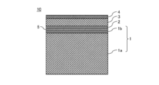
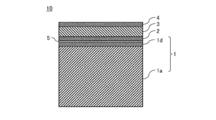
- the laminated body (laminated substrate) 10 (hereinafter, also referred to as the piezoelectric laminated body 10) having the piezoelectric film according to the present embodiment is on the substrate 1 and the substrate 1.
- the substrate 1 is a single crystal silicon (Si) substrate 1a on which a surface oxide film (SiO 2 film) 1b such as a thermal oxide film or a CVD (Chemical Vapor Deposition) oxide film is formed, that is, a Si substrate having a surface oxide film.
- a Si substrate 1a having an insulating film 1d formed of an insulating material other than SiO 2 on its surface can also be used.
- a Si substrate 1a in which a Si (100) surface or a Si (111) surface is exposed on the surface that is, a Si substrate having no surface oxide film 1b or insulating film 1d can also be used.
- the substrate 1 is formed of a metal material such as an SOI (Silicon On Insulator) substrate, a quartz glass (SiO 2 ) substrate, a gallium arsenide (GaAs) substrate, a sapphire (Al 2 O 3 ) substrate, and stainless steel (SUS). It is also possible to use a metal substrate.
- the thickness of the single crystal Si substrate 1a can be, for example, 300 ⁇ m or more and 1000 ⁇ m or less, and the thickness of the surface oxide film 1b can be, for example, 1 nm or more and 4000 nm or less.
- the oxide film 5 is a film containing zinc and oxygen as main elements.
- the oxide film 5 can be formed by using, for example, zinc oxide.
- the (0001) plane of the crystal constituting the ZnO film 5 is parallel to the main surface of the substrate 1.
- the (0001) plane is inclined at an angle within ⁇ 5 ° with respect to the main surface of the substrate 1.
- the crystals constituting the ZnO film 5 are preferentially oriented in the (0001) plane orientation.
- the fact that the crystals constituting the ZnO film 5 are preferentially oriented in the (0001) plane orientation is caused by the crystals oriented in the (0002) plane orientation in the X-ray diffraction pattern obtained by the X-ray diffraction (XRD) measurement. It means that the diffraction peak is in the highest state. That is, it is preferable that the surface of the ZnO film 5 (the surface serving as the base of the lower electrode film 2) is mainly composed of the ZnO (0001) surface.
- the ZnO film 5 can be formed by using a sputtering method, a vapor deposition method, or the like.
- the ZnO film 5 functions as an adhesion film that enhances the adhesion between the substrate 1 and the lower electrode film 2 described later.
- the thickness of the ZnO film 5 can be, for example, 1 nm or more, preferably 2 nm or more.
- the ZnO film 5 can be reliably functioned as the above-mentioned adhesion film, and when the thickness is 2 nm or more, the ZnO film 5 can be used as the above-mentioned adhesion film. It will be possible to make it function more reliably. In addition, it is possible to surely enhance the orientation of the KNN film 3 described later.
- the upper limit of the thickness of the ZnO film 5 is not particularly limited, but from the viewpoint of suppressing a decrease in the productivity of the piezoelectric laminate 10, the thickness of the ZnO film 5 is, for example, 50 nm or less, preferably 20 nm or less, more preferably 10 nm or less. Can be.
- the lower electrode film 2 can be formed by using, for example, platinum (Pt).
- the lower electrode film 2 is a polycrystalline film or a single crystal film (hereinafter, these are also referred to as Pt films).
- the (111) plane of the crystal constituting the Pt film is parallel to the main surface of the substrate 1, and the ((111) plane) is inclined at an angle within ⁇ 5 ° with respect to the main surface of the substrate 1. It is preferable that there are many crystals), that is, the crystals constituting the Pt film are preferentially oriented in the (111) plane orientation.
- the crystal constituting the Pt film is preferentially oriented in the (111) plane orientation, that is, the diffraction peak caused by the crystal oriented in the (111) plane orientation is the highest in the X-ray diffraction pattern obtained by the XRD measurement. Means that it is in. That is, it is preferable that the surface of the lower electrode film 2 (the surface serving as the base of the piezoelectric film 3) is mainly composed of the Pt (111) surface.
- the lower electrode film 2 can be formed by using a sputtering method, a vapor deposition method, or the like.
- the lower electrode film 2 (Pt film) on the ZnO film 5 whose surface is mainly composed of the ZnO (0001) surface, the surface is mainly composed of the Pt (111) surface.
- the lower electrode film 2 can be easily obtained.
- the lower electrode film 2 can also be formed by using various metals such as gold (Au), ruthenium (Ru), and iridium (Ir), and alloys containing these as main components.
- the thickness of the lower electrode film 2 can be, for example, 100 nm or more and 400 nm or less.
- the piezoelectric film 3 is, for example, an alkaline niobium oxide film containing potassium (K), sodium (Na), niobium (Nb), and oxygen (O).
- the piezoelectric film 3 can be formed by using sodium niobate potassium (KNN).
- the piezoelectric film 3 is a KNN polycrystalline film (hereinafter, also referred to as KNN film 3).
- the crystal structure of KNN has a perovskite structure, that is, the KNN film 3 has a perovskite structure.
- the KNN film 3 can be formed by using a method such as a sputtering method, a PLD (Pulsed Laser Deposition) method, or a sol-gel method.
- the thickness of the KNN film 3 can be, for example, 0.5 ⁇ m or more and 5 ⁇ m or less.
- the crystals constituting the KNN film 3 are oriented in the (001) plane direction with respect to the main surface of the substrate 1 (Si substrate 1a when the substrate 1 is, for example, a Si substrate 1a having a surface oxide film 1b or an insulating film 1d). It is preferably preferentially oriented. That is, it is preferable that the surface of the KNN film 3 (the surface serving as the base of the upper electrode film 4) is mainly composed of the KNN (001) surface. For example, by directly forming the KNN film 3 on the Pt film (lower electrode film 2) whose surface is mainly composed of Pt (111) surfaces, the surface is mainly composed of KNN (001) surfaces. The KNN film 3 can be easily obtained.
- the fact that the crystals constituting the KNN film 3 are oriented in the (001) plane orientation means that the (001) planes of the crystals constituting the KNN film 3 are parallel to the main surface of the substrate 1.
- the fact that the (001) plane of the crystal constituting the KNN film 3 is parallel to the main surface of the substrate 1 is other than the case where the (001) plane is completely parallel to the main surface of the substrate 1.
- (001) may be inclined within ⁇ 5 °, preferably within ⁇ 3 °, with respect to the main surface of the substrate 1.
- the fact that the crystals constituting the KNN film 3 are preferentially oriented in the (001) plane direction means that there are many crystals in which the (001) plane is parallel to the main plane of the substrate 1.
- the orientation ratio of the crystals constituting the KNN film 3 in the (001) plane orientation (hereinafter, also referred to as "alignment ratio of the KNN film 3" is preferably, for example, 80% or more, and is, for example, 90% or more. Is more preferable.
- Equation 1 and the "diffraction peak of the (001) plane" in the present specification refer to (001) of the crystals constituting the KNN film 3 in the X-ray diffraction pattern obtained by XRD measurement with respect to the KNN film 3.
- Diffraction peak caused by a crystal oriented in a plane orientation (that is, a crystal whose (001) plane is parallel to the main plane of the substrate 1), and a peak in which 2 ⁇ appears in the range of 20 ° or more and 23 ° or less. Is.
- Equation 1 and the "diffraction peak of the (110) plane" in the present specification are among the crystals constituting the KNN film 3 in the X-ray diffraction pattern obtained by the XRD measurement with respect to the KNN film 3. It is a diffraction peak caused by a crystal oriented in the (110) plane orientation (that is, a crystal in which the (110) plane is parallel to the main plane of the substrate 1), and 2 ⁇ is within the range of 30 ° or more and 33 ° or less. It is the peak that appears.
- the boundary between the crystals constituting the KNN film 3, that is, the grain boundaries existing in the KNN film 3 penetrate in the thickness direction of the KNN film 3.
- the grain boundaries penetrating in the thickness direction of the KNN film 3 are larger than the grain boundaries not penetrating in the thickness direction of the KNN film 3.
- the KNN film 3 contains elements other than K, Na, Nb, and O such as copper (Cu), manganese (Mn), lithium (Li), tantalum (Ta), and antimony (Sb), for example, 5 at% or less (described above). When a plurality of elements are added, the total concentration may be contained within the range of 5 at% or less).
- the upper electrode film 4 can be formed by using, for example, various metals such as Pt, Au, aluminum (Al), and Cu, or alloys thereof.
- the upper electrode film 4 can be formed by using a method such as a sputtering method, a vapor deposition method, a plating method, or a metal paste method.
- the upper electrode film 4 does not have a great influence on the crystal structure of the KNN film 3 like the lower electrode film 2. Therefore, the material, crystal structure, and film forming method of the upper electrode film 4 are not particularly limited.
- an adhesion layer containing iridium oxide (IrO 2 ) or the like as a main component may be provided.
- the thickness of the upper electrode film 4 can be, for example, 100 nm or more and 5000 nm or less, and when the adhesion layer is provided, the thickness of the adhesion layer can be, for example, 1 nm or more and 200 nm or less.
- a film containing Ti as an adhesive film (hereinafter, also simply referred to as “adhesive film”) between the substrate 1 and the lower electrode film 2 to enhance the adhesion between them.
- a ZnO film 5 is provided instead of (for example, a Ti film).
- Zinc oxide (ZnO) is less likely to diffuse than the Ti element, and hardly diffuses to the KNN film 3 through the lower electrode film 2. Therefore, the above-mentioned problems that occur when a Ti film is provided as an adhesion film, for example. Does not occur. Further, since the Zn element is less active than the Ti element, even if it diffuses to the KNN film 3, it is difficult to capture the O element in the KNN film 3 and it is difficult to cause oxygen defects in the KNN film 3. ..
- the ZnO film 5 since the ZnO film 5 is provided, it is possible to increase the number of KNN crystals whose (001) plane is parallel to the main plane of the substrate 1 as compared with the case where the Ti film is provided. That is, it is possible to reduce the number of KNN crystals whose (001) plane is inclined at a predetermined angle with respect to the main plane of the substrate 1. Further, even when the (001) plane of the KNN crystal is tilted at a predetermined angle with respect to the main plane of the substrate 1, the tilt angle can be reduced.
- the diffraction peak on the (001) plane becomes a sharp peak with a narrower half-value width than when the Ti film is provided, and the diffraction peak on the (001) plane.
- the strength increases.
- the provision of the ZnO film 5 makes it possible to set the maximum intensity of the diffraction peak on the (001) plane to 1000 cps or more and 1400 cps or less, preferably 1100 cps or more and 1350 cps or less.
- the number of KNN crystals whose (001) plane is inclined at a predetermined angle with respect to the main surface of the substrate 1 is larger than that when the ZnO film 5 is provided. , The tilt angle also increases. As a result, the diffraction peak on the (001) plane becomes a peak with a wide half-value width, and the peak intensity becomes low. In this case, the maximum intensity of the diffraction peak on the (001) plane is, for example, about 600 cps to 900 cps.
- the ZnO film 5 it is possible to obtain the KNN film 3 having both a high orientation rate and a low relative permittivity. This is because the ZnO film 5 is provided, so that the KNN film 3 maintains the high orientation rate as described above even if the film formation temperature of the KNN film 3 is lowered (for example, even if it is 500 ° C. or lower). It turned out. This is a new finding found for the first time by the inventor and others. Since the ZnO film 5 is provided in this way, the KNN film 3 can be formed at a low temperature without lowering the orientation (orientation ratio) of the KNN film 3, so that the KNN film 3 has a low dielectric constant. It is also possible to make a thin film.
- r can be, for example, 250 or more and 300 or less, preferably 250 or more and less than 300, and more preferably 250 or more and 270 or less.
- the film forming temperature of the KNN film 3 is lowered (for example, set to 500 ° C. or lower), the orientation of the KNN film 3 is lowered. Therefore, when the Ti film is provided, it is necessary to form the KNN film 3 at a high temperature (for example, over 500 ° C.) in order to prevent the orientation of the KNN film 3 from deteriorating, and as a result, the KNN film 3 needs to be formed. Dielectric constant becomes high. In this case, the relative permittivity of the KNN film 3 is, for example, about 300 to 500.
- the diffraction peak intensity of the KNN film 3, for example, the (001) plane, which has both good orientation and a low dielectric constant can be obtained without causing the above-mentioned problems. It is also possible to obtain a KNN film 3 having a high and low dielectric constant.
- FIG. 3 shows a schematic configuration diagram of a device module 30 (hereinafter, also referred to as a piezoelectric device module 30) having a KNN film 3 in the present disclosure.
- the piezoelectric device module 30 includes an element (device) 20 (element 20 having a KNN film 3, hereinafter also referred to as a piezoelectric element 20) obtained by molding the above-mentioned piezoelectric laminate 10 into a predetermined shape, and a piezoelectric element 20. It is provided with at least a voltage application unit 11a or a voltage detection unit 11b connected to the device.
- the voltage application unit 11a is a means for applying a voltage between the lower electrode film 2 and the upper electrode film 4 (between the electrodes)
- the voltage detection unit 11b is a means for applying the voltage between the lower electrode film 2 and the upper electrode film 4. It is a means for detecting the voltage generated between the electrodes (between the electrodes).
- various known means can be used as the voltage application unit 11a and the voltage detection unit 11b.
- the piezoelectric element 20 By connecting the voltage application unit 11a between the lower electrode film 2 and the upper electrode film 4 of the piezoelectric element 20, the piezoelectric element 20 can function as an actuator.
- the KNN film 3 can be deformed by applying a voltage between the lower electrode film 2 and the upper electrode film 4 by the voltage applying portion 11a.
- various members connected to the piezoelectric element 20 can be operated.
- examples of the use of the piezoelectric element 20 include a head for an inkjet printer, a MEMS mirror for a scanner, a vibrator for an ultrasonic generator, and the like.
- the piezoelectric element 20 can function as a sensor.
- a voltage is generated between the lower electrode film 2 and the upper electrode film 4 due to the deformation.
- the magnitude of the physical quantity applied to the KNN film 3 can be measured.
- applications of the piezoelectric element 20 include, for example, an angular velocity sensor, an ultrasonic sensor, a pressure sensor, an acceleration sensor, and the like.
- the piezoelectric laminate 10 is provided with the ZnO film 5 instead of the Ti film as the adhesion film, the vicinity of the interface between the KNN film 3 and the lower electrode film 2 in the KNN film 3 in particular. There are few oxygen defects present in. As a result, the piezoelectric element 20 obtained by processing the piezoelectric laminate 10 is less likely to undergo dielectric breakdown even when a positive voltage is applied.
- a substrate 1 is prepared, and a ZnO film 5 is formed on one of the main surfaces of the substrate 1 by, for example, a sputtering method.
- a sputtering method For example, using a target material made of zinc oxide, the atmosphere of a mixed gas of argon (Ar) gas and oxygen (O 2 ) gas (hereinafter, also referred to as “Ar / O 2 mixed gas atmosphere”) is obtained by the RF sputtering method.
- Ar argon
- O 2 oxygen
- the following conditions are exemplified as the conditions for forming the ZnO film 5.
- the film forming time of the ZnO film 5 can be appropriately set according to the thickness of the ZnO film 5.
- the film-forming rate can be, for example, the rate at which a ZnO film having a thickness of 2.5 nm is formed in 30 seconds.
- Atmosphere 100 W or higher and 500 W or lower, preferably 200 W or higher and 400 W or lower
- Atmosphere Ar / O 2 mixture Gas atmosphere
- Atmospheric pressure 0.1 Pa or more and 0.5 Pa or less, preferably 0.2 Pa or more and 0.4 Pa or less
- the crystals constituting the ZnO film 5 can be preferentially oriented in the (0001) plane orientation. That is, by forming the ZnO film 5 in a state where the substrate 1 is heated, it is possible to obtain the ZnO film 5 having high orientation. Further, by forming the ZnO film 5 under a temperature condition of, for example, 300 ° C. or higher, the orientation of the ZnO film 5 can be further enhanced. Further, by forming the ZnO film 5 under a temperature condition of, for example, 500 ° C. or higher, the orientation of the ZnO film 5 can be further enhanced.
- the film forming temperature of the ZnO film 5 is preferably 700 ° C. or lower.
- a lower electrode film 2 (for example, a Pt film) is formed on the ZnO film 5 in which the crystals are preferentially oriented in the (0001) plane direction, for example, by a sputtering method.
- Atmosphere Ar gas atmosphere
- Atmospheric pressure 0.1 Pa or more and 0.5 Pa or less, preferably 0.2 Pa or more and 0.4 Pa or less
- the crystals constituting the Pt film can be preferentially oriented in the (111) plane orientation. That is, by forming a Pt film in a state where the substrate 1 is heated, it is possible to obtain a Pt film having high orientation. Further, by forming the Pt film under a temperature condition of, for example, 300 ° C. or higher, the orientation of the Pt film can be further enhanced. Further, by forming the Pt film under a temperature condition of, for example, 500 ° C. or higher, the orientation of the Pt film can be further enhanced.
- the film formation temperature of the Pt film As described above, the higher the film formation temperature of the Pt film, the higher the orientation of the Pt film tends to be. However, even if the film formation temperature of the Pt film exceeds 700 ° C., the orientation of the Pt film is enhanced. While the effect has reached a plateau, it takes time to lower the temperature in the atmosphere from the film forming temperature of the Pt film to the film forming temperature of the KNN film 3 described later, and as a result, the productivity of the piezoelectric laminate 10 is increased. May decrease. Therefore, the film forming temperature of the Pt film is preferably 700 ° C. or lower.
- the KNN film 3 is formed on the Pt film in which the crystals are preferentially oriented in the (111) plane direction in advance, for example, by a sputtering method.
- the composition ratio of the KNN film 3 can be adjusted, for example, by controlling the composition of the target material used during sputtering film formation.
- the target material can be produced by mixing K 2 CO 3 powder, Na 2 CO 3 powder, Nb 2 O 5 powder and the like and firing them.
- the composition of the target material can be controlled by adjusting the mixing ratio of K 2 CO 3 powder, Na 2 CO 3 powder, Nb 2 O 5 powder and the like.
- the material may be used.
- the film forming time can be appropriately set according to the thickness of the KNN film 3.
- Discharge power 2000 W or more and 2400 W or less, preferably 2100 W or more and 2300 W or less
- Atmosphere Ar gas + oxygen (O 2 ) gas atmosphere
- Atmospheric pressure 0.2 Pa or more and 0.5 Pa or less, preferably 0.2 Pa or more and 0.4 Pa or less
- O 2 Partial pressure of Ar gas to gas (Ar / O 2 partial pressure ratio): 30/1 to 20/1, preferably 27/1 to 22/1
- Film formation temperature 430 ° C or more and 700 ° C or less
- Film formation speed 0.5 ⁇ m / hr or more and 2 ⁇ m / hr or less, preferably 0.75 ⁇ m / hr or more and 1.5 ⁇ m / hr or less
- the crystals constituting the KNN film 3 are prioritized in the (001) plane orientation. It can be oriented.
- the film is formed on the lower electrode film 2. It is possible to increase the orientation of the KNN film 3 to be formed. As a result, for example, 80% or more of the crystals constituting the KNN film 3 can be oriented in the (001) plane orientation. That is, it is possible to obtain the KNN film 3 having the above-mentioned orientation ratio of, for example, 80% or more.
- the film-forming temperature of the lower electrode film 2 can be made lower than the film-forming temperature of the ZnO film 5.
- the ZnO film 5 and the lower electrode film 2 under temperature conditions of 300 ° C. or higher, for example, 80% or more of the crystals constituting the KNN film 3 are oriented in the (001) plane orientation. It is possible to reliably orient the film. That is, it is possible to reliably obtain the KNN film 3 having the above-mentioned orientation ratio of, for example, 80% or more.
- the ZnO film 5 and the lower electrode film 2 under temperature conditions of 500 ° C. or higher, for example, 85% or more, preferably 90% or more of the crystals constituting the KNN film 3 are formed.
- the film forming temperature of the KNN film 3 is preferably 500 ° C. or higher and 700 ° C. or lower, and more preferably 540 ° C. or higher and 700 ° C. or lower. This makes it possible to surely increase the withstand voltage of the KNN film 3 when a positive voltage is applied.
- the film forming temperature of the KNN film 3 is preferably 430 ° C. or higher and 500 ° C. or lower, and more preferably 440 ° C. or higher and 470 ° C. or lower. Since the ZnO film 5 is provided, it is possible to make the KNN film 3 a highly oriented film even if the film forming temperature of the KNN film 3 is lowered in this way. Further, by forming the KNN film 3 at such a low temperature, the KNN film 3 can be made into a film having a low dielectric constant. That is, it is possible to obtain a KNN film 3 having both a high orientation rate and a low dielectric constant that can be suitably used as a sensor.
- the upper electrode film 4 is formed on the KNN film 3 by, for example, a sputtering method.
- the conditions for forming the upper electrode film 4 can be the same as the conditions for forming the lower electrode film 2 described above.
- the ZnO film 5, the lower electrode film 2 (Pt film), the KNN film 3, and the upper electrode film 4 are formed on the substrate 1 in this order, thereby forming a piezoelectric film as shown in FIG.
- the laminated body 10 is obtained.
- the obtained piezoelectric laminate 10 is molded into a predetermined shape by etching or the like (microfabrication is performed on a predetermined pattern).
- the piezoelectric element 20 as shown in FIG. 3 is obtained, and the piezoelectric device module 30 can be obtained by connecting the voltage application unit 11a or the voltage detection unit 11b to the piezoelectric element 20.
- the etching method for example, a dry etching method such as reactive ion etching or a wet etching method using a predetermined etching solution can be used.
- a photoresist pattern as an etching mask for dry etching is formed on the piezoelectric laminate 10 (for example, the upper electrode film 4) by a photolithography process or the like.
- a noble metal film such as a chromium (Cr) film, a nickel (Ni) film, a platinum (Pt) film, and a Ti film may be formed by a sputtering method.
- dry etching is performed on the piezoelectric laminate 10 (upper electrode film 4, KNN film 3, etc.) using a gas containing a halogen element as the etching gas.
- the halogen element includes chlorine (Cl), fluorine (F) and the like.
- the gas containing a halogen element BCl 3 gas, SiC 4 gas, chlorine (Cl 2 ) gas, CF 4 gas, C 4 F 8 gas and the like can be used.
- a silicon oxide (SiO x ) film or the like as an etching mask for wet etching is formed on the piezoelectric laminate 10 (for example, the upper electrode film 4). Then, for example, the piezoelectric laminate 10 is immersed in an etching solution containing an alkaline aqueous solution of a chelating agent and not containing hydrofluoric acid, and wet etching is performed on the piezoelectric laminate 10 (upper electrode film 4, KNN film 3, etc.).
- etching solution containing an alkaline aqueous solution of a chelating agent and not containing hydrofluoric acid an etching solution obtained by mixing ethylenediaminetetraacetic acid as a chelating agent, aqueous ammonia, and aqueous hydrogen peroxide can be used.
- the Ti film is provided by providing the ZnO film 5 instead of the film containing Ti (for example, the Ti film) as the adhesion film that adheres the substrate 1 and the lower electrode film 2 to each other. Adhesion of the same level or higher can be maintained.
- the adhesive film is composed of the ZnO film 5, so that the element that diffuses into the KNN film 3 is more difficult than when the adhesive film is composed of the Ti film. Can be reduced. This makes it possible to suppress the generation of oxygen defects in the KNN film 3, especially in the vicinity of the interface between the KNN film 3 and the lower electrode film 2.
- the withstand voltage of the KNN film 3 when a positive voltage is applied can be increased, and the deterioration of the insulating property when a positive voltage is applied can be avoided. That is, in the piezoelectric element 20 obtained by processing the above-mentioned piezoelectric laminated body 10, dielectric breakdown is less likely to occur even when a positive voltage is applied.
- an electric field of 300 kV / cm (from the upper electrode film 4 to the lower part) between the lower electrode film 2 and the upper electrode film 4 in a state where the piezoelectric laminate 10 (piezoelectric element 20) is heated to a temperature of 200 ° C.
- a high acceleration life test (Highly Accelerated Life Test, abbreviated as HALT) is performed in which a positive voltage is applied to the upper electrode film 4 while the lower electrode film 2 is grounded so as to generate an electric field toward the electrode film 2.
- HALT Highly Accelerated Life Test
- the time from the start of voltage application to the destruction of the insulation of the KNN film 3 can be set to 1500 seconds or more.
- the KNN film 3 has undergone dielectric breakdown when the leakage current density flowing through the KNN film 3 exceeds 30 mA / cm 2.
- a film containing no Ti containing tantalum (Ta), tantalum oxide (Ta 2 O 5 ), nickel (Ni) or the like as a main component, or a titanium oxide (TiO 2 ) film may be formed. Proposed.
- these films have a problem that the adhesion is clearly weaker than that of the Ti film and the ZnO film 5.
- the ZnO film 5 is provided as the adhesion film, it is possible to maintain the adhesion equal to or higher than that of the Ti film.
- the KNN film 3 can be made into a film having a high diffraction peak intensity on the (001) plane.
- the maximum intensity of the diffraction peak on the (001) plane can be 1000 cps or more and 1400 cps or less.
- the ZnO film 5 is provided as an adhesion film for bringing the substrate 1 and the lower electrode film 2 into close contact with each other, so that the KNN film 3 has both a high orientation rate and a low dielectric constant. It becomes possible. This is because the provision of the ZnO film 5 makes it possible to form the KNN film 3 at a low temperature without lowering the orientation ratio of the KNN film 3. Since the KNN film 3 can be formed at a low temperature, the KNN film 3 can be made into a film having a low dielectric constant.
- the relative permittivity of the KNN film 3 when measured by applying a voltage of -1V to + 1V with a triangular wave having a frequency of 3 kHz with the lower electrode film 2 as the ground can be set to 250 or more and 300 or less.
- the piezoelectric laminate 10 having such a KNN film 3 can be particularly suitably used for applications such as high-sensitivity sensors that require a low dielectric constant.
- the piezoelectric element 20 in which the HALT result under predetermined conditions is 1500 seconds or longer, preferably 1600 seconds or longer, when the orientation rate of the crystals constituting the KNN film 3 in the (001) plane direction is 80% or more. Can be obtained. Further, when the orientation rate of the crystals constituting the KNN film 3 in the (001) plane direction is 90% or more, it is possible to obtain the piezoelectric element 20 in which the HALT result under predetermined conditions is 1800 seconds or more. ..
- the ZnO film 5 When the thickness of the ZnO film 5 is, for example, 1 nm or more, the ZnO film 5 can be reliably functioned as an adhesive film that adheres the substrate 1 and the lower electrode film 2 to each other. As a result, it is possible to reliably prevent the lower electrode film 2 from peeling off from the substrate 1 during the manufacturing process of the piezoelectric laminate 10, the piezoelectric element 20, and the piezoelectric device module 30 or when a voltage is applied. Further, when the thickness of the ZnO film 5 is, for example, 1 nm or more, the orientation of the KNN film 3 can be further enhanced.
- the lower electrode film 2 can be formed by using a metal oxide such as strontium ruthenate (SrRuO 3 , abbreviated as SRO) or lanthanum nickelate (LaNiO 3, abbreviated as LNO).
- a metal oxide such as strontium ruthenate (SrRuO 3 , abbreviated as SRO) or lanthanum nickelate (LaNiO 3, abbreviated as LNO).
- SRO strontium ruthenate
- LaNiO 3 lanthanum nickelate
- LNO lanthanum nickelate
- the lower electrode film 2 by forming the lower electrode film 2 under the same temperature conditions as in the above aspect, the lower electrode film 2 preferentially oriented in the (001) plane direction can be formed.
- the lower electrode film 2 may be a single-layer film formed by using the above-mentioned various metals or metal oxides, or on a metal film and a metal film formed by using a metal such as Pt. It may be a laminate with a provided film made of SRO, a laminate made of a metal film and a film made of LNO provided on the metal film, or the like. Also in this aspect, the same effect as the above-mentioned aspect can be obtained.
- the piezoelectric element 20 produced by using the piezoelectric laminate 10 can be applied to a desired application such as a sensor or an actuator, as long as the piezoelectric laminate 10 can be applied.
- the substrate 1 may be removed from 10.
- a Si substrate having a surface oriented in (100) plane orientation, a thickness of 610 ⁇ m, a diameter of 6 inches, and a thermal oxide film (SiO 2 film) having a thickness of 200 nm formed on the surface is prepared. did. Then, on this substrate (on the thermal oxide film), the first adhesive film, the Pt film as the lower electrode film (thickness: 200 nm), the KNN film as the piezoelectric film (thickness: 2 ⁇ m), and the second adhesive film. RuO 2 film (thickness: 10 nm) and Pt film (thickness: 100 nm) as the upper electrode film were formed in this order to prepare a piezoelectric laminate (samples 1 to 16).
- the first adhesive film is a film for adhering the substrate and the lower electrode film
- the second adhesive film is a film for adhering the KNN film and the upper electrode film.
- a ZnO film or a Ti film was formed as the first adhesion film. Further, the thickness of the first adhesive film was changed within the range of 0.5 nm or more and 50 nm or less.
- the first adhesion film (ZnO film or Ti film) was formed by the RF magnetron sputtering method.
- the conditions for forming the first adhesive film were as follows. Among the following conditions, the film forming temperature means the temperature of the heater of the sputtering apparatus (the same applies to the conditions of other films). Further, the film forming temperature of room temperature means that the first adhesive film is formed in a non-heated state. Further, the film forming time was appropriately changed according to the thickness of the first adhesive film to be formed.
- Film formation temperature Predetermined temperature within the range of room temperature (for example, 28 ° C) or more and 700 ° C or less Atmosphere of mixed gas of Ar gas and O 2 gas Introduced gas: Ar gas: 100 cc, O 2 gas: 10 cc Atmospheric pressure: 0.2Pa Discharge power: 300W Film formation rate: The rate at which the first adhesive film with a thickness of 2.5 nm is formed in 30 seconds.
- the lower electrode film and the upper electrode film were formed by the RF magnetron sputtering method.
- the conditions for forming the lower electrode film and the upper electrode film were as follows. Film formation temperature: 300 ° C Discharge power: 1200W Introduced gas: Ar gas Atmospheric pressure: 0.3Pa Film formation time: 5 minutes
- the KNN film was formed by the RF magnetron sputtering method.
- a Na x ) NbO 3 sintered body was used.
- K 2 CO 3 powder, Na 2 CO 3 powder, and Nb 2 O 5 powder were mixed for 24 hours using a ball mill, calcined at 850 ° C. for 10 hours, and then pulverized again with a ball mill. , 200 MPa, and then calcined at 1080 ° C. to produce.
- the composition of the target material is controlled by adjusting the mixing ratio of K 2 CO 3 powder, Na 2 CO 3 powder, and Nb 2 O 5 powder, and EDX (energy dispersive X-ray spectroscopic analysis) is performed before the film formation process. ).
- the conditions for forming the KNN film were as follows. Film formation temperature: 550 ° C Discharge power: 2200W Introduced gas: Mixed gas atmosphere pressure of Ar gas and O 2 gas: 0.3Pa The partial pressure ratio of Ar gas to the O 2 gas (Ar gas partial pressure / O 2 gas partial pressure): 25/1 Film formation speed: 1 ⁇ m / hr
- the orientation of the KNN film was evaluated by measuring the orientation rate of the crystals constituting the KNN film in the (001) plane orientation.
- the orientation ratio of the KNN film was measured by XRD for each sample to obtain an X-ray diffraction pattern.
- the conditions for XRD measurement were as follows.
- Output current 22mA KNN film thickness: 2um
- Equation 1 Calculated according to the above (Equation 1) based on the peak intensity of the obtained diffraction pattern.
- the calculation results of the orientation rate are as shown in Table 1 above.
- the orientation of the KNN film can be enhanced by forming the ZnO film and the lower electrode film at a temperature of 200 ° C. or higher, respectively. It was confirmed that a KNN film having the above-mentioned orientation ratio of 80% or more could be obtained. If the ZnO film and the lower electrode film are formed in a non-heated state or at a temperature of less than 200 ° C., the orientation of the KNN film cannot be improved and the orientation rate becomes less than 80%. I was able to confirm that.
- the orientation of the KNN film is higher than that in the case of forming a film at a temperature of 200 ° C. It was confirmed that the sex could be further enhanced.
- the orientation of the KNN film is further improved by forming the ZnO film and the lower electrode film as the first adhesion film at a temperature of 500 ° C. or higher (for example, 500 ° C., 700 ° C.). It was confirmed that the KNN film having the above-mentioned orientation ratio of 90% or more could be obtained.
- the orientation rate of the KNN film is less than 80% even when the film formation temperature of the Ti film and the lower electrode film is 500 ° C. I was able to confirm that there were cases.
- the thickness of the ZnO film as the first adhesion film is 1 nm or more, the adhesion force equal to or higher than that when the Ti film is provided as the first adhesion film is maintained. I was able to confirm that it was possible.
- the thickness of the ZnO film as the first adhesion film was less than 1 nm (for example, 0.5 nm), it was confirmed that the adhesion was weak and there was a part where the lower electrode film was peeled off from the substrate. Further, it was confirmed that even when a Ti film having a thickness of 1 nm was provided as the first adhesive film, there was a part where the lower electrode film was peeled off from the substrate.
- the evaluation of the insulation property when a positive voltage is applied is to evaluate the electric field of 300 kV / cm between the lower electrode film and the upper electrode film in a state where the temperature of each piezoelectric laminate (each sample) is heated to 200 ° C.
- HALT is performed in which a positive voltage is applied to the upper electrode film while the lower electrode film is grounded so as to generate an electric field from the upper electrode film to the lower electrode film
- the KNN film is insulated from the start of voltage application. This was done by measuring the time to destruction.
- the leakage current density flowing through the KNN film exceeded 30 mA / cm 2 , it was considered that the KNN film had undergone dielectric breakdown.
- HALT life The time until the KNN film measured by HALT under the above conditions reaches dielectric breakdown is defined as "HALT life”.
- HALT lifetime of each sample is as shown in Table 1. These HALT lifetimes (measurement results) are the average of the values measured at 7 points within 0.5 mm ⁇ for each sample. The description of "1800 seconds or more" in Table 1 means that dielectric breakdown did not occur even after 1800 seconds had passed from the start of voltage application.
- the orientation ratio of the KNN film is 80% or more, and the HALT life is 1500 seconds or longer. It was confirmed that a piezoelectric laminate (KNN film) was obtained.
- the orientation rate of the KNN film is 90% and the HALT life is 1800 seconds or longer. It was confirmed that a laminated body was obtained.
- the thickness of the ZnO film is less than 1 nm (for example, 0.5 nm)
- the alignment rate of the KNN film is 85% or more by forming the ZnO film and the lower electrode film under the temperature condition of 500 ° C. or higher. It was confirmed that a piezoelectric laminate having a HALT life of 1700 seconds or more could be obtained.
- the orientation ratio of the KNN film is 90% or more and the HALT life is long even if the ZnO film and the lower electrode film are formed under a temperature condition of 500 ° C. or higher. It has been confirmed that it is difficult to obtain a piezoelectric laminate that takes 1800 seconds or more.
- the thickness of the ZnO film or the Ti film as the first adhesion film was as shown in Table 2 below, and the film formation temperature of the first adhesion film was 500 ° C. Further, the film forming temperature of the lower electrode film was set to 500 ° C. Further, the film forming temperature of the KNN film was set to 460 ° C. Other methods and conditions were the same as those of Samples 1 to 16 described above.
- the measurement of the orientation ratio of the crystals constituting the KNN film in the (001) plane orientation was performed by the same method and conditions as the measurement of the orientation ratio of the samples 1 to 16.
- the diffraction peak intensity of the (001) plane of the KNN film was measured by XRD for each of the samples 17 to 21 to obtain an X-ray diffraction pattern (2 ⁇ / ⁇ ), and in the obtained X-ray diffraction pattern, 2 ⁇ .
- the conditions for XRD measurement were as follows.
- Output current 22mA KNN film thickness: 2um
- the relative permittivity was measured by applying a voltage of -1V to + 1V to the upper electrode film 4 with a triangular wave having a frequency of 3 kHz with the lower electrode film 2 as the ground.
- the measurement results of the orientation rate, diffraction peak intensity, and relative permittivity are as shown in Table 2 above.
- the “001 intensity” in Table 2 means the diffraction peak intensity of the (001) plane of the KNN film.
- the ZnO film is provided as the first adhesion film, the orientation of the KNN film is lowered even when the film formation temperature of the KNN film is low (500 ° C. or lower, for example, 460 ° C.). I was able to confirm that there was nothing. That is, by providing the ZnO film, even if the KNN film is formed at a low temperature, the maximum intensity of the diffraction peak of the (001) plane can be 1000 cps or more and 1400 cps or less, preferably 1100 cps or more and 1350 cps or less. Was confirmed.
- the relative permittivity of the KNN film can be lowered by forming the KNN film at a low temperature. That is, it was confirmed that the relative permittivity can be 250 or more and 300 or less, preferably 250 or more and less than 300, and more preferably 250 or more and 270 or less.
- the KNN film can be formed at a low temperature without deteriorating the orientation of the KNN film by providing the ZnO film. That is, it was confirmed that the KNN film having both a high orientation rate and a low dielectric constant can be obtained by providing the ZnO film.
- Such a KNN film can be particularly suitably used for applications of high-sensitivity sensors.
- Appendix 2 The piezoelectric laminate according to Appendix 1, preferably.
- the orientation ratio of the crystals constituting the piezoelectric film in the (001) plane direction is 80% or more.
- Appendix 3 The piezoelectric laminate according to Appendix 1 or 2, preferably.
- the upper electrode film is provided on the piezoelectric film so as to generate an electric field of 300 kV / cm between the upper electrode film, which is a film different from the electrode film, and the electrode film.
- the time from the start of voltage application until the leakage current density flowing through the piezoelectric film exceeds 30 mA / cm 2 is 1500 seconds or more, preferably 1600 seconds or more.
- the piezoelectric laminate according to Appendix 4 preferably.
- the upper electrode film is provided on the piezoelectric film at a temperature of 200 ° C., and an electric field of 300 kV / cm is generated between the upper electrode film, which is an electrode film different from the electrode film, and the electrode film.
- the time from the start of voltage application until the leakage current density flowing through the piezoelectric film exceeds 30 mA / cm 2 is 1800 seconds or more.
- a positive voltage is applied to the upper electrode film so as to generate an electric field of 300 kV / cm between the upper electrode film and the lower electrode film at a temperature of 200 ° C.
- the piezoelectricity is applied from the start of voltage application.
- the time required for the leakage current density flowing through the film to exceed 30 mA / cm 2 is 1500 seconds or longer, preferably 1600 seconds or longer.
- (Appendix 12) The piezoelectric element or piezoelectric device module according to Appendix 9, preferably.
- the orientation rate of the crystals constituting the piezoelectric film in the (001) plane direction is 90% or more.
- Appendix 13 The piezoelectric element or piezoelectric device module according to Appendix 12, preferably.
- a positive voltage is applied to the upper electrode film so as to generate an electric field of 300 kV / cm between the upper electrode film and the lower electrode film at a temperature of 200 ° C.
- the piezoelectricity is applied from the start of voltage application. It takes 1800 seconds or more for the leakage current density flowing through the membrane to exceed 30 mA / cm 2.
- the oxide film is formed under a temperature condition of 200 ° C. or higher.
- the electrode film is formed under a temperature condition of 200 ° C. or higher.
- the crystals constituting the oxide film are preferentially oriented in the (0001) plane orientation.
- the crystals constituting the electrode film are preferentially oriented in a predetermined direction.
- the crystals constituting the electrode film are preferentially oriented in the (111) plane orientation, and a predetermined electrode film is formed.
- the crystals constituting the electrode film are preferentially oriented in the (001) plane orientation.
Abstract
This piezoelectric laminate comprises: a substrate; an oxide film formed on the substrate and containing zinc and oxygen as main elements; an electrode film formed on the oxide film; and a piezoelectric film, which is an alkaline niobium oxide film having a perovskite structure, formed on the electrode film and containing potassium, sodium, niobium, and oxygen.
Description
本開示は、圧電積層体、圧電素子および圧電積層体の製造方法に関する。
The present disclosure relates to a piezoelectric laminate, a piezoelectric element, and a method for manufacturing a piezoelectric laminate.
圧電体は、センサ、アクチュエータ等の機能性電子部品に広く利用されている。圧電体の材料としては、鉛系材料、特に、組成式Pb(Zr1-xTix)O3で表されるPZT系の強誘電体が広く用いられている。PZT系の圧電体は鉛を含有しているため、人体への影響の懸念等から好ましくない。そこで、鉛非含有の圧電体として、カリウム、ナトリウム、ニオブ、及び酸素を含む圧電体が提案されており、このような圧電体を用いて製膜された圧電膜を有する積層体が提案されている(例えば特許文献1,2参照)。
Piezoelectrics are widely used in functional electronic components such as sensors and actuators. As the material of the piezoelectric material, a lead-based material, particularly a PZT-based ferroelectric substance represented by the composition formula Pb (Zr 1-x Ti x ) O 3 is widely used. Since the PZT-based piezoelectric material contains lead, it is not preferable because of concerns about its influence on the human body. Therefore, as a lead-free piezoelectric material, a piezoelectric material containing potassium, sodium, niobium, and oxygen has been proposed, and a laminate having a piezoelectric film formed by using such a piezoelectric material has been proposed. (See, for example, Patent Documents 1 and 2).
上述の特許技術では、圧電膜の厚さ方向に電界を印加した際、厚さ方向の一方に向かって電界を印加した場合よりも厚さ方向の他方に向かって電界を印加した場合の方が、絶縁破壊が起こりやすいことが判明した。すなわち、圧電膜の耐圧が印加する電界の向きに応じて異なる場合があることが判明した。このことは、発明者の鋭意研究によって初めて明らかとなった新規課題である。
In the above-mentioned patented technique, when an electric field is applied in the thickness direction of the piezoelectric film, it is better when the electric field is applied toward the other in the thickness direction than when the electric field is applied toward one in the thickness direction. , It turned out that dielectric breakdown is likely to occur. That is, it was found that the withstand voltage of the piezoelectric film may differ depending on the direction of the applied electric field. This is a new issue that was first revealed by the inventor's diligent research.
また、上述の特許技術では、圧電膜の誘電率を低くしようとして圧電膜の製膜温度を低くすると、圧電膜の結晶配向性が低下するという課題もあった。
Further, in the above-mentioned patented technology, there is also a problem that the crystal orientation of the piezoelectric film is lowered when the film forming temperature of the piezoelectric film is lowered in an attempt to lower the dielectric constant of the piezoelectric film.
本開示は、カリウム、ナトリウム、ニオブ、及び酸素を含む圧電膜の性能をさらに向上させることを目的とする。
The present disclosure is intended to further improve the performance of piezoelectric membranes containing potassium, sodium, niobium, and oxygen.
本開示の一態様によれば、
基板と、
前記基板上に製膜され、亜鉛および酸素を主要元素とする酸化膜と、
前記酸化膜上に製膜される電極膜と、
前記電極膜上に製膜され、カリウム、ナトリウム、ニオブ、及び酸素を含み、ペロブスカイト構造を有するアルカリニオブ酸化膜である圧電膜と、を備える圧電積層体およびその関連技術が提供される。 According to one aspect of the present disclosure
With the board
An oxide film formed on the substrate and containing zinc and oxygen as the main elements, and
The electrode film formed on the oxide film and
Provided are a piezoelectric laminate comprising a piezoelectric film formed on the electrode film, containing potassium, sodium, niobium, and oxygen, and an alkaline niobium oxide film having a perovskite structure, and a related technique thereof.
本開示によれば、カリウム、ナトリウム、ニオブ、及び酸素を含む圧電膜の性能をさらに向上させることが可能となる。
According to the present disclosure, it is possible to further improve the performance of the piezoelectric membrane containing potassium, sodium, niobium, and oxygen.
<発明者が得た知見>
基板と、基板上に製膜された下部電極膜と、下部電極膜上に製膜され、カリウム(K)、ナトリウム(Na)、ニオブ(Nb)、及び酸素(O)を含む圧電膜(KNN膜)と、KNN膜上に製膜された上部電極膜と、を有する積層体において、基板と下部電極膜との間にこれらを互いに密着させる密着膜としてチタン(Ti)を含む膜(例えば、Ti膜)が設けられることが一般的である。このような密着膜が設けられた積層体を用いて作製した圧電素子(圧電デバイスモジュール)では、負電圧印加時に比べて、正電圧印加時に絶縁破壊が起こりやすいことが判明した。ここで、本明細書における負電圧印加とは、上部電極膜側をマイナス、下部電極膜側をアースにして、上部電極膜と下部電極膜との間にKNN膜の厚さ方向の上向き(下部電極膜から上部電極膜に向かう向き)の電界が生じるように、上部電極膜に対して負電圧を印加することを意味する。また、本明細書における正電圧印加とは、上部電極膜側をプラス、下部電極膜側をアースにして、上部電極膜と下部電極膜との間にKNN膜の厚さ方向の下向き(上部電極膜から下部電極膜に向かう向き)の電界が生じるように、上部電極膜に対して正電圧を印加することを意味する。 <Findings obtained by the inventor>
A substrate, a lower electrode film formed on the substrate, and a piezoelectric film (KNN) formed on the lower electrode film and containing potassium (K), sodium (Na), niobium (Nb), and oxygen (O). In a laminate having a film) and an upper electrode film formed on a KNN film, a film containing titanium (Ti) as an adhesion film that adheres the substrate and the lower electrode film to each other (for example, (Ti film) is generally provided. It has been found that in a piezoelectric element (piezoelectric device module) manufactured by using a laminate provided with such an adhesive film, dielectric breakdown is more likely to occur when a positive voltage is applied than when a negative voltage is applied. Here, the negative voltage application in the present specification means that the upper electrode film side is negative and the lower electrode film side is ground, and the KNN film is upwardly oriented in the thickness direction between the upper electrode film and the lower electrode film (lower part). It means that a negative voltage is applied to the upper electrode film so that an electric field (in the direction from the electrode film toward the upper electrode film) is generated. Further, the positive voltage application in the present specification means that the upper electrode film side is positive and the lower electrode film side is ground, and the KNN film is located between the upper electrode film and the lower electrode film downward in the thickness direction (upper electrode). It means that a positive voltage is applied to the upper electrode film so that an electric field (in the direction from the film toward the lower electrode film) is generated.
発明者は、上記課題について鋭意研究を行った。その結果、密着膜中のTiが下部電極膜を通過してKNN膜まで拡散することがあり、このことが、正電圧印加時において絶縁破壊を引き起こす要因ではないか、との知見を得た。というのも、Tiは例えばKNN製膜時の温度環境で下部電極膜の上面(KNN膜と接する側の面)まで拡散で容易に広がる。このため、密着膜としてTiを含む膜が設けられていると、密着膜中のTiが圧電膜まで拡散して圧電膜中の酸素と結合して(圧電膜中の酸素を捕獲し)、TiOxとなる。これにより、圧電膜中、特に圧電膜と下部電極膜との間の界面近傍に酸素欠陥(酸素欠損、酸素空孔(Oxygen Vacancy))が生じてしまう。このような圧電膜を有する圧電素子(圧電デバイスモジュール)において、正電圧が印加されると、圧電膜中の酸素欠陥が、下部電極膜側に向かって圧電膜中を移動し、これにより、絶縁破壊が起こってしまう。
The inventor has conducted diligent research on the above-mentioned problems. As a result, it was found that Ti in the adhesive film may pass through the lower electrode film and diffuse to the KNN film, which may cause dielectric breakdown when a positive voltage is applied. This is because Ti easily spreads by diffusion to, for example, the upper surface of the lower electrode film (the surface on the side in contact with the KNN film) in the temperature environment during KNN film formation. For this reason, if a membrane containing Ti is provided as the adhesive film, Ti in the adhesive film diffuses to the piezoelectric film and combines with oxygen in the piezoelectric film (captures oxygen in the piezoelectric film) to cause TIO. It becomes x. As a result, oxygen defects (oxygen deficiency, oxygen vacancies) occur in the piezoelectric film, particularly in the vicinity of the interface between the piezoelectric film and the lower electrode film. In a piezoelectric element (piezoelectric device module) having such a piezoelectric film, when a positive voltage is applied, oxygen defects in the piezoelectric film move in the piezoelectric film toward the lower electrode film side, thereby insulating. Destruction will occur.
また、上記密着膜としてTi膜が設けられた積層体において、圧電膜の誘電率をより低くするために、圧電膜の製膜温度をより低くすることが試みられている。しかしながら、圧電膜の製膜温度を低くすると圧電膜の結晶の配向性が低下するという課題もあった。このため、密着膜としてTi膜が設けられた場合、圧電膜の配向性の低下を回避するためには、圧電膜を高温(例えば500℃超)で製膜する必要があり、その結果、圧電膜の誘電率を充分に低くすることができなかった。すなわち、低誘電率と高配向性とを兼ね備える圧電積層体が得られなかった。
Further, in the laminated body provided with the Ti film as the adhesion film, an attempt is made to lower the film forming temperature of the piezoelectric film in order to lower the dielectric constant of the piezoelectric film. However, there is also a problem that the orientation of the crystals of the piezoelectric film is lowered when the film forming temperature of the piezoelectric film is lowered. Therefore, when a Ti film is provided as an adhesive film, it is necessary to form the piezoelectric film at a high temperature (for example, over 500 ° C.) in order to avoid deterioration of the orientation of the piezoelectric film, and as a result, piezoelectric film is formed. The dielectric constant of the film could not be lowered sufficiently. That is, a piezoelectric laminate having both low dielectric constant and high orientation could not be obtained.
本開示は、発明者等が得た上述の知見や課題に基づいてなされたものである。
This disclosure is based on the above-mentioned findings and problems obtained by the inventors.
<本開示の一態様>
以下、本開示の一態様について図面を参照しながら説明する。 <One aspect of the present disclosure>
Hereinafter, one aspect of the present disclosure will be described with reference to the drawings.
以下、本開示の一態様について図面を参照しながら説明する。 <One aspect of the present disclosure>
Hereinafter, one aspect of the present disclosure will be described with reference to the drawings.
(1)圧電積層体の構成
図1に示すように、本実施形態にかかる圧電膜を有する積層体(積層基板)10(以下、圧電積層体10とも称する)は、基板1と、基板1上に製膜された酸化膜5と、酸化膜5上に製膜された下部電極膜2と、下部電極膜2上に製膜された圧電膜(圧電薄膜)3と、圧電膜3上に製膜された上部電極膜4と、を備えている。 (1) Configuration of the piezoelectric laminated body As shown in FIG. 1, the laminated body (laminated substrate) 10 (hereinafter, also referred to as the piezoelectric laminated body 10) having the piezoelectric film according to the present embodiment is on thesubstrate 1 and the substrate 1. The oxide film 5 formed on the oxide film 5, the lower electrode film 2 formed on the oxide film 5, the piezoelectric film (piezoelectric thin film) 3 formed on the lower electrode film 2, and the piezoelectric film 3 formed on the piezoelectric film 3. It includes a filmed upper electrode film 4.
図1に示すように、本実施形態にかかる圧電膜を有する積層体(積層基板)10(以下、圧電積層体10とも称する)は、基板1と、基板1上に製膜された酸化膜5と、酸化膜5上に製膜された下部電極膜2と、下部電極膜2上に製膜された圧電膜(圧電薄膜)3と、圧電膜3上に製膜された上部電極膜4と、を備えている。 (1) Configuration of the piezoelectric laminated body As shown in FIG. 1, the laminated body (laminated substrate) 10 (hereinafter, also referred to as the piezoelectric laminated body 10) having the piezoelectric film according to the present embodiment is on the
基板1としては、熱酸化膜またはCVD(Chemical Vapor Deposition)酸化膜等の表面酸化膜(SiO2膜)1bが形成された単結晶シリコン(Si)基板1a、すなわち、表面酸化膜を有するSi基板を好適に用いることができる。また、基板1としては、図2に示すように、その表面にSiO2以外の絶縁性材料により形成された絶縁膜1dを有するSi基板1aを用いることもできる。また、基板1としては、表面にSi(100)面またはSi(111)面等が露出したSi基板1a、すなわち、表面酸化膜1bまたは絶縁膜1dを有さないSi基板を用いることもできる。また、基板1としては、SOI(Silicon On Insulator)基板、石英ガラス(SiO2)基板、ガリウム砒素(GaAs)基板、サファイア(Al2O3)基板、ステンレス(SUS)等の金属材料により形成された金属基板を用いることもできる。単結晶Si基板1aの厚さは例えば300μm以上1000μm以下、表面酸化膜1bの厚さは例えば1nm以上4000nm以下とすることができる。
The substrate 1 is a single crystal silicon (Si) substrate 1a on which a surface oxide film (SiO 2 film) 1b such as a thermal oxide film or a CVD (Chemical Vapor Deposition) oxide film is formed, that is, a Si substrate having a surface oxide film. Can be preferably used. Further, as the substrate 1, as shown in FIG. 2, a Si substrate 1a having an insulating film 1d formed of an insulating material other than SiO 2 on its surface can also be used. Further, as the substrate 1, a Si substrate 1a in which a Si (100) surface or a Si (111) surface is exposed on the surface, that is, a Si substrate having no surface oxide film 1b or insulating film 1d can also be used. Further, the substrate 1 is formed of a metal material such as an SOI (Silicon On Insulator) substrate, a quartz glass (SiO 2 ) substrate, a gallium arsenide (GaAs) substrate, a sapphire (Al 2 O 3 ) substrate, and stainless steel (SUS). It is also possible to use a metal substrate. The thickness of the single crystal Si substrate 1a can be, for example, 300 μm or more and 1000 μm or less, and the thickness of the surface oxide film 1b can be, for example, 1 nm or more and 4000 nm or less.
酸化膜5は、亜鉛および酸素を主要元素とする膜である。酸化膜5は、例えば酸化亜鉛を用いて製膜することができる。酸化膜5は、多結晶膜または単結晶膜となる(以下、酸化膜5をZnO膜5とも称する)。ZnO膜5を構成するZnおよびOの組成比はZn:O=1:1の関係を満たすことが好ましいが、これに限定されるものではなく、多少のばらつきがあってもよい。ZnO膜5を構成する結晶は、その(0001)面が基板1の主面に対して平行である結晶((0001)面が基板1の主面に対して±5°以内の角度で傾斜している結晶を含む)が多いこと、すなわち、(0001)面方位に優先配向していることが好ましい。ZnO膜5を構成する結晶が(0001)面方位に優先配向しているとは、X線回折(XRD)測定により得られたX線回折パターンにおいて(0002)面方位に配向する結晶に起因する回折ピークが最も高い状態にあることを意味する。すなわち、ZnO膜5の表面(下部電極膜2の下地となる面)は、主にZnO(0001)面により構成されていることが好ましい。なお、ZnO膜5は、スパッタリング法、蒸着法等を用いて製膜することができる。ZnO膜5は、基板1と後述の下部電極膜2との間の密着性を高める密着膜として機能する。
The oxide film 5 is a film containing zinc and oxygen as main elements. The oxide film 5 can be formed by using, for example, zinc oxide. The oxide film 5 is a polycrystalline film or a single crystal film (hereinafter, the oxide film 5 is also referred to as a ZnO film 5). It is preferable that the composition ratio of Zn and O constituting the ZnO film 5 satisfies the relationship of Zn: O = 1: 1, but the composition ratio is not limited to this, and there may be some variation. The (0001) plane of the crystal constituting the ZnO film 5 is parallel to the main surface of the substrate 1. The (0001) plane is inclined at an angle within ± 5 ° with respect to the main surface of the substrate 1. It is preferable that there are many crystals), that is, they are preferentially oriented in the (0001) plane orientation. The fact that the crystals constituting the ZnO film 5 are preferentially oriented in the (0001) plane orientation is caused by the crystals oriented in the (0002) plane orientation in the X-ray diffraction pattern obtained by the X-ray diffraction (XRD) measurement. It means that the diffraction peak is in the highest state. That is, it is preferable that the surface of the ZnO film 5 (the surface serving as the base of the lower electrode film 2) is mainly composed of the ZnO (0001) surface. The ZnO film 5 can be formed by using a sputtering method, a vapor deposition method, or the like. The ZnO film 5 functions as an adhesion film that enhances the adhesion between the substrate 1 and the lower electrode film 2 described later.
ZnO膜5の厚さは、例えば1nm以上、好ましくは2nm以上とすることができる。ZnO膜5の厚さが例えば1nm以上であることで、ZnO膜5を、上述の密着膜として確実に機能させることが可能となり、2nm以上であることで、ZnO膜5を上述の密着膜としてより確実に機能させることが可能となる。また、後述のKNN膜3の配向性を確実に高めることも可能となる。ZnO膜5の厚さの上限は特に限定されないが、圧電積層体10の生産性の低下を抑制する観点から、ZnO膜5の厚さは例えば50nm以下、好ましくは20nm以下、より好ましくは10nm以下とすることができる。
The thickness of the ZnO film 5 can be, for example, 1 nm or more, preferably 2 nm or more. When the thickness of the ZnO film 5 is, for example, 1 nm or more, the ZnO film 5 can be reliably functioned as the above-mentioned adhesion film, and when the thickness is 2 nm or more, the ZnO film 5 can be used as the above-mentioned adhesion film. It will be possible to make it function more reliably. In addition, it is possible to surely enhance the orientation of the KNN film 3 described later. The upper limit of the thickness of the ZnO film 5 is not particularly limited, but from the viewpoint of suppressing a decrease in the productivity of the piezoelectric laminate 10, the thickness of the ZnO film 5 is, for example, 50 nm or less, preferably 20 nm or less, more preferably 10 nm or less. Can be.
下部電極膜2は、例えば、白金(Pt)を用いて製膜することができる。下部電極膜2は、多結晶膜または単結晶膜(以下、これらをPt膜とも称する)となる。Pt膜を構成する結晶は、その(111)面が基板1の主面に対して平行である結晶((111)面が基板1の主面に対して±5°以内の角度で傾斜している結晶を含む)が多いこと、すなわち、Pt膜を構成する結晶は(111)面方位に優先配向していることが好ましい。Pt膜を構成する結晶が(111)面方位に優先配向しているとは、XRD測定により得られたX線回折パターンにおいて(111)面方位に配向する結晶に起因する回折ピークが最も高い状態にあることを意味する。すなわち、下部電極膜2の表面(圧電膜3の下地となる面)は、主にPt(111)面により構成されていることが好ましい。下部電極膜2は、スパッタリング法、蒸着法等を用いて製膜することができる。例えば、表面が主にZnO(0001)面により構成されているZnO膜5上に下部電極膜2(Pt膜)を直接製膜することで、表面が主にPt(111)面により構成される下部電極膜2を容易に得ることができる。下部電極膜2は、Pt以外に、金(Au)、ルテニウム(Ru)、またはイリジウム(Ir)等の各種金属、これらを主成分とする合金を用いて製膜することもできる。下部電極膜2の厚さは例えば100nm以上400nm以下とすることができる。
The lower electrode film 2 can be formed by using, for example, platinum (Pt). The lower electrode film 2 is a polycrystalline film or a single crystal film (hereinafter, these are also referred to as Pt films). The (111) plane of the crystal constituting the Pt film is parallel to the main surface of the substrate 1, and the ((111) plane) is inclined at an angle within ± 5 ° with respect to the main surface of the substrate 1. It is preferable that there are many crystals), that is, the crystals constituting the Pt film are preferentially oriented in the (111) plane orientation. The crystal constituting the Pt film is preferentially oriented in the (111) plane orientation, that is, the diffraction peak caused by the crystal oriented in the (111) plane orientation is the highest in the X-ray diffraction pattern obtained by the XRD measurement. Means that it is in. That is, it is preferable that the surface of the lower electrode film 2 (the surface serving as the base of the piezoelectric film 3) is mainly composed of the Pt (111) surface. The lower electrode film 2 can be formed by using a sputtering method, a vapor deposition method, or the like. For example, by directly forming the lower electrode film 2 (Pt film) on the ZnO film 5 whose surface is mainly composed of the ZnO (0001) surface, the surface is mainly composed of the Pt (111) surface. The lower electrode film 2 can be easily obtained. In addition to Pt, the lower electrode film 2 can also be formed by using various metals such as gold (Au), ruthenium (Ru), and iridium (Ir), and alloys containing these as main components. The thickness of the lower electrode film 2 can be, for example, 100 nm or more and 400 nm or less.
圧電膜3は、例えば、カリウム(K)、ナトリウム(Na)、ニオブ(Nb)、および酸素(O)を含むアルカリニオブ酸化膜である。圧電膜3は、ニオブ酸カリウムナトリウム(KNN)を用いて製膜することができる。圧電膜3は、KNNの多結晶膜(以下、KNN膜3とも称する)となる。KNNの結晶構造はペロブスカイト構造となる、すなわち、KNN膜3はペロブスカイト構造を有する。KNN膜3は、スパッタリング法、PLD(Pulsed Laser Deposition)法、ゾルゲル法等の手法を用いて製膜することができる。KNN膜3の厚さは例えば0.5μm以上5μm以下とすることができる。
The piezoelectric film 3 is, for example, an alkaline niobium oxide film containing potassium (K), sodium (Na), niobium (Nb), and oxygen (O). The piezoelectric film 3 can be formed by using sodium niobate potassium (KNN). The piezoelectric film 3 is a KNN polycrystalline film (hereinafter, also referred to as KNN film 3). The crystal structure of KNN has a perovskite structure, that is, the KNN film 3 has a perovskite structure. The KNN film 3 can be formed by using a method such as a sputtering method, a PLD (Pulsed Laser Deposition) method, or a sol-gel method. The thickness of the KNN film 3 can be, for example, 0.5 μm or more and 5 μm or less.
KNN膜3を構成する結晶は、基板1(基板1が例えば表面酸化膜1bまたは絶縁膜1d等を有するSi基板1aである場合はSi基板1a)の主面に対して(001)面方位に優先配向していることが好ましい。すなわち、KNN膜3の表面(上部電極膜4の下地となる面)は、主にKNN(001)面により構成されていることが好ましい。例えば、表面が主にPt(111)面により構成されているPt膜(下部電極膜2)上にKNN膜3を直接製膜することにより、表面が主にKNN(001)面により構成されたKNN膜3を容易に得ることができる。
The crystals constituting the KNN film 3 are oriented in the (001) plane direction with respect to the main surface of the substrate 1 (Si substrate 1a when the substrate 1 is, for example, a Si substrate 1a having a surface oxide film 1b or an insulating film 1d). It is preferably preferentially oriented. That is, it is preferable that the surface of the KNN film 3 (the surface serving as the base of the upper electrode film 4) is mainly composed of the KNN (001) surface. For example, by directly forming the KNN film 3 on the Pt film (lower electrode film 2) whose surface is mainly composed of Pt (111) surfaces, the surface is mainly composed of KNN (001) surfaces. The KNN film 3 can be easily obtained.
本明細書において、KNN膜3を構成する結晶が(001)面方位に配向しているとは、KNN膜3を構成する結晶の(001)面が基板1の主面に対して平行であることを意味する。なお、KNN膜3を構成する結晶の(001)面が基板1の主面に対して平行であるとは、(001)面が基板1の主面に対して完全に平行である場合の他、(001)面が基板1の主面に対して±5°以内、好ましくは±3°以内で傾斜する場合も含むものとする。また、KNN膜3を構成する結晶が(001)面方位に優先配向しているとは、(001)面が基板1の主面に対して平行である結晶が多いことを意味する。例えば、KNN膜3を構成する結晶群のうち80%以上の結晶が基板1の主面に対して(001)面方位に配向していることが好ましい。すなわち、KNN膜3を構成する結晶の(001)面方位への配向率(以下、「KNN膜3の配向率」とも称する)が例えば80%以上であることが好ましく、例えば90%以上であることがより好ましい。なお、本明細書における「配向率」は、KNN膜3に対してX線回折(XRD)測定により得られたX線回折パターン(2θ/θ)のピーク強度に基づいて、下記(数1)により算出した値である。
(数1)
配向率(%)={(001)面の回折ピーク強度/((001)面の回折ピーク強度+(110)面の回折ピーク強度)}×100 In the present specification, the fact that the crystals constituting theKNN film 3 are oriented in the (001) plane orientation means that the (001) planes of the crystals constituting the KNN film 3 are parallel to the main surface of the substrate 1. Means that. The fact that the (001) plane of the crystal constituting the KNN film 3 is parallel to the main surface of the substrate 1 is other than the case where the (001) plane is completely parallel to the main surface of the substrate 1. , (001) may be inclined within ± 5 °, preferably within ± 3 °, with respect to the main surface of the substrate 1. Further, the fact that the crystals constituting the KNN film 3 are preferentially oriented in the (001) plane direction means that there are many crystals in which the (001) plane is parallel to the main plane of the substrate 1. For example, it is preferable that 80% or more of the crystals constituting the KNN film 3 are oriented in the (001) plane orientation with respect to the main surface of the substrate 1. That is, the orientation ratio of the crystals constituting the KNN film 3 in the (001) plane orientation (hereinafter, also referred to as "alignment ratio of the KNN film 3") is preferably, for example, 80% or more, and is, for example, 90% or more. Is more preferable. The "alignment rate" in the present specification is described below (Equation 1) based on the peak intensity of the X-ray diffraction pattern (2θ / θ) obtained by X-ray diffraction (XRD) measurement with respect to the KNN film 3. It is a value calculated by.
(Number 1)
Orientation rate (%) = {diffraction peak intensity of (001) plane / (diffraction peak intensity of (001) plane + diffraction peak strength of (110) plane)} × 100
(数1)
配向率(%)={(001)面の回折ピーク強度/((001)面の回折ピーク強度+(110)面の回折ピーク強度)}×100 In the present specification, the fact that the crystals constituting the
(Number 1)
Orientation rate (%) = {diffraction peak intensity of (001) plane / (diffraction peak intensity of (001) plane + diffraction peak strength of (110) plane)} × 100
上記(数1)および本明細書における「(001)面の回折ピーク」とは、KNN膜3に対してXRD測定により得られるX線回折パターンにおいて、KNN膜3を構成する結晶のうち(001)面方位に配向する結晶(すなわち、(001)面が基板1の主面に対して平行である結晶)に起因する回折ピークであり、2θが20°以上23°以下の範囲内に現れるピークである。また、上記(数1)および本明細書における「(110)面の回折ピーク」とは、KNN膜3に対してXRD測定により得られるX線回折パターンにおいて、KNN膜3を構成する結晶のうち(110)面方位に配向する結晶(すなわち、(110)面が基板1の主面に対して平行である結晶)に起因する回折ピークであり、2θが30°以上33°以下の範囲内に現れるピークである。
The above (Equation 1) and the "diffraction peak of the (001) plane" in the present specification refer to (001) of the crystals constituting the KNN film 3 in the X-ray diffraction pattern obtained by XRD measurement with respect to the KNN film 3. ) Diffraction peak caused by a crystal oriented in a plane orientation (that is, a crystal whose (001) plane is parallel to the main plane of the substrate 1), and a peak in which 2θ appears in the range of 20 ° or more and 23 ° or less. Is. Further, the above (Equation 1) and the "diffraction peak of the (110) plane" in the present specification are among the crystals constituting the KNN film 3 in the X-ray diffraction pattern obtained by the XRD measurement with respect to the KNN film 3. It is a diffraction peak caused by a crystal oriented in the (110) plane orientation (that is, a crystal in which the (110) plane is parallel to the main plane of the substrate 1), and 2θ is within the range of 30 ° or more and 33 ° or less. It is the peak that appears.
KNN膜3を構成する結晶群のうち半数以上の結晶が柱状構造を有していることが好ましい。KNN膜3を構成する結晶同士の境界、すなわちKNN膜3に存在する結晶粒界は、KNN膜3の厚さ方向に貫いていることが好ましい。例えば、KNN膜3では、その厚さ方向に貫く結晶粒界が、KNN膜3の厚さ方向に貫いていない結晶粒界よりも多いことが好ましい。
It is preferable that more than half of the crystals constituting the KNN film 3 have a columnar structure. It is preferable that the boundary between the crystals constituting the KNN film 3, that is, the grain boundaries existing in the KNN film 3 penetrate in the thickness direction of the KNN film 3. For example, in the KNN film 3, it is preferable that the grain boundaries penetrating in the thickness direction of the KNN film 3 are larger than the grain boundaries not penetrating in the thickness direction of the KNN film 3.
KNN膜3は、銅(Cu)、マンガン(Mn)、リチウム(Li)、タンタル(Ta)、アンチモン(Sb)等のK、Na、Nb、O以外の元素を、例えば5at%以下(上述の元素を複数種添加する場合は合計濃度が5at%以下)の範囲内で含んでいてもよい。
The KNN film 3 contains elements other than K, Na, Nb, and O such as copper (Cu), manganese (Mn), lithium (Li), tantalum (Ta), and antimony (Sb), for example, 5 at% or less (described above). When a plurality of elements are added, the total concentration may be contained within the range of 5 at% or less).
上部電極膜4は、例えば、Pt、Au、アルミニウム(Al)、Cu等の各種金属またはこれらの合金を用いて製膜することができる。上部電極膜4は、スパッタリング法、蒸着法、メッキ法、金属ペースト法等の手法を用いて製膜することができる。上部電極膜4は、下部電極膜2のようにKNN膜3の結晶構造に大きな影響を与えるものではない。そのため、上部電極膜4の材料、結晶構造、製膜手法は特に限定されない。なお、KNN膜3と上部電極膜4との間には、これらの密着性を高めるため、例えば、チタン(Ti)、Ta、酸化チタン(TiO2)、ニッケル(Ni)、ルテニウム酸化物(RuO2)、イリジウム酸化物(IrO2)等を主成分とする密着層が設けられていてもよい。上部電極膜4の厚さは例えば100nm以上5000nm以下、密着層を設ける場合には密着層の厚さは例えば1nm以上200nm以下とすることができる。
The upper electrode film 4 can be formed by using, for example, various metals such as Pt, Au, aluminum (Al), and Cu, or alloys thereof. The upper electrode film 4 can be formed by using a method such as a sputtering method, a vapor deposition method, a plating method, or a metal paste method. The upper electrode film 4 does not have a great influence on the crystal structure of the KNN film 3 like the lower electrode film 2. Therefore, the material, crystal structure, and film forming method of the upper electrode film 4 are not particularly limited. In order to improve the adhesion between the KNN film 3 and the upper electrode film 4, for example, titanium (Ti), Ta, titanium oxide (TIO 2 ), nickel (Ni), and ruthenium oxide (RuO). 2 ), an adhesion layer containing iridium oxide (IrO 2 ) or the like as a main component may be provided. The thickness of the upper electrode film 4 can be, for example, 100 nm or more and 5000 nm or less, and when the adhesion layer is provided, the thickness of the adhesion layer can be, for example, 1 nm or more and 200 nm or less.
上述のように、圧電積層体10では、基板1と下部電極膜2との間に、これらの間の密着性を高める密着膜(以下、単に「密着膜」とも称する)として、Tiを含む膜(例えばTi膜)ではなく、ZnO膜5が設けられている。酸化亜鉛(ZnO)はTi元素に比べて拡散しにくく、下部電極膜2を通過してKNN膜3まで拡散することは殆どないことから、密着膜として例えばTi膜を設けた場合に生じる上記課題は生じない。また、Zn元素はTi元素に比べて不活性であることから、たとえKNN膜3まで拡散したとしても、KNN膜3中のO元素を捕獲しにくく、KNN膜3中に酸素欠陥を生じさせにくい。
As described above, in the piezoelectric laminate 10, a film containing Ti as an adhesive film (hereinafter, also simply referred to as “adhesive film”) between the substrate 1 and the lower electrode film 2 to enhance the adhesion between them. A ZnO film 5 is provided instead of (for example, a Ti film). Zinc oxide (ZnO) is less likely to diffuse than the Ti element, and hardly diffuses to the KNN film 3 through the lower electrode film 2. Therefore, the above-mentioned problems that occur when a Ti film is provided as an adhesion film, for example. Does not occur. Further, since the Zn element is less active than the Ti element, even if it diffuses to the KNN film 3, it is difficult to capture the O element in the KNN film 3 and it is difficult to cause oxygen defects in the KNN film 3. ..
また、ZnO膜5が設けられていることで、Ti膜が設けられた場合よりも、(001)面が基板1の主面に対して平行であるKNN結晶を多くすることが可能となる。すなわち、(001)面が基板1の主面に対して所定角度で傾斜しているKNN結晶を減らすことが可能となる。また、KNN結晶の(001)面が基板1の主面に対して所定角度で傾斜している場合であっても、その傾斜角度を小さくすることが可能となる。その結果、ZnO膜5が設けられている場合の方が、Ti膜が設けられている場合よりも、(001)面の回折ピークは半値幅が狭く鋭いピークとなり、(001)面の回折ピーク強度が高くなる。例えば、ZnO膜5が設けられていることで、(001)面の回折ピークの最大強度を1000cps以上1400cps以下、好ましくは1100cps以上1350cps以下とすることが可能となる。
Further, since the ZnO film 5 is provided, it is possible to increase the number of KNN crystals whose (001) plane is parallel to the main plane of the substrate 1 as compared with the case where the Ti film is provided. That is, it is possible to reduce the number of KNN crystals whose (001) plane is inclined at a predetermined angle with respect to the main plane of the substrate 1. Further, even when the (001) plane of the KNN crystal is tilted at a predetermined angle with respect to the main plane of the substrate 1, the tilt angle can be reduced. As a result, when the ZnO film 5 is provided, the diffraction peak on the (001) plane becomes a sharp peak with a narrower half-value width than when the Ti film is provided, and the diffraction peak on the (001) plane. The strength increases. For example, the provision of the ZnO film 5 makes it possible to set the maximum intensity of the diffraction peak on the (001) plane to 1000 cps or more and 1400 cps or less, preferably 1100 cps or more and 1350 cps or less.
これに対し、Ti膜が設けられた場合、ZnO膜5が設けられた場合よりも、(001)面が基板1の主面に対して所定角度で傾斜しているKNN結晶が多くなり、また、その傾斜角度も大きくなる。これらの結果、(001)面の回折ピークは半値幅が広いピークとなり、ピーク強度が低くなる。この場合、(001)面の回折ピークの最大強度は、例えば600cps~900cps程度となる。
On the other hand, when the Ti film is provided, the number of KNN crystals whose (001) plane is inclined at a predetermined angle with respect to the main surface of the substrate 1 is larger than that when the ZnO film 5 is provided. , The tilt angle also increases. As a result, the diffraction peak on the (001) plane becomes a peak with a wide half-value width, and the peak intensity becomes low. In this case, the maximum intensity of the diffraction peak on the (001) plane is, for example, about 600 cps to 900 cps.
また、ZnO膜5が設けられていることで、高い配向率と低い比誘電率とを兼ね備えたKNN膜3を得ることが可能となる。というのも、ZnO膜5が設けられていることで、KNN膜3の製膜温度を低くしても(例えば500℃以下としても)、KNN膜3は上述のような高い配向率を維持することが分かった。このことは、発明者等により初めて見出された新たな知見である。このようにZnO膜5が設けられていることで、KNN膜3の配向性(配向率)を低下させることなくKNN膜3を低温で製膜することができることから、KNN膜3を低誘電率な膜とすることも可能となる。例えば、下部電極膜2を接地(ゼロ電位)として、上部電極膜4に対して-1Vから+1Vの電圧を3kHzの周波数の三角波で印加して測定した際のKNN膜3の比誘電率(εr)を、例えば、250以上300以下、好ましくは250以上300未満、より好ましくは250以上270以下とすることが可能となる。
Further, by providing the ZnO film 5, it is possible to obtain the KNN film 3 having both a high orientation rate and a low relative permittivity. This is because the ZnO film 5 is provided, so that the KNN film 3 maintains the high orientation rate as described above even if the film formation temperature of the KNN film 3 is lowered (for example, even if it is 500 ° C. or lower). It turned out. This is a new finding found for the first time by the inventor and others. Since the ZnO film 5 is provided in this way, the KNN film 3 can be formed at a low temperature without lowering the orientation (orientation ratio) of the KNN film 3, so that the KNN film 3 has a low dielectric constant. It is also possible to make a thin film. For example, the relative permittivity (ε) of the KNN film 3 when measured by applying a voltage of -1V to + 1V to the upper electrode film 4 with a triangular wave having a frequency of 3 kHz with the lower electrode film 2 as the ground (zero potential). r ) can be, for example, 250 or more and 300 or less, preferably 250 or more and less than 300, and more preferably 250 or more and 270 or less.
これに対し、Ti膜が設けられた場合、KNN膜3の製膜温度を低くする(例えば500℃以下とする)と、KNN膜3の配向性が低下してしまう。このため、Ti膜が設けられた場合、KNN膜3の配向性の低下を防止するためにはKNN膜3を高温(例えば500℃超)で製膜する必要があり、その結果、KNN膜3の誘電率が高くなってしまう。この場合、KNN膜3の比誘電率は、例えば300~500程度となる。
On the other hand, when the Ti film is provided, if the film forming temperature of the KNN film 3 is lowered (for example, set to 500 ° C. or lower), the orientation of the KNN film 3 is lowered. Therefore, when the Ti film is provided, it is necessary to form the KNN film 3 at a high temperature (for example, over 500 ° C.) in order to prevent the orientation of the KNN film 3 from deteriorating, and as a result, the KNN film 3 needs to be formed. Dielectric constant becomes high. In this case, the relative permittivity of the KNN film 3 is, for example, about 300 to 500.
このように、ZnO膜5が設けられていることで、上記課題を生じさせることなく、良好な配向性と低い誘電率とを兼ね備えたKNN膜3、例えば、(001)面の回折ピーク強度が高く、低誘電率なKNN膜3を得ることも可能となる。
By providing the ZnO film 5 in this way, the diffraction peak intensity of the KNN film 3, for example, the (001) plane, which has both good orientation and a low dielectric constant, can be obtained without causing the above-mentioned problems. It is also possible to obtain a KNN film 3 having a high and low dielectric constant.
(2)圧電素子、圧電デバイスモジュールの構成
図3に、本開示におけるKNN膜3を有するデバイスモジュール30(以下、圧電デバイスモジュール30とも称する)の概略構成図を示す。圧電デバイスモジュール30は、上述の圧電積層体10を所定の形状に成形することで得られる素子(デバイス)20(KNN膜3を有する素子20、以下、圧電素子20とも称する)と、圧電素子20に接続される電圧印加部11aまたは電圧検出部11bと、を少なくとも備えている。電圧印加部11aは、下部電極膜2と上部電極膜4との間(電極間)に電圧を印加するための手段であり、電圧検出部11bは、下部電極膜2と上部電極膜4との間(電極間)に発生した電圧を検出するための手段である。電圧印加部11a、電圧検出部11bとしては、公知の種々の手段を用いることができる。 (2) Configuration of Piezoelectric Element and Piezoelectric Device Module FIG. 3 shows a schematic configuration diagram of a device module 30 (hereinafter, also referred to as a piezoelectric device module 30) having aKNN film 3 in the present disclosure. The piezoelectric device module 30 includes an element (device) 20 (element 20 having a KNN film 3, hereinafter also referred to as a piezoelectric element 20) obtained by molding the above-mentioned piezoelectric laminate 10 into a predetermined shape, and a piezoelectric element 20. It is provided with at least a voltage application unit 11a or a voltage detection unit 11b connected to the device. The voltage application unit 11a is a means for applying a voltage between the lower electrode film 2 and the upper electrode film 4 (between the electrodes), and the voltage detection unit 11b is a means for applying the voltage between the lower electrode film 2 and the upper electrode film 4. It is a means for detecting the voltage generated between the electrodes (between the electrodes). As the voltage application unit 11a and the voltage detection unit 11b, various known means can be used.
図3に、本開示におけるKNN膜3を有するデバイスモジュール30(以下、圧電デバイスモジュール30とも称する)の概略構成図を示す。圧電デバイスモジュール30は、上述の圧電積層体10を所定の形状に成形することで得られる素子(デバイス)20(KNN膜3を有する素子20、以下、圧電素子20とも称する)と、圧電素子20に接続される電圧印加部11aまたは電圧検出部11bと、を少なくとも備えている。電圧印加部11aは、下部電極膜2と上部電極膜4との間(電極間)に電圧を印加するための手段であり、電圧検出部11bは、下部電極膜2と上部電極膜4との間(電極間)に発生した電圧を検出するための手段である。電圧印加部11a、電圧検出部11bとしては、公知の種々の手段を用いることができる。 (2) Configuration of Piezoelectric Element and Piezoelectric Device Module FIG. 3 shows a schematic configuration diagram of a device module 30 (hereinafter, also referred to as a piezoelectric device module 30) having a
電圧印加部11aを、圧電素子20の下部電極膜2と上部電極膜4との間に接続することで、圧電素子20をアクチュエータとして機能させることができる。電圧印加部11aにより下部電極膜2と上部電極膜4との間に電圧を印加することで、KNN膜3を変形させることができる。この変形動作により、圧電素子20に接続された各種部材を作動させることができる。この場合、圧電素子20の用途としては、例えば、インクジェットプリンタ用のヘッド、スキャナー用のMEMSミラー、超音波発生装置用の振動子等が挙げられる。
By connecting the voltage application unit 11a between the lower electrode film 2 and the upper electrode film 4 of the piezoelectric element 20, the piezoelectric element 20 can function as an actuator. The KNN film 3 can be deformed by applying a voltage between the lower electrode film 2 and the upper electrode film 4 by the voltage applying portion 11a. By this deformation operation, various members connected to the piezoelectric element 20 can be operated. In this case, examples of the use of the piezoelectric element 20 include a head for an inkjet printer, a MEMS mirror for a scanner, a vibrator for an ultrasonic generator, and the like.
電圧検出部11bを、圧電素子20の下部電極膜2と上部電極膜4との間に接続することで、圧電素子20をセンサとして機能させることができる。KNN膜3が何らかの物理量の変化に伴って変形すると、その変形によって下部電極膜2と上部電極膜4との間に電圧が発生する。この電圧を電圧検出部11bによって検出することで、KNN膜3に印加された物理量の大きさを測定することができる。この場合、圧電素子20の用途としては、例えば、角速度センサ、超音波センサ、圧カセンサ、加速度センサ等が挙げられる。
By connecting the voltage detection unit 11b between the lower electrode film 2 and the upper electrode film 4 of the piezoelectric element 20, the piezoelectric element 20 can function as a sensor. When the KNN film 3 is deformed due to some change in physical quantity, a voltage is generated between the lower electrode film 2 and the upper electrode film 4 due to the deformation. By detecting this voltage by the voltage detection unit 11b, the magnitude of the physical quantity applied to the KNN film 3 can be measured. In this case, applications of the piezoelectric element 20 include, for example, an angular velocity sensor, an ultrasonic sensor, a pressure sensor, an acceleration sensor, and the like.
上述のように、圧電積層体10では、密着膜としてTi膜ではなく、ZnO膜5が設けられていることから、KNN膜3中、特にKNN膜3と下部電極膜2との間の界面近傍に存在する酸素欠陥が少ない。これにより、圧電積層体10を加工することにより得られる圧電素子20は、正電圧印加時においても絶縁破壊が起こりにくくなる。
As described above, since the piezoelectric laminate 10 is provided with the ZnO film 5 instead of the Ti film as the adhesion film, the vicinity of the interface between the KNN film 3 and the lower electrode film 2 in the KNN film 3 in particular. There are few oxygen defects present in. As a result, the piezoelectric element 20 obtained by processing the piezoelectric laminate 10 is less likely to undergo dielectric breakdown even when a positive voltage is applied.
(3)圧電積層体、圧電素子、圧電デバイスモジュールの製造方法
上述の圧電積層体10、圧電素子20、および圧電デバイスモジュール30の製造方法について説明する。 (3) Method for Manufacturing Piezoelectric Laminate, Piezoelectric Element, and Piezoelectric Device Module The method for manufacturing the above-mentionedpiezoelectric laminate 10, piezoelectric element 20, and piezoelectric device module 30 will be described.
上述の圧電積層体10、圧電素子20、および圧電デバイスモジュール30の製造方法について説明する。 (3) Method for Manufacturing Piezoelectric Laminate, Piezoelectric Element, and Piezoelectric Device Module The method for manufacturing the above-mentioned
まず、基板1を用意し、基板1のいずれかの主面上に、例えばスパッタリング法によりZnO膜5を製膜する。例えば、酸化亜鉛からなるターゲット材を用い、アルゴン(Ar)ガスと酸素(O2)ガスとの混合ガスの雰囲気(以下、「Ar/O2混合ガス雰囲気」とも称する)で、RFスパッタリング法によりZnO膜5を製膜する。
First, a substrate 1 is prepared, and a ZnO film 5 is formed on one of the main surfaces of the substrate 1 by, for example, a sputtering method. For example, using a target material made of zinc oxide, the atmosphere of a mixed gas of argon (Ar) gas and oxygen (O 2 ) gas (hereinafter, also referred to as “Ar / O 2 mixed gas atmosphere”) is obtained by the RF sputtering method. The ZnO film 5 is formed.
ZnO膜5を製膜する際の条件としては、下記の条件が例示される。ZnO膜5の製膜時間は、ZnO膜5の厚さに応じて適宜設定可能である。製膜速度は、例えば30秒で2.5nmの厚さのZnO膜が製膜される速度とすることができる。
温度(基板温度):200℃以上、好ましくは300℃以上、より好ましくは500℃以上、さらに好ましくは700℃以下
放電パワー:100W以上500W以下、好ましくは200W以上400W以下
雰囲気:Ar/O2混合ガス雰囲気
O2ガスに対するArガスの分圧(Arガス/O2ガスの分圧比):5/1~30/1、好ましくは7/1~20/1、より好ましくは10/1~15/1
雰囲気圧力:0.1Pa以上0.5Pa以下、好ましくは0.2Pa以上0.4Pa以下 The following conditions are exemplified as the conditions for forming theZnO film 5. The film forming time of the ZnO film 5 can be appropriately set according to the thickness of the ZnO film 5. The film-forming rate can be, for example, the rate at which a ZnO film having a thickness of 2.5 nm is formed in 30 seconds.
Temperature (substrate temperature): 200 ° C. or higher, preferably 300 ° C. or higher, more preferably 500 ° C. or higher, further preferably 700 ° C. or lower Discharge power: 100 W or higher and 500 W or lower, preferably 200 W or higher and 400 W or lower Atmosphere: Ar / O 2 mixture Gas atmosphere O 2 gas partial pressure (Ar gas / O 2 gas partial pressure ratio): 5/1 to 30/1, preferably 7/1 to 20/1, more preferably 10/1 to 15 / 1
Atmospheric pressure: 0.1 Pa or more and 0.5 Pa or less, preferably 0.2 Pa or more and 0.4 Pa or less
温度(基板温度):200℃以上、好ましくは300℃以上、より好ましくは500℃以上、さらに好ましくは700℃以下
放電パワー:100W以上500W以下、好ましくは200W以上400W以下
雰囲気:Ar/O2混合ガス雰囲気
O2ガスに対するArガスの分圧(Arガス/O2ガスの分圧比):5/1~30/1、好ましくは7/1~20/1、より好ましくは10/1~15/1
雰囲気圧力:0.1Pa以上0.5Pa以下、好ましくは0.2Pa以上0.4Pa以下 The following conditions are exemplified as the conditions for forming the
Temperature (substrate temperature): 200 ° C. or higher, preferably 300 ° C. or higher, more preferably 500 ° C. or higher, further preferably 700 ° C. or lower Discharge power: 100 W or higher and 500 W or lower, preferably 200 W or higher and 400 W or lower Atmosphere: Ar / O 2 mixture Gas atmosphere O 2 gas partial pressure (Ar gas / O 2 gas partial pressure ratio): 5/1 to 30/1, preferably 7/1 to 20/1, more preferably 10/1 to 15 / 1
Atmospheric pressure: 0.1 Pa or more and 0.5 Pa or less, preferably 0.2 Pa or more and 0.4 Pa or less
上述の条件下、特に上述の温度条件下でZnO膜5を製膜することにより、ZnO膜5を構成する結晶を(0001)面方位に優先配向させることができる。すなわち、基板1を加熱した状態でZnO膜5を製膜することにより、配向性の高いZnO膜5を得ることが可能となる。また、ZnO膜5を、例えば300℃以上の温度条件下で製膜することにより、ZnO膜5の配向性をより高めることができる。また、ZnO膜5を、例えば500℃以上の温度条件下で製膜することにより、ZnO膜5の配向性をさらに高めることができる。
By forming the ZnO film 5 under the above-mentioned conditions, particularly the above-mentioned temperature conditions, the crystals constituting the ZnO film 5 can be preferentially oriented in the (0001) plane orientation. That is, by forming the ZnO film 5 in a state where the substrate 1 is heated, it is possible to obtain the ZnO film 5 having high orientation. Further, by forming the ZnO film 5 under a temperature condition of, for example, 300 ° C. or higher, the orientation of the ZnO film 5 can be further enhanced. Further, by forming the ZnO film 5 under a temperature condition of, for example, 500 ° C. or higher, the orientation of the ZnO film 5 can be further enhanced.
上述のように、ZnO膜5の製膜温度が高温になるほど、ZnO膜5の配向性が高くなる傾向にある。しかしながら、ZnO膜5の製膜温度が700℃を超えても、ZnO膜5の配向性を高める効果は頭打ちとなる一方で、雰囲気中の温度を、ZnO膜5の製膜温度から後述のKNN膜3の製膜温度まで降下させるのに時間がかかり、その結果、圧電積層体10の生産性が低下する場合がある。このため、ZnO膜5の製膜温度は700℃以下であることが好ましい。
As described above, the higher the film forming temperature of the ZnO film 5, the higher the orientation of the ZnO film 5 tends to be. However, even if the film-forming temperature of the ZnO film 5 exceeds 700 ° C., the effect of increasing the orientation of the ZnO film 5 reaches a plateau, while the temperature in the atmosphere is changed from the film-forming temperature of the ZnO film 5 to KNN, which will be described later. It takes time to lower the temperature of the film 3 to the film forming temperature, and as a result, the productivity of the piezoelectric laminate 10 may decrease. Therefore, the film forming temperature of the ZnO film 5 is preferably 700 ° C. or lower.
続いて、予め結晶を(0001)面方位に優先配向させたZnO膜5上に、例えばスパッタリング法により下部電極膜2(例えばPt膜)を製膜する。
Subsequently, a lower electrode film 2 (for example, a Pt film) is formed on the ZnO film 5 in which the crystals are preferentially oriented in the (0001) plane direction, for example, by a sputtering method.
下部電極膜2を製膜する際の条件としては、下記の条件が例示される。
温度(基板温度):200℃以上、好ましくは300℃以上、より好ましくは500℃以上、さらに好ましくは700℃以下
放電パワー:1000W以上1500W以下、好ましくは1100W以上1300W以下
雰囲気:Arガス雰囲気
雰囲気圧力:0.1Pa以上0.5Pa以下、好ましくは0.2Pa以上0.4Pa以下
製膜時間:3分以上10分以下、好ましくは4分以上8分以下、より好ましくは5分以上6分以下 The following conditions are exemplified as the conditions for forming thelower electrode film 2.
Temperature (board temperature): 200 ° C. or higher, preferably 300 ° C. or higher, more preferably 500 ° C. or higher, further preferably 700 ° C. or lower Discharge power: 1000 W or higher and 1500 W or lower, preferably 1100 W or higher and 1300 W or lower Atmosphere: Ar gas atmosphere Atmospheric pressure : 0.1 Pa or more and 0.5 Pa or less, preferably 0.2 Pa or more and 0.4 Pa or less Film forming time: 3 minutes or more and 10 minutes or less, preferably 4 minutes or more and 8 minutes or less, more preferably 5 minutes or more and 6 minutes or less.
温度(基板温度):200℃以上、好ましくは300℃以上、より好ましくは500℃以上、さらに好ましくは700℃以下
放電パワー:1000W以上1500W以下、好ましくは1100W以上1300W以下
雰囲気:Arガス雰囲気
雰囲気圧力:0.1Pa以上0.5Pa以下、好ましくは0.2Pa以上0.4Pa以下
製膜時間:3分以上10分以下、好ましくは4分以上8分以下、より好ましくは5分以上6分以下 The following conditions are exemplified as the conditions for forming the
Temperature (board temperature): 200 ° C. or higher, preferably 300 ° C. or higher, more preferably 500 ° C. or higher, further preferably 700 ° C. or lower Discharge power: 1000 W or higher and 1500 W or lower, preferably 1100 W or higher and 1300 W or lower Atmosphere: Ar gas atmosphere Atmospheric pressure : 0.1 Pa or more and 0.5 Pa or less, preferably 0.2 Pa or more and 0.4 Pa or less Film forming time: 3 minutes or more and 10 minutes or less, preferably 4 minutes or more and 8 minutes or less, more preferably 5 minutes or more and 6 minutes or less.
上述の条件下、特に上述の温度条件下で下部電極膜2としてのPt膜を製膜することにより、Pt膜を構成する結晶を(111)面方位に優先配向させることができる。すなわち、基板1を加熱した状態でPt膜を製膜することにより、配向性の高いPt膜を得ることが可能となる。また、Pt膜を、例えば300℃以上の温度条件下で製膜することにより、Pt膜の配向性をより高めることができる。また、Pt膜を、例えば500℃以上の温度条件下で製膜することにより、Pt膜の配向性をさらに高めることができる。
By forming the Pt film as the lower electrode film 2 under the above-mentioned conditions, particularly the above-mentioned temperature conditions, the crystals constituting the Pt film can be preferentially oriented in the (111) plane orientation. That is, by forming a Pt film in a state where the substrate 1 is heated, it is possible to obtain a Pt film having high orientation. Further, by forming the Pt film under a temperature condition of, for example, 300 ° C. or higher, the orientation of the Pt film can be further enhanced. Further, by forming the Pt film under a temperature condition of, for example, 500 ° C. or higher, the orientation of the Pt film can be further enhanced.
上述のように、Pt膜の製膜温度が高温になるほど、Pt膜の配向性が高くなる傾向にあるが、Pt膜の製膜温度が700℃を超えても、Pt膜の配向性を高める効果は頭打ちとなる一方で、雰囲気中の温度を、Pt膜の製膜温度から後述のKNN膜3の製膜温度まで降下させるのに時間がかかり、その結果、圧電積層体10の生産性が低下する場合がある。このため、Pt膜の製膜温度は700℃以下であることが好ましい。
As described above, the higher the film formation temperature of the Pt film, the higher the orientation of the Pt film tends to be. However, even if the film formation temperature of the Pt film exceeds 700 ° C., the orientation of the Pt film is enhanced. While the effect has reached a plateau, it takes time to lower the temperature in the atmosphere from the film forming temperature of the Pt film to the film forming temperature of the KNN film 3 described later, and as a result, the productivity of the piezoelectric laminate 10 is increased. May decrease. Therefore, the film forming temperature of the Pt film is preferably 700 ° C. or lower.
続いて、予め結晶を(111)面方位に優先配向させたPt膜上に、例えばスパッタリング法によりKNN膜3を製膜する。KNN膜3の組成比は、例えばスパッタリング製膜時に用いるターゲット材の組成を制御することで調整可能である。ターゲット材は、K2CO3粉末、Na2CO3粉末、Nb2O5粉末等を混合させて焼成すること等により作製することができる。ターゲット材の組成は、K2CO3粉末、Na2CO3粉末、Nb2O5粉末等の混合比率を調整することで制御することができる。CuやMn等の元素を含むKNN膜3を製膜する場合は、上述の各粉末に加えてCu粉末(又はCuO粉末)や、Mn粉末(又はMnO粉末)等を所定の比率で混合したターゲット材を用いればよい。
Subsequently, the KNN film 3 is formed on the Pt film in which the crystals are preferentially oriented in the (111) plane direction in advance, for example, by a sputtering method. The composition ratio of the KNN film 3 can be adjusted, for example, by controlling the composition of the target material used during sputtering film formation. The target material can be produced by mixing K 2 CO 3 powder, Na 2 CO 3 powder, Nb 2 O 5 powder and the like and firing them. The composition of the target material can be controlled by adjusting the mixing ratio of K 2 CO 3 powder, Na 2 CO 3 powder, Nb 2 O 5 powder and the like. When forming a KNN film 3 containing elements such as Cu and Mn, a target obtained by mixing Cu powder (or CuO powder), Mn powder (or MnO powder), or the like in addition to the above-mentioned powders in a predetermined ratio. The material may be used.
KNN膜3を製膜する際の条件としては、下記の条件が例示される。なお、製膜時間は、KNN膜3の厚さに応じて適宜設定することができる。
放電パワー:2000W以上2400W以下、好ましくは2100W以上2300W以下
雰囲気:Arガス+酸素(O2)ガス雰囲気
雰囲気圧力:0.2Pa以上0.5Pa以下、好ましくは0.2Pa以上0.4Pa以下
O2ガスに対するArガスの分圧(Ar/O2分圧比):30/1~20/1、好ましくは27/1~22/1
製膜温度:430℃以上700℃以下
製膜速度:0.5μm/hr以上2μm/hr以下、好ましくは0.75μm/hr以上1.5μm/hr以下 The following conditions are exemplified as the conditions for forming theKNN film 3. The film forming time can be appropriately set according to the thickness of the KNN film 3.
Discharge power: 2000 W or more and 2400 W or less, preferably 2100 W or more and 2300 W or less Atmosphere: Ar gas + oxygen (O 2 ) gas atmosphere Atmospheric pressure: 0.2 Pa or more and 0.5 Pa or less, preferably 0.2 Pa or more and 0.4 Pa or less O 2 Partial pressure of Ar gas to gas (Ar / O 2 partial pressure ratio): 30/1 to 20/1, preferably 27/1 to 22/1
Film formation temperature: 430 ° C or more and 700 ° C or less Film formation speed: 0.5 μm / hr or more and 2 μm / hr or less, preferably 0.75 μm / hr or more and 1.5 μm / hr or less
放電パワー:2000W以上2400W以下、好ましくは2100W以上2300W以下
雰囲気:Arガス+酸素(O2)ガス雰囲気
雰囲気圧力:0.2Pa以上0.5Pa以下、好ましくは0.2Pa以上0.4Pa以下
O2ガスに対するArガスの分圧(Ar/O2分圧比):30/1~20/1、好ましくは27/1~22/1
製膜温度:430℃以上700℃以下
製膜速度:0.5μm/hr以上2μm/hr以下、好ましくは0.75μm/hr以上1.5μm/hr以下 The following conditions are exemplified as the conditions for forming the
Discharge power: 2000 W or more and 2400 W or less, preferably 2100 W or more and 2300 W or less Atmosphere: Ar gas + oxygen (O 2 ) gas atmosphere Atmospheric pressure: 0.2 Pa or more and 0.5 Pa or less, preferably 0.2 Pa or more and 0.4 Pa or less O 2 Partial pressure of Ar gas to gas (Ar / O 2 partial pressure ratio): 30/1 to 20/1, preferably 27/1 to 22/1
Film formation temperature: 430 ° C or more and 700 ° C or less Film formation speed: 0.5 μm / hr or more and 2 μm / hr or less, preferably 0.75 μm / hr or more and 1.5 μm / hr or less
予め結晶を(111)面方位に優先配向させた下部電極膜2上に、上述の条件下でKNN膜3を製膜することにより、KNN膜3を構成する結晶を(001)面方位に優先配向させることが可能となる。このように、基板1を加熱した状態でZnO膜5および下部電極膜2を製膜することにより、すなわち、ZnO膜5および下部電極膜2を高温で製膜することにより、下部電極膜2上に製膜するKNN膜3の配向性を高めることが可能となる。これにより、KNN膜3を構成する結晶のうち例えば80%以上の結晶を(001)面方位に配向させることができる。すなわち、上述の配向率が例えば80%以上であるKNN膜3を得ることができる。
By forming the KNN film 3 on the lower electrode film 2 in which the crystals are preferentially oriented in the (111) plane orientation in advance under the above conditions, the crystals constituting the KNN film 3 are prioritized in the (001) plane orientation. It can be oriented. In this way, by forming the ZnO film 5 and the lower electrode film 2 while the substrate 1 is heated, that is, by forming the ZnO film 5 and the lower electrode film 2 at a high temperature, the film is formed on the lower electrode film 2. It is possible to increase the orientation of the KNN film 3 to be formed. As a result, for example, 80% or more of the crystals constituting the KNN film 3 can be oriented in the (001) plane orientation. That is, it is possible to obtain the KNN film 3 having the above-mentioned orientation ratio of, for example, 80% or more.
なお、ZnO膜5および下部電極膜2の製膜温度がそれぞれ200℃以上であれば、下部電極膜2の製膜温度をZnO膜5の製膜温度よりも低くすることもできる。しかしながら、ZnO膜5および下部電極膜2の配向性を高め、配向性の高いKNN膜3を確実に得る観点から、ZnO膜5および下部電極膜2の両方を高温で製膜する方が好ましい。
If the film-forming temperatures of the ZnO film 5 and the lower electrode film 2 are 200 ° C. or higher, the film-forming temperature of the lower electrode film 2 can be made lower than the film-forming temperature of the ZnO film 5. However, from the viewpoint of enhancing the orientation of the ZnO film 5 and the lower electrode film 2 and reliably obtaining the KNN film 3 having a high orientation, it is preferable to form both the ZnO film 5 and the lower electrode film 2 at a high temperature.
例えば、ZnO膜5および下部電極膜2を、それぞれ、300℃以上の温度条件下で製膜することにより、KNN膜3を構成する結晶のうち例えば80%以上の結晶を(001)面方位に確実に配向させることが可能となる。すなわち、上述の配向率が例えば80%以上であるKNN膜3を確実に得ることができる。
For example, by forming the ZnO film 5 and the lower electrode film 2 under temperature conditions of 300 ° C. or higher, for example, 80% or more of the crystals constituting the KNN film 3 are oriented in the (001) plane orientation. It is possible to reliably orient the film. That is, it is possible to reliably obtain the KNN film 3 having the above-mentioned orientation ratio of, for example, 80% or more.
また例えば、ZnO膜5および下部電極膜2を、それぞれ、500℃以上の温度条件下で製膜することにより、KNN膜3を構成する結晶のうち例えば85%以上、好ましくは90%以上の結晶を(001)面方位に配向させることができる。すなわち、上述の配向率が例えば85%以上、好ましくは90%以上であるKNN膜3を得ることができる。
Further, for example, by forming the ZnO film 5 and the lower electrode film 2 under temperature conditions of 500 ° C. or higher, for example, 85% or more, preferably 90% or more of the crystals constituting the KNN film 3 are formed. Can be oriented in the (001) plane orientation. That is, it is possible to obtain the KNN film 3 having the above-mentioned orientation ratio of, for example, 85% or more, preferably 90% or more.
なお、圧電素子20をアクチュエータとして機能させる場合は、KNN膜3の製膜温度を、500℃以上700℃以下とすることが好ましく、540℃以上700℃以下とすることがより好ましい。これにより、正電圧印加時におけるKNN膜3の耐圧を確実に高めることが可能となる。
When the piezoelectric element 20 functions as an actuator, the film forming temperature of the KNN film 3 is preferably 500 ° C. or higher and 700 ° C. or lower, and more preferably 540 ° C. or higher and 700 ° C. or lower. This makes it possible to surely increase the withstand voltage of the KNN film 3 when a positive voltage is applied.
圧電素子20をセンサとして機能させる場合は、KNN膜3の製膜温度を、430℃以上500℃以下とすることが好ましく、440℃以上470℃以下とすることがより好ましい。ZnO膜5が設けられていることで、KNN膜3の製膜温度をこのように低くしても、KNN膜3を配向性が高い膜とすることが可能となる。また、KNN膜3をこのような低温で製膜することにより、KNN膜3を低誘電率な膜にすることが可能となる。すなわち、センサとして好適に用いることができる高配向率と低誘電率とを兼ね備えたKNN膜3を得ることが可能となる。
When the piezoelectric element 20 functions as a sensor, the film forming temperature of the KNN film 3 is preferably 430 ° C. or higher and 500 ° C. or lower, and more preferably 440 ° C. or higher and 470 ° C. or lower. Since the ZnO film 5 is provided, it is possible to make the KNN film 3 a highly oriented film even if the film forming temperature of the KNN film 3 is lowered in this way. Further, by forming the KNN film 3 at such a low temperature, the KNN film 3 can be made into a film having a low dielectric constant. That is, it is possible to obtain a KNN film 3 having both a high orientation rate and a low dielectric constant that can be suitably used as a sensor.
そして、KNN膜3上に、例えばスパッタリング法により上部電極膜4を製膜する。上部電極膜4を製膜する際の条件は、上述の下部電極膜2を製膜する際の条件と同様の条件とすることができる。
Then, the upper electrode film 4 is formed on the KNN film 3 by, for example, a sputtering method. The conditions for forming the upper electrode film 4 can be the same as the conditions for forming the lower electrode film 2 described above.
上述の条件下で、基板1上に、ZnO膜5、下部電極膜2(Pt膜)、KNN膜3、および上部電極膜4を、この順に製膜することにより、図1に示すような圧電積層体10が得られる。
Under the above-mentioned conditions, the ZnO film 5, the lower electrode film 2 (Pt film), the KNN film 3, and the upper electrode film 4 are formed on the substrate 1 in this order, thereby forming a piezoelectric film as shown in FIG. The laminated body 10 is obtained.
得られた圧電積層体10をエッチング等により所定の形状に成形する(所定のパターンに微細加工を行う)。これにより、図3に示すような圧電素子20が得られ、圧電素子20に電圧印加部11aまたは電圧検出部11bを接続することで、圧電デバイスモジュール30が得られる。エッチング方法としては、例えば、反応性イオンエッチング等のドライエッチング法、所定のエッチング液を使用するウェットエッチング法を用いることができる。
The obtained piezoelectric laminate 10 is molded into a predetermined shape by etching or the like (microfabrication is performed on a predetermined pattern). As a result, the piezoelectric element 20 as shown in FIG. 3 is obtained, and the piezoelectric device module 30 can be obtained by connecting the voltage application unit 11a or the voltage detection unit 11b to the piezoelectric element 20. As the etching method, for example, a dry etching method such as reactive ion etching or a wet etching method using a predetermined etching solution can be used.
圧電積層体10をドライエッチングにより成形する場合、圧電積層体10(例えば上部電極膜4)上に、ドライエッチングに対するエッチングマスクとしてのフォトレジストパターンをフォトリソグラフィプロセス等により形成する。エッチングマスクとして、クロム(Cr)膜、ニッケル(Ni)膜、白金(Pt)膜、Ti膜等の貴金属膜(メタルマスク)をスパッタリング法により形成してもよい。そして、エッチングガスとしてハロゲン元素を含むガスを用いて圧電積層体10(上部電極膜4、KNN膜3等)に対してドライエッチングを行う。なお、ハロゲン元素には、塩素(Cl)、フッ素(F)等が含まれる。ハロゲン元素を含むガスとしては、BCl3ガス、SiCl4ガス、塩素(Cl2)ガス、CF4ガス、C4F8ガス等を用いることができる。
When the piezoelectric laminate 10 is molded by dry etching, a photoresist pattern as an etching mask for dry etching is formed on the piezoelectric laminate 10 (for example, the upper electrode film 4) by a photolithography process or the like. As the etching mask, a noble metal film (metal mask) such as a chromium (Cr) film, a nickel (Ni) film, a platinum (Pt) film, and a Ti film may be formed by a sputtering method. Then, dry etching is performed on the piezoelectric laminate 10 (upper electrode film 4, KNN film 3, etc.) using a gas containing a halogen element as the etching gas. The halogen element includes chlorine (Cl), fluorine (F) and the like. As the gas containing a halogen element, BCl 3 gas, SiC 4 gas, chlorine (Cl 2 ) gas, CF 4 gas, C 4 F 8 gas and the like can be used.
圧電積層体10をウェットエッチングにより成形する場合、圧電積層体10(例えば上部電極膜4)上に、ウェットエッチングに対するエッチングマスクとしての酸化シリコン(SiOx)膜等を形成する。そして、例えばキレート剤のアルカリ水溶液を含みフッ酸を含まないエッチング液中に圧電積層体10を浸漬させ、圧電積層体10(上部電極膜4、KNN膜3等)に対してウェットエッチングを行う。なお、キレート剤のアルカリ水溶液を含みフッ酸を含まないエッチング液としては、キレート剤としてのエチレンジアミン四酢酸と、アンモニア水と、過酸化水素水とを混合したエッチング液を用いることができる。
When the piezoelectric laminate 10 is molded by wet etching, a silicon oxide (SiO x ) film or the like as an etching mask for wet etching is formed on the piezoelectric laminate 10 (for example, the upper electrode film 4). Then, for example, the piezoelectric laminate 10 is immersed in an etching solution containing an alkaline aqueous solution of a chelating agent and not containing hydrofluoric acid, and wet etching is performed on the piezoelectric laminate 10 (upper electrode film 4, KNN film 3, etc.). As the etching solution containing an alkaline aqueous solution of a chelating agent and not containing hydrofluoric acid, an etching solution obtained by mixing ethylenediaminetetraacetic acid as a chelating agent, aqueous ammonia, and aqueous hydrogen peroxide can be used.
(4)効果
本態様によれば、以下に示す1つまたは複数の効果が得られる。 (4) Effect According to this aspect, one or more effects shown below can be obtained.
本態様によれば、以下に示す1つまたは複数の効果が得られる。 (4) Effect According to this aspect, one or more effects shown below can be obtained.
(a)基板1と下部電極膜2とを互いに密着させる密着膜として、Tiを含む膜(例えばTi膜)ではなく、ZnO膜5が設けられていることで、Ti膜が設けられた場合と同程度あるいはそれ以上の密着性を維持することができる。また、酸化亜鉛は、Ti元素よりも拡散しにくいことから、密着膜がZnO膜5で構成されていることで、密着膜をTi膜で構成する場合よりも、KNN膜3へ拡散する元素を減らすことができる。これにより、KNN膜3中、特にKNN膜3と下部電極膜2との間の界面近傍での酸素欠陥の発生を抑制できる。その結果、正電圧印加時におけるKNN膜3の耐圧を高めることができ、正電圧印加時の絶縁性低下を回避できる。すなわち、上述の圧電積層体10を加工することにより得られる圧電素子20において、正電圧を印加した場合であっても、絶縁破壊が起こりにくくなる。
(A) When the Ti film is provided by providing the ZnO film 5 instead of the film containing Ti (for example, the Ti film) as the adhesion film that adheres the substrate 1 and the lower electrode film 2 to each other. Adhesion of the same level or higher can be maintained. In addition, since zinc oxide is less likely to diffuse than the Ti element, the adhesive film is composed of the ZnO film 5, so that the element that diffuses into the KNN film 3 is more difficult than when the adhesive film is composed of the Ti film. Can be reduced. This makes it possible to suppress the generation of oxygen defects in the KNN film 3, especially in the vicinity of the interface between the KNN film 3 and the lower electrode film 2. As a result, the withstand voltage of the KNN film 3 when a positive voltage is applied can be increased, and the deterioration of the insulating property when a positive voltage is applied can be avoided. That is, in the piezoelectric element 20 obtained by processing the above-mentioned piezoelectric laminated body 10, dielectric breakdown is less likely to occur even when a positive voltage is applied.
例えば、圧電積層体10(圧電素子20)の温度が200℃となるように加熱した状態で、下部電極膜2と上部電極膜4との間に300kV/cmの電界(上部電極膜4から下部電極膜2に向かう電界)を生じさせるように、下部電極膜2を接地しつつ、上部電極膜4に対して正電圧を印加する高加速寿命試験(Highly Accelerated Life Test、略称:HALT)を行った際、電圧印加開始からKNN膜3が絶縁破壊に至るまでの時間を1500秒以上とすることが可能となる。なお、本態様では、KNN膜3に流れるリーク電流密度が30mA/cm2を超えた時点でKNN膜3が絶縁破壊に至ったとみなしている。
For example, an electric field of 300 kV / cm (from the upper electrode film 4 to the lower part) between the lower electrode film 2 and the upper electrode film 4 in a state where the piezoelectric laminate 10 (piezoelectric element 20) is heated to a temperature of 200 ° C. A high acceleration life test (Highly Accelerated Life Test, abbreviated as HALT) is performed in which a positive voltage is applied to the upper electrode film 4 while the lower electrode film 2 is grounded so as to generate an electric field toward the electrode film 2. At that time, the time from the start of voltage application to the destruction of the insulation of the KNN film 3 can be set to 1500 seconds or more. In this embodiment, it is considered that the KNN film 3 has undergone dielectric breakdown when the leakage current density flowing through the KNN film 3 exceeds 30 mA / cm 2.
なお、密着膜として、タンタル(Ta)、酸化タンタル(Ta2O5)、ニッケル(Ni)等を主成分とするTiを含まない膜や、酸化チタン(TiO2)膜を製膜することも提案されている。しかしながら、これらの膜は、Ti膜やZnO膜5と比べると明らかに密着力が弱いという課題がある。これに対し、本態様では、密着膜としてZnO膜5が設けられていることから、Ti膜と同程度あるいはそれ以上の密着性を維持することができる。
As the adhesive film, a film containing no Ti containing tantalum (Ta), tantalum oxide (Ta 2 O 5 ), nickel (Ni) or the like as a main component, or a titanium oxide (TiO 2 ) film may be formed. Proposed. However, these films have a problem that the adhesion is clearly weaker than that of the Ti film and the ZnO film 5. On the other hand, in this embodiment, since the ZnO film 5 is provided as the adhesion film, it is possible to maintain the adhesion equal to or higher than that of the Ti film.
(b)また、基板1と下部電極膜2とを互いに密着させる密着膜として、ZnO膜5が設けられていることで、Ti膜が設けられた場合よりも、(001)面が基板1の主面に対して平行であるKNN結晶を多くすることが可能となる。その結果、KNN膜3を(001)面の回折ピーク強度の高い膜とすることが可能となる。例えば、(001)面の回折ピークの最大強度を1000cps以上1400cps以下とすることができる。
(B) Further, since the ZnO film 5 is provided as the adhesion film that brings the substrate 1 and the lower electrode film 2 into close contact with each other, the (001) surface of the substrate 1 is larger than that in the case where the Ti film is provided. It is possible to increase the number of KNN crystals that are parallel to the main surface. As a result, the KNN film 3 can be made into a film having a high diffraction peak intensity on the (001) plane. For example, the maximum intensity of the diffraction peak on the (001) plane can be 1000 cps or more and 1400 cps or less.
(c)また、基板1と下部電極膜2とを互いに密着させる密着膜として、ZnO膜5が設けられていることで、KNN膜3を高配向率と低誘電率とを兼ね備えた膜とすることが可能となる。というのも、ZnO膜5が設けられていることで、KNN膜3の配向率を低下させることなくKNN膜3を低温で製膜することが可能となる。KNN膜3を低温で製膜することが可能となることから、KNN膜3を低誘電率な膜とすることが可能となる。例えば、下部電極膜2を接地として、-1Vから+1Vの電圧を3kHzの周波数の三角波で印加して測定した際のKNN膜3の比誘電率を250以上300以下とすることが可能となる。このようなKNN膜3を有する圧電積層体10は、低誘電率が求められる高感度センサ等の用途に特に好適に用いることができる。
(C) Further, the ZnO film 5 is provided as an adhesion film for bringing the substrate 1 and the lower electrode film 2 into close contact with each other, so that the KNN film 3 has both a high orientation rate and a low dielectric constant. It becomes possible. This is because the provision of the ZnO film 5 makes it possible to form the KNN film 3 at a low temperature without lowering the orientation ratio of the KNN film 3. Since the KNN film 3 can be formed at a low temperature, the KNN film 3 can be made into a film having a low dielectric constant. For example, the relative permittivity of the KNN film 3 when measured by applying a voltage of -1V to + 1V with a triangular wave having a frequency of 3 kHz with the lower electrode film 2 as the ground can be set to 250 or more and 300 or less. The piezoelectric laminate 10 having such a KNN film 3 can be particularly suitably used for applications such as high-sensitivity sensors that require a low dielectric constant.
(d)KNN膜3を構成する結晶の(001)面方位への配向率が80%以上であることで、所定条件のHALTの結果が1500秒以上、好ましくは1600秒以上である圧電素子20を得ることが可能となる。また、KNN膜3を構成する結晶の(001)面方位への配向率が90%以上であることで、所定条件のHALTの結果が1800秒以上である圧電素子20を得ることが可能となる。
(D) The piezoelectric element 20 in which the HALT result under predetermined conditions is 1500 seconds or longer, preferably 1600 seconds or longer, when the orientation rate of the crystals constituting the KNN film 3 in the (001) plane direction is 80% or more. Can be obtained. Further, when the orientation rate of the crystals constituting the KNN film 3 in the (001) plane direction is 90% or more, it is possible to obtain the piezoelectric element 20 in which the HALT result under predetermined conditions is 1800 seconds or more. ..
(e)ZnO膜5の厚さが例えば1nm以上であることで、ZnO膜5を、基板1と下部電極膜2とを互いに密着させる密着膜として確実に機能させることが可能となる。これにより、圧電積層体10や、圧電素子20、圧電デバイスモジュール30の製造過程や電圧印加時に、下部電極膜2が基板1から剥がれ落ちることを確実に抑制することができる。また、ZnO膜5の厚さが例えば1nm以上であることで、KNN膜3の配向性をより高めることが可能となる。
(E) When the thickness of the ZnO film 5 is, for example, 1 nm or more, the ZnO film 5 can be reliably functioned as an adhesive film that adheres the substrate 1 and the lower electrode film 2 to each other. As a result, it is possible to reliably prevent the lower electrode film 2 from peeling off from the substrate 1 during the manufacturing process of the piezoelectric laminate 10, the piezoelectric element 20, and the piezoelectric device module 30 or when a voltage is applied. Further, when the thickness of the ZnO film 5 is, for example, 1 nm or more, the orientation of the KNN film 3 can be further enhanced.
(f)基板1を加熱した状態でZnO膜5および下部電極膜2を製膜することにより、すなわち、ZnO膜5および下部電極膜2を高温で製膜することにより、下部電極膜2上に製膜するKNN膜3の配向性を高めることが可能となる。また、ZnO膜5および下部電極膜2に対してアニールを行わなくても、配向性の高いKNN膜3を得ることが可能となる。
(F) By forming the ZnO film 5 and the lower electrode film 2 in a heated state of the substrate 1, that is, by forming the ZnO film 5 and the lower electrode film 2 at a high temperature, the film is formed on the lower electrode film 2. It is possible to increase the orientation of the KNN film 3 to be formed. Further, it is possible to obtain a highly oriented KNN film 3 without annealing the ZnO film 5 and the lower electrode film 2.
ここで、ZnO膜5および下部電極膜2を200℃未満の低温の温度条件下で製膜し、その後、ZnO膜5および下部電極膜2に対してアニールを行うことも考えられる。しかしながら、この場合、下部電極膜2上に配向性の高いKNN膜3を製膜することはできないことを発明者等は確認している。
Here, it is also conceivable to form the ZnO film 5 and the lower electrode film 2 under a low temperature condition of less than 200 ° C., and then perform annealing on the ZnO film 5 and the lower electrode film 2. However, in this case, the inventors have confirmed that the KNN film 3 having a high orientation cannot be formed on the lower electrode film 2.
<他の態様>
以上、本開示の一態様を具体的に説明した。但し、本開示は上述の態様に限定されるものではなく、その要旨を逸脱しない範囲で種々変更可能である。また、これらの態様は任意に組み合わせることができる。 <Other aspects>
In the above, one aspect of the present disclosure has been specifically described. However, the present disclosure is not limited to the above-mentioned embodiment, and various changes can be made without departing from the gist thereof. Moreover, these aspects can be arbitrarily combined.
例えば、下部電極膜2は、ルテニウム酸ストロンチウム(SrRuO3、略称:SRO)またはニッケル酸ランタン(LaNiO3、略称:LNO)等の金属酸化物を用いて製膜することもできる。金属酸化物を用いて下部電極膜2を製膜する場合、下部電極膜2を構成する結晶は、その(001)面が基板1の主面に対して平行である結晶((001)面が基板1の主面に対して±5°以内の角度で傾斜している結晶を含む)が多いこと、すなわち、下部電極膜2を構成する結晶は(001)面方位に優先配向していることが好ましい。本態様においても、上述の態様と同様の温度条件下で下部電極膜2を製膜することにより、(001)面方位に優先配向した下部電極膜2を製膜することができる。また、下部電極膜2は、上記各種金属または金属酸化物等を用いて製膜した単層膜であってもよく、あるいは、Pt等の金属を用いて製膜した金属膜と金属膜上に設けられたSROからなる膜との積層体や、金属膜と金属膜上に設けられたLNOからなる膜との積層体等であってもよい。本態様においても、上述の態様と同様の効果が得られる。
For example, the lower electrode film 2 can be formed by using a metal oxide such as strontium ruthenate (SrRuO 3 , abbreviated as SRO) or lanthanum nickelate (LaNiO 3, abbreviated as LNO). When the lower electrode film 2 is formed using a metal oxide, the crystal constituting the lower electrode film 2 has a crystal ((001) plane) whose (001) plane is parallel to the main plane of the substrate 1. (Including crystals inclined at an angle within ± 5 ° with respect to the main surface of the substrate 1), that is, the crystals constituting the lower electrode film 2 are preferentially oriented in the (001) plane orientation. Is preferable. Also in this embodiment, by forming the lower electrode film 2 under the same temperature conditions as in the above aspect, the lower electrode film 2 preferentially oriented in the (001) plane direction can be formed. Further, the lower electrode film 2 may be a single-layer film formed by using the above-mentioned various metals or metal oxides, or on a metal film and a metal film formed by using a metal such as Pt. It may be a laminate with a provided film made of SRO, a laminate made of a metal film and a film made of LNO provided on the metal film, or the like. Also in this aspect, the same effect as the above-mentioned aspect can be obtained.
また例えば、上述の圧電積層体10を圧電素子20に成形する際、圧電積層体10を用いて作製した圧電素子20をセンサまたはアクチュエータ等の所望の用途に適用することができる限り、圧電積層体10から基板1を除去してもよい。
Further, for example, when the above-mentioned piezoelectric laminate 10 is formed into a piezoelectric element 20, the piezoelectric element 20 produced by using the piezoelectric laminate 10 can be applied to a desired application such as a sensor or an actuator, as long as the piezoelectric laminate 10 can be applied. The substrate 1 may be removed from 10.
以下、上述の実施形態の効果を裏付ける実験結果について説明する。
Hereinafter, the experimental results supporting the effects of the above-mentioned embodiments will be described.
(a)圧電積層体のサンプル1~16を作製し、KNN膜の配向性に関する評価、基板と下部電極膜との間の密着性に関する評価、正電圧印加時の絶縁性に関する評価を行った。
(A) Samples 1 to 16 of the piezoelectric laminate were prepared, and the orientation of the KNN film was evaluated, the adhesion between the substrate and the lower electrode film was evaluated, and the insulation property when a positive voltage was applied was evaluated.
基板として、表面が(100)面方位であり、厚さが610μmであり、直径が6インチであり、表面に厚さが200nmの熱酸化膜(SiO2膜)が形成されたSi基板を用意した。そして、この基板上(熱酸化膜上)に、第1密着膜、下部電極膜としてのPt膜(厚さ:200nm)、圧電膜としてのKNN膜(厚さ:2μm)、第2密着膜としてのRuO2膜(厚さ:10nm)、上部電極膜としてのPt膜(厚さ:100nm)を順に製膜することにより、圧電積層体(サンプル1~16)を作製した。第1密着膜とは、基板と下部電極膜とを密着させるための膜であり、第2密着膜とは、KNN膜と上部電極膜とを密着させるための膜である。第1密着膜として、ZnO膜またはTi膜を製膜した。また、第1密着膜の厚さは0.5nm以上50nm以下の範囲内で変化させた。
As a substrate, a Si substrate having a surface oriented in (100) plane orientation, a thickness of 610 μm, a diameter of 6 inches, and a thermal oxide film (SiO 2 film) having a thickness of 200 nm formed on the surface is prepared. did. Then, on this substrate (on the thermal oxide film), the first adhesive film, the Pt film as the lower electrode film (thickness: 200 nm), the KNN film as the piezoelectric film (thickness: 2 μm), and the second adhesive film. RuO 2 film (thickness: 10 nm) and Pt film (thickness: 100 nm) as the upper electrode film were formed in this order to prepare a piezoelectric laminate (samples 1 to 16). The first adhesive film is a film for adhering the substrate and the lower electrode film, and the second adhesive film is a film for adhering the KNN film and the upper electrode film. A ZnO film or a Ti film was formed as the first adhesion film. Further, the thickness of the first adhesive film was changed within the range of 0.5 nm or more and 50 nm or less.
第1密着膜(ZnO膜またはTi膜)は、RFマグネトロンスパッタリング法により製膜した。第1密着膜を製膜する際の条件は、下記の通りとした。下記条件中、製膜温度とは、スパッタリング装置が有するヒータの温度を意味する(他の膜の条件においても同様)。また、製膜温度が室温とは、非加熱の状態で第1密着膜を製膜することを意味する。また、製膜時間は、製膜する第1密着膜の厚さに応じて適宜変更した。
製膜温度:室温(例えば28℃)以上700℃以下の範囲内の所定温度
雰囲気:ArガスとO2ガスとの混合ガスの雰囲気
導入ガス:Arガス:100cc、O2ガス:10cc
雰囲気圧力:0.2Pa
放電パワー:300W
製膜速度:30秒で2.5nm厚さの第1密着膜が製膜される速度 The first adhesion film (ZnO film or Ti film) was formed by the RF magnetron sputtering method. The conditions for forming the first adhesive film were as follows. Among the following conditions, the film forming temperature means the temperature of the heater of the sputtering apparatus (the same applies to the conditions of other films). Further, the film forming temperature of room temperature means that the first adhesive film is formed in a non-heated state. Further, the film forming time was appropriately changed according to the thickness of the first adhesive film to be formed.
Film formation temperature: Predetermined temperature within the range of room temperature (for example, 28 ° C) or more and 700 ° C or less Atmosphere of mixed gas of Ar gas and O 2 gas Introduced gas: Ar gas: 100 cc, O 2 gas: 10 cc
Atmospheric pressure: 0.2Pa
Discharge power: 300W
Film formation rate: The rate at which the first adhesive film with a thickness of 2.5 nm is formed in 30 seconds.
下部電極膜、上部電極膜は、RFマグネトロンスパッタリング法により製膜した。下部電極膜、上部電極膜を製膜する際の条件は、下記の通りとした。
製膜温度:300℃
放電パワー:1200W
導入ガス:Arガス
雰囲気圧力:0.3Pa
製膜時間:5分 The lower electrode film and the upper electrode film were formed by the RF magnetron sputtering method. The conditions for forming the lower electrode film and the upper electrode film were as follows.
Film formation temperature: 300 ° C
Discharge power: 1200W
Introduced gas: Ar gas Atmospheric pressure: 0.3Pa
Film formation time: 5 minutes
KNN膜は、RFマグネトロンスパッタリング法により製膜した。KNN膜を製膜する際のスパッタリングターゲット材としては、(K+Na)/Nb=0.8~1.2、Na/(K+Na)=0.4~0.7の組成を有する(K1-xNax)NbO3焼結体を用いた。なお、ターゲット材は、K2CO3粉末、Na2CO3粉末、Nb2O5粉末を、ボールミルを用いて24時間混合させ、850℃で10時間仮焼成し、その後、再びボールミルで粉砕し、200MPaの圧力で成型した後、1080℃で焼成することで作製した。ターゲット材の組成は、K2CO3粉末、Na2CO3粉末、Nb2O5粉末の混合比率を調整することで制御し、製膜処理を行う前にEDX(エネルギー分散型X線分光分析)によって測定した。
The KNN film was formed by the RF magnetron sputtering method. The sputtering target material for forming the KNN film has a composition of (K + Na) / Nb = 0.8 to 1.2 and Na / (K + Na) = 0.4 to 0.7 (K 1-x). A Na x ) NbO 3 sintered body was used. As the target material, K 2 CO 3 powder, Na 2 CO 3 powder, and Nb 2 O 5 powder were mixed for 24 hours using a ball mill, calcined at 850 ° C. for 10 hours, and then pulverized again with a ball mill. , 200 MPa, and then calcined at 1080 ° C. to produce. The composition of the target material is controlled by adjusting the mixing ratio of K 2 CO 3 powder, Na 2 CO 3 powder, and Nb 2 O 5 powder, and EDX (energy dispersive X-ray spectroscopic analysis) is performed before the film formation process. ).
KNN膜を製膜する際の条件は、下記の通りとした。
製膜温度:550℃
放電パワー:2200W
導入ガス:ArガスとO2ガスとの混合ガス
雰囲気圧力:0.3Pa
O2ガスに対するArガスの分圧の比(Arガス分圧/O2ガス分圧):25/1
製膜速度:1μm/hr The conditions for forming the KNN film were as follows.
Film formation temperature: 550 ° C
Discharge power: 2200W
Introduced gas: Mixed gas atmosphere pressure of Ar gas and O 2 gas: 0.3Pa
The partial pressure ratio of Ar gas to the O 2 gas (Ar gas partial pressure / O 2 gas partial pressure): 25/1
Film formation speed: 1 μm / hr
そして、各サンプルにおいて、KNN膜の配向性に関する評価、基板と下部電極膜との間の密着性に関する評価、正電圧印加時の絶縁性に関する評価を行った。これらの評価結果を、下記の表1に示す。
Then, in each sample, the orientation of the KNN film was evaluated, the adhesion between the substrate and the lower electrode film was evaluated, and the insulation property when a positive voltage was applied was evaluated. The results of these evaluations are shown in Table 1 below.

(配向性に関する評価)
KNN膜の配向性の評価は、KNN膜を構成する結晶の(001)面方位への配向率を測定することにより行った。KNN膜の配向率は、各サンプルに対してXRD測定を行ってX線回折パターンを取得した。なお、XRD測定の条件は下記の通りとした。
装置名:Bruker D8DISCOVER(登録商標、Bruker社製)
出力電圧:50kV
出力電流:22mA
KNN膜の厚さ:2um (Evaluation of orientation)
The orientation of the KNN film was evaluated by measuring the orientation rate of the crystals constituting the KNN film in the (001) plane orientation. The orientation ratio of the KNN film was measured by XRD for each sample to obtain an X-ray diffraction pattern. The conditions for XRD measurement were as follows.
Device name: Bruker D8DISCOVER (registered trademark, manufactured by Bruker)
Output voltage: 50kV
Output current: 22mA
KNN film thickness: 2um
得られた回折パターンのピーク強度に基づいて、上記(数1)により算出した。配向率の算出結果は、上記表1に示す通りであった。
Calculated according to the above (Equation 1) based on the peak intensity of the obtained diffraction pattern. The calculation results of the orientation rate are as shown in Table 1 above.
表1に示すように、第1密着膜としてZnO膜を製膜した場合、ZnO膜および下部電極膜をそれぞれ200℃以上の温度下で製膜することにより、KNN膜の配向性を高めることができ、上述の配向率が80%以上であるKNN膜を得ることができることが確認できた。ZnO膜、下部電極膜を非加熱の状態で製膜したり、200℃未満の温度下で製膜したりすると、KNN膜の配向性を高めることができず、配向率が80%未満になることが確認できた。
As shown in Table 1, when a ZnO film is formed as the first adhesion film, the orientation of the KNN film can be enhanced by forming the ZnO film and the lower electrode film at a temperature of 200 ° C. or higher, respectively. It was confirmed that a KNN film having the above-mentioned orientation ratio of 80% or more could be obtained. If the ZnO film and the lower electrode film are formed in a non-heated state or at a temperature of less than 200 ° C., the orientation of the KNN film cannot be improved and the orientation rate becomes less than 80%. I was able to confirm that.
また、表1に示すように、第1密着膜としてのZnO膜および下部電極膜を300℃の温度下で製膜することにより、200℃の温度下で製膜する場合よりもKNN膜の配向性をより高めることができることが確認できた。
Further, as shown in Table 1, by forming the ZnO film and the lower electrode film as the first adhesion film at a temperature of 300 ° C., the orientation of the KNN film is higher than that in the case of forming a film at a temperature of 200 ° C. It was confirmed that the sex could be further enhanced.
また、表1に示すように、第1密着膜としてのZnO膜および下部電極膜を500℃以上(例えば500℃、700℃)の温度下で製膜することにより、KNN膜の配向性をさらに高めることができ、上述の配向率が90%以上であるKNN膜を得ることができることが確認できた。
Further, as shown in Table 1, the orientation of the KNN film is further improved by forming the ZnO film and the lower electrode film as the first adhesion film at a temperature of 500 ° C. or higher (for example, 500 ° C., 700 ° C.). It was confirmed that the KNN film having the above-mentioned orientation ratio of 90% or more could be obtained.
さらにまた、表1に示すように、第1密着膜としてTi膜を製膜した場合、Ti膜および下部電極膜の製膜温度を500℃としても、KNN膜の配向率が80%未満になる場合があることが確認できた。
Furthermore, as shown in Table 1, when the Ti film is formed as the first adhesion film, the orientation rate of the KNN film is less than 80% even when the film formation temperature of the Ti film and the lower electrode film is 500 ° C. I was able to confirm that there were cases.
(密着性に関する評価)
密着性の評価は、下部電極膜が基板から剥がれているか否か(膜剥がれの有無)を目視で確認して評価した。表1における「無」とは、下部電極膜が基板から剥がれている箇所を確認できないことを意味し、「有」とは、下部電極膜が基板から剥がれている箇所を確認できたことを意味する。 (Evaluation of adhesion)
The adhesion was evaluated by visually confirming whether or not the lower electrode film was peeled off from the substrate (presence or absence of film peeling). "None" in Table 1 means that the part where the lower electrode film is peeled off from the substrate cannot be confirmed, and "Yes" means that the part where the lower electrode film is peeled off from the substrate can be confirmed. do.
表1に示すように、第1密着膜としてのZnO膜の厚さが1nm以上であることで、第1密着膜としてTi膜が設けられた場合と同程度あるいはそれ以上の密着力を維持することができることが確認できた。第1密着膜としてのZnO膜の厚さが1nm未満(例えば0.5nm)である場合、密着力が弱く、下部電極膜が基板から剥がれている箇所があることが確認できた。また、第1密着膜として厚さが1nmのTi膜を設けた場合も、下部電極膜が基板から剥がれている箇所があることが確認できた。
As shown in Table 1, when the thickness of the ZnO film as the first adhesion film is 1 nm or more, the adhesion force equal to or higher than that when the Ti film is provided as the first adhesion film is maintained. I was able to confirm that it was possible. When the thickness of the ZnO film as the first adhesion film was less than 1 nm (for example, 0.5 nm), it was confirmed that the adhesion was weak and there was a part where the lower electrode film was peeled off from the substrate. Further, it was confirmed that even when a Ti film having a thickness of 1 nm was provided as the first adhesive film, there was a part where the lower electrode film was peeled off from the substrate.
(絶縁性に関する評価)
正電圧印加時の絶縁性の評価は、各圧電積層体(各サンプル)の温度が200℃となるように加熱した状態で、下部電極膜と上部電極膜との間に300kV/cmの電界(上部電極膜から下部電極膜に向かう電界)を生じさせるように、下部電極膜を接地しつつ、上部電極膜に対して正電圧を印加するHALTを行った際、電圧印加開始からKNN膜が絶縁破壊に至るまでの時間を測定することで行った。なお、KNN膜に流れるリーク電流密度が30mA/cm2を超えた時点でKNN膜が絶縁破壊に至ったとみなした。上述の条件でのHALTにより測定されたKNN膜が絶縁破壊に至るまでの時間を「HALT寿命」とする。各サンプルのHALT寿命は、表1に示すとおりである。なお、これらのHALT寿命(測定結果)は、各サンプルにつき0.5mmφ内の7箇所で測定した値の平均である。表1における「1800秒以上」との記載は、電圧印加開始から1800秒経過しても、絶縁破壊に至らなかったことを意味する。 (Evaluation of insulation)
The evaluation of the insulation property when a positive voltage is applied is to evaluate the electric field of 300 kV / cm between the lower electrode film and the upper electrode film in a state where the temperature of each piezoelectric laminate (each sample) is heated to 200 ° C. When HALT is performed in which a positive voltage is applied to the upper electrode film while the lower electrode film is grounded so as to generate an electric field from the upper electrode film to the lower electrode film, the KNN film is insulated from the start of voltage application. This was done by measuring the time to destruction. When the leakage current density flowing through the KNN film exceeded 30 mA / cm 2 , it was considered that the KNN film had undergone dielectric breakdown. The time until the KNN film measured by HALT under the above conditions reaches dielectric breakdown is defined as "HALT life". The HALT lifetime of each sample is as shown in Table 1. These HALT lifetimes (measurement results) are the average of the values measured at 7 points within 0.5 mmφ for each sample. The description of "1800 seconds or more" in Table 1 means that dielectric breakdown did not occur even after 1800 seconds had passed from the start of voltage application.
表1に示すように、第1密着膜としてZnO膜が設けられたサンプルは、第1密着膜としてTi膜が設けられたサンプルよりも正電圧印加時において絶縁破壊が起こりにくいことが確認できた。すなわち、ZnO膜が設けられたサンプルは、Ti膜が設けられたサンプルよりも上述のHALT寿命が長いことが確認できた。
As shown in Table 1, it was confirmed that the sample provided with the ZnO film as the first adhesive film is less likely to undergo dielectric breakdown when a positive voltage is applied than the sample provided with the Ti film as the first adhesive film. .. That is, it was confirmed that the sample provided with the ZnO film had a longer HALT life than the sample provided with the Ti film.
また、表1に示すように、ZnO膜および下部電極膜を200℃以上の温度条件下で製膜することにより、KNN膜の配向率が80%以上であり、HALT寿命が1500秒以上である圧電積層体(KNN膜)が得られることが確認できた。
Further, as shown in Table 1, by forming the ZnO film and the lower electrode film under a temperature condition of 200 ° C. or higher, the orientation ratio of the KNN film is 80% or more, and the HALT life is 1500 seconds or longer. It was confirmed that a piezoelectric laminate (KNN film) was obtained.
また、表1に示すように、ZnO膜および下部電極膜を300℃以上の温度条件下で製膜することにより、KNN膜の配向性をより高め、HALT寿命が1600秒以上である圧電積層体が得られることが確認できた。
Further, as shown in Table 1, by forming the ZnO film and the lower electrode film under a temperature condition of 300 ° C. or higher, the orientation of the KNN film is further enhanced, and the piezoelectric laminate having a HALT life of 1600 seconds or longer. Was confirmed to be obtained.
また、表1に示すように、ZnO膜および下部電極膜を500℃以上の温度条件下で製膜することにより、KNN膜の配向率が90%であり、HALT寿命が1800秒以上である圧電積層体が得られることが確認できた。なお、ZnO膜の厚さが1nm未満(例えば0.5nm)である場合、ZnO膜および下部電極膜を500℃以上の温度条件下で製膜することにより、KNN膜の配向率が85%以上であり、HALT寿命が1700秒以上である圧電積層体が得られることが確認できた。しかしながら、ZnO膜の厚さが1nm未満である場合、ZnO膜および下部電極膜を500℃以上の温度条件下で製膜しても、KNN膜の配向率が90%以上であり、HALT寿命が1800秒以上である圧電積層体を得ることが難しいことを確認している。
Further, as shown in Table 1, by forming the ZnO film and the lower electrode film under a temperature condition of 500 ° C. or higher, the orientation rate of the KNN film is 90% and the HALT life is 1800 seconds or longer. It was confirmed that a laminated body was obtained. When the thickness of the ZnO film is less than 1 nm (for example, 0.5 nm), the alignment rate of the KNN film is 85% or more by forming the ZnO film and the lower electrode film under the temperature condition of 500 ° C. or higher. It was confirmed that a piezoelectric laminate having a HALT life of 1700 seconds or more could be obtained. However, when the thickness of the ZnO film is less than 1 nm, the orientation ratio of the KNN film is 90% or more and the HALT life is long even if the ZnO film and the lower electrode film are formed under a temperature condition of 500 ° C. or higher. It has been confirmed that it is difficult to obtain a piezoelectric laminate that takes 1800 seconds or more.
(b)また、圧電積層体のサンプル17~21を作製し、KNN膜を構成する結晶の(001)面方位への配向率、KNN膜の(001)面の回折ピーク強度、および比誘電率に関する評価を行った。
(B) Further, samples 17 to 21 of the piezoelectric laminate were prepared, and the orientation ratio of the crystals constituting the KNN film in the (001) plane orientation, the diffraction peak intensity of the (001) plane of the KNN film, and the relative permittivity. Was evaluated.
サンプル17~21では、第1密着膜としてのZnO膜またはTi膜の厚さを下記の表2の通りとし、第1密着膜の製膜温度を500℃とした。また、下部電極膜の製膜温度を500℃とした。また、KNN膜の製膜温度を460℃とした。その他の手法、条件は、上述のサンプル1~16と同様の手法、条件とした。
In the samples 17 to 21, the thickness of the ZnO film or the Ti film as the first adhesion film was as shown in Table 2 below, and the film formation temperature of the first adhesion film was 500 ° C. Further, the film forming temperature of the lower electrode film was set to 500 ° C. Further, the film forming temperature of the KNN film was set to 460 ° C. Other methods and conditions were the same as those of Samples 1 to 16 described above.

(評価)
サンプル17~21について、KNN膜を構成する結晶の(001)面方位への配向率、KNN膜の(001)面の回折ピーク強度、および比誘電率を評価した。 (evaluation)
For the samples 17 to 21, the orientation ratio of the crystals constituting the KNN film to the (001) plane orientation, the diffraction peak intensity of the (001) plane of the KNN film, and the relative permittivity were evaluated.
KNN膜を構成する結晶の(001)面方位への配向率の測定は、サンプル1~16の配向率の測定と同様の手法、条件により行った。
The measurement of the orientation ratio of the crystals constituting the KNN film in the (001) plane orientation was performed by the same method and conditions as the measurement of the orientation ratio of the samples 1 to 16.
KNN膜の(001)面の回折ピーク強度は、サンプル17~21のそれぞれに対してXRD測定を行ってX線回折パターン(2θ/θ)を取得し、得られたX線回折パターンにおいて、2θが20°~23°の範囲内に現れるピークの最大強度を測定することにより算出した。なお、XRD測定の条件は下記の通りとした。
装置名:Bruker D8DISCOVER(登録商標、Bruker社製)
出力電圧:50kV
出力電流:22mA
KNN膜の厚さ:2um The diffraction peak intensity of the (001) plane of the KNN film was measured by XRD for each of the samples 17 to 21 to obtain an X-ray diffraction pattern (2θ / θ), and in the obtained X-ray diffraction pattern, 2θ. Was calculated by measuring the maximum intensity of the peak appearing in the range of 20 ° to 23 °. The conditions for XRD measurement were as follows.
Device name: Bruker D8DISCOVER (registered trademark, manufactured by Bruker)
Output voltage: 50kV
Output current: 22mA
KNN film thickness: 2um
比誘電率は、下部電極膜2を接地として、上部電極膜4に対して-1Vから+1Vの電圧を3kHzの周波数の三角波で印加して測定した。
The relative permittivity was measured by applying a voltage of -1V to + 1V to the upper electrode film 4 with a triangular wave having a frequency of 3 kHz with the lower electrode film 2 as the ground.
配向率、回折ピーク強度、および比誘電率の測定結果は上記表2に示す通りであった。なお、表2中の「001強度」とは、KNN膜の(001)面の回折ピーク強度を意味する。
The measurement results of the orientation rate, diffraction peak intensity, and relative permittivity are as shown in Table 2 above. The “001 intensity” in Table 2 means the diffraction peak intensity of the (001) plane of the KNN film.
表2に示すように、第1密着膜としてZnO膜が設けられていることで、KNN膜の製膜温度を低温(500℃以下、例えば460℃)としても、KNN膜の配向性が低下することがないことが確認できた。すなわち、ZnO膜が設けられていることで、KNN膜を低温で製膜しても、(001)面の回折ピークの最大強度を1000cps以上1400cps以下、好ましくは1100cps以上1350cps以下とすることができることが確認できた。
As shown in Table 2, since the ZnO film is provided as the first adhesion film, the orientation of the KNN film is lowered even when the film formation temperature of the KNN film is low (500 ° C. or lower, for example, 460 ° C.). I was able to confirm that there was nothing. That is, by providing the ZnO film, even if the KNN film is formed at a low temperature, the maximum intensity of the diffraction peak of the (001) plane can be 1000 cps or more and 1400 cps or less, preferably 1100 cps or more and 1350 cps or less. Was confirmed.
また、KNN膜を低温製膜することで、KNN膜の比誘電率を低くすることができることが確認できた。すなわち、比誘電率を、250以上300以下、好ましくは250以上300未満、より好ましくは250以上270以下とすることができることが確認できた。
It was also confirmed that the relative permittivity of the KNN film can be lowered by forming the KNN film at a low temperature. That is, it was confirmed that the relative permittivity can be 250 or more and 300 or less, preferably 250 or more and less than 300, and more preferably 250 or more and 270 or less.
表2に示すように、ZnO膜が設けられていることで、KNN膜の配向性を低下させることなくKNN膜を低温で製膜することができることが確認できた。すなわち、ZnO膜が設けられていることで、高配向率と低誘電率とを兼ね備えたKNN膜を得ることができることが確認できた。このようなKNN膜は、高感度センサの用途に特に好適に用いることができる。
As shown in Table 2, it was confirmed that the KNN film can be formed at a low temperature without deteriorating the orientation of the KNN film by providing the ZnO film. That is, it was confirmed that the KNN film having both a high orientation rate and a low dielectric constant can be obtained by providing the ZnO film. Such a KNN film can be particularly suitably used for applications of high-sensitivity sensors.
一方、表2に示すように、第1密着膜としてTi膜が設けられた場合、KNN膜を低温(500℃以下)で製膜すると、KNN膜の配向性が低下することが確認できた。すなわち、上述の配向率が80%未満となる場合があったり、(001)面の回折ピークの最大強度が1000未満となったりすることが確認できた。また、この場合、KNN膜の比誘電率が300~500程度となることも確認できた。すなわち、第1密着膜としてTi膜が設けられた場合、高配向率と低誘電率とを兼ね備えたKNN膜を得ることができないことが分かった。
On the other hand, as shown in Table 2, when the Ti film was provided as the first adhesion film, it was confirmed that the orientation of the KNN film was lowered when the KNN film was formed at a low temperature (500 ° C. or lower). That is, it was confirmed that the above-mentioned orientation rate may be less than 80%, or the maximum intensity of the diffraction peak of the (001) plane may be less than 1000. Further, in this case, it was also confirmed that the relative permittivity of the KNN film was about 300 to 500. That is, it was found that when the Ti film is provided as the first adhesion film, it is not possible to obtain a KNN film having both a high orientation rate and a low dielectric constant.
<本開示の好ましい態様>
以下、本開示の好ましい態様について付記する。 <Preferable aspect of the present disclosure>
Hereinafter, preferred embodiments of the present disclosure will be described.
以下、本開示の好ましい態様について付記する。 <Preferable aspect of the present disclosure>
Hereinafter, preferred embodiments of the present disclosure will be described.
(付記1)
本開示の一態様によれば、
基板と、
前記基板上に製膜され、亜鉛および酸素を主要元素とする酸化膜と、
前記酸化膜上に製膜される電極膜と、
前記電極膜上に製膜され、カリウム、ナトリウム、ニオブ、及び酸素を含み、ペロブスカイト構造を有するアルカリニオブ酸化膜である圧電膜と、を備える圧電積層体が提供される。 (Appendix 1)
According to one aspect of the present disclosure
With the board
An oxide film formed on the substrate and containing zinc and oxygen as the main elements, and
The electrode film formed on the oxide film and
Provided is a piezoelectric laminate comprising a piezoelectric film formed on the electrode film, containing potassium, sodium, niobium, and oxygen, and an alkaline niobium oxide film having a perovskite structure.
(付記2)
付記1に記載の圧電積層体であって、好ましくは、
前記圧電膜を構成する結晶の(001)面方位への配向率が80%以上である。 (Appendix 2)
The piezoelectric laminate according toAppendix 1, preferably.
The orientation ratio of the crystals constituting the piezoelectric film in the (001) plane direction is 80% or more.
付記1に記載の圧電積層体であって、好ましくは、
前記圧電膜を構成する結晶の(001)面方位への配向率が80%以上である。 (Appendix 2)
The piezoelectric laminate according to
The orientation ratio of the crystals constituting the piezoelectric film in the (001) plane direction is 80% or more.
(付記3)
付記1または2に記載の圧電積層体であって、好ましくは、
200℃の温度下で、前記圧電膜上に設けられ、前記電極膜とは異なる膜である上部電極膜と前記電極膜との間に300kV/cmの電界を生じさせるよう、前記上部電極膜に対して正電圧を印加した際、電圧印加開始から前記圧電膜に流れるリーク電流密度が30mA/cm2を超えるまでの時間が1500秒以上、好ましくは1600秒以上である。 (Appendix 3)
The piezoelectric laminate according to Appendix 1 or 2, preferably.
At a temperature of 200 ° C., the upper electrode film is provided on the piezoelectric film so as to generate an electric field of 300 kV / cm between the upper electrode film, which is a film different from the electrode film, and the electrode film. On the other hand, when a positive voltage is applied, the time from the start of voltage application until the leakage current density flowing through the piezoelectric film exceeds 30 mA / cm 2 is 1500 seconds or more, preferably 1600 seconds or more.
付記1または2に記載の圧電積層体であって、好ましくは、
200℃の温度下で、前記圧電膜上に設けられ、前記電極膜とは異なる膜である上部電極膜と前記電極膜との間に300kV/cmの電界を生じさせるよう、前記上部電極膜に対して正電圧を印加した際、電圧印加開始から前記圧電膜に流れるリーク電流密度が30mA/cm2を超えるまでの時間が1500秒以上、好ましくは1600秒以上である。 (Appendix 3)
The piezoelectric laminate according to
At a temperature of 200 ° C., the upper electrode film is provided on the piezoelectric film so as to generate an electric field of 300 kV / cm between the upper electrode film, which is a film different from the electrode film, and the electrode film. On the other hand, when a positive voltage is applied, the time from the start of voltage application until the leakage current density flowing through the piezoelectric film exceeds 30 mA / cm 2 is 1500 seconds or more, preferably 1600 seconds or more.
(付記4)
付記1に記載の圧電積層体であって、好ましくは、
前記圧電膜を構成する結晶の(001)面方位への配向率が90%以上である。 (Appendix 4)
The piezoelectric laminate according toAppendix 1, preferably.
The orientation rate of the crystals constituting the piezoelectric film in the (001) plane direction is 90% or more.
付記1に記載の圧電積層体であって、好ましくは、
前記圧電膜を構成する結晶の(001)面方位への配向率が90%以上である。 (Appendix 4)
The piezoelectric laminate according to
The orientation rate of the crystals constituting the piezoelectric film in the (001) plane direction is 90% or more.
(付記5)
付記4に記載の圧電積層体であって、好ましくは、
200℃の温度下で、前記圧電膜上に設けられ、前記電極膜とは異なる電極膜である上部電極膜と前記電極膜との間に300kV/cmの電界を生じさせるよう、前記上部電極膜に対して正電圧を印加した際、電圧印加開始から前記圧電膜に流れるリーク電流密度が30mA/cm2を超えるまでの時間が1800秒以上である。 (Appendix 5)
The piezoelectric laminate according toAppendix 4, preferably.
The upper electrode film is provided on the piezoelectric film at a temperature of 200 ° C., and an electric field of 300 kV / cm is generated between the upper electrode film, which is an electrode film different from the electrode film, and the electrode film. When a positive voltage is applied to the electrode, the time from the start of voltage application until the leakage current density flowing through the piezoelectric film exceeds 30 mA / cm 2 is 1800 seconds or more.
付記4に記載の圧電積層体であって、好ましくは、
200℃の温度下で、前記圧電膜上に設けられ、前記電極膜とは異なる電極膜である上部電極膜と前記電極膜との間に300kV/cmの電界を生じさせるよう、前記上部電極膜に対して正電圧を印加した際、電圧印加開始から前記圧電膜に流れるリーク電流密度が30mA/cm2を超えるまでの時間が1800秒以上である。 (Appendix 5)
The piezoelectric laminate according to
The upper electrode film is provided on the piezoelectric film at a temperature of 200 ° C., and an electric field of 300 kV / cm is generated between the upper electrode film, which is an electrode film different from the electrode film, and the electrode film. When a positive voltage is applied to the electrode, the time from the start of voltage application until the leakage current density flowing through the piezoelectric film exceeds 30 mA / cm 2 is 1800 seconds or more.
(付記6)
付記1~5のいずれか1項に記載の圧電積層体であって、好ましくは、
前記電極膜を接地(ゼロ電位)として、前記圧電膜上に設けられ、前記電極膜とは異なる電極膜である上部電極膜に対して-1Vから+1Vの電圧を3kHzの周波数の三角波で印加して測定した際の前記圧電膜の比誘電率が250以上300以下である。 (Appendix 6)
The piezoelectric laminate according to any one ofSupplementary note 1 to 5, preferably.
With the electrode film as ground (zero potential), a voltage of -1V to + 1V is applied to the upper electrode film, which is provided on the piezoelectric film and is an electrode film different from the electrode film, with a triangular wave having a frequency of 3 kHz. The relative dielectric potential of the piezoelectric film as measured is 250 or more and 300 or less.
付記1~5のいずれか1項に記載の圧電積層体であって、好ましくは、
前記電極膜を接地(ゼロ電位)として、前記圧電膜上に設けられ、前記電極膜とは異なる電極膜である上部電極膜に対して-1Vから+1Vの電圧を3kHzの周波数の三角波で印加して測定した際の前記圧電膜の比誘電率が250以上300以下である。 (Appendix 6)
The piezoelectric laminate according to any one of
With the electrode film as ground (zero potential), a voltage of -1V to + 1V is applied to the upper electrode film, which is provided on the piezoelectric film and is an electrode film different from the electrode film, with a triangular wave having a frequency of 3 kHz. The relative dielectric potential of the piezoelectric film as measured is 250 or more and 300 or less.
(付記7)
付記1~6のいずれか1項に記載の圧電積層体であって、好ましくは、
前記酸化膜の厚さが1nm以上である。 (Appendix 7)
The piezoelectric laminate according to any one ofSupplementary note 1 to 6, preferably the piezoelectric laminate.
The thickness of the oxide film is 1 nm or more.
付記1~6のいずれか1項に記載の圧電積層体であって、好ましくは、
前記酸化膜の厚さが1nm以上である。 (Appendix 7)
The piezoelectric laminate according to any one of
The thickness of the oxide film is 1 nm or more.
(付記8)
付記1~7のいずれか1項に記載の圧電積層体であって、好ましくは、
前記圧電膜上には、前記電極膜とは異なる電極膜である上部電極膜が設けられている。 (Appendix 8)
The piezoelectric laminate according to any one ofSupplementary note 1 to 7, preferably the piezoelectric laminate.
An upper electrode film, which is an electrode film different from the electrode film, is provided on the piezoelectric film.
付記1~7のいずれか1項に記載の圧電積層体であって、好ましくは、
前記圧電膜上には、前記電極膜とは異なる電極膜である上部電極膜が設けられている。 (Appendix 8)
The piezoelectric laminate according to any one of
An upper electrode film, which is an electrode film different from the electrode film, is provided on the piezoelectric film.
(付記9)
本開示の他の態様によれば、
基板と、
前記基板上に製膜され、亜鉛および酸素を主要元素とする酸化膜と、
前記酸化膜上に製膜される下部電極膜と、
前記下部電極膜上に製膜され、カリウム、ナトリウム、ニオブ、及び酸素を含み、ペロブスカイト構造を有するアルカリニオブ酸化膜である圧電膜と、
前記圧電膜上に製膜される上部電極膜と、を備える圧電素子または圧電デバイスモジュールが提供される。 (Appendix 9)
According to another aspect of the present disclosure.
With the board
An oxide film formed on the substrate and containing zinc and oxygen as the main elements, and
The lower electrode film formed on the oxide film and
A piezoelectric film formed on the lower electrode film, containing potassium, sodium, niobium, and oxygen, and an alkaline niobium oxide film having a perovskite structure,
Provided is a piezoelectric element or a piezoelectric device module comprising an upper electrode film formed on the piezoelectric film.
(付記10)
付記9に記載の圧電素子または圧電デバイスモジュールであって、好ましくは、
前記圧電膜を構成する結晶の(001)面方位への配向率が80%以上である。 (Appendix 10)
The piezoelectric element or piezoelectric device module according to Appendix 9, preferably.
The orientation ratio of the crystals constituting the piezoelectric film in the (001) plane direction is 80% or more.
(付記11)
付記9または10に記載の圧電素子または圧電デバイスモジュールであって、好ましくは、
200℃の温度下で、前記上部電極膜と前記下部電極膜との間に300kV/cmの電界を生じさせるよう、前記上部電極膜に対して正電圧を印加した際、電圧印加開始から前記圧電膜に流れるリーク電流密度が30mA/cm2を超えるまでの時間が1500秒以上、好ましくは1600秒以上である。 (Appendix 11)
The piezoelectric element or piezoelectric device module according toAppendix 9 or 10, preferably the piezoelectric element or the piezoelectric device module.
When a positive voltage is applied to the upper electrode film so as to generate an electric field of 300 kV / cm between the upper electrode film and the lower electrode film at a temperature of 200 ° C., the piezoelectricity is applied from the start of voltage application. The time required for the leakage current density flowing through the film to exceed 30 mA / cm 2 is 1500 seconds or longer, preferably 1600 seconds or longer.
付記9または10に記載の圧電素子または圧電デバイスモジュールであって、好ましくは、
200℃の温度下で、前記上部電極膜と前記下部電極膜との間に300kV/cmの電界を生じさせるよう、前記上部電極膜に対して正電圧を印加した際、電圧印加開始から前記圧電膜に流れるリーク電流密度が30mA/cm2を超えるまでの時間が1500秒以上、好ましくは1600秒以上である。 (Appendix 11)
The piezoelectric element or piezoelectric device module according to
When a positive voltage is applied to the upper electrode film so as to generate an electric field of 300 kV / cm between the upper electrode film and the lower electrode film at a temperature of 200 ° C., the piezoelectricity is applied from the start of voltage application. The time required for the leakage current density flowing through the film to exceed 30 mA / cm 2 is 1500 seconds or longer, preferably 1600 seconds or longer.
(付記12)
付記9に記載の圧電素子または圧電デバイスモジュールであって、好ましくは、
前記圧電膜を構成する結晶の(001)面方位への配向率が90%以上である。 (Appendix 12)
The piezoelectric element or piezoelectric device module according to Appendix 9, preferably.
The orientation rate of the crystals constituting the piezoelectric film in the (001) plane direction is 90% or more.
付記9に記載の圧電素子または圧電デバイスモジュールであって、好ましくは、
前記圧電膜を構成する結晶の(001)面方位への配向率が90%以上である。 (Appendix 12)
The piezoelectric element or piezoelectric device module according to Appendix 9, preferably.
The orientation rate of the crystals constituting the piezoelectric film in the (001) plane direction is 90% or more.
(付記13)
付記12に記載の圧電素子または圧電デバイスモジュールであって、好ましくは、
200℃の温度下で、前記上部電極膜と前記下部電極膜との間に300kV/cmの電界を生じさせるよう、前記上部電極膜に対して正電圧を印加した際、電圧印加開始から前記圧電膜に流れるリーク電流密度が30mA/cm2を超えるまでの時間が1800秒以上である。 (Appendix 13)
The piezoelectric element or piezoelectric device module according to Appendix 12, preferably.
When a positive voltage is applied to the upper electrode film so as to generate an electric field of 300 kV / cm between the upper electrode film and the lower electrode film at a temperature of 200 ° C., the piezoelectricity is applied from the start of voltage application. It takes 1800 seconds or more for the leakage current density flowing through the membrane to exceed 30 mA / cm 2.
(付記14)
本開示のさらに他の態様によれば、
基板上に、亜鉛および酸素を主要元素とする酸化膜を製膜する工程と、
前記酸化膜上に、電極膜を製膜する工程と、
前記電極膜上に、カリウム、ナトリウム、ニオブ、及び酸素を含み、ペロブスカイト構造を有するアルカリニオブ酸化膜である圧電膜を製膜する工程と、を有する圧電積層体の製造方法が提供される。 (Appendix 14)
According to yet another aspect of the present disclosure.
The process of forming an oxide film containing zinc and oxygen as the main elements on the substrate,
The process of forming an electrode film on the oxide film and
Provided is a method for producing a piezoelectric laminate having a step of forming a piezoelectric film which is an alkaline niobium oxide film containing potassium, sodium, niobium, and oxygen on the electrode film and having a perovskite structure.
(付記15)
付記14に記載の方法であって、好ましくは、
前記酸化膜を製膜する工程では、200℃以上の温度条件下で前記酸化膜を製膜し、
前記電極膜を製膜する工程では、200℃以上の温度条件下で前記電極膜を製膜する。 (Appendix 15)
The method according to Appendix 14, preferably.
In the step of forming the oxide film, the oxide film is formed under a temperature condition of 200 ° C. or higher.
In the step of forming the electrode film, the electrode film is formed under a temperature condition of 200 ° C. or higher.
(付記16)
付記14または15に記載の方法であって、好ましくは、
前記酸化膜を製膜する工程では、前記酸化膜を構成する結晶を(0001)面方位に優先配向させ、
前記電極膜を製膜する工程では、前記電極膜を構成する結晶を所定方位に優先配向させる。好ましくは、前記電極膜を製膜する工程では、前記電極膜として金属膜を製膜する場合は、前記電極膜を構成する結晶を(111)面方位に優先配向させ、前記電極膜として所定の酸化膜を製膜する場合は、前記電極膜を構成する結晶を(001)面方位に優先配向させる。 (Appendix 16)
The method according to Supplementary Note 14 or 15, preferably.
In the step of forming the oxide film, the crystals constituting the oxide film are preferentially oriented in the (0001) plane orientation.
In the step of forming the electrode film, the crystals constituting the electrode film are preferentially oriented in a predetermined direction. Preferably, in the step of forming the electrode film, when the metal film is formed as the electrode film, the crystals constituting the electrode film are preferentially oriented in the (111) plane orientation, and a predetermined electrode film is formed. When forming an oxide film, the crystals constituting the electrode film are preferentially oriented in the (001) plane orientation.
1 基板
3 圧電膜
10 圧電積層体 1Substrate 3 Piezoelectric film 10 Piezoelectric laminate
3 圧電膜
10 圧電積層体 1
Claims (13)
- 基板と、
前記基板上に製膜され、亜鉛および酸素を主要元素とする酸化膜と、
前記酸化膜上に製膜される電極膜と、
前記電極膜上に製膜され、カリウム、ナトリウム、ニオブ、及び酸素を含み、ペロブスカイト構造を有するアルカリニオブ酸化膜である圧電膜と、を備える圧電積層体。 With the board
An oxide film formed on the substrate and containing zinc and oxygen as the main elements, and
The electrode film formed on the oxide film and
A piezoelectric laminate comprising a piezoelectric film formed on the electrode film, containing potassium, sodium, niobium, and oxygen, and an alkaline niobium oxide film having a perovskite structure. - 前記圧電膜を構成する結晶の(001)面方位への配向率が80%以上である請求項1に記載の圧電積層体。 The piezoelectric laminate according to claim 1, wherein the crystal constituting the piezoelectric film has an orientation rate of 80% or more in the (001) plane direction.
- 前記圧電膜を構成する結晶の(001)面方位への配向率が90%以上である請求項1に記載の圧電積層体。 The piezoelectric laminate according to claim 1, wherein the crystal constituting the piezoelectric film has an orientation rate of 90% or more in the (001) plane direction.
- 前記電極膜を接地として、前記圧電膜上に設けられ、前記電極膜とは異なる電極膜である上部電極膜に対して-1Vから+1Vの電圧を3kHzの周波数の三角波で印加して測定した際の前記圧電膜の比誘電率が250以上300以下である請求項1~3のいずれか1項に記載の圧電積層体。 When the voltage of -1V to + 1V is applied to the upper electrode film, which is provided on the piezoelectric film with the electrode film as the ground and is an electrode film different from the electrode film, with a triangular wave having a frequency of 3 kHz, and the measurement is performed. The piezoelectric laminate according to any one of claims 1 to 3, wherein the piezoelectric film has a relative permittivity of 250 or more and 300 or less.
- 前記酸化膜の厚さが1nm以上である請求項1~4のいずれか1項に記載の圧電積層体。 The piezoelectric laminate according to any one of claims 1 to 4, wherein the oxide film has a thickness of 1 nm or more.
- 前記圧電膜上には、前記電極膜とは異なる電極膜である上部電極膜が設けられている請求項1~5のいずれか1項に記載の圧電積層体。 The piezoelectric laminate according to any one of claims 1 to 5, wherein an upper electrode film, which is an electrode film different from the electrode film, is provided on the piezoelectric film.
- 基板と、
前記基板上に製膜され、亜鉛および酸素を主要元素とする酸化膜と、
前記酸化膜上に製膜される下部電極膜と、
前記下部電極膜上に製膜され、カリウム、ナトリウム、ニオブ、及び酸素を含み、ペロブスカイト構造を有するアルカリニオブ酸化膜である圧電膜と、
前記圧電膜上に製膜される上部電極膜と、を備える圧電素子。 With the board
An oxide film formed on the substrate and containing zinc and oxygen as the main elements, and
The lower electrode film formed on the oxide film and
A piezoelectric film formed on the lower electrode film, containing potassium, sodium, niobium, and oxygen, and an alkaline niobium oxide film having a perovskite structure,
A piezoelectric element comprising an upper electrode film formed on the piezoelectric film. - 前記圧電膜を構成する結晶の(001)面方位への配向率が80%以上である請求項7に記載の圧電素子。 The piezoelectric element according to claim 7, wherein the crystal constituting the piezoelectric film has an orientation rate of 80% or more in the (001) plane direction.
- 200℃の温度下で前記上部電極膜と前記下部電極膜との間に300kV/cmの電界を生じさせるよう、前記上部電極膜に対して正電圧を印加した際、電圧印加開始から前記圧電膜に流れるリーク電流密度が30mA/cm2を超えるまでの時間が1500秒以上である請求項7または8に記載の圧電素子。 When a positive voltage is applied to the upper electrode film so as to generate an electric current of 300 kV / cm between the upper electrode film and the lower electrode film at a temperature of 200 ° C., the piezoelectric film starts from the start of voltage application. The piezoelectric element according to claim 7 or 8, wherein the leakage current density flowing through the capacitor exceeds 30 mA / cm 2 for 1500 seconds or more.
- 前記圧電膜を構成する結晶の(001)面方位への配向率が90%以上である請求項7に記載の圧電素子。 The piezoelectric element according to claim 7, wherein the degree of orientation of the crystals constituting the piezoelectric film in the (001) plane direction is 90% or more.
- 200℃の温度下で前記上部電極膜と前記下部電極膜との間に300kV/cmの電界を生じさせるよう、前記上部電極膜に対して正電圧を印加した際、電圧印加開始から前記圧電膜に流れるリーク電流密度が30mA/cm2を超えるまでの時間が1800秒以上である請求項10に記載の圧電素子。 When a positive voltage is applied to the upper electrode film so as to generate an electric current of 300 kV / cm between the upper electrode film and the lower electrode film at a temperature of 200 ° C., the piezoelectric film starts from the start of voltage application. The piezoelectric element according to claim 10, wherein it takes 1800 seconds or more for the leakage current density flowing through the device to exceed 30 mA / cm 2.
- 基板上に、亜鉛および酸素を主要元素とする酸化膜を製膜する工程と、
前記酸化膜上に、電極膜を製膜する工程と、
前記電極膜上に、カリウム、ナトリウム、ニオブ、及び酸素を含み、ペロブスカイト構造を有するアルカリニオブ酸化膜である圧電膜を製膜する工程と、を有する圧電積層体の製造方法。 The process of forming an oxide film containing zinc and oxygen as the main elements on the substrate,
The process of forming an electrode film on the oxide film and
A method for producing a piezoelectric laminate, comprising a step of forming a piezoelectric film which is an alkaline niobium oxide film containing potassium, sodium, niobium, and oxygen and having a perovskite structure on the electrode film. - 前記酸化膜を製膜する工程では、200℃以上の温度条件下で前記酸化膜を製膜し、
前記電極膜を製膜する工程では、200℃以上の温度条件下で前記電極膜を製膜する請求項12に記載の圧電積層体の製造方法。 In the step of forming the oxide film, the oxide film is formed under a temperature condition of 200 ° C. or higher.
The method for producing a piezoelectric laminate according to claim 12, wherein in the step of forming the electrode film, the electrode film is formed under a temperature condition of 200 ° C. or higher.
Priority Applications (3)
| Application Number | Priority Date | Filing Date | Title |
|---|---|---|---|
| JP2022533684A JPWO2022004068A1 (en) | 2020-06-30 | 2021-03-16 | |
| EP21832995.1A EP4174024A1 (en) | 2020-06-30 | 2021-03-16 | Piezoelectric laminate, piezoelectric element, and method for manufacturing piezoelectric laminate |
| US18/012,920 US20230270013A1 (en) | 2020-06-30 | 2021-03-16 | Piezoelectric stack, piezoelectric element, and method of manufacturing piezoelectric stack |
Applications Claiming Priority (2)
| Application Number | Priority Date | Filing Date | Title |
|---|---|---|---|
| JP2020112459 | 2020-06-30 | ||
| JP2020-112459 | 2020-06-30 |
Publications (1)
| Publication Number | Publication Date |
|---|---|
| WO2022004068A1 true WO2022004068A1 (en) | 2022-01-06 |
Family
ID=79315729
Family Applications (1)
| Application Number | Title | Priority Date | Filing Date |
|---|---|---|---|
| PCT/JP2021/010500 WO2022004068A1 (en) | 2020-06-30 | 2021-03-16 | Piezoelectric laminate, piezoelectric element, and method for manufacturing piezoelectric laminate |
Country Status (5)
| Country | Link |
|---|---|
| US (1) | US20230270013A1 (en) |
| EP (1) | EP4174024A1 (en) |
| JP (1) | JPWO2022004068A1 (en) |
| TW (1) | TW202203479A (en) |
| WO (1) | WO2022004068A1 (en) |
Citations (6)
| Publication number | Priority date | Publication date | Assignee | Title |
|---|---|---|---|---|
| JP2007184513A (en) | 2005-12-06 | 2007-07-19 | Seiko Epson Corp | Piezoelectric laminate, surface acoustic wave device, thin-film piezoelectric resonator, and piezoelectric actuator |
| JP2008159807A (en) | 2006-12-22 | 2008-07-10 | Hitachi Cable Ltd | Piezoelectric thin film element, and actuator and sensor manufactured by using piezoelectric thin film element |
| JP2015530728A (en) * | 2012-07-31 | 2015-10-15 | Tdk株式会社 | Piezoelectric element, piezoelectric actuator, hard disk drive, inkjet printer device, and piezoelectric sensor |
| JP2017076730A (en) * | 2015-10-16 | 2017-04-20 | 株式会社サイオクス | Piezoelectric thin film-attached laminate board, piezoelectric thin-film device and manufacturing method thereof |
| JP2018093145A (en) * | 2016-12-07 | 2018-06-14 | Tdk株式会社 | Piezoelectric thin-film laminate, piezoelectric thin-film substrate, piezoelectric thin-film element, piezoelectric actuator, piezoelectric sensor, head assembly, head stack assembly, hard disk drive, printer head, and ink jet printer |
| JP2018207055A (en) * | 2017-06-09 | 2018-12-27 | 株式会社サイオクス | Laminate board with piezoelectric film, element with piezoelectric film, and method for manufacturing laminate board with piezoelectric film |
-
2021
- 2021-03-16 EP EP21832995.1A patent/EP4174024A1/en active Pending
- 2021-03-16 US US18/012,920 patent/US20230270013A1/en active Pending
- 2021-03-16 WO PCT/JP2021/010500 patent/WO2022004068A1/en unknown
- 2021-03-16 JP JP2022533684A patent/JPWO2022004068A1/ja active Pending
- 2021-04-20 TW TW110114095A patent/TW202203479A/en unknown
Patent Citations (6)
| Publication number | Priority date | Publication date | Assignee | Title |
|---|---|---|---|---|
| JP2007184513A (en) | 2005-12-06 | 2007-07-19 | Seiko Epson Corp | Piezoelectric laminate, surface acoustic wave device, thin-film piezoelectric resonator, and piezoelectric actuator |
| JP2008159807A (en) | 2006-12-22 | 2008-07-10 | Hitachi Cable Ltd | Piezoelectric thin film element, and actuator and sensor manufactured by using piezoelectric thin film element |
| JP2015530728A (en) * | 2012-07-31 | 2015-10-15 | Tdk株式会社 | Piezoelectric element, piezoelectric actuator, hard disk drive, inkjet printer device, and piezoelectric sensor |
| JP2017076730A (en) * | 2015-10-16 | 2017-04-20 | 株式会社サイオクス | Piezoelectric thin film-attached laminate board, piezoelectric thin-film device and manufacturing method thereof |
| JP2018093145A (en) * | 2016-12-07 | 2018-06-14 | Tdk株式会社 | Piezoelectric thin-film laminate, piezoelectric thin-film substrate, piezoelectric thin-film element, piezoelectric actuator, piezoelectric sensor, head assembly, head stack assembly, hard disk drive, printer head, and ink jet printer |
| JP2018207055A (en) * | 2017-06-09 | 2018-12-27 | 株式会社サイオクス | Laminate board with piezoelectric film, element with piezoelectric film, and method for manufacturing laminate board with piezoelectric film |
Also Published As
| Publication number | Publication date |
|---|---|
| EP4174024A1 (en) | 2023-05-03 |
| JPWO2022004068A1 (en) | 2022-01-06 |
| US20230270013A1 (en) | 2023-08-24 |
| TW202203479A (en) | 2022-01-16 |
Similar Documents
| Publication | Publication Date | Title |
|---|---|---|
| JP6239566B2 (en) | Multilayer substrate with piezoelectric thin film, piezoelectric thin film element, and manufacturing method thereof | |
| JP6342040B1 (en) | Multilayer substrate having piezoelectric film, element having piezoelectric film, and method of manufacturing multilayer substrate having piezoelectric film | |
| JP7362339B2 (en) | Piezoelectric laminate, piezoelectric element, and method for manufacturing piezoelectric laminate | |
| JP6502460B2 (en) | Laminated substrate with piezoelectric thin film and piezoelectric thin film element | |
| JP7044600B2 (en) | Piezoelectric laminates, methods for manufacturing piezoelectric laminates and piezoelectric devices | |
| WO2022004068A1 (en) | Piezoelectric laminate, piezoelectric element, and method for manufacturing piezoelectric laminate | |
| JP7074512B2 (en) | Piezoelectric laminates, methods for manufacturing piezoelectric laminates, piezoelectric elements, and sputtering target materials | |
| JP6607993B2 (en) | Multilayer substrate having piezoelectric film, element having piezoelectric film, and method of manufacturing multilayer substrate having piezoelectric film | |
| JP6804615B2 (en) | A method for manufacturing a laminated substrate having a piezoelectric film, an element having a piezoelectric film, and a laminated substrate having a piezoelectric film. | |
| JP6961770B2 (en) | Laminated substrate with piezoelectric thin film and piezoelectric thin film element | |
| WO2021177091A1 (en) | Piezoelectric film, piezoelectric multilayer body, piezoelectric element and method for producing piezoelectric multilayer body | |
| WO2021002434A1 (en) | Piezoelectric film, piezoelectric layered body, piezoelectric element, and method for manufacturing piezoelectric layered body | |
| JP6758444B2 (en) | Laminated substrate with piezoelectric thin film and piezoelectric thin film element | |
| US20210005805A1 (en) | Piezoelectric laminate, piezoelectric element and method of manufacturing the piezoelectric laminate | |
| JP7319848B2 (en) | Piezoelectric laminate, piezoelectric element, and method for manufacturing piezoelectric laminate | |
| JP7022853B2 (en) | Sputtering target material, manufacturing method of sputtering target material, and manufacturing method of laminated substrate with piezoelectric thin film | |
| JP7399752B2 (en) | Piezoelectric film, piezoelectric laminate, piezoelectric element, and piezoelectric laminate manufacturing method | |
| JP2022065018A (en) | Lamination substrate with piezoelectric thin film, method of manufacturing the same, piezoelectric thin-film element, sputtering target material, and method of manufacturing the sputtering target material | |
| JP2022084768A (en) | Piezoelectric laminate, manufacturing method of piezoelectric laminate, and piezoelectric device | |
| JP2021027133A (en) | Piezoelectric laminate, piezoelectric element, and manufacturing method of piezoelectric laminate |
Legal Events
| Date | Code | Title | Description |
|---|---|---|---|
| 121 | Ep: the epo has been informed by wipo that ep was designated in this application |
Ref document number: 21832995 Country of ref document: EP Kind code of ref document: A1 |
|
| ENP | Entry into the national phase |
Ref document number: 2022533684 Country of ref document: JP Kind code of ref document: A |
|
| NENP | Non-entry into the national phase |
Ref country code: DE |
|
| ENP | Entry into the national phase |
Ref document number: 2021832995 Country of ref document: EP Effective date: 20230130 |