WO2021260978A1 - 水晶振動子 - Google Patents
水晶振動子 Download PDFInfo
- Publication number
- WO2021260978A1 WO2021260978A1 PCT/JP2021/000280 JP2021000280W WO2021260978A1 WO 2021260978 A1 WO2021260978 A1 WO 2021260978A1 JP 2021000280 W JP2021000280 W JP 2021000280W WO 2021260978 A1 WO2021260978 A1 WO 2021260978A1
- Authority
- WO
- WIPO (PCT)
- Prior art keywords
- pair
- protrusion
- crystal
- substrate
- electrodes
- Prior art date
- Legal status (The legal status is an assumption and is not a legal conclusion. Google has not performed a legal analysis and makes no representation as to the accuracy of the status listed.)
- Ceased
Links
Images


Classifications
-
- H—ELECTRICITY
- H03—ELECTRONIC CIRCUITRY
- H03H—IMPEDANCE NETWORKS, e.g. RESONANT CIRCUITS; RESONATORS
- H03H9/00—Networks comprising electromechanical or electro-acoustic elements; Electromechanical resonators
- H03H9/02—Details
- H03H9/05—Holders or supports
- H03H9/10—Mounting in enclosures
-
- H—ELECTRICITY
- H03—ELECTRONIC CIRCUITRY
- H03H—IMPEDANCE NETWORKS, e.g. RESONANT CIRCUITS; RESONATORS
- H03H9/00—Networks comprising electromechanical or electro-acoustic elements; Electromechanical resonators
- H03H9/15—Constructional features of resonators consisting of piezoelectric or electrostrictive material
- H03H9/17—Constructional features of resonators consisting of piezoelectric or electrostrictive material having a single resonator
- H03H9/19—Constructional features of resonators consisting of piezoelectric or electrostrictive material having a single resonator consisting of quartz
Definitions
- the present invention relates to a quartz oscillator.
- a crystal oscillator whose main vibration is thick slip vibration is widely used as a signal source for a reference signal used in an oscillator or a band filter.
- a convex portion provided on a quartz piece is pressed against a bonding pad coated with a conductive adhesive, and then the conductive adhesive is heated and cured to form a base package.
- the configuration for joining the crystal pieces is disclosed.
- the conductive adhesive is adhered so that the hem is wet and spread. Therefore, due to the stress acting on the crystal piece from the package, the vibration characteristic of the crystal piece may deviate from the desired characteristic.
- the present invention has been made in view of such circumstances, and provides a crystal oscillator capable of increasing the bonding strength between a substrate and a quartz piece while making the vibration characteristic of the quartz piece a desired characteristic.
- the purpose is to increase the bonding strength between a substrate and a quartz piece while making the vibration characteristic of the quartz piece a desired characteristic.
- the crystal oscillator includes a crystal piece, a pair of excitation electrodes formed on a first main surface of the crystal piece and a second main surface opposite to the first main surface, and the above-mentioned It has a pair of connection pads electrically connected to each of the pair of excitation electrodes and a pair of external electrodes electrically connected to each of the pair of connection pads, and can excite the crystal piece.
- Each of the pair of connecting pads comprises a supporting substrate, each of which has a first projection, the substrate being provided corresponding to the first projection and electrically with each of the pair of external electrodes. It has a connected second protrusion, and the first protrusion and the second protrusion are joined via a conductive holding member.
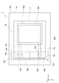
- FIG. 2 is a sectional view taken along line II-II of FIG. It is a top view of the crystal oscillator which concerns on 1st Embodiment. It is a front view of the crystal oscillator which concerns on 1st Embodiment. It is a side view of the crystal oscillator which concerns on 1st Embodiment. It is a top view of the crystal oscillator which concerns on 2nd Embodiment. It is a front view of the crystal oscillator which concerns on 2nd Embodiment. It is a front view of the crystal oscillator which concerns on 3rd Embodiment.
- FIG. 1 is an exploded perspective view of the crystal oscillator
- FIG. 2 is a sectional view taken along line II-II in a state where each configuration of the exploded perspective view of FIG. 1 is assembled.
- the illustration of various electrodes of the crystal vibrating element is omitted.
- the crystal oscillator 1 includes a crystal vibrating element 10, a cap 20, and a substrate 30.
- the crystal vibrating element 10 includes a crystal piece 11 and a first excitation electrode 14a and a second excitation electrode 14b provided on the front and back surfaces of the crystal piece 11, respectively.
- the first excitation electrode 14a is provided on the first main surface 12a of the crystal piece 11, and the second excitation electrode 14b is provided on the second main surface 12b facing the first main surface 12a of the crystal piece 11.
- the crystal piece 11 has a trigonal crystal structure different from that of a cubic system such as piezoelectric ceramic, and is formed of a crystal material having a predetermined crystal orientation.
- the crystal vibrating element 10 has, for example, an AT-cut crystal piece 11.
- the AT-cut crystal piece 11 has the Y-axis and Z-axis around the X-axis at 35 degrees 15 minutes ⁇ from the Y-axis to the Z-axis.
- the crystal piece 11 which is an AT-cut crystal piece has a longitudinal direction parallel to the X-axis direction as a first direction and a short length parallel to the Z'axis direction as a second direction orthogonal to the first direction. It has a hand direction, and further has a thickness direction parallel to the Y'axis direction as a third direction orthogonal to the first direction and the second direction.
- the crystal piece 11 is formed in a rectangular shape when the XZ'plane is viewed in a plane.
- a quartz vibration element using an AT-cut quartz piece has extremely high frequency stability over a wide temperature range and can be manufactured with excellent aging characteristics.
- the AT-cut crystal vibrating element includes a thick slide vibration mode (Thickness Shear Mode) as the main vibration.
- the crystal piece 11 has a so-called mesa structure in which the thickness of the vibrating portion is thicker than the thickness of other portions.
- the first main surface 12a of the quartz piece 11 has a convex portion 60a extending from the distal end portion to the central portion in the longitudinal direction of the quartz piece 11.
- the second main surface 12b of the crystal piece 11 has a convex portion 60b extending from the distal end portion to the central portion of the crystal piece 11 in the longitudinal direction.
- the first excitation electrode 14a is formed on the first main surface 12a of the crystal piece 11, and the second excitation electrode 14b is formed on the second main surface 12b of the crystal piece 11.
- the first excitation electrode 14a and the second excitation electrode 14b are arranged so that substantially the entire surface of the XZ'plane is overlapped with each other as a pair of electrodes when the XZ'plane is viewed in a plan view.
- the excitation electrodes 14a and 14b have a rectangular shape when the XZ'plane is viewed in a plane. For example, as shown in FIG.
- each excitation electrode 14a, 14b coincides with the lateral direction of the crystal piece 11, and the lateral direction of each excitation electrode 14a, 14b coincides with the longitudinal direction of the crystal piece 11. ing. In another embodiment, although not shown, the longitudinal direction of each excitation electrode 14a, 14b coincides with the longitudinal direction of the crystal piece 11, and the lateral direction of each excitation electrode 14a, 14b coincides with the lateral direction of the crystal piece 11. You may do it.
- the crystal piece 11 has a connection pad 16a electrically connected to the first excitation electrode 14a via an extraction electrode 15a and a connection pad 16a electrically connected to the second excitation electrode 14b via an extraction electrode 15b.
- a pad 16b is formed.
- the extraction electrode 15a is extracted from the first excitation electrode 14a on the first main surface 12a toward the short side on the negative direction side of the X axis.
- the connection pad 16a is connected to the end of the extraction electrode 15a on the negative direction side of the X axis, and extends linearly toward the short side on the positive direction side of the Z'axis.
- connection pad 16a further passes through the side surface of the crystal piece 11 on the positive direction side of the Z'axis, and extends linearly with the second main surface 12b toward the negative direction side of the Z'axis.
- the end of the connection pad 16a on the second main surface 12b on the negative direction side of the Z'axis is arranged substantially in the center of the crystal piece 11 in the Z'axis direction.
- the extraction electrode 15b is extracted from the second excitation electrode 14b on the second main surface 12b toward the short side on the negative direction side of the X axis.
- connection pad 16b is connected to the end of the extraction electrode 15b on the negative direction side of the X axis, and extends linearly toward both the positive direction side of the Z'axis and the negative direction side of the Z'axis.
- the end portion of the connection pad 16b on the positive direction side of the Z'axis is arranged substantially at the center of the crystal piece 11 in the Z'axis direction.
- the connection pads 16a and 16b are arranged along the short side on the negative side of the X-axis, and these connection pads 16a and 16b are electrically connected to the substrate 30 via the conductive adhesives 36a and 36b. It is held mechanically with.
- the conductive adhesives 36a and 36b are examples of conductive holding members.
- the arrangement and pattern shape of the connection pads 16a and 16b and the extraction electrodes 15a and 15b are not limited, and can be appropriately changed in consideration of electrical connection with other members.
- the substrate 30 includes connection pads 33a and 33b formed on the first main surface 32a, extraction electrodes 34a and 34b drawn from the connection pads 33a and 33b toward the outer edge of the first main surface 32a, and a plurality of external surfaces. Includes electrodes 35a, 35b, 35c, 35d.
- connection pad 33a is connected to the connection pad 16a of the crystal vibrating element 10 via the conductive adhesive 36a
- connection pad 33b is connected to the connection pad 16b of the crystal vibrating element 10 via the conductive adhesive 36b. It is connected to the.
- the extraction electrode 34a is drawn from the connection pad 33a toward any one corner of the substrate 30, and the extraction electrode 34b is drawn from the connection pad 33b toward the other corner of the substrate 30. There is. Further, a plurality of external electrodes 35a, 35b, 35c, 35d are formed at each corner of the substrate 30. In the example shown in FIG. 1, the extraction electrode 34a is connected to the external electrode 35a, and the extraction electrode 34b is connected to the external electrode 35b.
- the crystal oscillator 1 applies a voltage to each of the first excitation electrode 14a and the second excitation electrode 14b via the external electrodes 35a and 35b of the substrate 30. As a result, the crystal piece 11 vibrates in the vibration mode including the thickness slip vibration mode.
- the cap 20 has a recess 24 that opens facing the first main surface 32a of the substrate 30.
- the recess 24 is provided with a side wall portion 22 formed so as to rise from the bottom surface of the recess 24 over the entire circumference of the opening.
- the cap 20 has a facing surface 26 facing the first main surface 32a of the substrate 30 at the opening edge of the recess 24.
- the cap 20 may have a flange portion 28 that further protrudes from the side wall portion 22 in the outward direction of the opening. By joining the flange portion 28 and the substrate 30, the contact area between the two is increased, so that the joining strength between the two can be improved.
- the substrate 30 supports the crystal vibrating element 10 in an excitable manner.
- the substrate 30 supports the crystal vibrating element 10 in an excitable manner, for example, via the conductive adhesives 36a and 36b.
- the substrate 30 has a longitudinal direction parallel to the X-axis direction, a lateral direction parallel to the Z'axis direction, and a thickness direction parallel to the Y'axis direction, and has a rectangular shape on the XZ'plane. ing.
- the substrate 30 may be formed of, for example, an insulating ceramic, or may be formed, for example, by laminating and firing a plurality of insulating ceramic sheets.
- the substrate 30 is a glass material (for example, silicate glass or a material containing a main component other than silicate and having a glass transition phenomenon due to temperature rise), a crystal material (for example, AT-cut crystal) or a glass epoxy. It may be formed of resin or the like.
- the substrate 30 is preferably made of a heat resistant material.
- the joining material 70 joins the cap 20 and the substrate 30.
- the crystal vibrating element 10 is housed in an internal space (cavity) 23 surrounded by a recess 24 of the cap 20 and a substrate 30.
- one end on which the conductive adhesives 36a and 36b are arranged is a fixed end, and the other end is a free end.
- the joining material 70 is provided over the entire circumference of the cap 20 or the substrate 30, and is interposed between the facing surface 26 of the side wall portion 22 of the cap 20 and the first main surface 32a of the substrate 30.
- the bonding material 70 may be, for example, a glass adhesive material such as low melting point glass (for example, lead boric acid type, tin phosphoric acid type, etc.) or a resin adhesive.
- connection pad 16a has a first protrusion 40a.
- the first protrusion 40a is configured by covering the protrusion 12A formed on the second main surface 12b of the crystal piece 11 with a connection pad 16a.
- the first protrusion 40a is provided on, for example, an extension of the extraction electrode 15a drawn from the first excitation electrode 14a.
- the connection pad 16b has a first protrusion 40b. Similar to the first protrusion 40a, the first protrusion 40b is configured by covering the protrusion 12B formed on the second main surface 12b of the crystal piece 11 with the connection pad 16b. The first protrusion 40b is provided on, for example, an extension of the extraction electrode 15b drawn from the second excitation electrode 14b.
- the substrate 30 has a second protrusion 50a and a second protrusion 50b.
- the second protrusion 50a is provided corresponding to the first protrusion 40a and is electrically connected to the external electrode 35a.
- the second protrusion 50a is provided, for example, at a position facing the first protrusion 40a in the Y'axis direction in which the crystal piece 11 and the substrate 30 face each other.
- the center position of the first protrusion 40a and the center position of the second protrusion 50a coincide with each other.
- the second protrusion 50b is provided corresponding to the first protrusion 40b and is electrically connected to the external electrode 35d.
- the second protrusion 50b is provided, for example, at a position facing the first protrusion 40b in the Y'axis direction in which the crystal piece 11 and the substrate 30 face each other.
- the center position of the first protrusion 40b and the center position of the second protrusion 50a coincide with each other.
- a conductive adhesive 36a is provided between the first protrusion 40a of the connection pad 16a and the second protrusion 50a of the substrate 30.
- the conductive adhesive 36a joins between the first protrusion 40a and the second protrusion 50a.
- the conductive adhesive 36a is held around the first protrusion 40a on the second main surface 12b of the crystal piece 11 due to the surface tension. Further, the conductive adhesive 36a is held around the second protrusion 50a on the substrate 30 due to the surface tension.
- the dimension of the first protrusion 40a in the direction intersecting the protrusion direction is larger than the dimension of the second protrusion 50a in the same direction.
- the cross-sectional area of the first protrusion 40a is larger than the cross-sectional area of the second protrusion 50a in the plane cut in the direction intersecting the protrusion direction of the first protrusion 40a and the second protrusion 50a. Therefore, the wet spread of the conductive adhesive 36a on the substrate 30 having a relatively large influence on the vibration characteristics of the crystal oscillator 1 can be suppressed.
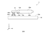
- FIG. 5 is a side view of the crystal oscillator 1. In FIG. 5, various electrodes of the crystal vibrating element are not shown.
- the protruding amount of the convex portion 60b of the crystal piece 11 is equal to the protruding amount of the protrusions 12A and 12B of the crystal piece 11.
- the regions other than the convex portion 60b and the protrusions 12A and 12B are removed by an edging process to remove the convex portion 60b and the convex portion 60b of the crystal piece 11.
- the protrusions 12A and 12B are formed.
- the amount of protrusion of the convex portion 60b of the crystal piece 11 and the amount of protrusion of the protrusions 12A and 12B may be different from each other.
- the crystal oscillator 1 is a pair of excitation electrodes 14a formed on a crystal piece 11 and a second main surface 12a opposite to the first main surface 12a and the first main surface 12a of the crystal piece 11. , 14b, a pair of connection pads 16a, 16b electrically connected to each of the pair of excitation electrodes 14a, 14b, and a pair of externals electrically connected to each of the pair of connection pads 16a, 16b.
- a substrate 30 having electrodes 35a and 35b and oscillatingly supporting the crystal piece 11 is provided, and each of the pair of connecting pads 16a and 16b has first projections 40a and 40b, and the substrate 30 has a first projection 40a and 40b.
- the second projections 50a and 50b are provided corresponding to the one projections 40a and 40b and are electrically connected to each of the pair of external electrodes 35a and 35b, and the first projections 40a and 40b and the second projections 50a, It is joined to 50b via conductive adhesives 36a and 36b. Therefore, the conductive adhesives 36a and 36b stay around the first protrusions 40a and 40b and the second protrusions 50a and 50b due to the surface tension, and the conductive adhesives between the crystal piece 11 and the substrate 30. Wet spread of 36a and 36b is suppressed. As a result, it is possible to increase the bonding strength between the substrate 30 and the crystal piece 11 while suppressing the vibration characteristics of the crystal piece 11 from deviating from the desired characteristics due to the stress acting on the crystal piece 11 from the substrate 30. can.
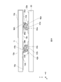
- FIG. 6 is a plan view schematically showing an example of the structure of the crystal oscillator 1 according to the present embodiment.
- the crystal oscillator 1 according to the present embodiment is between the first projections 40a and 40b of the crystal piece 11 and the second projections 50a and 50b of the substrate 30 in comparison with the crystal oscillator 1 described in the first embodiment.
- they are common in that they are joined using the conductive adhesives 36a and 36b, the first protrusions 40a and 40b of the crystal piece 11 and the second protrusions 50a and 50b of the substrate 30 are the conductive adhesives 36a and 36b. It is different from the first embodiment in that it is diagonally joined by using.
- the first projections 40a and 40b are more crystals than the connection portions with the extraction electrodes 15a and 15b in the connection pads 16a and 16b. It is provided inside the piece 11.
- the first projection 40a is located, for example, on the Z'axis negative direction side of the extension line of the extraction electrode 15a drawn from the first excitation electrode 14a.
- the first projection 40b is located, for example, on the Z'axis positive direction side of the extension line of the extraction electrode 15b drawn from the second excitation electrode 14b.
- the direction in which the pair of extraction electrodes 15a and 15b are drawn out from each of the pair of excitation electrodes 14a and 14b is defined as the first direction (X-axis direction), and the direction intersecting the first direction is defined as the second direction (Z'axis direction).
- the distance between the first projections 40a and 40b corresponding to each of the pair of connection pads 16a and 16b in the second direction is less than half of the respective dimensions of the pair of excitation electrodes 14a and 14b in the second direction. ..
- the stress acting on the crystal piece 11 from the substrate 30 can be further reduced, and the influence on the vibration characteristics of the crystal piece 11 can be reduced.
- the substrate 30 is provided corresponding to the first protrusion 40a and has a second protrusion 50a electrically connected to the external electrode 35a.
- the second projection 50a is provided at a position facing the first projection 40a, for example, in a direction in which the crystal piece 11 and the substrate 30 intersect diagonally with respect to the Y'axis direction.
- the center position of the first protrusion 40a and the center position of the second protrusion 50a of the second protrusion 50a are different from each other when the XZ'plane is viewed in a plan view.
- the second protrusion 50a is arranged on the negative direction side of the Z'axis with respect to the first protrusion 40a, for example, when the XZ'plane is viewed in a plan view.
- the substrate 30 has a second protrusion 50b that is provided corresponding to the first protrusion 40b and is electrically connected to the external electrode 35b.
- the second projection 50b is provided at a position facing the first projection 40b, for example, in a direction in which the crystal piece 11 and the substrate 30 intersect diagonally with respect to the Y'axis direction.
- the center position of the first protrusion 40b and the center position of the second protrusion 50b of the second protrusion 50b are different from each other when the XZ'plane is viewed in a plan view.
- the second protrusion 50b is arranged on the Z'axis positive direction side with respect to the first protrusion 40b, for example, when the XZ'plane is viewed in a plan view.
- each of the pair of first protrusions 40a and 40b is provided corresponding to each of the pair of first protrusions 40a and 40b as compared with the distance between the pair of first protrusions 40a and 40b provided on each of the pair of connection pads 16a and 16b.
- the distance between the pair of second protrusions 50a and 50b is narrow. That is, in a plan view of the first protrusion 40a and the second protrusion 50a from the protrusion direction, the dimension of the second protrusion 50a in the direction intersecting the protrusion direction is smaller than the dimension of the first protrusion 40a in the same direction.
- the pair of second protrusions 50a and 50b can be arranged even closer to each other while preventing a short circuit between the pair of second protrusions 50a and 50b.
- the stress acting on the crystal piece 11 from the substrate 30 can be further reduced, and the influence on the vibration characteristics of the crystal piece 11 can be reduced.
- each of the pair of connection pads 16a and 16b is connected to the pair of extraction electrodes 15a and 15b drawn from each of the pair of excitation electrodes 14a and 14b, and the first projection is formed.
- the 40a is arranged inside the crystal piece 11 with respect to the connection portion between each of the pair of connection pads 16a and 16b and each of the pair of extraction electrodes 15a and 15b.
- FIG. 8 is a plan view schematically showing an example of the structure of the crystal oscillator 1 according to the present embodiment.
- the crystal oscillator 1 according to the present embodiment is between the first projections 40a and 40b of the crystal piece 11 and the second projections 50a and 50b of the substrate 30 in comparison with the crystal oscillator 1 described in the second embodiment.
- they are common in that they are joined using the conductive adhesives 36a and 36b, grooves are formed at the tips of the first protrusions 40a and 40b of the crystal piece 11 and the second protrusions 50a and 50b of the substrate 30. The point is different from the second embodiment.
- groove portions 42a and 42b are formed at the tips of the first projections 40a and 40b of the quartz piece 11.
- the grooves 42a and 42b are, for example, slits.
- groove portions 52a and 52b are formed at the tips of the second protrusions 50a and 50b of the substrate 30.
- the grooves 52a and 52b are, for example, slits.
- Conductive adhesives 36a and 36b are provided between the first protrusions 40a and 40b of the crystal piece 11 and the second protrusions 50a and 50b of the substrate 30.
- the conductive adhesives 36a and 36b are filled inside the grooves 42a and 42b of the first protrusions 40a and 40b of the crystal piece 11 and the grooves 52a and 52b of the second protrusions 50a and 50b of the substrate 30.
- the crystal oscillator 1 In the crystal oscillator 1 according to the present embodiment, at least one of the tips of the first protrusions 40a and 40b and the second protrusions 50a and 50b has groove portions 42a, 42b, 52a and 52b. Therefore, the contact area between the conductive adhesives 36a and 36b and the first protrusions 40a and 40b of the crystal piece 11 and the second protrusions 50a and 50b of the substrate 30 increases. As a result, the bonding strength between the first protrusions 40a and 40b of the crystal piece 11 and the second protrusions 50a and 50b of the substrate 30 is increased without increasing the thickness of the first protrusions 40a and 40b and the second protrusions 50a and 50b. Can be secured. Therefore, by narrowing the distance between the pair of first protrusions 40a and 40b and the distance between the pair of second protrusions 50a and 50b, the stress acting on the crystal piece 11 from the substrate 30 can be further reduced.
- connection pads 16a and 16b are coated with a conductive film and then other than the first protrusions 40a and 40b.
- the first projections 40a and 40b of the connecting pads 16a and 16b may be formed by removing the region of the above by an edging process.
- a groove may be formed at the tips of the first protrusions 40a and 40b of the crystal piece 11 and the tips of the second protrusions 50a and 50b of the substrate 30.
- Each of the connecting pads of the above has a first projection, and the substrate has a second projection corresponding to the first projection and electrically connected to each of the pair of external electrodes.
- a crystal oscillator is provided, which is joined between the protrusion and the second protrusion via a conductive holding member.
- each of the pair of connecting pads is connected to a pair of drawer electrodes drawn from each of the pair of excitation electrodes, and the first projection is each of the pair of connecting pads and each of the pair of drawer electrodes.
- a crystal oscillator which is located inside the crystal piece from the connection site with the crystal piece, is provided.
- the direction in which the pair of extraction electrodes is drawn out from each of the pair of excitation electrodes is the first direction and the direction intersecting the first direction is the second direction, it corresponds to each of the pair of connection pads.
- a crystal oscillator is provided in which the distance between the first projections in the second direction is less than half the size of each of the pair of excitation electrodes in the second direction.
- a crystal oscillator in which the center position of the first protrusion and the center position of the second protrusion are different from each other in a plan view seen from the protrusion direction of the first protrusion and the second protrusion.
- the dimension of the first protrusion in the direction intersecting the protruding direction is larger than the dimension of the second protrusion in the same direction.
- a quartz oscillator in which the tip of at least one of the first protrusion and the second protrusion has a groove.
- the distance between the pair of second protrusions provided corresponding to each of the pair of first protrusions is narrower than the distance between the pair of first protrusions provided on each of the pair of connection pads.
- a crystal oscillator is provided.
- Crystal oscillator 10 Crystal vibration element 11 Crystal piece 12A Protrusion 12a 1st main surface 12B Protrusion 12b 2nd main surface 14a 1st excitation electrode 14b 2nd excitation electrode 15a Extract electrode 15b Extract electrode 16a Connection pad 16b Connection pad 36a Conductive adhesive 36b Conductive adhesive 40a First protrusion 40b First protrusion 50a Second protrusion 50b Second protrusion 52a Groove 52b Groove
Landscapes
- Physics & Mathematics (AREA)
- Acoustics & Sound (AREA)
- Piezo-Electric Or Mechanical Vibrators, Or Delay Or Filter Circuits (AREA)
Priority Applications (1)
| Application Number | Priority Date | Filing Date | Title |
|---|---|---|---|
| JP2022532258A JP7392855B2 (ja) | 2020-06-26 | 2021-01-07 | 水晶振動子 |
Applications Claiming Priority (2)
| Application Number | Priority Date | Filing Date | Title |
|---|---|---|---|
| JP2020110375 | 2020-06-26 | ||
| JP2020-110375 | 2020-06-26 |
Publications (1)
| Publication Number | Publication Date |
|---|---|
| WO2021260978A1 true WO2021260978A1 (ja) | 2021-12-30 |
Family
ID=79282253
Family Applications (1)
| Application Number | Title | Priority Date | Filing Date |
|---|---|---|---|
| PCT/JP2021/000280 Ceased WO2021260978A1 (ja) | 2020-06-26 | 2021-01-07 | 水晶振動子 |
Country Status (2)
| Country | Link |
|---|---|
| JP (1) | JP7392855B2 (https=) |
| WO (1) | WO2021260978A1 (https=) |
Citations (6)
| Publication number | Priority date | Publication date | Assignee | Title |
|---|---|---|---|---|
| JPH1022776A (ja) * | 1996-07-03 | 1998-01-23 | Seiko Epson Corp | 圧電振動子 |
| JP2007096528A (ja) * | 2005-09-27 | 2007-04-12 | Epson Toyocom Corp | 圧電振動素子の支持構造、表面実装用圧電振動子、表面実装用圧電発振器、及び圧電振動素子の搭載方法 |
| JP2008252795A (ja) * | 2007-03-30 | 2008-10-16 | Daishinku Corp | 圧電振動デバイス |
| JP2011205426A (ja) * | 2010-03-25 | 2011-10-13 | Seiko Epson Corp | 電子部品の実装構造体および電子部品の製造方法 |
| JP2011205429A (ja) * | 2010-03-25 | 2011-10-13 | Seiko Epson Corp | 電子部品 |
| US20170005636A1 (en) * | 2015-07-01 | 2017-01-05 | Samsung Electro-Mechanics Co., Ltd. | Crystal oscillator package |
Family Cites Families (1)
| Publication number | Priority date | Publication date | Assignee | Title |
|---|---|---|---|---|
| JP2009081670A (ja) * | 2007-09-26 | 2009-04-16 | Daishinku Corp | 圧電振動デバイス、およびその製造方法 |
-
2021
- 2021-01-07 WO PCT/JP2021/000280 patent/WO2021260978A1/ja not_active Ceased
- 2021-01-07 JP JP2022532258A patent/JP7392855B2/ja active Active
Patent Citations (6)
| Publication number | Priority date | Publication date | Assignee | Title |
|---|---|---|---|---|
| JPH1022776A (ja) * | 1996-07-03 | 1998-01-23 | Seiko Epson Corp | 圧電振動子 |
| JP2007096528A (ja) * | 2005-09-27 | 2007-04-12 | Epson Toyocom Corp | 圧電振動素子の支持構造、表面実装用圧電振動子、表面実装用圧電発振器、及び圧電振動素子の搭載方法 |
| JP2008252795A (ja) * | 2007-03-30 | 2008-10-16 | Daishinku Corp | 圧電振動デバイス |
| JP2011205426A (ja) * | 2010-03-25 | 2011-10-13 | Seiko Epson Corp | 電子部品の実装構造体および電子部品の製造方法 |
| JP2011205429A (ja) * | 2010-03-25 | 2011-10-13 | Seiko Epson Corp | 電子部品 |
| US20170005636A1 (en) * | 2015-07-01 | 2017-01-05 | Samsung Electro-Mechanics Co., Ltd. | Crystal oscillator package |
Also Published As
| Publication number | Publication date |
|---|---|
| JPWO2021260978A1 (https=) | 2021-12-30 |
| JP7392855B2 (ja) | 2023-12-06 |
Similar Documents
| Publication | Publication Date | Title |
|---|---|---|
| US6111480A (en) | Piezoelectric resonator and method of adjusting resonant frequency thereof | |
| CN109314502B (zh) | 水晶振动元件、水晶振子以及水晶振动元件的制造方法 | |
| CN101557207A (zh) | 压电振动装置 | |
| KR100330128B1 (ko) | 압전 공진자 | |
| JP2012039226A (ja) | 音叉型の圧電振動片および圧電デバイス | |
| CN102957395A (zh) | 台面型石英晶体振动件及石英晶体装置 | |
| US7902731B2 (en) | Piezoelectric resonator device and method for manufacturing the same | |
| JP2012249099A (ja) | 圧電振動片 | |
| JP2012156592A (ja) | 圧電振動片、圧電振動子、電子デバイス | |
| JP2012186639A (ja) | 圧電振動片、圧電振動子、電子デバイス | |
| US10938368B2 (en) | Piezoelectric-resonator-mounting substrate, and piezoelectric resonator unit and method of manufacturing the piezoelectric resonator unit | |
| WO2021260978A1 (ja) | 水晶振動子 | |
| JP2015173366A (ja) | 圧電振動片及び圧電デバイス | |
| CN109690940B (zh) | 水晶振子及其制造方法 | |
| WO2017068809A1 (ja) | 圧電振動子 | |
| CN1761152B (zh) | 表面贴装石英晶体振荡器 | |
| CN107210725A (zh) | 水晶振子以及水晶振动器件 | |
| JP7302618B2 (ja) | 水晶振動子およびその製造方法 | |
| JP7227571B2 (ja) | 振動素子、振動子及び振動素子の製造方法 | |
| JP5949445B2 (ja) | 圧電フィルタ | |
| JP6555500B2 (ja) | 圧電振動素子及び圧電振動子 | |
| JP7061275B2 (ja) | 水晶振動素子および水晶振動子 | |
| JPH0344979A (ja) | チップ状圧電部品 | |
| US20260031785A1 (en) | Crystal resonator plate and crystal resonator device | |
| JPH0575376A (ja) | 圧電音叉型共振子 |
Legal Events
| Date | Code | Title | Description |
|---|---|---|---|
| 121 | Ep: the epo has been informed by wipo that ep was designated in this application |
Ref document number: 21828625 Country of ref document: EP Kind code of ref document: A1 |
|
| ENP | Entry into the national phase |
Ref document number: 2022532258 Country of ref document: JP Kind code of ref document: A |
|
| NENP | Non-entry into the national phase |
Ref country code: DE |
|
| 122 | Ep: pct application non-entry in european phase |
Ref document number: 21828625 Country of ref document: EP Kind code of ref document: A1 |