WO2021260978A1 - Crystal oscillator - Google Patents
Crystal oscillator Download PDFInfo
- Publication number
- WO2021260978A1 WO2021260978A1 PCT/JP2021/000280 JP2021000280W WO2021260978A1 WO 2021260978 A1 WO2021260978 A1 WO 2021260978A1 JP 2021000280 W JP2021000280 W JP 2021000280W WO 2021260978 A1 WO2021260978 A1 WO 2021260978A1
- Authority
- WO
- WIPO (PCT)
- Prior art keywords
- pair
- protrusion
- crystal
- substrate
- electrodes
- Prior art date
Links
- 239000013078 crystal Substances 0.000 title claims abstract description 147
- 230000005284 excitation Effects 0.000 claims abstract description 44
- 239000000758 substrate Substances 0.000 claims description 58
- 238000000605 extraction Methods 0.000 claims description 23
- 239000010453 quartz Substances 0.000 claims description 16
- VYPSYNLAJGMNEJ-UHFFFAOYSA-N silicon dioxide Inorganic materials O=[Si]=O VYPSYNLAJGMNEJ-UHFFFAOYSA-N 0.000 claims description 16
- 239000000853 adhesive Substances 0.000 description 27
- 230000001070 adhesive effect Effects 0.000 description 27
- 239000000463 material Substances 0.000 description 9
- 230000035882 stress Effects 0.000 description 6
- 239000011521 glass Substances 0.000 description 4
- 239000000919 ceramic Substances 0.000 description 3
- 238000007688 edging Methods 0.000 description 2
- 230000000694 effects Effects 0.000 description 2
- 238000000034 method Methods 0.000 description 2
- 239000011347 resin Substances 0.000 description 2
- 229920005989 resin Polymers 0.000 description 2
- 239000004593 Epoxy Substances 0.000 description 1
- BPQQTUXANYXVAA-UHFFFAOYSA-N Orthosilicate Chemical compound [O-][Si]([O-])([O-])[O-] BPQQTUXANYXVAA-UHFFFAOYSA-N 0.000 description 1
- QYIJPFYCTROKTM-UHFFFAOYSA-N [Sn].P(O)(O)(O)=O Chemical compound [Sn].P(O)(O)(O)=O QYIJPFYCTROKTM-UHFFFAOYSA-N 0.000 description 1
- 230000032683 aging Effects 0.000 description 1
- KGBXLFKZBHKPEV-UHFFFAOYSA-N boric acid Chemical compound OB(O)O KGBXLFKZBHKPEV-UHFFFAOYSA-N 0.000 description 1
- 239000004327 boric acid Substances 0.000 description 1
- 238000005516 engineering process Methods 0.000 description 1
- 238000010304 firing Methods 0.000 description 1
- 230000009477 glass transition Effects 0.000 description 1
- 239000003779 heat-resistant material Substances 0.000 description 1
- 238000010030 laminating Methods 0.000 description 1
- 238000004519 manufacturing process Methods 0.000 description 1
- 238000002844 melting Methods 0.000 description 1
- 230000008018 melting Effects 0.000 description 1
- 239000005368 silicate glass Substances 0.000 description 1
Images


Classifications
-
- H—ELECTRICITY
- H03—ELECTRONIC CIRCUITRY
- H03H—IMPEDANCE NETWORKS, e.g. RESONANT CIRCUITS; RESONATORS
- H03H9/00—Networks comprising electromechanical or electro-acoustic devices; Electromechanical resonators
- H03H9/02—Details
- H03H9/05—Holders; Supports
- H03H9/10—Mounting in enclosures
-
- H—ELECTRICITY
- H03—ELECTRONIC CIRCUITRY
- H03H—IMPEDANCE NETWORKS, e.g. RESONANT CIRCUITS; RESONATORS
- H03H9/00—Networks comprising electromechanical or electro-acoustic devices; Electromechanical resonators
- H03H9/15—Constructional features of resonators consisting of piezoelectric or electrostrictive material
- H03H9/17—Constructional features of resonators consisting of piezoelectric or electrostrictive material having a single resonator
- H03H9/19—Constructional features of resonators consisting of piezoelectric or electrostrictive material having a single resonator consisting of quartz
Definitions
- the present invention relates to a quartz oscillator.
- a crystal oscillator whose main vibration is thick slip vibration is widely used as a signal source for a reference signal used in an oscillator or a band filter.
- a convex portion provided on a quartz piece is pressed against a bonding pad coated with a conductive adhesive, and then the conductive adhesive is heated and cured to form a base package.
- the configuration for joining the crystal pieces is disclosed.
- the conductive adhesive is adhered so that the hem is wet and spread. Therefore, due to the stress acting on the crystal piece from the package, the vibration characteristic of the crystal piece may deviate from the desired characteristic.
- the present invention has been made in view of such circumstances, and provides a crystal oscillator capable of increasing the bonding strength between a substrate and a quartz piece while making the vibration characteristic of the quartz piece a desired characteristic.
- the purpose is to increase the bonding strength between a substrate and a quartz piece while making the vibration characteristic of the quartz piece a desired characteristic.
- the crystal oscillator includes a crystal piece, a pair of excitation electrodes formed on a first main surface of the crystal piece and a second main surface opposite to the first main surface, and the above-mentioned It has a pair of connection pads electrically connected to each of the pair of excitation electrodes and a pair of external electrodes electrically connected to each of the pair of connection pads, and can excite the crystal piece.
- Each of the pair of connecting pads comprises a supporting substrate, each of which has a first projection, the substrate being provided corresponding to the first projection and electrically with each of the pair of external electrodes. It has a connected second protrusion, and the first protrusion and the second protrusion are joined via a conductive holding member.
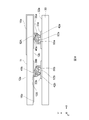
- FIG. 2 is a sectional view taken along line II-II of FIG. It is a top view of the crystal oscillator which concerns on 1st Embodiment. It is a front view of the crystal oscillator which concerns on 1st Embodiment. It is a side view of the crystal oscillator which concerns on 1st Embodiment. It is a top view of the crystal oscillator which concerns on 2nd Embodiment. It is a front view of the crystal oscillator which concerns on 2nd Embodiment. It is a front view of the crystal oscillator which concerns on 3rd Embodiment.
- FIG. 1 is an exploded perspective view of the crystal oscillator
- FIG. 2 is a sectional view taken along line II-II in a state where each configuration of the exploded perspective view of FIG. 1 is assembled.
- the illustration of various electrodes of the crystal vibrating element is omitted.
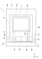
- the crystal oscillator 1 includes a crystal vibrating element 10, a cap 20, and a substrate 30.
- the crystal vibrating element 10 includes a crystal piece 11 and a first excitation electrode 14a and a second excitation electrode 14b provided on the front and back surfaces of the crystal piece 11, respectively.
- the first excitation electrode 14a is provided on the first main surface 12a of the crystal piece 11, and the second excitation electrode 14b is provided on the second main surface 12b facing the first main surface 12a of the crystal piece 11.
- the crystal piece 11 has a trigonal crystal structure different from that of a cubic system such as piezoelectric ceramic, and is formed of a crystal material having a predetermined crystal orientation.
- the crystal vibrating element 10 has, for example, an AT-cut crystal piece 11.
- the AT-cut crystal piece 11 has the Y-axis and Z-axis around the X-axis at 35 degrees 15 minutes ⁇ from the Y-axis to the Z-axis.
- the crystal piece 11 which is an AT-cut crystal piece has a longitudinal direction parallel to the X-axis direction as a first direction and a short length parallel to the Z'axis direction as a second direction orthogonal to the first direction. It has a hand direction, and further has a thickness direction parallel to the Y'axis direction as a third direction orthogonal to the first direction and the second direction.
- the crystal piece 11 is formed in a rectangular shape when the XZ'plane is viewed in a plane.
- a quartz vibration element using an AT-cut quartz piece has extremely high frequency stability over a wide temperature range and can be manufactured with excellent aging characteristics.
- the AT-cut crystal vibrating element includes a thick slide vibration mode (Thickness Shear Mode) as the main vibration.
- the crystal piece 11 has a so-called mesa structure in which the thickness of the vibrating portion is thicker than the thickness of other portions.
- the first main surface 12a of the quartz piece 11 has a convex portion 60a extending from the distal end portion to the central portion in the longitudinal direction of the quartz piece 11.
- the second main surface 12b of the crystal piece 11 has a convex portion 60b extending from the distal end portion to the central portion of the crystal piece 11 in the longitudinal direction.
- the first excitation electrode 14a is formed on the first main surface 12a of the crystal piece 11, and the second excitation electrode 14b is formed on the second main surface 12b of the crystal piece 11.
- the first excitation electrode 14a and the second excitation electrode 14b are arranged so that substantially the entire surface of the XZ'plane is overlapped with each other as a pair of electrodes when the XZ'plane is viewed in a plan view.
- the excitation electrodes 14a and 14b have a rectangular shape when the XZ'plane is viewed in a plane. For example, as shown in FIG.
- each excitation electrode 14a, 14b coincides with the lateral direction of the crystal piece 11, and the lateral direction of each excitation electrode 14a, 14b coincides with the longitudinal direction of the crystal piece 11. ing. In another embodiment, although not shown, the longitudinal direction of each excitation electrode 14a, 14b coincides with the longitudinal direction of the crystal piece 11, and the lateral direction of each excitation electrode 14a, 14b coincides with the lateral direction of the crystal piece 11. You may do it.
- the crystal piece 11 has a connection pad 16a electrically connected to the first excitation electrode 14a via an extraction electrode 15a and a connection pad 16a electrically connected to the second excitation electrode 14b via an extraction electrode 15b.
- a pad 16b is formed.
- the extraction electrode 15a is extracted from the first excitation electrode 14a on the first main surface 12a toward the short side on the negative direction side of the X axis.
- the connection pad 16a is connected to the end of the extraction electrode 15a on the negative direction side of the X axis, and extends linearly toward the short side on the positive direction side of the Z'axis.
- connection pad 16a further passes through the side surface of the crystal piece 11 on the positive direction side of the Z'axis, and extends linearly with the second main surface 12b toward the negative direction side of the Z'axis.
- the end of the connection pad 16a on the second main surface 12b on the negative direction side of the Z'axis is arranged substantially in the center of the crystal piece 11 in the Z'axis direction.
- the extraction electrode 15b is extracted from the second excitation electrode 14b on the second main surface 12b toward the short side on the negative direction side of the X axis.
- connection pad 16b is connected to the end of the extraction electrode 15b on the negative direction side of the X axis, and extends linearly toward both the positive direction side of the Z'axis and the negative direction side of the Z'axis.
- the end portion of the connection pad 16b on the positive direction side of the Z'axis is arranged substantially at the center of the crystal piece 11 in the Z'axis direction.
- the connection pads 16a and 16b are arranged along the short side on the negative side of the X-axis, and these connection pads 16a and 16b are electrically connected to the substrate 30 via the conductive adhesives 36a and 36b. It is held mechanically with.
- the conductive adhesives 36a and 36b are examples of conductive holding members.
- the arrangement and pattern shape of the connection pads 16a and 16b and the extraction electrodes 15a and 15b are not limited, and can be appropriately changed in consideration of electrical connection with other members.
- the substrate 30 includes connection pads 33a and 33b formed on the first main surface 32a, extraction electrodes 34a and 34b drawn from the connection pads 33a and 33b toward the outer edge of the first main surface 32a, and a plurality of external surfaces. Includes electrodes 35a, 35b, 35c, 35d.
- connection pad 33a is connected to the connection pad 16a of the crystal vibrating element 10 via the conductive adhesive 36a
- connection pad 33b is connected to the connection pad 16b of the crystal vibrating element 10 via the conductive adhesive 36b. It is connected to the.
- the extraction electrode 34a is drawn from the connection pad 33a toward any one corner of the substrate 30, and the extraction electrode 34b is drawn from the connection pad 33b toward the other corner of the substrate 30. There is. Further, a plurality of external electrodes 35a, 35b, 35c, 35d are formed at each corner of the substrate 30. In the example shown in FIG. 1, the extraction electrode 34a is connected to the external electrode 35a, and the extraction electrode 34b is connected to the external electrode 35b.
- the crystal oscillator 1 applies a voltage to each of the first excitation electrode 14a and the second excitation electrode 14b via the external electrodes 35a and 35b of the substrate 30. As a result, the crystal piece 11 vibrates in the vibration mode including the thickness slip vibration mode.
- the cap 20 has a recess 24 that opens facing the first main surface 32a of the substrate 30.
- the recess 24 is provided with a side wall portion 22 formed so as to rise from the bottom surface of the recess 24 over the entire circumference of the opening.
- the cap 20 has a facing surface 26 facing the first main surface 32a of the substrate 30 at the opening edge of the recess 24.
- the cap 20 may have a flange portion 28 that further protrudes from the side wall portion 22 in the outward direction of the opening. By joining the flange portion 28 and the substrate 30, the contact area between the two is increased, so that the joining strength between the two can be improved.
- the substrate 30 supports the crystal vibrating element 10 in an excitable manner.
- the substrate 30 supports the crystal vibrating element 10 in an excitable manner, for example, via the conductive adhesives 36a and 36b.
- the substrate 30 has a longitudinal direction parallel to the X-axis direction, a lateral direction parallel to the Z'axis direction, and a thickness direction parallel to the Y'axis direction, and has a rectangular shape on the XZ'plane. ing.
- the substrate 30 may be formed of, for example, an insulating ceramic, or may be formed, for example, by laminating and firing a plurality of insulating ceramic sheets.
- the substrate 30 is a glass material (for example, silicate glass or a material containing a main component other than silicate and having a glass transition phenomenon due to temperature rise), a crystal material (for example, AT-cut crystal) or a glass epoxy. It may be formed of resin or the like.
- the substrate 30 is preferably made of a heat resistant material.
- the joining material 70 joins the cap 20 and the substrate 30.
- the crystal vibrating element 10 is housed in an internal space (cavity) 23 surrounded by a recess 24 of the cap 20 and a substrate 30.
- one end on which the conductive adhesives 36a and 36b are arranged is a fixed end, and the other end is a free end.
- the joining material 70 is provided over the entire circumference of the cap 20 or the substrate 30, and is interposed between the facing surface 26 of the side wall portion 22 of the cap 20 and the first main surface 32a of the substrate 30.
- the bonding material 70 may be, for example, a glass adhesive material such as low melting point glass (for example, lead boric acid type, tin phosphoric acid type, etc.) or a resin adhesive.
- connection pad 16a has a first protrusion 40a.
- the first protrusion 40a is configured by covering the protrusion 12A formed on the second main surface 12b of the crystal piece 11 with a connection pad 16a.
- the first protrusion 40a is provided on, for example, an extension of the extraction electrode 15a drawn from the first excitation electrode 14a.
- the connection pad 16b has a first protrusion 40b. Similar to the first protrusion 40a, the first protrusion 40b is configured by covering the protrusion 12B formed on the second main surface 12b of the crystal piece 11 with the connection pad 16b. The first protrusion 40b is provided on, for example, an extension of the extraction electrode 15b drawn from the second excitation electrode 14b.
- the substrate 30 has a second protrusion 50a and a second protrusion 50b.
- the second protrusion 50a is provided corresponding to the first protrusion 40a and is electrically connected to the external electrode 35a.
- the second protrusion 50a is provided, for example, at a position facing the first protrusion 40a in the Y'axis direction in which the crystal piece 11 and the substrate 30 face each other.
- the center position of the first protrusion 40a and the center position of the second protrusion 50a coincide with each other.
- the second protrusion 50b is provided corresponding to the first protrusion 40b and is electrically connected to the external electrode 35d.
- the second protrusion 50b is provided, for example, at a position facing the first protrusion 40b in the Y'axis direction in which the crystal piece 11 and the substrate 30 face each other.
- the center position of the first protrusion 40b and the center position of the second protrusion 50a coincide with each other.
- a conductive adhesive 36a is provided between the first protrusion 40a of the connection pad 16a and the second protrusion 50a of the substrate 30.
- the conductive adhesive 36a joins between the first protrusion 40a and the second protrusion 50a.
- the conductive adhesive 36a is held around the first protrusion 40a on the second main surface 12b of the crystal piece 11 due to the surface tension. Further, the conductive adhesive 36a is held around the second protrusion 50a on the substrate 30 due to the surface tension.
- the dimension of the first protrusion 40a in the direction intersecting the protrusion direction is larger than the dimension of the second protrusion 50a in the same direction.
- the cross-sectional area of the first protrusion 40a is larger than the cross-sectional area of the second protrusion 50a in the plane cut in the direction intersecting the protrusion direction of the first protrusion 40a and the second protrusion 50a. Therefore, the wet spread of the conductive adhesive 36a on the substrate 30 having a relatively large influence on the vibration characteristics of the crystal oscillator 1 can be suppressed.
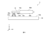
- FIG. 5 is a side view of the crystal oscillator 1. In FIG. 5, various electrodes of the crystal vibrating element are not shown.
- the protruding amount of the convex portion 60b of the crystal piece 11 is equal to the protruding amount of the protrusions 12A and 12B of the crystal piece 11.
- the regions other than the convex portion 60b and the protrusions 12A and 12B are removed by an edging process to remove the convex portion 60b and the convex portion 60b of the crystal piece 11.
- the protrusions 12A and 12B are formed.
- the amount of protrusion of the convex portion 60b of the crystal piece 11 and the amount of protrusion of the protrusions 12A and 12B may be different from each other.
- the crystal oscillator 1 is a pair of excitation electrodes 14a formed on a crystal piece 11 and a second main surface 12a opposite to the first main surface 12a and the first main surface 12a of the crystal piece 11. , 14b, a pair of connection pads 16a, 16b electrically connected to each of the pair of excitation electrodes 14a, 14b, and a pair of externals electrically connected to each of the pair of connection pads 16a, 16b.
- a substrate 30 having electrodes 35a and 35b and oscillatingly supporting the crystal piece 11 is provided, and each of the pair of connecting pads 16a and 16b has first projections 40a and 40b, and the substrate 30 has a first projection 40a and 40b.
- the second projections 50a and 50b are provided corresponding to the one projections 40a and 40b and are electrically connected to each of the pair of external electrodes 35a and 35b, and the first projections 40a and 40b and the second projections 50a, It is joined to 50b via conductive adhesives 36a and 36b. Therefore, the conductive adhesives 36a and 36b stay around the first protrusions 40a and 40b and the second protrusions 50a and 50b due to the surface tension, and the conductive adhesives between the crystal piece 11 and the substrate 30. Wet spread of 36a and 36b is suppressed. As a result, it is possible to increase the bonding strength between the substrate 30 and the crystal piece 11 while suppressing the vibration characteristics of the crystal piece 11 from deviating from the desired characteristics due to the stress acting on the crystal piece 11 from the substrate 30. can.
- FIG. 6 is a plan view schematically showing an example of the structure of the crystal oscillator 1 according to the present embodiment.
- the crystal oscillator 1 according to the present embodiment is between the first projections 40a and 40b of the crystal piece 11 and the second projections 50a and 50b of the substrate 30 in comparison with the crystal oscillator 1 described in the first embodiment.
- they are common in that they are joined using the conductive adhesives 36a and 36b, the first protrusions 40a and 40b of the crystal piece 11 and the second protrusions 50a and 50b of the substrate 30 are the conductive adhesives 36a and 36b. It is different from the first embodiment in that it is diagonally joined by using.
- the first projections 40a and 40b are more crystals than the connection portions with the extraction electrodes 15a and 15b in the connection pads 16a and 16b. It is provided inside the piece 11.
- the first projection 40a is located, for example, on the Z'axis negative direction side of the extension line of the extraction electrode 15a drawn from the first excitation electrode 14a.
- the first projection 40b is located, for example, on the Z'axis positive direction side of the extension line of the extraction electrode 15b drawn from the second excitation electrode 14b.
- the direction in which the pair of extraction electrodes 15a and 15b are drawn out from each of the pair of excitation electrodes 14a and 14b is defined as the first direction (X-axis direction), and the direction intersecting the first direction is defined as the second direction (Z'axis direction).
- the distance between the first projections 40a and 40b corresponding to each of the pair of connection pads 16a and 16b in the second direction is less than half of the respective dimensions of the pair of excitation electrodes 14a and 14b in the second direction. ..
- the stress acting on the crystal piece 11 from the substrate 30 can be further reduced, and the influence on the vibration characteristics of the crystal piece 11 can be reduced.
- the substrate 30 is provided corresponding to the first protrusion 40a and has a second protrusion 50a electrically connected to the external electrode 35a.
- the second projection 50a is provided at a position facing the first projection 40a, for example, in a direction in which the crystal piece 11 and the substrate 30 intersect diagonally with respect to the Y'axis direction.
- the center position of the first protrusion 40a and the center position of the second protrusion 50a of the second protrusion 50a are different from each other when the XZ'plane is viewed in a plan view.
- the second protrusion 50a is arranged on the negative direction side of the Z'axis with respect to the first protrusion 40a, for example, when the XZ'plane is viewed in a plan view.
- the substrate 30 has a second protrusion 50b that is provided corresponding to the first protrusion 40b and is electrically connected to the external electrode 35b.
- the second projection 50b is provided at a position facing the first projection 40b, for example, in a direction in which the crystal piece 11 and the substrate 30 intersect diagonally with respect to the Y'axis direction.
- the center position of the first protrusion 40b and the center position of the second protrusion 50b of the second protrusion 50b are different from each other when the XZ'plane is viewed in a plan view.
- the second protrusion 50b is arranged on the Z'axis positive direction side with respect to the first protrusion 40b, for example, when the XZ'plane is viewed in a plan view.
- each of the pair of first protrusions 40a and 40b is provided corresponding to each of the pair of first protrusions 40a and 40b as compared with the distance between the pair of first protrusions 40a and 40b provided on each of the pair of connection pads 16a and 16b.
- the distance between the pair of second protrusions 50a and 50b is narrow. That is, in a plan view of the first protrusion 40a and the second protrusion 50a from the protrusion direction, the dimension of the second protrusion 50a in the direction intersecting the protrusion direction is smaller than the dimension of the first protrusion 40a in the same direction.
- the pair of second protrusions 50a and 50b can be arranged even closer to each other while preventing a short circuit between the pair of second protrusions 50a and 50b.
- the stress acting on the crystal piece 11 from the substrate 30 can be further reduced, and the influence on the vibration characteristics of the crystal piece 11 can be reduced.
- each of the pair of connection pads 16a and 16b is connected to the pair of extraction electrodes 15a and 15b drawn from each of the pair of excitation electrodes 14a and 14b, and the first projection is formed.
- the 40a is arranged inside the crystal piece 11 with respect to the connection portion between each of the pair of connection pads 16a and 16b and each of the pair of extraction electrodes 15a and 15b.
- FIG. 8 is a plan view schematically showing an example of the structure of the crystal oscillator 1 according to the present embodiment.
- the crystal oscillator 1 according to the present embodiment is between the first projections 40a and 40b of the crystal piece 11 and the second projections 50a and 50b of the substrate 30 in comparison with the crystal oscillator 1 described in the second embodiment.
- they are common in that they are joined using the conductive adhesives 36a and 36b, grooves are formed at the tips of the first protrusions 40a and 40b of the crystal piece 11 and the second protrusions 50a and 50b of the substrate 30. The point is different from the second embodiment.
- groove portions 42a and 42b are formed at the tips of the first projections 40a and 40b of the quartz piece 11.
- the grooves 42a and 42b are, for example, slits.
- groove portions 52a and 52b are formed at the tips of the second protrusions 50a and 50b of the substrate 30.
- the grooves 52a and 52b are, for example, slits.
- Conductive adhesives 36a and 36b are provided between the first protrusions 40a and 40b of the crystal piece 11 and the second protrusions 50a and 50b of the substrate 30.
- the conductive adhesives 36a and 36b are filled inside the grooves 42a and 42b of the first protrusions 40a and 40b of the crystal piece 11 and the grooves 52a and 52b of the second protrusions 50a and 50b of the substrate 30.
- the crystal oscillator 1 In the crystal oscillator 1 according to the present embodiment, at least one of the tips of the first protrusions 40a and 40b and the second protrusions 50a and 50b has groove portions 42a, 42b, 52a and 52b. Therefore, the contact area between the conductive adhesives 36a and 36b and the first protrusions 40a and 40b of the crystal piece 11 and the second protrusions 50a and 50b of the substrate 30 increases. As a result, the bonding strength between the first protrusions 40a and 40b of the crystal piece 11 and the second protrusions 50a and 50b of the substrate 30 is increased without increasing the thickness of the first protrusions 40a and 40b and the second protrusions 50a and 50b. Can be secured. Therefore, by narrowing the distance between the pair of first protrusions 40a and 40b and the distance between the pair of second protrusions 50a and 50b, the stress acting on the crystal piece 11 from the substrate 30 can be further reduced.
- connection pads 16a and 16b are coated with a conductive film and then other than the first protrusions 40a and 40b.
- the first projections 40a and 40b of the connecting pads 16a and 16b may be formed by removing the region of the above by an edging process.
- a groove may be formed at the tips of the first protrusions 40a and 40b of the crystal piece 11 and the tips of the second protrusions 50a and 50b of the substrate 30.
- Each of the connecting pads of the above has a first projection, and the substrate has a second projection corresponding to the first projection and electrically connected to each of the pair of external electrodes.
- a crystal oscillator is provided, which is joined between the protrusion and the second protrusion via a conductive holding member.
- each of the pair of connecting pads is connected to a pair of drawer electrodes drawn from each of the pair of excitation electrodes, and the first projection is each of the pair of connecting pads and each of the pair of drawer electrodes.
- a crystal oscillator which is located inside the crystal piece from the connection site with the crystal piece, is provided.
- the direction in which the pair of extraction electrodes is drawn out from each of the pair of excitation electrodes is the first direction and the direction intersecting the first direction is the second direction, it corresponds to each of the pair of connection pads.
- a crystal oscillator is provided in which the distance between the first projections in the second direction is less than half the size of each of the pair of excitation electrodes in the second direction.
- a crystal oscillator in which the center position of the first protrusion and the center position of the second protrusion are different from each other in a plan view seen from the protrusion direction of the first protrusion and the second protrusion.
- the dimension of the first protrusion in the direction intersecting the protruding direction is larger than the dimension of the second protrusion in the same direction.
- a quartz oscillator in which the tip of at least one of the first protrusion and the second protrusion has a groove.
- the distance between the pair of second protrusions provided corresponding to each of the pair of first protrusions is narrower than the distance between the pair of first protrusions provided on each of the pair of connection pads.
- a crystal oscillator is provided.
- Crystal oscillator 10 Crystal vibration element 11 Crystal piece 12A Protrusion 12a 1st main surface 12B Protrusion 12b 2nd main surface 14a 1st excitation electrode 14b 2nd excitation electrode 15a Extract electrode 15b Extract electrode 16a Connection pad 16b Connection pad 36a Conductive adhesive 36b Conductive adhesive 40a First protrusion 40b First protrusion 50a Second protrusion 50b Second protrusion 52a Groove 52b Groove
Abstract
This crystal oscillator is provided with a crystal piece, a pair of excitation electrodes formed on a first main surface of the crystal piece and a second main surface thereof on the opposite side to the first main surface, a pair of connection pads which are electrically connected to each of the pair of excitation electrodes, and a base board which includes a pair of external electrodes electrically connected to each of the pair of connection pads, and which supports the crystal piece in an excitable manner, wherein: each of the pair of connection pads includes a first protuberance; the base board includes second protuberances which are provided to correspond to the first protuberances, and which are electrically connected to each of the pair of external electrodes; and the first protuberances and the second protuberances are joined to one another with an electrically conductive holding member interposed therebetween.
Description
本発明は、水晶振動子に関する。
The present invention relates to a quartz oscillator.
発振装置や帯域フィルタなどに用いられる基準信号の信号源に、厚みすべり振動を主振動とする水晶振動子が広く用いられている。例えば特許文献1には、水晶片に設けられた凸部を導電性接着剤が塗布された接合パッドに押し付け、その後に導電性接着剤を加熱して硬化することで、ベースとなるパッケージに対して水晶片を接合する構成が開示されている。
A crystal oscillator whose main vibration is thick slip vibration is widely used as a signal source for a reference signal used in an oscillator or a band filter. For example, in Patent Document 1, a convex portion provided on a quartz piece is pressed against a bonding pad coated with a conductive adhesive, and then the conductive adhesive is heated and cured to form a base package. The configuration for joining the crystal pieces is disclosed.
しかしながら、従来の技術では、パッケージと水晶片とを接合する際に、導電性接着剤は、裾が濡れ広がるように接着される。そのため、パッケージから水晶片に作用する応力に起因して、水晶片の振動特性が所望の特性から外れる場合があった。
However, in the conventional technology, when the package and the crystal piece are joined, the conductive adhesive is adhered so that the hem is wet and spread. Therefore, due to the stress acting on the crystal piece from the package, the vibration characteristic of the crystal piece may deviate from the desired characteristic.
本発明は、このような事情に鑑みてなされたものであり、水晶片の振動特性を所望の特性としつつ、基板と水晶片との接合強度を高めることができる水晶振動子を提供することを目的とする。
The present invention has been made in view of such circumstances, and provides a crystal oscillator capable of increasing the bonding strength between a substrate and a quartz piece while making the vibration characteristic of the quartz piece a desired characteristic. The purpose.
本発明の一側面に係る水晶振動子は、水晶片と、前記水晶片の第1主面及び前記第1主面とは反対側の第2主面に形成された一対の励振電極と、前記一対の励振電極の各々と電気的に接続された一対の接続用パッドと、前記一対の接続用パッドの各々と電気的に接続された一対の外部電極を有し、前記水晶片を励振可能に支持する基板とを備え、前記一対の接続用パッドの各々は、第1突起を有し、前記基板は、前記第1突起に対応して設けられ、前記一対の外部電極の各々と電気的に接続された第2突起を有し、前記第1突起と前記第2突起との間は、導電性保持部材を介して接合されている。
The crystal oscillator according to one aspect of the present invention includes a crystal piece, a pair of excitation electrodes formed on a first main surface of the crystal piece and a second main surface opposite to the first main surface, and the above-mentioned It has a pair of connection pads electrically connected to each of the pair of excitation electrodes and a pair of external electrodes electrically connected to each of the pair of connection pads, and can excite the crystal piece. Each of the pair of connecting pads comprises a supporting substrate, each of which has a first projection, the substrate being provided corresponding to the first projection and electrically with each of the pair of external electrodes. It has a connected second protrusion, and the first protrusion and the second protrusion are joined via a conductive holding member.
本発明によれば、水晶片の振動特性を維持しつつ、基板と水晶片との接合強度を高めることができる。
According to the present invention, it is possible to increase the bonding strength between the substrate and the quartz piece while maintaining the vibration characteristics of the quartz piece.
<第1実施形態>
以下、本発明の第1実施形態に係る水晶振動子を説明する。ここで、図1は、水晶振動子の分解斜視図であり、図2は図1の分解斜視図の各構成を組み立てた状態のII-II線断面図である。なお、図2において、水晶振動素子の各種電極の図示は省略している。 <First Embodiment>
Hereinafter, the crystal oscillator according to the first embodiment of the present invention will be described. Here, FIG. 1 is an exploded perspective view of the crystal oscillator, and FIG. 2 is a sectional view taken along line II-II in a state where each configuration of the exploded perspective view of FIG. 1 is assembled. In FIG. 2, the illustration of various electrodes of the crystal vibrating element is omitted.
図1に示すように、水晶振動子1は、水晶振動素子10と、キャップ20と、基板30とを備える。
As shown in FIG. 1, the crystal oscillator 1 includes a crystal vibrating element 10, a cap 20, and a substrate 30.
水晶振動素子10は、水晶片11と、水晶片11の表裏面にそれぞれ設けられた第1励振電極14a及び第2励振電極14bとを含む。第1励振電極14aは、水晶片11の第1主面12aに設けられ、第2励振電極14bは、水晶片11の第1主面12aと対向する第2主面12bに設けられている。
The crystal vibrating element 10 includes a crystal piece 11 and a first excitation electrode 14a and a second excitation electrode 14b provided on the front and back surfaces of the crystal piece 11, respectively. The first excitation electrode 14a is provided on the first main surface 12a of the crystal piece 11, and the second excitation electrode 14b is provided on the second main surface 12b facing the first main surface 12a of the crystal piece 11.
水晶片11は、圧電セラミックのような立方晶系と異なる三方晶系の結晶構造を有し、所定の結晶方位を有する水晶材料から形成されている。水晶振動素子10は、例えば、ATカットの水晶片11を有する。ATカットの水晶片11は、人工水晶の結晶軸であるX軸、Y軸、Z軸のうち、Y軸及びZ軸をX軸の周りにY軸からZ軸の方向に35度15分±1分30秒回転させた軸をそれぞれY´軸及びZ´軸とした場合、X軸及びZ´軸によって特定される面と平行な面(以下、「XZ´面」と呼ぶ。他の軸によって特定される面についても同様である。)を主面として切り出されたものである。図1に示す例では、ATカット水晶片である水晶片11は、第1方向としてX軸方向に平行な長手方向と、第1方向と直交する第2方向としてZ´軸方向に平行な短手方向とを有し、さらに、第1方向と第2方向と直交する第3方向としてY´軸方向に平行な厚さ方向を有している。水晶片11は、XZ´面を平面視したとき長方形状に形成されている。ATカット水晶片を用いた水晶振動素子は、広い温度範囲で極めて高い周波数安定性を有し、経時変化特性にも優れて製造することが可能である。また、ATカット水晶振動素子は、主振動として厚みすべり振動モード(Thickness Shear Mode)を含む。以下、ATカットの軸方向を基準として水晶振動子1の各構成を説明する。
The crystal piece 11 has a trigonal crystal structure different from that of a cubic system such as piezoelectric ceramic, and is formed of a crystal material having a predetermined crystal orientation. The crystal vibrating element 10 has, for example, an AT-cut crystal piece 11. Of the X-axis, Y-axis, and Z-axis, which are the crystal axes of the artificial crystal, the AT-cut crystal piece 11 has the Y-axis and Z-axis around the X-axis at 35 degrees 15 minutes ± from the Y-axis to the Z-axis. When the axes rotated for 1 minute and 30 seconds are the Y'axis and the Z'axis, respectively, the plane parallel to the plane specified by the X-axis and the Z'axis (hereinafter referred to as "XZ'plane"). The same applies to the surface specified by).) Is cut out as the main surface. In the example shown in FIG. 1, the crystal piece 11 which is an AT-cut crystal piece has a longitudinal direction parallel to the X-axis direction as a first direction and a short length parallel to the Z'axis direction as a second direction orthogonal to the first direction. It has a hand direction, and further has a thickness direction parallel to the Y'axis direction as a third direction orthogonal to the first direction and the second direction. The crystal piece 11 is formed in a rectangular shape when the XZ'plane is viewed in a plane. A quartz vibration element using an AT-cut quartz piece has extremely high frequency stability over a wide temperature range and can be manufactured with excellent aging characteristics. Further, the AT-cut crystal vibrating element includes a thick slide vibration mode (Thickness Shear Mode) as the main vibration. Hereinafter, each configuration of the crystal oscillator 1 will be described with reference to the axial direction of the AT cut.
水晶片11は、振動部の厚みが他の部位の厚みよりも厚い、いわゆるメサ構造を有している。図1に示す例では、水晶片11の第1主面12aは、水晶片11の長手方向の先端部から中央部にかけて延びる凸部60aを有している。水晶片11の第2主面12bは、水晶片11の長手方向の先端部から中央部にかけて延びる凸部60bを有している。
The crystal piece 11 has a so-called mesa structure in which the thickness of the vibrating portion is thicker than the thickness of other portions. In the example shown in FIG. 1, the first main surface 12a of the quartz piece 11 has a convex portion 60a extending from the distal end portion to the central portion in the longitudinal direction of the quartz piece 11. The second main surface 12b of the crystal piece 11 has a convex portion 60b extending from the distal end portion to the central portion of the crystal piece 11 in the longitudinal direction.
第1励振電極14aは、水晶片11の第1主面12aに形成され、第2励振電極14bは、水晶片11の第2主面12bに形成されている。第1励振電極14a及び第2励振電極14bは、一対の電極としてXZ´面を平面視した場合に略全体が重なり合うように配置されている。各励振電極14a,14bは、XZ´面を平面視した場合に矩形状をなしている。例えば、図1に示すように、各励振電極14a,14bの長手方向が水晶片11の短手方向と一致し、各励振電極14a,14bの短手方向が水晶片11の長手方向と一致している。別の実施形態では、図示しないが、各励振電極14a,14bの長手方向が水晶片11の長手方向と一致し、各励振電極14a,14bの短手方向が水晶片11の短手方向と一致してもよい。
The first excitation electrode 14a is formed on the first main surface 12a of the crystal piece 11, and the second excitation electrode 14b is formed on the second main surface 12b of the crystal piece 11. The first excitation electrode 14a and the second excitation electrode 14b are arranged so that substantially the entire surface of the XZ'plane is overlapped with each other as a pair of electrodes when the XZ'plane is viewed in a plan view. The excitation electrodes 14a and 14b have a rectangular shape when the XZ'plane is viewed in a plane. For example, as shown in FIG. 1, the longitudinal direction of each excitation electrode 14a, 14b coincides with the lateral direction of the crystal piece 11, and the lateral direction of each excitation electrode 14a, 14b coincides with the longitudinal direction of the crystal piece 11. ing. In another embodiment, although not shown, the longitudinal direction of each excitation electrode 14a, 14b coincides with the longitudinal direction of the crystal piece 11, and the lateral direction of each excitation electrode 14a, 14b coincides with the lateral direction of the crystal piece 11. You may do it.
水晶片11には、第1励振電極14aに引出電極15aを介して電気的に接続された接続用パッド16aと、第2励振電極14bに引出電極15bを介して電気的に接続された接続用パッド16bとが形成されている。具体的には、引出電極15aは、第1主面12aにおいて第1励振電極14aからX軸負方向側の短辺に向かって引き出されている。接続用パッド16aは、引出電極15aにおけるX軸負方向側の端部に接続されており、Z´軸正方向側短辺に向けて直線状に延びている。接続用パッド16aは、さらに水晶片11のZ´軸正方向側の側面を通って、第2主面12bをZ´軸負方向側に向けて直線状に延びている。第2主面12bにおける接続用パッド16aのZ´軸負方向側の端部は、Z´軸方向における水晶片11の略中央に配置されている。他方、引出電極15bは、第2主面12bにおいて第2励振電極14bからX軸負方向側の短辺に向かって引き出されている。接続用パッド16bは、引出電極15bにおけるX軸負方向側の端部に接続されており、Z´軸正方向側及びZ´軸負方向側の双方に向けて直線状に延びている。接続用パッド16bにおけるZ´軸正方向側の端部は、Z´軸方向における水晶片11の略中央に配置されている。接続用パッド16a,16bは、X軸負方向側の短辺に沿って配置され、これらの接続用パッド16a,16bは、導電性接着剤36a,36bを介して基板30に電気的導通を図るとともに機械的に保持される。導電性接着剤36a,36bは、導電性保持部材の一例である。なお、接続用パッド16a,16b及び引出電極15a,15bの配置やパターン形状は限定されるものではなく、他の部材との電気的接続を考慮して適宜変更することができる。
The crystal piece 11 has a connection pad 16a electrically connected to the first excitation electrode 14a via an extraction electrode 15a and a connection pad 16a electrically connected to the second excitation electrode 14b via an extraction electrode 15b. A pad 16b is formed. Specifically, the extraction electrode 15a is extracted from the first excitation electrode 14a on the first main surface 12a toward the short side on the negative direction side of the X axis. The connection pad 16a is connected to the end of the extraction electrode 15a on the negative direction side of the X axis, and extends linearly toward the short side on the positive direction side of the Z'axis. The connection pad 16a further passes through the side surface of the crystal piece 11 on the positive direction side of the Z'axis, and extends linearly with the second main surface 12b toward the negative direction side of the Z'axis. The end of the connection pad 16a on the second main surface 12b on the negative direction side of the Z'axis is arranged substantially in the center of the crystal piece 11 in the Z'axis direction. On the other hand, the extraction electrode 15b is extracted from the second excitation electrode 14b on the second main surface 12b toward the short side on the negative direction side of the X axis. The connection pad 16b is connected to the end of the extraction electrode 15b on the negative direction side of the X axis, and extends linearly toward both the positive direction side of the Z'axis and the negative direction side of the Z'axis. The end portion of the connection pad 16b on the positive direction side of the Z'axis is arranged substantially at the center of the crystal piece 11 in the Z'axis direction. The connection pads 16a and 16b are arranged along the short side on the negative side of the X-axis, and these connection pads 16a and 16b are electrically connected to the substrate 30 via the conductive adhesives 36a and 36b. It is held mechanically with. The conductive adhesives 36a and 36b are examples of conductive holding members. The arrangement and pattern shape of the connection pads 16a and 16b and the extraction electrodes 15a and 15b are not limited, and can be appropriately changed in consideration of electrical connection with other members.
基板30は、第1主面32aに形成された接続用パッド33a,33bと、接続用パッド33a,33bから第1主面32aの外縁に向かって引き出される引出電極34a,34bと、複数の外部電極35a,35b,35c,35dとを含む。
The substrate 30 includes connection pads 33a and 33b formed on the first main surface 32a, extraction electrodes 34a and 34b drawn from the connection pads 33a and 33b toward the outer edge of the first main surface 32a, and a plurality of external surfaces. Includes electrodes 35a, 35b, 35c, 35d.
接続用パッド33aは、導電性接着剤36aを介して水晶振動素子10の接続用パッド16aに接続され、接続用パッド33bは、導電性接着剤36bを介して水晶振動素子10の接続用パッド16bに接続されている。
The connection pad 33a is connected to the connection pad 16a of the crystal vibrating element 10 via the conductive adhesive 36a, and the connection pad 33b is connected to the connection pad 16b of the crystal vibrating element 10 via the conductive adhesive 36b. It is connected to the.
引出電極34aは、接続用パッド33aから基板30のいずれか1つのコーナー部に向かって引き出され、引出電極34bは、接続用パッド33bから基板30の他の1つのコーナー部に向かって引き出されている。また、基板30の各コーナー部には、複数の外部電極35a,35b,35c,35dが形成されている。図1に示す例では、引出電極34aが外部電極35aに接続され、引出電極34bが外部電極35bに接続されている。
The extraction electrode 34a is drawn from the connection pad 33a toward any one corner of the substrate 30, and the extraction electrode 34b is drawn from the connection pad 33b toward the other corner of the substrate 30. There is. Further, a plurality of external electrodes 35a, 35b, 35c, 35d are formed at each corner of the substrate 30. In the example shown in FIG. 1, the extraction electrode 34a is connected to the external electrode 35a, and the extraction electrode 34b is connected to the external electrode 35b.
水晶振動子1は、基板30の外部電極35a,35bを介して第1励振電極14a及び第2励振電極14bの各々に電圧を印加する。これにより、厚みすべり振動モードを含む振動モードによって水晶片11が振動する。
The crystal oscillator 1 applies a voltage to each of the first excitation electrode 14a and the second excitation electrode 14b via the external electrodes 35a and 35b of the substrate 30. As a result, the crystal piece 11 vibrates in the vibration mode including the thickness slip vibration mode.
図2に示すように、キャップ20は、基板30の第1主面32aに対向して開口した凹部24を有する。凹部24には、開口の全周に亘って、凹部24の底面から立ち上がるように形成された側壁部22が設けられている。また、キャップ20は、凹部24の開口縁において基板30の第1主面32aに対向する対向面26を有している。キャップ20は、側壁部22からさらに開口外方向へ突出するフランジ部28を有してもよい。フランジ部28と基板30を接合することによって、両者の接触面積が大きくなるため、両者の接合強度の向上を図ることができる。
As shown in FIG. 2, the cap 20 has a recess 24 that opens facing the first main surface 32a of the substrate 30. The recess 24 is provided with a side wall portion 22 formed so as to rise from the bottom surface of the recess 24 over the entire circumference of the opening. Further, the cap 20 has a facing surface 26 facing the first main surface 32a of the substrate 30 at the opening edge of the recess 24. The cap 20 may have a flange portion 28 that further protrudes from the side wall portion 22 in the outward direction of the opening. By joining the flange portion 28 and the substrate 30, the contact area between the two is increased, so that the joining strength between the two can be improved.
基板30は、水晶振動素子10を励振可能に支持する。基板30は、例えば、導電性接着剤36a,36bを介して水晶振動素子10を励振可能に支持する。
The substrate 30 supports the crystal vibrating element 10 in an excitable manner. The substrate 30 supports the crystal vibrating element 10 in an excitable manner, for example, via the conductive adhesives 36a and 36b.
基板30は、X軸方向に平行な長手方向と、Z´軸方向に平行な短手方向と、Y´軸方向に平行な厚さ方向を有しており、XZ´面において長方形状をなしている。基板30は、例えば絶縁性セラミックで形成されてもよく、例えば複数の絶縁性セラミックシートを積層して焼成することによって形成されてもよい。基板30は、ガラス材料(例えばケイ酸塩ガラス、又はケイ酸塩以外を主成分とする材料であって、昇温によりガラス転移現象を有する材料)、水晶材料(例えばATカット水晶)又はガラスエポキシ樹脂などで形成してもよい。基板30は耐熱性材料から構成されることが好ましい。
The substrate 30 has a longitudinal direction parallel to the X-axis direction, a lateral direction parallel to the Z'axis direction, and a thickness direction parallel to the Y'axis direction, and has a rectangular shape on the XZ'plane. ing. The substrate 30 may be formed of, for example, an insulating ceramic, or may be formed, for example, by laminating and firing a plurality of insulating ceramic sheets. The substrate 30 is a glass material (for example, silicate glass or a material containing a main component other than silicate and having a glass transition phenomenon due to temperature rise), a crystal material (for example, AT-cut crystal) or a glass epoxy. It may be formed of resin or the like. The substrate 30 is preferably made of a heat resistant material.
接合材70は、キャップ20と基板30とを接合している。水晶振動素子10は、キャップ20の凹部24と基板30とによって囲まれた内部空間(キャビティ)23に収容されている。水晶振動素子10は、例えば、導電性接着剤36a,36bが配置される一端が固定端であり、他端が自由端である。
The joining material 70 joins the cap 20 and the substrate 30. The crystal vibrating element 10 is housed in an internal space (cavity) 23 surrounded by a recess 24 of the cap 20 and a substrate 30. In the crystal vibrating element 10, for example, one end on which the conductive adhesives 36a and 36b are arranged is a fixed end, and the other end is a free end.
接合材70は、キャップ20又は基板30の全周に亘って設けられており、キャップ20の側壁部22の対向面26と、基板30の第1主面32aとの間に介在している。接合材70は、例えば、低融点ガラス(例えば鉛ホウ酸系や錫リン酸系等)などのガラス接着材料であってもよいし、樹脂接着剤であってもよい。
The joining material 70 is provided over the entire circumference of the cap 20 or the substrate 30, and is interposed between the facing surface 26 of the side wall portion 22 of the cap 20 and the first main surface 32a of the substrate 30. The bonding material 70 may be, for example, a glass adhesive material such as low melting point glass (for example, lead boric acid type, tin phosphoric acid type, etc.) or a resin adhesive.
次に、水晶振動素子10の構成について詳細に説明する。
Next, the configuration of the crystal vibrating element 10 will be described in detail.
図2~図4に示すように、接続用パッド16aは、第1突起40aを有する。第1突起40aは、水晶片11の第2主面12bに形成された突起12Aに対し、接続用パッド16aが被覆されることで構成されたものである。第1突起40aは、例えば、第1励振電極14aから引き出された引出電極15aの延長線上に設けられている。
As shown in FIGS. 2 to 4, the connection pad 16a has a first protrusion 40a. The first protrusion 40a is configured by covering the protrusion 12A formed on the second main surface 12b of the crystal piece 11 with a connection pad 16a. The first protrusion 40a is provided on, for example, an extension of the extraction electrode 15a drawn from the first excitation electrode 14a.
接続用パッド16bは、第1突起40bを有する。第1突起40bは、第1突起40aと同様に、水晶片11の第2主面12bに形成された突起12Bに対し、接続用パッド16bが被覆されることで構成されたものである。第1突起40bは、例えば、第2励振電極14bから引き出された引出電極15bの延長線上に設けられている。
The connection pad 16b has a first protrusion 40b. Similar to the first protrusion 40a, the first protrusion 40b is configured by covering the protrusion 12B formed on the second main surface 12b of the crystal piece 11 with the connection pad 16b. The first protrusion 40b is provided on, for example, an extension of the extraction electrode 15b drawn from the second excitation electrode 14b.
基板30は、第2突起50a及び第2突起50bを有する。第2突起50aは、第1突起40aに対応して設けられ、外部電極35aと電気的に接続されている。第2突起50aは、例えば、水晶片11と基板30とが対向するY´軸方向において、第1突起40aと対向する位置に設けられている。XZ´面を平面視したとき、第1突起40aの中心位置と第2突起50aの中心位置とが一致している。
The substrate 30 has a second protrusion 50a and a second protrusion 50b. The second protrusion 50a is provided corresponding to the first protrusion 40a and is electrically connected to the external electrode 35a. The second protrusion 50a is provided, for example, at a position facing the first protrusion 40a in the Y'axis direction in which the crystal piece 11 and the substrate 30 face each other. When the XZ'plane is viewed in a plan view, the center position of the first protrusion 40a and the center position of the second protrusion 50a coincide with each other.
第2突起50bは、第1突起40bに対応して設けられ、外部電極35dと電気的に接続されている。第2突起50bは、例えば、水晶片11と基板30とが対向するY´軸方向において、第1突起40bと対向する位置に設けられている。XZ´面を平面視したとき、第1突起40bの中心位置と第2突起50aの中心位置とが一致している。
The second protrusion 50b is provided corresponding to the first protrusion 40b and is electrically connected to the external electrode 35d. The second protrusion 50b is provided, for example, at a position facing the first protrusion 40b in the Y'axis direction in which the crystal piece 11 and the substrate 30 face each other. When the XZ'plane is viewed in a plan view, the center position of the first protrusion 40b and the center position of the second protrusion 50a coincide with each other.
接続用パッド16aの第1突起40aと基板30の第2突起50aとの間には、導電性接着剤36aが設けられている。導電性接着剤36aは、第1突起40aと第2突起50aとの間を接合している。導電性接着剤36aは、表面張力に起因して、水晶片11の第2主面12b上において第1突起40aの周囲に保持されている。また、導電性接着剤36aは、表面張力に起因して、基板30において第2突起50aの周囲に保持されている。
A conductive adhesive 36a is provided between the first protrusion 40a of the connection pad 16a and the second protrusion 50a of the substrate 30. The conductive adhesive 36a joins between the first protrusion 40a and the second protrusion 50a. The conductive adhesive 36a is held around the first protrusion 40a on the second main surface 12b of the crystal piece 11 due to the surface tension. Further, the conductive adhesive 36a is held around the second protrusion 50a on the substrate 30 due to the surface tension.
ここで、第1突起40a及び第2突起50aの突出方向から見た平面視において、突出方向と交差する方向における第1突起40aの寸法は、同方向における第2突起50aの寸法よりも大きい。第1突起40a及び第2突起50aの突出方向と交差する方向に切断した面内において、第1突起40aの断面積は、第2突起50aの断面積よりも大きい。そのため、水晶振動子1の振動特性への影響が相対的に大きい基板30における導電性接着剤36aの濡れ広がりが抑えられる。
Here, in a plan view of the first protrusion 40a and the second protrusion 50a from the protrusion direction, the dimension of the first protrusion 40a in the direction intersecting the protrusion direction is larger than the dimension of the second protrusion 50a in the same direction. The cross-sectional area of the first protrusion 40a is larger than the cross-sectional area of the second protrusion 50a in the plane cut in the direction intersecting the protrusion direction of the first protrusion 40a and the second protrusion 50a. Therefore, the wet spread of the conductive adhesive 36a on the substrate 30 having a relatively large influence on the vibration characteristics of the crystal oscillator 1 can be suppressed.
図5は、水晶振動子1の側面図である。なお、図5において、水晶振動素子の各種電極の図示は省略している。
FIG. 5 is a side view of the crystal oscillator 1. In FIG. 5, various electrodes of the crystal vibrating element are not shown.
図5に示すように、水晶片11の凸部60bの突出量は、水晶片11の突起12A,12Bの突出量と等しい。水晶片11の製造過程では、まず、水晶片11の第2主面12bのうち、凸部60b及び突起12A,12B以外の領域をエッジング処理により除去することで、水晶片11の凸部60b及び突起12A,12Bを形成する。なお、水晶片11の凸部60bの突出量と突起12A,12Bの突出量とが互いに異なっていてもよい。
As shown in FIG. 5, the protruding amount of the convex portion 60b of the crystal piece 11 is equal to the protruding amount of the protrusions 12A and 12B of the crystal piece 11. In the manufacturing process of the crystal piece 11, first, in the second main surface 12b of the crystal piece 11, the regions other than the convex portion 60b and the protrusions 12A and 12B are removed by an edging process to remove the convex portion 60b and the convex portion 60b of the crystal piece 11. The protrusions 12A and 12B are formed. The amount of protrusion of the convex portion 60b of the crystal piece 11 and the amount of protrusion of the protrusions 12A and 12B may be different from each other.
本実施形態に係る水晶振動子1は、水晶片11と、水晶片11の第1主面12a及び第1主面12aとは反対側の第2主面12bに形成された一対の励振電極14a,14bと、一対の励振電極14a,14bの各々と電気的に接続された一対の接続用パッド16a,16bと、一対の接続用パッド16a,16bの各々と電気的に接続された一対の外部電極35a,35bを有し、水晶片11を励振可能に支持する基板30とを備え、一対の接続用パッド16a,16bの各々は、第1突起40a,40bを有し、基板30は、第1突起40a,40bに対応して設けられ、一対の外部電極35a,35bの各々と電気的に接続された第2突起50a,50bを有し、第1突起40a,40bと第2突起50a,50bとの間は、導電性接着剤36a,36bを介して接合されている。そのため、導電性接着剤36a,36bは、表面張力に起因して、第1突起40a,40b及び第2突起50a,50bの周囲に留まり、水晶片11と基板30との間における導電性接着剤36a,36bの濡れ広がりが抑えられる。これにより、基板30から水晶片11に作用する応力に起因して、水晶片11の振動特性が所望の特性から外れることを抑制しつつ、基板30と水晶片11との接合強度を高めることができる。
The crystal oscillator 1 according to the present embodiment is a pair of excitation electrodes 14a formed on a crystal piece 11 and a second main surface 12a opposite to the first main surface 12a and the first main surface 12a of the crystal piece 11. , 14b, a pair of connection pads 16a, 16b electrically connected to each of the pair of excitation electrodes 14a, 14b, and a pair of externals electrically connected to each of the pair of connection pads 16a, 16b. A substrate 30 having electrodes 35a and 35b and oscillatingly supporting the crystal piece 11 is provided, and each of the pair of connecting pads 16a and 16b has first projections 40a and 40b, and the substrate 30 has a first projection 40a and 40b. The second projections 50a and 50b are provided corresponding to the one projections 40a and 40b and are electrically connected to each of the pair of external electrodes 35a and 35b, and the first projections 40a and 40b and the second projections 50a, It is joined to 50b via conductive adhesives 36a and 36b. Therefore, the conductive adhesives 36a and 36b stay around the first protrusions 40a and 40b and the second protrusions 50a and 50b due to the surface tension, and the conductive adhesives between the crystal piece 11 and the substrate 30. Wet spread of 36a and 36b is suppressed. As a result, it is possible to increase the bonding strength between the substrate 30 and the crystal piece 11 while suppressing the vibration characteristics of the crystal piece 11 from deviating from the desired characteristics due to the stress acting on the crystal piece 11 from the substrate 30. can.
[第2の実施形態]
第2の実施形態以降では第1の実施形態と共通の事柄についての記述を省略し、異なる点についてのみ説明する。特に、同様の構成による同様の作用効果については実施形態毎には逐次言及しない。 [Second Embodiment]
In the second and subsequent embodiments, the description of matters common to the first embodiment will be omitted, and only the differences will be described. In particular, the same action and effect due to the same configuration will not be mentioned sequentially for each embodiment.
図6は、本実施形態に係る水晶振動子1の構造の一例を概略的に示す平面図である。以下に、本実施形態に係る水晶振動子1の構成のうち、第1実施形態との差異点を中心に説明する。本実施形態に係る水晶振動子1は、第1実施形態で説明した水晶振動子1との比較において、水晶片11の第1突起40a,40bと基板30の第2突起50a,50bとの間が導電性接着剤36a,36bを用いて接合されている点では共通するものの、水晶片11の第1突起40a,40bと基板30の第2突起50a,50bとが導電性接着剤36a,36bを用いて斜めに接合されている点が第1実施形態とは異なる。
FIG. 6 is a plan view schematically showing an example of the structure of the crystal oscillator 1 according to the present embodiment. Hereinafter, among the configurations of the crystal oscillator 1 according to the present embodiment, the differences from the first embodiment will be mainly described. The crystal oscillator 1 according to the present embodiment is between the first projections 40a and 40b of the crystal piece 11 and the second projections 50a and 50b of the substrate 30 in comparison with the crystal oscillator 1 described in the first embodiment. Although they are common in that they are joined using the conductive adhesives 36a and 36b, the first protrusions 40a and 40b of the crystal piece 11 and the second protrusions 50a and 50b of the substrate 30 are the conductive adhesives 36a and 36b. It is different from the first embodiment in that it is diagonally joined by using.
具体的には、図6に示すように、本実施形態に係る水晶振動子1において、第1突起40a,40bは、接続用パッド16a,16bにおける引出電極15a,15bとの接続部位よりも水晶片11の内側に設けられている。第1突起40aは、例えば、第1励振電極14aから引き出された引出電極15aの延長線上よりもZ´軸負方向側に位置している。第1突起40bは、例えば、第2励振電極14bから引き出された引出電極15bの延長線上よりもZ´軸正方向側に位置している。
Specifically, as shown in FIG. 6, in the crystal oscillator 1 according to the present embodiment, the first projections 40a and 40b are more crystals than the connection portions with the extraction electrodes 15a and 15b in the connection pads 16a and 16b. It is provided inside the piece 11. The first projection 40a is located, for example, on the Z'axis negative direction side of the extension line of the extraction electrode 15a drawn from the first excitation electrode 14a. The first projection 40b is located, for example, on the Z'axis positive direction side of the extension line of the extraction electrode 15b drawn from the second excitation electrode 14b.
一対の励振電極14a,14bの各々から一対の引出電極15a,15bが引き出される方向を第1方向(X軸方向)とし、第1方向と交差する方向を第2方向(Z´軸方向)としたとき、一対の接続用パッド16a,16bの各々に対応する第1突起40a,40bの第2方向における間隔は、第2方向における一対の励振電極14a,14bの各々の寸法の半分以下である。これにより、基板30から水晶片11に作用する応力をより一層小さくし、水晶片11の振動特性に与える影響を低減することができる。
The direction in which the pair of extraction electrodes 15a and 15b are drawn out from each of the pair of excitation electrodes 14a and 14b is defined as the first direction (X-axis direction), and the direction intersecting the first direction is defined as the second direction (Z'axis direction). Then, the distance between the first projections 40a and 40b corresponding to each of the pair of connection pads 16a and 16b in the second direction is less than half of the respective dimensions of the pair of excitation electrodes 14a and 14b in the second direction. .. As a result, the stress acting on the crystal piece 11 from the substrate 30 can be further reduced, and the influence on the vibration characteristics of the crystal piece 11 can be reduced.
図7に示すように、基板30は、第1突起40aに対応して設けられ、外部電極35aと電気的に接続された第2突起50aを有する。第2突起50aは、例えば、水晶片11と基板30とが対向するY´軸方向に対して斜めに交差する方向において、第1突起40aと対向する位置に設けられている。第2突起50aは、XZ´面を平面視したとき、第1突起40aの中心位置と第2突起50aの中心位置とが異なっている。第2突起50aは、例えば、XZ´面を平面視したとき、第1突起40aよりもZ´軸負方向側に配置されている。
As shown in FIG. 7, the substrate 30 is provided corresponding to the first protrusion 40a and has a second protrusion 50a electrically connected to the external electrode 35a. The second projection 50a is provided at a position facing the first projection 40a, for example, in a direction in which the crystal piece 11 and the substrate 30 intersect diagonally with respect to the Y'axis direction. The center position of the first protrusion 40a and the center position of the second protrusion 50a of the second protrusion 50a are different from each other when the XZ'plane is viewed in a plan view. The second protrusion 50a is arranged on the negative direction side of the Z'axis with respect to the first protrusion 40a, for example, when the XZ'plane is viewed in a plan view.
基板30は、第1突起40bに対応して設けられ、外部電極35bと電気的に接続された第2突起50bを有する。第2突起50bは、例えば、水晶片11と基板30とが対向するY´軸方向に対して斜めに交差する方向において、第1突起40bと対向する位置に設けられている。第2突起50bは、XZ´面を平面視したとき、第1突起40bの中心位置と第2突起50bの中心位置とが異なっている。第2突起50bは、例えば、XZ´面を平面視したとき、第1突起40bよりもZ´軸正方向側に配置されている。
The substrate 30 has a second protrusion 50b that is provided corresponding to the first protrusion 40b and is electrically connected to the external electrode 35b. The second projection 50b is provided at a position facing the first projection 40b, for example, in a direction in which the crystal piece 11 and the substrate 30 intersect diagonally with respect to the Y'axis direction. The center position of the first protrusion 40b and the center position of the second protrusion 50b of the second protrusion 50b are different from each other when the XZ'plane is viewed in a plan view. The second protrusion 50b is arranged on the Z'axis positive direction side with respect to the first protrusion 40b, for example, when the XZ'plane is viewed in a plan view.
本実施形態では、一対の接続用パッド16a,16bの各々に設けられた一対の第1突起40a,40bの間隔に比して、一対の第1突起40a,40bの各々に対応して設けられた一対の第2突起50a,50bの間隔は狭い。すなわち、第1突起40a及び第2突起50aの突出方向から見た平面視において、突出方向と交差する方向における第2突起50aの寸法は、同方向における第1突起40aの寸法よりも小さい。そのため、一対の第2突起50a,50bの間での短絡を防止しつつも、一対の第2突起50a,50bをより一層近接して配置することができる。これにより、基板30から水晶片11に作用する応力をより一層小さくし、水晶片11の振動特性に与える影響を低減することができる。
In the present embodiment, it is provided corresponding to each of the pair of first protrusions 40a and 40b as compared with the distance between the pair of first protrusions 40a and 40b provided on each of the pair of connection pads 16a and 16b. The distance between the pair of second protrusions 50a and 50b is narrow. That is, in a plan view of the first protrusion 40a and the second protrusion 50a from the protrusion direction, the dimension of the second protrusion 50a in the direction intersecting the protrusion direction is smaller than the dimension of the first protrusion 40a in the same direction. Therefore, the pair of second protrusions 50a and 50b can be arranged even closer to each other while preventing a short circuit between the pair of second protrusions 50a and 50b. As a result, the stress acting on the crystal piece 11 from the substrate 30 can be further reduced, and the influence on the vibration characteristics of the crystal piece 11 can be reduced.
本実施形態に係る水晶振動子1では、一対の接続用パッド16a,16bの各々は、一対の励振電極14a,14bの各々から引き出された一対の引出電極15a,15bに接続され、第1突起40aは、一対の接続用パッド16a,16bの各々と一対の引出電極15a,15bの各々との接続部位よりも水晶片11の内側に配置されている。これにより、基板30から水晶片11に作用する応力をより一層小さくし、水晶片11の振動特性に与える影響を低減することができる。
In the crystal oscillator 1 according to the present embodiment, each of the pair of connection pads 16a and 16b is connected to the pair of extraction electrodes 15a and 15b drawn from each of the pair of excitation electrodes 14a and 14b, and the first projection is formed. The 40a is arranged inside the crystal piece 11 with respect to the connection portion between each of the pair of connection pads 16a and 16b and each of the pair of extraction electrodes 15a and 15b. As a result, the stress acting on the crystal piece 11 from the substrate 30 can be further reduced, and the influence on the vibration characteristics of the crystal piece 11 can be reduced.
[第3の実施形態]
図8は、本実施形態に係る水晶振動子1の構造の一例を概略的に示す平面図である。以下、本実施形態に係る水晶振動子1の構成のうち、第2実施形態との差異点を中心に説明する。本実施形態に係る水晶振動子1は、第2実施形態で説明した水晶振動子1との比較において、水晶片11の第1突起40a,40bと基板30の第2突起50a,50bとの間が導電性接着剤36a,36bを用いて接合されている点では共通するものの、水晶片11の第1突起40a,40b及び基板30の第2突起50a,50bの先端に溝が形成されている点が第2実施形態とは異なる。 [Third Embodiment]
FIG. 8 is a plan view schematically showing an example of the structure of thecrystal oscillator 1 according to the present embodiment. Hereinafter, among the configurations of the crystal oscillator 1 according to the present embodiment, the differences from the second embodiment will be mainly described. The crystal oscillator 1 according to the present embodiment is between the first projections 40a and 40b of the crystal piece 11 and the second projections 50a and 50b of the substrate 30 in comparison with the crystal oscillator 1 described in the second embodiment. Although they are common in that they are joined using the conductive adhesives 36a and 36b, grooves are formed at the tips of the first protrusions 40a and 40b of the crystal piece 11 and the second protrusions 50a and 50b of the substrate 30. The point is different from the second embodiment.
図8は、本実施形態に係る水晶振動子1の構造の一例を概略的に示す平面図である。以下、本実施形態に係る水晶振動子1の構成のうち、第2実施形態との差異点を中心に説明する。本実施形態に係る水晶振動子1は、第2実施形態で説明した水晶振動子1との比較において、水晶片11の第1突起40a,40bと基板30の第2突起50a,50bとの間が導電性接着剤36a,36bを用いて接合されている点では共通するものの、水晶片11の第1突起40a,40b及び基板30の第2突起50a,50bの先端に溝が形成されている点が第2実施形態とは異なる。 [Third Embodiment]
FIG. 8 is a plan view schematically showing an example of the structure of the
具体的には、図8に示すように、本実施形態に係る水晶振動子1において、水晶片11の第1突起40a,40bの先端には溝部42a,42bが形成されている。溝部42a,42bは、例えば、スリットである。また、基板30の第2突起50a,50bの先端には溝部52a,52bが形成されている。溝部52a,52bは、例えば、スリットである。
Specifically, as shown in FIG. 8, in the crystal oscillator 1 according to the present embodiment, groove portions 42a and 42b are formed at the tips of the first projections 40a and 40b of the quartz piece 11. The grooves 42a and 42b are, for example, slits. Further, groove portions 52a and 52b are formed at the tips of the second protrusions 50a and 50b of the substrate 30. The grooves 52a and 52b are, for example, slits.
水晶片11の第1突起40a,40bと基板30の第2突起50a,50bとの間には、導電性接着剤36a,36bが設けられている。導電性接着剤36a,36bは、水晶片11の第1突起40a,40bの溝部42a,42b、及び、基板30の第2突起50a,50bの溝部52a,52bの内側に充填されている。
Conductive adhesives 36a and 36b are provided between the first protrusions 40a and 40b of the crystal piece 11 and the second protrusions 50a and 50b of the substrate 30. The conductive adhesives 36a and 36b are filled inside the grooves 42a and 42b of the first protrusions 40a and 40b of the crystal piece 11 and the grooves 52a and 52b of the second protrusions 50a and 50b of the substrate 30.
本実施形態に係る水晶振動子1では、第1突起40a,40b及び第2突起50a,50bの少なくとも一方の先端は溝部42a,42b,52a,52bを有する。そのため、導電性接着剤36a,36bと水晶片11の第1突起40a,40b及び基板30の第2突起50a,50bとの接触面積が増大する。これにより、第1突起40a,40b及び第2突起50a,50bの太さを増大させることなく、水晶片11の第1突起40a,40bと基板30の第2突起50a,50bとの接合強度を確保することができる。したがって、一対の第1突起40a,40bの間隔、及び、一対の第2突起50a,50bの間隔を狭めることで、基板30から水晶片11に作用する応力をより一層低減することができる。
In the crystal oscillator 1 according to the present embodiment, at least one of the tips of the first protrusions 40a and 40b and the second protrusions 50a and 50b has groove portions 42a, 42b, 52a and 52b. Therefore, the contact area between the conductive adhesives 36a and 36b and the first protrusions 40a and 40b of the crystal piece 11 and the second protrusions 50a and 50b of the substrate 30 increases. As a result, the bonding strength between the first protrusions 40a and 40b of the crystal piece 11 and the second protrusions 50a and 50b of the substrate 30 is increased without increasing the thickness of the first protrusions 40a and 40b and the second protrusions 50a and 50b. Can be secured. Therefore, by narrowing the distance between the pair of first protrusions 40a and 40b and the distance between the pair of second protrusions 50a and 50b, the stress acting on the crystal piece 11 from the substrate 30 can be further reduced.
なお、上記各実施形態において、水晶片11の第2主面12bに突起12A,12Bを形成することに代えて、接続用パッド16a,16bに導電膜を被覆した後に第1突起40a,40b以外の領域をエッジング処理により除去することで、接続用パッド16a,16bの第1突起40a,40bを形成してもよい。
In each of the above embodiments, instead of forming the protrusions 12A and 12B on the second main surface 12b of the crystal piece 11, the connection pads 16a and 16b are coated with a conductive film and then other than the first protrusions 40a and 40b. The first projections 40a and 40b of the connecting pads 16a and 16b may be formed by removing the region of the above by an edging process.
また、上記第1実施形態において、水晶片11の第1突起40a,40bの先端、及び、基板30の第2突起50a,50bの先端に溝部を形成してもよい。
Further, in the first embodiment, a groove may be formed at the tips of the first protrusions 40a and 40b of the crystal piece 11 and the tips of the second protrusions 50a and 50b of the substrate 30.
以下に、本発明の実施形態の一部又は全部を付記し、その効果について説明する。なお、本発明は以下の付記に限定されるものではない。
Hereinafter, a part or all of the embodiments of the present invention will be described and their effects will be described. The present invention is not limited to the following appendices.
本発明の一態様によれば、水晶片と、水晶片の第1主面及び第1主面とは反対側の第2主面に形成された一対の励振電極と、一対の励振電極の各々と電気的に接続された一対の接続用パッドと、一対の接続用パッドの各々と電気的に接続された一対の外部電極を有し、水晶片を励振可能に支持する基板とを備え、一対の接続用パッドの各々は、第1突起を有し、基板は、第1突起に対応して設けられ、一対の外部電極の各々と電気的に接続された第2突起を有し、第1突起と第2突起との間は、導電性保持部材を介して接合されている、水晶振動子が提供される。
According to one aspect of the present invention, each of a crystal piece, a pair of excitation electrodes formed on a first main surface of the crystal piece and a second main surface opposite to the first main surface, and a pair of excitation electrodes. A pair of connecting pads electrically connected to each other and a substrate having a pair of external electrodes electrically connected to each of the pair of connecting pads to oscillately support the crystal piece. Each of the connecting pads of the above has a first projection, and the substrate has a second projection corresponding to the first projection and electrically connected to each of the pair of external electrodes. A crystal oscillator is provided, which is joined between the protrusion and the second protrusion via a conductive holding member.
一態様として、一対の接続用パッドの各々は、一対の励振電極の各々から引き出された一対の引出電極に接続され、第1突起は、一対の接続用パッドの各々と一対の引出電極の各々との接続部位よりも水晶片の内側に配置されている、水晶振動子が提供される。
In one aspect, each of the pair of connecting pads is connected to a pair of drawer electrodes drawn from each of the pair of excitation electrodes, and the first projection is each of the pair of connecting pads and each of the pair of drawer electrodes. A crystal oscillator, which is located inside the crystal piece from the connection site with the crystal piece, is provided.
一態様として、一対の励振電極の各々から一対の引出電極が引き出される方向を第1方向とし、第1方向と交差する方向を第2方向としたとき、一対の接続用パッドの各々に対応する第1突起の第2方向における間隔は、第2方向における一対の励振電極の各々の寸法の半分以下である、水晶振動子が提供される。
As one aspect, when the direction in which the pair of extraction electrodes is drawn out from each of the pair of excitation electrodes is the first direction and the direction intersecting the first direction is the second direction, it corresponds to each of the pair of connection pads. A crystal oscillator is provided in which the distance between the first projections in the second direction is less than half the size of each of the pair of excitation electrodes in the second direction.
一態様として、第1突起及び第2突起の突出方向から見た平面視において、第1突起の中心位置と第2突起の中心位置とは互いに異なる、水晶振動子が提供される。
As one aspect, a crystal oscillator is provided in which the center position of the first protrusion and the center position of the second protrusion are different from each other in a plan view seen from the protrusion direction of the first protrusion and the second protrusion.
一態様として、第1突起及び第2突起の突出方向から見た平面視において、突出方向と交差する方向における第1突起の寸法は、同方向における第2突起の寸法よりも大きい、水晶振動子が提供される。
As one aspect, in a plan view from the protruding direction of the first protrusion and the second protrusion, the dimension of the first protrusion in the direction intersecting the protruding direction is larger than the dimension of the second protrusion in the same direction. Is provided.
一態様として、第1突起及び第2突起の少なくとも一方の先端は溝部を有する、水晶振動子が提供される。
As one embodiment, a quartz oscillator is provided in which the tip of at least one of the first protrusion and the second protrusion has a groove.
一態様として、一対の接続用パッドの各々に設けられた一対の第1突起の間隔に比して、一対の第1突起の各々に対応して設けられた一対の第2突起の間隔は狭い、水晶振動子が提供される。
As one aspect, the distance between the pair of second protrusions provided corresponding to each of the pair of first protrusions is narrower than the distance between the pair of first protrusions provided on each of the pair of connection pads. , A crystal oscillator is provided.
以上説明したように、本発明の一態様によれば、水晶片の振動特性を維持しつつ、基板と水晶片との接合強度を高めることができる。
As described above, according to one aspect of the present invention, it is possible to increase the bonding strength between the substrate and the quartz piece while maintaining the vibration characteristics of the quartz piece.
なお、以上説明した実施形態は、本発明の理解を容易にするためのものであり、本発明を限定して解釈するためのものではない。本発明は、その趣旨を逸脱することなく、変更/改良され得るとともに、本発明にはその等価物も含まれる。即ち、各実施形態に当業者が適宜設計変更を加えたものも、本発明の特徴を備えている限り、本発明の範囲に包含される。例えば、各実施形態が備える各要素及びその配置、材料、条件、形状、サイズなどは、例示したものに限定されるわけではなく適宜変更することができる。また、各実施形態が備える各要素は、技術的に可能な限りにおいて組み合わせることができ、これらを組み合わせたものも本発明の特徴を含む限り本発明の範囲に包含される。
It should be noted that the embodiments described above are for facilitating the understanding of the present invention, and are not for limiting the interpretation of the present invention. The present invention can be modified / improved without departing from the spirit thereof, and the present invention also includes an equivalent thereof. That is, those skilled in the art with appropriate design changes to each embodiment are also included in the scope of the present invention as long as they have the features of the present invention. For example, each element included in each embodiment and its arrangement, material, condition, shape, size, and the like are not limited to those exemplified, and can be appropriately changed. Further, the elements included in each embodiment can be combined as much as technically possible, and the combination thereof is also included in the scope of the present invention as long as the features of the present invention are included.
1 水晶振動子
10 水晶振動素子
11 水晶片
12A 突起
12a 第1主面
12B 突起
12b 第2主面
14a 第1励振電極
14b 第2励振電極
15a 引出電極
15b 引出電極
16a 接続用パッド
16b 接続用パッド
36a 導電性接着剤
36b 導電性接着剤
40a 第1突起
40b 第1突起
50a 第2突起
50b 第2突起
52a 溝部
52b 溝部 1Crystal oscillator 10 Crystal vibration element 11 Crystal piece 12A Protrusion 12a 1st main surface 12B Protrusion 12b 2nd main surface 14a 1st excitation electrode 14b 2nd excitation electrode 15a Extract electrode 15b Extract electrode 16a Connection pad 16b Connection pad 36a Conductive adhesive 36b Conductive adhesive 40a First protrusion 40b First protrusion 50a Second protrusion 50b Second protrusion 52a Groove 52b Groove
10 水晶振動素子
11 水晶片
12A 突起
12a 第1主面
12B 突起
12b 第2主面
14a 第1励振電極
14b 第2励振電極
15a 引出電極
15b 引出電極
16a 接続用パッド
16b 接続用パッド
36a 導電性接着剤
36b 導電性接着剤
40a 第1突起
40b 第1突起
50a 第2突起
50b 第2突起
52a 溝部
52b 溝部 1
Claims (7)
- 水晶片と、
前記水晶片の第1主面及び前記第1主面とは反対側の第2主面に形成された一対の励振電極と、
前記一対の励振電極の各々と電気的に接続された一対の接続用パッドと、
前記一対の接続用パッドの各々と電気的に接続された一対の外部電極を有し、前記水晶片を励振可能に支持する基板と
を備え、
前記一対の接続用パッドの各々は、第1突起を有し、
前記基板は、前記第1突起に対応して設けられ、前記一対の外部電極の各々と電気的に接続された第2突起を有し、
前記第1突起と前記第2突起との間は、導電性保持部材を介して接合されている、
水晶振動子。 With a piece of crystal
A pair of excitation electrodes formed on the first main surface of the quartz piece and the second main surface opposite to the first main surface,
A pair of connection pads electrically connected to each of the pair of excitation electrodes,
A substrate having a pair of external electrodes electrically connected to each of the pair of connecting pads and supporting the quartz piece in an excitable manner.
Each of the pair of connecting pads has a first protrusion.
The substrate has a second protrusion that is provided corresponding to the first protrusion and is electrically connected to each of the pair of external electrodes.
The first protrusion and the second protrusion are joined via a conductive holding member.
Crystal oscillator. - 前記一対の接続用パッドの各々は、前記一対の励振電極の各々から引き出された一対の引出電極に接続され、
前記第1突起は、前記一対の接続用パッドの各々と前記一対の引出電極の各々との接続部位よりも前記水晶片の内側に配置されている、
請求項1に記載の水晶振動子。 Each of the pair of connecting pads is connected to a pair of extraction electrodes drawn from each of the pair of excitation electrodes.
The first protrusion is arranged inside the crystal piece with respect to the connection portion between each of the pair of connection pads and each of the pair of drawer electrodes.
The crystal unit according to claim 1. - 前記一対の励振電極の各々から前記一対の引出電極が引き出される方向を第1方向とし、前記第1方向と交差する方向を第2方向としたとき、
前記一対の接続用パッドの各々に対応する前記第1突起の前記第2方向における間隔は、
前記第2方向における前記一対の励振電極の各々の寸法の半分以下である、
請求項1または2に記載の水晶振動子。 When the direction in which the pair of extraction electrodes are drawn out from each of the pair of excitation electrodes is the first direction, and the direction intersecting the first direction is the second direction.
The distance between the first protrusions corresponding to each of the pair of connecting pads in the second direction is
It is less than half the size of each of the pair of excitation electrodes in the second direction.
The crystal unit according to claim 1 or 2. - 前記第1突起及び前記第2突起の突出方向から見た平面視において、前記第1突起の中心位置と前記第2突起の中心位置とは互いに異なる、
請求項1から3のいずれか1項に記載の水晶振動子。 The center position of the first protrusion and the center position of the second protrusion are different from each other in a plan view seen from the protrusion direction of the first protrusion and the second protrusion.
The crystal oscillator according to any one of claims 1 to 3. - 前記第1突起及び前記第2突起の突出方向から見た平面視において、前記突出方向と交差する方向における前記第1突起の寸法は、同方向における前記第2突起の寸法よりも大きい、
請求項1から4のいずれか1項に記載の水晶振動子。 In a plan view from the protruding direction of the first protrusion and the second protrusion, the dimension of the first protrusion in the direction intersecting the protruding direction is larger than the dimension of the second protrusion in the same direction.
The crystal oscillator according to any one of claims 1 to 4. - 前記第1突起及び前記第2突起の少なくとも一方の先端は溝部を有する、
請求項1から5のいずれか1項に記載の水晶振動子。 The tip of at least one of the first protrusion and the second protrusion has a groove.
The crystal unit according to any one of claims 1 to 5. - 前記一対の接続用パッドの各々に設けられた一対の前記第1突起の間隔に比して、前記一対の第1突起の各々に対応して設けられた一対の前記第2突起の間隔は狭い、
請求項1から6のいずれか1項に記載の水晶振動子。 The distance between the pair of first protrusions provided corresponding to each of the pair of first protrusions is narrower than the distance between the pair of first protrusions provided on each of the pair of connection pads. ,
The crystal oscillator according to any one of claims 1 to 6.
Priority Applications (1)
| Application Number | Priority Date | Filing Date | Title |
|---|---|---|---|
| JP2022532258A JP7392855B2 (en) | 2020-06-26 | 2021-01-07 | Crystal oscillator |
Applications Claiming Priority (2)
| Application Number | Priority Date | Filing Date | Title |
|---|---|---|---|
| JP2020-110375 | 2020-06-26 | ||
| JP2020110375 | 2020-06-26 |
Publications (1)
| Publication Number | Publication Date |
|---|---|
| WO2021260978A1 true WO2021260978A1 (en) | 2021-12-30 |
Family
ID=79282253
Family Applications (1)
| Application Number | Title | Priority Date | Filing Date |
|---|---|---|---|
| PCT/JP2021/000280 WO2021260978A1 (en) | 2020-06-26 | 2021-01-07 | Crystal oscillator |
Country Status (2)
| Country | Link |
|---|---|
| JP (1) | JP7392855B2 (en) |
| WO (1) | WO2021260978A1 (en) |
Citations (6)
| Publication number | Priority date | Publication date | Assignee | Title |
|---|---|---|---|---|
| JPH1022776A (en) * | 1996-07-03 | 1998-01-23 | Seiko Epson Corp | Piezoelectric vibrator |
| JP2007096528A (en) * | 2005-09-27 | 2007-04-12 | Epson Toyocom Corp | Supporting structure of piezoelectric vibration element, surface mounting piezoelectric vibrator, surface mounting type piezoelectric oscillator and method of mounting type piezoelectric vibration element |
| JP2008252795A (en) * | 2007-03-30 | 2008-10-16 | Daishinku Corp | Piezoelectric vibration device |
| JP2011205429A (en) * | 2010-03-25 | 2011-10-13 | Seiko Epson Corp | Electronic component |
| JP2011205426A (en) * | 2010-03-25 | 2011-10-13 | Seiko Epson Corp | Mounting structure for electronic component, and method of manufacturing the same |
| US20170005636A1 (en) * | 2015-07-01 | 2017-01-05 | Samsung Electro-Mechanics Co., Ltd. | Crystal oscillator package |
-
2021
- 2021-01-07 WO PCT/JP2021/000280 patent/WO2021260978A1/en active Application Filing
- 2021-01-07 JP JP2022532258A patent/JP7392855B2/en active Active
Patent Citations (6)
| Publication number | Priority date | Publication date | Assignee | Title |
|---|---|---|---|---|
| JPH1022776A (en) * | 1996-07-03 | 1998-01-23 | Seiko Epson Corp | Piezoelectric vibrator |
| JP2007096528A (en) * | 2005-09-27 | 2007-04-12 | Epson Toyocom Corp | Supporting structure of piezoelectric vibration element, surface mounting piezoelectric vibrator, surface mounting type piezoelectric oscillator and method of mounting type piezoelectric vibration element |
| JP2008252795A (en) * | 2007-03-30 | 2008-10-16 | Daishinku Corp | Piezoelectric vibration device |
| JP2011205429A (en) * | 2010-03-25 | 2011-10-13 | Seiko Epson Corp | Electronic component |
| JP2011205426A (en) * | 2010-03-25 | 2011-10-13 | Seiko Epson Corp | Mounting structure for electronic component, and method of manufacturing the same |
| US20170005636A1 (en) * | 2015-07-01 | 2017-01-05 | Samsung Electro-Mechanics Co., Ltd. | Crystal oscillator package |
Also Published As
| Publication number | Publication date |
|---|---|
| JP7392855B2 (en) | 2023-12-06 |
| JPWO2021260978A1 (en) | 2021-12-30 |
Similar Documents
| Publication | Publication Date | Title |
|---|---|---|
| US6111480A (en) | Piezoelectric resonator and method of adjusting resonant frequency thereof | |
| CN109314502B (en) | Crystal oscillator element, crystal resonator, and method for manufacturing crystal oscillator element | |
| US7902731B2 (en) | Piezoelectric resonator device and method for manufacturing the same | |
| KR100330128B1 (en) | Piezoelectric Resonator | |
| KR100367855B1 (en) | Piezoelectric Vibration Device and Piezoelectric Resonance Component | |
| JP5699809B2 (en) | Piezoelectric vibrating piece | |
| WO2021260978A1 (en) | Crystal oscillator | |
| JP2012186639A (en) | Piezoelectric vibrating piece, piezoelectric vibrator, and electronic device | |
| JP2002325024A (en) | Electronic component and method for forming substrate electrode thereof | |
| US10938368B2 (en) | Piezoelectric-resonator-mounting substrate, and piezoelectric resonator unit and method of manufacturing the piezoelectric resonator unit | |
| JP2006033413A (en) | Piezoelectric vibration device | |
| WO2017068809A1 (en) | Piezoelectric oscillator | |
| JP5949445B2 (en) | Piezoelectric filter | |
| JP7061275B2 (en) | Crystal vibrating element and crystal oscillator | |
| JP2000269772A (en) | Electronic component | |
| JPH0344979A (en) | Chip-like piezo-electric part | |
| JP7227571B2 (en) | Vibrating element, vibrator, and method for manufacturing vibrating element | |
| WO2017169864A1 (en) | Piezoelectric vibrator | |
| WO2017022504A1 (en) | Electronic component and method for producing same | |
| JP6555500B2 (en) | Piezoelectric vibration element and piezoelectric vibrator | |
| JP7302618B2 (en) | Crystal oscillator and its manufacturing method | |
| JPH0575376A (en) | Piezoelectric tuning fork resonator | |
| JP6537029B2 (en) | Crystal oscillator and method of manufacturing the same | |
| JPH0470107A (en) | Piezoelectric resonator | |
| JP2012186637A (en) | Piezoelectric vibrating piece, piezoelectric vibrator, and electronic device |
Legal Events
| Date | Code | Title | Description |
|---|---|---|---|
| 121 | Ep: the epo has been informed by wipo that ep was designated in this application |
Ref document number: 21828625 Country of ref document: EP Kind code of ref document: A1 |
|
| ENP | Entry into the national phase |
Ref document number: 2022532258 Country of ref document: JP Kind code of ref document: A |
|
| NENP | Non-entry into the national phase |
Ref country code: DE |
|
| 122 | Ep: pct application non-entry in european phase |
Ref document number: 21828625 Country of ref document: EP Kind code of ref document: A1 |