WO2021240748A1 - 半導体装置およびその製造方法ならびに電力変換装置 - Google Patents
半導体装置およびその製造方法ならびに電力変換装置 Download PDFInfo
- Publication number
- WO2021240748A1 WO2021240748A1 PCT/JP2020/021175 JP2020021175W WO2021240748A1 WO 2021240748 A1 WO2021240748 A1 WO 2021240748A1 JP 2020021175 W JP2020021175 W JP 2020021175W WO 2021240748 A1 WO2021240748 A1 WO 2021240748A1
- Authority
- WO
- WIPO (PCT)
- Prior art keywords
- semiconductor device
- uneven portion
- forming
- region
- semiconductor substrate
- Prior art date
- Legal status (The legal status is an assumption and is not a legal conclusion. Google has not performed a legal analysis and makes no representation as to the accuracy of the status listed.)
- Ceased
Links
Images












Classifications
-
- H—ELECTRICITY
- H10—SEMICONDUCTOR DEVICES; ELECTRIC SOLID-STATE DEVICES NOT OTHERWISE PROVIDED FOR
- H10W—GENERIC PACKAGES, INTERCONNECTIONS, CONNECTORS OR OTHER CONSTRUCTIONAL DETAILS OF DEVICES COVERED BY CLASS H10
- H10W72/00—Interconnections or connectors in packages
- H10W72/90—Bond pads, in general
-
- H—ELECTRICITY
- H10—SEMICONDUCTOR DEVICES; ELECTRIC SOLID-STATE DEVICES NOT OTHERWISE PROVIDED FOR
- H10W—GENERIC PACKAGES, INTERCONNECTIONS, CONNECTORS OR OTHER CONSTRUCTIONAL DETAILS OF DEVICES COVERED BY CLASS H10
- H10W72/00—Interconnections or connectors in packages
- H10W72/01—Manufacture or treatment
- H10W72/019—Manufacture or treatment of bond pads
-
- H—ELECTRICITY
- H10—SEMICONDUCTOR DEVICES; ELECTRIC SOLID-STATE DEVICES NOT OTHERWISE PROVIDED FOR
- H10W—GENERIC PACKAGES, INTERCONNECTIONS, CONNECTORS OR OTHER CONSTRUCTIONAL DETAILS OF DEVICES COVERED BY CLASS H10
- H10W72/00—Interconnections or connectors in packages
- H10W72/071—Connecting or disconnecting
- H10W72/075—Connecting or disconnecting of bond wires
-
- H—ELECTRICITY
- H10—SEMICONDUCTOR DEVICES; ELECTRIC SOLID-STATE DEVICES NOT OTHERWISE PROVIDED FOR
- H10W—GENERIC PACKAGES, INTERCONNECTIONS, CONNECTORS OR OTHER CONSTRUCTIONAL DETAILS OF DEVICES COVERED BY CLASS H10
- H10W72/00—Interconnections or connectors in packages
- H10W72/50—Bond wires
-
- H—ELECTRICITY
- H02—GENERATION; CONVERSION OR DISTRIBUTION OF ELECTRIC POWER
- H02M—APPARATUS FOR CONVERSION BETWEEN AC AND AC, BETWEEN AC AND DC, OR BETWEEN DC AND DC, AND FOR USE WITH MAINS OR SIMILAR POWER SUPPLY SYSTEMS; CONVERSION OF DC OR AC INPUT POWER INTO SURGE OUTPUT POWER; CONTROL OR REGULATION THEREOF
- H02M7/00—Conversion of AC power input into DC power output; Conversion of DC power input into AC power output
- H02M7/42—Conversion of DC power input into AC power output without possibility of reversal
- H02M7/44—Conversion of DC power input into AC power output without possibility of reversal by static converters
- H02M7/48—Conversion of DC power input into AC power output without possibility of reversal by static converters using discharge tubes with control electrode or semiconductor devices with control electrode
- H02M7/53—Conversion of DC power input into AC power output without possibility of reversal by static converters using discharge tubes with control electrode or semiconductor devices with control electrode using devices of a triode or transistor type requiring continuous application of a control signal
- H02M7/537—Conversion of DC power input into AC power output without possibility of reversal by static converters using discharge tubes with control electrode or semiconductor devices with control electrode using devices of a triode or transistor type requiring continuous application of a control signal using semiconductor devices only, e.g. single switched pulse inverters
- H02M7/5387—Conversion of DC power input into AC power output without possibility of reversal by static converters using discharge tubes with control electrode or semiconductor devices with control electrode using devices of a triode or transistor type requiring continuous application of a control signal using semiconductor devices only, e.g. single switched pulse inverters in a bridge configuration
- H02M7/53871—Conversion of DC power input into AC power output without possibility of reversal by static converters using discharge tubes with control electrode or semiconductor devices with control electrode using devices of a triode or transistor type requiring continuous application of a control signal using semiconductor devices only, e.g. single switched pulse inverters in a bridge configuration with automatic control of output voltage or current
-
- H—ELECTRICITY
- H10—SEMICONDUCTOR DEVICES; ELECTRIC SOLID-STATE DEVICES NOT OTHERWISE PROVIDED FOR
- H10W—GENERIC PACKAGES, INTERCONNECTIONS, CONNECTORS OR OTHER CONSTRUCTIONAL DETAILS OF DEVICES COVERED BY CLASS H10
- H10W72/00—Interconnections or connectors in packages
- H10W72/01—Manufacture or treatment
- H10W72/019—Manufacture or treatment of bond pads
- H10W72/01951—Changing the shapes of bond pads
- H10W72/01953—Changing the shapes of bond pads by etching
-
- H—ELECTRICITY
- H10—SEMICONDUCTOR DEVICES; ELECTRIC SOLID-STATE DEVICES NOT OTHERWISE PROVIDED FOR
- H10W—GENERIC PACKAGES, INTERCONNECTIONS, CONNECTORS OR OTHER CONSTRUCTIONAL DETAILS OF DEVICES COVERED BY CLASS H10
- H10W72/00—Interconnections or connectors in packages
- H10W72/071—Connecting or disconnecting
- H10W72/075—Connecting or disconnecting of bond wires
- H10W72/07531—Techniques
- H10W72/07532—Compression bonding, e.g. thermocompression bonding
- H10W72/07533—Ultrasonic bonding, e.g. thermosonic bonding
-
- H—ELECTRICITY
- H10—SEMICONDUCTOR DEVICES; ELECTRIC SOLID-STATE DEVICES NOT OTHERWISE PROVIDED FOR
- H10W—GENERIC PACKAGES, INTERCONNECTIONS, CONNECTORS OR OTHER CONSTRUCTIONAL DETAILS OF DEVICES COVERED BY CLASS H10
- H10W72/00—Interconnections or connectors in packages
- H10W72/50—Bond wires
- H10W72/531—Shapes of wire connectors
- H10W72/5363—Shapes of wire connectors the connected ends being wedge-shaped
-
- H—ELECTRICITY
- H10—SEMICONDUCTOR DEVICES; ELECTRIC SOLID-STATE DEVICES NOT OTHERWISE PROVIDED FOR
- H10W—GENERIC PACKAGES, INTERCONNECTIONS, CONNECTORS OR OTHER CONSTRUCTIONAL DETAILS OF DEVICES COVERED BY CLASS H10
- H10W72/00—Interconnections or connectors in packages
- H10W72/50—Bond wires
- H10W72/541—Dispositions of bond wires
- H10W72/547—Dispositions of multiple bond wires
- H10W72/5473—Dispositions of multiple bond wires multiple bond wires connected to a common bond pad
-
- H—ELECTRICITY
- H10—SEMICONDUCTOR DEVICES; ELECTRIC SOLID-STATE DEVICES NOT OTHERWISE PROVIDED FOR
- H10W—GENERIC PACKAGES, INTERCONNECTIONS, CONNECTORS OR OTHER CONSTRUCTIONAL DETAILS OF DEVICES COVERED BY CLASS H10
- H10W72/00—Interconnections or connectors in packages
- H10W72/50—Bond wires
- H10W72/551—Materials of bond wires
- H10W72/552—Materials of bond wires comprising metals or metalloids, e.g. silver
- H10W72/5524—Materials of bond wires comprising metals or metalloids, e.g. silver comprising aluminium [Al]
-
- H—ELECTRICITY
- H10—SEMICONDUCTOR DEVICES; ELECTRIC SOLID-STATE DEVICES NOT OTHERWISE PROVIDED FOR
- H10W—GENERIC PACKAGES, INTERCONNECTIONS, CONNECTORS OR OTHER CONSTRUCTIONAL DETAILS OF DEVICES COVERED BY CLASS H10
- H10W72/00—Interconnections or connectors in packages
- H10W72/50—Bond wires
- H10W72/551—Materials of bond wires
- H10W72/552—Materials of bond wires comprising metals or metalloids, e.g. silver
- H10W72/5525—Materials of bond wires comprising metals or metalloids, e.g. silver comprising copper [Cu]
-
- H—ELECTRICITY
- H10—SEMICONDUCTOR DEVICES; ELECTRIC SOLID-STATE DEVICES NOT OTHERWISE PROVIDED FOR
- H10W—GENERIC PACKAGES, INTERCONNECTIONS, CONNECTORS OR OTHER CONSTRUCTIONAL DETAILS OF DEVICES COVERED BY CLASS H10
- H10W72/00—Interconnections or connectors in packages
- H10W72/50—Bond wires
- H10W72/59—Bond pads specially adapted therefor
-
- H—ELECTRICITY
- H10—SEMICONDUCTOR DEVICES; ELECTRIC SOLID-STATE DEVICES NOT OTHERWISE PROVIDED FOR
- H10W—GENERIC PACKAGES, INTERCONNECTIONS, CONNECTORS OR OTHER CONSTRUCTIONAL DETAILS OF DEVICES COVERED BY CLASS H10
- H10W72/00—Interconnections or connectors in packages
- H10W72/90—Bond pads, in general
- H10W72/921—Structures or relative sizes of bond pads
- H10W72/923—Bond pads having multiple stacked layers
-
- H—ELECTRICITY
- H10—SEMICONDUCTOR DEVICES; ELECTRIC SOLID-STATE DEVICES NOT OTHERWISE PROVIDED FOR
- H10W—GENERIC PACKAGES, INTERCONNECTIONS, CONNECTORS OR OTHER CONSTRUCTIONAL DETAILS OF DEVICES COVERED BY CLASS H10
- H10W72/00—Interconnections or connectors in packages
- H10W72/90—Bond pads, in general
- H10W72/921—Structures or relative sizes of bond pads
- H10W72/926—Multiple bond pads having different sizes
-
- H—ELECTRICITY
- H10—SEMICONDUCTOR DEVICES; ELECTRIC SOLID-STATE DEVICES NOT OTHERWISE PROVIDED FOR
- H10W—GENERIC PACKAGES, INTERCONNECTIONS, CONNECTORS OR OTHER CONSTRUCTIONAL DETAILS OF DEVICES COVERED BY CLASS H10
- H10W72/00—Interconnections or connectors in packages
- H10W72/90—Bond pads, in general
- H10W72/931—Shapes of bond pads
- H10W72/932—Plan-view shape, i.e. in top view
-
- H—ELECTRICITY
- H10—SEMICONDUCTOR DEVICES; ELECTRIC SOLID-STATE DEVICES NOT OTHERWISE PROVIDED FOR
- H10W—GENERIC PACKAGES, INTERCONNECTIONS, CONNECTORS OR OTHER CONSTRUCTIONAL DETAILS OF DEVICES COVERED BY CLASS H10
- H10W72/00—Interconnections or connectors in packages
- H10W72/90—Bond pads, in general
- H10W72/931—Shapes of bond pads
- H10W72/934—Cross-sectional shape, i.e. in side view
-
- H—ELECTRICITY
- H10—SEMICONDUCTOR DEVICES; ELECTRIC SOLID-STATE DEVICES NOT OTHERWISE PROVIDED FOR
- H10W—GENERIC PACKAGES, INTERCONNECTIONS, CONNECTORS OR OTHER CONSTRUCTIONAL DETAILS OF DEVICES COVERED BY CLASS H10
- H10W72/00—Interconnections or connectors in packages
- H10W72/90—Bond pads, in general
- H10W72/951—Materials of bond pads
- H10W72/952—Materials of bond pads comprising metals or metalloids, e.g. PbSn, Ag or Cu
Definitions
- This disclosure relates to a semiconductor device, a manufacturing method thereof, and a power conversion device.
- the ultrasonic energy when bonding a copper wire as a metal wire requires a larger energy than the ultrasonic energy when bonding an aluminum wire.
- Patent Documents 1 and 2 For this reason, when bonding copper wires, a large load (energy load) acts on the semiconductor substrate itself on which the semiconductor element or the like is formed. Therefore, conventional semiconductor devices have taken various measures to reduce the load. (Patent Documents 1 and 2).
- the present disclosure has been made under such development, and one object is to provide a semiconductor device in which the load on a substrate including a semiconductor substrate is reduced when bonding metal wiring. Another object is to provide a method of manufacturing such a semiconductor device, and yet another object is to provide a power conversion device to which such a semiconductor device is applied.
- the semiconductor device has a semiconductor substrate, a bonding region, a first structure, a second structure, and metal wiring.
- a semiconductor element is formed on a semiconductor substrate.
- the bonding region is defined on the semiconductor substrate.
- the first structure has a first uneven portion and is formed in a bonding region.
- the second structure has a second uneven portion and is formed so as to cover the first structure.
- the metal wiring is joined to the second uneven portion in the second structure.
- the depth of the dent in the second uneven portion is shallower than the depth of the dent in the first uneven portion.
- the method for manufacturing a semiconductor device includes the following steps.
- a semiconductor element is formed on the main surface of a semiconductor substrate.
- a first structure having a first uneven portion is formed on the main surface of the semiconductor substrate.
- a second structure having a second uneven portion is formed so as to cover the first structure.
- a bonding region is defined by forming an insulating member so as to at least surround the first structure and the second structure.
- a metal wiring is bonded to the second structure in the bonding region.
- the depth of the dent in the second uneven portion is the depth of the dent in the first uneven portion. It is formed so that it is shallower than that.
- the power conversion device includes the above-mentioned semiconductor device, and includes a main conversion circuit that converts and outputs the input power, and a control circuit that outputs a control signal for controlling the main conversion circuit to the main conversion circuit. It is equipped with.
- a second structure having a second uneven portion is formed in the bonding region so as to cover the first structure having the first uneven portion.
- the depth of the dent in the second concavo-convex portion is shallower than the depth of the dent in the first concavo-convex portion, and the metal wiring is joined to the second concavo-convex portion of the second structure.
- the second structure having the second uneven portion is sequentially formed, and the bonding region is defined by the insulating member.
- a metal wiring is bonded to the second structure in the bonding region.
- the power conversion device has the above-mentioned semiconductor device and has a main conversion circuit that converts and outputs the input power. This makes it possible to improve the reliability of the power converter.
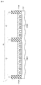
- FIG. it is sectional drawing of the semiconductor device in the sectional line II-II shown in FIG.
- FIG. 1st plan view which shows the bonding region in the semiconductor device which concerns on 2nd modification.
- the 2nd plan view which shows the bonding region in the semiconductor device which concerns on 2nd modification.
- it is a 3rd plan view which shows the bonding region in the semiconductor device which concerns on 2nd modification.
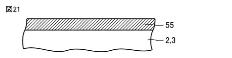
- FIG. In the same embodiment, it is sectional drawing which shows one step of the manufacturing method of a semiconductor device. It is sectional drawing which shows the process performed after the process shown in FIG. 21 in the same embodiment.
- Embodiment 1 The semiconductor device according to the first embodiment will be described. As shown in FIGS. 1 and 2, in the semiconductor device 1, a bonding region 20 to which the metal wiring 13 is bonded is defined on one main surface of the semiconductor substrate 3 (semiconductor device) on which the semiconductor element 2 is formed. There is. As the metal wiring 13, for example, a copper wiring (wire) is connected.
- an insulated gate type bipolar transistor IGBT: Insulated Gate Bipolar Transistor
- MOSFET Metal Oxide Semiconductor Field Effect Transistor
- the semiconductor substrate 3 for example, a Si substrate or a SiC substrate is applied.
- a semiconductor element other than the IGBT and the MOSFET may be formed.
- a GaN substrate may be applied as the semiconductor substrate 3.
- the thickness of the chip as the semiconductor device 1 is, for example, about 50 ⁇ m to 500 ⁇ m.
- Electrodes may be formed on the other main surface (not shown) of the semiconductor substrate 3.
- As the material of the electrode for example, gold (Au), copper (Cu) or nickel (Ni) is applied.
- An adhesion layer, a barrier layer or an antioxidant layer may be formed between the other main surface of the semiconductor substrate 3 and the electrode.
- As a material for the adhesion layer or the like for example, gold (Au), titanium (Ti), titanium nitride (TiN), tungsten (W) or the like is applied.
- the electrode may have a laminated structure of two or more layers. The thickness of the electrode is, for example, about 5 nm to 50 ⁇ m.
- the electrodes are formed, for example, by plating or sputtering.
- the bonding region 20 is defined by the insulating member 11.
- the bonding region 20 defines a first region 21 and a second region 23.
- the first region 21 and the second region 23 are separated by an insulating member 11.
- the area of the first region 21 is set to be larger than the area of the second region 23.
- a first structure 5a (5) having a first uneven portion 6 and a second structure 7a (7) having a second uneven portion 8 are formed.
- the second structure 7a (7) is formed so as to cover the first structure 5a (5).
- a first structure 5b (5) having the first uneven portion 6 and a second structure 7b (7) having the second uneven portion 8 are formed.
- the second structure 7b (7) is formed so as to cover the first structure 5b (5).
- the first structure 5 having the first uneven portion 6 is arranged on one main surface of the semiconductor substrate 3 in an island shape, for example, in a manner in which a plurality of convex portions are separated from each other.
- the first structure 5 may be formed directly on the main surface of the semiconductor substrate 3.
- a layer for adhesion or a layer for electrical connection may be interposed between the first structure 5 and the main surface of the semiconductor substrate 3.
- the material of such a layer for example, titanium (Ti), tungsten (W), nickel (Ni), or an alloy mainly containing these metals is applied. It should be noted that the material is not limited to these materials as long as it is a material capable of achieving adhesion or electrical connectivity.
- a metal such as aluminum (Al), copper (Cu), nickel (Ni), tungsten (W), silicon (Si), an oxide film, or the like is applied.
- the material is not limited to these materials as long as the function as the semiconductor device 1 is not impaired.
- the first uneven portion 6 of the first structure 5 is formed in a form of a dot-shaped convex portion as an example.
- the length (width) of one side of the convex portion of the first uneven portion 6 is, for example, about 1 ⁇ m to 10 ⁇ m.
- the height of the convex portion is, for example, about 0.5 ⁇ m to 5 ⁇ m.
- the distance between the convex portions adjacent to each other is, for example, about 0.5 ⁇ m to 5 ⁇ m.
- the second structure 7 having the second uneven portion 8 is formed of the metal layer 77.
- the metal layer 77 By forming the metal layer 77 so as to cover the first uneven portion 6 of the first structure 5, for example, the metal layer 77 reflects the first uneven portion 6 of the base, and the second uneven portion 8 is formed. It is formed. Therefore, the second uneven portion 8 is also formed in a dot shape.
- the material of the second structure 7 for example, aluminum (Al), copper (Cu), nickel (Ni), cobalt (Co), chromium (Cr) and the like are applied.
- the hardness of the second structure 7 (metal layer 77) is preferably 300 or more as measured by a Vickers hardness tester. When the Vickers hardness is 300 or more, good bonding can be achieved while reducing the load acting during wire bonding.
- the material of the metal layer 77 is not limited to the above-mentioned material as long as the function as the semiconductor device 1 is impaired.
- an antioxidant layer (not shown) may be formed on the surface of the second structure 7 in order to suppress the oxidation of the metal layer 77.
- gold (Au), silver (Ag), palladium (Pg), or an alloy layer of these metals can be applied.
- an organic protective film or the like can also be applied as the antioxidant layer.
- the thickness of the second structure 7 is, for example, about 1 ⁇ m to 50 ⁇ m.
- the thickness of the second structure 7 corresponds to the distance between the upper end portion and the lower end portion of the second structure 7.
- the depth D2 of the dent of the second uneven portion 8 of the second structure 7 is shallower than the depth D1 of the dent of the first uneven portion 6 of the first structure 5 (see FIG. 7).
- the depth of the recess of the second uneven portion 8 is preferably 5 ⁇ m or less, for example.
- the shape of the second uneven portion 8 of the second structure 7 is different from the roughness of the surface of the metal layer 77.
- the depth of the dent of the first uneven portion 6 and the depth of the dent of the second uneven portion 8 have larger values than the surface roughness (Ra) of the metal layer 77 with respect to the average film thickness of the metal layer 77. ..
- Copper wiring includes pure copper or copper alloys. Further, the metal wiring 13 may be a copper wiring in which the outermost surface of the copper wiring is coated with palladium (Pd), aluminum (Al), gold (Au), silver (Ag) or the like.
- the metal wiring 13 is not limited to copper wiring, and for example, aluminum wiring and the like can be applied. Further, as the metal wiring 13, for example, nickel wiring can also be applied.
- a wire is preferable as the shape of the metal wiring 13.
- the thickness ( ⁇ ) of the wire is, for example, about 100 ⁇ m to 500 ⁇ m.
- the shape of the metal wiring 13 may be, for example, a plate-shaped metal wiring 13 or a foil-shaped metal wiring 13 in addition to the wire.
- the metal wiring 13 for example, a copper wire is bonded to the bonding region 20 by ultrasonic waves.
- the portion of the metal wiring 13 is embedded in the recessed region of the second uneven portion 8 in the portion where the metal wiring 13 is joined. If the contact area between the copper wire and the bonding region 20 can be secured while reducing the load acting on the wire bonding, the metal is left in the recessed region of the second uneven portion 8.
- the wiring 13 may be joined.
- the insulating member 11 is formed so as to cover the semiconductor substrate 3 on which the semiconductor element 2 is formed.
- the insulating member 11 is formed so as to reach the semiconductor substrate 3.
- the insulating member 11 defines a bonding region 20. Further, the insulating member 11 defines a first region 21 and a second region 23. The area of the second region 23 is set smaller than the area of the first region 21.
- the shape, material and shape of the insulating member 11 are not particularly limited as long as the function as a semiconductor device is not impaired.
- the insulating member 11 may have a structure in which the insulating member 11 reaches the second structure 7, in addition to the structure formed so as to reach the semiconductor substrate 3. Further, the insulating member 11 may be formed so as to reach the first structure 5.
- the first uneven portion 6 of the first structure 5a and the second uneven portion 8 of the second structure 7 are located.
- the first uneven portion 6 of the first structure 5b and the second uneven portion 8 of the second structure 7 are located.
- the first uneven portion 6 and the second uneven portion 8 may be formed in at least the second region 23 having a small area among the first region 21 and the second region 23.
- the first concavo-convex portion 6 and the second concavo-convex portion 8 are formed in both the first concavo-convex portion 21 and the second concavo-convex portion 23
- the first concavo-convex portion 6 and the second concavo-convex portion 8 have the first concavo-convex portion 21 and the second concavo-convex portion 8.
- the two regions 23 may have the same shape or different shapes from each other.
- the convex portion of the first uneven portion 6 of the first structure 5 is formed periodically, for example.
- the second structure 7 having the second uneven portion 8 is formed so as to cover the first structure 5.
- the second structure 7 may be formed so as to be embedded between the convex portions of the first uneven portion 6, or a partial cavity may be left between the convex portions. It may be formed in.
- the second uneven portion 8 of the second structure 7 may have an uneven shape that reflects the uneven shape of the first uneven portion 6 of the first structure 5, or the first uneven portion 5 of the first structure 5.
- An uneven shape independent of the uneven shape of 1 uneven portion 6 may be used.
- the depth of the dent of the second uneven portion 8 of the second structure 7 is shallower than the depth of the dent of the first uneven portion 6 of the first structure 5.
- the depth of the dent of the second uneven portion 8 is preferably 80% or less of the depth of the dent of the first uneven portion 6.
- the manufacturing process is broadly divided into three first manufacturing processes, a second manufacturing process, and a third manufacturing process.
- first manufacturing step the first structure 5 having the first uneven portion 6 is formed.
- second manufacturing process the second structure 7 having the second uneven portion 8 is formed.
- third manufacturing process metal wiring is joined.
- the first manufacturing process will be explained.
- the semiconductor element 2 and the like are formed on the semiconductor substrate 3 (see FIG. 3).
- the photoresist 51 is applied so as to cover the main surface of the semiconductor substrate 3 on which the semiconductor element 2 and the like are formed.
- the photoresist 51 includes a positive resist and a negative resist. Either positive resist or negative resist may be used as long as the first uneven portion can be patterned as designed.
- the photoresist 51 is subjected to a photoengraving process.
- a photomask corresponding to the pattern of the first structure is set in an exposure apparatus (not shown), and the pattern of the photomask is transferred to the photoresist 51 by irradiating with ultraviolet rays.
- the portion of the photoresist that has not been cured is removed.
- a pattern of the photoresist 51 for forming the first structure is formed.
- a metal layer 55 to be the first structure is formed so as to cover the pattern of the photoresist 51.
- a method for forming the metal layer 55 for example, there is a sputtering method as one of the physical vapor deposition methods (PVD).
- the sputtering method includes a magnetron sputtering method, a vapor deposition method, an ion beam sputtering method and the like. Any sputtering method may be applied as long as the first uneven portion 6 can be formed.
- the first uneven portion 6 can be formed. If possible, any condition may be set.
- Plating methods include electroless plating and electrolytic plating.
- any plating method and conditions may be set as long as the first uneven portion 6 can be formed.
- the seed layer and the adhesion layer For example, there is a physical vapor deposition method or a chemical vapor deposition method (CVD). Any method may be applied as long as the first structure 5 can be formed. From the viewpoint of the configuration of the semiconductor device 1, the sputtering method is desirable as a method for forming the seed layer and the adhesion layer.
- the first structure 5 is formed by an oxide film
- a chemical vapor deposition method as a method for forming the oxide film.
- a silicon oxide film can be formed by using monosilane gas and oxygen.
- the pattern of the photoresist 51 is removed.
- a method for removing the photoresist 51 there is a wet etching process or a dry etching process.
- the etching solution is not particularly limited as long as the photoresist 51 can be removed while maintaining the shape of the first uneven portion 6. In this way, the first manufacturing process is completed.
- the metal layer 77 is formed so as to cover the first structure 5.
- the thickness of the metal layer 77 is set to a thickness that reflects the shape of the base. Since the first structure 5 has the first uneven portion 6, the metal layer 77 is formed with the second uneven portion 8 reflecting the shape of the first uneven portion 6 without any additional processing. Will be.
- the depth D2 of the dent of the second uneven portion 8 of the second structure 7 is formed to be shallower than the depth D1 of the dent of the first uneven portion 6 of the first structure 5.
- the case where the shape of the base is not reflected on the metal layer 77 will be described later as a modification. In this way, the second manufacturing process is completed.
- a process of forming the insulating member 11 is performed in the bonding region 20.
- the surface of the semiconductor substrate 3 located in the region where the insulating member should be arranged is exposed by subjecting the metal layer 77 or the like to a photoplate making process and an etching process.
- the insulating member 11 is formed so as to cover the semiconductor substrate 3, for example, by a chemical vapor deposition method.
- the pattern of the photoresist 52 is formed by performing a photoplate making process. The photoresist 52 defines the bonding region 20 and is formed in a pattern that partitions the first region 21 and the second region 23.
- the second structure 7 is exposed by subjecting the insulating member 11 to, for example, a dry etching process using the pattern of the photoresist 52 as an etching mask. After that, the photoresist 52 is removed. In this way, the insulating member 11 that defines the bonding region 20 and the first region 21 and the second region 23 is patterned.
- the metal wiring 13 (13a, 13b) is joined to the bonding region 20.
- the copper wire is joined to the second structure 7a (7) of the first region 21 by ultrasonic waves.
- the metal wiring 13b the copper wire is joined to the second structure 7b (7) of the second region 23 by ultrasonic waves.
- the metal wiring 13a of the copper wire is joined to the second structure 7a of the first region 21, and the metal wiring 13b of the copper wire is connected to the second structure 7b of the second region 23. Is joined to. In this way, the third manufacturing process is completed, and the main part of the semiconductor device 1 is completed.
- the copper wire as the metal wiring 13 is joined to the second structure 7 having the second uneven portion 8 formed in the bonding region 20. Therefore, when the copper wire is joined to the second structure 7 by ultrasonic waves, the energy of the ultrasonic waves is dispersed by the second uneven portion 8. Further, the second structure 7 in which the second uneven portion 8 is formed is laminated on the first structure 5 in which the first uneven portion 6 is formed. This effectively disperses the ultrasonic energy. Further, the contact area between the copper wire and the second structure 7 (bonding region 20) is increased, and the frictional force required for joining the copper wire can be effectively obtained.
- the copper wire which requires a larger ultrasonic energy than the case of joining the aluminum wire, can be joined without giving a large load to the bonding region 20 and the like.
- the insulating member 11 defining the bonding region 20 is formed so as to reach the semiconductor substrate 3, it is possible to suppress the influence of ultrasonic waves from extending to the outside of the bonding region 20.
- Patent Document 1 In order to join a copper wire, there is a method of forming a copper film having a thickness of about 30 ⁇ m in advance in the bonding region (Patent Document 1). Compared with such a method, the step of forming the copper film while controlling the thickness of the copper film becomes unnecessary, and the time required for manufacturing can be reduced. In addition, it can contribute to the reduction of production cost.
- Patent Document 2 there is a method in which the bonding region to which the metal wire is bonded has an uneven shape.
- Patent Document 2 a method in which the bonding region to which the metal wire is bonded has an uneven shape.
- the depth of the dent of the second uneven portion 8 is set to 80% or less of the depth of the dent of the first uneven portion 6, for example, as a metal wiring 13.
- the contact area between the copper wire and the second structure 7 (bonding region) is surely secured. As a result, the copper wire can be firmly bonded to the bonding region 20.
- the area of the gate pad electrically connected to the gate electrode such as an IGBT is relatively small, and the surface of the gate pad is flat.
- the second region 23 having a small area is used as a gate pad, and the second structure 7 of the second region 23 is made of metal.
- a copper wire as wiring 13 can be joined. As a result, the copper wires in the gate pad are surely joined, and the reliability of the semiconductor device 1 can be improved.
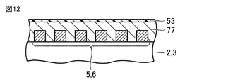
- the second uneven portion 8 is intentionally formed on the metal layer 77 (see FIG. 7) to be the second structure.
- the metal layer 77 may have a second uneven portion 8 having a pattern different from that of the first uneven portion 6 of the first structure 5.
- a metal layer 77 to be a second structure is formed so as to cover the first structure 5.
- the surface of the metal layer 77 is flat.
- the photoresist 53 is applied so as to cover the metal layer 77.
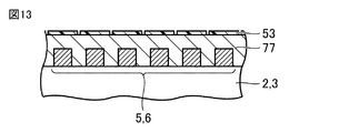
- a pattern of the photoresist 53 for forming the second structure 7 having the second uneven portion 8 is formed by performing a photoengraving process.
- the metal layer 77 is subjected to, for example, a dry etching process using the pattern of the photoresist 53 as an etching mask to form the second structure 7 having the second uneven portion 8. ..
- the photoresist 53 is removed. Then, through the same steps as those shown in FIGS. 8 to 10, the semiconductor device 1 in which the metal wiring 13 is bonded to the bonding region 20 is manufactured (see FIG. 2).
- the second uneven portion 8 can be formed on the metal layer 77, and the metal wiring 13 is firmly formed in the bonding region 20. Can be joined. Further, it is possible to form the second uneven portion 8 (second structure 7) having an appropriate depth and pattern corresponding to the bonding conditions of the metal wiring 13 to the bonding region 20. As a result, the metal wiring 13 can be joined to the second structure 7 having the second uneven portion 8 that is optimal for various joining conditions.
- the first concavo-convex portion 6 is formed in a manner of forming a dot-shaped convex portion
- the second concavo-convex portion 8 is a dot-shaped convex portion reflecting the dot-shaped first concavo-convex portion 6.
- the case where is formed has been described as an example.
- variations of the patterns of the convex portions or the concave portions of the first uneven portion 6 and the second uneven portion 8 will be described.
- the first uneven portion 6 and the second uneven portion 8 may have, for example, a striped pattern. Further, as shown in FIG. 17, the first uneven portion 6 and the second uneven portion 8 may have, for example, a meandering pattern. Further, as shown in FIG. 18, the first uneven portion 6 and the second uneven portion 8 may have, for example, a track-shaped (elliptical) pattern.
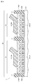
- the intermediate structure is formed to improve the adhesion between the first structure 5 and the second structure 7. Further, the intermediate structure is formed in order to suppress the diffusion of the respective materials between the first structure 5 and the second structure 7.
- the intermediate structure 9 is interposed between the first structure 5 and the second structure 7.
- the intermediate structure 9a is interposed between the first structure 5a and the second structure 7a.
- the intermediate structure 9b is interposed between the first structure 5b and the second structure 7b.
- the intermediate structure 9 may be a single layer or a plurality of layers.
- Materials of the intermediate structure 9 include, for example, aluminum (Al), copper (Cu), nickel (Ni), tungsten (W), cobalt (Co), chromium (Cr) or titanium (Ti).
- Al aluminum
- Cu copper
- Ni nickel
- W tungsten
- Co cobalt
- Cr chromium
- Ti titanium
- the characteristics such as density, surface roughness, and electric conductivity are not particularly limited.
- the shape of the intermediate structure 9 is not particularly limited as long as the ultrasonic energy is effectively dispersed and the frictional force required for joining the copper wires can be effectively obtained.
- the intermediate structure 9 may not have an uneven shape.
- the intermediate structure 9 may be formed so as to be embedded between the convex portions of the first uneven portion 6, or a partial cavity is left between the convex portions. It may be formed as follows.
- the second uneven portion 8 is formed through the same steps as those shown in FIGS. 11 to 15 described above.
- the second structure 7 having can be formed.
- the uneven shape may be a concave-convex shape that reflects the shape of the first uneven portion 6, and is different from the first uneven portion 6. It may be an uneven shape having a pattern. Further, the depth of the concave-convex shape of the intermediate structure 9 is not particularly limited.
- the intermediate structure 9 has an uneven shape
- the metal layer 77 can reflect the shape of the base when forming the second structure 7
- the second uneven portion is formed on the metal layer 77. No additional step of forming 8 is required.
- the metal wiring 13 can be more firmly bonded to the bonding region 20 by forming the intermediate structure 9 for improving the adhesion and the like.
- the gate pad and the gate electrode are different from each other. Since it is electrically connected by the wiring (not shown), an insulating film can be applied as the intermediate structure 9.
- Embodiment 2 In the first embodiment, the case where the first structure 5 is arranged on the main surface of the semiconductor substrate 3 in such a manner that a plurality of convex portions are separated from each other has been described. Here, an example of a semiconductor device provided with the continuous film-shaped first structure 5 will be described.
- a continuous film-shaped first structure 5 having the first uneven portion 6 is formed in the bonding region 20 of the semiconductor device 1.
- the first structure 5 includes a portion extending in a film shape on the surface of the semiconductor substrate 3 and a portion protruding from the film-like portion.
- the height (thickness of the first structure 5) between the lower surface of the film-like portion and the upper surface of the protruding portion is, for example, about 1 ⁇ m to 50 ⁇ m.
- a first structure 5a having a first uneven portion 6 and a second structure 7a having a second uneven portion 8 are formed.
- the second structure 7a is formed so as to cover the film-like first structure 5a.
- a first structure 5b having a first uneven portion 6 and a second structure 7b having a second uneven portion 8 are formed.
- the second structure 7b is formed so as to cover the film-like first structure 5b.
- the first structure 5 can be formed through the same steps as those shown in FIGS. 11 to 15.
- a metal layer 55 as a first structure is formed on one main surface of the semiconductor substrate 3.
- the photoresist 54 is applied so as to cover the metal layer 55.
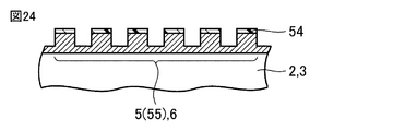
- FIG. 23 by performing a photoengraving process, a pattern of the photoresist 54 for forming the first structure 5 having the first uneven portion 6 is formed.
- the metal layer 55 is subjected to, for example, a dry etching process using the pattern of the photoresist 54 as an etching mask, and the etching process is stopped before the surface of the semiconductor substrate 3 is exposed.
- a continuous film-like first structure 5 having the first uneven portion 6 is formed.
- the photoresist 54 is removed. Then, through the same steps as those shown in FIGS. 7 to 10, the semiconductor device 1 in which the metal wiring 13 is bonded to the bonding region 20 is manufactured (see FIG. 20).
- the energy of the ultrasonic waves is dispersed by the second uneven portion 8. Further, the second structure 7 in which the second uneven portion 8 is formed is laminated on the first structure 5 in which the first uneven portion 6 is formed.
- the first structure 5 having the first uneven portion 6 is formed in a continuous film shape. As a result, it is possible to suppress that the ultrasonic energy stored in the concave portion of the first uneven portion 6 directly affects the semiconductor substrate 3 (semiconductor device 1), and it is possible to prevent damage to the semiconductor device 1. can.
- Embodiment 3 Here, variations of the first structure 5 in the bonding region 20 will be described.
- the semiconductor device 1 according to the first example or the semiconductor device 1 according to the second example described above is manufactured as follows. First, after the semiconductor element 2 and the like are formed on the semiconductor substrate 3, the same steps as those shown in FIGS. 3 to 6 are applied to one of the first region 21 and the second region 23 in the bonding region 20. The first structure 5 having the first uneven portion 6 in such a manner that the plurality of convex portions are separated from each other is formed.
- a continuous film-like first structure 5 having the first uneven portion 6 is subjected to the same steps as those shown in FIGS. 21 to 25. Is formed. After the first structure 5 is formed, the semiconductor device 1 according to the first example or the semiconductor device 1 according to the second example is completed through the same steps as those shown in FIGS. 7 to 10.
- the first structure 5 has a first uneven portion 6 in which a plurality of convex portions are separated from each other. 1 structure 5 and a continuous film-like first structure 5 having a first uneven portion 6 are mixed.
- the first structure 5 having the first uneven portion 6 in which a plurality of convex portions are separated from each other is the first. 1 It is possible to suppress the energy of ultrasonic waves stored in the concave portions of the concave-convex portion 6 from directly affecting the semiconductor substrate 3 (semiconductor device 1). As a result, the choices (range) of the joining conditions such as the energy by ultrasonic waves when joining the metal wiring 13 are increased, and the structural design corresponding to the function of the semiconductor device becomes possible.
- Embodiment 4 the semiconductor device 1 including the bonding region 20 including one region as the bonding region 20 will be described.
- the bonding region 20 comprises one region 25.
- One region 25 is defined by the insulating member 11.
- a continuous film-like first structure 5 having the first uneven portion 6 is formed in one region 25, as the first structure 5.
- a second structure 7 having a second uneven portion 8 is formed so as to cover the first structure 5.
- the bonding region 20 is composed of one region 25.
- One region 25 is defined by the insulating member 11.
- the first structure 5 arranged on the main surface of the semiconductor substrate 3 is formed in such a manner that a plurality of convex portions of the first uneven portion 6 are separated from each other.
- a second structure 7 having a second uneven portion 8 is formed so as to cover the first structure 5.
- the bonding region 20 is not divided into a plurality of regions, but is formed from one region 25. This makes it possible to form a bonding region on the surface of a diode (chip), for example, as a semiconductor element that generally does not require a plurality of electrode pads. As a result, the degree of freedom in the structural design of the semiconductor device 1 can be increased.
- Embodiment 5 a power conversion device to which the semiconductor device described in the above-described first to fourth embodiments will be described will be described.
- the present disclosure is not limited to a specific power conversion device, the case where the present disclosure is applied to a three-phase inverter will be described below as the fifth embodiment.
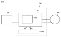
- FIG. 30 is a block diagram showing a configuration of a power conversion system to which the power conversion device according to the present embodiment is applied.
- the power conversion system shown in FIG. 30 includes a power supply 100, a power conversion device 200, and a load 300.
- the power supply 100 is a DC power supply, and supplies DC power to the power conversion device 200.
- the power supply 100 can be configured by various types, for example, a DC system, a solar cell, and a storage battery. Further, it may be configured by a rectifier circuit or an AC / DC converter connected to an AC system. Further, the power supply 100 may be configured by a DC / DC converter that converts the DC power output from the DC system into a predetermined power.
- the power conversion device 200 is a three-phase inverter connected between the power supply 100 and the load 300, converts the DC power supplied from the power supply 100 into AC power, and supplies the AC power to the load 300. As shown in FIG. 30, the power conversion device 200 has a main conversion circuit 201 that converts DC power into AC power and outputs it, and a control circuit 203 that outputs a control signal for controlling the main conversion circuit 201 to the main conversion circuit 201. And have.
- the load 300 is a three-phase electric motor driven by AC power supplied from the power conversion device 200.
- the load 300 is not limited to a specific application, and is an electric motor mounted on various electric devices.
- the load 300 is used as an electric motor for a hybrid vehicle, an electric vehicle, a railroad vehicle, an elevator, or an air conditioner.
- the main conversion circuit 201 includes a switching element and a freewheeling diode (not shown). When the switching element switches, the DC power supplied from the power supply 100 is converted into AC power and supplied to the load 300.
- the main conversion circuit 201 is a two-level three-phase full bridge circuit, and has six switching elements and each switching element. It can consist of six anti-parallel freewheeling diodes.
- each switching element and each freewheeling diode of the main conversion circuit 201 is a switching element or a freewheeling diode included in the semiconductor device 202 corresponding to the semiconductor device 1 according to at least one of the above-described embodiments 1 to 3. ..
- the six switching elements form an upper and lower arm connected in series for each of the two switching elements, and each upper and lower arm constitutes each phase (U phase, V phase, W phase) of the full bridge circuit. Then, the output terminals of each upper and lower arm, that is, the three output terminals of the main conversion circuit 201 are connected to the load 300.
- the main conversion circuit 201 includes a drive circuit (not shown) for driving each switching element, but the drive circuit may be built in the semiconductor device 202 or may be a drive circuit separate from the semiconductor device 202. It may be configured to include.
- the drive circuit generates a drive signal for driving the switching element of the main conversion circuit 201 and supplies it to the control electrode of the switching element of the main conversion circuit 201. Specifically, according to the control signal from the control circuit 203 described later, a drive signal for turning on the switching element and a drive signal for turning off the switching element are output to the control electrode of each switching element.
- the drive signal When the switching element is kept on, the drive signal is a voltage signal (on signal) equal to or higher than the threshold voltage of the switching element, and when the switching element is kept off, the drive signal is a voltage equal to or lower than the threshold voltage of the switching element. It becomes a signal (off signal).
- the control circuit 203 controls the switching element of the main conversion circuit 201 so that the desired power is supplied to the load 300. Specifically, the time (on time) in which each switching element of the main conversion circuit 201 should be in the on state is calculated based on the electric power to be supplied to the load 300.
- the main conversion circuit 201 can be controlled by PWM control that modulates the on-time of the switching element according to the voltage to be output. Then, a control command (control signal) is output to the drive circuit provided in the main conversion circuit 201 so that an on signal is output to the switching element that should be turned on at each time point and an off signal is output to the switching element that should be turned off. Is output.
- the drive circuit outputs an on signal or an off signal as a drive signal to the control electrode of each switching element according to this control signal.
- the semiconductor device 1 according to the first to fourth embodiments is applied as the semiconductor device 202 constituting the main conversion circuit 201.
- the metal wiring 13 copper wires and the like can be firmly and satisfactorily bonded to the bonding region 20.
- the reliability of the power converter 200 can be improved.
- the present disclosure is not limited to this, and can be applied to various power conversion devices.
- a two-level power conversion device is used, but a three-level or multi-level power conversion device may be used, and when power is supplied to a single-phase load, a single-phase inverter is used. Disclosure may be applied. Further, when supplying electric power to a DC load or the like, the present disclosure can be applied to a DC / DC converter or an AC / DC converter.
- the power conversion device to which the present disclosure is applied is not limited to the case where the above-mentioned load is an electric motor, and is, for example, as a power supply device for an electric discharge machine, a laser machine, an induction heating cooker, or a contactless power supply system. It can also be used, and can also be used as a power conditioner for a photovoltaic power generation system, a power storage system, or the like.
- the semiconductor devices 1 described in each embodiment can be combined in various ways as needed.
- the present disclosure is effectively used for a semiconductor device for joining a metal wiring to a bonding region.
- 1 Semiconductor device 2 Semiconductor element, 3 Semiconductor substrate, 5, 5a, 5b 1st structure, 6 1st uneven part, 7, 7a, 7b 2nd structure, 8 2nd uneven part, 9, 9a, 9b intermediate Structure, 11 insulating member, 13, 13a, 13b metal wiring, 20 bonding area, 21 first area, 23 second area, 25 one area, 51, 52, 53, 54 resist, 55, 77 metal layer, 100 power supply, 200 power conversion device, 201 main conversion circuit, 202 semiconductor module, 203 control circuit, 300 load.
Landscapes
- Internal Circuitry In Semiconductor Integrated Circuit Devices (AREA)
- Engineering & Computer Science (AREA)
- Manufacturing & Machinery (AREA)
Priority Applications (5)
| Application Number | Priority Date | Filing Date | Title |
|---|---|---|---|
| PCT/JP2020/021175 WO2021240748A1 (ja) | 2020-05-28 | 2020-05-28 | 半導体装置およびその製造方法ならびに電力変換装置 |
| US17/913,442 US12588539B2 (en) | 2020-05-28 | 2020-05-28 | Semiconductor device, method for manufacturing same, and electric power converter |
| JP2022527416A JP7391210B2 (ja) | 2020-05-28 | 2020-05-28 | 半導体装置およびその製造方法ならびに電力変換装置 |
| CN202080101224.5A CN115699267B (zh) | 2020-05-28 | 2020-05-28 | 半导体装置及其制造方法以及电力变换装置 |
| DE112020007244.4T DE112020007244T5 (de) | 2020-05-28 | 2020-05-28 | Halbleitereinrichtung, verfahren zum herstellen derselben, sowie elektrischer stromrichter |
Applications Claiming Priority (1)
| Application Number | Priority Date | Filing Date | Title |
|---|---|---|---|
| PCT/JP2020/021175 WO2021240748A1 (ja) | 2020-05-28 | 2020-05-28 | 半導体装置およびその製造方法ならびに電力変換装置 |
Publications (1)
| Publication Number | Publication Date |
|---|---|
| WO2021240748A1 true WO2021240748A1 (ja) | 2021-12-02 |
Family
ID=78723199
Family Applications (1)
| Application Number | Title | Priority Date | Filing Date |
|---|---|---|---|
| PCT/JP2020/021175 Ceased WO2021240748A1 (ja) | 2020-05-28 | 2020-05-28 | 半導体装置およびその製造方法ならびに電力変換装置 |
Country Status (5)
| Country | Link |
|---|---|
| US (1) | US12588539B2 (https=) |
| JP (1) | JP7391210B2 (https=) |
| CN (1) | CN115699267B (https=) |
| DE (1) | DE112020007244T5 (https=) |
| WO (1) | WO2021240748A1 (https=) |
Citations (7)
| Publication number | Priority date | Publication date | Assignee | Title |
|---|---|---|---|---|
| JPS6310551U (https=) * | 1986-07-09 | 1988-01-23 | ||
| JPS6364035U (https=) * | 1986-10-16 | 1988-04-27 | ||
| JPH04348047A (ja) * | 1991-05-24 | 1992-12-03 | Mitsubishi Electric Corp | 半導体集積回路電極 |
| JPH0543544U (ja) * | 1991-11-12 | 1993-06-11 | 日本無線株式会社 | 電子素子の接続端子構造 |
| JP2013080809A (ja) * | 2011-10-04 | 2013-05-02 | Panasonic Corp | 半導体装置 |
| JP2014027048A (ja) * | 2012-07-25 | 2014-02-06 | Renesas Electronics Corp | 半導体ウェハ及び半導体装置の製造方法 |
| JP2020043154A (ja) * | 2018-09-07 | 2020-03-19 | 三菱電機株式会社 | 半導体装置及びその製造方法、並びに、電力変換装置 |
Family Cites Families (10)
| Publication number | Priority date | Publication date | Assignee | Title |
|---|---|---|---|---|
| JPH0225045A (ja) | 1988-07-13 | 1990-01-26 | Oki Electric Ind Co Ltd | 半導体装置 |
| JP4674522B2 (ja) * | 2004-11-11 | 2011-04-20 | 株式会社デンソー | 半導体装置 |
| JP4645398B2 (ja) * | 2005-10-04 | 2011-03-09 | 株式会社デンソー | 半導体装置およびその製造方法 |
| JP5054755B2 (ja) * | 2009-12-28 | 2012-10-24 | 株式会社日立製作所 | 半導体装置 |
| KR101933015B1 (ko) * | 2012-04-19 | 2018-12-27 | 삼성전자주식회사 | 반도체 장치의 패드 구조물, 그의 제조 방법 및 패드 구조물을 포함하는 반도체 패키지 |
| KR101960686B1 (ko) * | 2012-08-10 | 2019-03-21 | 삼성전자주식회사 | 반도체 장치 및 이의 제조 방법 |
| JP6068425B2 (ja) | 2014-12-11 | 2017-01-25 | 株式会社神戸製鋼所 | 電極構造 |
| JP6650723B2 (ja) * | 2015-10-16 | 2020-02-19 | 新光電気工業株式会社 | リードフレーム及びその製造方法、半導体装置 |
| WO2018207656A1 (ja) * | 2017-05-11 | 2018-11-15 | 三菱電機株式会社 | パワーモジュール、電力変換装置、およびパワーモジュールの製造方法 |
| CN110832628A (zh) * | 2017-07-07 | 2020-02-21 | 三菱电机株式会社 | 半导体装置、以及半导体装置的制造方法 |
-
2020
- 2020-05-28 CN CN202080101224.5A patent/CN115699267B/zh active Active
- 2020-05-28 JP JP2022527416A patent/JP7391210B2/ja active Active
- 2020-05-28 DE DE112020007244.4T patent/DE112020007244T5/de active Pending
- 2020-05-28 WO PCT/JP2020/021175 patent/WO2021240748A1/ja not_active Ceased
- 2020-05-28 US US17/913,442 patent/US12588539B2/en active Active
Patent Citations (7)
| Publication number | Priority date | Publication date | Assignee | Title |
|---|---|---|---|---|
| JPS6310551U (https=) * | 1986-07-09 | 1988-01-23 | ||
| JPS6364035U (https=) * | 1986-10-16 | 1988-04-27 | ||
| JPH04348047A (ja) * | 1991-05-24 | 1992-12-03 | Mitsubishi Electric Corp | 半導体集積回路電極 |
| JPH0543544U (ja) * | 1991-11-12 | 1993-06-11 | 日本無線株式会社 | 電子素子の接続端子構造 |
| JP2013080809A (ja) * | 2011-10-04 | 2013-05-02 | Panasonic Corp | 半導体装置 |
| JP2014027048A (ja) * | 2012-07-25 | 2014-02-06 | Renesas Electronics Corp | 半導体ウェハ及び半導体装置の製造方法 |
| JP2020043154A (ja) * | 2018-09-07 | 2020-03-19 | 三菱電機株式会社 | 半導体装置及びその製造方法、並びに、電力変換装置 |
Also Published As
| Publication number | Publication date |
|---|---|
| JPWO2021240748A1 (https=) | 2021-12-02 |
| CN115699267A (zh) | 2023-02-03 |
| US12588539B2 (en) | 2026-03-24 |
| CN115699267B (zh) | 2025-05-09 |
| JP7391210B2 (ja) | 2023-12-04 |
| DE112020007244T5 (de) | 2023-03-09 |
| US20230197649A1 (en) | 2023-06-22 |
Similar Documents
| Publication | Publication Date | Title |
|---|---|---|
| JP6987031B2 (ja) | 電力用半導体装置及びその製造方法、並びに、電力変換装置 | |
| US20080157310A1 (en) | Power device package | |
| JP6927437B1 (ja) | パワーモジュールおよび電力変換装置 | |
| JP6826665B2 (ja) | 半導体装置、半導体装置の製造方法及び電力変換装置 | |
| JP7443926B2 (ja) | 半導体装置およびその製造方法 | |
| JP2017220663A (ja) | 電子部品パッケージおよびその製造方法 | |
| JP7584620B2 (ja) | 半導体素子の製造方法 | |
| JP6892023B1 (ja) | 半導体装置、半導体装置の製造方法および電力変換装置 | |
| JP2014053403A (ja) | パワーモジュール半導体装置 | |
| JP2019102535A (ja) | 半導体モジュール、その製造方法及び電力変換装置 | |
| CN111788694B (zh) | 半导体元件、半导体装置、电力变换装置以及半导体元件的制造方法 | |
| JP7391210B2 (ja) | 半導体装置およびその製造方法ならびに電力変換装置 | |
| JP7555486B2 (ja) | パワー半導体装置及び電力変換装置 | |
| JP2022041649A (ja) | 素子パッケージおよび半導体装置 | |
| JP7531624B2 (ja) | 半導体装置、電力変換装置および半導体装置の製造方法 | |
| JP2021061332A (ja) | 半導体装置および電力変換装置 | |
| WO2020240790A1 (ja) | パワー半導体モジュール及び電力変換装置 | |
| WO2018189948A1 (ja) | 半導体モジュール、半導体モジュールの製造方法および電力変換装置 | |
| JP7088421B1 (ja) | 半導体装置および電力変換装置 | |
| JP2023013642A (ja) | 半導体装置 | |
| CN121219825A (zh) | 半导体元件、半导体装置、电力转换装置以及半导体元件的制造方法 | |
| JP7438466B1 (ja) | 半導体装置及びその製造方法並びに電力変換装置 | |
| JP2022007599A (ja) | 半導体装置 | |
| JP7686143B2 (ja) | 半導体装置、電力変換装置および半導体装置の製造方法 | |
| JP7101890B2 (ja) | 半導体装置、電力変換装置および半導体装置の製造方法 |
Legal Events
| Date | Code | Title | Description |
|---|---|---|---|
| 121 | Ep: the epo has been informed by wipo that ep was designated in this application |
Ref document number: 20938085 Country of ref document: EP Kind code of ref document: A1 |
|
| ENP | Entry into the national phase |
Ref document number: 2022527416 Country of ref document: JP Kind code of ref document: A |
|
| 122 | Ep: pct application non-entry in european phase |
Ref document number: 20938085 Country of ref document: EP Kind code of ref document: A1 |
|
| WWG | Wipo information: grant in national office |
Ref document number: 202080101224.5 Country of ref document: CN |
|
| WWG | Wipo information: grant in national office |
Ref document number: 17913442 Country of ref document: US |