JP7391210B2 - 半導体装置およびその製造方法ならびに電力変換装置 - Google Patents
半導体装置およびその製造方法ならびに電力変換装置 Download PDFInfo
- Publication number
- JP7391210B2 JP7391210B2 JP2022527416A JP2022527416A JP7391210B2 JP 7391210 B2 JP7391210 B2 JP 7391210B2 JP 2022527416 A JP2022527416 A JP 2022527416A JP 2022527416 A JP2022527416 A JP 2022527416A JP 7391210 B2 JP7391210 B2 JP 7391210B2
- Authority
- JP
- Japan
- Prior art keywords
- uneven portion
- semiconductor device
- region
- forming
- semiconductor substrate
- Prior art date
- Legal status (The legal status is an assumption and is not a legal conclusion. Google has not performed a legal analysis and makes no representation as to the accuracy of the status listed.)
- Active
Links
- 239000004065 semiconductor Substances 0.000 title claims description 170
- 238000006243 chemical reaction Methods 0.000 title claims description 47
- 238000004519 manufacturing process Methods 0.000 title claims description 29
- 229910052751 metal Inorganic materials 0.000 claims description 94
- 239000002184 metal Substances 0.000 claims description 94
- 239000000758 substrate Substances 0.000 claims description 49
- 238000000034 method Methods 0.000 claims description 40
- RYGMFSIKBFXOCR-UHFFFAOYSA-N Copper Chemical compound [Cu] RYGMFSIKBFXOCR-UHFFFAOYSA-N 0.000 claims description 36
- 239000010949 copper Substances 0.000 claims description 25
- 229910052802 copper Inorganic materials 0.000 claims description 21
- PXHVJJICTQNCMI-UHFFFAOYSA-N Nickel Chemical compound [Ni] PXHVJJICTQNCMI-UHFFFAOYSA-N 0.000 claims description 20
- 229910052759 nickel Inorganic materials 0.000 claims description 7
- 239000011651 chromium Substances 0.000 claims description 6
- 238000012545 processing Methods 0.000 claims description 4
- VYZAMTAEIAYCRO-UHFFFAOYSA-N Chromium Chemical compound [Cr] VYZAMTAEIAYCRO-UHFFFAOYSA-N 0.000 claims description 3
- 229910052804 chromium Inorganic materials 0.000 claims description 3
- 229910017052 cobalt Inorganic materials 0.000 claims description 3
- 239000010941 cobalt Substances 0.000 claims description 3
- GUTLYIVDDKVIGB-UHFFFAOYSA-N cobalt atom Chemical compound [Co] GUTLYIVDDKVIGB-UHFFFAOYSA-N 0.000 claims description 3
- 238000005304 joining Methods 0.000 claims description 3
- 239000010410 layer Substances 0.000 description 51
- 229920002120 photoresistant polymer Polymers 0.000 description 27
- 239000000463 material Substances 0.000 description 19
- 238000012986 modification Methods 0.000 description 11
- 230000004048 modification Effects 0.000 description 11
- 239000010931 gold Substances 0.000 description 8
- 229910052782 aluminium Inorganic materials 0.000 description 7
- XAGFODPZIPBFFR-UHFFFAOYSA-N aluminium Chemical compound [Al] XAGFODPZIPBFFR-UHFFFAOYSA-N 0.000 description 7
- 238000004544 sputter deposition Methods 0.000 description 7
- 238000005530 etching Methods 0.000 description 6
- 238000007747 plating Methods 0.000 description 6
- 239000010936 titanium Substances 0.000 description 6
- KDLHZDBZIXYQEI-UHFFFAOYSA-N Palladium Chemical compound [Pd] KDLHZDBZIXYQEI-UHFFFAOYSA-N 0.000 description 5
- 238000000206 photolithography Methods 0.000 description 5
- 238000005229 chemical vapour deposition Methods 0.000 description 4
- 238000001312 dry etching Methods 0.000 description 4
- PCHJSUWPFVWCPO-UHFFFAOYSA-N gold Chemical compound [Au] PCHJSUWPFVWCPO-UHFFFAOYSA-N 0.000 description 4
- 229910052737 gold Inorganic materials 0.000 description 4
- WFKWXMTUELFFGS-UHFFFAOYSA-N tungsten Chemical compound [W] WFKWXMTUELFFGS-UHFFFAOYSA-N 0.000 description 4
- 229910052721 tungsten Inorganic materials 0.000 description 4
- 239000010937 tungsten Substances 0.000 description 4
- RTAQQCXQSZGOHL-UHFFFAOYSA-N Titanium Chemical compound [Ti] RTAQQCXQSZGOHL-UHFFFAOYSA-N 0.000 description 3
- 229910045601 alloy Inorganic materials 0.000 description 3
- 239000000956 alloy Substances 0.000 description 3
- 230000001771 impaired effect Effects 0.000 description 3
- 150000002739 metals Chemical class 0.000 description 3
- 238000005240 physical vapour deposition Methods 0.000 description 3
- 230000003746 surface roughness Effects 0.000 description 3
- 229910052719 titanium Inorganic materials 0.000 description 3
- BQCADISMDOOEFD-UHFFFAOYSA-N Silver Chemical compound [Ag] BQCADISMDOOEFD-UHFFFAOYSA-N 0.000 description 2
- 239000012790 adhesive layer Substances 0.000 description 2
- 230000003064 anti-oxidating effect Effects 0.000 description 2
- 238000013461 design Methods 0.000 description 2
- 238000010586 diagram Methods 0.000 description 2
- 238000009792 diffusion process Methods 0.000 description 2
- 230000000694 effects Effects 0.000 description 2
- 238000009713 electroplating Methods 0.000 description 2
- -1 for example Substances 0.000 description 2
- 238000010438 heat treatment Methods 0.000 description 2
- 229910052763 palladium Inorganic materials 0.000 description 2
- 229910052709 silver Inorganic materials 0.000 description 2
- 239000004332 silver Substances 0.000 description 2
- 238000003860 storage Methods 0.000 description 2
- 238000001039 wet etching Methods 0.000 description 2
- 229910000881 Cu alloy Inorganic materials 0.000 description 1
- JMASRVWKEDWRBT-UHFFFAOYSA-N Gallium nitride Chemical compound [Ga]#N JMASRVWKEDWRBT-UHFFFAOYSA-N 0.000 description 1
- BLRPTPMANUNPDV-UHFFFAOYSA-N Silane Chemical compound [SiH4] BLRPTPMANUNPDV-UHFFFAOYSA-N 0.000 description 1
- VYPSYNLAJGMNEJ-UHFFFAOYSA-N Silicium dioxide Chemical compound O=[Si]=O VYPSYNLAJGMNEJ-UHFFFAOYSA-N 0.000 description 1
- XUIMIQQOPSSXEZ-UHFFFAOYSA-N Silicon Chemical compound [Si] XUIMIQQOPSSXEZ-UHFFFAOYSA-N 0.000 description 1
- NRTOMJZYCJJWKI-UHFFFAOYSA-N Titanium nitride Chemical compound [Ti]#N NRTOMJZYCJJWKI-UHFFFAOYSA-N 0.000 description 1
- 239000002313 adhesive film Substances 0.000 description 1
- 239000003963 antioxidant agent Substances 0.000 description 1
- 230000003078 antioxidant effect Effects 0.000 description 1
- QVGXLLKOCUKJST-UHFFFAOYSA-N atomic oxygen Chemical compound [O] QVGXLLKOCUKJST-UHFFFAOYSA-N 0.000 description 1
- 230000004888 barrier function Effects 0.000 description 1
- 230000015572 biosynthetic process Effects 0.000 description 1
- 238000011161 development Methods 0.000 description 1
- 238000007772 electroless plating Methods 0.000 description 1
- 230000005669 field effect Effects 0.000 description 1
- 239000007789 gas Substances 0.000 description 1
- 230000006698 induction Effects 0.000 description 1
- 238000001659 ion-beam spectroscopy Methods 0.000 description 1
- 230000001678 irradiating effect Effects 0.000 description 1
- 238000001755 magnetron sputter deposition Methods 0.000 description 1
- 230000003647 oxidation Effects 0.000 description 1
- 238000007254 oxidation reaction Methods 0.000 description 1
- 239000001301 oxygen Substances 0.000 description 1
- 229910052760 oxygen Inorganic materials 0.000 description 1
- 238000005192 partition Methods 0.000 description 1
- 238000010248 power generation Methods 0.000 description 1
- 230000001681 protective effect Effects 0.000 description 1
- 229910052710 silicon Inorganic materials 0.000 description 1
- 239000010703 silicon Substances 0.000 description 1
- 229910052814 silicon oxide Inorganic materials 0.000 description 1
- 239000002356 single layer Substances 0.000 description 1
- 238000007740 vapor deposition Methods 0.000 description 1
Images


Classifications
-
- H—ELECTRICITY
- H01—ELECTRIC ELEMENTS
- H01L—SEMICONDUCTOR DEVICES NOT COVERED BY CLASS H10
- H01L24/00—Arrangements for connecting or disconnecting semiconductor or solid-state bodies; Methods or apparatus related thereto
- H01L24/01—Means for bonding being attached to, or being formed on, the surface to be connected, e.g. chip-to-package, die-attach, "first-level" interconnects; Manufacturing methods related thereto
- H01L24/02—Bonding areas ; Manufacturing methods related thereto
- H01L24/04—Structure, shape, material or disposition of the bonding areas prior to the connecting process
- H01L24/05—Structure, shape, material or disposition of the bonding areas prior to the connecting process of an individual bonding area
-
- H—ELECTRICITY
- H01—ELECTRIC ELEMENTS
- H01L—SEMICONDUCTOR DEVICES NOT COVERED BY CLASS H10
- H01L24/00—Arrangements for connecting or disconnecting semiconductor or solid-state bodies; Methods or apparatus related thereto
- H01L24/01—Means for bonding being attached to, or being formed on, the surface to be connected, e.g. chip-to-package, die-attach, "first-level" interconnects; Manufacturing methods related thereto
- H01L24/02—Bonding areas ; Manufacturing methods related thereto
- H01L24/03—Manufacturing methods
-
- H—ELECTRICITY
- H01—ELECTRIC ELEMENTS
- H01L—SEMICONDUCTOR DEVICES NOT COVERED BY CLASS H10
- H01L24/00—Arrangements for connecting or disconnecting semiconductor or solid-state bodies; Methods or apparatus related thereto
- H01L24/01—Means for bonding being attached to, or being formed on, the surface to be connected, e.g. chip-to-package, die-attach, "first-level" interconnects; Manufacturing methods related thereto
- H01L24/02—Bonding areas ; Manufacturing methods related thereto
- H01L24/04—Structure, shape, material or disposition of the bonding areas prior to the connecting process
- H01L24/06—Structure, shape, material or disposition of the bonding areas prior to the connecting process of a plurality of bonding areas
-
- H—ELECTRICITY
- H01—ELECTRIC ELEMENTS
- H01L—SEMICONDUCTOR DEVICES NOT COVERED BY CLASS H10
- H01L24/00—Arrangements for connecting or disconnecting semiconductor or solid-state bodies; Methods or apparatus related thereto
- H01L24/80—Methods for connecting semiconductor or other solid state bodies using means for bonding being attached to, or being formed on, the surface to be connected
- H01L24/85—Methods for connecting semiconductor or other solid state bodies using means for bonding being attached to, or being formed on, the surface to be connected using a wire connector
-
- H—ELECTRICITY
- H01—ELECTRIC ELEMENTS
- H01L—SEMICONDUCTOR DEVICES NOT COVERED BY CLASS H10
- H01L2224/00—Indexing scheme for arrangements for connecting or disconnecting semiconductor or solid-state bodies and methods related thereto as covered by H01L24/00
- H01L2224/01—Means for bonding being attached to, or being formed on, the surface to be connected, e.g. chip-to-package, die-attach, "first-level" interconnects; Manufacturing methods related thereto
- H01L2224/02—Bonding areas; Manufacturing methods related thereto
- H01L2224/03—Manufacturing methods
- H01L2224/036—Manufacturing methods by patterning a pre-deposited material
- H01L2224/0361—Physical or chemical etching
- H01L2224/03614—Physical or chemical etching by chemical means only
-
- H—ELECTRICITY
- H01—ELECTRIC ELEMENTS
- H01L—SEMICONDUCTOR DEVICES NOT COVERED BY CLASS H10
- H01L2224/00—Indexing scheme for arrangements for connecting or disconnecting semiconductor or solid-state bodies and methods related thereto as covered by H01L24/00
- H01L2224/01—Means for bonding being attached to, or being formed on, the surface to be connected, e.g. chip-to-package, die-attach, "first-level" interconnects; Manufacturing methods related thereto
- H01L2224/02—Bonding areas; Manufacturing methods related thereto
- H01L2224/04—Structure, shape, material or disposition of the bonding areas prior to the connecting process
- H01L2224/04042—Bonding areas specifically adapted for wire connectors, e.g. wirebond pads
-
- H—ELECTRICITY
- H01—ELECTRIC ELEMENTS
- H01L—SEMICONDUCTOR DEVICES NOT COVERED BY CLASS H10
- H01L2224/00—Indexing scheme for arrangements for connecting or disconnecting semiconductor or solid-state bodies and methods related thereto as covered by H01L24/00
- H01L2224/01—Means for bonding being attached to, or being formed on, the surface to be connected, e.g. chip-to-package, die-attach, "first-level" interconnects; Manufacturing methods related thereto
- H01L2224/02—Bonding areas; Manufacturing methods related thereto
- H01L2224/04—Structure, shape, material or disposition of the bonding areas prior to the connecting process
- H01L2224/05—Structure, shape, material or disposition of the bonding areas prior to the connecting process of an individual bonding area
- H01L2224/05001—Internal layers
- H01L2224/0501—Shape
- H01L2224/05012—Shape in top view
-
- H—ELECTRICITY
- H01—ELECTRIC ELEMENTS
- H01L—SEMICONDUCTOR DEVICES NOT COVERED BY CLASS H10
- H01L2224/00—Indexing scheme for arrangements for connecting or disconnecting semiconductor or solid-state bodies and methods related thereto as covered by H01L24/00
- H01L2224/01—Means for bonding being attached to, or being formed on, the surface to be connected, e.g. chip-to-package, die-attach, "first-level" interconnects; Manufacturing methods related thereto
- H01L2224/02—Bonding areas; Manufacturing methods related thereto
- H01L2224/04—Structure, shape, material or disposition of the bonding areas prior to the connecting process
- H01L2224/05—Structure, shape, material or disposition of the bonding areas prior to the connecting process of an individual bonding area
- H01L2224/05001—Internal layers
- H01L2224/0501—Shape
- H01L2224/05016—Shape in side view
- H01L2224/05017—Shape in side view comprising protrusions or indentations
-
- H—ELECTRICITY
- H01—ELECTRIC ELEMENTS
- H01L—SEMICONDUCTOR DEVICES NOT COVERED BY CLASS H10
- H01L2224/00—Indexing scheme for arrangements for connecting or disconnecting semiconductor or solid-state bodies and methods related thereto as covered by H01L24/00
- H01L2224/01—Means for bonding being attached to, or being formed on, the surface to be connected, e.g. chip-to-package, die-attach, "first-level" interconnects; Manufacturing methods related thereto
- H01L2224/02—Bonding areas; Manufacturing methods related thereto
- H01L2224/04—Structure, shape, material or disposition of the bonding areas prior to the connecting process
- H01L2224/05—Structure, shape, material or disposition of the bonding areas prior to the connecting process of an individual bonding area
- H01L2224/05001—Internal layers
- H01L2224/05099—Material
- H01L2224/05186—Material with a principal constituent of the material being a non metallic, non metalloid inorganic material
-
- H—ELECTRICITY
- H01—ELECTRIC ELEMENTS
- H01L—SEMICONDUCTOR DEVICES NOT COVERED BY CLASS H10
- H01L2224/00—Indexing scheme for arrangements for connecting or disconnecting semiconductor or solid-state bodies and methods related thereto as covered by H01L24/00
- H01L2224/01—Means for bonding being attached to, or being formed on, the surface to be connected, e.g. chip-to-package, die-attach, "first-level" interconnects; Manufacturing methods related thereto
- H01L2224/02—Bonding areas; Manufacturing methods related thereto
- H01L2224/04—Structure, shape, material or disposition of the bonding areas prior to the connecting process
- H01L2224/05—Structure, shape, material or disposition of the bonding areas prior to the connecting process of an individual bonding area
- H01L2224/0554—External layer
- H01L2224/0555—Shape
- H01L2224/05556—Shape in side view
- H01L2224/05557—Shape in side view comprising protrusions or indentations
-
- H—ELECTRICITY
- H01—ELECTRIC ELEMENTS
- H01L—SEMICONDUCTOR DEVICES NOT COVERED BY CLASS H10
- H01L2224/00—Indexing scheme for arrangements for connecting or disconnecting semiconductor or solid-state bodies and methods related thereto as covered by H01L24/00
- H01L2224/01—Means for bonding being attached to, or being formed on, the surface to be connected, e.g. chip-to-package, die-attach, "first-level" interconnects; Manufacturing methods related thereto
- H01L2224/02—Bonding areas; Manufacturing methods related thereto
- H01L2224/04—Structure, shape, material or disposition of the bonding areas prior to the connecting process
- H01L2224/05—Structure, shape, material or disposition of the bonding areas prior to the connecting process of an individual bonding area
- H01L2224/0554—External layer
- H01L2224/0555—Shape
- H01L2224/05556—Shape in side view
- H01L2224/05558—Shape in side view conformal layer on a patterned surface
-
- H—ELECTRICITY
- H01—ELECTRIC ELEMENTS
- H01L—SEMICONDUCTOR DEVICES NOT COVERED BY CLASS H10
- H01L2224/00—Indexing scheme for arrangements for connecting or disconnecting semiconductor or solid-state bodies and methods related thereto as covered by H01L24/00
- H01L2224/01—Means for bonding being attached to, or being formed on, the surface to be connected, e.g. chip-to-package, die-attach, "first-level" interconnects; Manufacturing methods related thereto
- H01L2224/02—Bonding areas; Manufacturing methods related thereto
- H01L2224/04—Structure, shape, material or disposition of the bonding areas prior to the connecting process
- H01L2224/05—Structure, shape, material or disposition of the bonding areas prior to the connecting process of an individual bonding area
- H01L2224/0554—External layer
- H01L2224/05599—Material
- H01L2224/056—Material with a principal constituent of the material being a metal or a metalloid, e.g. boron [B], silicon [Si], germanium [Ge], arsenic [As], antimony [Sb], tellurium [Te] and polonium [Po], and alloys thereof
- H01L2224/05638—Material with a principal constituent of the material being a metal or a metalloid, e.g. boron [B], silicon [Si], germanium [Ge], arsenic [As], antimony [Sb], tellurium [Te] and polonium [Po], and alloys thereof the principal constituent melting at a temperature of greater than or equal to 950°C and less than 1550°C
- H01L2224/05655—Nickel [Ni] as principal constituent
-
- H—ELECTRICITY
- H01—ELECTRIC ELEMENTS
- H01L—SEMICONDUCTOR DEVICES NOT COVERED BY CLASS H10
- H01L2224/00—Indexing scheme for arrangements for connecting or disconnecting semiconductor or solid-state bodies and methods related thereto as covered by H01L24/00
- H01L2224/01—Means for bonding being attached to, or being formed on, the surface to be connected, e.g. chip-to-package, die-attach, "first-level" interconnects; Manufacturing methods related thereto
- H01L2224/02—Bonding areas; Manufacturing methods related thereto
- H01L2224/04—Structure, shape, material or disposition of the bonding areas prior to the connecting process
- H01L2224/05—Structure, shape, material or disposition of the bonding areas prior to the connecting process of an individual bonding area
- H01L2224/0554—External layer
- H01L2224/05599—Material
- H01L2224/056—Material with a principal constituent of the material being a metal or a metalloid, e.g. boron [B], silicon [Si], germanium [Ge], arsenic [As], antimony [Sb], tellurium [Te] and polonium [Po], and alloys thereof
- H01L2224/05638—Material with a principal constituent of the material being a metal or a metalloid, e.g. boron [B], silicon [Si], germanium [Ge], arsenic [As], antimony [Sb], tellurium [Te] and polonium [Po], and alloys thereof the principal constituent melting at a temperature of greater than or equal to 950°C and less than 1550°C
- H01L2224/05657—Cobalt [Co] as principal constituent
-
- H—ELECTRICITY
- H01—ELECTRIC ELEMENTS
- H01L—SEMICONDUCTOR DEVICES NOT COVERED BY CLASS H10
- H01L2224/00—Indexing scheme for arrangements for connecting or disconnecting semiconductor or solid-state bodies and methods related thereto as covered by H01L24/00
- H01L2224/01—Means for bonding being attached to, or being formed on, the surface to be connected, e.g. chip-to-package, die-attach, "first-level" interconnects; Manufacturing methods related thereto
- H01L2224/02—Bonding areas; Manufacturing methods related thereto
- H01L2224/04—Structure, shape, material or disposition of the bonding areas prior to the connecting process
- H01L2224/05—Structure, shape, material or disposition of the bonding areas prior to the connecting process of an individual bonding area
- H01L2224/0554—External layer
- H01L2224/05599—Material
- H01L2224/056—Material with a principal constituent of the material being a metal or a metalloid, e.g. boron [B], silicon [Si], germanium [Ge], arsenic [As], antimony [Sb], tellurium [Te] and polonium [Po], and alloys thereof
- H01L2224/05663—Material with a principal constituent of the material being a metal or a metalloid, e.g. boron [B], silicon [Si], germanium [Ge], arsenic [As], antimony [Sb], tellurium [Te] and polonium [Po], and alloys thereof the principal constituent melting at a temperature of greater than 1550°C
- H01L2224/05671—Chromium [Cr] as principal constituent
-
- H—ELECTRICITY
- H01—ELECTRIC ELEMENTS
- H01L—SEMICONDUCTOR DEVICES NOT COVERED BY CLASS H10
- H01L2224/00—Indexing scheme for arrangements for connecting or disconnecting semiconductor or solid-state bodies and methods related thereto as covered by H01L24/00
- H01L2224/01—Means for bonding being attached to, or being formed on, the surface to be connected, e.g. chip-to-package, die-attach, "first-level" interconnects; Manufacturing methods related thereto
- H01L2224/02—Bonding areas; Manufacturing methods related thereto
- H01L2224/04—Structure, shape, material or disposition of the bonding areas prior to the connecting process
- H01L2224/06—Structure, shape, material or disposition of the bonding areas prior to the connecting process of a plurality of bonding areas
- H01L2224/0601—Structure
- H01L2224/0603—Bonding areas having different sizes, e.g. different heights or widths
-
- H—ELECTRICITY
- H01—ELECTRIC ELEMENTS
- H01L—SEMICONDUCTOR DEVICES NOT COVERED BY CLASS H10
- H01L2224/00—Indexing scheme for arrangements for connecting or disconnecting semiconductor or solid-state bodies and methods related thereto as covered by H01L24/00
- H01L2224/01—Means for bonding being attached to, or being formed on, the surface to be connected, e.g. chip-to-package, die-attach, "first-level" interconnects; Manufacturing methods related thereto
- H01L2224/42—Wire connectors; Manufacturing methods related thereto
- H01L2224/44—Structure, shape, material or disposition of the wire connectors prior to the connecting process
- H01L2224/45—Structure, shape, material or disposition of the wire connectors prior to the connecting process of an individual wire connector
- H01L2224/45001—Core members of the connector
- H01L2224/45099—Material
- H01L2224/451—Material with a principal constituent of the material being a metal or a metalloid, e.g. boron (B), silicon (Si), germanium (Ge), arsenic (As), antimony (Sb), tellurium (Te) and polonium (Po), and alloys thereof
- H01L2224/45117—Material with a principal constituent of the material being a metal or a metalloid, e.g. boron (B), silicon (Si), germanium (Ge), arsenic (As), antimony (Sb), tellurium (Te) and polonium (Po), and alloys thereof the principal constituent melting at a temperature of greater than or equal to 400°C and less than 950°C
- H01L2224/45124—Aluminium (Al) as principal constituent
-
- H—ELECTRICITY
- H01—ELECTRIC ELEMENTS
- H01L—SEMICONDUCTOR DEVICES NOT COVERED BY CLASS H10
- H01L2224/00—Indexing scheme for arrangements for connecting or disconnecting semiconductor or solid-state bodies and methods related thereto as covered by H01L24/00
- H01L2224/01—Means for bonding being attached to, or being formed on, the surface to be connected, e.g. chip-to-package, die-attach, "first-level" interconnects; Manufacturing methods related thereto
- H01L2224/42—Wire connectors; Manufacturing methods related thereto
- H01L2224/44—Structure, shape, material or disposition of the wire connectors prior to the connecting process
- H01L2224/45—Structure, shape, material or disposition of the wire connectors prior to the connecting process of an individual wire connector
- H01L2224/45001—Core members of the connector
- H01L2224/45099—Material
- H01L2224/451—Material with a principal constituent of the material being a metal or a metalloid, e.g. boron (B), silicon (Si), germanium (Ge), arsenic (As), antimony (Sb), tellurium (Te) and polonium (Po), and alloys thereof
- H01L2224/45138—Material with a principal constituent of the material being a metal or a metalloid, e.g. boron (B), silicon (Si), germanium (Ge), arsenic (As), antimony (Sb), tellurium (Te) and polonium (Po), and alloys thereof the principal constituent melting at a temperature of greater than or equal to 950°C and less than 1550°C
- H01L2224/45147—Copper (Cu) as principal constituent
-
- H—ELECTRICITY
- H01—ELECTRIC ELEMENTS
- H01L—SEMICONDUCTOR DEVICES NOT COVERED BY CLASS H10
- H01L2224/00—Indexing scheme for arrangements for connecting or disconnecting semiconductor or solid-state bodies and methods related thereto as covered by H01L24/00
- H01L2224/01—Means for bonding being attached to, or being formed on, the surface to be connected, e.g. chip-to-package, die-attach, "first-level" interconnects; Manufacturing methods related thereto
- H01L2224/42—Wire connectors; Manufacturing methods related thereto
- H01L2224/47—Structure, shape, material or disposition of the wire connectors after the connecting process
- H01L2224/48—Structure, shape, material or disposition of the wire connectors after the connecting process of an individual wire connector
- H01L2224/484—Connecting portions
- H01L2224/48455—Details of wedge bonds
- H01L2224/48456—Shape
- H01L2224/48458—Shape of the interface with the bonding area
-
- H—ELECTRICITY
- H01—ELECTRIC ELEMENTS
- H01L—SEMICONDUCTOR DEVICES NOT COVERED BY CLASS H10
- H01L2224/00—Indexing scheme for arrangements for connecting or disconnecting semiconductor or solid-state bodies and methods related thereto as covered by H01L24/00
- H01L2224/01—Means for bonding being attached to, or being formed on, the surface to be connected, e.g. chip-to-package, die-attach, "first-level" interconnects; Manufacturing methods related thereto
- H01L2224/42—Wire connectors; Manufacturing methods related thereto
- H01L2224/47—Structure, shape, material or disposition of the wire connectors after the connecting process
- H01L2224/48—Structure, shape, material or disposition of the wire connectors after the connecting process of an individual wire connector
- H01L2224/484—Connecting portions
- H01L2224/4847—Connecting portions the connecting portion on the bonding area of the semiconductor or solid-state body being a wedge bond
-
- H—ELECTRICITY
- H01—ELECTRIC ELEMENTS
- H01L—SEMICONDUCTOR DEVICES NOT COVERED BY CLASS H10
- H01L2224/00—Indexing scheme for arrangements for connecting or disconnecting semiconductor or solid-state bodies and methods related thereto as covered by H01L24/00
- H01L2224/01—Means for bonding being attached to, or being formed on, the surface to be connected, e.g. chip-to-package, die-attach, "first-level" interconnects; Manufacturing methods related thereto
- H01L2224/42—Wire connectors; Manufacturing methods related thereto
- H01L2224/47—Structure, shape, material or disposition of the wire connectors after the connecting process
- H01L2224/49—Structure, shape, material or disposition of the wire connectors after the connecting process of a plurality of wire connectors
- H01L2224/491—Disposition
- H01L2224/4911—Disposition the connectors being bonded to at least one common bonding area, e.g. daisy chain
-
- H—ELECTRICITY
- H01—ELECTRIC ELEMENTS
- H01L—SEMICONDUCTOR DEVICES NOT COVERED BY CLASS H10
- H01L2224/00—Indexing scheme for arrangements for connecting or disconnecting semiconductor or solid-state bodies and methods related thereto as covered by H01L24/00
- H01L2224/80—Methods for connecting semiconductor or other solid state bodies using means for bonding being attached to, or being formed on, the surface to be connected
- H01L2224/85—Methods for connecting semiconductor or other solid state bodies using means for bonding being attached to, or being formed on, the surface to be connected using a wire connector
- H01L2224/852—Applying energy for connecting
- H01L2224/85201—Compression bonding
- H01L2224/85205—Ultrasonic bonding
- H01L2224/85206—Direction of oscillation
-
- H—ELECTRICITY
- H01—ELECTRIC ELEMENTS
- H01L—SEMICONDUCTOR DEVICES NOT COVERED BY CLASS H10
- H01L24/00—Arrangements for connecting or disconnecting semiconductor or solid-state bodies; Methods or apparatus related thereto
- H01L24/01—Means for bonding being attached to, or being formed on, the surface to be connected, e.g. chip-to-package, die-attach, "first-level" interconnects; Manufacturing methods related thereto
- H01L24/42—Wire connectors; Manufacturing methods related thereto
- H01L24/44—Structure, shape, material or disposition of the wire connectors prior to the connecting process
- H01L24/45—Structure, shape, material or disposition of the wire connectors prior to the connecting process of an individual wire connector
-
- H—ELECTRICITY
- H01—ELECTRIC ELEMENTS
- H01L—SEMICONDUCTOR DEVICES NOT COVERED BY CLASS H10
- H01L24/00—Arrangements for connecting or disconnecting semiconductor or solid-state bodies; Methods or apparatus related thereto
- H01L24/01—Means for bonding being attached to, or being formed on, the surface to be connected, e.g. chip-to-package, die-attach, "first-level" interconnects; Manufacturing methods related thereto
- H01L24/42—Wire connectors; Manufacturing methods related thereto
- H01L24/47—Structure, shape, material or disposition of the wire connectors after the connecting process
- H01L24/48—Structure, shape, material or disposition of the wire connectors after the connecting process of an individual wire connector
-
- H—ELECTRICITY
- H01—ELECTRIC ELEMENTS
- H01L—SEMICONDUCTOR DEVICES NOT COVERED BY CLASS H10
- H01L24/00—Arrangements for connecting or disconnecting semiconductor or solid-state bodies; Methods or apparatus related thereto
- H01L24/01—Means for bonding being attached to, or being formed on, the surface to be connected, e.g. chip-to-package, die-attach, "first-level" interconnects; Manufacturing methods related thereto
- H01L24/42—Wire connectors; Manufacturing methods related thereto
- H01L24/47—Structure, shape, material or disposition of the wire connectors after the connecting process
- H01L24/49—Structure, shape, material or disposition of the wire connectors after the connecting process of a plurality of wire connectors
-
- H—ELECTRICITY
- H02—GENERATION; CONVERSION OR DISTRIBUTION OF ELECTRIC POWER
- H02M—APPARATUS FOR CONVERSION BETWEEN AC AND AC, BETWEEN AC AND DC, OR BETWEEN DC AND DC, AND FOR USE WITH MAINS OR SIMILAR POWER SUPPLY SYSTEMS; CONVERSION OF DC OR AC INPUT POWER INTO SURGE OUTPUT POWER; CONTROL OR REGULATION THEREOF
- H02M7/00—Conversion of ac power input into dc power output; Conversion of dc power input into ac power output
- H02M7/42—Conversion of dc power input into ac power output without possibility of reversal
- H02M7/44—Conversion of dc power input into ac power output without possibility of reversal by static converters
- H02M7/48—Conversion of dc power input into ac power output without possibility of reversal by static converters using discharge tubes with control electrode or semiconductor devices with control electrode
- H02M7/53—Conversion of dc power input into ac power output without possibility of reversal by static converters using discharge tubes with control electrode or semiconductor devices with control electrode using devices of a triode or transistor type requiring continuous application of a control signal
- H02M7/537—Conversion of dc power input into ac power output without possibility of reversal by static converters using discharge tubes with control electrode or semiconductor devices with control electrode using devices of a triode or transistor type requiring continuous application of a control signal using semiconductor devices only, e.g. single switched pulse inverters
- H02M7/5387—Conversion of dc power input into ac power output without possibility of reversal by static converters using discharge tubes with control electrode or semiconductor devices with control electrode using devices of a triode or transistor type requiring continuous application of a control signal using semiconductor devices only, e.g. single switched pulse inverters in a bridge configuration
- H02M7/53871—Conversion of dc power input into ac power output without possibility of reversal by static converters using discharge tubes with control electrode or semiconductor devices with control electrode using devices of a triode or transistor type requiring continuous application of a control signal using semiconductor devices only, e.g. single switched pulse inverters in a bridge configuration with automatic control of output voltage or current
Description
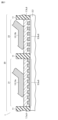
実施の形態1に係る半導体装置について説明する。図1および図2に示すように、半導体装置1では、半導体素子2が形成された半導体基板3(半導体デバイス)の一方の主面に、金属配線13がボンディングされるボンディング領域20が規定されている。金属配線13として、たとえば、銅配線(ワイヤ)が接続されている。
ここでは、第2構造体となる金属層77(図7参照)に、第2凹凸部8を意図的に形成する場合について説明する。たとえば、金属層77に、下地の形状が反映されない場合には、金属層77に第2凹凸部8を形成する必要がある。また、第1構造体5の第1凹凸部6とは異なるパターンを有する第2凹凸部8を金属層77に形成する場合がある。
上述した半導体装置1では、第1凹凸部6は、ドット状の凸部となる態様で形成され、第2凹凸部8は、そのドット状の第1凹凸部6を反映したドット状の凸部が形成されている場合を例に挙げて説明した。ここでは、第1凹凸部6および第2凹凸部8の、凸部または凹部のパターンのバリエーションについて説明する。
ここでは、第1構造体5と第2構造体7との間に中間構造体を介在させた半導体装置について説明する。中間構造体は、第1構造体5と第2構造体7との密着性の向上のために形成される。また、中間構造体は、第1構造体5と第2構造体7との間でそれぞれの材料の拡散を抑制するために形成される。
実施の形態1では、第1構造体5として、複数の凸部が互いに離間する態様で、半導体基板3の主面に配置されている場合について説明した。ここでは、連続した膜状の第1構造体5を備えた半導体装置の一例について説明する。
ここでは、ボンディング領域20における第1構造体5のバリエーションについて説明する。
図26に示すように、ボンディング領域20における第1領域21では、第1構造体5として、第1凹凸部6の複数の凸部が互いに離間する態様で半導体基板3の主面に配置された第1構造体5aが形成されている。一方、ボンディング領域20における第2領域23では、第1構造体5として、第1凹凸部6を有する連続した膜状の第1構造体5bが形成されている。
図27に示すように、ボンディング領域20における第1領域21では、第1構造体5として、第1凹凸部6を有する連続した膜状の第1構造体5aが形成されている。一方、ボンディング領域20における第2領域23では、第1構造体5として、第1凹凸部6の複数の凸部が互いに離間する態様で半導体基板3の主面に配置された第1構造体5bが形成されている。
ここでは、ボンディング領域20として、一つの領域からなるボンディング領域20を備えた半導体装置1について説明する。
図28に示すように、ボンディング領域20は一の領域25からなる。一の領域25は、絶縁性部材11によって規定されている。一の領域25では、第1構造体5として、第1凹凸部6を有する連続した膜状の第1構造体5が形成されている。その第1構造体5を覆うように、第2凹凸部8を有する第2構造体7が形成されている。
図29に示すように、ボンディング領域20は一の領域25からなる。一の領域25は、絶縁性部材11によって規定されている。一の領域25では、第1構造体5として、第1凹凸部6の複数の凸部が互いに離間する態様で半導体基板3の主面に配置された第1構造体5が形成されている。その第1構造体5を覆うように、第2凹凸部8を有する第2構造体7が形成されている。
ここでは、上述した実施の形態1~4において説明した半導体装置を適用した電力変換装置について説明する。本開示は特定の電力変換装置に限定されるものではないが、以下、実施の形態5として、三相のインバータに本開示を適用した場合について説明する。
Claims (16)
- 半導体素子が形成された半導体基板と、
前記半導体基板に規定されたボンディング領域と、
前記半導体基板に接するように形成され、前記ボンディング領域を規定する絶縁性部材と、
第1凹凸部を有し、前記ボンディング領域に形成された第1構造体と、
第2凹凸部を有し、前記第1構造体を覆うように形成された第2構造体と、
前記第2構造体における前記第2凹凸部に接合された金属配線とを有し、
前記第2凹凸部における凹みの深さは、前記第1凹凸部における凹みの深さよりも浅く、
前記絶縁性部材は、前記第1構造体および前記第2構造体を取り囲むように形成された、半導体装置。 - 半導体素子が形成された半導体基板と、
前記半導体基板に規定されたボンディング領域と、
第1凹凸部を有し、前記ボンディング領域に形成された第1構造体と、
前記第1構造体上に形成された中間構造体と、
第2凹凸部を有し、前記第1構造体及び前記中間構造体を覆うように形成された第2構造体と、
前記第2構造体における前記第2凹凸部に接合された金属配線とを有し、
前記第2凹凸部における凹みの深さは、前記第1凹凸部における凹みの深さよりも浅い、半導体装置。 - 前記第1構造体と前記第2構造体との間に、中間構造体を介在させた、請求項1に記載の半導体装置。
- 前記第1構造体は、凸部が互いに離間される態様で断続的に形成された前記第1凹凸部を含む、請求項1~3のいずれか1項に記載の半導体装置。
- 前記第1構造体は、連続する膜状に形成された前記第1凹凸部を含む、請求項1~3のいずれか1項に記載の半導体装置。
- 前記ボンディング領域は、
第1面積を有する第1領域と、
前記第1面積よりも小さい第2面積を有する第2領域とに区画された、請求項1~5のいずれか1項に記載の半導体装置。 - 前記第1構造体および前記第2構造体は、少なくとも前記第2領域に配置された、請求項6記載の半導体装置。
- 前記第2構造体は、ビッカース硬度が300以上の金属から形成された、請求項1~7のいずれか1項に記載の半導体装置。
- 前記金属は、ニッケル(Ni)、コバルト(Co)およびクロム(Cr)を含む、請求項8記載の半導体装置。
- 前記第1構造体は、酸化物を含む、請求項1~9のいずれか1項に記載の半導体装置。
- 前記金属配線は、銅配線を含む、請求項1~10のいずれか1項に記載の半導体装置。
- 半導体基板の主面に半導体素子を形成する工程と、
前記半導体基板の前記主面に、第1凹凸部を有する第1構造体を形成する工程と、
前記第1構造体を覆うように、第2凹凸部を有する第2構造体を形成する工程と、
前記第1構造体および前記第2構造体を少なくとも取り囲むように、絶縁性部材を形成することにより、ボンディング領域を規定する工程と、
前記ボンディング領域における前記第2構造体に、金属配線を接合する工程とを備え、
前記第1構造体を形成する工程および前記第2構造体を形成する工程では、前記第1構造体と前記第2構造体とは、前記第2凹凸部における凹みの深さが、前記第1凹凸部における凹みの深さよりも浅くなるように形成され、
前記ボンディング領域を規定する工程は、前記絶縁性部材を前記半導体基板の前記主面に達する態様で形成する工程を含む、
半導体装置の製造方法。 - 前記第1構造体を形成する工程は、前記半導体基板の前記主面上に第1層を形成し、前記第1層に、前記半導体基板の前記主面を部分的に露出する加工を施すことによって、凸部が離間された断続的な前記第1凹凸部を形成する工程を含む、請求項12記載の半導体装置の製造方法。
- 前記第1構造体を形成する工程は、前記半導体基板の前記主面上に第1層を形成し、前記第1層に、前記半導体基板の前記主面に至る途中まで加工を施すことによって、連続する膜状の前記第1凹凸部を形成する工程を含む、請求項12記載の半導体装置の製造方法。
- 前記金属配線を前記第2構造体に接合する工程は、前記金属配線として銅配線を接合する工程を含む、請求項12~14のいずれか1項に記載の半導体装置の製造方法。
- 請求項1~11のいずれか1項に記載の半導体装置を有し、入力される電力を変換して出力する主変換回路と、
前記主変換回路を制御する制御信号を前記主変換回路に出力する制御回路とを備えた、電力変換装置。
Applications Claiming Priority (1)
| Application Number | Priority Date | Filing Date | Title |
|---|---|---|---|
| PCT/JP2020/021175 WO2021240748A1 (ja) | 2020-05-28 | 2020-05-28 | 半導体装置およびその製造方法ならびに電力変換装置 |
Publications (3)
| Publication Number | Publication Date |
|---|---|
| JPWO2021240748A1 JPWO2021240748A1 (ja) | 2021-12-02 |
| JPWO2021240748A5 JPWO2021240748A5 (ja) | 2022-11-17 |
| JP7391210B2 true JP7391210B2 (ja) | 2023-12-04 |
Family
ID=78723199
Family Applications (1)
| Application Number | Title | Priority Date | Filing Date |
|---|---|---|---|
| JP2022527416A Active JP7391210B2 (ja) | 2020-05-28 | 2020-05-28 | 半導体装置およびその製造方法ならびに電力変換装置 |
Country Status (5)
| Country | Link |
|---|---|
| US (1) | US20230197649A1 (ja) |
| JP (1) | JP7391210B2 (ja) |
| CN (1) | CN115699267A (ja) |
| DE (1) | DE112020007244T5 (ja) |
| WO (1) | WO2021240748A1 (ja) |
Citations (6)
| Publication number | Priority date | Publication date | Assignee | Title |
|---|---|---|---|---|
| JP4348047B2 (ja) | 2002-04-15 | 2009-10-21 | 花王株式会社 | 変異アルカリプロテアーゼ |
| JP2013080809A (ja) | 2011-10-04 | 2013-05-02 | Panasonic Corp | 半導体装置 |
| JP2014027048A (ja) | 2012-07-25 | 2014-02-06 | Renesas Electronics Corp | 半導体ウェハ及び半導体装置の製造方法 |
| JP6310551B2 (ja) | 2013-06-13 | 2018-04-11 | コーニンクレッカ フィリップス エヌ ヴェKoninklijke Philips N.V. | 放射線療法治療の案内および検証のための検出器 |
| JP6364035B2 (ja) | 2016-01-29 | 2018-07-25 | 京セラ株式会社 | 携帯電話、表示制御方法、およびプログラム |
| JP2020043154A (ja) | 2018-09-07 | 2020-03-19 | 三菱電機株式会社 | 半導体装置及びその製造方法、並びに、電力変換装置 |
Family Cites Families (6)
| Publication number | Priority date | Publication date | Assignee | Title |
|---|---|---|---|---|
| JPS6310551U (ja) * | 1986-07-09 | 1988-01-23 | ||
| JPS6364035U (ja) * | 1986-10-16 | 1988-04-27 | ||
| JPH0225045A (ja) | 1988-07-13 | 1990-01-26 | Oki Electric Ind Co Ltd | 半導体装置 |
| JPH04348047A (ja) * | 1991-05-24 | 1992-12-03 | Mitsubishi Electric Corp | 半導体集積回路電極 |
| JPH0543544U (ja) * | 1991-11-12 | 1993-06-11 | 日本無線株式会社 | 電子素子の接続端子構造 |
| JP6068425B2 (ja) | 2014-12-11 | 2017-01-25 | 株式会社神戸製鋼所 | 電極構造 |
-
2020
- 2020-05-28 WO PCT/JP2020/021175 patent/WO2021240748A1/ja active Application Filing
- 2020-05-28 DE DE112020007244.4T patent/DE112020007244T5/de active Pending
- 2020-05-28 JP JP2022527416A patent/JP7391210B2/ja active Active
- 2020-05-28 CN CN202080101224.5A patent/CN115699267A/zh active Pending
- 2020-05-28 US US17/913,442 patent/US20230197649A1/en active Pending
Patent Citations (6)
| Publication number | Priority date | Publication date | Assignee | Title |
|---|---|---|---|---|
| JP4348047B2 (ja) | 2002-04-15 | 2009-10-21 | 花王株式会社 | 変異アルカリプロテアーゼ |
| JP2013080809A (ja) | 2011-10-04 | 2013-05-02 | Panasonic Corp | 半導体装置 |
| JP2014027048A (ja) | 2012-07-25 | 2014-02-06 | Renesas Electronics Corp | 半導体ウェハ及び半導体装置の製造方法 |
| JP6310551B2 (ja) | 2013-06-13 | 2018-04-11 | コーニンクレッカ フィリップス エヌ ヴェKoninklijke Philips N.V. | 放射線療法治療の案内および検証のための検出器 |
| JP6364035B2 (ja) | 2016-01-29 | 2018-07-25 | 京セラ株式会社 | 携帯電話、表示制御方法、およびプログラム |
| JP2020043154A (ja) | 2018-09-07 | 2020-03-19 | 三菱電機株式会社 | 半導体装置及びその製造方法、並びに、電力変換装置 |
Also Published As
| Publication number | Publication date |
|---|---|
| DE112020007244T5 (de) | 2023-03-09 |
| WO2021240748A1 (ja) | 2021-12-02 |
| CN115699267A (zh) | 2023-02-03 |
| US20230197649A1 (en) | 2023-06-22 |
| JPWO2021240748A1 (ja) | 2021-12-02 |
Similar Documents
| Publication | Publication Date | Title |
|---|---|---|
| JP6972432B1 (ja) | 半導体パッケージ、半導体装置および電力変換装置 | |
| JP2018190930A (ja) | パワー半導体モジュール及びその製造方法並びに電力変換装置 | |
| JP6826665B2 (ja) | 半導体装置、半導体装置の製造方法及び電力変換装置 | |
| JP2019102535A (ja) | 半導体モジュール、その製造方法及び電力変換装置 | |
| JP6987031B2 (ja) | 電力用半導体装置及びその製造方法、並びに、電力変換装置 | |
| JP7391210B2 (ja) | 半導体装置およびその製造方法ならびに電力変換装置 | |
| JP6892023B1 (ja) | 半導体装置、半導体装置の製造方法および電力変換装置 | |
| JP6927437B1 (ja) | パワーモジュールおよび電力変換装置 | |
| JP2014053403A (ja) | パワーモジュール半導体装置 | |
| WO2022186192A1 (ja) | 半導体素子、電力変換装置および半導体素子の製造方法 | |
| US10083889B2 (en) | Electronic component package including sealing resin layer, metal member, ceramic substrate, and electronic component and method for manufacturing the same | |
| JP6410998B1 (ja) | 半導体モジュール、半導体モジュールの製造方法および電力変換装置 | |
| JP2021061332A (ja) | 半導体装置および電力変換装置 | |
| JP7088421B1 (ja) | 半導体装置および電力変換装置 | |
| JP7438466B1 (ja) | 半導体装置及びその製造方法並びに電力変換装置 | |
| WO2023190839A1 (ja) | 半導体装置 | |
| WO2022049997A1 (ja) | 素子パッケージおよび半導体装置 | |
| JP7101885B2 (ja) | パワー半導体モジュール及び電力変換装置 | |
| JP6885522B1 (ja) | 半導体装置、電力変換装置および半導体装置の製造方法 | |
| US20240087978A1 (en) | Semiconductor device | |
| WO2023175854A1 (ja) | 半導体装置、電力変換装置および半導体装置の製造方法 | |
| JP6906681B2 (ja) | 半導体素子、半導体装置、電力変換装置、及び、半導体素子の製造方法 | |
| WO2022249951A1 (ja) | パワー半導体装置及び電力変換装置 | |
| WO2021002006A1 (ja) | 半導体装置、電力変換装置および半導体装置の製造方法 | |
| JP2022007599A (ja) | 半導体装置 |
Legal Events
| Date | Code | Title | Description |
|---|---|---|---|
| A521 | Request for written amendment filed |
Free format text: JAPANESE INTERMEDIATE CODE: A523 Effective date: 20220915 |
|
| A621 | Written request for application examination |
Free format text: JAPANESE INTERMEDIATE CODE: A621 Effective date: 20220915 |
|
| TRDD | Decision of grant or rejection written | ||
| A01 | Written decision to grant a patent or to grant a registration (utility model) |
Free format text: JAPANESE INTERMEDIATE CODE: A01 Effective date: 20231024 |
|
| A61 | First payment of annual fees (during grant procedure) |
Free format text: JAPANESE INTERMEDIATE CODE: A61 Effective date: 20231121 |
|
| R150 | Certificate of patent or registration of utility model |
Ref document number: 7391210 Country of ref document: JP Free format text: JAPANESE INTERMEDIATE CODE: R150 |