WO2021220738A1 - 液晶表示装置 - Google Patents
液晶表示装置 Download PDFInfo
- Publication number
- WO2021220738A1 WO2021220738A1 PCT/JP2021/014663 JP2021014663W WO2021220738A1 WO 2021220738 A1 WO2021220738 A1 WO 2021220738A1 JP 2021014663 W JP2021014663 W JP 2021014663W WO 2021220738 A1 WO2021220738 A1 WO 2021220738A1
- Authority
- WO
- WIPO (PCT)
- Prior art keywords
- liquid crystal
- crystal display
- display device
- light
- polarizing element
- Prior art date
- Legal status (The legal status is an assumption and is not a legal conclusion. Google has not performed a legal analysis and makes no representation as to the accuracy of the status listed.)
- Ceased
Links
Images




Classifications
-
- G—PHYSICS
- G02—OPTICS
- G02F—OPTICAL DEVICES OR ARRANGEMENTS FOR THE CONTROL OF LIGHT BY MODIFICATION OF THE OPTICAL PROPERTIES OF THE MEDIA OF THE ELEMENTS INVOLVED THEREIN; NON-LINEAR OPTICS; FREQUENCY-CHANGING OF LIGHT; OPTICAL LOGIC ELEMENTS; OPTICAL ANALOGUE/DIGITAL CONVERTERS
- G02F1/00—Devices or arrangements for the control of the intensity, colour, phase, polarisation or direction of light arriving from an independent light source, e.g. switching, gating or modulating; Non-linear optics
- G02F1/01—Devices or arrangements for the control of the intensity, colour, phase, polarisation or direction of light arriving from an independent light source, e.g. switching, gating or modulating; Non-linear optics for the control of the intensity, phase, polarisation or colour
- G02F1/13—Devices or arrangements for the control of the intensity, colour, phase, polarisation or direction of light arriving from an independent light source, e.g. switching, gating or modulating; Non-linear optics for the control of the intensity, phase, polarisation or colour based on liquid crystals, e.g. single liquid crystal display cells
- G02F1/133—Constructional arrangements; Operation of liquid crystal cells; Circuit arrangements
- G02F1/1333—Constructional arrangements; Manufacturing methods
- G02F1/1335—Structural association of cells with optical devices, e.g. polarisers or reflectors
- G02F1/1336—Illuminating devices
- G02F1/13362—Illuminating devices providing polarized light, e.g. by converting a polarisation component into another one
-
- G—PHYSICS
- G02—OPTICS
- G02F—OPTICAL DEVICES OR ARRANGEMENTS FOR THE CONTROL OF LIGHT BY MODIFICATION OF THE OPTICAL PROPERTIES OF THE MEDIA OF THE ELEMENTS INVOLVED THEREIN; NON-LINEAR OPTICS; FREQUENCY-CHANGING OF LIGHT; OPTICAL LOGIC ELEMENTS; OPTICAL ANALOGUE/DIGITAL CONVERTERS
- G02F1/00—Devices or arrangements for the control of the intensity, colour, phase, polarisation or direction of light arriving from an independent light source, e.g. switching, gating or modulating; Non-linear optics
- G02F1/01—Devices or arrangements for the control of the intensity, colour, phase, polarisation or direction of light arriving from an independent light source, e.g. switching, gating or modulating; Non-linear optics for the control of the intensity, phase, polarisation or colour
- G02F1/13—Devices or arrangements for the control of the intensity, colour, phase, polarisation or direction of light arriving from an independent light source, e.g. switching, gating or modulating; Non-linear optics for the control of the intensity, phase, polarisation or colour based on liquid crystals, e.g. single liquid crystal display cells
- G02F1/133—Constructional arrangements; Operation of liquid crystal cells; Circuit arrangements
- G02F1/1333—Constructional arrangements; Manufacturing methods
- G02F1/133302—Rigid substrates, e.g. inorganic substrates
-
- G—PHYSICS
- G02—OPTICS
- G02F—OPTICAL DEVICES OR ARRANGEMENTS FOR THE CONTROL OF LIGHT BY MODIFICATION OF THE OPTICAL PROPERTIES OF THE MEDIA OF THE ELEMENTS INVOLVED THEREIN; NON-LINEAR OPTICS; FREQUENCY-CHANGING OF LIGHT; OPTICAL LOGIC ELEMENTS; OPTICAL ANALOGUE/DIGITAL CONVERTERS
- G02F1/00—Devices or arrangements for the control of the intensity, colour, phase, polarisation or direction of light arriving from an independent light source, e.g. switching, gating or modulating; Non-linear optics
- G02F1/01—Devices or arrangements for the control of the intensity, colour, phase, polarisation or direction of light arriving from an independent light source, e.g. switching, gating or modulating; Non-linear optics for the control of the intensity, phase, polarisation or colour
- G02F1/13—Devices or arrangements for the control of the intensity, colour, phase, polarisation or direction of light arriving from an independent light source, e.g. switching, gating or modulating; Non-linear optics for the control of the intensity, phase, polarisation or colour based on liquid crystals, e.g. single liquid crystal display cells
- G02F1/133—Constructional arrangements; Operation of liquid crystal cells; Circuit arrangements
- G02F1/1333—Constructional arrangements; Manufacturing methods
- G02F1/1335—Structural association of cells with optical devices, e.g. polarisers or reflectors
- G02F1/133528—Polarisers
-
- G—PHYSICS
- G02—OPTICS
- G02F—OPTICAL DEVICES OR ARRANGEMENTS FOR THE CONTROL OF LIGHT BY MODIFICATION OF THE OPTICAL PROPERTIES OF THE MEDIA OF THE ELEMENTS INVOLVED THEREIN; NON-LINEAR OPTICS; FREQUENCY-CHANGING OF LIGHT; OPTICAL LOGIC ELEMENTS; OPTICAL ANALOGUE/DIGITAL CONVERTERS
- G02F1/00—Devices or arrangements for the control of the intensity, colour, phase, polarisation or direction of light arriving from an independent light source, e.g. switching, gating or modulating; Non-linear optics
- G02F1/01—Devices or arrangements for the control of the intensity, colour, phase, polarisation or direction of light arriving from an independent light source, e.g. switching, gating or modulating; Non-linear optics for the control of the intensity, phase, polarisation or colour
- G02F1/13—Devices or arrangements for the control of the intensity, colour, phase, polarisation or direction of light arriving from an independent light source, e.g. switching, gating or modulating; Non-linear optics for the control of the intensity, phase, polarisation or colour based on liquid crystals, e.g. single liquid crystal display cells
- G02F1/133—Constructional arrangements; Operation of liquid crystal cells; Circuit arrangements
- G02F1/1333—Constructional arrangements; Manufacturing methods
- G02F1/1335—Structural association of cells with optical devices, e.g. polarisers or reflectors
- G02F1/133528—Polarisers
- G02F1/133536—Reflective polarizers
-
- G—PHYSICS
- G02—OPTICS
- G02F—OPTICAL DEVICES OR ARRANGEMENTS FOR THE CONTROL OF LIGHT BY MODIFICATION OF THE OPTICAL PROPERTIES OF THE MEDIA OF THE ELEMENTS INVOLVED THEREIN; NON-LINEAR OPTICS; FREQUENCY-CHANGING OF LIGHT; OPTICAL LOGIC ELEMENTS; OPTICAL ANALOGUE/DIGITAL CONVERTERS
- G02F1/00—Devices or arrangements for the control of the intensity, colour, phase, polarisation or direction of light arriving from an independent light source, e.g. switching, gating or modulating; Non-linear optics
- G02F1/01—Devices or arrangements for the control of the intensity, colour, phase, polarisation or direction of light arriving from an independent light source, e.g. switching, gating or modulating; Non-linear optics for the control of the intensity, phase, polarisation or colour
- G02F1/13—Devices or arrangements for the control of the intensity, colour, phase, polarisation or direction of light arriving from an independent light source, e.g. switching, gating or modulating; Non-linear optics for the control of the intensity, phase, polarisation or colour based on liquid crystals, e.g. single liquid crystal display cells
- G02F1/133—Constructional arrangements; Operation of liquid crystal cells; Circuit arrangements
- G02F1/1333—Constructional arrangements; Manufacturing methods
- G02F1/1335—Structural association of cells with optical devices, e.g. polarisers or reflectors
- G02F1/133528—Polarisers
- G02F1/133548—Wire-grid polarisers
-
- G—PHYSICS
- G02—OPTICS
- G02F—OPTICAL DEVICES OR ARRANGEMENTS FOR THE CONTROL OF LIGHT BY MODIFICATION OF THE OPTICAL PROPERTIES OF THE MEDIA OF THE ELEMENTS INVOLVED THEREIN; NON-LINEAR OPTICS; FREQUENCY-CHANGING OF LIGHT; OPTICAL LOGIC ELEMENTS; OPTICAL ANALOGUE/DIGITAL CONVERTERS
- G02F1/00—Devices or arrangements for the control of the intensity, colour, phase, polarisation or direction of light arriving from an independent light source, e.g. switching, gating or modulating; Non-linear optics
- G02F1/01—Devices or arrangements for the control of the intensity, colour, phase, polarisation or direction of light arriving from an independent light source, e.g. switching, gating or modulating; Non-linear optics for the control of the intensity, phase, polarisation or colour
- G02F1/13—Devices or arrangements for the control of the intensity, colour, phase, polarisation or direction of light arriving from an independent light source, e.g. switching, gating or modulating; Non-linear optics for the control of the intensity, phase, polarisation or colour based on liquid crystals, e.g. single liquid crystal display cells
- G02F1/133—Constructional arrangements; Operation of liquid crystal cells; Circuit arrangements
- G02F1/1333—Constructional arrangements; Manufacturing methods
- G02F1/1335—Structural association of cells with optical devices, e.g. polarisers or reflectors
- G02F1/1336—Illuminating devices
- G02F1/133602—Direct backlight
- G02F1/133606—Direct backlight including a specially adapted diffusing, scattering or light controlling members
-
- G—PHYSICS
- G02—OPTICS
- G02F—OPTICAL DEVICES OR ARRANGEMENTS FOR THE CONTROL OF LIGHT BY MODIFICATION OF THE OPTICAL PROPERTIES OF THE MEDIA OF THE ELEMENTS INVOLVED THEREIN; NON-LINEAR OPTICS; FREQUENCY-CHANGING OF LIGHT; OPTICAL LOGIC ELEMENTS; OPTICAL ANALOGUE/DIGITAL CONVERTERS
- G02F2202/00—Materials and properties
- G02F2202/28—Adhesive materials or arrangements
-
- G—PHYSICS
- G02—OPTICS
- G02F—OPTICAL DEVICES OR ARRANGEMENTS FOR THE CONTROL OF LIGHT BY MODIFICATION OF THE OPTICAL PROPERTIES OF THE MEDIA OF THE ELEMENTS INVOLVED THEREIN; NON-LINEAR OPTICS; FREQUENCY-CHANGING OF LIGHT; OPTICAL LOGIC ELEMENTS; OPTICAL ANALOGUE/DIGITAL CONVERTERS
- G02F2203/00—Function characteristic
- G02F2203/01—Function characteristic transmissive
Definitions
- the present disclosure relates to a liquid crystal display device that can be used for projection display of image light and the like.
- Patent Document 1 An example of the prior art is described in, for example, Patent Document 1.
- the liquid crystal display device of the present disclosure includes a light-transmitting liquid crystal display element having two transparent substrates and a liquid crystal layer sealed between the two transparent substrates.
- An incident-side polarizing plate located on one of the transparent substrates of the liquid crystal display element, A light source that emits light toward the transparent substrate on one of the liquid crystal display elements, A plate-shaped polarizing element having a base layer formed of glass and a metal layer having a polarizing function laminated on the base layer is provided.
- the polarizing element is arranged between the light source and the liquid crystal display element so that the metal layer faces the light source.
- the thickness of the base layer is thicker than the thickness of each of the two transparent substrates.
- the liquid crystal display device of the present disclosure it is possible to prevent light omission of the black display of the projected image and display a high-quality image without impairing the sense of reality as the temperature of the light source, which is also called a backlight, increases.
- the metal layer constituting the polarizing element also functions as a good heat conduction member and a good heat diffusion member that receives the light radiated from the backlight, receives the radiant heat, and transfers and diffuses the heat to the surroundings.
- the base layer constituting the polarizing element is thicker than the thickness of each of the two transparent substrates, the heat capacity is increased.
- FIG. 5 is a partially enlarged cross-sectional view showing an enlarged side surface portion of a polarizing element with respect to the liquid crystal display device of another example of the embodiment of the present disclosure.
- FIG. 5 is a partially enlarged cross-sectional view showing an enlarged side surface portion of a polarizing element with respect to the liquid crystal display device of another example of the embodiment of the present disclosure.
- Patent Document 1 describes that the brightness of the backlight is reduced by a predetermined frequency.
- FIG. 1 is a cross-sectional view schematically showing the configuration of a liquid crystal display device 1 of an example of the embodiment of the present disclosure. It should be noted that FIG. 1 is shown in a state of being disassembled in the thickness direction for easy illustration.
- the liquid crystal display device 1 of the present embodiment is a light transmissive type having a glass substrates 2a and 2b as two transparent substrates and a liquid crystal layer 3 sealed between the two glass substrates 2a and 2b.
- a liquid crystal display element 4, a backlight device 5 as a light source that emits light toward one glass substrate 2a of the liquid crystal display element 4, and an emitting side polarizing plate located on the other glass substrate 2b of the liquid crystal display element 4.
- an incident side polarizing plate 7 located on one of the glass substrates 2a of the liquid crystal display element 4, a base layer 8 formed of glass, and a metal layer 9 having a polarizing function laminated on the base layer 8.
- the plate-shaped polarizing element 10 is provided.
- the polarizing element 10 is arranged between the backlight device 5 and the liquid crystal display element 4 so that the metal layer 9 faces the backlight device 5, and the thickness of the base layer 8 is two glass substrates.
- the configuration is thicker than the respective thicknesses of 2a and 2b.
- the above configuration has the following effects.
- the metal layer 9 constituting the polarizing element 10 also functions as a good heat conduction member and a good heat diffusion member that receives the light radiated from the backlight device 5 and receives the radiant heat to transfer and diffuse the heat to the surroundings. .. Further, since the base layer 8 constituting the polarizing element 10 has an increased heat capacity, it receives the light radiated from the backlight device 5 and receives the radiant heat, and the radiant heat transmitted to the liquid crystal display element 4 side is effective. It also functions as a heat insulating member that reduces the amount of heat.
- the transparent substrate constituting the liquid crystal display element 4 may be a glass substrate, a transparent resin substrate, a translucent ceramic substrate, or the like. Further, the transparent substrate may be a composite type substrate in which a plurality of types of substrates such as a glass substrate, a transparent resin substrate, and a translucent ceramic substrate are laminated.
- the transparent substrate is a composite substrate in which a glass substrate and a transparent resin substrate are laminated, the glass has a thermal conductivity of 0.55 to 0.75 (W / mK) and the resin material is 0.12 to 0.12 to Since it is higher than 0.29 (W / mK), the glass substrate may be arranged so as to be located on the side of the backlight device 5 and the metal layer 9.
- the metal layer 9 which also functions as a good heat conductive member and a good heat diffusion member, and a glass substrate in contact with the metal layer 9.
- the glass substrate is suitable because it is easy to process, inexpensive, and has a high transmittance.
- the base layer 8 constituting the polarizing element 10 has an increased heat capacity, the thermal influence on the liquid crystal display element 4 can be reduced, and as a result, the two glass substrates 2a constituting the liquid crystal display element 4 can be reduced. , 2b can also be made thinner.
- the polarizing element 10 is arranged so that the metal layer 9 faces the backlight device 5.
- the metal layer 9 which is also a good heat conductive member and a good heat diffusion member, can effectively receive the light radiated from the backlight device 5 and effectively receive the radiant heat.
- the thickness T3 of the base layer 8 is thicker than the thicknesses T1 and T2 of the two glass substrates 2a and 2b, respectively.
- the heat capacity of the base layer 8 which is also a heat insulating member is increased, and the light radiated from the backlight device 5 can be received to effectively store and insulate the radiant heat.
- the heat insulation does not mean a complete blockage of heat transfer, but means a heat insulation effect to the extent that the purpose of preventing light leakage of the black display in the liquid crystal display element 4 can be achieved.
- the thicknesses T1 and T2 of the glass substrates 2a and 2b are, for example, about 200 ⁇ m to 1000 ⁇ m.
- the thicknesses T1 and T2 of these glass substrates 2a and 2b may be the same or different.
- the thickness T3 of the base layer 8 is more than 1 times and about 5 times or less of the thickness of one of the thicknesses T1 and T2, whichever is thicker, or when the thicknesses T1 and T2 are the same, preferably about. It is selected as 2 times or more and about 5 times or less. If it exceeds 5 times, the device tends to be large and heavy.
- "-" means "to", and the same applies hereinafter.
- the thickness T3 of the base layer 8 may be thicker than the total thickness (T1 + T2) of the respective thicknesses T1 and T2 of the two glass substrates 2a and 2b.
- the heat capacity of the base layer 8 which is also a heat insulating member is further increased, and the light radiated from the backlight device 5 can be received to more effectively store and insulate the radiant heat.
- the mechanical strength of the liquid crystal display element 4 is remarkably improved.
- the thickness T1 of the glass substrate 2a on the side closer to the backlight 5 is the thickness of the glass substrate 2b on the side farther from the backlight 5.
- the configuration may be thicker than T2.
- the glass substrate 2a since the heat capacity of the glass substrate 2a increases, the glass substrate 2a receives the light radiated from the backlight device 5, receives the radiant heat, and effectively reduces the radiant heat transmitted to the liquid crystal display. It also functions as a member.
- T1 may be more than 1 times and less than 2 times that of T2, but is not limited to this range.
- the base layer 8 is formed of glass, but the polarizing element 10 may be, for example, a glass substrate.
- the glass since the glass has translucency, the light of the backlight device 5 can be appropriately transmitted to the side of the liquid crystal display element 4.
- the glass is silicon oxide (SiO 2 ), aluminum oxide (Al 2 O 3 ), boric acid (B 2 O 3 ), sodium oxide (Na 2 O), potassium oxide (K 2 O), calcium oxide (CaO). Since it contains various chemically stable oxides such as, there is almost no deterioration due to heat, and heat can be effectively stored and heat-insulated for a long period of time.
- the thermal conductivity of glass is 0.55 to 0.75 (W / mK), which is higher than that of the resin material of 0.12 to 0.29 (W / mK), the glass is compared with the resin material.
- the thermal effect on the liquid crystal display element 4 is smaller than that of the resin material, and the heat distribution tends to be uniform as a whole.
- the base layer 8 of the polarizing element 10 is a glass substrate, even if it is composed of blue plate glass (soda glass) containing silicon oxide (SiO 2 ), sodium oxide (Na 2 O), and calcium oxide (CaO) as main components. good. Blue plate glass has the lowest melting point among glass, is easy to process, and is inexpensive.
- the base layer 8 is a glass substrate, it is composed of white plate glass (non-alikari glass) containing silicon oxide (SiO 2 ), boric acid (B 2 O 3 ), and aluminum oxide (Al 2 O 3) as main components. May be.
- White plate glass is inexpensive, has high transmittance in the wavelength range of visible light, ultraviolet light, and infrared light, and the upper limit of general normal use temperature is 120 ° C to 130 ° C, which is equivalent to that of blue plate glass.
- the base layer 8 When the base layer 8 is a glass substrate, it may be made of quartz glass containing silicon oxide (SiO 2) as a main component. Quartz glass is a high-purity glass with few impurities, has a high transmittance for ultraviolet light and infrared light, and has a high heat resistant temperature. The upper limit of the normal operating temperature of quartz glass is about 900 ° C. In addition, quartz glass has excellent chemical resistance and is easy to perform such as drilling and cutting.
- the base layer 8 of the polarizing element 10 may be a sapphire glass (Al 2 O 3 single crystal) substrate (also referred to as a sapphire crystal substrate).
- Sapphire glass has a high Mohs hardness of 9, a heat resistant temperature of about 2000 ° C., a thermal conductivity of 42 W / mK (20 ° C.), and a number of glass thermal conductivity of 1.4 W / mK (20 ° C.). It is 10 times.
- the polarizing element 10 may be arranged at a distance from the backlight device 5. In this case, since the polarizing element 10 is not in contact with the backlight device 5, the polarizing element 10 does not directly receive the heat of the backlight device 5 itself by heat conduction. As a result, it is possible to prevent the polarizing element 10 from becoming abnormally high in temperature.
- the interval g1 may be, for example, about 0.1 mm to 10 mm.
- the interval g1 is not limited to this range.
- the air layers existing at the interval g1 are likely to be convected, and heat transfer due to convection is likely to occur.
- the interval g1 exceeds, for example, 10 mm, the liquid crystal display device 1 tends to become large.
- the interval g1 when the interval g1 is less than 0.1 mm, for example, the volume of the air layer existing in the interval g1 is small, so that the heat insulating effect of the air layer is small and the polarizing element 10 radiates the heat of the backlight device 5 itself. It tends to be easier to receive heat. Further, the interval g1 may be about 1 mm to 5 mm.
- the polarizing element 10 may be arranged at a distance from the liquid crystal display element 4. In this case, since the polarizing element 10 is not in contact with the liquid crystal display element 4, the liquid crystal display element 4 does not directly receive the heat of the polarizing element 10 itself by heat conduction. As a result, it is possible to prevent the liquid crystal display element 4 from becoming abnormally high in temperature.
- the interval g2 may be, for example, about 0.1 mm to 10 mm.
- the interval g2 is not limited to this range. In this case, since the volume of the air layer existing at the interval g2 is large, the heat insulating effect of the air layer is increased, and the air layer existing at the interval g2 is easily convected, so that heat transfer due to convection is likely to occur.
- the interval g2 exceeds, for example, 10 mm, the liquid crystal display device 1 tends to become large.
- the interval g2 when the interval g2 is less than 0.1 mm, for example, the volume of the air layer existing in the interval g2 is small, so that the heat insulating effect of the air layer tends to be small. Further, the interval g2 may be about 1 mm to 5 mm.
- a light diffusing member 11 having light diffusing property may be interposed between the backlight device 5 and the incident side polarizing plate 7.
- the light diffusing member 11 homogenizes the light radiated from the backlight device 5 and emits it to the liquid crystal display element 4.
- the light diffusing member 11 has a plate-like shape made of a translucent resin such as a styrene / methyl methacrylate copolymer resin (MS resin), a polystyrene resin (PS resin), a polycarbonate resin (PC resin), and a cycloolefin resin (COP resin). It is composed of a base material mixed with a granular light diffusing agent made of acrylic resin, silicone resin, or the like.
- a light diffusing member 11 containing 85% by weight of MS resin, 10% by weight of PC resin, 2% by weight of COP resin, and 3% by weight of a light diffusing agent made of acrylic resin.
- the light diffusing member 11 also functions as a heat equalizing member that receives the light radiated from the backlight device 5 and uniformly receives the radiant heat as a whole. This is due to homogenizing the light emitted from the backlight device 5. Further, the light diffusing member 11 also has an effect of receiving the light radiated from the backlight device 5, storing the radiant heat, and insulating the heat. That is, it is considered that the light emitted from the backlight device 5 is repeatedly scattered in the light diffusing member 11, and thus the average optical path length in the light diffusing member 11 is increased.
- the light diffusing member 11 may be arranged between the backlight device 5 and the polarizing element 10.
- the base layer 8 of the polarizing element 10 made of a glass substrate or the like having a higher thermal conductivity and a larger heat capacity than the resin material is closer to the liquid crystal display element 4 than the light diffusing member 11 whose base material is made of the resin material. Therefore, the thermal influence on the liquid crystal display element 4 can be made smaller, and the heat distribution tends to be uniform as a whole. As a result, the heat distribution of the liquid crystal display element 4 can be easily made uniform.
- the light diffusing member 11 may be arranged between the backlight device 5 and the polarizing element 10 at a distance from the polarizing element 10. In this case, since the light diffusing member 11 is not in contact with the polarizing element 10, the polarizing element 10 does not directly receive the heat of the light diffusing member 11 itself by heat conduction. As a result, it is possible to prevent the polarizing element 10 from becoming abnormally high in temperature.
- the interval g3 may be about 0.1 mm to 10 mm.
- the interval g3 is not limited to this range. In this case, since the volume of the air layer existing at the interval g3 is large, the heat insulating effect of the air layer is increased, and the air layer existing at the interval g3 is easily convected, so that heat transfer due to convection is likely to occur.
- the interval g3 exceeds, for example, 10 mm, the liquid crystal display device 1 tends to become large.
- the interval g3 when the interval g3 is less than 0.1 mm, for example, the volume of the air layer existing in the interval g3 is small, so that the heat insulating effect of the air layer tends to be small. Further, the interval g3 may be about 1 mm to 5 mm.
- the light diffusing member 11 may be arranged between the backlight device 5 and the polarizing element 10 in contact with the polarizing element 10. In this case, the light diffusing member 11 and the polarizing element 10 are integrated to form a composite heat insulating member having a large heat capacity. Further, the light diffusing member 11 may be in contact with the polarizing element 10 via a translucent sheet, a translucent film, a translucent resin adhesive, or the like. In this case, the light diffusing member 11 and the polarizing element 10 are integrated to form a composite heat insulating member having a larger heat capacity.
- the polarization axis of the metal layer 9 is parallel to the polarization axis of the incident side polarizing plate 7.
- a conductive tape 12 is attached to the peripheral region of the metal layer 9 in order to enhance heat dissipation.
- the metal layer 9 includes a plurality of thin metal wires (also referred to as wire grids) 13 arranged in parallel with each other at intervals.
- FIG. 2 is a conceptual diagram for explaining the polarization function of the polarizing element 10.
- the polarizing element 10 has a base layer 8 and a metal layer 9.
- the surface portion of the base layer 8 on the backlight device 5 side has concave portions and convex portions alternately repeated along one direction X on one plane, and extends in another direction Y perpendicular to one direction X on one plane. It has an uneven pattern, and one or a plurality of the above-mentioned thin metal wires 13 may be joined to each concave portion. That is, the metal layer 9 may be a thin metal wire 13.
- the thin metal wire 13 may contain at least one of Al, Ag, Cu, Ni and Cr. That is, the thin metal wire 13 is one of Al, Ag, Cu, Ni, Cr, etc. (preferably a non-magnetic metal), a composition containing these as a main component, Al, Ag, Cu, Cr, etc.
- fine metal wires having a diameter or thickness of about 100 nm to about 500 nm, for example, a diameter or thickness of about 250 nm are arranged on one plane with a pitch of about 100 nm to about 200 nm.
- the configuration may be arranged in parallel at a pitch of about 130 nm.
- the thin metal wire 13 may be an Al alloy containing Al as a main component, and the Al alloy may be duralmin (Al—Cu alloy, Al—Cu—Mg alloy, Al—Zn—Mg—Cu alloy). ..
- the thin metal wire 13 may be an Ag alloy (Ag—Cu alloy) containing Ag as a main component.
- the thin metal wire 13 may be a Cu alloy containing Cu as a main component (Cu—Zn alloy, Cu—Zn—Ni alloy, Cu—Sn alloy, Cu—Sn—Zn alloy).
- the thin metal wire 13 may be an alloy containing Ni and Cr (Ni—Cr alloy, Ni—Cr—Fe alloy, Ni—Cr—Mo alloy).
- the thin metal wire 13 is an Fe alloy containing Fe as a main component (Fe—Ni alloy, Fe—Ni36% alloy (Inver), Fe—Ni—Co alloy (Cobal), Fe—Cr alloy, Fe—Cr—Ni alloy). It may be.
- the thin metal wire 13 may be made of a non-magnetic metal.
- the thin metal wire 13 is made of a magnetic metal that is easily magnetized by an external magnetic field such as a ferromagnetic material
- the linear polarization is polarized together with the strength of the magnetic field by the magnetic field generated by the thin metal wire 13.
- the surface rotates. That is, the Faraday effect, which is a kind of magneto-optical effect, occurs.
- the plane of linearly polarized light passing through the polarizing element 10 rotates, inconsistency with the cross Nicol condition of the liquid crystal display element 4 occurs. As a result, the liquid crystal display element 4 tends to deteriorate in display quality such as a decrease in contrast.
- the thin metal wire 13 may be made of a paramagnetic metal as a non-magnetic metal.
- the paramagnetic metal include aluminum (Al), chromium (Cr), molybdenum (Mo), titanium (Ti), zirconium (Zr) and the like.
- the thin metal wire 13 may be composed of a diamagnetic metal as a non-magnetic metal. Examples of the diamagnetic metal include gold (Au), silver (Ag), copper (Cu), zinc (Zn) and the like.
- the thin metal wire 13 may be made of non-magnetic stainless steel that is not easily magnetized by an external magnetic field.
- the thin metal wire 13 may be made of completely non-magnetic brass (Cu—Zn alloy) or the like that is not magnetized by an external magnetic field.
- the thin metal wire 13 may have a laminated structure in which a plurality of layers of the above-mentioned various metal layers, various alloy layers, and various non-magnetic metal layers are laminated.
- a Mo layer, a Ti layer, or the like having a high hardness may be laminated on the lower layer side and / or the upper layer side of the Al layer having a high thermal conductivity but a low hardness.
- the inventor of the present application has investigated that there are the following reasons for light leakage. That is, the cause of light leakage is birefringence caused by the photoelastic effect of glass due to the shrinkage of the polarizing plate due to the in-plane distribution of the polarizing plate surface temperature on the light source side, and the driving method of the liquid crystal display element 4 is peculiar to the IPS mode. I found out that there is.
- the amount of backlight light is controlled by rotating liquid crystal molecules that are horizontal to the surfaces of the glass substrates 2a and 2b that face each other. Therefore, since the vertical tilt of the liquid crystal molecule does not occur, there is little change in brightness and color due to the viewing angle, but it is difficult to increase the contrast ratio, brightness, and response speed.
- the contrast ratio even when the screen is black, the leakage of the backlight light is large, so that a tight black cannot be obtained, and the brightness value in the black state is high, so that the contrast ratio (brightness ratio of black and white) is also low.
- the reason why it is difficult to increase the brightness is that the aperture efficiency is low, and the reason why it is difficult to respond at high speed is the method of rotating the liquid crystal molecules.
- the liquid crystal display is driven by the IPS method, there is little variation in the response speed over the entire gradation range, and high-quality color development characteristics and viewing angle characteristics can be obtained.
- Table 1 shows the thermal conductivity of the base layer 8 made of a glass substrate of the polarizing element 10 and the metal layers A (ITO) and the metal layer B (Al) made of a material that is not considered to have a great influence on the optical characteristics.
- the metal layer B made of aluminum (Al) has the highest thermal conductivity.
- a polarizing element 10 having the same polarization direction as the incident side polarizing plate 7 located on the backlight device 5 side is manufactured by wire grid processing for imparting polarization characteristics to a metal layer 9 made of Al-made fine metal wire, and the incident side polarized light is formed. It was arranged between the plate 7 and the backlight device 5. As a result, the influence on the distribution of the light transmittance of the liquid crystal display element 4 can be reduced.
- a glass substrate is considered to be an order of magnitude thicker than a film made of a resin material, which is advantageous from the viewpoint of heat shielding, and a glass substrate is adopted as the base layer 8.
- the backlight device 5 When the liquid crystal display device 1 of the present embodiment is used in a head-up display device (abbreviation: HUD), the backlight device 5 has few restrictions on thickness and priority is given to brightness efficiency. Therefore, LEDs (Light Emitting Diode) and EL It is mounted in a laminated state directly under a self-luminous light emitting element such as an (Electro Luminescence) element. Therefore, in order to prevent the light emitting element from being exposed, a diffusion film may be interposed between the polarizing element 10 and the backlight device 5.
- FIG. 3A is a diagram showing a laminated structure of a design model A of a liquid crystal display device used for a light emission test
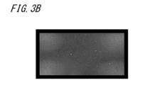
- FIG. 3B is a diagram showing a display state of a display surface when the liquid crystal display device of FIG. 3A is viewed from above.
- FIG. 4A is a diagram showing a laminated structure of a design model B of the liquid crystal display device used in the light leakage test
- FIG. 4B is a diagram showing a display state of the display surface when the liquid crystal display device of FIG. 4A is viewed from above. be.
- the inventor of the present application conducted a light transmission test on both types A and B as follows in order to confirm the presence or absence of light leakage.
- a polarizing element 10 having a base layer 8 made of a glass substrate and a metal layer 9 facing the backlight device 5 is inserted between the diffusion film 11 as a light diffusing member and the backlight device 5 as in type A.
- the surface temperature on the exit side of the liquid crystal display element 4 decreased, light leakage was still observed. It is considered that the cause is that the diffusion film 11 is locally hot, especially in the central portion rather than the peripheral portion (four corners).
- a liquid crystal display element by inserting a polarizing element 10 having a metal layer 9 whose base layer 8 faces a backlight device 5 made of a glass substrate between the incident side polarizing plate 7 and the diffusion film 14 as in type B.
- the surface temperature on the exit side of No. 4 was lowered, and the light leakage was improved.
- the thermal conductivity (0.55 to 0.75 (W / mK)) of the glass substrate constituting the polarizing element 10 is the thermal conductivity (0.12 to 0.29 (W)) of the resin material constituting the diffusion film 11. Since it is larger than / mK)) and the polarizing element 10 is closer to the liquid crystal display element 4 than the diffusion film 11, local temperature rise of the incident side polarizing plate 7 is prevented.
- FIG. 5 is a graph showing the temperature measurement result showing the effect of suppressing the temperature rise of the metal layer 9.
- the backlight device 5 irradiates the liquid crystal display element 4 with backlight light, and the display is the emission side surface of the liquid crystal display element 4 at that time.
- the temperatures of the central portion and the corner portion of the surface were measured in the case where the metal layer 9 was present and in the case where the metal layer 9 was not present, and the presence or absence of the temperature decrease and the degree of the temperature decrease were confirmed.
- ⁇ 1 indicates the difference between the temperature of the central portion of the display surface and the temperature of the corner portion when the metal layer 9 is not present
- ⁇ 2 is the temperature of the central portion of the display surface when the metal layer 9 is present. The difference from the temperature of the corner part is shown.
- the display light is projected onto the windshield, which is an example of the projection member attached to the windshield of the vehicle.
- a visual operator such as a driver can visually recognize the display light projected on the windshield by superimposing it on the actual view in front of the windshield.
- the polarizing element 10 changes the ratio of light from the backlight device 5 passing through the liquid crystal display device 1 together with the incident side polarizing plate 7.
- the polarizing element 10 has a base layer 8 formed on the basis of a glass substrate, and a thin metal wire 13 also called a metal nanowire grid is arranged on the surface portion of the base layer 8 on the backlight device 5 side, and the surface portion thereof. A fine metal slit is formed in the surface.
- the polarizing element 10 transmits a light component that vibrates in a direction along the light transmission axis, and reflects a light component that vibrates in a direction along a light reflection axis perpendicular to the light transmission axis. That is, as shown in FIG. 2 described above, the polarizing element 10 transmits the light component that vibrates in the direction orthogonal to the slit (grid) and reflects the light component that vibrates in the direction parallel to the slit (grid).
- the base layer 8 is made of a glass substrate in this embodiment, but in other embodiments, it may be a transparent resin substrate, a transparent resin sheet, or the like.
- the transparent resin refers to a resin having a total light transmittance of 70% or more measured on a plate having a thickness of 2 mm and smooth on both sides based on JIS K7361-1.
- Examples thereof include a dimethanol copolymer, polycarbonate, an acrylic resin, and a resin having an alicyclic structure.
- the transparent resin is a copolymer of polycarbonate, polystyrene, an aromatic vinyl-based monomer containing 10% or more of an aromatic vinyl monomer, and a (meth) acrylic acid alkyl ester having a lower alkyl group.
- a resin having an alicyclic structure or the like having a water absorption rate of 0.25% or less is less deformed by moisture absorption, so that the base layer 8 can obtain the same function as the large light diffusion layer 11 with less warpage. Can be done.
- a granular light diffusing agent may be mixed in the base layer 8.
- the light diffusing agent is a particle having a property of diffusing light rays, and can be roughly classified into an inorganic filler and an organic filler.
- the inorganic filler include silica, aluminum hydroxide, aluminum oxide, titanium oxide, zinc oxide, barium sulfate, magnesium silicate, and mixtures thereof.
- the organic filler include acrylic resin, polyurethane, polyvinyl chloride, polystyrene resin, polyacrylonitrile, polyamide, polysiloxane resin, melamine resin, and benzoguanamine resin.
- the shape of the light diffusing agent examples include a spherical shape, a cubic shape, a needle shape, a rod shape, a spindle shape, a plate shape, a scale shape, and a fibrous shape.
- the light diffusion direction is isotropic.
- a spherical shape is preferable because it can be formed.
- a diffusing film is produced in a state where the light diffusing agent is uniformly dispersed in the transparent resin.
- the light emitted from the backlight device 5 passes through the diffusion film (diffuser) 11 and reaches the polarizing element 10.
- the light component that vibrates in the direction along the light transmission axis of the polarizing element 10 passes through the polarizing element 10, passes through the incident side polarizing plate 7, and is incident on the liquid crystal display element 4.
- the light component that vibrates in the direction perpendicular to the light reflection axis of the polarizing element 10 is reflected by the polarizing element 10.
- the vibration direction is diffused by providing the light diffusing member 11 between the polarizing element 10 and the backlight device 5, and the polarizing element is again used. Head to 10. As a result, the light reflected by the polarizing element 10 is reused, and the amount of light is increased.
- the polarizing element 10 may be in contact with a heat conductive member such as a metal frame, a metal bezel, or a metal container that conducts and diffuses heat to the outside.
- a heat conductive member such as a metal frame, a metal bezel, or a metal container that conducts and diffuses heat to the outside.
- the conductive tape 12 may be attached to the peripheral portion of the polarizing element 10, that is, the region outside the effective display region M.
- a metal film having excellent conductivity and thermal conductivity such as Cu is applied and vapor-filmed on one surface of a resin film, and the conductive tape is formed into a rectangular flat plate shape by a conductive adhesive.
- the conductive tape 12 is a metal film having high thermal conductivity such as silver (Ag), copper (Cu), aluminum (Al), etc., on the surface of a resin sheet having a thickness of about 100 ⁇ m to 500 ⁇ m, which is made of a resin material such as acrylic resin. Is produced by forming by a vapor deposition method or the like. That is, the conductive tape 12 may be a metal sheet which is a kind of heat radiating sheet. The thermal conductivity of the metal sheet is about 230 to 400 W / (m ⁇ K).
- the conductive tape 12 may be a graphite sheet having a thickness of about 25 ⁇ m to 100 ⁇ m, which is a kind of heat dissipation sheet.
- the graphite sheet has a thermal conductivity of about 1500 W / (m ⁇ K).
- the conductive tape 12 may be attached to the metal layer 9 at the peripheral edge of the polarizing element 10. In this case, the conductive tape 12 can effectively receive heat from the metal layer 9 having high thermal conductivity.
- the conductive tape 12 may be attached to the side surfaces of the metal layer 9 and the base layer 8 at the peripheral edge of the polarizing element 10.
- the conductive tape 12 has an increased sticking area with respect to the polarizing element 10, and can receive heat more effectively from the polarizing element 10.
- the conductive tape 12 may be attached to the peripheral edge of the polarizing element 10 over the entire circumference. In this case, the heat generated by the polarizing element 10 can be uniformly dissipated to the surroundings. Further, the conductive tape 12 may be in contact with the heat conductive member over the entire circumference. In this case, the effect of uniformly dissipating the heat generated by the polarizing element 10 to the surroundings is improved.
- the conductive tape 12 may have light transmission. In this case, it is possible to prevent the conductive tape 12 from affecting the display of the liquid crystal display element 4. That is, it is possible to prevent the light transmittance of the peripheral portion of the display portion of the liquid crystal display element 4 from being lowered, the brightness of the image at the peripheral portion of the display portion being lowered, and the contrast of the image at the peripheral portion of the display portion being lowered. be able to.
- the light-transmitting conductive tape 12 can be produced by making the thickness of the metal film about 30 nm or less.
- the thickness of the metal film may be about 20 nm or less, or about 3 nm to 15 nm.
- the light transmittance of the conductive tape 12 does not have to be 100%, may be about 10% to 90%, and may be 30% to 70%. It may be about.
- the end of the metal layer of the polarizing element 10 may be in contact with the heat conductive member.
- the metal layer having high thermal conductivity comes into contact with the thermal conductive member, heat can be efficiently transferred to the thermal conductive member.
- the end of the metal layer is in contact with the heat conductive member, it is possible to prevent the heat conductive member from affecting the display of the liquid crystal display element 4.
- an extension portion formed in a band shape in the peripheral direction of the metal layer may be provided at the end of the metal layer, and the extension portion may be in contact with the heat conductive member.
- heat can be transferred to the heat conductive member more efficiently by increasing the contact area between the metal layer and the heat conductive member.
- a strip-shaped extension may be provided at the end of the metal layer over the entire circumference. Further, the edge of the base layer and the end of the metal layer of the polarizing element 10 may be in contact with the heat conductive member.
- the width of the portion of the thin metal wire 13 in contact with the heat conductive member may be larger than the width of the remaining portion. In this case, the contact area where the metal layer is in contact with the heat conductive member is increased, and heat can be transferred to the heat conductive member more efficiently.
- the polarizing element 10 may have a configuration in which the size thereof is larger than the size of the liquid crystal display element 4 in a plan view. In this case, the heat capacity of the polarizing element 10 is increased, and the polarizing element 10 can receive the light radiated from the backlight device 5 to more effectively store the radiant heat and insulate it. Further, as shown in FIG. 8, the polarizing element 10 has a configuration in which the size thereof is larger than the size of the liquid crystal display element 4 in a plan view, and the polarizing element 10 includes the liquid crystal display element 4 in a plan view. There may be. In this case, the thermal influence of the polarizing element 10 on the liquid crystal display element 4 is not biased and tends to be uniform.
- the size (area) of the polarizing element 10 in a plan view may be more than 1 times and not more than 1.5 times the size (area) of the liquid crystal display element 4 in a plan view, and may be more than 1 times and 1 It may be about 3 or less.
- the polarizing element 10 may have a configuration in which the size thereof is smaller than the size of the liquid crystal display element 4 in a plan view and has a size equal to or larger than the effective display area of the display unit of the liquid crystal display element 4.
- the polarizing element 10 is made smaller and lighter, the liquid crystal display device 1 is made lighter and cheaper.
- the size of the heat conductive member can be relatively increased in the plan view by the amount that the size of the polarizing element 10 in the plan view is reduced. As a result, the heat dissipation of the polarizing element 10 can be improved.
- the conductive tape 12 may be attached only to the side surface of the base layer of the polarizing element 10. With this configuration, it is possible to prevent the conductive tape 12 from affecting the display image of the liquid crystal display element 4.
- the size (area) of the polarizing element 10 in a plan view may be about 0.8 times or more and less than 1 times the size (area) of the liquid crystal display element 4 in a plan view, and is about 0.9 times or more. It may be less than one time.
- the polarizing element 10 is located on the side surface of the base layer 8 rather than the surface roughness (arithmetic mean roughness) of one main surface (for example, the upper surface) and the other main surface (for example, the lower surface) of the base layer 8.
- the structure may have a large surface roughness (arithmetic mean roughness).
- the surface area of the side surface of the base layer 8 is increased, and heat can be dissipated more efficiently. Further, when the side surface of the base layer 8 is in contact with the heat conductive member, heat can be transferred to the heat conductive member more efficiently.
- the side surface of the base layer 8 may be bonded to the heat conductive member via a bonding member of a type that is applied and cured, such as an adhesive.
- the joining member penetrates into the fine irregularities on the side surface of the base layer 8, and the joining member can efficiently receive heat from the side surface of the base layer 8.
- the joining member may include a thermally conductive member having high thermal conductivity such as metal particles.
- the polarizing element 10 has a configuration in which the arithmetic mean roughness of the side surface of the base layer 8 is larger than the arithmetic mean roughness of one main surface and the other main surface of the base layer 8, and the metal layer 9 and the base layer 8 are formed.
- the conductive tape 12 may be in contact with or bonded to the side surface of the tape. In this case, the contact area or the bonding area between the side surface of the base layer 8 and the conductive tape 12 is increased, and the heat of the polarizing element 10 can be effectively transferred to the conductive tape 12.
- the conductive tape 12 When the conductive tape 12 is bonded to the side surface of the base layer 8, it may be bonded via a bonding agent such as an adhesive or an adhesive. Further, the bonding agent may contain a thermally conductive member having high thermal conductivity such as metal particles.
- the arithmetic average roughness of one main surface and the other main surface of the base layer 8 may be about 1 nm to 100 nm, respectively, and the arithmetic average roughness of the side surface of the base layer 8 may be about 100 nm to 500 nm.
- the arithmetic mean roughness can be adjusted by adjusting the size of the count (average particle size) of the abrasives such as alumina abrasives and diamond abrasives when the surface to be ground is ground.
- the light diffusing member 11 may be in contact with a heat conductive member such as a metal frame, a metal bezel, or a metal container that conducts and diffuses heat to the outside.
- a heat conductive member such as a metal frame, a metal bezel, or a metal container that conducts and diffuses heat to the outside.
- the end of the light diffusing member 11 may be in contact with the heat conductive member. In this case, it is possible to prevent the heat conductive member from affecting the display of the liquid crystal display element 4. Further, an extension portion formed in a band shape in the peripheral direction of the light diffusion member 11 may be provided at the end of the light diffusion member 11, and the extension portion may be in contact with the heat conductive member. In this case, heat can be transferred to the heat conductive member more efficiently by increasing the contact area between the light diffusion member 11 and the heat conductive member. In order to achieve this purpose more effectively, a band-shaped extending portion may be provided on the entire circumference of the end of the light diffusing member 11.
- the above-mentioned emitting side polarizing plate 6 is adhered to the emitting side surface of the liquid crystal display element 4 with a transparent adhesive
- the above-mentioned incident side polarizing plate 7 is adhered to the incident side surface of the liquid crystal display element 4 with a transparent adhesive.
- the above-mentioned light diffusing member 11 may be adhered to the incident side polarizing plate 7 with a transparent adhesive
- the polarizing element 10 may be adhered to the light diffusing member 11 with a transparent adhesive.
- These adhesions are optical bonding using an optically elastic resin.
- a transparent optical adhesive for example, an OCA functional film (OCA; Optical Clear Adhesive), an adhesive adhesive (OCR; Optical Clear Resin), or the like may be used.
- the adhesive may contain a diffusing agent, if necessary.
- the material as the diffusing agent is not particularly limited, and inorganic and organic diffusing agents can be appropriately selected and used.
- Inorganic diffusers consist of glass, silicon oxide, aluminum hydroxide, aluminum oxide, titanium oxide, zinc oxide, barium sulfate, magnesium silicate, etc .; organic diffusers include fluororesins, polystyrene resins, acrylic resins, polycarbonates, etc.
- Examples include resins, silicone resins, polyethylene resins, ethylene-vinyl acetate copolymers, acrylonitrile, polyurethane, polyvinyl chloride, polyacrylonitrile, polyamide, polysiloxane resin, melamine resin, benzoguanamine resin, and crosslinked products thereof. Be done.
- the shape of the diffusing agent is not particularly limited, and examples thereof include a spherical shape, an ellipsoidal shape, a cubic shape, a needle shape, a rod shape, a spindle shape, a plate shape, a scaly shape, and a fibrous shape.
- a spherical shape or an ellipsoidal shape close to a spherical shape is preferable in terms of anisotropic shape.
- the refractive index of the diffusing agent is preferably different from the refractive index of the main polymer used as the base material of the adhesive composition, and the difference in refractive index is preferably 0.05 or more and 0.15 or less.
- the refractive index difference is less than 0.05, the light diffusion effect is insufficient, and when the refractive index difference exceeds 0.15, the light diffusion effect is improved, but the transmittance of obliquely incident light to the diffusion adhesive layer is improved. Is not preferable because it decreases and becomes dark as a whole.
- the temperature rise of the liquid crystal display element 4 due to the high temperature of the backlight device 5 is suppressed, the light leakage of the black display of the projected image by the liquid crystal display device 1 is prevented, and the sense of reality is not impaired.
- An image of quality can be displayed.
- the liquid crystal display device of the present disclosure can be applied to various electronic devices.
- the electronic devices include head-up display devices such as AR-HUD, digital display watches such as smart watches, automobile route guidance systems (car navigation systems), ship route guidance systems, aircraft route guidance systems, smartphone terminals, and mobile phones.
- Tablet terminal personal digital assistant (PDA), video camera, digital still camera, electronic notebook, electronic book, electronic dictionary, personal computer, copying machine, terminal device of game equipment, television, product display tag, price display tag, Industrial programmable display device, car audio, digital audio player, facsimile, printer, automatic cash deposit / payment machine (ATM), vending machine, head-mounted display device (HMD), bus, train Examples include an advertisement display device in a vehicle such as a vehicle, a guidance display device installed at a station, an airport, or the like.
Landscapes
- Physics & Mathematics (AREA)
- Nonlinear Science (AREA)
- Chemical & Material Sciences (AREA)
- Mathematical Physics (AREA)
- Crystallography & Structural Chemistry (AREA)
- General Physics & Mathematics (AREA)
- Optics & Photonics (AREA)
- Liquid Crystal (AREA)
- Inorganic Chemistry (AREA)
- Eyeglasses (AREA)
- Polarising Elements (AREA)
Priority Applications (3)
| Application Number | Priority Date | Filing Date | Title |
|---|---|---|---|
| JP2022517583A JP7385020B2 (ja) | 2020-04-28 | 2021-04-06 | 液晶表示装置 |
| US17/921,937 US12019334B2 (en) | 2020-04-28 | 2021-04-06 | Liquid crystal display device |
| CN202180031096.6A CN115461674B (zh) | 2020-04-28 | 2021-04-06 | 液晶显示装置 |
Applications Claiming Priority (2)
| Application Number | Priority Date | Filing Date | Title |
|---|---|---|---|
| JP2020079554 | 2020-04-28 | ||
| JP2020-079554 | 2020-04-28 |
Publications (1)
| Publication Number | Publication Date |
|---|---|
| WO2021220738A1 true WO2021220738A1 (ja) | 2021-11-04 |
Family
ID=78373490
Family Applications (1)
| Application Number | Title | Priority Date | Filing Date |
|---|---|---|---|
| PCT/JP2021/014663 Ceased WO2021220738A1 (ja) | 2020-04-28 | 2021-04-06 | 液晶表示装置 |
Country Status (4)
| Country | Link |
|---|---|
| US (1) | US12019334B2 (https=) |
| JP (1) | JP7385020B2 (https=) |
| CN (1) | CN115461674B (https=) |
| WO (1) | WO2021220738A1 (https=) |
Families Citing this family (1)
| Publication number | Priority date | Publication date | Assignee | Title |
|---|---|---|---|---|
| CN115826283B (zh) * | 2022-12-12 | 2025-10-10 | 芜湖汽车前瞻技术研究院有限公司 | 显示屏、抬头显示器及车辆 |
Citations (10)
| Publication number | Priority date | Publication date | Assignee | Title |
|---|---|---|---|---|
| JPH09113906A (ja) * | 1995-10-13 | 1997-05-02 | Sony Corp | 透過型表示装置 |
| JP2006323351A (ja) * | 2005-05-16 | 2006-11-30 | Lg Electronics Inc | 偏光シートの製造方法及びその偏光シートを備えたディスプレイ装置 |
| WO2009101797A1 (ja) * | 2008-02-13 | 2009-08-20 | Sharp Kabushiki Kaisha | 照明装置および液晶表示装置 |
| JP2009222980A (ja) * | 2008-03-17 | 2009-10-01 | Seiko Epson Corp | 電気光学装置及び電子機器 |
| JP2010176879A (ja) * | 2009-01-27 | 2010-08-12 | Nippon Zeon Co Ltd | バックライトユニット及び液晶表示装置 |
| JP2014052439A (ja) * | 2012-09-05 | 2014-03-20 | Dexerials Corp | 偏光素子、プロジェクター及び偏光素子の製造方法 |
| WO2018225655A1 (ja) * | 2017-06-09 | 2018-12-13 | スタンレー電気株式会社 | 車両用前照灯システム |
| CN109270727A (zh) * | 2018-11-23 | 2019-01-25 | 天马微电子股份有限公司 | 显示面板以及电子设备 |
| JP2020021066A (ja) * | 2018-08-02 | 2020-02-06 | クリスティ デジタル システムズ ユーエスエイ インコーポレイテッド | 三次元画像を生成するためのモノリシック・ワイヤグリッド偏光子を有する発光ダイオードディスプレイ |
| JP2020042234A (ja) * | 2018-09-13 | 2020-03-19 | セイコーエプソン株式会社 | 電気光学装置および電子機器 |
Family Cites Families (7)
| Publication number | Priority date | Publication date | Assignee | Title |
|---|---|---|---|---|
| JP2008268940A (ja) * | 2007-03-27 | 2008-11-06 | Toray Ind Inc | 反射型偏光板及びそれを用いた液晶表示装置 |
| CN102224158B (zh) * | 2008-11-21 | 2015-09-16 | 日本化药株式会社 | 新的杂环化合物及其用途 |
| JP6135048B2 (ja) | 2012-04-24 | 2017-05-31 | 日本精機株式会社 | ヘッドアップディスプレイ装置 |
| TWM476931U (en) * | 2013-12-10 | 2014-04-21 | Applied Green Light Taiwan Inc | Liquid crystal display device |
| CN204405992U (zh) * | 2015-03-03 | 2015-06-17 | 信利半导体有限公司 | 一种液晶显示屏 |
| CN110320696A (zh) * | 2018-03-29 | 2019-10-11 | 夏普株式会社 | 液晶显示装置 |
| CN108919496A (zh) * | 2018-08-08 | 2018-11-30 | 京东方科技集团股份有限公司 | 防太阳辐射的低功耗hud系统 |
-
2021
- 2021-04-06 JP JP2022517583A patent/JP7385020B2/ja active Active
- 2021-04-06 US US17/921,937 patent/US12019334B2/en active Active
- 2021-04-06 WO PCT/JP2021/014663 patent/WO2021220738A1/ja not_active Ceased
- 2021-04-06 CN CN202180031096.6A patent/CN115461674B/zh active Active
Patent Citations (10)
| Publication number | Priority date | Publication date | Assignee | Title |
|---|---|---|---|---|
| JPH09113906A (ja) * | 1995-10-13 | 1997-05-02 | Sony Corp | 透過型表示装置 |
| JP2006323351A (ja) * | 2005-05-16 | 2006-11-30 | Lg Electronics Inc | 偏光シートの製造方法及びその偏光シートを備えたディスプレイ装置 |
| WO2009101797A1 (ja) * | 2008-02-13 | 2009-08-20 | Sharp Kabushiki Kaisha | 照明装置および液晶表示装置 |
| JP2009222980A (ja) * | 2008-03-17 | 2009-10-01 | Seiko Epson Corp | 電気光学装置及び電子機器 |
| JP2010176879A (ja) * | 2009-01-27 | 2010-08-12 | Nippon Zeon Co Ltd | バックライトユニット及び液晶表示装置 |
| JP2014052439A (ja) * | 2012-09-05 | 2014-03-20 | Dexerials Corp | 偏光素子、プロジェクター及び偏光素子の製造方法 |
| WO2018225655A1 (ja) * | 2017-06-09 | 2018-12-13 | スタンレー電気株式会社 | 車両用前照灯システム |
| JP2020021066A (ja) * | 2018-08-02 | 2020-02-06 | クリスティ デジタル システムズ ユーエスエイ インコーポレイテッド | 三次元画像を生成するためのモノリシック・ワイヤグリッド偏光子を有する発光ダイオードディスプレイ |
| JP2020042234A (ja) * | 2018-09-13 | 2020-03-19 | セイコーエプソン株式会社 | 電気光学装置および電子機器 |
| CN109270727A (zh) * | 2018-11-23 | 2019-01-25 | 天马微电子股份有限公司 | 显示面板以及电子设备 |
Also Published As
| Publication number | Publication date |
|---|---|
| JP7385020B2 (ja) | 2023-11-21 |
| US20230176422A1 (en) | 2023-06-08 |
| US12019334B2 (en) | 2024-06-25 |
| CN115461674B (zh) | 2025-01-28 |
| CN115461674A (zh) | 2022-12-09 |
| JPWO2021220738A1 (https=) | 2021-11-04 |
Similar Documents
| Publication | Publication Date | Title |
|---|---|---|
| CN101055324B (zh) | 光学片、背光装置及液晶显示装置 | |
| US9176264B2 (en) | Light-diffusing element, polarizing plate having light-diffusing element attached thereto, polarizing element, and liquid crystal display device equipped with those components | |
| WO2015046439A1 (ja) | プリズムシート、面光源装置、映像源ユニット、及び液晶表示装置 | |
| US20120019758A1 (en) | Display device | |
| JP6004060B2 (ja) | 映像源ユニット、及び表示装置 | |
| JP4423933B2 (ja) | 光学シートとそれを用いたバックライトユニットおよびディスプレイ | |
| KR20080012340A (ko) | 광확산판과 그 제조 방법 | |
| JP4039465B1 (ja) | 光学シートとそれを用いたバックライトユニット及びディスプレイ | |
| JP6880612B2 (ja) | 映像源ユニット、及び表示装置 | |
| JP6933005B2 (ja) | 光学シート、映像源ユニット及び液晶表示装置 | |
| US12235531B2 (en) | Glass backplane and method of manufacturing the same, and display apparatus | |
| JP7385020B2 (ja) | 液晶表示装置 | |
| US8638409B2 (en) | Dual liquid crystal display | |
| JP5287147B2 (ja) | 光学シート、及び映像表示装置 | |
| JP2015180952A (ja) | プリズムシート、面光源装置、映像源ユニット、及び液晶表示装置 | |
| JP2018112618A (ja) | 映像源ユニット、及び表示装置 | |
| JP2016212191A (ja) | プリズムシート、面光源装置、映像源ユニット、及び液晶表示装置 | |
| JP2018106109A (ja) | 映像源ユニット、表示装置 | |
| JP6083301B2 (ja) | 映像源ユニット、液晶表示装置 | |
| JP6110826B2 (ja) | プリズムシート、面光源装置、映像源ユニット、及び液晶表示装置 | |
| JP2015087766A (ja) | プリズムシート、面光源装置、映像源ユニット、及び液晶表示装置 | |
| JP5803242B2 (ja) | 面光源装置及び液晶表示装置 | |
| JP2018055062A (ja) | 反射シート、面光源装置、映像源ユニット、及び液晶表示装置 | |
| JP2017198974A (ja) | 光学ユニット、面光源装置、映像源ユニット、及び液晶表示装置 | |
| JP2012003971A (ja) | 面光源装置用積層体、面光源装置及び液晶表示装置 |
Legal Events
| Date | Code | Title | Description |
|---|---|---|---|
| 121 | Ep: the epo has been informed by wipo that ep was designated in this application |
Ref document number: 21795290 Country of ref document: EP Kind code of ref document: A1 |
|
| ENP | Entry into the national phase |
Ref document number: 2022517583 Country of ref document: JP Kind code of ref document: A |
|
| NENP | Non-entry into the national phase |
Ref country code: DE |
|
| 122 | Ep: pct application non-entry in european phase |
Ref document number: 21795290 Country of ref document: EP Kind code of ref document: A1 |
|
| WWG | Wipo information: grant in national office |
Ref document number: 202180031096.6 Country of ref document: CN |