US8638409B2 - Dual liquid crystal display - Google Patents
Dual liquid crystal display Download PDFInfo
- Publication number
- US8638409B2 US8638409B2 US13/044,058 US201113044058A US8638409B2 US 8638409 B2 US8638409 B2 US 8638409B2 US 201113044058 A US201113044058 A US 201113044058A US 8638409 B2 US8638409 B2 US 8638409B2
- Authority
- US
- United States
- Prior art keywords
- display panel
- light
- lgp
- light source
- lcd
- Prior art date
- Legal status (The legal status is an assumption and is not a legal conclusion. Google has not performed a legal analysis and makes no representation as to the accuracy of the status listed.)
- Expired - Fee Related, expires
Links
Images


Classifications
-
- G—PHYSICS
- G02—OPTICS
- G02F—OPTICAL DEVICES OR ARRANGEMENTS FOR THE CONTROL OF LIGHT BY MODIFICATION OF THE OPTICAL PROPERTIES OF THE MEDIA OF THE ELEMENTS INVOLVED THEREIN; NON-LINEAR OPTICS; FREQUENCY-CHANGING OF LIGHT; OPTICAL LOGIC ELEMENTS; OPTICAL ANALOGUE/DIGITAL CONVERTERS
- G02F1/00—Devices or arrangements for the control of the intensity, colour, phase, polarisation or direction of light arriving from an independent light source, e.g. switching, gating or modulating; Non-linear optics
- G02F1/01—Devices or arrangements for the control of the intensity, colour, phase, polarisation or direction of light arriving from an independent light source, e.g. switching, gating or modulating; Non-linear optics for the control of the intensity, phase, polarisation or colour
- G02F1/13—Devices or arrangements for the control of the intensity, colour, phase, polarisation or direction of light arriving from an independent light source, e.g. switching, gating or modulating; Non-linear optics for the control of the intensity, phase, polarisation or colour based on liquid crystals, e.g. single liquid crystal display cells
- G02F1/133—Constructional arrangements; Operation of liquid crystal cells; Circuit arrangements
- G02F1/1333—Constructional arrangements; Manufacturing methods
- G02F1/1335—Structural association of cells with optical devices, e.g. polarisers or reflectors
- G02F1/1336—Illuminating devices
- G02F1/133615—Edge-illuminating devices, i.e. illuminating from the side
-
- G—PHYSICS
- G02—OPTICS
- G02B—OPTICAL ELEMENTS, SYSTEMS OR APPARATUS
- G02B6/00—Light guides; Structural details of arrangements comprising light guides and other optical elements, e.g. couplings
- G02B6/0001—Light guides; Structural details of arrangements comprising light guides and other optical elements, e.g. couplings specially adapted for lighting devices or systems
- G02B6/0011—Light guides; Structural details of arrangements comprising light guides and other optical elements, e.g. couplings specially adapted for lighting devices or systems the light guides being planar or of plate-like form
- G02B6/0033—Means for improving the coupling-out of light from the light guide
- G02B6/0063—Means for improving the coupling-out of light from the light guide for extracting light out both the major surfaces of the light guide
-
- G—PHYSICS
- G02—OPTICS
- G02F—OPTICAL DEVICES OR ARRANGEMENTS FOR THE CONTROL OF LIGHT BY MODIFICATION OF THE OPTICAL PROPERTIES OF THE MEDIA OF THE ELEMENTS INVOLVED THEREIN; NON-LINEAR OPTICS; FREQUENCY-CHANGING OF LIGHT; OPTICAL LOGIC ELEMENTS; OPTICAL ANALOGUE/DIGITAL CONVERTERS
- G02F1/00—Devices or arrangements for the control of the intensity, colour, phase, polarisation or direction of light arriving from an independent light source, e.g. switching, gating or modulating; Non-linear optics
- G02F1/01—Devices or arrangements for the control of the intensity, colour, phase, polarisation or direction of light arriving from an independent light source, e.g. switching, gating or modulating; Non-linear optics for the control of the intensity, phase, polarisation or colour
- G02F1/13—Devices or arrangements for the control of the intensity, colour, phase, polarisation or direction of light arriving from an independent light source, e.g. switching, gating or modulating; Non-linear optics for the control of the intensity, phase, polarisation or colour based on liquid crystals, e.g. single liquid crystal display cells
- G02F1/133—Constructional arrangements; Operation of liquid crystal cells; Circuit arrangements
- G02F1/1333—Constructional arrangements; Manufacturing methods
- G02F1/133342—Constructional arrangements; Manufacturing methods for double-sided displays
-
- G—PHYSICS
- G02—OPTICS
- G02F—OPTICAL DEVICES OR ARRANGEMENTS FOR THE CONTROL OF LIGHT BY MODIFICATION OF THE OPTICAL PROPERTIES OF THE MEDIA OF THE ELEMENTS INVOLVED THEREIN; NON-LINEAR OPTICS; FREQUENCY-CHANGING OF LIGHT; OPTICAL LOGIC ELEMENTS; OPTICAL ANALOGUE/DIGITAL CONVERTERS
- G02F1/00—Devices or arrangements for the control of the intensity, colour, phase, polarisation or direction of light arriving from an independent light source, e.g. switching, gating or modulating; Non-linear optics
- G02F1/01—Devices or arrangements for the control of the intensity, colour, phase, polarisation or direction of light arriving from an independent light source, e.g. switching, gating or modulating; Non-linear optics for the control of the intensity, phase, polarisation or colour
- G02F1/13—Devices or arrangements for the control of the intensity, colour, phase, polarisation or direction of light arriving from an independent light source, e.g. switching, gating or modulating; Non-linear optics for the control of the intensity, phase, polarisation or colour based on liquid crystals, e.g. single liquid crystal display cells
- G02F1/133—Constructional arrangements; Operation of liquid crystal cells; Circuit arrangements
- G02F1/1333—Constructional arrangements; Manufacturing methods
- G02F1/1335—Structural association of cells with optical devices, e.g. polarisers or reflectors
- G02F1/1336—Illuminating devices
- G02F1/133616—Front illuminating devices
Definitions
- the present invention relates to a liquid crystal display (LCD), and more particularly, to a dual LCD which displays images on both surfaces thereof.
- LCD liquid crystal display
- liquid crystal displays Being slim, lightweight, and low in power consumption, liquid crystal displays (LCDs) are extensively used in the industries of monitors, notebooks, mobile phones, and the like. LCDs have also been used as digital information displays (DIDs). DIDs are devices that display advertisements and information in public places, such as airports, subway stations, large shopping malls , and movie theaters. Unlike conventional electronic display boards and billboards with limited resolution and color representation, DIDs can display various types of information including digital moving images.
- DIDs digital information displays
- Dual LCDs that may display the same image or different images on both surfaces thereof, for example, front and back surfaces, may be used for DIDs.
- Embodiments of the present invention provide a liquid crystal display (LCD) which can be operated with low power consumption and exhibits increased luminance uniformity.
- LCD liquid crystal display
- an LCD including at least one light source which provides light, a display panel which includes pixels reflecting the light from the light source, and at least one light guide plate (LGP) which is formed substantially parallel to a surface of the display panel and is separated from the display panel, wherein a predetermined space is defined between the LGP and the display panel, and the LGP guides the light emitted from the light source to the pixels and allows the light reflected by the pixels to pass through the LGP.
- LGP light guide plate
- an LCD including at least one light source which provides light, a display panel which includes pixels reflecting the light from the light source, and at least one optical path controller which is disposed in an optical path between the light source and the pixels of the display panel and controls a path of the light emitted from the light source to proceed to the pixels of the display panel.
- FIG. 1A is a side view of a transmissive liquid crystal display (LCD);
- FIG. 1B is a side view of a reflective LCD
- FIG. 2 is a side view of a dual reflective LCD according to an exemplary embodiment of the present invention.
- FIG. 3A is a front view of an LCD according to an exemplary embodiment of the present invention.
- FIG. 3B is a front view of the LCD of FIG. 3A , illustrating the arrangement of a display panel and light sources;
- FIGS. 4A and 4B are side views of LCDs according to some exemplary embodiment of the present invention.
- FIG. 5 is a side view of an LCD according to an exemplary embodiment of the present invention.
- FIGS. 6A through 6I are views showing the shape of an optical path controller according to various exemplary embodiments of the present invention.
- FIG. 7 is a view showing optical path controllers and a display panel according to an exemplary embodiment of the present invention.
- FIG. 8 is a side view of an LCD according to an exemplary embodiment of the present invention.
- FIG. 9 is a side view of an LCD according to an exemplary embodiment of the present invention.
- FIG. 1A is a side view of a transmissive liquid crystal display (LCD).
- the transmissive LCD includes a display panel 100 which includes one or more pixels and a light unit 200 which is parallel to a surface of the display panel 100 .
- the transmissive LCD light emitted from the light unit 200 passes through the display panel 100 to be seen from a viewer's side.
- the pixels of the display panel 200 allow light emitted from the light unit 200 to pass therethrough in equal or different amounts, with the transmittance of each pixel controlled, so that the combination of the pixels displays an image.
- a light unit may be located behind an LCD panel as seen from the position of a viewer.
- the light unit is also referred to as a backlight unit.
- FIG. 1B is a side view of a reflective LCD.
- a light unit 200 is located between a viewer (not shown) and a display panel 100 . Light emitted from the light unit 200 is incident upon the display panel 100 and is reflected by each pixel of the display panel 100 . Then, the reflected light passes through the light unit 200 toward the viewer's side.
- the pixels of the display panel 200 reflect light from the light unit 200 in equal or different amounts, with the reflectivity of each pixel controlled, so that the combination of the pixels displays an image.
- a light unit may be located in front of an LCD panel as viewed from the position of a viewer. The light unit is also referred to as a front light unit.
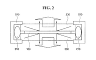
- FIG. 2 is a side view of a dual reflective LCD according to an exemplary embodiment of the present invention.
- light emitted from light sources 210 may pass through light guide plates (LGPs) 230 to a display panel 100 .
- the LGPs 230 may contact the display panel 100 .
- the light sources 210 may be located on sides of the display panel 100 as shown in FIG. 2 , and light emitted from the light sources 210 can be uniformly delivered to all regions of the display panel 100 by the LGPs 230 .
- Light emitted from the light sources 210 arrives at each pixel of the display panel 100 via the LGPs 230 . Then, the pixels of the display panel 100 reflect the light in equal or different amounts, thereby forming an image.
- One LGP 230 may be installed either in front of or behind the display panel 100 .
- two LGPs 230 may respectively be installed both in front of and behind the display panel 100 .
- the LGPs 230 are respectively installed both in front of and behind the display panel 100 , light can be uniformly input to the display panel 100 from the front and rear sides of the display panel 100 . Accordingly, the image quality can be improved on both front and rear sides of the display panel 100 .
- the light sources 210 may be located on sides of the display panel 100 .
- the light sources 210 may be located within a structure formed in a region around the display panel 100 , for example, within a chassis 220 .
- FIG. 3A is a front view of an LCD 10 according to an exemplary embodiment of the present invention.
- FIG. 3B is a front view of the LCD 10 of FIG. 3A , illustrating the arrangement of a display panel 100 and light sources 210 .
- the LCD 10 includes a display panel 100 .
- the display panel 100 may be a transmissive LCD panel, a semi-transmissive LCD panel, or a reflective LCD panel.
- the display panel 100 may include two or more unit display panels.
- a first unit display panel may display an image on a front surface thereof
- a second unit display panel may display an image on a rear surface thereof. Images displayed on the first and second unit display panels may be identical or different.
- the display panel 100 may include one unit display panel.
- the unit display panel may display images on both surfaces thereof, for example, front and back surfaces, so that the LCD 10 can be utilized as a dual LCD.
- images displayed on both surfaces of the display panel 100 may be identical or different.
- the LCD 10 may further include a structure, such as the chassis 220 , formed in a region around the display panel 100 .
- the light sources 210 may be installed in the region where the chassis 220 is formed. If the light sources 210 are installed in the region around the display panel 100 , for example, within the chassis 220 , light emitted from the light sources 210 may be invisible to the naked eye.
- the light sources 210 may respectively be formed along four sides 251 , 252 , 253 , and 254 of the display panel 100 .
- the light sources 210 may be formed at some or all of the four sides 251 , 252 , 253 , and 254 .
- the light sources 210 may be formed at only one of the four sides 251 , 252 , 253 , and 254 or at two or more of the four sides 251 , 252 , 253 , and 254 .
- the light sources 210 are located within the chassis 220 regardless of along which of the four sides 251 , 252 , 253 , and 254 the light sources 210 are formed. Accordingly, light emitted from the light sources 210 can be prevented from being seen with the naked eye.
- FIGS. 4A and 4B are side views of LCDs 11 and 12 according to some exemplary embodiments of the present invention.
- each of the LCDs 11 and 12 includes at least one light source 210 which provides light, a display panel 100 which includes pixels reflecting light emitted from the light source 210 , and at least one LGP 231 which is separated from the display panel 100 and is substantially parallel to a surface of the display panel 100 .
- the light source 210 provides light to the display panel 100 .
- the light source 210 may be a cold cathode fluorescent lamp (CCFL), a light-emitting diode (LED), or any other optical element that emits light.
- CCFL cold cathode fluorescent lamp
- LED light-emitting diode
- the display panel 100 may be a dual LCD panel which receives light from the light source 210 and reflects light off both surfaces thereof. Since the display panel 100 has been described above with reference to FIG. 3A , a detailed description thereof will be omitted.
- the LGP 231 reflects light emitted from the light source 210 towards the pixels of the display panel 100 . Then, the LGP 231 allows the light reflected by the pixels to pass through the LGP 231 , thereby enabling each of the LCDs 11 and 12 to display an image.
- the LGP 231 and the display panel 100 are separated from each other, leaving a space 240 between the LGP 231 and the display panel 100 .
- the space 240 may be, e.g., an air gap containing air.
- the space 240 may further contain other materials in addition to air. Due to the characteristics of the air and materials introduced into the space 240 , heat released from the display panel 100 can be effectively delivered out of each of the LCDs 11 and 12 . Furthermore, as the air and the materials introduced into the spaces 240 circulate, heat released from the display panel 100 can be more effectively dissipated out of each of the LCDs 11 and 12 . Therefore, the deformation or malfunction of the display panel 100 resulting from heat accumulated in the display panel 100 can be reduced.
- the LGP 231 and the space 240 may be formed on only one surface of the display panel 100 as shown in FIG. 4A or may be formed on both surfaces of the display panel 100 as shown in FIG. 4B .
- the LGP 231 may be made of transparent plastic or glass.
- the LGP 231 made of glass can function as a protective glass plate of the display panel 100 . Accordingly, a protective glass plate to protect the display panel 100 can be omitted from the LCDs 11 and 12 .
- FIG. 5 is a side view of an LCD 13 according to an exemplary embodiment of the present invention.
- the LCD 13 includes at least one light source 210 which provides light, a display panel 100 which includes pixels reflecting light emitted from the light source 210 , and an optical path controller 232 .
- the light source 210 and the display panel 100 are substantially identical to those according to the previous embodiments and thus their descriptions will not be repeated.
- the optical path controller 232 is disposed in an optical path between the light source 210 and the pixels of the display panel 100 . Accordingly, the optical path controller 232 controls the path of light emitted from the light source 210 such that light can be delivered to the pixels of the display panel 100 .
- the optical path controller 232 may change the path of light received from the light source 210 by refracting light.
- the optical path controller 232 may refract incident light to the pixels of the display panel 100 . If the angle of refraction is controlled by finely adjusting the material and shape of the optical path controller 232 , incident light can be uniformly delivered to the entire surface of the display panel 100 . That is, the optical path controller 232 can substantially function as a light guide.
- FIGS. 6A through 6I are views illustrating the shape of an optical path controller according to various exemplary embodiments of the present invention.
- the optical path controller can have a varied number of sides, various surface forms (a flat surface or a curved surface), and various sizes.
- the optical path controller may also be horizontally symmetrical.
- the optical path controller is not limited to the shape shown in FIGS. 6A through 6I and may have other shapes.
- FIG. 7 is a view illustrating optical path controllers 232 and a display panel 100 according to an exemplary embodiment of the present invention.
- the optical path controllers 232 may respectively be formed on two sides of the display panel 100 . Further, the optical path controllers 232 may be formed adjacent to light sources 210 . As shown in FIG. 7 , each of the optical path controllers 232 is formed as a single body along a side of the display panel 100 . However, the embodiments of the present invention are not limited thereto.
- Each of the optical path controllers 232 may also be divided into one or more block regions corresponding respectively to one or more regions of the light sources 210 .
- FIG. 8 is a side view of an LCD 14 according to an exemplary embodiment of the present invention.
- the current embodiment is different from the embodiment described in connection with FIG. 7 in that the LCD 14 further includes an LGP 230 formed substantially parallel to a surface of a display panel 100 .
- the LGP 230 is formed on only one surface of the display panel 100 .
- the LGP 230 may also be formed on two surfaces of the display panel 100 . If both the optical path controller 232 and the LGP 230 are provided as in the current exemplary embodiment, light can be efficiently and uniformly diffused over the entire surface of the display panel 100 .
- FIG. 9 is a side view of an LCD 15 according to an exemplary embodiment of the present invention.
- the LCD 15 further includes an LGP 231 formed substantially parallel to a surface of the display panel 100 but are different in that the LGP 231 is separated from the display panel 100 to define a space 240 .
- the LGP 231 is formed on only one surface of the display panel 100 .
- the LGP 231 may also be formed on two surfaces of the display panel 100 . If both the optical path controller 232 and the LGP 230 are provided as in the current exemplary embodiment, light can be efficiently and uniformly diffused over the entire surface of the display panel 100 .
- the space 240 between the display panel 100 and the LGP 231 can facilitate the dissipation of heat from the display panel 100 .
- an LGP is formed on one side of a display panel to be separated from the display panel by a predetermined gap and to be parallel to the display panel.
- the LGP can deliver incident light to the entire region of the display panel and protect the display panel against internal and external physical forces.
- a cooling air circulation passage formed between the LGP and the display panel can contribute to the dissipation of heat from an LCD.
- an optical path controller is formed in an optical path between a light source and the display panel to be perpendicular to a surface of the display panel. The optical path controller controls light emitted from the light source to be delivered more uniformly to the entire region of the display panel.
Landscapes
- Physics & Mathematics (AREA)
- Nonlinear Science (AREA)
- Mathematical Physics (AREA)
- Chemical & Material Sciences (AREA)
- Crystallography & Structural Chemistry (AREA)
- General Physics & Mathematics (AREA)
- Optics & Photonics (AREA)
- Liquid Crystal (AREA)
- Devices For Indicating Variable Information By Combining Individual Elements (AREA)
- Planar Illumination Modules (AREA)
Abstract
Description
Claims (18)
Applications Claiming Priority (2)
| Application Number | Priority Date | Filing Date | Title |
|---|---|---|---|
| KR1020100025764A KR20110106616A (en) | 2010-03-23 | 2010-03-23 | Interactive liquid crystal display |
| KR10-2010-0025764 | 2010-03-23 |
Publications (2)
| Publication Number | Publication Date |
|---|---|
| US20110234943A1 US20110234943A1 (en) | 2011-09-29 |
| US8638409B2 true US8638409B2 (en) | 2014-01-28 |
Family
ID=44656066
Family Applications (1)
| Application Number | Title | Priority Date | Filing Date |
|---|---|---|---|
| US13/044,058 Expired - Fee Related US8638409B2 (en) | 2010-03-23 | 2011-03-09 | Dual liquid crystal display |
Country Status (2)
| Country | Link |
|---|---|
| US (1) | US8638409B2 (en) |
| KR (1) | KR20110106616A (en) |
Families Citing this family (5)
| Publication number | Priority date | Publication date | Assignee | Title |
|---|---|---|---|---|
| KR20110106616A (en) * | 2010-03-23 | 2011-09-29 | 삼성전자주식회사 | Interactive liquid crystal display |
| KR20130110491A (en) | 2012-03-29 | 2013-10-10 | 삼성디스플레이 주식회사 | Liquid crystal display device |
| CN106292060B (en) * | 2015-12-15 | 2020-04-07 | 宋义 | Luminous liquid crystal panel, liquid crystal display device and foreground light source of display terminal |
| CN106292059B (en) * | 2015-12-15 | 2020-09-01 | 宋义 | A light-emitting liquid crystal panel, liquid crystal display device and display terminal |
| KR102538309B1 (en) * | 2018-06-20 | 2023-05-31 | 한국전자통신연구원 | Apparatus for bidirectional display and method for the same |
Citations (23)
| Publication number | Priority date | Publication date | Assignee | Title |
|---|---|---|---|---|
| US6352350B1 (en) * | 2000-06-01 | 2002-03-05 | Agilent Technologies, Inc. | High efficiency flat illuminator for liquid crystal micro-display |
| US20020057561A1 (en) * | 2000-09-18 | 2002-05-16 | Eiki Niida | Light guiding plate |
| US20020064037A1 (en) * | 2000-11-25 | 2002-05-30 | Lee Pyung Yong | Backlight unit of bi-directional irradiation for liquid crystal display device |
| US20030063235A1 (en) * | 2001-09-07 | 2003-04-03 | Rohm Co., Ltd. | Liquid crystal display with lighting unit for uniform irradiation of liquid crystal panel |
| US20030165054A1 (en) * | 2001-10-23 | 2003-09-04 | Mitsuo Ohizumi | Surface-emitting device and liquid crystal display device with enhanced utilization efficiency of light from light source |
| US6768529B2 (en) * | 1999-12-27 | 2004-07-27 | Nitto Denko Corporation | Reflection-transmission double type liquid-crystal display device |
| US20040183960A1 (en) * | 2003-03-21 | 2004-09-23 | Lg. Philips Lcd Co., Ltd. | Liquid crystal display device using dual light unit and method of fabricating the same |
| US20050001796A1 (en) * | 2003-07-04 | 2005-01-06 | Hong-Da Liu | Dual-display flat display device |
| US20050046768A1 (en) * | 2003-08-25 | 2005-03-03 | Wu Heng Chung | Reversible liquid crystal display |
| US20050046765A1 (en) * | 2003-09-02 | 2005-03-03 | Hong-Da Liu | Dual-sided flat panel display structure and operating method thereof |
| US6954237B2 (en) * | 2002-02-13 | 2005-10-11 | Alps Electric Co., Ltd. | Surface-emitting device and liquid crystal display device |
| US7015989B2 (en) * | 2003-05-12 | 2006-03-21 | Lg.Philips Lcd Co., Ltd. | Liquid crystal display device using dual light unit |
| US7027113B2 (en) * | 2003-08-22 | 2006-04-11 | Lg.Philips Lcd Co., Ltd. | Liquid crystal display device using dual light units |
| US7030945B2 (en) * | 2001-08-22 | 2006-04-18 | Nitto Denko Corporation | Liquid-crystal display device |
| KR20060116879A (en) | 2005-05-11 | 2006-11-15 | 삼성전자주식회사 | Light guide unit, backlight assembly having same and display device having same |
| US7190425B2 (en) * | 2003-03-13 | 2007-03-13 | Lg.Philips Lcd Co., Ltd. | Liquid crystal display module |
| KR20080001520A (en) | 2006-06-29 | 2008-01-03 | 엘지.필립스 엘시디 주식회사 | Backlight Assembly of Liquid Crystal Display |
| US20080129926A1 (en) * | 2006-11-09 | 2008-06-05 | Jeong-Min Seo | Display device and method of displaying image using the same |
| US20080259238A1 (en) * | 2007-04-19 | 2008-10-23 | Do-Sung Kim | Liquid crystal display device |
| US20090015751A1 (en) * | 2004-12-28 | 2009-01-15 | Lg Innotek Co., Ltd. | Liquid Crystal Display Device and Mobile Station Having the Same |
| US7768605B2 (en) * | 2006-06-30 | 2010-08-03 | Motorola, Inc. | Display stack-up for a mobile electronic device having internal and external displays |
| US20110234943A1 (en) * | 2010-03-23 | 2011-09-29 | Doo-Won Lee | Dual liquid crystal display |
| US8188954B2 (en) * | 2006-08-17 | 2012-05-29 | Lg Display Co., Ltd. | Display device and mobile terminal having the same |
-
2010
- 2010-03-23 KR KR1020100025764A patent/KR20110106616A/en not_active Ceased
-
2011
- 2011-03-09 US US13/044,058 patent/US8638409B2/en not_active Expired - Fee Related
Patent Citations (26)
| Publication number | Priority date | Publication date | Assignee | Title |
|---|---|---|---|---|
| US6768529B2 (en) * | 1999-12-27 | 2004-07-27 | Nitto Denko Corporation | Reflection-transmission double type liquid-crystal display device |
| US6352350B1 (en) * | 2000-06-01 | 2002-03-05 | Agilent Technologies, Inc. | High efficiency flat illuminator for liquid crystal micro-display |
| US20020057561A1 (en) * | 2000-09-18 | 2002-05-16 | Eiki Niida | Light guiding plate |
| US20020064037A1 (en) * | 2000-11-25 | 2002-05-30 | Lee Pyung Yong | Backlight unit of bi-directional irradiation for liquid crystal display device |
| US7030945B2 (en) * | 2001-08-22 | 2006-04-18 | Nitto Denko Corporation | Liquid-crystal display device |
| US20030063235A1 (en) * | 2001-09-07 | 2003-04-03 | Rohm Co., Ltd. | Liquid crystal display with lighting unit for uniform irradiation of liquid crystal panel |
| US20030165054A1 (en) * | 2001-10-23 | 2003-09-04 | Mitsuo Ohizumi | Surface-emitting device and liquid crystal display device with enhanced utilization efficiency of light from light source |
| US6802619B2 (en) * | 2001-10-23 | 2004-10-12 | Alps Electric Co., Ltd. | Surface-emitting device and liquid crystal display device with enhanced utilization efficiency of light from light source |
| US6954237B2 (en) * | 2002-02-13 | 2005-10-11 | Alps Electric Co., Ltd. | Surface-emitting device and liquid crystal display device |
| US7190425B2 (en) * | 2003-03-13 | 2007-03-13 | Lg.Philips Lcd Co., Ltd. | Liquid crystal display module |
| US20040183960A1 (en) * | 2003-03-21 | 2004-09-23 | Lg. Philips Lcd Co., Ltd. | Liquid crystal display device using dual light unit and method of fabricating the same |
| JP2007065695A (en) | 2003-03-21 | 2007-03-15 | Lg Phillips Lcd Co Ltd | Dual LCD using a dual front light unit |
| US7391485B2 (en) * | 2003-03-21 | 2008-06-24 | Lg.Philips Lcd Co., Ltd. | Liquid crystal display device using dual light unit and method of fabricating the same |
| US7015989B2 (en) * | 2003-05-12 | 2006-03-21 | Lg.Philips Lcd Co., Ltd. | Liquid crystal display device using dual light unit |
| US20050001796A1 (en) * | 2003-07-04 | 2005-01-06 | Hong-Da Liu | Dual-display flat display device |
| US7027113B2 (en) * | 2003-08-22 | 2006-04-11 | Lg.Philips Lcd Co., Ltd. | Liquid crystal display device using dual light units |
| US20050046768A1 (en) * | 2003-08-25 | 2005-03-03 | Wu Heng Chung | Reversible liquid crystal display |
| US20050046765A1 (en) * | 2003-09-02 | 2005-03-03 | Hong-Da Liu | Dual-sided flat panel display structure and operating method thereof |
| US20090015751A1 (en) * | 2004-12-28 | 2009-01-15 | Lg Innotek Co., Ltd. | Liquid Crystal Display Device and Mobile Station Having the Same |
| KR20060116879A (en) | 2005-05-11 | 2006-11-15 | 삼성전자주식회사 | Light guide unit, backlight assembly having same and display device having same |
| KR20080001520A (en) | 2006-06-29 | 2008-01-03 | 엘지.필립스 엘시디 주식회사 | Backlight Assembly of Liquid Crystal Display |
| US7768605B2 (en) * | 2006-06-30 | 2010-08-03 | Motorola, Inc. | Display stack-up for a mobile electronic device having internal and external displays |
| US8188954B2 (en) * | 2006-08-17 | 2012-05-29 | Lg Display Co., Ltd. | Display device and mobile terminal having the same |
| US20080129926A1 (en) * | 2006-11-09 | 2008-06-05 | Jeong-Min Seo | Display device and method of displaying image using the same |
| US20080259238A1 (en) * | 2007-04-19 | 2008-10-23 | Do-Sung Kim | Liquid crystal display device |
| US20110234943A1 (en) * | 2010-03-23 | 2011-09-29 | Doo-Won Lee | Dual liquid crystal display |
Also Published As
| Publication number | Publication date |
|---|---|
| US20110234943A1 (en) | 2011-09-29 |
| KR20110106616A (en) | 2011-09-29 |
Similar Documents
| Publication | Publication Date | Title |
|---|---|---|
| US10408992B2 (en) | Segmented imaging directional backlights | |
| US9268148B2 (en) | Light source device and stereoscopic display apparatus | |
| US8582055B2 (en) | Backlight device and display apparatus | |
| US8465168B2 (en) | Lighting unit and display provided with the same | |
| US20110255301A1 (en) | Display device | |
| US20080278658A1 (en) | Front light unit and flat display apparatus employing the same | |
| US7824091B2 (en) | Backlight arrangement | |
| US20120306861A1 (en) | Light source device and display | |
| US10317610B2 (en) | Illumination device and display device | |
| CN109923463B (en) | Display device and head-mounted display | |
| US20140300710A1 (en) | Display unit and electronic apparatus | |
| US20120320624A1 (en) | Illuminating device and display device | |
| JPWO2012057017A1 (en) | Lighting device and display device | |
| CN103917820A (en) | Lighting unit, display unit and electronics | |
| US8638409B2 (en) | Dual liquid crystal display | |
| US8118469B2 (en) | Surface illuminating device and image display apparatus | |
| JP5604342B2 (en) | Frame covering member | |
| US12572044B2 (en) | Display system | |
| CN114616498A (en) | Directional lighting device and anti-peeping display | |
| WO2016194716A1 (en) | Edge-lit backlight device and liquid crystal display device | |
| WO2013125134A1 (en) | Light source module, and liquid crystal display device | |
| JP5869917B2 (en) | Liquid crystal display | |
| JP2017151260A (en) | Display | |
| US20170176667A1 (en) | Light guide plate, backlight module and display device | |
| WO2012043361A1 (en) | Illumination device and display device |
Legal Events
| Date | Code | Title | Description |
|---|---|---|---|
| AS | Assignment |
Owner name: SAMSUNG ELECTRONICS CO., LTD, KOREA, REPUBLIC OF Free format text: ASSIGNMENT OF ASSIGNORS INTEREST;ASSIGNORS:LEE, DOO-WON;LEE, SANG-WOOK;KIM, SUNG-JUN;REEL/FRAME:025927/0399 Effective date: 20110131 |
|
| FEPP | Fee payment procedure |
Free format text: PAYOR NUMBER ASSIGNED (ORIGINAL EVENT CODE: ASPN); ENTITY STATUS OF PATENT OWNER: LARGE ENTITY |
|
| AS | Assignment |
Owner name: SAMSUNG DISPLAY CO., LTD., KOREA, REPUBLIC OF Free format text: ASSIGNMENT OF ASSIGNORS INTEREST;ASSIGNOR:SAMSUNG ELECTRONICS CO., LTD.;REEL/FRAME:031616/0260 Effective date: 20120904 |
|
| STCF | Information on status: patent grant |
Free format text: PATENTED CASE |
|
| FPAY | Fee payment |
Year of fee payment: 4 |
|
| FEPP | Fee payment procedure |
Free format text: MAINTENANCE FEE REMINDER MAILED (ORIGINAL EVENT CODE: REM.); ENTITY STATUS OF PATENT OWNER: LARGE ENTITY |
|
| LAPS | Lapse for failure to pay maintenance fees |
Free format text: PATENT EXPIRED FOR FAILURE TO PAY MAINTENANCE FEES (ORIGINAL EVENT CODE: EXP.); ENTITY STATUS OF PATENT OWNER: LARGE ENTITY |
|
| STCH | Information on status: patent discontinuation |
Free format text: PATENT EXPIRED DUE TO NONPAYMENT OF MAINTENANCE FEES UNDER 37 CFR 1.362 |
|
| FP | Lapsed due to failure to pay maintenance fee |
Effective date: 20220128 |