JP2017151260A - Display device - Google Patents
Display device Download PDFInfo
- Publication number
- JP2017151260A JP2017151260A JP2016033365A JP2016033365A JP2017151260A JP 2017151260 A JP2017151260 A JP 2017151260A JP 2016033365 A JP2016033365 A JP 2016033365A JP 2016033365 A JP2016033365 A JP 2016033365A JP 2017151260 A JP2017151260 A JP 2017151260A
- Authority
- JP
- Japan
- Prior art keywords
- light
- substrate
- display device
- liquid crystal
- light source
- Prior art date
- Legal status (The legal status is an assumption and is not a legal conclusion. Google has not performed a legal analysis and makes no representation as to the accuracy of the status listed.)
- Pending
Links
- 239000000758 substrate Substances 0.000 claims abstract description 109
- 239000004973 liquid crystal related substance Substances 0.000 claims abstract description 82
- 230000003287 optical effect Effects 0.000 claims abstract description 13
- 238000009792 diffusion process Methods 0.000 claims description 39
- 230000005284 excitation Effects 0.000 claims description 12
- OAICVXFJPJFONN-UHFFFAOYSA-N Phosphorus Chemical compound [P] OAICVXFJPJFONN-UHFFFAOYSA-N 0.000 claims description 10
- 239000011159 matrix material Substances 0.000 claims description 4
- 239000003086 colorant Substances 0.000 claims description 2
- 238000010586 diagram Methods 0.000 abstract description 3
- 239000010410 layer Substances 0.000 description 90
- 238000002834 transmittance Methods 0.000 description 13
- 229920000642 polymer Polymers 0.000 description 9
- 230000010287 polarization Effects 0.000 description 8
- 239000010408 film Substances 0.000 description 7
- 239000002245 particle Substances 0.000 description 7
- 239000011347 resin Substances 0.000 description 7
- 229920005989 resin Polymers 0.000 description 7
- 239000000463 material Substances 0.000 description 6
- 230000005684 electric field Effects 0.000 description 5
- 230000004048 modification Effects 0.000 description 5
- 238000012986 modification Methods 0.000 description 5
- 230000007423 decrease Effects 0.000 description 4
- 239000000203 mixture Substances 0.000 description 3
- 230000002093 peripheral effect Effects 0.000 description 3
- 239000003566 sealing material Substances 0.000 description 3
- 239000004925 Acrylic resin Substances 0.000 description 2
- 229920000178 Acrylic resin Polymers 0.000 description 2
- XEEYBQQBJWHFJM-UHFFFAOYSA-N Iron Chemical compound [Fe] XEEYBQQBJWHFJM-UHFFFAOYSA-N 0.000 description 2
- 229920000106 Liquid crystal polymer Polymers 0.000 description 2
- VYPSYNLAJGMNEJ-UHFFFAOYSA-N Silicium dioxide Chemical compound O=[Si]=O VYPSYNLAJGMNEJ-UHFFFAOYSA-N 0.000 description 2
- PPBRXRYQALVLMV-UHFFFAOYSA-N Styrene Chemical compound C=CC1=CC=CC=C1 PPBRXRYQALVLMV-UHFFFAOYSA-N 0.000 description 2
- 239000012790 adhesive layer Substances 0.000 description 2
- 229920001577 copolymer Polymers 0.000 description 2
- 210000002858 crystal cell Anatomy 0.000 description 2
- 239000011521 glass Substances 0.000 description 2
- 230000020169 heat generation Effects 0.000 description 2
- 239000000178 monomer Substances 0.000 description 2
- 239000011146 organic particle Substances 0.000 description 2
- 239000002096 quantum dot Substances 0.000 description 2
- 239000004065 semiconductor Substances 0.000 description 2
- RYGMFSIKBFXOCR-UHFFFAOYSA-N Copper Chemical compound [Cu] RYGMFSIKBFXOCR-UHFFFAOYSA-N 0.000 description 1
- 239000004983 Polymer Dispersed Liquid Crystal Substances 0.000 description 1
- XUIMIQQOPSSXEZ-UHFFFAOYSA-N Silicon Chemical compound [Si] XUIMIQQOPSSXEZ-UHFFFAOYSA-N 0.000 description 1
- 238000010521 absorption reaction Methods 0.000 description 1
- 230000001154 acute effect Effects 0.000 description 1
- 229910052782 aluminium Inorganic materials 0.000 description 1
- XAGFODPZIPBFFR-UHFFFAOYSA-N aluminium Chemical compound [Al] XAGFODPZIPBFFR-UHFFFAOYSA-N 0.000 description 1
- PNEYBMLMFCGWSK-UHFFFAOYSA-N aluminium oxide Inorganic materials [O-2].[O-2].[O-2].[Al+3].[Al+3] PNEYBMLMFCGWSK-UHFFFAOYSA-N 0.000 description 1
- 239000003990 capacitor Substances 0.000 description 1
- 235000014171 carbonated beverage Nutrition 0.000 description 1
- 239000000919 ceramic Substances 0.000 description 1
- 239000004020 conductor Substances 0.000 description 1
- 229910052802 copper Inorganic materials 0.000 description 1
- 239000010949 copper Substances 0.000 description 1
- 239000004815 dispersion polymer Substances 0.000 description 1
- 230000000694 effects Effects 0.000 description 1
- 239000010419 fine particle Substances 0.000 description 1
- AMGQUBHHOARCQH-UHFFFAOYSA-N indium;oxotin Chemical compound [In].[Sn]=O AMGQUBHHOARCQH-UHFFFAOYSA-N 0.000 description 1
- 239000010954 inorganic particle Substances 0.000 description 1
- 229910052742 iron Inorganic materials 0.000 description 1
- 230000031700 light absorption Effects 0.000 description 1
- 239000002923 metal particle Substances 0.000 description 1
- 238000000034 method Methods 0.000 description 1
- 239000011242 organic-inorganic particle Substances 0.000 description 1
- 238000005192 partition Methods 0.000 description 1
- 239000010703 silicon Substances 0.000 description 1
- 229910052710 silicon Inorganic materials 0.000 description 1
- 239000000377 silicon dioxide Substances 0.000 description 1
- 150000003384 small molecules Chemical class 0.000 description 1
- 239000010409 thin film Substances 0.000 description 1
- YVTHLONGBIQYBO-UHFFFAOYSA-N zinc indium(3+) oxygen(2-) Chemical compound [O--].[Zn++].[In+3] YVTHLONGBIQYBO-UHFFFAOYSA-N 0.000 description 1
Images


Landscapes
- Liquid Crystal (AREA)
- Devices For Indicating Variable Information By Combining Individual Elements (AREA)
Abstract
【課題】表示品位の向上が可能な表示装置を提供する。【解決手段】表示装置は、第1基板と、第2基板と、液晶層と、偏光素子と、光源と、光指向部と、フレームと、を備えている。液晶層は、第1基板と第2基板との間に配置される。偏光素子は、第2基板の第4面側に配置される。光源は、偏光した平行光を照射する。光指向部は、光源から出射した平行光の光路を、第2基板に向けて指向させる。フレームは、光指向部に面する支持部を有している。支持部は、透光性を有している。【選択図】図3A display device capable of improving display quality is provided. A display device includes a first substrate, a second substrate, a liquid crystal layer, a polarizing element, a light source, a light directing unit, and a frame. The liquid crystal layer is disposed between the first substrate and the second substrate. The polarizing element is arranged on the fourth surface side of the second substrate. The light source emits polarized parallel light. The light directing unit directs the optical path of the parallel light emitted from the light source toward the second substrate. The frame has a supporting part facing the light directing part. The support has a light-transmitting property. [Selection diagram] FIG.
Description
本発明の実施形態は、表示装置に関する。 Embodiments described herein relate generally to a display device.
表示された画像を視認できるとともに、表示装置の背面側に配置された背景物を視認できる透明な表示装置がある。透明な表示装置として、例えば、液晶セルの両側に配置された二枚の偏光板を備えた一般的な液晶表示装置と同様の構成が考えられる。しかし、この液晶表示装置では、背景物からの光が二枚の偏光板によって吸収され、視認性が大幅に低下する。 There is a transparent display device that can visually recognize a displayed image and can also visually recognize a background object arranged on the back side of the display device. As a transparent display device, for example, a configuration similar to that of a general liquid crystal display device including two polarizing plates arranged on both sides of a liquid crystal cell can be considered. However, in this liquid crystal display device, the light from the background is absorbed by the two polarizing plates, and the visibility is greatly reduced.
背景物の視認性を向上させるため、背面側の偏光板と背景物との位置関係を入れ替えた透過型ディスプレイ装置が提案されている(例えば、特許文献1)。背景物は、透過型ディスプレイ装置の内部空間に収容され、液晶ユニットと背面偏光ユニットとの間隙に配置される。 In order to improve the visibility of the background object, a transmissive display device in which the positional relationship between the back polarizing plate and the background object is exchanged has been proposed (for example, Patent Document 1). The background object is accommodated in the internal space of the transmissive display device, and is disposed in the gap between the liquid crystal unit and the back polarization unit.
特許文献1の透過型ディスプレイ装置によれば、背面偏光ユニットよりも前面側に配置された背景物を一枚の前面偏光板だけを通じて視認できる。一方、背面偏光ユニットから出射した光を背景物が遮蔽するため、背景物と重なる領域に画像を表示できない。背景物を収容する必要があるため、透過型ディスプレイ装置が大型化する。背景物のサイズやレイアウトも制限されてしまう。
According to the transmissive display device of
画像と背景物の両方の視認性を高めるには、表示装置それ自体の光の透過率を向上させる必要がある。 In order to improve the visibility of both the image and the background object, it is necessary to improve the light transmittance of the display device itself.
背面側に配置された背景物を視認できる透明な表示装置には種々の課題が存在する。本開示の目的は、これらを改善することによって表示装置の表示品位を高めることである。 There are various problems in a transparent display device that can visually recognize a background object arranged on the back side. An object of the present disclosure is to improve the display quality of the display device by improving these.
一実施形態に係る表示装置は、第1面と、上記第1面の反対側の第2面と、を有する透光性の第1基板と、上記第1基板の上記第1面に対向する第3面と、上記第3面の反対側の第4面と、を有する透光性の第2基板と、上記第1基板と上記第2基板との間に配置された液晶層と、上記第2基板の上記第4面側に配置された偏光素子と、偏光した平行光を照射する光源と、上記第1基板の上記第2面側に配置され、上記光源から出射した上記平行光の光路を、上記第2基板に向けて指向させる光指向部と、上記第1基板、上記第2基板、上記光源及び上記光指向部を支持するフレームと、を備える。上記フレームは、上記光指向部に面する支持部を有し、上記支持部は、透光性を有している。 A display device according to an embodiment opposes the first surface of the first substrate, a translucent first substrate having a first surface and a second surface opposite to the first surface, and the first surface of the first substrate. A translucent second substrate having a third surface and a fourth surface opposite to the third surface; a liquid crystal layer disposed between the first substrate and the second substrate; A polarizing element disposed on the fourth surface side of the second substrate, a light source that irradiates polarized parallel light, and a light source that is disposed on the second surface side of the first substrate and emitted from the light source. A light directing unit that directs an optical path toward the second substrate; and a frame that supports the first substrate, the second substrate, the light source, and the light directing unit. The frame has a support part facing the light directing part, and the support part has translucency.
いくつかの実施形態について、図面を参照しながら説明する。
なお、開示はあくまで一例に過ぎず、当業者が発明の主旨を保って適宜変更について容易に想到し得るものは、当然に本発明の範囲に含まれる。また、図面は、説明をより明確にするため、実際の態様に比べて模式的に表される場合があるが、あくまで一例であって、本発明の解釈を限定するものではない。各図において、連続して配置される同一又は類似の要素について符号を省略することがある。また、本明細書及び各図において、既に説明した図と同一又は類似した機能を発揮する構成要素には同一の参照符号を付し、重複する詳細な説明を省略することがある。
Several embodiments will be described with reference to the drawings.
It should be noted that the disclosure is merely an example, and those that can be easily conceived by a person skilled in the art while keeping the gist of the invention and appropriately coming into consideration are naturally included in the scope of the present invention. In addition, the drawings may be schematically represented in comparison with actual modes in order to clarify the description, but are merely examples, and do not limit the interpretation of the present invention. In each figure, reference numerals may be omitted for the same or similar elements arranged in succession. In addition, in the present specification and each drawing, components that perform the same or similar functions as those already described are denoted by the same reference numerals, and redundant detailed description may be omitted.
[第1実施形態]
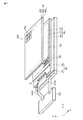
図1は、第1実施形態の液晶表示装置DSPの概略的な構成を一部分解して示す斜視図である。液晶表示装置DSPは、例えば、スマートフォン、タブレット端末、携帯電話端末、パーソナルコンピュータ、テレビ受像装置、車載装置、ゲーム機器、ウェアラブル端末等の種々の装置に用いることができる。
[First Embodiment]
FIG. 1 is a partially exploded perspective view showing a schematic configuration of the liquid crystal display device DSP of the first embodiment. The liquid crystal display device DSP can be used for various devices such as a smartphone, a tablet terminal, a mobile phone terminal, a personal computer, a television receiver, an in-vehicle device, a game machine, and a wearable terminal.
液晶表示装置DSPは、表示パネルPNLと、表示パネルPNLに平行光を照射するバックライトBLと、表示パネルPNLを透過した平行光を拡散させる拡散層STと、表示パネルPNLやバックライトBLの動作を制御する制御モジュールCMと、表示パネルPNLを駆動する駆動ICチップICと、表示パネルPNLやバックライトBLへ制御モジュールCMの制御信号を伝達するフレキシブル回路基板FPC1,FPC2と、を備えている。 The liquid crystal display device DSP includes a display panel PNL, a backlight BL that irradiates the display panel PNL with parallel light, a diffusion layer ST that diffuses the parallel light transmitted through the display panel PNL, and operations of the display panel PNL and the backlight BL. A control module CM for controlling the display, a driving IC chip IC for driving the display panel PNL, and flexible circuit boards FPC1 and FPC2 for transmitting control signals of the control module CM to the display panel PNL and the backlight BL.
本実施形態において、図1に示すように、第1方向X、第2方向Y、第3方向Zを定義する。第1方向Xは、例えば表示パネルPNLの短辺に沿う方向である。第2方向Yは、例えば表示パネルPNLの長辺に沿う方向である。第3方向Zは、第1方向X及び第2方向Yと交差する方向である。図1に示す例では、第1乃至第3方向X,Y,Zが互いに垂直に交わる。なお、第1乃至第3方向X,Y,Zが他の角度で交わってもよい。 In the present embodiment, a first direction X, a second direction Y, and a third direction Z are defined as shown in FIG. The first direction X is a direction along the short side of the display panel PNL, for example. The second direction Y is a direction along the long side of the display panel PNL, for example. The third direction Z is a direction that intersects the first direction X and the second direction Y. In the example shown in FIG. 1, the first to third directions X, Y, and Z intersect perpendicularly. The first to third directions X, Y, and Z may intersect at other angles.
表示パネル(液晶セル)PNLは、アレイ基板ARと、アレイ基板ARに対向する対向基板CTと、アレイ基板AR及び対向基板CTの間に配置された液晶層LCと、を備えている。液晶層LCは、光を選択的に透過する光学素子の一例である。表示パネルPNLは、画像を表示する表示領域DAを有している。表示パネルPNLは、表示領域DAにおいて、第1方向X及び第2方向Yにマトリクス状に配列された複数の画素PXを有している。 The display panel (liquid crystal cell) PNL includes an array substrate AR, a counter substrate CT facing the array substrate AR, and a liquid crystal layer LC disposed between the array substrate AR and the counter substrate CT. The liquid crystal layer LC is an example of an optical element that selectively transmits light. The display panel PNL has a display area DA for displaying an image. The display panel PNL includes a plurality of pixels PX arranged in a matrix in the first direction X and the second direction Y in the display area DA.
バックライトBLは、表示パネルPNLのアレイ基板ARに対向するように配置され、表示パネルPNLに背面側から偏光した平行光を照射する。バックライトBLは、光源LSと、導光部LGと、を備えている。図1に示す例では、光源LSは、アレイ基板ARの短辺に沿って配置されている。なお、光源LSは、アレイ基板ARの他の辺に沿って配置されてもよい。導光部LGは、光源LSから出射された平行光を表示パネルPNLの光学素子に向けて導光する。 The backlight BL is disposed so as to face the array substrate AR of the display panel PNL, and irradiates the display panel PNL with parallel light polarized from the back side. The backlight BL includes a light source LS and a light guide part LG. In the example shown in FIG. 1, the light source LS is arranged along the short side of the array substrate AR. The light source LS may be arranged along the other side of the array substrate AR. The light guide LG guides the parallel light emitted from the light source LS toward the optical element of the display panel PNL.
拡散層STは、バックライトBLとは反対側から表示パネルPNLに対向するように配置されている。本実施形態では、拡散層STが制御モジュールCMによって動的に駆動され、表示パネルPNLを透過した平行光の拡散/非拡散を切り替え可能に構成されている。拡散層STは、アレイ基板AR2と、アレイ基板AR2に対向する対向基板CT2と、アレイ基板AR2及び対向基板CT2の間に配置された散乱液晶層SLCと、を備えている。 The diffusion layer ST is disposed so as to face the display panel PNL from the side opposite to the backlight BL. In the present embodiment, the diffusion layer ST is dynamically driven by the control module CM, and is configured to be able to switch between diffusion / non-diffusion of parallel light transmitted through the display panel PNL. The diffusion layer ST includes an array substrate AR2, a counter substrate CT2 facing the array substrate AR2, and a scattering liquid crystal layer SLC arranged between the array substrate AR2 and the counter substrate CT2.
散乱液晶層SLCは、表示領域DAと平面視で重なり、マトリクス状に配列された複数のサブ領域PX2を有している。サブ領域PX2は、例えば平面視における面積が画素PXと同じである。ただし、サブ領域PX2の面積は、画素PXよりも大きくてもよい。この場合、サブ領域PX2を制御するための回路素子の数を減らすことができる。 The scattering liquid crystal layer SLC has a plurality of sub-regions PX2 that overlap with the display region DA in plan view and are arranged in a matrix. For example, the sub-region PX2 has the same area as the pixel PX in plan view. However, the area of the sub-region PX2 may be larger than that of the pixel PX. In this case, the number of circuit elements for controlling the sub-region PX2 can be reduced.
制御モジュールCMは、液晶表示装置DSPが搭載される電子機器のメインボード等から表示領域DAに表示するための1フレーム分の画像データを順次受信する。この画像データは、例えば各画素PXの表示色等の情報を含む。制御モジュールCMは、受信した画像データに基づいて各画素PX及び各サブ領域PX2を駆動するための信号を表示パネルPNL及び拡散層STに供給する。制御モジュールCMは、コントローラの一例である。 The control module CM sequentially receives image data for one frame to be displayed on the display area DA from a main board or the like of an electronic device on which the liquid crystal display device DSP is mounted. This image data includes information such as the display color of each pixel PX, for example. The control module CM supplies a signal for driving each pixel PX and each sub-region PX2 to the display panel PNL and the diffusion layer ST based on the received image data. The control module CM is an example of a controller.
駆動ICチップICは、例えばアレイ基板ARに実装されている。なお、駆動ICチップICは、制御モジュールCM等に実装されてもよい。フレキシブル回路基板FPC1は、アレイ基板ARと制御モジュールCMとを接続している。フレキシブル回路基板FPC2は、バックライトBLと制御モジュールCMとを接続している。 The drive IC chip IC is mounted on the array substrate AR, for example. The driving IC chip IC may be mounted on the control module CM or the like. The flexible circuit board FPC1 connects the array substrate AR and the control module CM. The flexible circuit board FPC2 connects the backlight BL and the control module CM.
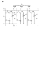
図2は、表示パネルPNLの画素PXの構成の一例を示す回路図である。図2に示す例では、画素PXは、赤色(R)、緑色(G)、青色(B)にそれぞれ対応する三つの副画素SPX(SPXR,SPXG,SPXB)を備えている。画素PXの構成はこれに限られず、例えば白色等に対応する副画素SPXをさらに備えてもよいし、同一色に対応する副画素SPXを複数備えてもよい。なお、拡散層STのサブ領域PX2は、副画素SPXと略同一の構成を備えている。そのため、代表して副画素SPXを詳しく説明し、サブ領域PX2については重複する説明を省略する。 FIG. 2 is a circuit diagram showing an example of the configuration of the pixel PX of the display panel PNL. In the example illustrated in FIG. 2, the pixel PX includes three subpixels SPX (SPXR, SPXG, SPXB) respectively corresponding to red (R), green (G), and blue (B). The configuration of the pixel PX is not limited to this. For example, the pixel PX may further include a subpixel SPX corresponding to white or the like, or may include a plurality of subpixels SPX corresponding to the same color. Note that the sub-region PX2 of the diffusion layer ST has substantially the same configuration as the sub-pixel SPX. For this reason, the subpixel SPX will be described in detail as a representative, and a duplicate description of the subregion PX2 will be omitted.
副画素SPXは、例えば薄膜トランジスタ(TFT)であるスイッチング素子SWと、画素電極PEと、をそれぞれ備えている。スイッチング素子SWは、走査信号が供給される走査線Gによって制御され、映像信号が供給される信号線S及び画素電極PEに電気的に接続されている。画素電極PEは、複数の副画素SPXに亘って配置された共通電極CEとの間で保持容量CSを形成する。画素電極PE及び共通電極CEは、例えばインジウムスズ酸化物(ITO)やインジウム亜鉛酸化物(IZO)等の透明導電材料で形成されている。 The subpixel SPX includes a switching element SW, which is a thin film transistor (TFT), for example, and a pixel electrode PE. The switching element SW is controlled by the scanning line G to which the scanning signal is supplied, and is electrically connected to the signal line S to which the video signal is supplied and the pixel electrode PE. The pixel electrode PE forms a storage capacitor CS with the common electrode CE arranged across the plurality of subpixels SPX. The pixel electrode PE and the common electrode CE are formed of a transparent conductive material such as indium tin oxide (ITO) or indium zinc oxide (IZO).
任意のスイッチング素子SWにおいて、走査線Gに走査信号が供給され、かつ信号線Sに映像信号が供給されると、映像信号に応じた電圧が画素電極PEに印加される。 In any switching element SW, when a scanning signal is supplied to the scanning line G and a video signal is supplied to the signal line S, a voltage corresponding to the video signal is applied to the pixel electrode PE.
表示パネルPNLの場合、画素電極PEと共通電極CEとの間に生じる電界によって、液晶層LCの液晶分子の配向が変化する。画素電極PEに印加する電圧を制御することによって、光源LSからの偏光を利用したカラー画像が表示領域DAに表示される。 In the case of the display panel PNL, the alignment of the liquid crystal molecules of the liquid crystal layer LC is changed by an electric field generated between the pixel electrode PE and the common electrode CE. By controlling the voltage applied to the pixel electrode PE, a color image using polarized light from the light source LS is displayed in the display area DA.
拡散層STの場合、画素電極PEと共通電極CEとの間に生じる電界によって、散乱液晶層SLCの液晶分子の配向が、電圧を印加されていない第1状態から電圧を印加された第2状態に変化する。電圧が印加されていない第1状態では、散乱液晶層SLCは、液晶分子が無秩序に配向しており光を拡散させる。電圧が印加された第2状態では、散乱液晶層SLCは、液晶分子が整列して光を透過させる。なお、拡散層STは、電圧を印加されていない場合に光を透過させ、電圧が印加された場合に光を拡散させてもよい。 In the case of the diffusion layer ST, the orientation of the liquid crystal molecules of the scattering liquid crystal layer SLC is changed from the first state where no voltage is applied to the second state where the voltage is applied, due to the electric field generated between the pixel electrode PE and the common electrode CE. To change. In the first state where no voltage is applied, the scattering liquid crystal layer SLC diffuses light because liquid crystal molecules are randomly aligned. In the second state where a voltage is applied, the scattering liquid crystal layer SLC transmits light with the liquid crystal molecules aligned. Note that the diffusion layer ST may transmit light when no voltage is applied, and may diffuse light when a voltage is applied.
各サブ領域PX2の画素電極PEに印加する電圧を制御することによって、光を拡散させる第1状態(拡散状態)と、光を透過させる第2状態(非拡散状態)との間で、散乱液晶層SLCの状態をサブ領域PX2単位で動的に切り替えることができる。このような散乱液晶層SLCとして、例えば高分子ネットワーク型液晶(Polymer Network Liquid Crystal)や高分子分散型液晶(Polymer Dispersed Liquid Crystal)等が挙げられる。散乱液晶層SLCに関する公知技術として、例えば特開2009−210725号公報及び特開2006―3392号公報が挙げられる。 By controlling the voltage applied to the pixel electrode PE of each sub-region PX2, the liquid crystal is scattered between the first state (diffused state) in which light is diffused and the second state (non-diffused state) in which light is transmitted. The state of the layer SLC can be dynamically switched in units of subregions PX2. Examples of such a scattering liquid crystal layer SLC include a polymer network type liquid crystal (Polymer Network Liquid Crystal) and a polymer dispersion type liquid crystal (Polymer Dispersed Liquid Crystal). Examples of known techniques related to the scattering liquid crystal layer SLC include Japanese Unexamined Patent Application Publication Nos. 2009-210725 and 2006-3392.
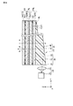
図3は、液晶表示装置DSPを示す断面図である。表示パネルPNLのアレイ基板AR及び対向基板CTは、透光性を有した第1基板11及び第2基板12をそれぞれ備えている。同様に、拡散層STのアレイ基板AR2及び対向基板CT2は、透光性を有した第3基板13及び第4基板14をそれぞれ備えている。
FIG. 3 is a cross-sectional view showing the liquid crystal display device DSP. The array substrate AR and the counter substrate CT of the display panel PNL include a
本実施形態では、第1乃至第4基板11,12,13,14は、ガラス基板からそれぞれ形成されている。なお、第1乃至第4基板11,12,13,14をアクリル樹脂等の透光性の樹脂材料から形成してもよい。
In the present embodiment, the first to
第1基板11は、第1面F1と、第1面F1とは反対側の第2面F2と、を有している。第2基板12は、第3面F3と、第3面F3とは反対側の第4面F4と、を有している。第3基板13は、第5面F5と、第5面F5とは反対側の第6面F6と、を有している。第4基板14は、第7面F7と、第7面F7とは反対側の第8面F8と、を有している。これら第1乃至第8面F1〜F8は、例えば第1方向X及び第2方向Yと平行な面である。
The
表示パネルPNLのアレイ基板ARと対向基板CTとは、第1面F1と第3面F3とを対向させた状態で、シール材SLによって貼り合わされている。シール材SLは、表示領域DAを囲む環状に形成されている。アレイ基板AR、対向基板CT及びシール材SLによって囲まれた空間に液晶層LCが封入されている。 The array substrate AR and the counter substrate CT of the display panel PNL are bonded to each other with the seal material SL in a state where the first surface F1 and the third surface F3 are opposed to each other. The sealing material SL is formed in an annular shape surrounding the display area DA. A liquid crystal layer LC is sealed in a space surrounded by the array substrate AR, the counter substrate CT, and the sealing material SL.
同様に、拡散層STのアレイ基板AR2と対向基板CT2とは、第5面F5と第7面F7とを対向させた状態で、シール材SL2によって縁部を環状に貼り合わされ、散乱液晶層SLCを封入されている。 Similarly, the array substrate AR2 and the counter substrate CT2 of the diffusion layer ST are bonded to each other in a ring shape by the sealing material SL2 with the fifth surface F5 and the seventh surface F7 facing each other, and the scattering liquid crystal layer SLC. Is enclosed.
表示パネルPNLの対向基板CTと、拡散層STのアレイ基板AR2とは、第4面F4と第6面F6とを対向させた状態で配置されている。表示パネルPNLと拡散層STとの間には、偏光板PLが配置されている。図3に示す例では、偏光板PLは、第2基板12の第4面F4に貼着されている。本開示において、各実施形態の液晶表示装置DSPは、第1基板11と光源LSの間や、第1基板11と液晶層LCの間に背面側の偏光板が配置されていない。
The counter substrate CT of the display panel PNL and the array substrate AR2 of the diffusion layer ST are arranged with the fourth surface F4 and the sixth surface F6 facing each other. A polarizing plate PL is disposed between the display panel PNL and the diffusion layer ST. In the example illustrated in FIG. 3, the polarizing plate PL is attached to the fourth surface F4 of the
光源LSは、偏光板PLの吸収軸と平行な方向に振動する偏光した光を照射する発光素子21と、レンズ22と、を備えている。発光素子21は、導光部LGに対向している。レンズ22は、発光素子21と導光部LGとの間に配置される。
The light source LS includes a
本実施形態では、発光素子21は、第2方向Yを中心とした広がりを持つ発散光を照射する点光源である。このような発光素子21としては、例えば偏光したレーザ光を放つ半導体レーザ等のレーザ素子を用いることができる。レンズ22は、発光素子21からの光を平行光に変換し、導光部LGに照射する。このようなレンズ22としては、例えばフレネルレンズや回折レンズ等を用いることができる。
In the present embodiment, the
光源LSは、点光源である複数の発光素子21とレンズ22とから平行光を作り出す。なお、光源LSは、例えば第1方向Xに長尺な線状の発光面を有した発光素子を備えてもよい。また、発光素子21は前述したレーザ光を放つものに限られず、例えば偏光した光を放つ発光ダイオードを用いることもできる。平行光は、コリメート光とも呼ばれ、空間を実質的に一直線に進む光であって高い指向性を有している。本明細書において、平行光は、光線が厳密に平行である光に限定されるものではなく、僅かに広がりを持った実質的に平行な光を含む。
The light source LS generates parallel light from a plurality of
導光部LGは、レンズ22で集光された平行光を液晶層LCに向けて導光する。本実施形態の導光部LGは、導光板30と、導光板30に設けられた光指向部40とで構成されている。導光板30は、例えば透光性を有する樹脂材料から形成された板状の部材である。導光板30は、表示パネルPNLの背面側に配置され、第1基板11と対向している。なお、後で詳しく述べるが、導光部LGの構成はこれに限られず、アレイ基板AR等の一部を導光部LGの一部として構成することもできる。
The light guide LG guides the parallel light collected by the
液晶表示装置DSPは、表示パネルPNL、バックライトBL、拡散層ST等に加え、フレームFRをさらに備えている。フレームFRは、バックベゼル51と、フロントベゼル52と、を備えている。バックベゼル51は、支持部の一例であり、少なくとも一部が透光性を有している。
The liquid crystal display device DSP further includes a frame FR in addition to the display panel PNL, the backlight BL, the diffusion layer ST, and the like. The frame FR includes a
図3に示す例では、バックベゼル51は、表示パネルPNLの背面及び側面と、光源LSとを覆っている。バックベゼル51は、表示領域DAと平面視で重なる透光部51Aが透明に形成されている。なお、透明な透光部51Aを形成する代わりに、透光部51Aの位置に開口を形成してバックベゼル51に透光性を確保してもよい。
In the example illustrated in FIG. 3, the
フロントベゼル52は、表示領域DAに対応した開口52Aを有し、光源LS及び表示パネルPNLの前面側の周縁を覆っている。
The front bezel 52 has an
導光板30、表示パネルPNL、偏光板PL、拡散層STは、バックベゼル51及びフロントベゼル52によって挟持されている。発光素子21及びレンズ22は、バックベゼル51及びフロントベゼル52の間に形成された空間に配置され、例えばバックベゼル51に固定されている。
The
図4は、本実施形態に係る表示パネルPNLの構成の一例を拡大して示す断面図である。図4に示す例は、副画素SPXR,SPXG,SPXBに対応する概略的な構造であり、アレイ基板ARに形成される走査線G、信号線S、スイッチング素子SW等を省略している。 FIG. 4 is an enlarged cross-sectional view showing an example of the configuration of the display panel PNL according to the present embodiment. The example shown in FIG. 4 is a schematic structure corresponding to the subpixels SPXR, SPXG, and SPXB, and the scanning lines G, signal lines S, switching elements SW, and the like formed on the array substrate AR are omitted.
アレイ基板ARは、第1基板11に加え、絶縁層ILと、第1配向膜AL1と、前述の画素電極PEと、を備えている。絶縁層ILは、第1基板11の第1面F1に形成されている。画素電極PEは、絶縁層ILの対向基板CT側の面に形成されている。第1配向膜AL1は、絶縁層IL及び画素電極PEを覆っている。
In addition to the
対向基板CTは、第2基板12に加え、遮光層BMと、カラーフィルタCFと、オーバーコート層OCと、前述の共通電極CEと、第2配向膜AL2と、を備えている。
In addition to the
遮光層BMは、第2基板12の第3面F3に形成されており、副画素SPXを区画している。カラーフィルタCFは、第3面F3及び遮光層BMを覆っている。オーバーコート層OCは、カラーフィルタCFを覆っている。オーバーコート層OCによって遮光層BMやカラーフィルタCFにより生じる凹凸が平坦化される。共通電極CEは、オーバーコート層OCのアレイ基板AR側の面に形成されている。第2配向膜AL2は、共通電極CEを覆っている。
The light shielding layer BM is formed on the third surface F3 of the
第1配向膜AL1と第2配向膜AL2との間に液晶層LCが封入されている。なお、図4に示す例では、画素電極PEと共通電極CEとの間に第3方向Zと平行な電界が発生し、この電極を用いて液晶層LCの液晶分子の配向状態を選択的に変化させる構成を示している。しかしながら、表示パネルPNLは、第1方向X及び第2方向Yと平行な電界によって液晶層LCの液晶分子の配向状態を選択的に変化させる構成を有していてもよい。この場合、共通電極CEは、アレイ基板ARの画素電極PEと同じ層に配置してもよいし、アレイ基板ARの画素電極PEとは異なる層に配置してもよい。 A liquid crystal layer LC is sealed between the first alignment film AL1 and the second alignment film AL2. In the example shown in FIG. 4, an electric field parallel to the third direction Z is generated between the pixel electrode PE and the common electrode CE, and the alignment state of the liquid crystal molecules of the liquid crystal layer LC is selectively used by using this electrode. The structure to change is shown. However, the display panel PNL may have a configuration in which the alignment state of the liquid crystal molecules in the liquid crystal layer LC is selectively changed by an electric field parallel to the first direction X and the second direction Y. In this case, the common electrode CE may be arranged in the same layer as the pixel electrode PE of the array substrate AR, or may be arranged in a different layer from the pixel electrode PE of the array substrate AR.
カラーフィルタCFは、赤色に対応するカラーフィルタCFRと、緑色に対応するカラーフィルタCFGと、青色に対応するカラーフィルタCFBとを含んでいる。カラーフィルタCFRは副画素SPXRに配置され、カラーフィルタCFGは副画素SPXGに配置され、カラーフィルタCFBは副画素SPXBに配置されている。 The color filter CF includes a color filter CFR corresponding to red, a color filter CFG corresponding to green, and a color filter CFB corresponding to blue. The color filter CFR is disposed in the subpixel SPXR, the color filter CFG is disposed in the subpixel SPXG, and the color filter CFB is disposed in the subpixel SPXB.
なお、画素PXが白色に対応する副画素SPXを備える場合、この副画素SPXは白色に対応する透明なカラーフィルタを備えてもよいし、カラーフィルタを備えなくてもよい。また、カラーフィルタCF(CFR,CFG,CFB)を偏光板PLと拡散層STとの間やアレイ基板ARに設けることもできる。 In addition, when the pixel PX includes a sub-pixel SPX corresponding to white, the sub-pixel SPX may include a transparent color filter corresponding to white, or may not include a color filter. Further, a color filter CF (CFR, CFG, CFB) can be provided between the polarizing plate PL and the diffusion layer ST or on the array substrate AR.
光源LSからの平行光は、導光部LGに導光されてアレイ基板AR、液晶層LC、対向基板CTを通過する。この平行光は、カラーフィルタCFに対応する色の可視光となって偏光板PLに到達する。画素電極PEと共通電極CEとの間に電界が形成された副画素SPXを通過した平行光は、吸収されることなく偏光板PLを透過し、拡散層STで拡散される。平行光が拡散されることで、表示領域DAに表示される画像の視野角特性を改善することができる。 The parallel light from the light source LS is guided to the light guide LG and passes through the array substrate AR, the liquid crystal layer LC, and the counter substrate CT. The parallel light reaches the polarizing plate PL as visible light having a color corresponding to the color filter CF. The parallel light that has passed through the sub-pixel SPX in which an electric field is formed between the pixel electrode PE and the common electrode CE passes through the polarizing plate PL without being absorbed and is diffused by the diffusion layer ST. By diffusing the parallel light, the viewing angle characteristics of the image displayed in the display area DA can be improved.
図5乃至図8は、光源LS及び導光板30の具体例である。図5に示すように、光源LSは、複数組の発光素子21及びレンズ22を備えている。各組の発光素子21及びレンズ22は、第1方向Xに沿って並んでいる。各発光素子21は、例えば前述のフレキシブル回路基板FPC2と電気的に接続された配線基板に実装されている。なお、光源LSは、発光素子21及びレンズ22を一組のみ備えるものであってもよい。
5 to 8 are specific examples of the light source LS and the
導光板30は、その内部を通過する偏光した平行光の偏光方向を維持する観点から、低複屈折性を有することが好ましい。例えば、導光板30のリタデーションは、入射される平行光の主波長の四分の一以下であることが好ましい。導光板30は、例えば正の複屈折物質と負の複屈折物質との混合体又は共重合体からなる固有複屈折率が絶対値で3×10⁻³以下のポリマー等で形成されている。
The
混合体は、固有複屈折率が正のポリマーと負のポリマーとが適切な比率で混合されることにより、ポリマーに配向が生じたときに互いに複屈折が相殺しあい、巨視的に複屈折を発現させない。或いは、混合体は、棒状の分子形状と分極率の異方性とを有する低分子をポリマーに添加することにより、ポリマーの複屈折を相殺する。共重合体は、固有複屈折率が正のモノマーと負のモノマーとを適切な比率で共重合させ、一つのポリマー鎖内で異方性を相殺する。このようなポリマーとして、例えば特許第5263771号公報の(0043)段落〜(0052)段落に記載のものを適用することができる。 In the mixture, a polymer with a positive intrinsic birefringence and a negative polymer are mixed in an appropriate ratio, so that when the polymer is oriented, the birefringence cancels each other, and the birefringence appears macroscopically. I won't let you. Alternatively, the mixture offsets the birefringence of the polymer by adding small molecules having a rod-like molecular shape and polarizability anisotropy to the polymer. In the copolymer, a monomer having a positive intrinsic birefringence and a negative monomer are copolymerized at an appropriate ratio, and anisotropy is offset within one polymer chain. As such a polymer, for example, those described in paragraphs (0043) to (0052) of Japanese Patent No. 5263377 can be applied.
導光板30は、側面31と、第1主面32と、第2主面33と、を有している。側面31は、光源LSに対向し、第1主面32は、表示パネルPNLに対向し、第2主面33は、第1主面32とは反対側に位置している。
The
側面31は、XZ平面から傾斜しており、例えば第1主面32と鈍角をなすとともに第2主面33と鋭角をなす。光源LSから出射した平行光は、側面31を通って導光板30の内部に入射する際、平行性を維持したまま第2主面33に向かって屈折する。第2主面33には、光指向部40が形成されている。なお、側面31、第1主面32、第2主面33を入射面、出射面、反射面とそれぞれ呼ぶこともできる。
The
図6は、光指向部40を拡大して示す断面図である。図6に示すように、光指向部40は、光源LSの方向を向いた傾斜面41と、光源LSの反対方向を向いた傾斜面42と、傾斜面41,42の第2主面33側の端部を繋ぐ平坦面43と、を有している。
FIG. 6 is an enlarged cross-sectional view of the
傾斜面41,42は、第1基板11の第1面F1や第2面F2に対して傾いている。傾斜面41,42は、第1方向Xと平行に延び、第2方向Y及び第3方向Zと交わる平面である。光源LSを臨む傾斜面41は、側面31から第2主面33へ向かう平行光を鏡面反射して第1主面32に光路を指向させる。
The inclined surfaces 41 and 42 are inclined with respect to the first surface F1 and the second surface F2 of the
図6に示す例では、平坦面43は、第1方向X及び第2方向Yと平行であり、第1主面32と対向する平面である。平坦面43は、バックベゼル51に面接触している。平坦面43とバックベゼル51とが面接触すれば、バックベゼル51によって表示パネルPNLを安定して支持することができる。第1主面32と平行な平坦面43は、第1主面32に垂直な光を屈折させない。表示パネルPNLの厚さ方向(第3方向Z)の光を効率的に透過して液晶表示装置DSPの光の透過率を向上させることができる。
In the example shown in FIG. 6, the
なお、光指向部40の形状は図6に示した形状に限られない。例えば、図7に示すように、傾斜面41,42の第1主面32側の端部を繋ぎ、第1主面32に平行な平坦面44をさらに有していてもよい。この場合、平坦面43に加えて平坦面44でも光を効率的に透過できるため、液晶表示装置DSPの光の透過率が向上する。光指向部40は、レンズ22と傾斜面41,42とが等距離になる扇形に形成してもよい。この場合、傾斜面41,42は曲面である。
The shape of the
導光板30の厚さは均一である必要はなく、少なくとも一部において異なっていてもよい。一例として、図8に示すように光源LSに近づくに従い光指向部40と第1基板11との距離が大きくなる楔形に導光板30を形成してもよい。光指向部40は、光源LSの方向を向いた傾斜面41と、第1方向X及び第2方向Yと平行な平坦面45とが交互に配置されている。この場合、光指向部40が側面31に向かって傾斜されるため、側面31が光指向部40に向かって傾斜されていなくても、光源LSからの平行光を光指向部40へ指向させることができる。
The thickness of the
表示領域DAに垂直に投影された傾斜面(41,42)の面積の総和よりも平坦面(43,44,45)の面積の総和が大きくなるように光指向部40を形成すれば、液晶表示装置DSPの光の透過率を好適に高めることができる。一方、平坦面が占める比率を極端に大きくすると、第1主面32から出射する光源LSからの平行光に輝度ムラが生じる場合がある。傾斜面と平坦面との比率は、液晶表示装置DSPに求められる性能に応じて適宜調整できる。
If the
以上のように構成された本実施形態の液晶表示装置DSPは、表示領域DAと平面視で重なる透光部51Aが透明に形成されたバックベゼル51を備えている。そのため、表示領域DAに表示された画像を視認できると同時に、液晶表示装置DSPの背面側に配置された背景物を透過して視認できる。
The liquid crystal display device DSP of the present embodiment configured as described above includes a
本実施形態の光源LSは、偏光した平行光を照射する。一般的な液晶表示装置では表示パネルの両側にそれぞれ偏光板を配置する必要があるが、本実施形態では、前面側の偏光板PLのみを配置すればよい。偏光板が二枚あると、偏光板を通過する毎に50%ずつ減少して25%しか光が透過されない。本実施形態では、偏光板の数を二枚から一枚に減らしたことにより、偏光板に起因した光のロスを低減できる。その結果、液晶表示装置DSPの光の透過率を向上させ、背面側に配置された背景物を透過して良好に視認できる。しかも、偏光板の数が減った分、液晶表示装置DSPを薄型化することもできる。 The light source LS of this embodiment irradiates polarized parallel light. In a general liquid crystal display device, it is necessary to dispose polarizing plates on both sides of the display panel, but in this embodiment, only the polarizing plate PL on the front side may be disposed. When there are two polarizing plates, each time the light passes through the polarizing plate, it decreases by 50% and only 25% is transmitted. In the present embodiment, by reducing the number of polarizing plates from two to one, it is possible to reduce light loss due to the polarizing plates. As a result, the light transmittance of the liquid crystal display device DSP can be improved, and the background object arranged on the back side can be transmitted and visually recognized. In addition, the liquid crystal display device DSP can be made thinner as the number of polarizing plates is reduced.
液晶表示装置DSPの光の透過率が低い場合、背景物の視認性を向上させるために光源の強度を高めなければならない。例えば、小売店の冷蔵庫のガラス扉を透明表示装置として構成した場合、炭酸飲料等の背景物を透過させるために光源の強度を高めると、発熱量が大きくなって低温を保持することが困難になる。本実施形態であれば、偏光板の数を減らして光の透過率を向上させているため、光源の強度を高めることなく背景物を良好に視認できる。そのため、発熱量を大きくできない環境の表示装置に適用することができる。また、液晶表示装置DSPの電力消費を節約できる。 When the light transmittance of the liquid crystal display device DSP is low, the intensity of the light source must be increased in order to improve the visibility of the background. For example, when the glass door of a refrigerator in a retail store is configured as a transparent display device, if the intensity of the light source is increased in order to allow background materials such as carbonated drinks to pass therethrough, the amount of heat generation increases and it is difficult to maintain a low temperature. Become. According to this embodiment, since the light transmittance is improved by reducing the number of polarizing plates, the background can be visually recognized without increasing the intensity of the light source. Therefore, the present invention can be applied to a display device in an environment where the heat generation amount cannot be increased. Further, power consumption of the liquid crystal display device DSP can be saved.
例えば、図8の通り、本実施形態の光源LSは、平行光を照射する。低複屈折性を有する導光板30の内部であっても、反射を繰り返して光路が長くなると光の偏光度を維持することが困難になるため、光の反射回数を減らすことが望ましい。光源LSが照射する光が平行光であれば、光指向部40に向かう角度を制御し易い。最低限の反射回数で光指向部40に平行光を入射させ、偏光度を維持したまま第2基板12に向かって平行光を指向させることができる。さらに、反射回数が少ないと光路長も短くなる。導光板30の内部における光の吸収を低減し、液晶表示装置DSPの光の透過率をより一層高めることができる。
For example, as shown in FIG. 8, the light source LS of the present embodiment emits parallel light. Even within the
本実施形態の液晶表示装置DSPは、第2基板12の第4面F4側に配置された拡散層STを備えている。偏光板PLを通過直後の光は平行光であるため、視野角が狭く正面以外から画像を視認しづらい。拡散層STによって光が拡散されることで、表示領域DAに表示される画像の視野角特性を改善することができる。
The liquid crystal display device DSP of this embodiment includes a diffusion layer ST disposed on the fourth surface F4 side of the
本実施形態の拡散層STは、光を拡散させる第1状態と光を透過させる第2状態との間で状態が動的に切り替わる散乱液晶層SLCを含んでいる。そのため、拡散層STで光を拡散させて画像の視野角特性を改善したいタイミングと、拡散層STで光を拡散させないで背景物の視認性を高めたいタイミングとを任意に切り替えることができる。 The diffusion layer ST of the present embodiment includes a scattering liquid crystal layer SLC whose state is dynamically switched between a first state in which light is diffused and a second state in which light is transmitted. Therefore, it is possible to arbitrarily switch the timing at which light is diffused by the diffusion layer ST to improve the viewing angle characteristics of the image and the timing at which the visibility of the background object is to be improved without diffusing light by the diffusion layer ST.
本実施形態の拡散層STは、図1の通り、表示領域DAと平面視で重なり、マトリクス状に配列された複数のサブ領域PX2を有している。液晶表示装置DSPは、制御モジュールCMによって任意のサブ領域PX2において散乱液晶層SLCの状態を切り替えることができる。 As shown in FIG. 1, the diffusion layer ST of the present embodiment has a plurality of sub-regions PX2 that overlap with the display region DA in plan view and are arranged in a matrix. The liquid crystal display device DSP can switch the state of the scattering liquid crystal layer SLC in an arbitrary sub-region PX2 by the control module CM.
例えば、表示領域DAの中央部において拡散層STに光を拡散させ、周縁部において拡散層STに光を透過させれば、中央部に表示された画像の視野角特性を改善させると同時に、周縁部において背景物を良好に視認させることができる。 For example, if the light is diffused in the diffusion layer ST in the central portion of the display area DA and the light is transmitted through the diffusion layer ST in the peripheral portion, the viewing angle characteristic of the image displayed in the central portion is improved and the peripheral edge is improved. The background can be seen well at the part.
さらに、制御モジュールCMは、表示領域DAに表示される画像に応じてサブ領域PX2の状態を切り替えることもできる。例えば、制御モジュールCMは、表示領域DAに含まれる第1領域と対向するサブ領域PX2を第1状態に設定し、第1領域とは異なる第2領域と対向するサブ領域PX2を第2状態に設定してもよい。この場合、第1領域において画像の視認性が高まり、第2領域において背景物の視認性が高まる。 Furthermore, the control module CM can also switch the state of the sub area PX2 according to the image displayed in the display area DA. For example, the control module CM sets the sub area PX2 facing the first area included in the display area DA to the first state, and sets the sub area PX2 facing the second area different from the first area to the second state. It may be set. In this case, the visibility of the image is enhanced in the first area, and the visibility of the background object is enhanced in the second area.
第1領域は、例えば文字列や絵柄等の観察者に伝達すべき情報を表す特定画像が表示される領域であり、第2領域は、上記特定画像の背景に相当する領域である。第1領域と第2領域とを区別するための情報は、制御モジュールCMが外部から受信する画像データに含まれてもよい。或いは、制御モジュールCMが外部から受信する画像を解析することにより、第1領域と第2領域とを判別してもよい。
その他、本実施形態からは、種々の好適な効果を得ることができる。
The first area is an area where a specific image representing information to be transmitted to an observer such as a character string or a picture is displayed, and the second area is an area corresponding to the background of the specific image. Information for distinguishing between the first area and the second area may be included in the image data received from the outside by the control module CM. Or you may discriminate | determine a 1st area | region and a 2nd area | region by analyzing the image which control module CM receives from the outside.
In addition, various suitable effects can be obtained from this embodiment.
[第2実施形態]
第1実施形態では、導光板30を備えた導光部LGの構成を開示した。第2実施形態では、図9及び図10を参照して導光板30を備えていない導光部LGの構成を説明する。図9に示すように、第2実施形態の液晶表示装置DSPは、プリズムシート46を備えている。プリズムシート46は、例えば図3に示したバックベゼル51に貼着される。プリズムシート46は、光源LSから出射した平行光の光路を第2基板12に向けて指向させる光指向部の一例である。
[Second Embodiment]
In 1st Embodiment, the structure of the light guide part LG provided with the light-
プリズムシート46と表示パネルPNLとの間は、導光板30が配置されていない空隙である。光源LSから出射された平行光は、導光板30の側面(入射面)31を経由せずプリズムシート46へ直に入射する。
A space between the
なお、プリズムシート46は、図10に示す変形例のように、バックベゼル51ではなく、アレイ基板ARの第2面F2に貼着することもできる。図10に示す構成でも、光源LSから出射された平行光は、導光板30の側面31を経由せずプリズムシート46へ直に入射する。
Note that the
図9及び図10に示すプリズムシート46は、第1実施形態における導光板30の光指向部40と同様に、光源LSの方向を向いた傾斜面47と、光源LSの反対方向を向いた傾斜面48と、傾斜面47,48の第2主面33側の端部を繋ぐ平坦面49と、を有している。なお、プリズムシートは、傾斜面47,48の第1主面32側の端部を繋ぐ平坦面さらに有していてもよい。光源LSに向かって傾斜させ、傾斜面と平坦面とを交互に配置してもよい。
The
第2実施形態及びその変形例によれば、第1実施形態と同様に偏光板PLが一枚であるため、液晶表示装置DSPの光の透過率を向上させることができる。さらに、導光板30を省略できるため、導光板30における偏光度の低下や光学特性の低下を抑制して画像の表示品位を向上させることができる。液晶表示装置DSPの光の透過率をより一層高め、背景物を良好に視認できる。
According to the second embodiment and its modification, since the number of polarizing plates PL is one as in the first embodiment, the light transmittance of the liquid crystal display device DSP can be improved. Furthermore, since the
[第3実施形態]
第3実施形態について、図11を参照して説明する。第3実施形態では、光源LSから出射された平行光は、導光板30の側面31ではなく、アレイ基板ARの側面F9に入射する。つまり、第3実施形態では、アレイ基板ARが導光部LGの一部として機能する。
[Third Embodiment]
A third embodiment will be described with reference to FIG. In the third embodiment, the parallel light emitted from the light source LS enters the side surface F9 of the array substrate AR, not the
図11の例において、第1基板11の第2面F2にプリズムシート46が貼着されている。プリズムシート46の形状は、第2実施形態と同様である。光源LSから側面F9に入射した平行光は、アレイ基板ARに貼着されたプリズムシート46に入射し、第2基板12に向かって指向される。
In the example of FIG. 11, a
第3実施形態によれば、第1及び第2実施形態と同様に偏光板PLが一枚であるため、液晶表示装置DSPの光の透過率を向上させることができる。導光板30を省略できるため、導光板30における偏光度の低下や光学特性の低下を抑制して画像の表示品位を向上させることもできる。さらに、第3実施形態では、光源LSから出射された平行光の光路をアレイ基板ARの内部に取り込んでいるため、平行光の光路として導光板30や空隙を設ける必要がない。これにより、液晶表示装置DSPを薄型化することができる。
According to the third embodiment, since the number of polarizing plates PL is one as in the first and second embodiments, the light transmittance of the liquid crystal display device DSP can be improved. Since the
[第4実施形態]
第4実施形態について、図10と図12乃至図14とを参照して説明する。第4実施形態の液晶表示装置DSPは、図10に示す第2実施形態の変形例の液晶表示装置DSPと略同一の構成を備えている。ただし、第4実施形態の液晶表示装置DSPは、光源LSに代えて、図12に示すように第1色の光を点灯させる第1光源LS1と、第1色とは異なる第2色の光を点灯させる第2光源LS2と、第1色及び第2色とは異なる第3色の光を点灯させる第3光源LS3と、を備えている。例えば、第1色は赤色、第2色は緑色、第3色は青色である。第1乃至第3光源LS1,LS2,LS3から出射される光は、すべて偏光した平行光である。
[Fourth Embodiment]
A fourth embodiment will be described with reference to FIG. 10 and FIGS. 12 to 14. The liquid crystal display device DSP of the fourth embodiment has substantially the same configuration as the liquid crystal display device DSP of the modification of the second embodiment shown in FIG. However, in the liquid crystal display device DSP of the fourth embodiment, instead of the light source LS, as shown in FIG. 12, the first light source LS1 that turns on the first color light, and the second color light different from the first color. And a third light source LS3 that lights light of a third color different from the first color and the second color. For example, the first color is red, the second color is green, and the third color is blue. The light emitted from the first to third light sources LS1, LS2, LS3 is all polarized parallel light.
第4実施形態では、第1乃至第3光源LS1,LS2,LS3を時分割で高速点灯させるとともに、これに同期して画像を高速で切り替え、各色を時分割で混合する。第1乃至第3光源LS1,LS2,LS3から出射された光は、第1基板11の第2面F2に貼着されたプリズムシート46に入射する。プリズムシート46に入射した光は、液晶層LCを通過する。
In the fourth embodiment, the first to third light sources LS1, LS2, and LS3 are turned on at high speed in a time division manner, and the images are switched at a high speed in synchronization with this to mix the colors in a time division manner. Light emitted from the first to third light sources LS1, LS2, and LS3 is incident on the
第4実施形態の液晶表示装置DSPでは、液晶層LCを通過する光がすでに赤色、緑色、青色に着色されているため、カラーフィルタCFを省略することができる。そのため、液晶表示装置DSPの光の透過率をより一層向上させることができる。 In the liquid crystal display device DSP of the fourth embodiment, since the light passing through the liquid crystal layer LC is already colored in red, green, and blue, the color filter CF can be omitted. Therefore, the light transmittance of the liquid crystal display device DSP can be further improved.
[第5実施形態]
第5実施形態について、図13を参照して説明する。第5実施形態の液晶表示装置DSPは、第2基板12に設けられた発光層60を備えている。
[Fifth Embodiment]
A fifth embodiment will be described with reference to FIG. The liquid crystal display device DSP of the fifth embodiment includes a
第5実施形態では、発光素子21が放つ光は励起光である。励起光は、例えば主波長が420nm未満のレーザ光(紫外光)や420nm以上480nm未満のレーザ光(青色光)である。発光層60は、透光性を有した透明基材61と、蛍光体層62と、を備えている。透明基材61は、偏光板PLに貼着されている。蛍光体層62は、透明基材61の一面に配置されている。具体的には、副画素SPXR,SPXG,SPXBには、励起光を吸収して赤色、緑色、青色にそれぞれ発光する蛍光体層62,62GR,62Bが配置されている。なお、励起光が青色光である場合、蛍光体層62Bを省略してもよい。
In the fifth embodiment, the light emitted from the
蛍光体層62R,62G,62Bは、それぞれ第1乃至第3蛍光体63R,63G,63Bを含んでいる。第1乃至第3蛍光体63R,63G,63Bとして、例えば、光源LSからの光を受けて赤色、緑色、青色にそれぞれ発光する量子ドットを用いることができる。量子ドットは、例えば半導体の微粒子であり、粒径を調整することによって種々の波長の光を発生させることができる。
The phosphor layers 62R, 62G, and 62B include first to
図13に示す例では、互い隣接する副画素SPXの境界にバンク64が配置されている。バンク64は、例えば遮光性を有する黒色樹脂から形成されており、互いに隣接する一方の副画素SPXからの発光が他方の副画素SPXに入射することを防止する。なお、発光層60は、バンク64を備えていなくてもよい。この場合、開口率が増加して液晶表示装置DSPの光の透過率が向上する。
In the example shown in FIG. 13, the
図13に示す例では、発光層60の上に拡散層ST2が配置されている。拡散層ST2は、例えば、散乱粒子が分散された樹脂フィルムである。散乱粒子に代えて、表面に微細なレンズ構造を形成してもよい。散乱粒子は、光を散乱させるものであれば特に限定されず、有機粒子であっても無機粒子であってもよい。有機粒子として、例えばアクリル樹脂、シリコン樹脂、スチレン樹脂等の樹脂粒子が挙げられる。無機粒子として、例えば、シリカ、アルミナ等のセラミック粒子や、アルミニウム、銅、鉄等の金属粒子が挙げられる。散乱液晶層を含む拡散層STだけでなく、このように構成された拡散層ST2によっても、画像の輝度ムラを低減し、視野角特性を改善することができる。
In the example shown in FIG. 13, the diffusion layer ST <b> 2 is disposed on the
第5実施形態の構成によれば、発光層60が、励起光を吸収して可視光波長域の光を発光する。光源LSからの平行光の利用効率が高いため、液晶表示装置DSPの消費電力を低減することができる。しかも、発光層60は、第1乃至第3蛍光体63R,63G,63Bを含有している。第1乃至第3蛍光体63R,63G,63Bが励起光を吸収して三原色波長域の光をそれぞれ発光するため、カラーフィルタCFを省略できる。加えて、第5実施形態では、光源LSからの平行光が励起光である。励起光であれば、主波長が肉眼で視認されづらいため、発光層60で吸収されずに表示領域DAに漏れたとしても、液晶表示装置DSPの表示品位を低下させづらい。
According to the configuration of the fifth embodiment, the
本発明のいくつかの実施形態を説明したが、これらの実施形態は、例として提示したものであり、発明の範囲を限定することは意図していない。これら新規な実施形態は、その他の様々な形態で実施されることが可能であり、発明の要旨を逸脱しない範囲で、種々の省略、置き換え、変更を行うことができる。これら実施形態やその変形例は、発明の範囲や要旨に含まれるとともに、特許請求の範囲に記載された発明とその均等の範囲に含まれる。各実施形態にて開示した構成は、適宜に組み合わせることができる。 Although several embodiments of the present invention have been described, these embodiments are presented by way of example and are not intended to limit the scope of the invention. These novel embodiments can be implemented in various other forms, and various omissions, replacements, and changes can be made without departing from the scope of the invention. These embodiments and modifications thereof are included in the scope and gist of the invention, and are included in the invention described in the claims and equivalents thereof. The configurations disclosed in the embodiments can be combined as appropriate.
例えば、第1乃至第4実施形態において、散乱液晶層SLCにより第1状態と第2状態との間で状態を動的に切り替え可能な拡散層STに代えて、第5実施形態で説明した拡散層ST2を適用してもよい。或いは、平行光の偏光度を解消しない拡散粘着層を適用してもよい。拡散粘着層は、第2基板12の第4面F4と偏光板PLとの間に配置され、第4面F4に偏光板PLを貼着する。或いは、第5実施形態において、拡散層ST2に代えて、蛍光体層62(62R,62G,62B)が散乱粒子を含むように構成してもよい。第1状態と第2状態との間で状態を動的に切り替え可能な拡散層STを適用してもよい。
For example, in the first to fourth embodiments, the diffusion described in the fifth embodiment instead of the diffusion layer ST that can be dynamically switched between the first state and the second state by the scattering liquid crystal layer SLC. The layer ST2 may be applied. Alternatively, a diffusion adhesive layer that does not eliminate the degree of polarization of parallel light may be applied. The diffusion adhesive layer is disposed between the fourth surface F4 of the
11…第1基板、12…第2基板、40,46…光指向部、43,44,45,48…平坦面、51…バックベゼル(支持部の一例)、60…発光層、63R…第1蛍光体、63G…第2蛍光体、CM…制御モジュール(コントローラの一例)、DA…表示領域、DSP…液晶表示装置、F1…第1面、F2…第2面、F3…第3面、F4…第4面、F9…側面、FR…フレーム、LC…液晶層、LS…光源、PL…偏光板(偏光素子の一例)、PNL…表示パネル、PX2…サブ領域、SLC…散乱液晶層、ST,ST2…拡散層。
DESCRIPTION OF
Claims (10)
前記第1基板の前記第1面に対向する第3面と、前記第3面の反対側の第4面と、を有する透光性の第2基板と、
前記第1基板と前記第2基板との間に配置された液晶層と、
前記第2基板の前記第4面側に配置された偏光素子と、
偏光した平行光を照射する光源と、
前記第1基板の前記第2面側に配置され、前記光源から出射した前記平行光の光路を、前記第2基板に向けて指向させる光指向部と、
前記第1基板、前記第2基板、前記光源及び前記光指向部を支持するフレームと、を備え、
前記フレームは、前記光指向部に面する支持部を有し、
前記支持部は、透光性を有している、表示装置。 A translucent first substrate having a first surface and a second surface opposite to the first surface;
A translucent second substrate having a third surface opposite to the first surface of the first substrate and a fourth surface opposite to the third surface;
A liquid crystal layer disposed between the first substrate and the second substrate;
A polarizing element disposed on the fourth surface side of the second substrate;
A light source that emits polarized parallel light;
A light directing portion disposed on the second surface side of the first substrate and directing the optical path of the parallel light emitted from the light source toward the second substrate;
A frame that supports the first substrate, the second substrate, the light source, and the light directing unit;
The frame has a support part facing the light directing part,
The said support part is a display apparatus which has translucency.
前記第1基板及び第2基板は、画像を表示する表示領域を有し、
前記散乱液晶層は、前記表示領域と平面視で重なり、マトリクス状に配列された複数のサブ領域を有し、
前記コントローラは、前記複数のサブ領域毎に、前記散乱液晶層の状態を前記第1状態と前記第2状態との間で切り替える、請求項3に記載の表示装置。 A controller for controlling the scattering liquid crystal layer;
The first substrate and the second substrate have a display area for displaying an image,
The scattering liquid crystal layer has a plurality of sub-regions arranged in a matrix, overlapping the display region in plan view,
The display device according to claim 3, wherein the controller switches the state of the scattering liquid crystal layer between the first state and the second state for each of the plurality of sub-regions.
前記光源は、前記側面に前記平行光を照射する、請求項1乃至5のいずれか一項に記載の表示装置。 The first substrate has a side surface connecting the first surface and the second surface;
The display device according to claim 1, wherein the light source irradiates the parallel light on the side surface.
前記第2基板に対向しており、前記励起光を吸収して発光する発光層をさらに備える、請求項1乃至8のいずれか一項に記載の表示装置。 The parallel light emitted from the light source is excitation light,
The display device according to claim 1, further comprising a light emitting layer that faces the second substrate and absorbs the excitation light to emit light.
Priority Applications (1)
| Application Number | Priority Date | Filing Date | Title |
|---|---|---|---|
| JP2016033365A JP2017151260A (en) | 2016-02-24 | 2016-02-24 | Display device |
Applications Claiming Priority (1)
| Application Number | Priority Date | Filing Date | Title |
|---|---|---|---|
| JP2016033365A JP2017151260A (en) | 2016-02-24 | 2016-02-24 | Display device |
Publications (1)
| Publication Number | Publication Date |
|---|---|
| JP2017151260A true JP2017151260A (en) | 2017-08-31 |
Family
ID=59740735
Family Applications (1)
| Application Number | Title | Priority Date | Filing Date |
|---|---|---|---|
| JP2016033365A Pending JP2017151260A (en) | 2016-02-24 | 2016-02-24 | Display device |
Country Status (1)
| Country | Link |
|---|---|
| JP (1) | JP2017151260A (en) |
Cited By (2)
| Publication number | Priority date | Publication date | Assignee | Title |
|---|---|---|---|---|
| JP2019124760A (en) * | 2018-01-12 | 2019-07-25 | 株式会社ジャパンディスプレイ | Display device |
| JP2019219440A (en) * | 2018-06-15 | 2019-12-26 | 株式会社ジャパンディスプレイ | Display device |
-
2016
- 2016-02-24 JP JP2016033365A patent/JP2017151260A/en active Pending
Cited By (4)
| Publication number | Priority date | Publication date | Assignee | Title |
|---|---|---|---|---|
| JP2019124760A (en) * | 2018-01-12 | 2019-07-25 | 株式会社ジャパンディスプレイ | Display device |
| JP7109924B2 (en) | 2018-01-12 | 2022-08-01 | 株式会社ジャパンディスプレイ | Display device |
| JP2019219440A (en) * | 2018-06-15 | 2019-12-26 | 株式会社ジャパンディスプレイ | Display device |
| JP7134728B2 (en) | 2018-06-15 | 2022-09-12 | 株式会社ジャパンディスプレイ | Display device |
Similar Documents
| Publication | Publication Date | Title |
|---|---|---|
| US10782466B2 (en) | Backlight module and display apparatus | |
| US20110273643A1 (en) | Liquid crystal display device | |
| US10067343B2 (en) | Liquid crystal display device for head-up display device, and head-up display device | |
| JP6247952B2 (en) | Head-up display device | |
| JP6200798B2 (en) | Liquid crystal display device and head-up display device | |
| US10073207B2 (en) | Display device having liquid crystal layer sealed between sealing member, first substrate, and second substrate | |
| JP4600218B2 (en) | Surface light source and liquid crystal display device | |
| JP7123701B2 (en) | Electronics | |
| JP2014203004A (en) | Display device and electronic apparatus | |
| WO2006104160A1 (en) | Display unit | |
| WO2020220576A1 (en) | Display panel and display device | |
| US8269915B2 (en) | Liquid crystal display apparatus | |
| TW201719250A (en) | Display apparatus | |
| WO2020062591A1 (en) | Polarizing plate and display device | |
| KR102485634B1 (en) | Liquid crystal display device | |
| JP7150627B2 (en) | Electronics | |
| JP2009059498A (en) | Illumination device and liquid crystal display device | |
| JP2017151260A (en) | Display device | |
| JP6592375B2 (en) | Display device | |
| US20170285384A1 (en) | Liquid crystal display device and liquid crystal display system | |
| JP2017103007A (en) | Light-emitting device and display device | |
| WO2016104310A1 (en) | Liquid crystal display device | |
| KR101394319B1 (en) | Liquid crystal display device | |
| JP2022152696A (en) | liquid crystal display | |
| CN114930234A (en) | Display panel, manufacturing method thereof and display device |