KR20130110491A - Liquid crystal display device - Google Patents
Liquid crystal display device Download PDFInfo
- Publication number
- KR20130110491A KR20130110491A KR1020120032513A KR20120032513A KR20130110491A KR 20130110491 A KR20130110491 A KR 20130110491A KR 1020120032513 A KR1020120032513 A KR 1020120032513A KR 20120032513 A KR20120032513 A KR 20120032513A KR 20130110491 A KR20130110491 A KR 20130110491A
- Authority
- KR
- South Korea
- Prior art keywords
- liquid crystal
- crystal display
- circuit board
- main circuit
- light source
- Prior art date
Links
Images


Classifications
-
- G—PHYSICS
- G02—OPTICS
- G02F—OPTICAL DEVICES OR ARRANGEMENTS FOR THE CONTROL OF LIGHT BY MODIFICATION OF THE OPTICAL PROPERTIES OF THE MEDIA OF THE ELEMENTS INVOLVED THEREIN; NON-LINEAR OPTICS; FREQUENCY-CHANGING OF LIGHT; OPTICAL LOGIC ELEMENTS; OPTICAL ANALOGUE/DIGITAL CONVERTERS
- G02F1/00—Devices or arrangements for the control of the intensity, colour, phase, polarisation or direction of light arriving from an independent light source, e.g. switching, gating or modulating; Non-linear optics
- G02F1/01—Devices or arrangements for the control of the intensity, colour, phase, polarisation or direction of light arriving from an independent light source, e.g. switching, gating or modulating; Non-linear optics for the control of the intensity, phase, polarisation or colour
- G02F1/13—Devices or arrangements for the control of the intensity, colour, phase, polarisation or direction of light arriving from an independent light source, e.g. switching, gating or modulating; Non-linear optics for the control of the intensity, phase, polarisation or colour based on liquid crystals, e.g. single liquid crystal display cells
- G02F1/133—Constructional arrangements; Operation of liquid crystal cells; Circuit arrangements
- G02F1/1333—Constructional arrangements; Manufacturing methods
- G02F1/133308—Support structures for LCD panels, e.g. frames or bezels
-
- G—PHYSICS
- G02—OPTICS
- G02F—OPTICAL DEVICES OR ARRANGEMENTS FOR THE CONTROL OF LIGHT BY MODIFICATION OF THE OPTICAL PROPERTIES OF THE MEDIA OF THE ELEMENTS INVOLVED THEREIN; NON-LINEAR OPTICS; FREQUENCY-CHANGING OF LIGHT; OPTICAL LOGIC ELEMENTS; OPTICAL ANALOGUE/DIGITAL CONVERTERS
- G02F1/00—Devices or arrangements for the control of the intensity, colour, phase, polarisation or direction of light arriving from an independent light source, e.g. switching, gating or modulating; Non-linear optics
- G02F1/01—Devices or arrangements for the control of the intensity, colour, phase, polarisation or direction of light arriving from an independent light source, e.g. switching, gating or modulating; Non-linear optics for the control of the intensity, phase, polarisation or colour
- G02F1/13—Devices or arrangements for the control of the intensity, colour, phase, polarisation or direction of light arriving from an independent light source, e.g. switching, gating or modulating; Non-linear optics for the control of the intensity, phase, polarisation or colour based on liquid crystals, e.g. single liquid crystal display cells
- G02F1/133—Constructional arrangements; Operation of liquid crystal cells; Circuit arrangements
- G02F1/1333—Constructional arrangements; Manufacturing methods
- G02F1/133342—Constructional arrangements; Manufacturing methods for double-sided displays
-
- G—PHYSICS
- G02—OPTICS
- G02F—OPTICAL DEVICES OR ARRANGEMENTS FOR THE CONTROL OF LIGHT BY MODIFICATION OF THE OPTICAL PROPERTIES OF THE MEDIA OF THE ELEMENTS INVOLVED THEREIN; NON-LINEAR OPTICS; FREQUENCY-CHANGING OF LIGHT; OPTICAL LOGIC ELEMENTS; OPTICAL ANALOGUE/DIGITAL CONVERTERS
- G02F1/00—Devices or arrangements for the control of the intensity, colour, phase, polarisation or direction of light arriving from an independent light source, e.g. switching, gating or modulating; Non-linear optics
- G02F1/01—Devices or arrangements for the control of the intensity, colour, phase, polarisation or direction of light arriving from an independent light source, e.g. switching, gating or modulating; Non-linear optics for the control of the intensity, phase, polarisation or colour
- G02F1/13—Devices or arrangements for the control of the intensity, colour, phase, polarisation or direction of light arriving from an independent light source, e.g. switching, gating or modulating; Non-linear optics for the control of the intensity, phase, polarisation or colour based on liquid crystals, e.g. single liquid crystal display cells
- G02F1/133—Constructional arrangements; Operation of liquid crystal cells; Circuit arrangements
- G02F1/1333—Constructional arrangements; Manufacturing methods
- G02F1/1335—Structural association of cells with optical devices, e.g. polarisers or reflectors
- G02F1/1336—Illuminating devices
- G02F1/133615—Edge-illuminating devices, i.e. illuminating from the side
-
- G—PHYSICS
- G02—OPTICS
- G02F—OPTICAL DEVICES OR ARRANGEMENTS FOR THE CONTROL OF LIGHT BY MODIFICATION OF THE OPTICAL PROPERTIES OF THE MEDIA OF THE ELEMENTS INVOLVED THEREIN; NON-LINEAR OPTICS; FREQUENCY-CHANGING OF LIGHT; OPTICAL LOGIC ELEMENTS; OPTICAL ANALOGUE/DIGITAL CONVERTERS
- G02F1/00—Devices or arrangements for the control of the intensity, colour, phase, polarisation or direction of light arriving from an independent light source, e.g. switching, gating or modulating; Non-linear optics
- G02F1/01—Devices or arrangements for the control of the intensity, colour, phase, polarisation or direction of light arriving from an independent light source, e.g. switching, gating or modulating; Non-linear optics for the control of the intensity, phase, polarisation or colour
- G02F1/13—Devices or arrangements for the control of the intensity, colour, phase, polarisation or direction of light arriving from an independent light source, e.g. switching, gating or modulating; Non-linear optics for the control of the intensity, phase, polarisation or colour based on liquid crystals, e.g. single liquid crystal display cells
- G02F1/133—Constructional arrangements; Operation of liquid crystal cells; Circuit arrangements
- G02F1/1333—Constructional arrangements; Manufacturing methods
- G02F1/1335—Structural association of cells with optical devices, e.g. polarisers or reflectors
- G02F1/1336—Illuminating devices
- G02F1/133628—Illuminating devices with cooling means
Abstract
Description
본 발명은 액정표시장치에 관한 것으로, 좀 더 상세하게는 양방향으로 이미지들을 표시하는 액정표시장치에 관한 것이다.The present invention relates to a liquid crystal display device, and more particularly, to a liquid crystal display device for displaying images in both directions.
일 방향으로 이미지를 표시하는 액정표시장치는 광을 제공하는 백라이트 유닛, 상기 백라이트 유닛으로부터 상기 광을 수신하고 이미지를 표시하는 액정표시패널, 상기 액정표시패널에 전기적으로 연결된 메인회로기판, 및 상기 백라이트 유닛, 상기 액정표시패널, 및 상기 메인회로기판을 수용하는 보호 프레임을 포함한다. 또한, 상기 액정표시패널과 상기 백라이트 유닛 등의 위치를 결정하는 지지부재가 상기 보호 프레임에 수용된다.A liquid crystal display for displaying an image in one direction includes a backlight unit providing light, a liquid crystal display panel receiving the light from the backlight unit and displaying an image, a main circuit board electrically connected to the liquid crystal display panel, and the backlight. And a protective frame accommodating the unit, the liquid crystal display panel, and the main circuit board. In addition, a supporting member for determining positions of the liquid crystal display panel and the backlight unit is accommodated in the protective frame.
양방향으로 이미지를 표시하기 위해, 종래의 듀얼 액정표시장치는 일 방향으로 이미지를 표시하는 2개의 액정표시장치들을 결합하였다. 상기 듀얼 액정표시장치는 두께가 두껍고, 제조비용이 고가이다.In order to display an image in both directions, a conventional dual liquid crystal display device combines two liquid crystal display devices that display an image in one direction. The dual liquid crystal display device is thick and expensive to manufacture.
듀얼 액정표시장치에 있어서, 상기 백라이트 유닛 및 상기 메인 회로기판에서 발생하는 열을 방출시키기 위한 방열구조와 상기 액정표시패널, 상기 백라이트 유닛의 위치를 결정하는 지지부재의 구조는 설계적 측면 및 비용 측면에서 중요한 요소이다. In the dual liquid crystal display device, a heat dissipation structure for dissipating heat generated from the backlight unit and the main circuit board, and a structure of the support member for determining the position of the liquid crystal display panel and the backlight unit has a design side and a cost side. Is an important factor.
본원 발명은 방열성이 좋고, 제조비용이 저렴한 액정표시장치를 제공하는 것을 목적으로 한다.An object of the present invention is to provide a liquid crystal display device having good heat dissipation and low manufacturing cost.
본 발명의 일 실시예에 따른 액정표시장치는 도광판, 상기 도광판에 광을 제공하는 광원, 상기 도광판을 사이에 두고 배치된 제1 액정표시패널과 제2 액정표시패널, 상기 제1 액정표시패널과 상기 제2 액정표시패널에 전기적 신호를 각각 제공하는 제1 메인회로기판과 제2 메인회로기판, 및 방열부재를 포함한다.According to an exemplary embodiment of the present invention, a liquid crystal display device includes a light guide plate, a light source for providing light to the light guide plate, a first liquid crystal display panel and a second liquid crystal display panel disposed with the light guide plate therebetween, and the first liquid crystal display panel; And a first main circuit board, a second main circuit board, and a heat dissipation member, which respectively provide electrical signals to the second liquid crystal display panel.
상기 도광판은 제1 출사면, 상기 제1 출사면에 마주하는 제2 출사면 및 상기 광원으로부터 광을 수신하는 입사면을 포함한다. 상기 제1 액정표시패널은 상기 제1 출사면을 통해 출사된 광을 수신하여 이미지를 생성하고, 상기 제2 액정표시패널은 상기 제2 출사면을 통해 출사된 광을 수신하여 이미지를 생성한다.The light guide plate includes a first emission surface, a second emission surface facing the first emission surface, and an entrance surface for receiving light from the light source. The first liquid crystal display panel receives the light emitted through the first emission surface to generate an image, and the second liquid crystal display panel receives the light emitted through the second emission surface to generate an image.
상기 방열부재는 상기 광원, 상기 제1 메인회로기판, 및 상기 제2 메인회로기판을 실장하고, 상기 광원, 상기 제1 메인회로기판, 및 상기 제2 메인회로기판에서 발생한 열을 방출시킨다.The heat radiating member mounts the light source, the first main circuit board, and the second main circuit board, and emits heat generated from the light source, the first main circuit board, and the second main circuit board.
상기 방열부재는 상기 광원에 마주하는 제1 표면, 상기 제1 표면으로부터 절곡된 제2 표면, 상기 제1 표면으로부터 상기 제2 표면과 다른 방향으로 절곡된 제3 표면을 포함한다. 상기 광원은 상기 제1 표면 상에 실장되고, 상기 제1 메인회로기판은 상기 제2 표면 상에 실장되며, 상기 제2 메인회로기판은 상기 제3 표면 상에 실장된다.The heat dissipation member includes a first surface facing the light source, a second surface bent from the first surface, and a third surface bent in a direction different from the second surface from the first surface. The light source is mounted on the first surface, the first main circuit board is mounted on the second surface, and the second main circuit board is mounted on the third surface.
상기 방열부재는 상기 제1 표면을 구비한 수직부, 상기 수직부으로부터 절곡되고 상기 제2 표면을 구비한 제1 수평부, 및 상기 수직부으로부터 절곡되고 상기 제3 표면을 구비한 제2 수평부를 포함한다. 상기 제1 수평부과 상기 제2 수평부는 서로 이격되어 배치되고, 서로 마주할 수 있다.The heat dissipation member includes a vertical portion having the first surface, a first horizontal portion bent from the vertical portion and having the second surface, and a second horizontal portion bent from the vertical portion and having the third surface. Include. The first horizontal portion and the second horizontal portion may be spaced apart from each other and may face each other.
상기 제1 메인회로기판 및 상기 제2 메인회로기판은 적어도 하나의 제1 관통홀을 각각 포함한다. 상기 방열부재는 상기 제1 메인회로기판의 적어도 하나의 제1 관통홀에 삽입되는 적어도 하나의 제1 돌출부 및 상기 제2 메인회로기판의 적어도 하나의 제2 관통홀에 삽입되는 적어도 하나의 제2 돌출부를 포함한다.The first main circuit board and the second main circuit board each include at least one first through hole. The heat dissipation member may include at least one first protrusion inserted into at least one first through hole of the first main circuit board and at least one second inserted into at least one second through hole of the second main circuit board. It includes a protrusion.
상기 방열부재는 상기 제1 돌출부의 길이 방향으로 상기 제1 돌출부를 관통 관통하는 제1 결합홀을 포함하고, 상기 제1 보호부재는 상기 제1 결합홀에 대응하는 제3 결합홀을 포함한다. 볼트와 같은 고정부재가 상기 제3 결합홀과 상기 제1 결합홀에 삽입된다.The heat dissipation member may include a first coupling hole penetrating the first protrusion in the longitudinal direction of the first protrusion, and the first protection member may include a third coupling hole corresponding to the first coupling hole. A fixing member such as a bolt is inserted into the third coupling hole and the first coupling hole.
본 발명의 다른 실시예에 따른 액정표시장치는 상기 제1 출사면의 일부분과 상기 제2 표면의 일부분을 커버하는 제1 지지부재 및 상기 제2 출사면의 일부분과 상기 제3 표면의 일부분을 커버하고, 상기 제1 지지부재와 결합하는 제2 지지부재를 더 포함한다. 상기 제1 지지부재는 상기 제2 지지부재와 동일한 형상을 가질 수 있다.A liquid crystal display according to another embodiment of the present invention covers a first support member covering a portion of the first exit surface and a portion of the second surface, and a portion of the second exit surface and a portion of the third surface. And a second support member coupled to the first support member. The first support member may have the same shape as the second support member.
본 발명의 또 다른 실시예에 따른 액정표시장치는 광을 생성하는 광원, 도광판, 2개의 액정표시패널, 지지 프레임, 보호 프레임, 및 메인회로기판, 상기 광원과 상기 메인회로기판을 실장하는 방열부재를 포함한다. In another embodiment, a liquid crystal display device includes a light source for generating light, a light guide plate, two liquid crystal display panels, a support frame, a protective frame, and a main circuit board, and a heat radiating member for mounting the light source and the main circuit board. It includes.
상기 지지 프레임는 상기 도광판의 일부분과 상기 방열부재의 일부분을 커버하고, 상기 제1 액정표시패널과 상기 제2 액정표시패널을 지지한다. 상기 지지 프레임은 서로 결합되는 제1 및 제2 지지부재를 포함한다. 상기 보호 프레임은 상기 제1 액정표시패널, 상기 제2 액정표시패널, 및 상기 지지 프레임을 수용한다. The support frame covers a portion of the light guide plate and a portion of the heat dissipation member and supports the first liquid crystal display panel and the second liquid crystal display panel. The support frame includes first and second support members coupled to each other. The protective frame accommodates the first liquid crystal display panel, the second liquid crystal display panel, and the support frame.
또한, 본 발명의 또 다른 실시예에 따른 액정표시장치는 상기 도광판으로부터 출사된 광의 광학특성을 향상시키는 광학시트를 더 포함할 수 있다. 상기 광학시트는 상기 지지 프레임에 의해 상기 도광판의 출사면 상에 고정될 수 있다.In addition, the liquid crystal display according to another embodiment of the present invention may further include an optical sheet for improving the optical characteristics of the light emitted from the light guide plate. The optical sheet may be fixed on the exit surface of the light guide plate by the support frame.
상술한 바에 따르면, 본원 발명의 일 실시예에 따른 액정표시장치는 하나의 도광판을 사용하여 상기 제1 및 제2 액정표시패널들에 광을 제공한다. 적어도 하나의 도광판이 생략되므로 상기 액정표시장치는 슬림하다. As described above, the liquid crystal display according to the exemplary embodiment of the present invention provides light to the first and second liquid crystal display panels using one light guide plate. The liquid crystal display is slim because at least one light guide plate is omitted.
또한, 평면 상에서 상기 제1 및 제2 메인회로기판들이 상기 도광판 또는 상기 제1 및 제2 액정표시패널들과 오버랩되지 않으므로 액정표시장치의 두께는 더 감소된다.In addition, since the first and second main circuit boards do not overlap the light guide plate or the first and second liquid crystal display panels on a plane, the thickness of the liquid crystal display device is further reduced.
또한, 상기 액정표시장치는 상기 제1 및 제2 메인회로기판들과 상기 광원에서 발생한 열을 방출하는 방열부재를 포함하여 방열성이 향상된다. 그에 따라 상기 제1 및 제2 메인회로기판들에 구비된 전자부품들의 불량률이 감소하고, 상기 광원의 수명이 증가한다.In addition, the liquid crystal display includes heat dissipation members for dissipating heat generated from the first and second main circuit boards and the light source, thereby improving heat dissipation. Accordingly, the defective rate of the electronic components provided in the first and second main circuit boards is reduced, and the lifespan of the light source is increased.
또한, 상기 액정표시장치는 형상이 동일한 제1 및 제2 지지부재들을 구비하여 지지 프레임의 제조비용이 감소된다.In addition, the liquid crystal display includes first and second support members having the same shape, thereby reducing the manufacturing cost of the support frame.
도 1은 본 발명의 일 실시예에 따른 액정표시장치의 분해사시도이다.
도 2는 도 1에 도시된 액정표시장치의 상면도이다.
도 3은 도 2의 Ⅰ-Ⅰ'를 따라 절단한 단면도이다.
도 4a는 도 1에 도시된 방열부재의 사시도이다.
도 4b은 도 4a의 Ⅱ-Ⅱ'를 따라 절단한 단면도이다.
도 4c은 도 4a의 Ⅲ-Ⅲ'를 따라 절단한 단면도이다.
도 5는 도 1에 도시된 액정표시장치에 있어서, 보호 프레임이 제거된 상태의 상면도이다.
도 6a 및 도 6b는 도 5에 도시된 액정표시장치의 측면도이다.
도 7은 도 6b의 일부분을 확대한 도면이다.1 is an exploded perspective view of a liquid crystal display according to an exemplary embodiment of the present invention.
FIG. 2 is a top view of the liquid crystal display shown in FIG. 1.
3 is a cross-sectional view taken along the line I-I 'in Fig.
4A is a perspective view of the heat radiation member shown in FIG. 1.
4B is a cross-sectional view taken along line II-II 'of FIG. 4A.
4C is a cross-sectional view taken along line III-III 'of FIG. 4A.
FIG. 5 is a top view of a state in which a protective frame is removed in the liquid crystal display shown in FIG. 1.
6A and 6B are side views of the liquid crystal display shown in FIG. 5.
FIG. 7 is an enlarged view of a portion of FIG. 6B.
이하, 첨부한 도면들을 참조하여 본 발명의 바람직한 실시예를 보다 상세하게 설명한다.Hereinafter, preferred embodiments of the present invention will be described in detail with reference to the accompanying drawings.
도 1은 본 발명의 일 실시예에 따른 액정표시장치의 분해사시도이다. 도 1에 도시된 것과 같이, 본 발명의 일 실시예에 따른 액정표시장치(이하, 표시장치)는 도광판(100), 광원(150), 2개의 광학부재들(제1 광학부재(200U) 및 제2 광학부재(200L)), 방열부재(300), 한 쌍의 지지부재들(제1 지지부재(400U) 및 제2 지지부재(400L)), 2개의 메인회로기판들(제1 메인회로기판(500U) 및 제2 메인회로기판(500L)), 2개의 액정표시패널들(제1 액정표시패널(600U) 및 제2 액정표시패널(600L)), 및 한 쌍의 보호부재들(제1 보호부재(700U) 및 제2 보호부재(700L))을 포함한다.1 is an exploded perspective view of a liquid crystal display according to an exemplary embodiment of the present invention. As shown in FIG. 1, a liquid crystal display (hereinafter, a display device) according to an exemplary embodiment of the present invention includes a
상기 도광판(100)은 상기 광원(150)에서 생성된 광을 수신하고, 상기 수신된 광의 진행방향을 변경시킨다. 상기 도광판(100)은 양방향으로 광을 출사한다. 상기 도광판(100)은 폴리에틸렌 테레프탈레이트, 폴리아크릴레이트, 폴리에틸렌, 폴리카보네이트, 폴리에스테르 등과 같은 플라스틱으로 구성될 수 있다. The
상기 2개의 광학부재들(200U, 200L)은 상기 도광판(100)으로부터 출사된 광을 각각 수신한다. 상기 2개의 광학부재들(200U, 200L)은 상기 도광판(100)으로부터 수신한 광의 광학특성(예컨대, 광의 휘도와 균일도)을 향상시킨다. 상기 광의 광학특성이 향상됨에 따라 상기 2개의 액정표시패널들(600U, 600L)에서 표시되는 이미지의 품질이 향상된다.The two
상기 2개의 광학부재들(200U, 200L)은 프리즘 시트(210) 및 확산시트(220) 등을 포함한다. 다만, 상기 2개의 광학부재들(200U, 200L)의 구성은 변경될 수 있고, 필요에 따라 생략될 수 있다. 상기 프리즘 시트(210)는 일방향으로 연장된 복수 개의 프리즘 패턴을 구비할 수 있고, 상기 도광판(100)으로부터 출사된 광을 집광한다. 상기 확산시트(220)는 상기 집광된 광을 확산시킨다.The two
상기 방열부재(300)는 상기 표시장치에서 발생한 열을 방출시킨다. 좀 더 구체적으로, 상기 방열부재(300)는 상기 광원(150) 및 상기 2개의 메인회로기판(500U, 500L)에서 생성된 열을 방출시킨다. 상기 방열부재(300)는 알루미늄과 같이 내식성이 좋고, 열 전달율이 좋은 금속으로 구성된다.The
상기 한 쌍의 지지부재들(400U, 400L)은 서로 결합하여 지지 프레임을 구성한다. 상기 지지 프레임은 상기 도광판(100)과 상기 2개의 광학부재들(200U, 200L)을 가압한다. 외압에 의해 상기 도광판(100)과 상기 2개의 광학부재들(200U, 200L)은 상기 한 쌍의 지지부재들(400U, 400L) 사이에 고정된다. The pair of
또한, 상기 지지 프레임은 상기 2개의 액정표시패널들(600U, 600L)을 지지한다. 상기 한 쌍의 지지부재들(400U, 400L) 각각은 금속 또는 플라스틱으로 구성될 수 있다.In addition, the support frame supports the two liquid
상기 2개의 메인회로기판들(500U, 500L)은 상기 2개의 액정표시패널들(600U, 600L)에 전기적 신호를 각각 제공한다. 상기 2개의 메인회로기판들(500U, 500L) 각각은 절연층과 회로층이 반복된 다층기판으로 구성될 수 있다. The two
또한, 상기 2개의 메인회로기판들(500U, 500L) 각각은 구동회로를 구비한다. 예컨대, 상기 2개의 메인회로기판들(500U, 500L) 각각은 외부에서 입력된 영상데이터 및 제어신호들을 수신하여 게이트 제어신호 및 데이터 제어신호를 출력하는 타이밍 컨트롤러를 실장한다. 그 밖에 상기 2개의 메인회로기판들(500U, 500L) 각각은 복수 개의 수동소자들 및 복수 개의 능동소자들을 실장할 수 있다.In addition, each of the two
상기 2개의 액정표시패널들(600U, 600L)은 상기 2개의 광학부재들(200U, 200L)로부터 수신한 광에 따라 이미지를 각각 생성한다. The two liquid
상기 2개의 액정표시패널들(600U, 600L) 각각은 제1 기판(미도시), 상기 제1 기판에 대향하는 제2 기판(미도시) 및 상기 제1 기판과 상기 제2 기판 사이에 형성된 액정층(미도시)을 포함한다. 상기 제1 기판과 상기 제2 기판 사이에 서로 절연된 2개의 전극층들이 구비된다. Each of the two liquid
상기 2개의 전극층 사이에 전계가 형성됨에 따라 상기 액정층의 배열은 변화된다. 외부에서 입사된 광은 상기 액정층의 배열에 따라 상기 액정표시패널(600U, 600L)을 통과하거나 통과하지 못한다. 또한, 상기 액정표시패널들(600U, 600L) 각각은 상기 제1 기판 상에 구비된 제1 편광판(미도시) 및 상기 제2 기판 상에 구비된 제2 편광판(미도시)을 포함한다.The arrangement of the liquid crystal layer changes as an electric field is formed between the two electrode layers. Light incident from the outside may or may not pass through the liquid
한편, 상기 2개의 액정표시패널들(600U, 600L)은 가요성 회로기판(미도시)을 통해 상기 2개의 메인회로기판들(500U, 500L)에 각각 전기적으로 연결된다. 상기 가요성 회로기판으로 드라이버 구동회로를 실장한 테이프 캐리어 패키지(Tape Carrier Package: TCP)가 채용될 수 있다.Meanwhile, the two liquid
상기 한 쌍의 보호부재들(700U, 700L)은 서로 결합하여 보호 프레임을 구성한다. 상기 보호 프레임은 상술한 구성들을 보호한다. 특히, 상기 보호 프레임은 상술한 구성들의 테두리 부분과 측면을 보호한다. 상기 보호부재들(700U, 700L)은 상기 2개의 액정표시패널들(600U, 600L)의 표시면을 각각 외부에 노출시키는 제1 개구부(700-OP)를 구비한다. 상기 보호부재들(700U, 700L)에 대한 상세한 설명은 도 2를 참조하여 후술한다. 상기 보호부재들(700U, 700L)은 금속 또는 플라스틱으로 구성될 수 있다.The pair of
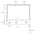
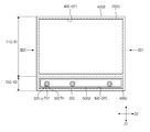
도 2는 도 1에 도시된 액정표시장치의 상면도이고, 도 3은 도 2의 Ⅰ-Ⅰ'를 따라 절단한 단면도이다. 도 2 및 도 3을 참조하여, 상술한 구성들의 배치관계를 좀 더 상세히 설명한다. FIG. 2 is a top view of the liquid crystal display shown in FIG. 1, and FIG. 3 is a cross-sectional view taken along the line II ′ of FIG. 2. 2 and 3, the arrangement of the above-described configuration will be described in more detail.
도 2에 도시된 것과 같이, 상기 표시장치는 평면 상에서 사각형일 수 있다. 도 2에는 상기 2개의 보호부재들(700U, 700L) 중 상기 제1 보호부재(700U)가 도시되어 있다. 제1 액정표시패널(600U)의 테두리는 점선으로 도시되어 있다. As shown in FIG. 2, the display device may be rectangular on a plane. 2 shows the first
상기 제1 보호부재(700U)는 상기 제1 액정표시패널(600U)의 일부분을 커버하는 제1 영역(700-R1)과 상기 제1 영역(700-R1)에 인접한 제2 영역(700-R2)을 포함한다. 상기 제1 개구부(700-OP)는 상기 제1 영역(700-R1)에 구비된다. 상기 제1 개구부(700-OP)를 통해 상기 제1 액정표시패널(600U)의 표시면이 노출된다. 실질적으로 상기 제1 보호부재(700U)의 제1 영역(700-R1)은 상기 제1 액정표시패널(600U)의 테두리 부분을 커버한다. 후술하는 것과 같이, 상기 제1 보호부재(700U)의 제2 영역(700-R2)은 상기 방열부재(300)와 제1 메인회로기판(500U)을 커버한다.The
별도로 도시되지는 않았으나, 상기 표시장치의 배면은 도 2와 실질적으로 동일한 형상을 갖는다. 즉, 제2 보호부재(700L)는 제2 액정표시패널(600L: 도 1 참조)의 일부분을 커버하는 제1 영역(700-R1)과 상기 제1 영역(700-R1)에 인접한 제2 영역(700-R2)을 포함한다. Although not separately illustrated, the rear surface of the display device has a shape substantially the same as that of FIG. 2. That is, the
도 3에 도시된 것과 같이, 상기 도광판(100)은 상기 표시장치의 두께방향(D3)에 있어서, 실질적으로 중앙에 배치된다. 상기 도광판(100)을 중심으로 상측의 구성과 하측의 구성은 실질적으로 동일하다.As shown in FIG. 3, the
상기 도광판(100)은 제1 출사면(110), 상기 제1 출사면(110)에 마주하는 제2 출사면(120), 및 상기 제1 출사면(110)과 상기 제2 출사면(120)을 연결하는 복수 개의 측면들을 구비한다. 예컨대, 평면 상에서 사각형일 때, 상기 도광판(100)은 4개의 측면들을 포함할 수 있다. The
상기 복수 개의 측면들 중 상기 광원(150)으로부터 광을 수신하는 측면은 입사면으로 정의된다. 도 3에는 1개의 입사면(130)이 도시되어 있다. 상기 입사면(130)은 도 2에 도시된 상기 가로방향(D2)으로 연장된다.The side that receives the light from the
상기 제1 출사면(110)으로 출사된 광은 상기 도광판(100)의 상측에 배치된 상기 제1 액정표시패널(600U)에 제공되고, 상기 제2 출사면(120)으로 출사된 광은 상기 도광판(100)의 하측에 배치된 상기 제2 액정표시패널(600L)에 제공된다.The light emitted to the
상기 광원(150)은 유기발광 다이오드와 같은 발광소자(152)와 상기 발광소자(152)에 전기적신호를 제공하는 광원용 회로기판(154)을 포함한다. 상기 광원(150)은 상기 입사면(130)을 따라 상기 가로방향(D2)으로 연장된다. The
상기 발광소자(152)는 복수 개 제공될 수 있고, 상기 복수 개의 발광소자들은 직렬 또는 병렬로 연결된다. 상기 복수 개의 발광소자들(152)은 상기 광원용 회로기판(154)의 일면에 실장된다. A plurality of light emitting
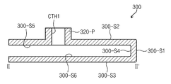
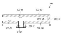
상기 방열부재(300)는 상기 광원(150), 상기 제1 메인회로기판(500U), 및 상기 제2 메인회로기판(500L)을 실장하고, 상기 광원(150), 상기 제1 메인회로기판(500U), 및 상기 제2 메인회로기판(500L)에서 생성된 열을 방출한다.The
도 3에 도시된 것과 같이, 상기 방열부재(300)는 상기 광원(150)에 마주하는 제1 표면(300-S1), 상기 제1 표면(300-S1)으로부터 연장된 제2 표면(300-S2), 상기 제1 표면(300-S1)으로부터 연장된 제3 표면(300-S3)을 포함한다. 상기 제2 표면(300-S2) 및 상기 제3 표면(300-S3) 각각은 상기 제1 표면(300-S1)과 소정의 각도를 이루며 절곡된다. 다만, 상기 제2 표면(300-S2)과 상기 제3 표면(300-S3)은 서로 다른 평면 상에 배치된다. As shown in FIG. 3, the
상기 제1 표면(300-S1)은 상기 입사면(130)에 실질적으로 평행하고, 상기 제2 표면(300-S2)은 상기 제1 출사면(110)에 실질적으로 평행하며, 상기 제3 표면(300-S3)은 상기 제2 출사면(120)에 실질적으로 평행할 수 있다.The first surface 300-S1 is substantially parallel to the
상기 방열부재(300)는 상기 방열부재(300)의 상기 제1 표면(300-S1) 상에 상기 광원(150)을 실장하고, 상기 제2 표면(300-S2) 상에 상기 제1 메인회로기판(500U)을 실장하고, 상기 제3 표면(300-S3) 상에 상기 제2 메인회로기판(500L)을 실장한다. The
상기 광원용 회로기판(154)이 상기 제1 표면(300-S1) 상에 실장된다. 상기 제1 표면(300-S1)과 상기 광원용 회로기판(154)의 타면 사이에 열전달 접착부재(TAS)가 배치된다. 여기서, 상기 광원용 회로기판(154)의 타면은 상기 발광소자(152)가 배치된 일면에 마주하는 면이다. The
상기 열전달 접착부재(TAS)는 접착성분과 접착성분보다 열 전도율이 좋은 열전도 매개체(예컨대 금속, 세라믹, 열 전도성 필러, 또는 금속이 피복된 고분자 성형체)로 구성된다. 상기 접착성분은 상기 광원용 회로기판(154)을 상기 방열부재(300)에 부착시키고, 상기 열전도 매개체는 상기 광원(150)에서 발생한 열을 상기 방열부재(300)에 전달한다.The heat transfer adhesive member (TAS) is composed of an adhesive component and a heat conductive medium having a better thermal conductivity than the adhesive component (for example, metal, ceramic, thermal conductive filler, or metal-coated polymer molded body). The adhesive component attaches the
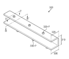
이하, 도 4a 내지 도 4c를 참조하여, 도 3에 도시된 방열부재(300)에 대해 상세히 설명한다. 한편, 상기 방열부재(300)의 형상은 상기 제1 표면(300-S1), 상기 제2 표면(300-S2), 및 상기 제3 표면(300-S3)을 포함하면 충분하며, 다양하게 변형되어 실시될 수 있다. Hereinafter, the
도 4a에 도시된 것과 같이, 상기 방열부재(300)는 수직부(310), 제1 수평부(320), 및 제2 수평부(330)를 포함한다. 상기 수직부(310)는 상기 제1 표면(300-S1)을 구비한다. 상기 제1 수평부(320)는 상기 수직부(310)으로부터 절곡되고 상기 제2 표면(300-S2)을 구비한다. 상기 제2 수평부(330)는 상기 수직부(310)으로부터 절곡되고 상기 제3 표면(300-S3)을 구비한다.As shown in FIG. 4A, the
상기 수직부(310), 상기 제1 수평부(320), 및 상기 제2 수평부(330) 각각은 상기 가로방향(D2)으로 연장된 형상이다. 상기 제1 수평부(320)과 상기 제2 수평부(330)는 서로 이격되어 배치되고, 서로 마주한다. 이때, 상기 방열부재(300)의 단면은 알파벳 "U" 와 유사한 형상을 가질 수 있다. Each of the
한편, 상기 방열부재(300)는 상기 제1 수평부(320)와 상기 제2 수평부(330)를 연결시키고, 상기 수직부(310)와 마주하는 또 다른 수직부를 포함하는 형상으로 변형되어 실시될 수 있다. 이때, 상기 방열부재(300)의 단면은 알파벳 "O" 와 유사한 형상을 가질 수 있다. 상기 방열부재(300)는 상기 제1 표면(300-S1), 상기 제2 표면(300-S2), 및 상기 제3 표면(300-S3)을 포함하는 다른 형상으로 변형될 수 있다.Meanwhile, the
상술한 형상의 방열부재(300)는 상기 제1 표면(300-S1), 상기 제2 표면(300-S2), 및 상기 제3 표면(300-S3)으로 전달받은 열을 다양한 방향으로 방출한다. 상기 방열부재(300)는 상기 제1 표면(300-S1), 상기 제2 표면(300-S2), 및 상기 제3 표면(300-S3)에 각각 마주하는 제4 표면(300-S4), 상기 제5 표면(300-S5), 및 상기 제6 표면(300-S6)으로 열이 방출한다. The
도 4a에 도시된 방열부재(300)는 다양한 방향으로 열을 방출함으로써 방열효율이 증가하며, 상기 수직부(310), 상기 제1 수평부(320), 및 상기 제2 수평부(330)가 서로 다른 평면에 배치됨으로써 작은 공간을 차지한다.The
도 4a 내지 도 4c에 도시된 것과 같이, 상기 제1 수평부(320)는 상기 제2 표면(300-S2)으로부터 돌출된 적어도 하나의 제1 돌출부(320-P)를 포함하고, 상기 제2 수평부(330)는 상기 제3 표면(300-S3)으로부터 돌출된 적어도 하나의 제2 돌출부(330-P)를 포함한다. As shown in FIGS. 4A-4C, the first
이때, 상기 제1 수평부(320)는 상기 제1 돌출부(320-P)의 길이 방향으로 상기 제1 돌출부(320-P)를 관통하는 제1 결합홀(CTH1)를 포함하고, 상기 제2 수평부(330)는 상기 제2 돌출부(330-P)의 길이 방향으로 상기 제2 돌출부(330-P)를 관통하는 제2 결합홀(CTH2)을 포함한다. In this case, the first
한편, 다른 실시예에서, 상기 제1 돌출부(320-P)와 상기 제2 돌출부(330-P)는 상기 제2 표면(300-S2)과 상기 제3 표면(300-S3)을 관통하는 가상선 상에 정렬될 수 있다. 또한, 상기 제1 돌출부(320-P)와 상기 제2 돌출부(330-P) 중 어느 하나 이상은 생략될 수 있다. 또한, 상기 제1 결합홀(CTH1)과 제2 결합홀(CTH2) 역시 생략될 수 있다.Meanwhile, in another embodiment, the first protrusion 320 -P and the second protrusion 330 -P pass through the second surface 300-S2 and the third surface 300-S3. Can be aligned on a line. In addition, any one or more of the first protrusion 320 -P and the second protrusion 330 -P may be omitted. In addition, the first coupling hole CTH1 and the second coupling hole CTH2 may also be omitted.
도 3에 도시된 것과 같이, 상기 제1 돌출부(320-P)는 상기 제1 메인회로기판(500U)을 상기 제1 수평부(320)에 고정시킨다. 도 3에 도시되지는 않았으나, 제1 돌출부(320-P)와 같이, 상기 제2 돌출부(330-P)는 상기 제2 메인회로기판(500L)을 상기 제2 수평부(330)에 고정시킬 수 있다.As shown in FIG. 3, the first protrusion 320 -P fixes the first
상기 제1 메인회로기판(500U)과 상기 제2 메인회로기판(500L)은 적어도 하나의 제1 관통홀(500-TH)을 포함한다. 상기 제1 돌출부(320-P)는 상기 제1 메인회로기판(500U)의 제1 관통홀(500-TH)에 삽입되고, 상기 제2 돌출부(330-P)는 상기 제2 메인회로기판(500L)의 제1 관통홀(미도시)에 삽입된다.The first
또한, 상기 방열부재(300)는 상기 제1 보호부재(700U)에 고정될 수 있다. 상기 제1 보호부재(700U)는 상기 제2 영역(700-R2)에 형성된 제3 결합홀(CTH3)을 포함한다. 상기 제3 결합홀(CTH3)은 상기 제1 결합홀(CTH1)에 대응하는 위치에 형성된다. 상기 방열부재(300)가 상기 제1 보호부재(700U)에 고정되지 않는 다른 실시예에서 상기 제3 결합홀(CTH3)은 생략될 수 있다.In addition, the
고정부재(800)가 상기 제3 결합홀(CTH3)과 상기 제1 결합홀(CTH1)에 삽입된다. 상기 고정부재(800)는 헤드부와 바디부를 포함하는 볼트일 수 있다. 실질적으로 바디부가 상기 제3 결합홀(CTH3)과 상기 제1 결합홀(CTH1)에 삽입된다. 헤드부는 상기 제1 보호부재(700U) 상에 노출된다. 이때, 상기 제1 결합홀(CTH1)의 내벽에는 상기 바디부에 형성된 나사골과 나사산에 대응하는 나사산과 나사골이 형성될 수 있다. The fixing
한편, 볼트의 종류에 따라 상기 제1 결합홀(CTH1)의 내벽의 형상은 변경될 수 있다. 예컨대, 상기 고정부재(800)에 스터드 볼트가 채용되는 경우, 상기 제1 결합홀(CTH1)의 내벽에는 걸림 돌기가 형성된다.The shape of the inner wall of the first coupling hole CTH1 may be changed according to the type of the bolt. For example, when a stud bolt is employed in the fixing
또한, 상기 고정부재(800)는 볼트와 너트로 구성될 수 있다. 너트는 상기 제1 결합홀(CTH1)에 삽입된다. 이때, 상기 제1 결합홀(CTH1)의 내벽에는 나사산과 나사골이 형성되지 않는다. 상기 고정부재(800)가 상기 너트를 포함함으로써 상기 방열부재(300)의 가공은 용이하다.In addition, the fixing
도시되지는 않았으나, 상술한 방식과 동일하게 상기 방열부재(300)는 상기 제2 보호부재(700L)에 고정될 수 있다. 상기 제2 보호부재(700L)는 상기 제2 영역(700-R2)에 형성된 제4 결합홀(CTH4: 도 1 참조)을 더 포함하고, 상기 고정부재(800)가 상기 제4 결합홀(CTH4)과 상기 제2 결합홀(CTH2: 도 4c 참조)에 삽입된다.Although not shown, the
도 5는 도 1에 도시된 액정표시장치에 있어서, 보호 프레임이 제거된 상태의 상면도이고, 도 6a 및 도 6b는 도 5의 측면도이며, 도 7은 도 6b의 일부분을 확대한 도면이다. 이하, 도 5 내지 도 7을 참조하여 상기 지지 프레임에 대해 상세히 설명한다. FIG. 5 is a top view of a state in which a protective frame is removed in the LCD shown in FIG. 1, FIGS. 6A and 6B are side views of FIG. 5, and FIG. 7 is an enlarged view of a portion of FIG. 6B. Hereinafter, the support frame will be described in detail with reference to FIGS. 5 to 7.
도 1 및 도 3을 참조하여 설명한 것과 같이, 상기 지지 프레임은 상기 제1 지지부재(400U)와 상기 제2 지지부재(400L)를 포함한다.As described with reference to FIGS. 1 and 3, the support frame includes the
도 5에는 상기 제1 지지부재(400U), 상기 제1 광학부재(200U), 상기 방열부재(300), 및 상기 제1 메인회로기판(500U)이 도시되었다. 상기 제1 광학부재(200U)의 테두리와 상기 방열부재(300)의 테두리는 점선으로 도시되었다. In FIG. 5, the
상기 제1 지지부재(400U)는 상기 제1 광학부재(200U)의 일부분을 커버하는 제1 영역(400-R1)과 상기 방열부재(300)의 일부분을 커버하는 제2 영역(400-R2)을 포함한다. 상기 제1 광학부재(200U)가 생략되면, 상기 제1 지지부재(400U)의 제1 영역(400-R1)은 상기 도광판(100)의 일부분을 커버한다.The
실질적으로 상기 제1 지지부재(400U)의 제1 영역(400-R1)은 상기 제1 광학부재(200U)의 테두리 부분을 커버하고, 상기 제1 지지부재(400U)의 제2 영역(400-R2)은 상기 방열부재(300)의 테두리 부분을 커버한다.Substantially the first region 400-R1 of the
상기 제1 지지부재(400U)의 제1 영역(400-R1)에 제2 개구부(400-OP1)가 구비되고, 상기 제2 영역(400-R2)에 제3 개구부(400-OP2)가 구비된다.The second opening 400-OP1 is provided in the first region 400-R1 of the first supporting
별도로 도시되지는 않았으나, 상기 제2 지지부재(400L)는 상기 제1 지지부재(400U)와 실질적으로 동일한 형상을 갖는다. 즉, 상기 제2 지지부재(400L)는 상기 제2 광학부재(200L: 도 3 참조)의 일부분을 커버하는 제1 영역(400-R1)과 상기 방열부재(300)의 일부분을 커버하는 상기 제2 영역(400-R2)을 포함한다.Although not separately illustrated, the
도 6a 및 도 6b에 도시된 것과 같이, 상기 제1 지지부재(400U)와 상기 제2 지지부재(400L)는 서로 결합한다. 도 6a는 도 5에 도시된 지지 프레임의 일측면(SD1)은 도 6b는 도 6a에 도시된 일측면과 마주하는 타측면(SD2)을 도시하였다.As shown in FIGS. 6A and 6B, the
도 6a 및 도 6b에 도시된 것과 같이, 상기 제1 지지부재(400U)와 상기 제2 지지부재(400L) 각각은 복수 개의 고리부들(400-R)과 복수 개의 걸림부들(400-P)을 포함한다.As shown in FIGS. 6A and 6B, each of the
상기 복수 개의 고리부들(400-R)은 상기 제1 지지부재(400U)의 상기 일측면(SD1)에 형성된다. 상기 제1 지지부재(400U)의 상기 복수 개의 고리부들(400-R)에 대응하게 상기 복수 개의 걸림부들(400-P)이 상기 제2 지지부재(400L)의 일측면(SD1)에 형성된다. 상기 일측면(SD1)에 구비된 상기 제1 지지부재(400U)의 고리부들(400-R)은 상기 제2 지지부재(400L)의 걸림부들(400-P)에 각각 걸린다.The plurality of ring portions 400 -R are formed on the one side surface SD1 of the
반면에, 상기 제1 지지부재(400U)는 상기 타측면(SD2)에 상기 복수 개의 걸림부들(400-P)이 형성된다. 상기 제1 지지부재(400U)의 상기 걸림부들(400-P)에 대응하게 상기 제2 지지부재(400L)의 타측면(SD2)에 상기 복수 개의 고리부들(400-R)이 형성된다. 상기 타측면(SD2)에 구비된 상기 제2 지지부재(400L)의 고리부들(400-R)은 상기 제1 지지부재(400U)의 걸림부들(400-P)에 각각 걸린다.On the other hand, the first supporting
도 7에 도시된 것과 같이, 상기 걸림부들(400-P) 각각은 적어도 하나의 경사면(400-PS)을 구비한다. 상기 고리부들(400-R) 각각은 대응하는 걸림부(400-P)의 경사면(400-PS)을 따라 압입된다. As shown in FIG. 7, each of the engaging parts 400 -P includes at least one inclined surface 400 -PS. Each of the ring portions 400 -R is press-fitted along the inclined surface 400 -PS of the corresponding catching portion 400 -P.
실질적으로, 상기 제1 지지부재(400U)와 상기 제2 지지부재(400L)의 형상은 동일하다. 상기 제2 지지부재(400L)는 뒤집어진 제1 지지부재(400U)의 형상이다. 실질적으로 상기 지지 프레임은 상기 제1 지지부재(400U)와 뒤집어진 상태의 상기 제1 지지부재(400U)가 결합하여 형성된다. 동일한 형상의 지지부재를 복수개 형성하는 것은 다른 형상의 지지부재들을 형성하는 것보다 지지 프레임의 제조비용이 저렴하다. Substantially, the shape of the
한편, 도 5에 도시된 지지 프레임의 다른 2개의 측면들(도 6a 및 도 6b에 도시되지 않은 측면들) 중 하나는 상기 일측면(SD1)과 동일한 형상을 갖고, 다른 하나는 상기 타측면(SD2)과 동일한 형상을 가질 수 있다.Meanwhile, one of the other two side surfaces (sides not shown in FIGS. 6A and 6B) of the supporting frame illustrated in FIG. 5 has the same shape as the one side surface SD1, and the other side has the other side surface ( It may have the same shape as SD2).
본 발명은 기재된 실시예에 한정되는 것이 아니고, 본 발명의 사상 및 범위를 벗어나지 않고 다양하게 수정 및 변형을 할 수 있음은 이 기술 분야에서 통상의 지식을 가진 자에게는 자명하다. 따라서, 그러한 변형예 또는 수정예들은 본 발명의 특허청구범위에 속한다 해야 할 것이다.It will be apparent to those skilled in the art that various modifications and variations can be made in the present invention without departing from the spirit and scope of the invention as defined in the appended claims. It is therefore intended that such variations and modifications fall within the scope of the appended claims.
100: 도광판 200U, 200L: 광학부재
300: 방열부재 400U, 400L: 지지부재
500U, 500L: 메인회로기판 600U, 600L: 액정표시패널
700U, 700L: 보호부재100:
300:
500U, 500L:
700U, 700L: Protective member
Claims (19)
상기 복수 개의 측면들 중 적어도 어느 하나에 마주하며, 상기 적어도 어느 하나의 측면에 광을 제공하는 광원;
상기 제1 출사면을 통해 출사된 광을 수신하여 이미지를 생성하는 제1 액정표시패널;
상기 제2 출사면을 통해 출사된 광을 수신하여 이미지를 생성하는 제2 액정표시패널;
상기 제1 액정표시패널에 전기적 신호를 제공하는 제1 메인회로기판;
상기 제2 액정표시패널에 전기적 신호를 제공하는 제2 메인회로기판; 및
상기 광원, 상기 제1 메인회로기판, 및 상기 제2 메인회로기판을 실장하며, 상기 광원, 상기 제1 메인회로기판, 및 상기 제2 메인회로기판에서 발생한 열을 방출하는 방열부재를 포함하는 액정표시장치.A light guide plate having a first exit surface, a second exit surface facing the first exit surface, and a plurality of side surfaces connecting the first exit surface and the second exit surface;
A light source facing at least one of the plurality of side surfaces and providing light to the at least one side surface;
A first liquid crystal display panel which receives the light emitted through the first emission surface and generates an image;
A second liquid crystal display panel which receives the light emitted through the second emission surface and generates an image;
A first main circuit board providing an electrical signal to the first liquid crystal display panel;
A second main circuit board providing an electrical signal to the second liquid crystal display panel; And
And a heat dissipation member mounted on the light source, the first main circuit board, and the second main circuit board, and dissipating heat generated from the light source, the first main circuit board, and the second main circuit board. Display.
상기 방열부재는 상기 광원에 마주하는 제1 표면, 상기 제1 표면으로부터 절곡된 제2 표면, 상기 제1 표면으로부터 상기 제2 표면과 다른 방향으로 절곡된 제3 표면을 구비하고,
상기 광원은 상기 제1 표면 상에 실장되고, 상기 제1 메인회로기판은 상기 제2 표면 상에 실장되며, 상기 제2 메인회로기판은 상기 제3 표면 상에 실장된 것을 특징으로 하는 액정표시장치.The method according to claim 1,
The heat dissipation member has a first surface facing the light source, a second surface bent from the first surface, a third surface bent in a direction different from the second surface from the first surface,
The light source is mounted on the first surface, the first main circuit board is mounted on the second surface, and the second main circuit board is mounted on the third surface. .
상기 제1 표면은 상기 복수 개의 측면들 중 상기 적어도 어느 하나의 측면과 실질적으로 평행하고, 상기 제2 표면은 상기 제1 출사면과 실질적으로 평행하며, 상기 제3 표면은 상기 제2 출사면과 실질적으로 평행한 것을 특징으로 하는 액정표시장치.The method of claim 2,
Said first surface is substantially parallel to said at least one of said plurality of sides, said second surface is substantially parallel to said first exit surface, and said third surface is substantially parallel to said second exit surface; A liquid crystal display device, characterized in that substantially parallel.
상기 광원은 복수 개의 발광소자들 및 상기 복수 개의 발광소자들을 실장하는 광원용 회로기판을 포함하고,
상기 광원용 회로기판은 상기 제1 표면 상에 실장되는 것을 특징으로 하는 액정표시장치.The method of claim 2,
The light source includes a plurality of light emitting elements and a circuit board for a light source mounting the plurality of light emitting elements,
And the circuit board for the light source is mounted on the first surface.
상기 방열부재와 상기 광원용 회로기판은 상기 제 1 표면과 상기 광원용 회로기판의 일면 사이에 구비된 열전달 접착부재에 의해서 접착되며, 상시 열전달 접착부재는 상기 광원용 회로기판에서 발생한 열을 상기 방열부재에 전달하는 것을 특징으로 하는 액정표시장치.5. The method of claim 4,
The heat dissipation member and the light source circuit board are bonded by a heat transfer adhesive member provided between the first surface and one surface of the light source circuit board, and the heat transfer adhesive member is configured to radiate heat generated from the light source circuit board. The liquid crystal display device, characterized in that the transfer to the member.
상기 방열부재는 상기 제1 표면을 구비한 수직부, 상기 수직부으로부터 절곡되고 상기 제2 표면을 구비한 제1 수평부, 및 상기 수직부으로부터 절곡되고 상기 제3 표면을 구비한 제2 수평부를 포함하는 것을 특징으로 하는 액정표시장치.The method of claim 2,
The heat dissipation member includes a vertical portion having the first surface, a first horizontal portion bent from the vertical portion and having the second surface, and a second horizontal portion bent from the vertical portion and having the third surface. Liquid crystal display comprising a.
상기 제1 수평부과 상기 제2 수평부는 서로 이격되어 배치되고, 서로 마주하는 것을 특징으로 하는 액정표시장치.The method of claim 6,
And the first horizontal portion and the second horizontal portion are spaced apart from each other and face each other.
상기 제1 액정표시패널의 일부분을 커버하는 제1 영역 및 상기 제1 메인회로기판을 커버하는 제2 영역을 구비하는 제1 보호부재; 및
상기 제2 액정표시패널의 일부분을 커버하는 제1 영역 및 상기 제2 메인회로기판을 커버하는 제2 영역을 구비하고, 상기 제1 보호부재와 결합하는 제2 보호부재를 더 포함하는 것을 특징으로 액정표시장치.The method of claim 6,
A first protection member having a first area covering a portion of the first liquid crystal display panel and a second area covering the first main circuit board; And
And a second protection member having a first area covering a portion of the second liquid crystal display panel and a second area covering the second main circuit board, and coupled to the first protection member. LCD display device.
상기 제1 메인회로기판 및 상기 제2 메인회로기판은 적어도 하나의 제1 관통홀을 각각 포함하고,
상기 방열부재는 상기 제1 메인회로기판의 상기 적어도 하나의 제1 관통홀에 삽입되는 적어도 하나의 제1 돌출부 및 상기 제2 메인회로기판의 상기 적어도 하나의 제1 관통홀에 삽입되는 적어도 하나의 제2 돌출부를 더 포함하는 것을 특징으로 하는 액정표시장치.The method of claim 8,
The first main circuit board and the second main circuit board each include at least one first through hole,
The heat dissipation member may include at least one first protrusion inserted into the at least one first through hole of the first main circuit board, and at least one inserted into the at least one first through hole of the second main circuit board. The liquid crystal display device further comprising a second protrusion.
상기 방열부재는 상기 적어도 하나의 제1 돌출부의 길이 방향으로 상기 적어도 하나의 제1 돌출부를 관통하는 적어도 하나의 제1 결합홀과 상기 적어도 하나의 제2 돌출부의 길이 방향으로 상기 적어도 하나의 제2 돌출부를 관통하는 적어도 하나의 제2 결합홀을 포함하고,
상기 제1 보호부재는 상기 제1 결합홀에 대응하게 상기 제1 보호부재의 상기 제2 영역에 형성된 제3 결합홀을 더 구비하고,
상기 제2 보호부재는 상기 제2 결합홀에 대응하게 상기 제2 보호부재의 상기 제2 영역에 형성된 제4 결합홀을 더 구비하는 것을 특징으로 하는 액정표시장치.10. The method of claim 9,
The heat dissipation member may include at least one first coupling hole penetrating the at least one first protrusion in a length direction of the at least one first protrusion, and the at least one second in a length direction of the at least one second protrusion. At least one second coupling hole penetrating the protrusion,
The first protective member further includes a third coupling hole formed in the second region of the first protective member corresponding to the first coupling hole,
And the second protective member further comprises a fourth coupling hole formed in the second area of the second protective member to correspond to the second coupling hole.
상기 방열부재를 상기 제1 보호부재 및 상기 제2 보호부재 중 어느 하나 이상에 고정시키는 고정부재를 더 포함하고,
상기 고정부재는 상기 제3 결합홀과 상기 제1 결합홀에 삽입되거나, 상기 제4 결합홀과 상기 제2 결합홀에 삽입되는 것을 특징으로 하는 액정표시장치.The method of claim 10,
Fixing member for fixing the heat dissipation member to any one or more of the first protective member and the second protective member,
And the fixing member is inserted into the third coupling hole and the first coupling hole or inserted into the fourth coupling hole and the second coupling hole.
상기 제1 출사면의 일부분과 상기 제2 표면의 일부분을 커버하는 제1 지지부재; 및
상기 제2 출사면의 일부분과 상기 제3 표면의 일부분을 커버하고, 상기 제1 지지부재와 결합하는 제2 지지부재를 더 포함하는 것을 특징으로 액정표시장치.The method of claim 6,
A first support member covering a portion of the first exit surface and a portion of the second surface; And
And a second support member covering a portion of the second exit surface and a portion of the third surface, and coupled to the first support member.
상기 제1 지지부재와 상기 제2 지지부재 각각은 복수 개의 고리부와 복수 개의 걸림부를 포함하며,
상기 제1 지지부재의 상기 복수 개의 고리부들은 상기 제2 지지부재의 상기 복수 개의 걸림부들에 각각 잠기고,
상기 제2 지지부재의 상기 복수 개의 고리부들은 상기 제1 지지부재의 상기 복수 개의 걸림부들에 각각 잠기는 것을 특징으로 하는 액정표시장치.The method of claim 12,
Each of the first and second support members includes a plurality of rings and a plurality of hooks.
The plurality of ring portions of the first support member are respectively locked to the plurality of engaging portions of the second support member,
And the plurality of annular portions of the second support member are locked to the plurality of engaging portions of the first support member, respectively.
상기 제1 지지부재의 형상은 상기 제2 지지부재의 형상과 동일한 것을 특징으로 하는 액정표시장치.The method of claim 13,
The shape of the first support member is the same as the shape of the second support member.
상기 광원으로부터 수신한 광을 제1 출사면과 제2 출사면으로 출사하는 도광판;
상기 제1 출사면에 마주하는 제1 액정표시패널;
상기 제2 출사면에 마주하며, 상기 도광판을 사이에 두고 상기 제1 액정표시패널과 마주하는 제2 액정표시패널;
상기 제1 액정표시패널 및 상기 제2 액정표시패널에 전기적 신호를 제공하는 적어도 하나의 메인회로기판;
상기 광원과 상기 적어도 하나의 메인회로기판을 실장하며, 상기 광원과 상기 적어도 하나의 메인회로기판에서 발생한 열을 방출하는 방열부재;
상기 도광판의 일부분과 상기 방열부재의 일부분을 커버하고, 상기 제1 액정표시패널과 상기 제2 액정표시패널을 지지하는 지지 프레임; 및
상기 제1 액정표시패널, 상기 제2 액정표시패널, 및 상기 지지 프레임를 수용하는 보호 프레임을 포함하는 액정표시장치.A light source for generating light;
A light guide plate configured to emit light received from the light source to a first emission surface and a second emission surface;
A first liquid crystal display panel facing the first exit surface;
A second liquid crystal display panel facing the second emission surface and facing the first liquid crystal display panel with the light guide plate therebetween;
At least one main circuit board providing an electrical signal to the first liquid crystal display panel and the second liquid crystal display panel;
A heat dissipation member mounting the light source and the at least one main circuit board and dissipating heat generated from the light source and the at least one main circuit board;
A support frame covering a portion of the light guide plate and a portion of the heat dissipation member and supporting the first liquid crystal display panel and the second liquid crystal display panel; And
And a protective frame accommodating the first liquid crystal display panel, the second liquid crystal display panel, and the support frame.
상기 방열부재는, 상기 광원을 실장하는 제1 부분 및 상기 적어도 하나의 메인회로기판을 실장하고 상기 제1 부분으로부터 절곡된 적어도 하나의 제2 부분을 구비하는 것을 특징으로 하는 액정표시장치.The method of claim 15,
The heat dissipation member includes a first portion for mounting the light source and at least one second portion for mounting the at least one main circuit board and bent from the first portion.
상기 액정표시장치는 2개의 메인회로기판들을 구비하며,
상기 방열부재는 상기 2개의 메인회로기판들을 각각 실장하는 2개의 제2 부분을 구비하고,
상기 2개의 제2 부분은 서로 이격되고, 서로 마주하는 것을 특징으로 하는 액정표시장치.17. The method of claim 16,
The liquid crystal display device includes two main circuit boards.
The heat dissipation member has two second portions for mounting the two main circuit boards, respectively,
And the two second portions are spaced apart from each other and face each other.
상기 지지 프레임은, 상기 제1 출사면의 일부분을 커버하는 제1 영역과 상기 방열부재의 일부분을 커버하는 제2 영역을 포함하는 제1 지지부재 및 상기 제2 출사면의 일부분을 커버하는 제1 영역과 상기 방열부재의 일부분을 커버하는 제2 영역을 포함하는 제2 지지부재를 포함하고,
상기 제1 지지부재의 상기 제2 영역과 상기 제2 지지부재의 상기 제2 영역 사이에 상기 방열부재가 고정되도록 상기 제1 지지부재는 상기 제2 지지부재에 결합된 것을 특징으로 하는 액정표시장치.The method of claim 15,
The support frame may include a first support member including a first region covering a portion of the first exit surface and a second region covering a portion of the heat radiating member, and a first cover covering a portion of the second exit surface. A second support member comprising a region and a second region covering a portion of said heat dissipation member,
And the first support member is coupled to the second support member such that the heat dissipation member is fixed between the second area of the first support member and the second area of the second support member. .
상기 제1 지지부재의 상기 제1 영역과 상기 제1 출사면 사이에 배치되고, 상기 제1 출사면으로부터 출사된 광의 광학특성을 향상시키는 제1 광학시트; 및
상기 제2 지지부재의 상기 제1 영역과 상기 제2 출사면 사이에 배치되고, 상기 제2 출사면으로부터 출사된 광의 광학특성을 향상시키는 제2 광학시트를 더 포함하는 것을 특징으로 하는 액정표시장치.19. The method of claim 18,
A first optical sheet disposed between the first region of the first support member and the first emission surface, the first optical sheet for improving optical characteristics of light emitted from the first emission surface; And
And a second optical sheet disposed between the first region and the second emission surface of the second support member, the second optical sheet for improving optical characteristics of light emitted from the second emission surface. .
Priority Applications (2)
| Application Number | Priority Date | Filing Date | Title |
|---|---|---|---|
| KR1020120032513A KR20130110491A (en) | 2012-03-29 | 2012-03-29 | Liquid crystal display device |
| US13/602,425 US8958031B2 (en) | 2012-03-29 | 2012-09-04 | Liquid crystal display |
Applications Claiming Priority (1)
| Application Number | Priority Date | Filing Date | Title |
|---|---|---|---|
| KR1020120032513A KR20130110491A (en) | 2012-03-29 | 2012-03-29 | Liquid crystal display device |
Publications (1)
| Publication Number | Publication Date |
|---|---|
| KR20130110491A true KR20130110491A (en) | 2013-10-10 |
Family
ID=49234549
Family Applications (1)
| Application Number | Title | Priority Date | Filing Date |
|---|---|---|---|
| KR1020120032513A KR20130110491A (en) | 2012-03-29 | 2012-03-29 | Liquid crystal display device |
Country Status (2)
| Country | Link |
|---|---|
| US (1) | US8958031B2 (en) |
| KR (1) | KR20130110491A (en) |
Cited By (2)
| Publication number | Priority date | Publication date | Assignee | Title |
|---|---|---|---|---|
| KR20170072678A (en) * | 2015-12-17 | 2017-06-27 | 엘지전자 주식회사 | Display device |
| KR20180016815A (en) * | 2016-08-08 | 2018-02-20 | 엘지전자 주식회사 | Display device |
Families Citing this family (9)
| Publication number | Priority date | Publication date | Assignee | Title |
|---|---|---|---|---|
| KR102029048B1 (en) * | 2011-12-19 | 2019-10-07 | 엘지전자 주식회사 | Display apparatus |
| US20160124268A1 (en) * | 2013-05-15 | 2016-05-05 | Sharp Kabushiki Kaisha | Display device and television receiver |
| TWI494653B (en) * | 2013-06-26 | 2015-08-01 | Au Optronics Corp | Display apparatus |
| CN103605236B (en) | 2013-11-05 | 2017-03-15 | 深圳市华星光电技术有限公司 | Double-side display device and its backlight module |
| US9436037B2 (en) * | 2014-06-20 | 2016-09-06 | Shenzhen China Star Optoelectronics Technology Co., Ltd | Double-sides liquid crystal devices and backlight modules |
| KR102489000B1 (en) * | 2016-02-25 | 2023-01-16 | 엘지전자 주식회사 | Display rotation module and display device comprising it |
| EP3182194B1 (en) * | 2015-12-17 | 2019-06-19 | Lg Electronics Inc. | Display device |
| CN105652519B (en) * | 2016-03-28 | 2018-10-23 | 深圳市华星光电技术有限公司 | A kind of fixed mechanism of display with double faces and its backlight module |
| EP3249452B1 (en) | 2016-05-27 | 2021-03-03 | LG Electronics Inc. | Display device |
Family Cites Families (16)
| Publication number | Priority date | Publication date | Assignee | Title |
|---|---|---|---|---|
| KR100428263B1 (en) | 1996-06-12 | 2004-07-23 | 삼성전자주식회사 | Lcd with dual display panels surrounding a light guide panel |
| WO2003029884A1 (en) | 2001-09-28 | 2003-04-10 | Citizen Watch Co., Ltd. | Liquid crystal display device |
| JP2003255338A (en) | 2002-02-28 | 2003-09-10 | Mitsubishi Electric Corp | Liquid crystal display |
| AU2003233140A1 (en) | 2002-07-08 | 2004-01-23 | Creemers, Tijsbert, M., H. | Foil display with two light guides |
| KR100539836B1 (en) | 2003-03-27 | 2005-12-28 | 엘지.필립스 엘시디 주식회사 | Liquid crystal display device |
| TWI300500B (en) * | 2003-06-03 | 2008-09-01 | Au Optronics Corp | Liquid crystal display |
| CN100390631C (en) | 2003-07-23 | 2008-05-28 | 夏普株式会社 | Liquid crystal display unit |
| TWI351549B (en) | 2004-09-03 | 2011-11-01 | Hon Hai Prec Ind Co Ltd | Backlight module capable of emitting light from tw |
| KR20070098225A (en) | 2006-03-31 | 2007-10-05 | 엘지.필립스 엘시디 주식회사 | Duplex liquid crystal display device |
| US7855764B2 (en) * | 2006-11-02 | 2010-12-21 | Sony Corporation | Electro-optical device and electronic apparatus |
| KR101432567B1 (en) | 2007-04-19 | 2014-08-21 | 엘지디스플레이 주식회사 | Liquid crystal display device |
| US8529111B2 (en) | 2009-02-12 | 2013-09-10 | Nai-Chien Chang | Notebook computer having dual display screens |
| KR101277865B1 (en) * | 2009-12-10 | 2013-06-21 | 엘지디스플레이 주식회사 | Liquid Crystal Display device |
| KR20110077333A (en) | 2009-12-30 | 2011-07-07 | 엘지디스플레이 주식회사 | Dual liquid crystal display device |
| KR20110106499A (en) | 2010-03-23 | 2011-09-29 | 정상원 | Tool for joining driving pcb of flat display |
| KR20110106616A (en) | 2010-03-23 | 2011-09-29 | 삼성전자주식회사 | Dual liquid crystal display apparatus |
-
2012
- 2012-03-29 KR KR1020120032513A patent/KR20130110491A/en not_active Application Discontinuation
- 2012-09-04 US US13/602,425 patent/US8958031B2/en active Active
Cited By (2)
| Publication number | Priority date | Publication date | Assignee | Title |
|---|---|---|---|---|
| KR20170072678A (en) * | 2015-12-17 | 2017-06-27 | 엘지전자 주식회사 | Display device |
| KR20180016815A (en) * | 2016-08-08 | 2018-02-20 | 엘지전자 주식회사 | Display device |
Also Published As
| Publication number | Publication date |
|---|---|
| US20130258246A1 (en) | 2013-10-03 |
| US8958031B2 (en) | 2015-02-17 |
Similar Documents
| Publication | Publication Date | Title |
|---|---|---|
| KR20130110491A (en) | Liquid crystal display device | |
| US9921366B2 (en) | Display with heat radiation | |
| JP5506483B2 (en) | Liquid crystal display device and lighting device | |
| JP5823617B2 (en) | Lighting device, display device, and television receiver | |
| JP4238921B2 (en) | LIGHTING DEVICE, ELECTRO-OPTICAL DEVICE, AND ELECTRONIC DEVICE | |
| KR20140036715A (en) | Display module of display device | |
| JP2012138300A (en) | Television and electronic equipment | |
| JP5779127B2 (en) | Display device and television receiver | |
| JP2014032950A (en) | Light source module and backlight assembly having the same | |
| US9357677B2 (en) | Electronic device with efficient heat radiation structure for electronic components | |
| WO2014181566A1 (en) | Lighting device, display device, and television receiving device | |
| KR101154790B1 (en) | The radiant heat circuit board unified blanket and the chassis structure having the same | |
| KR20120080366A (en) | Light-emitting module, method of manufacturing the same and display apparatus havng the same and | |
| KR101283068B1 (en) | The radiant heat circuit board unified blanket and the backlight unit having the same | |
| US20160154277A1 (en) | Backlight and display apparatus | |
| JP2021167888A (en) | Circuit board and display device with circuit board | |
| WO2013088776A1 (en) | Display device and television receiver | |
| US11949048B2 (en) | Illumination device and display device | |
| KR101372446B1 (en) | TFT module having Multi-layer Back-cover | |
| KR20110127549A (en) | Backlight unit | |
| US10545373B2 (en) | Backlight module and liquid crystal display device | |
| JP2013182164A (en) | Display device and television receiver | |
| KR102057990B1 (en) | The radiant heat circuit board unified blanket and the backlight unit having the same | |
| WO2012111398A1 (en) | Edge-lit lighting device and display device | |
| KR101382847B1 (en) | The chassis structure having the radiant heat circuit board unified blanket and the backlight unit having the same |
Legal Events
| Date | Code | Title | Description |
|---|---|---|---|
| N231 | Notification of change of applicant | ||
| A201 | Request for examination | ||
| E902 | Notification of reason for refusal | ||
| E601 | Decision to refuse application |