WO2021215057A1 - 単結晶製造装置及び単結晶の製造方法 - Google Patents
単結晶製造装置及び単結晶の製造方法 Download PDFInfo
- Publication number
- WO2021215057A1 WO2021215057A1 PCT/JP2021/000220 JP2021000220W WO2021215057A1 WO 2021215057 A1 WO2021215057 A1 WO 2021215057A1 JP 2021000220 W JP2021000220 W JP 2021000220W WO 2021215057 A1 WO2021215057 A1 WO 2021215057A1
- Authority
- WO
- WIPO (PCT)
- Prior art keywords
- single crystal
- diameter
- fusion ring
- camera
- crystal
- Prior art date
- Legal status (The legal status is an assumption and is not a legal conclusion. Google has not performed a legal analysis and makes no representation as to the accuracy of the status listed.)
- Ceased
Links
Images


Classifications
-
- C—CHEMISTRY; METALLURGY
- C30—CRYSTAL GROWTH
- C30B—SINGLE-CRYSTAL GROWTH; UNIDIRECTIONAL SOLIDIFICATION OF EUTECTIC MATERIAL OR UNIDIRECTIONAL DEMIXING OF EUTECTOID MATERIAL; REFINING BY ZONE-MELTING OF MATERIAL; PRODUCTION OF A HOMOGENEOUS POLYCRYSTALLINE MATERIAL WITH DEFINED STRUCTURE; SINGLE CRYSTALS OR HOMOGENEOUS POLYCRYSTALLINE MATERIAL WITH DEFINED STRUCTURE; AFTER-TREATMENT OF SINGLE CRYSTALS OR A HOMOGENEOUS POLYCRYSTALLINE MATERIAL WITH DEFINED STRUCTURE; APPARATUS THEREFOR
- C30B15/00—Single-crystal growth by pulling from a melt, e.g. Czochralski method
- C30B15/20—Controlling or regulating
- C30B15/22—Stabilisation or shape controlling of the molten zone near the pulled crystal; Controlling the section of the crystal
- C30B15/26—Stabilisation or shape controlling of the molten zone near the pulled crystal; Controlling the section of the crystal using television detectors; using photo or X-ray detectors
-
- C—CHEMISTRY; METALLURGY
- C30—CRYSTAL GROWTH
- C30B—SINGLE-CRYSTAL GROWTH; UNIDIRECTIONAL SOLIDIFICATION OF EUTECTIC MATERIAL OR UNIDIRECTIONAL DEMIXING OF EUTECTOID MATERIAL; REFINING BY ZONE-MELTING OF MATERIAL; PRODUCTION OF A HOMOGENEOUS POLYCRYSTALLINE MATERIAL WITH DEFINED STRUCTURE; SINGLE CRYSTALS OR HOMOGENEOUS POLYCRYSTALLINE MATERIAL WITH DEFINED STRUCTURE; AFTER-TREATMENT OF SINGLE CRYSTALS OR A HOMOGENEOUS POLYCRYSTALLINE MATERIAL WITH DEFINED STRUCTURE; APPARATUS THEREFOR
- C30B29/00—Single crystals or homogeneous polycrystalline material with defined structure characterised by the material or by their shape
- C30B29/02—Elements
- C30B29/06—Silicon
-
- G—PHYSICS
- G01—MEASURING; TESTING
- G01B—MEASURING LENGTH, THICKNESS OR SIMILAR LINEAR DIMENSIONS; MEASURING ANGLES; MEASURING AREAS; MEASURING IRREGULARITIES OF SURFACES OR CONTOURS
- G01B11/00—Measuring arrangements characterised by the use of optical techniques
- G01B11/08—Measuring arrangements characterised by the use of optical techniques for measuring diameters
- G01B11/10—Measuring arrangements characterised by the use of optical techniques for measuring diameters of objects while moving
- G01B11/105—Measuring arrangements characterised by the use of optical techniques for measuring diameters of objects while moving using photoelectric detection means
Definitions
- the present invention relates to a single crystal manufacturing apparatus for manufacturing a single crystal by the Czochralski method (hereinafter referred to as CZ method) and a method for manufacturing a single crystal, and more particularly to measuring the diameter of a single crystal during a crystal pulling step. be.
- CZ method Czochralski method
- Most of the silicon wafers used as substrate materials for semiconductor devices are manufactured by the CZ method.
- a polycrystalline silicon raw material is heated in a quartz turret to generate a silicon melt, and a seed crystal is dropped from above the silicon melt and immersed in the silicon melt, and then the seed crystal and the quartz turret are rotated.
- the seed crystal and the quartz turret are rotated.
- By gradually raising the seed crystal while allowing the seed crystal to grow a large single crystal is grown below the seed crystal.
- Single crystal ingots are manufactured aiming at a certain diameter. For example, if the final product is a 300 mm wafer, it is common to grow a single crystal ingot of 305 to 320 mm, which is slightly larger than the diameter. After that, the single crystal ingot is externally ground into a columnar shape, sliced into a wafer shape, and then subjected to a chamfering process to finally obtain a wafer having a target diameter. As described above, the target diameter of the single crystal ingot must be larger than the wafer diameter of the final product, but if it is too large, the grinding allowance increases and it becomes uneconomical. Therefore, a single crystal ingot that is larger than the wafer and has a diameter as small as possible is required.
- Patent Document 1 describes a method of accurately measuring the diameter of a growing single crystal by processing an image of the interface between the single crystal and the melt. In this method, the rutsubo rotation speed, the crystal rotation speed, the crystal pulling speed, the rutsubo rising speed, the melt temperature (heater power), and the like are controlled so that the diameter of the single crystal becomes the target diameter.
- Patent Document 2 relates to the measurement of the melt level position, and is a real image of the furnace structure in the chamber and the image of the melt level taken when the liquid level of the melt is photographed by a camera installed outside the chamber. And a method of calculating the representative dimensions of the mirror image are described.
- the edge patterns of the real image of the furnace structure reflected in the photographed image and the mirror image of the furnace structure reflected on the liquid surface of the melt are detected, and the inside of the furnace is based on the camera installation angle and focal distance.
- a reference that maximizes the matching rate when the edge patterns of the real image and mirror image of the structure are projected and converted onto the reference plane and the edge patterns of the real image and mirror image of the furnace structure on the reference plane are matched. From the shape of the pattern, the representative dimensions of the real image and the mirror image of the structure inside the furnace are calculated.
- the diameter of the single crystal is measured from the image taken by the camera installed outside the furnace, and the diameter of the single crystal is controlled so that the measured value of the diameter matches the diameter profile. Accurate diameter measurement is required.
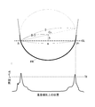
- a scanning line SL for measuring the diameter in the horizontal direction is set in the camera image, and from the intersection of the brightness distribution on the scanning line SL and the threshold value TH (slice level). The edge of the fusion ring FR is detected.
- the diameter of the fusion ring is used by using the width w between the two intersections p L and p R of the scanning line SL and the edge of the fusion ring FR and the distance h from the crystal center position C 0 to the scanning line SL.
- D 2 (w 2 + 4h 2 ) 1/2 . Since the unit of the diameter value D of the fusion ring thus obtained is the number of pixels (pixels), the crystal diameter value converted into the actual unit (mm) can be obtained by multiplying the diameter D by the diameter conversion coefficient.
- the crystal diameter information obtained from the camera image is a pixel, it is necessary to convert it into an actual diameter unit (mm).
- the diameter conversion coefficient used for unit conversion is created based on the crystal diameter value visually measured by the operator with a telescope during the single crystal pulling process, the unit conversion accuracy is poor and the diameter calculation error. There is a problem that is large.
- an object of the present invention is to provide a single crystal manufacturing apparatus and a manufacturing method capable of improving the measurement accuracy of the crystal diameter.
- the single crystal manufacturing apparatus includes a single crystal pulling portion for pulling a single crystal from a melt and a camera for photographing a fusion ring generated at a boundary portion between the melt and the single crystal.
- the calculation unit includes a calculation unit that processes a captured image of the camera, and the calculation unit attaches the fusion ring to the captured image of the camera to the liquid surface of the melt based on the installation angle and focal length of the camera. It is characterized in that the diameter of the single crystal is calculated from the shape of the fusion ring on the reference plane by projection conversion on the corresponding reference plane.
- the actual diameter of a single crystal can be accurately obtained without using the diameter conversion coefficient for unit-converting the diameter measurement value obtained from the image taken by the camera. Therefore, it is possible to improve the measurement accuracy of the diameter of the single crystal during the crystal pulling step.
- the calculation unit projects and transforms the edge pattern of the fusion ring detected based on a predetermined threshold value for the brightness distribution of the captured image onto the reference plane. As a result, the shape of the fusion ring can be accurately grasped.
- the threshold value is a value obtained by multiplying the peak value of brightness in the captured image by a value smaller than 1, and the calculation unit performs horizontal scanning intersecting with the fusion ring in the captured image. It is preferable to set a line and detect the outer intersection of the luminance distribution on the horizontal scanning line and the threshold value (one point near the outer periphery of the captured image) as the edge pattern of the fusion ring.
- the calculation unit determines the distance between two intersections of the edge pattern of the fusion ring projected on the reference plane and a predetermined diameter measurement line, and from the center position of the single crystal to the diameter measurement line. It is preferable to calculate the diameter of the single crystal from the distance of. Thereby, the diameter of the fusion ring can be calculated geometrically, and the diameter of the single crystal can be calculated from the diameter of the fusion ring.
- the calculation unit approximates the edge pattern of the fusion ring to a circle and calculates the diameter of the single crystal from the diameter of the approximate circle of the fusion ring. As a result, the accuracy of measuring the diameter of the fusion ring can be improved.
- the calculation unit subtracts a predetermined correction amount from the diameter during the pulling step of the single crystal, or multiplies the diameter during the pulling step of the single crystal by a predetermined correction coefficient. It is preferable to calculate the diameter of the crystal at room temperature. Thereby, the crystal diameter can be controlled based on the diameter of the single crystal at room temperature.
- the calculation unit changes the correction amount or the correction coefficient according to a change in the furnace structure, the position of the liquid level, or the length of the single crystal.
- the crystal diameter can be accurately measured according to the change in the growing condition of the single crystal.
- the method for producing a single crystal according to the present invention is a method for producing a single crystal by the CZ method, in which a step of photographing a fusion ring generated at a boundary between a melt and a single crystal with a camera and an image of the camera.
- the step of calculating the diameter of the single crystal includes the step of processing the image and calculating the diameter of the single crystal, and the step of calculating the diameter of the single crystal is the fusion captured in the image taken by the camera based on the installation angle and the focal distance of the camera.
- the ring is projected and transformed onto a reference plane corresponding to the liquid surface of the melt, and the diameter of the single crystal is calculated from the shape of the fusion ring on the reference plane.
- the actual diameter of a single crystal can be accurately obtained without using the diameter conversion coefficient for unit-converting the diameter measurement value obtained from the image taken by the camera. Therefore, it is possible to improve the measurement accuracy of the diameter of the single crystal during the crystal pulling step.
- the step of calculating the diameter of the single crystal in the step of calculating the diameter of the single crystal, it is preferable to project and convert the edge pattern of the fusion ring detected based on a predetermined threshold value with respect to the brightness distribution of the photographed image onto the reference plane. .. As a result, the shape of the fusion ring can be accurately grasped.
- the threshold value is a value obtained by multiplying the peak value of brightness in the captured image by a value smaller than 1, and the step of calculating the diameter of the single crystal is the fusion in the captured image. It is preferable to set a horizontal scanning line that intersects the ring and detect the outer intersection of the luminance distribution on the horizontal scanning line and the threshold value (one point near the outer periphery of the captured image) as the edge pattern of the fusion ring.
- the step of calculating the diameter of the single crystal is the distance between the two intersections of the edge pattern of the fusion ring projected on the reference plane and the predetermined diameter measurement line and the center position of the single crystal. It is preferable to calculate the diameter of the single crystal from the distance from the diameter to the diameter measurement line. Thereby, the diameter of the fusion ring can be calculated geometrically, and the diameter of the single crystal can be calculated from the diameter of the fusion ring.
- the edge pattern of the fusion ring is approximated by a circle and the diameter of the single crystal is calculated from the diameter of the approximate circle of the fusion ring. As a result, the accuracy of measuring the diameter of the fusion ring can be improved.
- the step of calculating the diameter of the single crystal is to subtract a predetermined correction amount from the diameter during the pulling step of the single crystal, or to multiply the diameter during the pulling step of the single crystal by a predetermined correction coefficient. Therefore, it is preferable to calculate the diameter of the single crystal at room temperature. Thereby, the crystal diameter can be controlled based on the diameter of the single crystal at room temperature.
- the crystal diameter of the single crystal in the step of calculating the diameter of the single crystal, it is preferable to change the correction amount or the correction coefficient according to a change in the structure inside the furnace, the position of the liquid level, or the length of the single crystal. .. As a result, the crystal diameter can be accurately measured according to the change in the growing condition of the single crystal.
- the present invention it is possible to provide a single crystal manufacturing apparatus and a manufacturing method capable of improving the measurement accuracy of the crystal diameter.
- FIG. 1 is a schematic cross-sectional view showing the configuration of a single crystal manufacturing apparatus according to an embodiment of the present invention.
- FIG. 2 is a flowchart for explaining a method for manufacturing a silicon single crystal using a single crystal manufacturing apparatus.
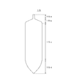
- FIG. 3 is a side view showing the shape of the silicon single crystal ingot manufactured by the manufacturing method of FIG.
- FIG. 4 is a photographed image of the camera 18 and is a diagram for explaining a fusion ring generated at the solid-liquid interface.
- FIG. 5 is a schematic diagram for explaining a method of projecting and converting the two-dimensional coordinates of the captured image into the coordinates of the real space.
- FIG. 6 is a diagram for explaining a diameter calculation method according to the present embodiment.
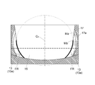
- Figure 7 is a schematic diagram for explaining a method for calculating a gap value ⁇ G radius r f of the real image Ma and mirror Mb respective openings of the heat insulating member 17, the r m.
- FIG. 8 is a diagram for explaining a conventional diameter calculation method.
- FIG. 1 is a schematic cross-sectional view showing the configuration of a single crystal manufacturing apparatus according to an embodiment of the present invention.
- the single crystal manufacturing apparatus 10 is an apparatus for growing a silicon single crystal, includes a substantially cylindrical chamber 19, and quartz in which the silicon melt 13 is stored inside the chamber 19.
- the crucible 11 is installed.
- the chamber 19 may have, for example, a double-walled structure having a certain gap formed inside, and by flowing cooling water through the gap, it is possible to prevent the chamber 19 from becoming hot when the quartz crucible 11 is heated. ..
- An inert gas such as argon is introduced into the chamber 19 from before the start of pulling up the silicon single crystal to after the end.
- a pull-up drive 22 is provided at the top of the chamber 19.
- the pulling drive device 22 pulls up the seed crystal 14 that is the growth nucleus of the silicon single crystal ingot 15 and the silicon single crystal ingot 15 that grows from the seed crystal 14 while rotating it.
- the pulling drive device 22 may be formed with a sensor (not shown) that transmits crystal length information of the silicon single crystal ingot 15 based on the amount of pulling of the silicon single crystal ingot 15.
- the pulling drive device 22 is connected to the control unit 26, and the crystal length information is sent to the control unit 26.
- the components in the chamber 19 such as the quartz crucible 11 and the pulling drive device 22 constitute a single crystal pulling portion.
- a substantially cylindrical heater 12 arranged so as to surround the quartz crucible 11 is provided inside the chamber 19.
- the heater 12 heats the quartz crucible 11.
- a crucible support (graphite crucible) 16 and a quartz crucible 11 are housed inside the heater 12.
- the quartz crucible 11 is a substantially cylindrical container in which the whole is integrally formed of quartz and the upper part forms an open surface.
- a silicon melt 13 in which solid silicon is melted is stored in the quartz crucible 11.
- the crucible support 16 is entirely made of graphite and is closely supported so as to wrap the quartz crucible 11.
- the crucible support 16 maintains the shape of the quartz crucible 11 softened when the silicon is melted, and plays a role of supporting the quartz crucible 11.
- a crucible lift device 21 is provided under the crucible support 16.
- the crucible lift device 21 supports the crucible support 16 and the quartz crucible 11 from below, and the liquid level position of the melt surface 13a of the silicon melt 13 that changes as the silicon single crystal ingot 15 is pulled up is an appropriate position.
- the quartz crucible 11 is moved up and down so as to be. Thereby, the position of the melt surface 13a of the silicon melt 13 is controlled.
- the crucible lift device 21 rotatably supports the crucible support 16 and the quartz crucible 11 at a predetermined rotation speed when the crucible is pulled up.
- a heat shield member (shielding cylinder) 17 is formed on the upper surface of the quartz crucible 11 so as to cover the upper surface of the silicon melt 13, that is, the melt surface 13a.
- the heat shield member 17 is made of, for example, a mortar-shaped heat insulating plate, and a substantially circular opening 17a is formed at the lower end thereof. The outer edge of the upper end of the heat shield member 17 is fixed to the inner surface side of the chamber 19.
- Such a heat shield member 17 prevents the pulled-up silicon single crystal ingot 15 from receiving radiant heat from the silicon melt 13 in the quartz crucible 11 to change the heat history and deteriorate the quality. Further, such a heat shield member 17 induces the pulling atmosphere gas introduced into the chamber 19 from the silicon single crystal ingot 15 side to the silicon melt 13 side, thereby causing the vicinity of the melt surface 13a of the silicon melt 13. The amount of residual oxygen, silicon vapor evaporated from the silicon melt 13, SiO, and the like are controlled so that the silicon single crystal ingot 15 has the desired quality. It is considered that the control of such a raised atmosphere gas depends on the pressure inside the furnace and the flow velocity when passing through the gap between the lower end of the heat shield member 17 and the melt surface 13a of the silicon melt 13.
- an inert gas such as argon may contain hydrogen, nitrogen, or any other predetermined gas as the dopant gas.
- a camera 18 is installed on the outside of the chamber 19.
- the camera 18 is, for example, a CCD camera, and photographs the inside of the chamber 19 through a viewing window formed in the chamber 19.
- the installation angle ⁇ c of the camera 18 is a predetermined angle with respect to the pulling axis Z of the silicon single crystal ingot 15, and the camera 18 has an optical axis L inclined with respect to the vertical direction.
- the installation angle ⁇ c of the camera 18 is the inclination angle of the optical axis L with respect to the vertical direction.
- the camera 18 photographs the upper surface region of the quartz crucible 11 including the opening 17a of the heat shield member 17 and the melt surface 13a from diagonally above.
- the camera 18 is connected to the calculation unit 24, and the captured image of the camera 18 is used by the calculation unit 24 to detect the crystal diameter and the liquid level position.
- the calculation unit 24 uses the silicon melt 13 based on an image including a real image of the heat shield member 17 taken by the camera 18 and a mirror image of the heat shield member 17 projected on the melt surface 13a of the silicon melt 13. Calculate the liquid level position of. Further, the calculation unit 24 calculates the diameter of the silicon single crystal ingot based on the image including the boundary portion between the silicon melt 13 and the silicon single crystal ingot 15 taken by the camera 18. The calculation unit 24 is connected to the control unit 26, and the calculation result is sent to the control unit 26 by the calculation unit 24.
- the control unit 26 moves the quartz rut pot 11 (rise amount) based on the crystal length data of the silicon single crystal ingot 15 obtained from the sensor of the pulling drive device 22 and the crystal diameter data calculated by the calculation unit 24. ) Is controlled. Further, in order to control the movement amount of the quartz crucible 11, the control unit 26 performs position correction control of the quartz crucible 11 based on the liquid level position of the silicon melt 13 calculated by the calculation unit 24.
- FIG. 2 is a flowchart for explaining a method for manufacturing a silicon single crystal using the single crystal manufacturing apparatus 10. Further, FIG. 3 is a side view showing the shape of the silicon single crystal ingot manufactured by the manufacturing method of FIG.
- the raw material polycrystalline silicon is put into the quartz rutsubo 11, the polycrystalline silicon in the quartz rutsubo 11 is heated and melted by the heater 12, and the silicon melt 13 is produced. Is generated (step S11).
- step S12 the seed crystal 14 is lowered and landed on the silicon melt 13 (step S12). Then, a crystal pulling step (steps S13 to S16) is carried out in which the seed crystal 14 is gradually pulled up while maintaining the contact state with the silicon melt 13 to grow a single crystal.
- the straight body part growing step S15 for forming the straight body part 15c in which the crystal diameter is maintained at a specified diameter (for example, about 300 mm) and the tail part growing step S16 for forming the tail part 15d in which the crystal diameter is gradually reduced are performed. It is carried out in order, and finally the single crystal is separated from the melt surface. As a result, the silicon single crystal ingot 15 shown in FIG. 3 having a neck portion 15a, a shoulder portion 15b, a straight body portion 15c, and a tail portion 15d is completed.
- the gap value ⁇ G between the melt surface 13a of the silicon melt 13 and the heat shield member 17 is calculated from the image taken by the camera 18, and the liquid level position of the silicon melt 13 is calculated from this. Then, the amount of increase in the crucible is controlled based on this gap value ⁇ G. As a result, the position of the melt surface 13a with respect to the structure inside the furnace such as the heater 12 and the heat shield member 17 is kept constant from the start to the end of the pulling of the silicon single crystal regardless of the decrease of the silicon melt 13. By changing this, the radiation distribution of heat with respect to the silicon melt 13 can be controlled.
- the diameter of the single crystal is calculated from the image taken by the camera 18, and the crystal pulling condition is controlled so that the crystal diameter becomes a predetermined diameter corresponding to the crystal length.
- the crystal diameter is controlled to be gradually increased
- the crystal diameter is controlled to be constant
- the crystal diameter is gradually reduced.
- the control target of the crystal pulling condition is the height position of the quartz crucible 11, the crystal pulling speed, the heater output, and the like.
- the control of the pulling condition using the captured image of the camera 18 is performed during the crystal pulling step. Specifically, it is performed between the start of the necking step S13 in FIG. 2 and the end of the tail portion growing step S16.
- FIG. 4 is a photographed image of the camera 18 and is a diagram for explaining a fusion ring generated at the solid-liquid interface.
- the silicon melt 13 can be seen through the opening 17a of the heat shield member 17, and a part of the heat shield member 17 is reflected in the photographed image. Further, there is a silicon single crystal 15 inside the opening 17a of the heat shield member 17, and the silicon melt 13 can be peeked through a slight gap between the heat shield member 17 and the silicon single crystal 15. Further, a fusion ring FR is generated at the boundary between the silicon single crystal 15 and the silicon melt 13.
- the fusion ring FR is a ring-shaped high-luminance region generated by reflecting the radiated light from the heater 12 and the like by the meniscus at the solid-liquid interface.
- the heat shield member 17 since the heat shield member 17 is fixed to the chamber 19, its position does not change, but the position and size of the fusion ring FR change depending on the change in the crystal diameter and the liquid level position.
- the larger the crystal diameter the larger the fusion ring FR.
- the crystal diameter decreases as the liquid level position decreases. In this way, since the outline of the single crystal in the vicinity of the solid-liquid interface can be captured from the fusion ring FR, the diameter of the single crystal can be calculated.
- a mirror image Mb of the heat shield member 17 is reflected on the melt surface 13a of the silicon melt 13.
- the mirror image Mb of the heat shield member 17 changes according to the distance from the heat shield member 17 to the melt surface 13a. Therefore, the distance between the real image Ma of the heat shield member 17 and the mirror image Mb reflected on the melt surface 13a is due to the consumption of the silicon melt 13 due to crystal growth and the vertical movement of the melt surface 13a due to the elevating and lowering of the quartz ruts 11. Although interlocked, the position of the melt surface 13a is at the midpoint between the real image Ma and the mirror image Mb.
- the distance between the real image Ma and the mirror image Mb of the heat shield member 17 becomes zero, and when the melt surface 13a is gradually lowered, the heat shield is generated.
- the distance (gap value) ⁇ G from the lower end of the member 17 to the melt surface 13a also gradually increases.
- the liquid level position of the silicon melt 13 can be obtained as a distance from the lower end of the heat shield member 17.
- the edge pattern of the fusion ring FR is detected from the image taken by the camera 18, and the crystal diameter is calculated from the edge pattern of the fusion ring FR.
- the diameter value of the fusion ring FR can be obtained from an approximate circle obtained by approximating the edge pattern (sample value) by the least squares method. By further correcting the diameter of the fusion ring FR thus obtained, the diameter of the single crystal at room temperature can be calculated.
- the threshold value (slice level) is changed according to the brightness of the fusion ring FR in the image to reduce the measurement error due to the influence of the brightness change.
- a horizontal scanning line SL that intersects the fusion ring FR is set as in FIG. 8, and an outer intersection (photographing) between the brightness distribution on the horizontal scanning line SL and the threshold value (corresponding to TH in FIG. 8) is set.
- One point near the outer periphery of the image) is detected as the edge of the fusion ring FR.
- the edge pattern of the fusion ring FR photographed by the camera 18 is projected and transformed on the reference plane, and the diameter of the fusion ring FR when viewed from directly above is obtained.
- the reference plane is the liquid level (horizontal plane) of the silicon melt 13, and can be obtained from the real image Ma and the mirror image Mb of the heat shield member 17 as described above.
- FIG. 5 is a schematic diagram for explaining a method of projecting and converting the two-dimensional coordinates of a photographed image into the coordinates of the real space.
- the shape of the fusion ring in the captured image is distorted, resulting in an image with a sense of perspective. .. That is, the image on the lower side, which is close to the camera 18, is wider than the image on the upper side. Therefore, in order to accurately calculate the dimensions of the fusion ring, it is necessary to correct the distortion of the image. Therefore, the coordinates of the captured image of the camera 18 are projected and transformed into the coordinates on the reference plane set at the same height position as the melt surface 13a to correct the distortion.
- the figure on the right side of FIG. 5 shows a coordinate system for performing image correction.
- the reference plane is the xy plane.
- the origin C 0 of the XY coordinates passes from the center position C (0, y c , z c ) of the image pickup device 18 a of the camera 18 to the center position F (0, y f , z f ) of the lens 18 b of the camera 18. It is the intersection of the straight line (single point chain line) drawn in and the reference plane. This straight line is the optical axis of the camera 18.
- the pulling direction of the silicon single crystal 15 is the positive direction of the z-axis, which is the vertical axis, and the center position C (0, y c , z c ) of the imaging device 18a and the center position F (0, y) of the lens 18b. f , z f ) is in the yz plane.
- the coordinates (u, v) in the image shown on the left side of FIG. 5 are represented by the pixels of the image pickup device 18a, and any one point P (x p , y) on the image pickup device 18a shown in the following equation (1). It corresponds to p , z p).
- ⁇ u and ⁇ v are the pixel sizes in the horizontal and vertical directions of the imaging device 18a
- y c and z c are the y and z coordinates of the center position C of the imaging device 18a.
- ⁇ c is an angle formed by the optical axis of the camera 18 with the z axis, and is an installation angle of the camera 18.
- the official imaging lens the focal length f l is the distance a, with b is expressed by the following equation (5).
- any one point P (x p , x p , x p ) on the imaging device 18a is projected onto the reference plane through F (0, y f , z f), and this projection
- the point P'(X, Y, 0) can be represented by the following equation (8).
- the projection point P'(X) is used by using the value of the back distance. , Y, 0) can be represented.
- the least squares method may be used as a method for calculating the coordinates (x 0 , y 0 ) and radius r of the center position from the coordinates of the fusion ring projected on the reference plane.
- the fusion ring is circular, and its image satisfies the equation of the circle shown in the following equation (10).
- the least squares method is used to calculate (x 0 , y 0 ) and r in the equation (10).
- the transformation shown in the following equation (11) is performed.
- the variables a, b, and c in this equation (11) are obtained by the least squares method. It is obtained by obtaining the condition that the sum of squares of the difference between the equation (11) and the measured point is minimized, and solving this by solving the partial differential equation shown in the following equation (12).
- the diameter is calculated from the approximate circle of the fusion ring.
- the silicon single crystal in the crystal pulling process is thermally expanded at a high temperature, its diameter is larger than the diameter when it is taken out from the chamber 19 and cooled.
- the diameter of a silicon single crystal is controlled based on such a thermally expanded crystal diameter, it is difficult to control the crystal diameter at room temperature to be the target diameter.
- the diameter of the silicon single crystal shown in the image taken by the camera 18 at high temperature is converted into the diameter at room temperature, and based on the crystal diameter at room temperature.
- the crystal growth conditions such as the crystal pulling rate are controlled.
- the reason for controlling the crystal pulling condition based on the crystal diameter at room temperature is that it is important to control the crystal diameter at room temperature. That is, even if the diameter is raised according to the target diameter at high temperature, if the diameter is smaller than the target diameter when the temperature is returned to room temperature, it may not be possible to commercialize the product. Therefore, the crystal diameter at room temperature is the target diameter.
- the diameter is controlled as follows.
- the diameter of the silicon single crystal at room temperature can be obtained by subtracting a predetermined correction amount from the diameter of the single crystal obtained from the fusion ring at high temperature.
- the diameter of the silicon single crystal at room temperature may be obtained by multiplying the diameter of the single crystal obtained from the fusion ring at high temperature by a predetermined correction coefficient. Since the correction amount or correction coefficient at this time differs depending on the structure inside the furnace, it is set individually for each single crystal pulling device. When the structure inside the furnace changes with the crystal growth, the correction amount or the correction coefficient may be changed according to the crystal growth. Further, the correction amount or correction coefficient of the crystal diameter may be changed according to the change in the liquid level position of the silicon melt, or may be set according to the pulling length of the single crystal.
- a certain correction amount may be used to correct the crystal diameter
- another correction amount may be used to correct the crystal diameter.
- the correction amount is the crystal diameter during the pulling process by the camera obtained for the same crystal. It is calculated in advance based on the measurement result and the measurement result of the crystal diameter measured at room temperature. Further, when the crystal diameter at room temperature is obtained by multiplying the crystal diameter measurement result by the camera by a predetermined correction coefficient, the correction coefficient is the crystal obtained for the same crystal during the pulling process by the camera. It is calculated in advance based on the measurement result of the diameter and the measurement result of the crystal diameter measured at room temperature. In any of the above methods, the correction amount or the correction coefficient at the diameter measurement positions that match in the crystal longitudinal direction is calculated in consideration of the amount of the single crystal extending in the longitudinal direction due to thermal expansion during the crystal pulling process. ..
- Figure 7 is a schematic diagram for explaining a method for calculating a gap value ⁇ G radius r f of the real image Ma and mirror Mb respective openings of the heat insulating member 17, the r m.
- the center coordinates of the mirror image of the heat shield member 17 are originally the center coordinates of the real image of the heat shield member 17 with the melt surface 13a in between (X). It exists on the opposite side of hc , Y hc , 0), and the straight line connecting the two points passes through the center coordinates (X hc , Y hc , 0) of the real image of the heat shield member 17 and is parallel to the Z axis, which is the vertical axis. It becomes a straight line.
- the center coordinates (X mc , Y mc , 0) of the mirror image of the heat shield member 17 on the reference plane are such that the center coordinates (X mc , Y mc , Z gap ) of the mirror image of the heat shield member 17 are on the reference plane. Since the coordinates are projected on, the center coordinates of the mirror image (X hc , Y hc , Z gap ) are the center coordinates (X mc , Y mc , 0) of the mirror image of the heat shield member 17 on the reference plane and the lens. It is on a straight line passing through the center position F (X f , Y f , Z f) of 18b. Therefore, the gap ⁇ G to be calculated is half the value of Zgap, and can be calculated from the following equation (14).
- the gap value ⁇ G can be expressed as in Eq. (16).
- Mirror image of the heat insulating member 17 reflected in the melt surface 13a can be considered to be distant by 2 ⁇ G than the actual heat insulating member 17, the radius r m is a real image of the radius r f of the mirror image of that for the heat insulating member 17 Looks smaller than. Further, it is known that the size of the opening of the heat shield member 17 is larger than the size at room temperature due to thermal expansion under the temperature environment in the furnace during crystal pulling.
- the opening in consideration of the thermal expansion radius (theoretical value) r actual are, real image of the radius measurements r f of the opening of the heat insulating member 17, and the radius measurements of the opening of the mirror image of the heat insulating member 17 r m Then, the distances L f and L m can be calculated by the following equation (17).
- the gap value ⁇ G can be calculated as the following equation (18).
- the gap value ⁇ G is the radius measured values r f of a real image and a mirror image respective openings of the heat insulating member 17, can be obtained from r m.
- the method for producing a silicon single crystal processes a photographing step of photographing a fusion ring generated at a boundary between a silicon melt and a silicon single crystal with a camera, and processing an image captured by the camera.
- Te and a crystal diameter calculating step of calculating the diameter of a silicon single crystal crystal diameter calculating step, based on the installation angle theta c and focal length f l camera, a fusion ring caught on an image captured by a camera of the melt Since the diameter of the single crystal is calculated from the shape of the fusion ring on the reference plane by projection conversion on the reference plane corresponding to the liquid level position, the diameter measurement value obtained from the image taken by the camera is converted into units. The actual diameter of a single crystal can be accurately obtained without using the diameter conversion coefficient of. Therefore, the crystal diameter can be accurately measured and controlled in the crystal pulling step, whereby the production yield of the silicon single crystal can be increased.
- the production of a silicon single crystal has been mentioned as an example, but the present invention is not limited to this, and can be applied to the production of various single crystals grown by the CZ method.
Landscapes
- Chemical & Material Sciences (AREA)
- Engineering & Computer Science (AREA)
- Crystallography & Structural Chemistry (AREA)
- Materials Engineering (AREA)
- Metallurgy (AREA)
- Organic Chemistry (AREA)
- Physics & Mathematics (AREA)
- General Physics & Mathematics (AREA)
- Crystals, And After-Treatments Of Crystals (AREA)
Priority Applications (5)
| Application Number | Priority Date | Filing Date | Title |
|---|---|---|---|
| DE112021002436.1T DE112021002436T5 (de) | 2020-04-20 | 2021-01-06 | Vorrichtung und Verfahren zur Herstellung von Einkristallen |
| US17/996,737 US20230220583A1 (en) | 2020-04-20 | 2021-01-06 | Single crystal production apparatus and single crystal production method |
| KR1020227035290A KR102696535B1 (ko) | 2020-04-20 | 2021-01-06 | 단결정 제조 장치 및 단결정의 제조 방법 |
| JP2022516846A JP7435752B2 (ja) | 2020-04-20 | 2021-01-06 | 単結晶製造装置及び単結晶の製造方法 |
| CN202180029654.5A CN115461500B (zh) | 2020-04-20 | 2021-01-06 | 单晶制造装置及单晶的制造方法 |
Applications Claiming Priority (2)
| Application Number | Priority Date | Filing Date | Title |
|---|---|---|---|
| JP2020-074514 | 2020-04-20 | ||
| JP2020074514 | 2020-04-20 |
Publications (1)
| Publication Number | Publication Date |
|---|---|
| WO2021215057A1 true WO2021215057A1 (ja) | 2021-10-28 |
Family
ID=78270418
Family Applications (1)
| Application Number | Title | Priority Date | Filing Date |
|---|---|---|---|
| PCT/JP2021/000220 Ceased WO2021215057A1 (ja) | 2020-04-20 | 2021-01-06 | 単結晶製造装置及び単結晶の製造方法 |
Country Status (7)
| Country | Link |
|---|---|
| US (1) | US20230220583A1 (https=) |
| JP (1) | JP7435752B2 (https=) |
| KR (1) | KR102696535B1 (https=) |
| CN (1) | CN115461500B (https=) |
| DE (1) | DE112021002436T5 (https=) |
| TW (1) | TWI770661B (https=) |
| WO (1) | WO2021215057A1 (https=) |
Cited By (3)
| Publication number | Priority date | Publication date | Assignee | Title |
|---|---|---|---|---|
| CN114252018A (zh) * | 2021-12-29 | 2022-03-29 | 西安奕斯伟材料科技有限公司 | 晶体直径检测方法、系统及计算机程序产品 |
| WO2023195217A1 (ja) * | 2022-04-08 | 2023-10-12 | 株式会社Sumco | シリコン単結晶の製造方法及び装置並びにシリコンウェーハの製造方法 |
| EP4286569A1 (en) * | 2022-06-01 | 2023-12-06 | Sichuan Jinko Solar Co., Ltd. | Monocrystal growth method and monocrystal growth device |
Families Citing this family (2)
| Publication number | Priority date | Publication date | Assignee | Title |
|---|---|---|---|---|
| CN114990688B (zh) * | 2022-06-28 | 2024-01-26 | 西安奕斯伟材料科技股份有限公司 | 单晶体直径控制方法及装置、单晶硅拉晶炉 |
| CN119442935A (zh) * | 2023-07-31 | 2025-02-14 | 内蒙古中环晶体材料有限公司 | 一种智能预测拉晶收尾方法 |
Citations (3)
| Publication number | Priority date | Publication date | Assignee | Title |
|---|---|---|---|---|
| JP2003012395A (ja) * | 2001-06-28 | 2003-01-15 | Mitsubishi Materials Corp | 単結晶引上装置および単結晶引上方法およびプログラムおよび記録媒体 |
| JP2011001262A (ja) * | 2009-06-18 | 2011-01-06 | Sumco Phoenix Corp | 単結晶シリコンインゴットの成長プロセスを制御する方法及び装置 |
| JP2017154901A (ja) * | 2016-02-29 | 2017-09-07 | 株式会社Sumco | 単結晶の製造方法および製造装置 |
Family Cites Families (9)
| Publication number | Priority date | Publication date | Assignee | Title |
|---|---|---|---|---|
| US5882402A (en) | 1997-09-30 | 1999-03-16 | Memc Electronic Materials, Inc. | Method for controlling growth of a silicon crystal |
| US6175652B1 (en) * | 1997-12-31 | 2001-01-16 | Cognex Corporation | Machine vision system for analyzing features based on multiple object images |
| TW200706711A (en) * | 2005-08-12 | 2007-02-16 | Komatsu Denshi Kinzoku Kk | Control system and method for time variant system control object having idle time such as single crystal producing device by czochralski method |
| JP4918897B2 (ja) * | 2007-08-29 | 2012-04-18 | 株式会社Sumco | シリコン単結晶引上方法 |
| JP5104129B2 (ja) * | 2007-08-31 | 2012-12-19 | 信越半導体株式会社 | 単結晶直径の検出方法および単結晶引上げ装置 |
| JP5664573B2 (ja) * | 2012-02-21 | 2015-02-04 | 信越半導体株式会社 | シリコン融液面の高さ位置の算出方法およびシリコン単結晶の引上げ方法ならびにシリコン単結晶引上げ装置 |
| JP6519422B2 (ja) * | 2015-09-15 | 2019-05-29 | 株式会社Sumco | 単結晶の製造方法および装置 |
| JP6645406B2 (ja) | 2016-12-02 | 2020-02-14 | 株式会社Sumco | 単結晶の製造方法 |
| JP6885301B2 (ja) * | 2017-11-07 | 2021-06-09 | 株式会社Sumco | 単結晶の製造方法及び装置 |
-
2020
- 2020-11-04 TW TW109138395A patent/TWI770661B/zh active
-
2021
- 2021-01-06 JP JP2022516846A patent/JP7435752B2/ja active Active
- 2021-01-06 KR KR1020227035290A patent/KR102696535B1/ko active Active
- 2021-01-06 WO PCT/JP2021/000220 patent/WO2021215057A1/ja not_active Ceased
- 2021-01-06 CN CN202180029654.5A patent/CN115461500B/zh active Active
- 2021-01-06 DE DE112021002436.1T patent/DE112021002436T5/de active Pending
- 2021-01-06 US US17/996,737 patent/US20230220583A1/en active Pending
Patent Citations (3)
| Publication number | Priority date | Publication date | Assignee | Title |
|---|---|---|---|---|
| JP2003012395A (ja) * | 2001-06-28 | 2003-01-15 | Mitsubishi Materials Corp | 単結晶引上装置および単結晶引上方法およびプログラムおよび記録媒体 |
| JP2011001262A (ja) * | 2009-06-18 | 2011-01-06 | Sumco Phoenix Corp | 単結晶シリコンインゴットの成長プロセスを制御する方法及び装置 |
| JP2017154901A (ja) * | 2016-02-29 | 2017-09-07 | 株式会社Sumco | 単結晶の製造方法および製造装置 |
Cited By (7)
| Publication number | Priority date | Publication date | Assignee | Title |
|---|---|---|---|---|
| CN114252018A (zh) * | 2021-12-29 | 2022-03-29 | 西安奕斯伟材料科技有限公司 | 晶体直径检测方法、系统及计算机程序产品 |
| CN114252018B (zh) * | 2021-12-29 | 2024-04-30 | 西安奕斯伟材料科技股份有限公司 | 晶体直径检测方法、系统及计算机程序产品 |
| WO2023195217A1 (ja) * | 2022-04-08 | 2023-10-12 | 株式会社Sumco | シリコン単結晶の製造方法及び装置並びにシリコンウェーハの製造方法 |
| JP2023154794A (ja) * | 2022-04-08 | 2023-10-20 | 株式会社Sumco | シリコン単結晶の製造方法及び装置並びにシリコンウェーハの製造方法 |
| JP7786289B2 (ja) | 2022-04-08 | 2025-12-16 | 株式会社Sumco | シリコン単結晶の製造方法及び装置並びにシリコンウェーハの製造方法 |
| EP4286569A1 (en) * | 2022-06-01 | 2023-12-06 | Sichuan Jinko Solar Co., Ltd. | Monocrystal growth method and monocrystal growth device |
| US12065757B2 (en) | 2022-06-01 | 2024-08-20 | Sichuan Jinko Solar Co., Ltd | Monocrystal growth method and monocrystal growth device |
Also Published As
| Publication number | Publication date |
|---|---|
| US20230220583A1 (en) | 2023-07-13 |
| KR20220149755A (ko) | 2022-11-08 |
| TWI770661B (zh) | 2022-07-11 |
| JPWO2021215057A1 (https=) | 2021-10-28 |
| CN115461500B (zh) | 2024-04-05 |
| JP7435752B2 (ja) | 2024-02-21 |
| DE112021002436T5 (de) | 2023-02-16 |
| TW202140865A (zh) | 2021-11-01 |
| KR102696535B1 (ko) | 2024-08-19 |
| CN115461500A (zh) | 2022-12-09 |
Similar Documents
| Publication | Publication Date | Title |
|---|---|---|
| JP7435752B2 (ja) | 単結晶製造装置及び単結晶の製造方法 | |
| US9708731B2 (en) | Method of producing silicon single crystal | |
| US9260796B2 (en) | Method for measuring distance between lower end surface of heat insulating member and surface of raw material melt and method for controlling thereof | |
| JP6645406B2 (ja) | 単結晶の製造方法 | |
| JP6627739B2 (ja) | 単結晶の製造方法 | |
| JP2013216505A (ja) | シリコン単結晶の製造装置、シリコン単結晶の製造方法 | |
| CN109750352B (zh) | 单晶的制造方法及装置 | |
| CN107923065A (zh) | 单晶的制造方法及装置 | |
| JP7822321B2 (ja) | 単結晶の製造方法 | |
| JP7342822B2 (ja) | 単結晶製造装置及び単結晶の製造方法 | |
| JP2019214486A (ja) | 融液面と種結晶の間隔測定方法、種結晶の予熱方法、及び単結晶の製造方法 | |
| KR102906414B1 (ko) | 단결정의 제조 방법 및 단결정 제조 장치 | |
| US12546029B2 (en) | System and method for producing single crystal |
Legal Events
| Date | Code | Title | Description |
|---|---|---|---|
| 121 | Ep: the epo has been informed by wipo that ep was designated in this application |
Ref document number: 21792234 Country of ref document: EP Kind code of ref document: A1 |
|
| ENP | Entry into the national phase |
Ref document number: 20227035290 Country of ref document: KR Kind code of ref document: A Ref document number: 2022516846 Country of ref document: JP Kind code of ref document: A |
|
| 122 | Ep: pct application non-entry in european phase |
Ref document number: 21792234 Country of ref document: EP Kind code of ref document: A1 |