WO2021210593A1 - 赤外線センシングデバイス及びそれに用いる抵抗可変膜 - Google Patents
赤外線センシングデバイス及びそれに用いる抵抗可変膜 Download PDFInfo
- Publication number
- WO2021210593A1 WO2021210593A1 PCT/JP2021/015365 JP2021015365W WO2021210593A1 WO 2021210593 A1 WO2021210593 A1 WO 2021210593A1 JP 2021015365 W JP2021015365 W JP 2021015365W WO 2021210593 A1 WO2021210593 A1 WO 2021210593A1
- Authority
- WO
- WIPO (PCT)
- Prior art keywords
- infrared
- irradiation
- variable resistance
- resistance
- variable
- Prior art date
- Legal status (The legal status is an assumption and is not a legal conclusion. Google has not performed a legal analysis and makes no representation as to the accuracy of the status listed.)
- Ceased
Links
Images


Classifications
-
- H—ELECTRICITY
- H10—SEMICONDUCTOR DEVICES; ELECTRIC SOLID-STATE DEVICES NOT OTHERWISE PROVIDED FOR
- H10F—INORGANIC SEMICONDUCTOR DEVICES SENSITIVE TO INFRARED RADIATION, LIGHT, ELECTROMAGNETIC RADIATION OF SHORTER WAVELENGTH OR CORPUSCULAR RADIATION
- H10F30/00—Individual radiation-sensitive semiconductor devices in which radiation controls the flow of current through the devices, e.g. photodetectors
- H10F30/20—Individual radiation-sensitive semiconductor devices in which radiation controls the flow of current through the devices, e.g. photodetectors the devices having potential barriers, e.g. phototransistors
- H10F30/21—Individual radiation-sensitive semiconductor devices in which radiation controls the flow of current through the devices, e.g. photodetectors the devices having potential barriers, e.g. phototransistors the devices being sensitive to infrared, visible or ultraviolet radiation
-
- G—PHYSICS
- G01—MEASURING; TESTING
- G01J—MEASUREMENT OF INTENSITY, VELOCITY, SPECTRAL CONTENT, POLARISATION, PHASE OR PULSE CHARACTERISTICS OF INFRARED, VISIBLE OR ULTRAVIOLET LIGHT; COLORIMETRY; RADIATION PYROMETRY
- G01J5/00—Radiation pyrometry, e.g. infrared or optical thermometry
- G01J5/10—Radiation pyrometry, e.g. infrared or optical thermometry using electric radiation detectors
- G01J5/20—Radiation pyrometry, e.g. infrared or optical thermometry using electric radiation detectors using resistors, thermistors or semiconductors sensitive to radiation, e.g. photoconductive devices
- G01J5/22—Electrical features thereof
-
- G—PHYSICS
- G01—MEASURING; TESTING
- G01J—MEASUREMENT OF INTENSITY, VELOCITY, SPECTRAL CONTENT, POLARISATION, PHASE OR PULSE CHARACTERISTICS OF INFRARED, VISIBLE OR ULTRAVIOLET LIGHT; COLORIMETRY; RADIATION PYROMETRY
- G01J5/00—Radiation pyrometry, e.g. infrared or optical thermometry
- G01J5/02—Constructional details
- G01J5/04—Casings
- G01J5/046—Materials; Selection of thermal materials
-
- G—PHYSICS
- G01—MEASURING; TESTING
- G01J—MEASUREMENT OF INTENSITY, VELOCITY, SPECTRAL CONTENT, POLARISATION, PHASE OR PULSE CHARACTERISTICS OF INFRARED, VISIBLE OR ULTRAVIOLET LIGHT; COLORIMETRY; RADIATION PYROMETRY
- G01J5/00—Radiation pyrometry, e.g. infrared or optical thermometry
- G01J5/10—Radiation pyrometry, e.g. infrared or optical thermometry using electric radiation detectors
- G01J5/20—Radiation pyrometry, e.g. infrared or optical thermometry using electric radiation detectors using resistors, thermistors or semiconductors sensitive to radiation, e.g. photoconductive devices
-
- G—PHYSICS
- G01—MEASURING; TESTING
- G01J—MEASUREMENT OF INTENSITY, VELOCITY, SPECTRAL CONTENT, POLARISATION, PHASE OR PULSE CHARACTERISTICS OF INFRARED, VISIBLE OR ULTRAVIOLET LIGHT; COLORIMETRY; RADIATION PYROMETRY
- G01J5/00—Radiation pyrometry, e.g. infrared or optical thermometry
- G01J5/58—Radiation pyrometry, e.g. infrared or optical thermometry using absorption; using extinction effect
-
- H—ELECTRICITY
- H10—SEMICONDUCTOR DEVICES; ELECTRIC SOLID-STATE DEVICES NOT OTHERWISE PROVIDED FOR
- H10F—INORGANIC SEMICONDUCTOR DEVICES SENSITIVE TO INFRARED RADIATION, LIGHT, ELECTROMAGNETIC RADIATION OF SHORTER WAVELENGTH OR CORPUSCULAR RADIATION
- H10F30/00—Individual radiation-sensitive semiconductor devices in which radiation controls the flow of current through the devices, e.g. photodetectors
- H10F30/10—Individual radiation-sensitive semiconductor devices in which radiation controls the flow of current through the devices, e.g. photodetectors the devices being sensitive to infrared radiation, visible or ultraviolet radiation, and having no potential barriers, e.g. photoresistors
-
- H—ELECTRICITY
- H10—SEMICONDUCTOR DEVICES; ELECTRIC SOLID-STATE DEVICES NOT OTHERWISE PROVIDED FOR
- H10F—INORGANIC SEMICONDUCTOR DEVICES SENSITIVE TO INFRARED RADIATION, LIGHT, ELECTROMAGNETIC RADIATION OF SHORTER WAVELENGTH OR CORPUSCULAR RADIATION
- H10F77/00—Constructional details of devices covered by this subclass
- H10F77/40—Optical elements or arrangements
- H10F77/413—Optical elements or arrangements directly associated or integrated with the devices, e.g. back reflectors
Definitions
- An object of the present invention is to provide a new infrared sensing device capable of detecting infrared rays even with a simple structure.
- the relaxation time from local surface plasmon excitation is tens of femt to hundreds of picoseconds for many LSPR-IR absorbent materials (infrared light responsive LSPR materials), but this relaxation for copper sulfide, cesium-doped tungsten oxide, etc.
- a long-life component of 1 ns or more is contained in an hour. It is considered that the LSPR-IR absorbent material which can have such a long relaxation time causes a transient transition of the electronic state by irradiation with infrared rays, which contributes to an increase or decrease in electrical resistance.
- both the first material and the second material are transparent conductive oxides.
- This form is suitable for providing a device that is translucent in the visible range.
- it is possible to achieve good translucency in the visible region even in the form of using copper sulfide nanoparticles.
- an additional heat radiating part such as a heat sink may be connected to the board.
- the temperature controller of the above may be used as an additional heat sink to promote heat dissipation from the variable resistance section.
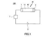
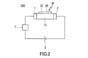
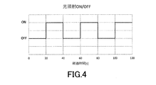
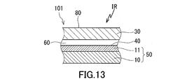
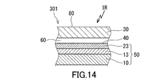
- the electrical resistance of the variable resistance unit 13 is such that if the major carrier of the variable resistance unit 13 and the carrier supplied from the carrier supply unit 23 are of the same type, that is, if both are electrons or both holes, infrared irradiation can be started. It will decrease due to the corresponding increase in major carriers.
- the electrical resistance of the variable resistance section 13 is infrared if the major carrier of the variable resistance section 13 and the carrier supplied from the carrier supply section 23 are different, that is, if one of the carriers is an electron and the other is a hole. Increased by carrier recombination upon initiation of irradiation.
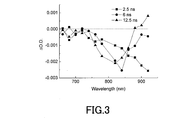
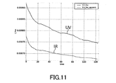
- the device according to the present embodiment has a relatively high sensitivity to irradiation of near infrared rays up to a wavelength of 2.5 ⁇ m, and may have a wavelength selectivity with a relatively low sensitivity for infrared rays having a wavelength longer than this.
- Such wavelength selectivity is an advantageous feature from the viewpoint of suppressing noise due to heat conduction.
- the measurement sample is blood and the infrared absorbing component is glucose.
- the measurement sample may be a part of a living body such as a fingertip or an earlobe.
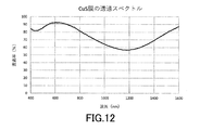
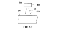
- the blood glucose level of blood can be calculated based on the absorption rate of infrared rays around 1500 nm, which can be transmitted through the living body and is characteristically absorbed by glucose, by the living body. That is, the infrared transmittance measuring device 500 can be used as a blood glucose level measuring device.
- This blood glucose level measuring device is a so-called non-invasive sensor, and is a sensor that takes advantage of the feature of the device 200 that it can handle molecules whose concentration and concentration distribution in the body change at high speed. This device can easily be a wearable sensor that takes advantage of the flexibility of the variable resistance unit 50.
- ruthenium oxide examples include those represented by RuO 2 or RuO 2-x (0 ⁇ x ⁇ 1). Similarly, rhenium oxide is represented by ReO 2 or ReO 2-x (0 ⁇ x ⁇ 1), and molybdenum oxide is represented by MoO 3 or MoO 3-x (0 ⁇ x ⁇ 1). As the tungsten oxide, those represented by WO 3 or WO 3-x (0 ⁇ x ⁇ 1) can be exemplified.
- a material capable of exhibiting such a long active carrier relaxation time after excitation of LSPR, regardless of the wavelength and intensity of pump light, is suitable as an LSPR-IR absorbent material.
- LSPR-IR absorbent material As the time-resolved transient absorption spectral method, a direct method for directly measuring the entire time of the phenomenon may be applied.
- the first ink contains copper sulfide nanoparticles and oleylamine, which is a compound that can coordinate with the copper sulfide nanoparticles.
- TGA thermogravimetric analysis
- the ratio of the mass of oleylamine to the total mass of copper sulfide nanoparticles and oleylamine was 10%. This ratio was the same in the subsequent examples.
Landscapes
- Physics & Mathematics (AREA)
- General Physics & Mathematics (AREA)
- Spectroscopy & Molecular Physics (AREA)
- Photometry And Measurement Of Optical Pulse Characteristics (AREA)
- Investigating Or Analysing Materials By Optical Means (AREA)
Priority Applications (4)
| Application Number | Priority Date | Filing Date | Title |
|---|---|---|---|
| EP21788628.2A EP4137789A4 (en) | 2020-04-13 | 2021-04-13 | INFRARED DETECTION DEVICE AND VARIABLE RESISTANCE FILM USING SAME |
| JP2022515403A JP7837020B2 (ja) | 2020-04-13 | 2021-04-13 | 赤外線センシングデバイス及びそれに用いる抵抗可変膜 |
| CN202180027792.XA CN116075700A (zh) | 2020-04-13 | 2021-04-13 | 红外线传感器件和用于该器件的电阻可变膜 |
| US17/996,046 US12276550B2 (en) | 2020-04-13 | 2021-04-13 | Infrared sensing device and variable resistance film included in the same |
Applications Claiming Priority (2)
| Application Number | Priority Date | Filing Date | Title |
|---|---|---|---|
| JP2020071711 | 2020-04-13 | ||
| JP2020-071711 | 2020-04-13 |
Publications (1)
| Publication Number | Publication Date |
|---|---|
| WO2021210593A1 true WO2021210593A1 (ja) | 2021-10-21 |
Family
ID=78085187
Family Applications (1)
| Application Number | Title | Priority Date | Filing Date |
|---|---|---|---|
| PCT/JP2021/015365 Ceased WO2021210593A1 (ja) | 2020-04-13 | 2021-04-13 | 赤外線センシングデバイス及びそれに用いる抵抗可変膜 |
Country Status (5)
| Country | Link |
|---|---|
| US (1) | US12276550B2 (https=) |
| EP (1) | EP4137789A4 (https=) |
| JP (1) | JP7837020B2 (https=) |
| CN (1) | CN116075700A (https=) |
| WO (1) | WO2021210593A1 (https=) |
Families Citing this family (1)
| Publication number | Priority date | Publication date | Assignee | Title |
|---|---|---|---|---|
| CN119805828B (zh) * | 2025-03-17 | 2025-07-15 | 中国人民解放军国防科技大学 | 一种光电耦合型lspr变红外发射率器件及其制备方法与应用 |
Citations (8)
| Publication number | Priority date | Publication date | Assignee | Title |
|---|---|---|---|---|
| JPH1062239A (ja) * | 1996-08-21 | 1998-03-06 | Mitsubishi Materials Corp | 赤外線検出素子 |
| JP2001013010A (ja) | 1999-06-28 | 2001-01-19 | Toyota Central Res & Dev Lab Inc | 抵抗変化型赤外線検出器 |
| JP2001183230A (ja) * | 1999-12-24 | 2001-07-06 | Kokusai Kiban Zairyo Kenkyusho:Kk | 光放射エネルギー強度測定装置 |
| JP2008139072A (ja) * | 2006-11-30 | 2008-06-19 | Nec Corp | 赤外線検知器及びその温度制御方法 |
| WO2016067905A1 (ja) * | 2014-10-30 | 2016-05-06 | 住友金属鉱山株式会社 | 熱線遮蔽粒子、熱線遮蔽粒子分散液、熱線遮蔽粒子分散体、熱線遮蔽粒子分散体合わせ透明基材、赤外線吸収透明基材、熱線遮蔽粒子の製造方法 |
| WO2018101446A1 (ja) * | 2016-12-02 | 2018-06-07 | 国立大学法人京都大学 | 光電変換機能を有する電子デバイス |
| JP2018524820A (ja) * | 2015-07-28 | 2018-08-30 | ネクスドット | 向上した性能を備える、ナノ結晶を利用した中遠赤外光検出器 |
| JP2019002852A (ja) * | 2017-06-16 | 2019-01-10 | 株式会社豊田中央研究所 | 電磁波検出器およびその製造方法 |
Family Cites Families (12)
| Publication number | Priority date | Publication date | Assignee | Title |
|---|---|---|---|---|
| JP2773730B2 (ja) * | 1996-03-07 | 1998-07-09 | 日本電気株式会社 | 光伝導型赤外線検出素子 |
| EP2072976A4 (en) * | 2006-10-11 | 2013-08-14 | Panasonic Corp | ELECTRONIC EQUIPMENT |
| JP2009175124A (ja) * | 2007-12-27 | 2009-08-06 | Rohm Co Ltd | プラズモン共鳴検出器 |
| JP2012164980A (ja) | 2011-01-21 | 2012-08-30 | Sumitomo Metal Mining Co Ltd | 光電変換装置とその製造方法 |
| EP2581721B1 (en) * | 2011-10-10 | 2019-05-08 | Samsung Electronics Co., Ltd | Infrared thermal detector and method of manufacturing the same |
| KR101922119B1 (ko) * | 2011-12-22 | 2019-02-14 | 삼성전자주식회사 | 적외선 검출기 및 이를 사용하는 적외선 검출 방법 |
| KR102040149B1 (ko) * | 2013-02-01 | 2019-11-04 | 삼성전자주식회사 | 적외선 검출기 |
| JP6172522B2 (ja) * | 2013-12-04 | 2017-08-02 | ソニー株式会社 | 赤外線検出素子およびその検出方法、並びに電子機器 |
| KR102227688B1 (ko) * | 2016-04-01 | 2021-03-15 | 스미토모 긴조쿠 고잔 가부시키가이샤 | 적외선 흡수 재료, 적외선 흡수 재료 분산액, 적외선 흡수 재료 분산체, 적외선 흡수 재료 분산체를 구비한 투명 기재 및 적외선 흡수 투명 기재 |
| JP7204667B2 (ja) * | 2017-04-20 | 2023-01-16 | トリナミクス ゲゼルシャフト ミット ベシュレンクテル ハフツング | 光検出器 |
| JP7232978B2 (ja) * | 2017-12-11 | 2023-03-06 | パナソニックIpマネジメント株式会社 | 赤外線センサおよび赤外線センサのボロメータ赤外線受光部を冷却する方法 |
| TWI679782B (zh) * | 2017-12-19 | 2019-12-11 | 財團法人工業技術研究院 | 感測裝置及其製造方法 |
-
2021
- 2021-04-13 JP JP2022515403A patent/JP7837020B2/ja active Active
- 2021-04-13 EP EP21788628.2A patent/EP4137789A4/en active Pending
- 2021-04-13 CN CN202180027792.XA patent/CN116075700A/zh active Pending
- 2021-04-13 US US17/996,046 patent/US12276550B2/en active Active
- 2021-04-13 WO PCT/JP2021/015365 patent/WO2021210593A1/ja not_active Ceased
Patent Citations (8)
| Publication number | Priority date | Publication date | Assignee | Title |
|---|---|---|---|---|
| JPH1062239A (ja) * | 1996-08-21 | 1998-03-06 | Mitsubishi Materials Corp | 赤外線検出素子 |
| JP2001013010A (ja) | 1999-06-28 | 2001-01-19 | Toyota Central Res & Dev Lab Inc | 抵抗変化型赤外線検出器 |
| JP2001183230A (ja) * | 1999-12-24 | 2001-07-06 | Kokusai Kiban Zairyo Kenkyusho:Kk | 光放射エネルギー強度測定装置 |
| JP2008139072A (ja) * | 2006-11-30 | 2008-06-19 | Nec Corp | 赤外線検知器及びその温度制御方法 |
| WO2016067905A1 (ja) * | 2014-10-30 | 2016-05-06 | 住友金属鉱山株式会社 | 熱線遮蔽粒子、熱線遮蔽粒子分散液、熱線遮蔽粒子分散体、熱線遮蔽粒子分散体合わせ透明基材、赤外線吸収透明基材、熱線遮蔽粒子の製造方法 |
| JP2018524820A (ja) * | 2015-07-28 | 2018-08-30 | ネクスドット | 向上した性能を備える、ナノ結晶を利用した中遠赤外光検出器 |
| WO2018101446A1 (ja) * | 2016-12-02 | 2018-06-07 | 国立大学法人京都大学 | 光電変換機能を有する電子デバイス |
| JP2019002852A (ja) * | 2017-06-16 | 2019-01-10 | 株式会社豊田中央研究所 | 電磁波検出器およびその製造方法 |
Non-Patent Citations (1)
| Title |
|---|
| See also references of EP4137789A4 |
Also Published As
| Publication number | Publication date |
|---|---|
| CN116075700A (zh) | 2023-05-05 |
| JP7837020B2 (ja) | 2026-03-30 |
| US12276550B2 (en) | 2025-04-15 |
| JPWO2021210593A1 (https=) | 2021-10-21 |
| EP4137789A1 (en) | 2023-02-22 |
| US20230184592A1 (en) | 2023-06-15 |
| EP4137789A4 (en) | 2023-10-11 |
Similar Documents
| Publication | Publication Date | Title |
|---|---|---|
| Tang et al. | Enabling low-drift flexible perovskite photodetectors by electrical modulation for wearable health monitoring and weak light imaging | |
| Samouco et al. | Laser-induced electrodes towards low-cost flexible UV ZnO sensors | |
| Pataniya et al. | based flexible photodetector functionalized by WSe2 nanodots | |
| Gogurla et al. | Multifunctional Au-ZnO plasmonic nanostructures for enhanced UV photodetector and room temperature NO sensing devices | |
| Rohizat et al. | Plasmon-enhanced reduced graphene oxide photodetector with monometallic of Au and Ag nanoparticles at VIS–NIR region | |
| Sturaro et al. | Degenerately doped metal oxide nanocrystals as plasmonic and chemoresistive gas sensors | |
| Gimenez et al. | ZnO− paper based photoconductive UV sensor | |
| Zhang et al. | Ultrasensitive photodetectors exploiting electrostatic trapping and percolation transport | |
| Cook et al. | Heat-assisted inkjet printing of tungsten oxide for high-performance ultraviolet photodetectors | |
| Yalagala et al. | ZnO nanowires based degradable high-performance photodetectors for eco-friendly green electronics | |
| Shi et al. | Split-ring structured all-inorganic perovskite photodetector arrays for masterly internet of things | |
| Bianchi et al. | Near infrared photothermoelectric effect in transparent AZO/ITO/Ag/ITO thin films | |
| Deng et al. | NIR-UV dual-mode photodetector with the assistance of machine-learning fabricated by hybrid laser processing | |
| Yuan et al. | High photosensitivity and low dark current of photoconductive semiconductor switch based on ZnO single nanobelt | |
| Xu et al. | Surface energy‐assisted patterning of vapor deposited all‐inorganic perovskite arrays for wearable optoelectronics | |
| Saimon et al. | Ag@ WO3 core–shell nanocomposite for wide range photo detection | |
| Mahana et al. | Photo-sensing characteristics of CuO thin films synthesized by thermal oxidation of Cu metal films | |
| WO2021210593A1 (ja) | 赤外線センシングデバイス及びそれに用いる抵抗可変膜 | |
| Tarwal et al. | Spray deposition of the nanostructured ZnO thin films for non-volatile resistive switching memory applications | |
| Sharma et al. | Quantum enhanced efficiency and spectral performance of paper-based flexible photodetectors functionalized with two dimensional materials | |
| US20230361235A1 (en) | Heat blocking device, heat blocking film, and heat blocking composition | |
| Wu et al. | A Self-Powered p-CuO/n-Si Heterojunction-Type Ultraviolet Photodetector | |
| CN104409555B (zh) | 一种基于石墨烯的紫外感应器及其制备方法 | |
| Villegas et al. | UV-response of aluminum-doped zinc oxide transparent films with different microstructures and electrical properties | |
| Li et al. | Printing ultrathin Quasi-2D Ga2O3 for fast yet highly responsive vertical photodetectors |
Legal Events
| Date | Code | Title | Description |
|---|---|---|---|
| 121 | Ep: the epo has been informed by wipo that ep was designated in this application |
Ref document number: 21788628 Country of ref document: EP Kind code of ref document: A1 |
|
| ENP | Entry into the national phase |
Ref document number: 2022515403 Country of ref document: JP Kind code of ref document: A |
|
| NENP | Non-entry into the national phase |
Ref country code: DE |
|
| ENP | Entry into the national phase |
Ref document number: 2021788628 Country of ref document: EP Effective date: 20221114 |
|
| WWG | Wipo information: grant in national office |
Ref document number: 17996046 Country of ref document: US |