WO2021209858A1 - 半導体装置 - Google Patents
半導体装置 Download PDFInfo
- Publication number
- WO2021209858A1 WO2021209858A1 PCT/IB2021/052826 IB2021052826W WO2021209858A1 WO 2021209858 A1 WO2021209858 A1 WO 2021209858A1 IB 2021052826 W IB2021052826 W IB 2021052826W WO 2021209858 A1 WO2021209858 A1 WO 2021209858A1
- Authority
- WO
- WIPO (PCT)
- Prior art keywords
- transistor
- oxide
- insulator
- semiconductor device
- conductor
- Prior art date
- Legal status (The legal status is an assumption and is not a legal conclusion. Google has not performed a legal analysis and makes no representation as to the accuracy of the status listed.)
- Ceased
Links
Images

























Classifications
-
- G—PHYSICS
- G11—INFORMATION STORAGE
- G11C—STATIC STORES
- G11C7/00—Arrangements for writing information into, or reading information out from, a digital store
- G11C7/16—Storage of analogue signals in digital stores using an arrangement comprising analogue/digital [A/D] converters, digital memories and digital/analogue [D/A] converters
-
- G—PHYSICS
- G06—COMPUTING OR CALCULATING; COUNTING
- G06N—COMPUTING ARRANGEMENTS BASED ON SPECIFIC COMPUTATIONAL MODELS
- G06N3/00—Computing arrangements based on biological models
- G06N3/02—Neural networks
- G06N3/04—Architecture, e.g. interconnection topology
- G06N3/0499—Feedforward networks
-
- G—PHYSICS
- G06—COMPUTING OR CALCULATING; COUNTING
- G06N—COMPUTING ARRANGEMENTS BASED ON SPECIFIC COMPUTATIONAL MODELS
- G06N3/00—Computing arrangements based on biological models
- G06N3/02—Neural networks
- G06N3/06—Physical realisation, i.e. hardware implementation of neural networks, neurons or parts of neurons
- G06N3/063—Physical realisation, i.e. hardware implementation of neural networks, neurons or parts of neurons using electronic means
-
- G—PHYSICS
- G11—INFORMATION STORAGE
- G11C—STATIC STORES
- G11C11/00—Digital stores characterised by the use of particular electric or magnetic storage elements; Storage elements therefor
- G11C11/21—Digital stores characterised by the use of particular electric or magnetic storage elements; Storage elements therefor using electric elements
- G11C11/34—Digital stores characterised by the use of particular electric or magnetic storage elements; Storage elements therefor using electric elements using semiconductor devices
- G11C11/40—Digital stores characterised by the use of particular electric or magnetic storage elements; Storage elements therefor using electric elements using semiconductor devices using transistors
-
- G—PHYSICS
- G11—INFORMATION STORAGE
- G11C—STATIC STORES
- G11C11/00—Digital stores characterised by the use of particular electric or magnetic storage elements; Storage elements therefor
- G11C11/21—Digital stores characterised by the use of particular electric or magnetic storage elements; Storage elements therefor using electric elements
- G11C11/34—Digital stores characterised by the use of particular electric or magnetic storage elements; Storage elements therefor using electric elements using semiconductor devices
- G11C11/40—Digital stores characterised by the use of particular electric or magnetic storage elements; Storage elements therefor using electric elements using semiconductor devices using transistors
- G11C11/401—Digital stores characterised by the use of particular electric or magnetic storage elements; Storage elements therefor using electric elements using semiconductor devices using transistors forming cells needing refreshing or charge regeneration, i.e. dynamic cells
- G11C11/402—Digital stores characterised by the use of particular electric or magnetic storage elements; Storage elements therefor using electric elements using semiconductor devices using transistors forming cells needing refreshing or charge regeneration, i.e. dynamic cells with charge regeneration individual to each memory cell, i.e. internal refresh
- G11C11/4023—Digital stores characterised by the use of particular electric or magnetic storage elements; Storage elements therefor using electric elements using semiconductor devices using transistors forming cells needing refreshing or charge regeneration, i.e. dynamic cells with charge regeneration individual to each memory cell, i.e. internal refresh using field effect transistors
-
- G—PHYSICS
- G11—INFORMATION STORAGE
- G11C—STATIC STORES
- G11C11/00—Digital stores characterised by the use of particular electric or magnetic storage elements; Storage elements therefor
- G11C11/21—Digital stores characterised by the use of particular electric or magnetic storage elements; Storage elements therefor using electric elements
- G11C11/34—Digital stores characterised by the use of particular electric or magnetic storage elements; Storage elements therefor using electric elements using semiconductor devices
- G11C11/40—Digital stores characterised by the use of particular electric or magnetic storage elements; Storage elements therefor using electric elements using semiconductor devices using transistors
- G11C11/401—Digital stores characterised by the use of particular electric or magnetic storage elements; Storage elements therefor using electric elements using semiconductor devices using transistors forming cells needing refreshing or charge regeneration, i.e. dynamic cells
- G11C11/403—Digital stores characterised by the use of particular electric or magnetic storage elements; Storage elements therefor using electric elements using semiconductor devices using transistors forming cells needing refreshing or charge regeneration, i.e. dynamic cells with charge regeneration common to a multiplicity of memory cells, i.e. external refresh
- G11C11/405—Digital stores characterised by the use of particular electric or magnetic storage elements; Storage elements therefor using electric elements using semiconductor devices using transistors forming cells needing refreshing or charge regeneration, i.e. dynamic cells with charge regeneration common to a multiplicity of memory cells, i.e. external refresh with three charge-transfer gates, e.g. MOS transistors, per cell
-
- G—PHYSICS
- G11—INFORMATION STORAGE
- G11C—STATIC STORES
- G11C27/00—Electric analogue stores, e.g. for storing instantaneous values
-
- G—PHYSICS
- G11—INFORMATION STORAGE
- G11C—STATIC STORES
- G11C27/00—Electric analogue stores, e.g. for storing instantaneous values
- G11C27/02—Sample-and-hold arrangements
-
- G—PHYSICS
- G11—INFORMATION STORAGE
- G11C—STATIC STORES
- G11C8/00—Arrangements for selecting an address in a digital store
- G11C8/16—Multiple access memory array, e.g. addressing one storage element via at least two independent addressing line groups
-
- H—ELECTRICITY
- H10—SEMICONDUCTOR DEVICES; ELECTRIC SOLID-STATE DEVICES NOT OTHERWISE PROVIDED FOR
- H10B—ELECTRONIC MEMORY DEVICES
- H10B12/00—Dynamic random access memory [DRAM] devices
- H10B12/30—DRAM devices comprising one-transistor - one-capacitor [1T-1C] memory cells
- H10B12/31—DRAM devices comprising one-transistor - one-capacitor [1T-1C] memory cells having a storage electrode stacked over the transistor
-
- H—ELECTRICITY
- H10—SEMICONDUCTOR DEVICES; ELECTRIC SOLID-STATE DEVICES NOT OTHERWISE PROVIDED FOR
- H10D—INORGANIC ELECTRIC SEMICONDUCTOR DEVICES
- H10D30/00—Field-effect transistors [FET]
- H10D30/60—Insulated-gate field-effect transistors [IGFET]
- H10D30/67—Thin-film transistors [TFT]
-
- G—PHYSICS
- G11—INFORMATION STORAGE
- G11C—STATIC STORES
- G11C11/00—Digital stores characterised by the use of particular electric or magnetic storage elements; Storage elements therefor
- G11C11/54—Digital stores characterised by the use of particular electric or magnetic storage elements; Storage elements therefor using elements simulating biological cells, e.g. neuron
-
- G—PHYSICS
- G11—INFORMATION STORAGE
- G11C—STATIC STORES
- G11C27/00—Electric analogue stores, e.g. for storing instantaneous values
- G11C27/005—Electric analogue stores, e.g. for storing instantaneous values with non-volatile charge storage, e.g. on floating gate or MNOS
-
- G—PHYSICS
- G11—INFORMATION STORAGE
- G11C—STATIC STORES
- G11C7/00—Arrangements for writing information into, or reading information out from, a digital store
- G11C7/04—Arrangements for writing information into, or reading information out from, a digital store with means for avoiding disturbances due to temperature effects
-
- H—ELECTRICITY
- H10—SEMICONDUCTOR DEVICES; ELECTRIC SOLID-STATE DEVICES NOT OTHERWISE PROVIDED FOR
- H10B—ELECTRONIC MEMORY DEVICES
- H10B12/00—Dynamic random access memory [DRAM] devices
-
- H—ELECTRICITY
- H10—SEMICONDUCTOR DEVICES; ELECTRIC SOLID-STATE DEVICES NOT OTHERWISE PROVIDED FOR
- H10B—ELECTRONIC MEMORY DEVICES
- H10B41/00—Electrically erasable-and-programmable ROM [EEPROM] devices comprising floating gates
- H10B41/70—Electrically erasable-and-programmable ROM [EEPROM] devices comprising floating gates the floating gate being an electrode shared by two or more components
-
- H—ELECTRICITY
- H10—SEMICONDUCTOR DEVICES; ELECTRIC SOLID-STATE DEVICES NOT OTHERWISE PROVIDED FOR
- H10D—INORGANIC ELECTRIC SEMICONDUCTOR DEVICES
- H10D30/00—Field-effect transistors [FET]
- H10D30/60—Insulated-gate field-effect transistors [IGFET]
- H10D30/67—Thin-film transistors [TFT]
- H10D30/6729—Thin-film transistors [TFT] characterised by the electrodes
- H10D30/673—Thin-film transistors [TFT] characterised by the electrodes characterised by the shapes, relative sizes or dispositions of the gate electrodes
- H10D30/6733—Multi-gate TFTs
- H10D30/6734—Multi-gate TFTs having gate electrodes arranged on both top and bottom sides of the channel, e.g. dual-gate TFTs
-
- H—ELECTRICITY
- H10—SEMICONDUCTOR DEVICES; ELECTRIC SOLID-STATE DEVICES NOT OTHERWISE PROVIDED FOR
- H10D—INORGANIC ELECTRIC SEMICONDUCTOR DEVICES
- H10D30/00—Field-effect transistors [FET]
- H10D30/60—Insulated-gate field-effect transistors [IGFET]
- H10D30/67—Thin-film transistors [TFT]
- H10D30/674—Thin-film transistors [TFT] characterised by the active materials
- H10D30/6755—Oxide semiconductors, e.g. zinc oxide, copper aluminium oxide or cadmium stannate
-
- H—ELECTRICITY
- H10—SEMICONDUCTOR DEVICES; ELECTRIC SOLID-STATE DEVICES NOT OTHERWISE PROVIDED FOR
- H10D—INORGANIC ELECTRIC SEMICONDUCTOR DEVICES
- H10D87/00—Integrated devices comprising both bulk components and either SOI or SOS components on the same substrate
Definitions
- One aspect of the present invention relates to a semiconductor device.
- One aspect of the present invention is not limited to the above technical fields.
- the technical field of the invention disclosed in the present specification and the like relates to a product, a method, or a manufacturing method.
- one aspect of the invention relates to a process, machine, manufacture, or composition of matter. Therefore, more specifically, the technical fields of one aspect of the present invention disclosed in the present specification include semiconductor devices, display devices, liquid crystal display devices, light emitting devices, power storage devices, imaging devices, storage devices, signal processing devices, and processors.
- Electronic devices, systems, their driving methods, their manufacturing methods, or their inspection methods can be mentioned as examples.
- CPUs central processing units
- GPUs graphics processing units
- storage devices and sensors
- sensors have been used in various electronic devices such as personal computers, smartphones, and digital cameras.
- the electronic components are being improved in various aspects such as miniaturization and low power consumption.
- Patent Document 1 and Patent Document 2 disclose a semiconductor device capable of writing and reading multi-valued data.
- transistors also referred to as "Si transistors” in which silicon is contained in the semiconductor layer on which channels are formed
- the elements are becoming finer as the process rules are reduced. Further, as the element becomes finer, the gate insulating film becomes thinner, so that the leakage current through the gate insulating film becomes a problem.
- One aspect of the present invention is to provide a semiconductor device capable of holding analog data. Alternatively, one aspect of the present invention is to provide a semiconductor device capable of accurately reading out the held analog data. Alternatively, one aspect of the present invention is to provide a semiconductor device having a reduced occupied area. Alternatively, one aspect of the present invention is to provide a semiconductor device with reduced power consumption. Alternatively, one aspect of the present invention is to provide a semiconductor device having a large storage capacity. Alternatively, one aspect of the present invention is to provide a highly reliable semiconductor device. Alternatively, one aspect of the present invention is to provide a novel semiconductor device.
- the problems of one aspect of the present invention are not limited to the problems listed above.
- the issues listed above do not preclude the existence of other issues.
- Other issues are issues not mentioned in this item, which are described below. Issues not mentioned in this item can be derived from descriptions in the description, drawings, etc. by those skilled in the art, and can be appropriately extracted from these descriptions.
- one aspect of the present invention solves at least one of the above-listed problems and other problems. It should be noted that one aspect of the present invention does not need to solve all of the above-listed problems and other problems.
- One aspect of the present invention is a semiconductor device that uses four transistors and two capacitive elements to form two holding circuits, two bootstrap circuits, and one source follower circuit.
- a storage node is provided in each of the two holding circuits, the data potential is written to one storage node, and the reference potential is written to the other storage node.
- one bootstrap circuit boosts the potential of one storage node and the other bootstrap circuit boosts the potential of the other storage node.
- the potential difference between the two storage nodes is output using the source follower circuit.
- the output impedance can be reduced by using the source follower circuit.
- Another aspect of the present invention is a semiconductor device having first to fifth circuits, the first circuit having a function of holding the first potential, and the second circuit boosting the first potential.
- the third circuit has a function of holding a second potential
- the fourth circuit has a function of boosting the second potential
- the fifth circuit has a boosted first potential and boosting. It is a semiconductor device having a function of outputting a third potential corresponding to the potential difference of the second potential.
- the above-mentioned semiconductor device may include, for example, first to fourth transistors, a first capacitance element, and a second capacitance element.
- the first circuit includes the first transistor and the first capacitance element
- the second circuit includes the second transistor and the first capacitance element
- the third circuit includes the third transistor and the third transistor.
- a second capacitive element may be included
- the fourth circuit may include a fourth transistor and a second capacitive element
- the fifth circuit may include a second transistor and a fourth transistor.
- Another aspect of the present invention includes first to fourth transistors, a first capacitive element, and a second capacitive element, and one of the source and drain of the first transistor is electrically connected to the first terminal.
- the other of the source or drain of the first transistor is electrically connected to the gate of the second transistor, the gate of the first transistor is electrically connected to the second terminal, and the source or drain of the third transistor.
- One of the drains is electrically connected to the third terminal, the other of the source or drain of the third transistor is electrically connected to the gate of the fourth transistor, and the gate of the third transistor is electrically connected to the fourth terminal.
- One of the source or drain of the second transistor is electrically connected to the fifth terminal, and the other of the source or drain of the second transistor is electrically connected to the seventh terminal.
- One of the source or drain of the fourth transistor is electrically connected to the sixth terminal, the other of the source or drain of the fourth transistor is electrically connected to the seventh terminal, and one electrode of the first capacitance element is the first. Electrically connected to the gate of the two transistors, the other electrode of the first capacitive element is electrically connected to the seventh terminal, and one electrode of the second capacitive element is electrically connected to the gate of the fourth transistor.
- the other electrode of the second capacitive element that is connected is a semiconductor device that is electrically connected to the seventh terminal.
- the third terminal and the sixth terminal may be electrically connected.
- the first transistor and the third transistor preferably contain an oxide semiconductor in the semiconductor layer on which the channel is formed.
- the second transistor and the fourth transistor preferably contain an oxide semiconductor in the semiconductor layer on which the channel is formed.
- the oxide semiconductor preferably contains at least one of indium and zinc.
- a semiconductor device capable of holding analog data.
- a semiconductor device capable of accurately reading the held analog data.
- a semiconductor device having a reduced occupied area it is possible to provide a semiconductor device with reduced power consumption.
- a semiconductor device having a large storage capacity can be provided.
- a highly reliable semiconductor device can be provided.
- a new semiconductor device can be provided.
- the effects of one aspect of the present invention are not limited to the effects listed above.
- the effects listed above do not preclude the existence of other effects.
- the other effects are the effects not mentioned in this item, which are described below. Effects not mentioned in this item can be derived from those described in the description, drawings, etc. by those skilled in the art, and can be appropriately extracted from these descriptions.
- one aspect of the present invention has at least one of the above-listed effects and other effects. Therefore, one aspect of the present invention may not have the effects listed above.
- FIG. 1A and 1B are circuit diagrams of a semiconductor device according to an aspect of the present invention.
- 2A and 2B are circuit diagrams of a semiconductor device according to an aspect of the present invention.
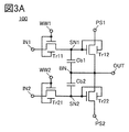
- 3A and 3B are circuit diagrams of a semiconductor device according to an aspect of the present invention.
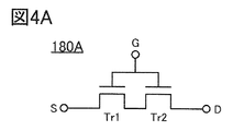
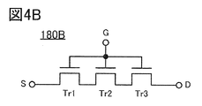
- 4A and 4B are diagrams showing circuit symbols of transistors.
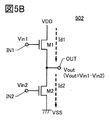
- 5A and 5B are diagrams illustrating a source follower circuit.
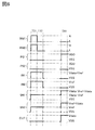
- FIG. 6 is a timing chart illustrating an operation example of the semiconductor device.
- 7A and 7B are diagrams for explaining an operation example of the semiconductor device.
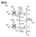
- 8A and 8B are diagrams for explaining an operation example of the semiconductor device.
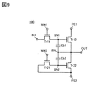
- FIG. 9 is a circuit diagram of a semiconductor device according to one aspect of the present invention.
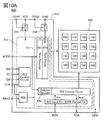
- FIG. 10A is a block diagram illustrating a configuration example of the semiconductor device.
- FIG. 10B is a perspective view of the semiconductor device.
- FIG. 11 is a block diagram illustrating a CPU.
- 12A and 12B are perspective views of the semiconductor device.
- 13A and 13B are perspective views of the semiconductor device.
- 14A and 14B are perspective views of the semiconductor device.
- 15A and 15B are diagrams for explaining a configuration example of a neural network.
- FIG. 16 is a diagram showing a structural example of the semiconductor device.
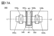
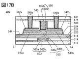
- 17A to 17C are diagrams showing a configuration example of a transistor.
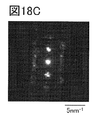
- FIG. 18A is a diagram for explaining the classification of the crystal structure of IGZO
- FIG. 18B is a diagram for explaining the XRD spectrum of crystalline IGZO
- FIG. 18A is a diagram for explaining the classification of the crystal structure of IGZO
- FIG. 18B is a diagram for explaining the XRD spectrum of crystalline IGZO
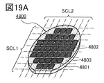
- FIG. 19B is a perspective view showing an example of a chip
- FIGS. 19C and 19D are perspective views showing an example of an electronic component.
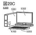
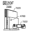
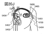
- 20A to 20J are diagrams for explaining an example of an electronic device.
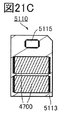
- 21A to 21E are diagrams illustrating an example of an electronic device.
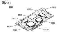
- 22A to 22C are diagrams illustrating an example of an electronic device.
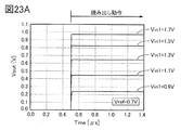
- 23A and 23B are diagrams according to an embodiment.
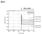
- FIG. 24 is a diagram according to an embodiment.
- FIG. 25 is a diagram according to an embodiment.
- the semiconductor device is a device utilizing semiconductor characteristics, and refers to a circuit including a semiconductor element (transistor, diode, photodiode, etc.), a device having the same circuit, and the like. It also refers to all devices that can function by utilizing semiconductor characteristics. For example, an integrated circuit, a chip having an integrated circuit, or an electronic component in which the chip is housed in a package is an example of a semiconductor device. Further, the storage device, the display device, the light emitting device, the lighting device, the electronic device, and the like are themselves semiconductor devices, and may have the semiconductor device.
- an element for example, a switch, a transistor, a capacitive element, an inductor, a resistance element, a diode, a display
- One or more devices, light emitting devices, loads, etc. can be connected between X and Y.
- the switch has a function of controlling the on state and the off state. That is, the switch is in a conducting state (on state) or a non-conducting state (off state), and has a function of controlling whether or not a current flows.
- a circuit that enables functional connection between X and Y for example, a logic circuit (inverter, NAND circuit, NOR circuit, etc.), signal conversion, etc.) Circuits (digital-analog conversion circuit, analog-digital conversion circuit, gamma correction circuit, etc.), potential level conversion circuit (power supply circuit (boost circuit, step-down circuit, etc.), level shifter circuit that changes the signal potential level, etc.), voltage source, current source , Switching circuit, amplifier circuit (circuit that can increase signal amplitude or current amount, operational amplifier, differential amplifier circuit, source follower circuit, buffer circuit, etc.), signal generation circuit, storage circuit, control circuit, etc.) It is possible to connect one or more to and from. As an example, even if another circuit is sandwiched between X and Y, if the signal output from X is transmitted to Y, it is assumed that X and Y are functionally connected. do.
- X and Y are electrically connected, it means that X and Y are electrically connected (that is, another element between X and Y). Or when they are connected with another circuit in between) and when X and Y are directly connected (that is, they are connected without another element or another circuit between X and Y). If there is) and.
- X and Y, the source (or the first terminal, etc.) and the drain (or the second terminal, etc.) of the transistor are electrically connected to each other, and the X, the source (or the second terminal, etc.) of the transistor are connected to each other. (1 terminal, etc.), the drain of the transistor (or the 2nd terminal, etc.), and Y are electrically connected in this order.
- the source of the transistor (or the first terminal, etc.) is electrically connected to X
- the drain of the transistor (or the second terminal, etc.) is electrically connected to Y
- the X, the source of the transistor (such as the second terminal).
- the first terminal, etc.), the drain of the transistor (or the second terminal, etc.), and Y are electrically connected in this order.
- X is electrically connected to Y via the source (or first terminal, etc.) and drain (or second terminal, etc.) of the transistor, and X, the source (or first terminal, etc.) of the transistor. (Terminals, etc.), transistor drains (or second terminals, etc.), and Y are provided in this connection order.
- the source (or first terminal, etc.) and drain (or second terminal, etc.) of the transistor can be separated. Separately, the technical scope can be determined. Note that these expression methods are examples, and are not limited to these expression methods.
- X and Y are assumed to be objects (for example, devices, elements, circuits, wirings, electrodes, terminals, conductive films, layers, etc.).
- circuit diagram shows that the independent components are electrically connected to each other, one component has the functions of a plurality of components.
- one component has the functions of a plurality of components.
- the term "electrically connected” as used herein includes the case where one conductive film has the functions of a plurality of components in combination.
- the “resistance element” can be, for example, a circuit element having a resistance value higher than 0 ⁇ , wiring, or the like. Therefore, in the present specification and the like, the “resistive element” includes a wiring having a resistance value, a transistor in which a current flows between a source and a drain, a diode, a coil, and the like. Therefore, the term “resistor element” can be paraphrased into terms such as “resistance”, “load”, and “region having resistance value”, and conversely, the terms “resistance”, “load”, and “region having resistance value” are used. , “Resistance element” and so on.
- the resistance value can be, for example, preferably 1 m ⁇ or more and 10 ⁇ or less, more preferably 5 m ⁇ or more and 5 ⁇ or less, and further preferably 10 m ⁇ or more and 1 ⁇ or less. Further, for example, it may be 1 ⁇ or more and 1 ⁇ 10 9 ⁇ or less.
- the “capacitance element” means, for example, a circuit element having a capacitance value higher than 0F, a wiring region having a capacitance value, a parasitic capacitance, a transistor gate capacitance, and the like. Can be. Therefore, in the present specification and the like, the “capacitive element” is not only a circuit element containing a pair of electrodes and a dielectric contained between the electrodes, but also a parasitic element appearing between the wirings. It shall include the capacitance, the gate capacitance that appears between the gate and one of the source or drain of the transistor, and so on.
- capacitor element in addition, terms such as “capacitive element”, “parasitic capacitance”, and “gate capacitance” can be paraphrased into terms such as “capacity”, and conversely, the term “capacity” refers to “capacitive element”, “parasitic capacitance”, and “capacity”. It can be paraphrased into terms such as “gate capacitance”.
- the term “pair of electrodes” of “capacity” can be paraphrased as “pair of conductors", “pair of conductive regions", “pair of regions” and the like.
- the value of the capacitance can be, for example, 0.05 fF or more and 10 pF or less. Further, for example, it may be 1 pF or more and 10 ⁇ F or less.
- the transistor has three terminals called a gate, a source, and a drain.
- the gate is a control terminal that controls the conduction state of the transistor.
- the two terminals that function as sources or drains are the input and output terminals of the transistor.
- One of the two input / output terminals becomes a source and the other becomes a drain depending on the high and low potentials given to the conductive type (n-channel type, p-channel type) of the transistor and the three terminals of the transistor. Therefore, in the present specification and the like, the terms source and drain can be paraphrased with each other.
- the transistor when explaining the connection relationship of transistors, "one of the source or drain” (or the first electrode or the first terminal), “the other of the source or drain” (or the second electrode, or The notation (second terminal) is used.
- it may have a back gate in addition to the above-mentioned three terminals.
- one of the gate or the back gate of the transistor may be referred to as a first gate
- the other of the gate or the back gate of the transistor may be referred to as a second gate.
- the terms “gate” and “backgate” may be interchangeable.
- the respective gates When the transistor has three or more gates, the respective gates may be referred to as a first gate, a second gate, a third gate, and the like in the present specification and the like.
- the “on current” may mean a current flowing between the source and the drain when the transistor is in the on state.
- the “off current” may mean a current flowing between the source and the drain when the transistor is in the off state.
- a node can be paraphrased as a terminal, a wiring, an electrode, a conductive layer, a conductor, an impurity region, or the like, depending on a circuit configuration and / or a device structure or the like.
- terminals, wiring, etc. can be paraphrased as nodes.
- ground potential ground potential
- the potentials are relative, and when the reference potential changes, the potential given to the wiring, the potential applied to the circuit or the like, the potential output from the circuit or the like also changes.
- the high power supply potential VDD (hereinafter, also simply referred to as “VDD”) indicates a power supply potential having a potential higher than that of the low power supply potential VSS (hereinafter, also simply referred to as “VSS”). Further, VSS indicates a power supply potential having a potential lower than VDD. Further, the ground potential (hereinafter, also simply referred to as “GND”) can be used as VDD or VSS. For example, when VDD is the ground potential, VSS is a potential lower than the ground potential, and when VSS is the ground potential, VDD is a potential higher than the ground potential.
- the "current” is a charge transfer phenomenon (electrical conduction).
- the description “electrical conduction of a positively charged body is occurring” means “electrical conduction of a negatively charged body in the opposite direction”. Is happening. " Therefore, in the present specification and the like, “current” refers to a charge transfer phenomenon (electrical conduction) accompanying the movement of carriers, unless otherwise specified.
- the carrier here include electrons, holes, anions, cations, complex ions, and the like, and the carriers differ depending on the system in which the current flows (for example, semiconductor, metal, electrolytic solution, vacuum, etc.).
- the "current direction” in the wiring or the like shall be the direction in which the positive carrier moves, and shall be described as a positive current amount.
- the direction in which the negative carrier moves is opposite to the direction of the current, and is expressed by the amount of negative current. Therefore, in the present specification and the like, if there is no notice about the positive or negative of the current (or the direction of the current), the description such as “current flows from element A to element B” means “current flows from element B to element A” or the like. It can be paraphrased as. Further, the description such as “a current is input to the element A” can be rephrased as "a current is output from the element A” or the like.
- the ordinal numbers “first”, “second”, and “third” are added to avoid confusion of the components. Therefore, the number of components is not limited. Moreover, the order of the components is not limited. For example, the component referred to in “first” in one of the embodiments of the present specification and the like may be the component referred to in “second” in another embodiment or in the claims. There can also be. Further, for example, the component mentioned in “first” in one of the embodiments of the present specification and the like may be omitted in another embodiment or in the claims.
- the terms “upper” and “lower” do not limit the positional relationship of the components to be directly above or directly below and to be in direct contact with each other.
- the terms “electrode B on the insulating layer A” it is not necessary that the electrode B is formed in direct contact with the insulating layer A, and another configuration is formed between the insulating layer A and the electrode B. Do not exclude those that contain elements.
- the positional relationship of the constituent elements changes as appropriate according to the direction in which each configuration is depicted. Therefore, it is not limited to the words and phrases explained in the specification and the like, and can be appropriately paraphrased according to the situation.
- terms indicating the arrangement such as “above” and “below” may be used for convenience in order to explain the positional relationship of the components with reference to the drawings. Therefore, in the expression of "insulator located on the upper surface of the conductor”, it can be rephrased as “insulator located on the lower surface of the conductor” by rotating the direction of the drawing shown by 180 degrees. Further, in the expression of "insulator located on the upper surface of the conductor”, it can be paraphrased as "insulator located on the left side (or right side) of the conductor” by rotating the direction of the drawing shown by 90 degrees. can.
- electrode B overlapping the insulating layer A is not limited to the state of "the electrode B is formed on the insulating layer A", but “the electrode B is formed under the insulating layer A”. It does not exclude the state of "being” or the state of "the electrode B is formed on the right side (or left side) of the insulating layer A”.
- the terms “adjacent” and “proximity” do not limit that the components are in direct contact with each other.
- electrode B adjacent to the insulating layer A it is not necessary that the insulating layer A and the electrode B are formed in direct contact with each other, and another component is formed between the insulating layer A and the electrode B. Do not exclude those that include.
- membrane and layer can be interchanged with each other depending on the situation.
- Electrode may be used as part of a “wiring” and vice versa.
- the terms “electrode” and “wiring” include the case where a plurality of “electrodes” and “wiring” are integrally formed.
- a “terminal” may be used as part of a “wiring” and an “electrode” and vice versa.
- the term “terminal” includes a case where a plurality of "electrodes", “wiring”, “terminals” and the like are integrally formed.
- the "electrode” can be a part of the “wiring” or the “terminal”, and for example, the “terminal” can be a part of the “wiring” or the “electrode”.
- terms such as “electrode”, “wiring”, and “terminal” may be replaced with terms such as "area” in some cases.
- wiring can be interchanged with each other in some cases or depending on the situation.
- “wiring”. It may be possible to change the term to the term “signal line”. Further, for example, it may be possible to change the term “wiring” to a term such as “power line”. The reverse is also true, and it may be possible to change terms such as “signal line” and “power supply line” to the term “wiring”.
- a term such as “power line” may be changed to a term such as "signal line”.
- terms such as “signal line” may be changed to terms such as "power line”.
- the term “potential” applied to the wiring may be changed to a term such as “signal” in some cases or depending on the situation. The reverse is also true, and terms such as “signal” may be changed to the term “potential”.
- semiconductor impurities refer to, for example, components other than the main components constituting the semiconductor layer.
- an element having a concentration of less than 0.1 atomic% is an impurity.
- the inclusion of impurities may result in, for example, an increase in the defect level density of the semiconductor, a decrease in carrier mobility, a decrease in crystallinity, and the like.
- the impurities that change the characteristics of the semiconductor include, for example, group 1 element, group 2 element, group 13 element, group 14 element, group 15 element, and other than the main component.
- transition metals and the like and in particular, hydrogen (also contained in water), lithium, sodium, silicon, boron, phosphorus, carbon, nitrogen and the like.
- the impurities that change the characteristics of the semiconductor include, for example, Group 1 elements other than oxygen and hydrogen, Group 2 elements, Group 13 elements, Group 15 elements, and the like. be.
- the switch means a switch that is in a conductive state (on state) or a non-conducting state (off state) and has a function of controlling whether or not a current flows.
- the switch means a switch having a function of selecting and switching a path through which a current flows.
- an electric switch, a mechanical switch, or the like can be used. That is, the switch is not limited to a specific switch as long as it can control the current.
- Examples of electrical switches include transistors (for example, bipolar transistors, MOS transistors, etc.), diodes (for example, PN diodes, PIN diodes, Schottky diodes, MIM (Metal Insulator Metal) diodes, and MIS (Metal Insulator Semiconductor) diodes. , Diode-connected transistors, etc.), or logic circuits that combine these.
- transistors for example, bipolar transistors, MOS transistors, etc.
- diodes for example, PN diodes, PIN diodes, Schottky diodes, MIM (Metal Insulator Metal) diodes, and MIS (Metal Insulator Semiconductor) diodes. , Diode-connected transistors, etc.
- the "conducting state (on state)" of the transistor means a state in which the source and drain of the transistor can be regarded as being electrically short-circuited.
- the "non-conducting state (off state)" of the transistor means a state in which the source and drain of the transistor can be regarded as being electrically cut off.
- the polarity (conductive type) of the transistor is not particularly limited.
- a mechanical switch is a switch using MEMS (Micro Electro Mechanical System) technology.
- the switch has an electrode that can be moved mechanically, and the movement of the electrode controls conduction and non-conduction.
- parallel means a state in which two straight lines are arranged at an angle of ⁇ 10 ° or more and 10 ° or less. Therefore, the case of ⁇ 5 ° or more and 5 ° or less is also included.
- substantially parallel or approximately parallel means a state in which two straight lines are arranged at an angle of ⁇ 30 ° or more and 30 ° or less.
- vertical means a state in which two straight lines are arranged at an angle of 80 ° or more and 100 ° or less. Therefore, the case of 85 ° or more and 95 ° or less is also included.
- substantially vertical or “approximately vertical” means a state in which two straight lines are arranged at an angle of 60 ° or more and 120 ° or less.
- a metal oxide is a metal oxide in a broad sense. Metal oxides are classified into oxide insulators, oxide conductors (including transparent oxide conductors), oxide semiconductors (also referred to as Oxide Semiconductor or simply OS) and the like. For example, when a metal oxide is used in the active layer of a transistor, the metal oxide may be referred to as an oxide semiconductor. That is, when a metal oxide can form a channel forming region of a transistor having at least one of an amplification action, a rectifying action, and a switching action, the metal oxide is referred to as a metal oxide semiconductor. be able to. Further, when describing as an OS transistor, it can be paraphrased as a transistor having a metal oxide or an oxide semiconductor.
- a metal oxide having nitrogen may also be collectively referred to as a metal oxide. Further, a metal oxide having nitrogen may be referred to as a metal oxynitride.
- the configuration shown in each embodiment can be appropriately combined with the configuration shown in other embodiments to form one aspect of the present invention. Further, when a plurality of configuration examples are shown in one embodiment, the configuration examples can be appropriately combined with each other.
- the content (may be a part of the content) described in one embodiment is the other content (may be a part of the content) described in the embodiment and one or more other implementations. It is possible to apply, combine, or replace at least one content with the content described in the form of (may be a part of the content).
- figure (which may be a part) described in one embodiment is different from another part of the figure, another figure (which may be a part) described in the embodiment, and one or more other figures.
- the figure (which may be a part) described in the embodiment is different from another part of the figure, another figure (which may be a part) described in the embodiment, and one or more other figures.
- more figures can be formed.
- the components are classified according to their functions and shown as blocks independent of each other.
- it is difficult to separate the components for each function and there may be a case where a plurality of functions are involved in one circuit or a case where one function is involved in a plurality of circuits. Therefore, the blocks in the block diagram are not limited to the components described in the specification, and can be appropriately paraphrased according to the situation.
- the size, layer thickness, or area may be exaggerated for clarity. Therefore, it is not necessarily limited to its size and aspect ratio.
- the drawings schematically show ideal examples, and are not limited to the shapes or values shown in the drawings. For example, it is possible to include variations in the signal, voltage, or current due to noise, or variations in the signal, voltage, or current due to timing lag.
- the code is used for identification such as "_1", “[n]", “[m, n]”. May be added and described.
- one of the two wiring GLs may be described as wiring GL [1], and the other may be described as wiring GL [2] or the like.
- FIG. 1A shows a circuit diagram of the semiconductor device 100 according to one aspect of the present invention.
- the semiconductor device 100 can function as a storage circuit capable of holding analog data. Further, the semiconductor device 100 can function as a storage element capable of holding analog data.
- the semiconductor device 100 includes a transistor Tr11, a transistor Tr12, a transistor Tr21, a transistor Tr22, a capacitive element Cb1, and a capacitive element Cb2.
- the semiconductor device 100 includes a holding circuit 110a, a holding circuit 110b, a bootstrap circuit 120a, a bootstrap circuit 120b, and a source follower circuit 130.
- the holding circuit 110a includes a transistor Tr11 and a capacitance element Cb1, and the holding circuit 110b includes a transistor Tr21 and a capacitance element Cb2.
- the bootstrap circuit 120a includes a transistor Tr12 and a capacitive element Cb1, and the bootstrap circuit 120b includes a transistor Tr22 and a capacitive element Cb2.
- the source follower circuit 130 includes a transistor Tr12 and a transistor Tr22.
- the gate of the transistor Tr11 is electrically connected to the terminal WW1, one of the source or drain of the transistor Tr11 is electrically connected to the terminal IN1, and the other is electrically connected to the gate of the transistor Tr12.
- One of the source or drain of the transistor Tr12 is electrically connected to the terminal PS1 and the other is electrically connected to the terminal OUT.
- the gate of the transistor Tr21 is electrically connected to the terminal WW2, one of the source or drain of the transistor Tr21 is electrically connected to the terminal IN2, and the other is electrically connected to the gate of the transistor Tr22.
- One of the source or drain of the transistor Tr22 is electrically connected to the terminal OUT, and the other is electrically connected to the terminal PS2.
- One electrode constituting the capacitive element Cb1 is electrically connected to the gate of the transistor Tr12, and the other electrode is electrically connected to the terminal OUT.
- One electrode constituting the capacitive element Cb2 is electrically connected to the terminal OUT, and the other electrode is electrically connected to the gate of the transistor Tr22.
- the node where the source or drain of the transistor Tr11, the gate of the transistor Tr12, and one of the electrodes constituting the capacitive element Cb1 are electrically connected functions as the node SN1.
- the node at which the source or drain of the transistor Tr21, the gate of the transistor Tr22, and the other electrode constituting the capacitive element Cb2 are electrically connected functions as the node SN2.
- the other electrode constituting the capacitance element Cb1, one electrode constituting the capacitance element Cb2, and the node electrically connected to the terminal OUT function as a node BN.
- the node SN1 and the node SN2 each function as a storage node.
- the holding circuit 110a has a function of holding the potential (charge) written in the node SN1 via the transistor Tr11.
- the holding circuit 110b has a function of holding the potential (charge) written in the node SN2 via the transistor Tr21.
- a potential for turning on the transistor Tr11 is supplied to the gate of the transistor Tr11, and an electric charge for making the node SN1 a predetermined potential is supplied to the node SN1 via the source and drain of the transistor Tr11. .. After that, a potential for turning off the transistor Tr11 is supplied to the gate of the transistor Tr11. By turning off the transistor Tr11, the electric charge written to the node SN1 is retained.
- a potential for turning on the transistor Tr21 is supplied to the gate of the transistor Tr21, and an electric charge for bringing the node SN2 to a predetermined potential is supplied to the node SN2 via the source and drain of the transistor Tr21. After that, a potential for turning off the transistor Tr21 is supplied to the gate of the transistor Tr21. By turning off the transistor Tr21, the electric charge written to the node SN2 is retained. Therefore, node SN1 and node SN2 are also referred to as "holding nodes”. Further, the transistor Tr11 and the transistor Tr21 are also referred to as "writing transistors”.
- a single crystal semiconductor, a polycrystalline semiconductor, a microcrystal semiconductor, an amorphous semiconductor, or the like can be used alone or in combination.
- the semiconductor material for example, silicon, germanium, or the like can be used. Further, compound semiconductors such as silicon germanium, silicon carbide, gallium arsenide, oxide semiconductors, and nitride semiconductors may be used.
- the semiconductor layer used for the transistor may be a stack of a plurality of semiconductor layers.
- semiconductors having different crystal states may be used, or different semiconductor materials may be used.
- the transistor Tr11 and the transistor Tr21 are preferably transistors (also referred to as "OS transistors") containing an oxide semiconductor in the semiconductor layer on which the channel is formed. Since the oxide semiconductor has a band gap of 2 eV or more, the off-current is remarkably small.
- OS transistors also referred to as "OS transistors”
- the electric charge written in the holding node can be held for a long period of time.
- the semiconductor device 100 can be called an "OS memory".
- the OS memory can retain the written information for a period of one year or more, or even ten years or more, even if the power supply is stopped. Therefore, the OS memory can be regarded as a non-volatile memory.
- the OS memory can hold not only binary information (1 bit) but also multi-value (multi-bit) information.
- the OS memory is a method of writing an electric charge to a node via an OS transistor, a high voltage required for a conventional flash memory is not required, and a high-speed writing operation can be realized. Further, the erasing operation before data rewriting performed in the flash memory is unnecessary in the OS memory. Also, since no charge is injected or withdrawn into the floating gate or charge capture layer, the OS memory can write and read data virtually unlimited times. The OS memory has less deterioration than the conventional flash memory, and high reliability can be obtained.
- the OS memory does not undergo a structural change at the atomic level like a magnetoresistive memory (MRAM) or a resistance change type memory (ReRAM). Therefore, the OS memory is superior in rewrite resistance to the magnetoresistive memory and the resistance change type memory.
- MRAM magnetoresistive memory
- ReRAM resistance change type memory
- the off-current of the OS transistor hardly increases even in a high temperature environment. Specifically, the off-current hardly increases even at an environmental temperature of room temperature or higher and 200 ° C. or lower. In addition, the on-current does not easily decrease even in a high temperature environment.
- the storage device including the OS memory has stable operation even in a high temperature environment, and high reliability can be obtained.
- the OS transistor has a high dielectric strength between the source and the drain. By using an OS transistor as a transistor constituting a semiconductor device, operation is stable even in a high temperature environment, and a semiconductor device with good reliability can be realized. Therefore, it is preferable to use an OS transistor for the transistor Tr11, the transistor Tr21, the transistor Tr12, and the transistor Tr22.
- the gate insulating film of the transistor Tr12 and the transistor Tr22 is extremely thin, the electric charge written to the node SN1 and the node SN2 may leak through the gate insulating film (also referred to as “gate leak”).
- the thickness of the gate insulating film of the transistor Tr12 and the transistor Tr22 is preferably about the same as the thickness of the gate insulating film of the transistor Tr11 and the transistor Tr21.
- an OS transistor may be used for the transistor Tr11 and the transistor Tr21
- a Si transistor may be used for the transistor Tr12 and the transistor Tr22.
- the Si transistor used for the transistor Tr12 and the transistor Tr22 a Si transistor having a structure with less gate leakage may be used.
- the data read speed can be increased by using the Si transistor for the transistor Tr12 and the transistor Tr22.
- the gate of the transistor Tr11 and the gate of the transistor Tr21 may be electrically connected to the wiring WWL.
- FIG. 2A shows an example in which the back gate of the transistor Tr12 is electrically connected to the terminal BG14 and the back gate of the transistor Tr22 is electrically connected to the terminal BG24.
- the threshold voltage of the transistor Tr12 can be changed.
- the threshold voltage of the transistor Tr22 can be changed.
- FIG. 2B shows an example in which the back gate of the transistor Tr11 is electrically connected to the terminal BG13 and the back gate of the transistor Tr21 is electrically connected to the terminal BG23.
- the threshold voltage of the transistor Tr11 can be changed.
- the threshold voltage of the transistor Tr21 can be changed.
- FIG. 3A shows an example in which a gate and a back gate are electrically connected in each of the transistor Tr11, the transistor Tr12, the transistor Tr21, and the transistor Tr22.
- FIG. 3B shows an example in which the back gate of the transistor Tr22 is electrically connected to the other of the source or drain of the transistor Tr22.
- each of the transistor Tr11, the transistor Tr12, the transistor Tr21, and the transistor Tr22 may be a double-gate type transistor.
- FIG. 4A shows an example of a circuit symbol of the double gate type transistor 180A.
- the transistor 180A has a configuration in which the transistor Tr1 and the transistor Tr2 are connected in series.
- one of the source or drain of the transistor Tr1 is electrically connected to the terminal S
- the other of the source or drain of the transistor Tr1 is electrically connected to one of the source or drain of the transistor Tr2, and the source of the transistor Tr2.
- the other side of the drain is electrically connected to the terminal D.
- FIG. 4A shows a state in which the gates of the transistor Tr1 and the transistor Tr2 are electrically connected and are electrically connected to the terminal G.
- the transistor 180A shown in FIG. 4A has a function of switching between the terminal S and the terminal D in a conductive state or a non-conducting state by changing the potential of the terminal G. Therefore, the transistor 180A, which is a double-gate type transistor, contains the transistor Tr1 and the transistor Tr2 and functions as one transistor. That is, in FIG. 4A, one of the source or drain of the transistor 180A is electrically connected to the terminal S, the other of the source or drain is electrically connected to the terminal D, and the gate is electrically connected to the terminal G. It can be said that there is.
- each of the transistor Tr11, the transistor Tr12, the transistor Tr21, and the transistor Tr22 may be a triple gate type transistor.
- FIG. 4B shows an example of a circuit symbol of the triple gate type transistor 180B.
- the transistor 180B has a configuration in which a transistor Tr1, a transistor Tr2, and a transistor Tr3 are connected in series.
- one of the source or drain of the transistor Tr1 is electrically connected to the terminal S
- the other of the source or drain of the transistor Tr1 is electrically connected to one of the source or drain of the transistor Tr2, and the source of the transistor Tr2.
- the other of the drains is electrically connected to one of the source or drain of the transistor Tr3, and the other of the source or drain of the transistor Tr3 is electrically connected to the terminal D.
- FIG. 4B shows a state in which the gates of the transistor Tr1, the transistor Tr2, and the transistor Tr3 are electrically connected and electrically connected to the terminal G.
- the transistor 180B shown in FIG. 4B has a function of switching between the terminal S and the terminal D in a conductive state or a non-conducting state by changing the potential of the terminal G. Therefore, the transistor 180B, which is a triple-gate type transistor, contains the transistor Tr1, the transistor Tr2, and the transistor Tr3, and functions as one transistor. That is, in FIG. 4B, one of the source or drain of the transistor 180B is electrically connected to the terminal S, the other of the source or drain is electrically connected to the terminal D, and the gate is electrically connected to the terminal G. It can be said that there is.
- a transistor having a plurality of gates and to which the plurality of gates are electrically connected such as the transistor 180A and the transistor 180B, may be referred to as a "multi-gate type transistor” or a “multi-gate transistor”.
- the semiconductor device 100 comprises the source follower circuit 130 by using the transistor Tr12 and the transistor Tr22.
- FIG. 5A is a circuit diagram of a source follower circuit 901 including a transistor M1 and a resistance element R1.
- the transistor M1 is an n-channel type transistor.
- the source of the transistor M1 is electrically connected to one terminal of the resistance element R1.
- VDD is supplied to the drain of the transistor M1
- VSS is supplied to the other terminal of the resistance element.
- the gate of the transistor M1 is electrically connected to the terminal IN, and the input voltage Vin is input via the terminal IN.
- the source of the transistor M1 is electrically connected to the terminal OUT, and the output voltage Vout is output via the terminal OUT.
- the transistors that make up the source follower circuit need to operate in the saturation region. Therefore, assuming that the threshold voltage of the transistor M1 is Vth, it is necessary to operate the transistor M1 under the condition satisfying the relationship of the equation 1.
- the output voltage Vout is the source voltage of the transistor M1
- the output voltage Vout is always approximately Vin minus Vth. More precisely, the output voltage Vout changes to satisfy Equation 2.
- Equation 2 mu n is the mobility, C OX denotes a gate capacitance, W is the channel width, L is channel length, Vin is (the gate voltage of the transistor M1) voltage input via the terminal IN, Vth is the transistors M1 The threshold voltage and R1 are resistance values of the resistance element R1.
- the output voltage Vout changes following the change of the input voltage Vin.
- the source follower circuit has a function of always supplying a constant voltage even if the input impedance of the load fluctuates. That is, the source follower circuit has a function of performing power amplification (amplifying the current value without changing the output voltage).
- the resistance element R1 of the source follower circuit 901 can be replaced with the transistor M2.
- the transistor M2 is an n-channel type transistor. Also in the source follower circuit 902, the transistor M1 and the transistor M2 are operated in the saturation region.
- the gate of the transistor M1 is electrically connected to the terminal IN1, and the gate of the transistor M2 is electrically connected to the terminal IN2.
- the drain of the transistor M2 is electrically connected to the terminal OUT. Further, a low power supply voltage VSS is supplied to the source of the transistor M2.
- the source follower circuit 902 also has a function of performing power amplification.
- Id1 the current flowing between the source and drain of the transistor M1 operating in the saturation region
- Id2 the current flowing between the source and drain of the transistor M2 operating in the saturation region
- Id1 is a mathematical formula 3
- Id2 is a mathematical formula. It can be represented by 4.
- Equation 3 ⁇ n is mobility, COX is gate capacitance, W is channel width, L is channel length, Vin1 is the voltage input via terminal IN1 (gate voltage of transistor M1), and Vth1 is transistor M1. The threshold voltage.
- Equation 4 ⁇ n is mobility, COX is gate capacitance, W is channel width, L is channel length, Vin2 is the voltage input via terminal IN2 (gate voltage of transistor M2), and Vth2 is transistor M2. The threshold voltage.
- the output voltage Vout of the source follower circuit 902 can be expressed by Equation 5.
- FIG. 6 is a timing chart for explaining the operation of the semiconductor device 100.
- 7 and 8 are diagrams for explaining the operating state of the semiconductor device 100.
- a symbol also referred to as “potential symbol” indicating a potential such as “VDD” or “VSS” may be written adjacent to a terminal, wiring, or the like. Further, in order to make it easier to understand the potential change of the terminal and the wiring, the potential symbol added to the terminal and the wiring where the potential has changed may be written in enclosing characters. In addition, an "x" symbol may be added over the transistor in the off state.
- the potentials of the terminals WW1 and WW2 are L potentials, and the potentials of the terminals PS1, terminal PS2, terminal IN1, terminal IN2, node SN1, node SN2, and terminal OUT are VSS. And.
- the potential at which the transistor can be turned off is referred to as L potential.
- the L potential may be VSS, for example, but does not mean a specific potential.
- the potential at which the transistor can be turned on is referred to as an H potential.
- the H potential may be, for example, VDD, but does not mean a specific potential.
- the H potential is supplied to the terminals WW1 and WW2 to turn on the transistor Tr11 and the transistor Tr21 (see FIG. 7A). Further, a voltage (Vdata + Vref) obtained by adding the reference voltage Vref (reference potential) to the data Vdata is supplied to the node SN1 via the terminal IN1 and the transistor Tr11.
- the L potential is supplied to the terminals WW1 and WW2 to turn off the transistor Tr11 and the transistor Tr21 (see FIG. 7B).
- the transistor Tr11 is turned off, the node SN1 is in a floating state, and the potential (charge) of the node SN1 is maintained.
- the transistor Tr21 is turned off, the node SN2 is in a floating state, and the potential (charge) of the node SN2 is maintained.
- FIG. 8A shows the state immediately after the start of the period T41.
- the potential of the node BN rises. Since the node SN1 is in a floating state during the period T41 and is capacitively coupled to the node BN via the capacitive element Cb1, the potential of the node SN1 (also referred to as “Vsn1”) also rises due to the bootstrap effect. Similarly, since the node SN2 is in a floating state during the period T41 and the node SN2 is capacitively coupled to the node BN via the capacitive element Cb2, the potential of the node SN2 (also referred to as “Vsn2”) is also increased by the bootstrap effect. Ascend (see FIG. 8B).
- the semiconductor device 100 has a bootstrap circuit 120a including the transistor Tr12 and the capacitive element Cb1.
- the bootstrap circuit 120a has a function of boosting the potential of the node SN1.
- the semiconductor device 100 has a bootstrap circuit 120b including a transistor Tr22 and a capacitive element Cb2.
- the bootstrap circuit 120b has a function of boosting the potential of the node SN2.
- the potential of the node BN can be read as the output voltage Vout.
- the potential of the node BN (output voltage Vout) becomes a potential corresponding to the potential difference between the node SN1 and the node SN2. Further, the potential of the node BN (output voltage Vout) changes until the above-mentioned equation 5 is satisfied. Specifically, it changes until it becomes Vsn1-Vsn2. Therefore, the potential of the node BN (output voltage Vout) finally becomes Vdata.
- one of the source and drain of the transistor Tr21 that is electrically connected to the terminal IN2 may be electrically connected to the terminal PS2 instead of the terminal IN2.
- the semiconductor device 100 has a function of holding analog data and a function of power-amplifying and outputting the holding analog data. Since the held data is power-amplified at the time of reading, it is possible to eliminate the need for a power amplification circuit or the like used after reading the data. Alternatively, the quantity or scale of the power amplifier circuit can be reduced.
- the semiconductor device 100 can stably output (read) the retained data even if the impedance of the load connected to the output terminal (terminal OUT) fluctuates.
- the semiconductor device 100 according to one aspect of the present invention can hold not only analog data but also digital data.
- FIG. 10A shows a block diagram showing a configuration example of the semiconductor device 400.
- the semiconductor device 400 shown in FIG. 10A includes a drive circuit 410 and a memory array 420.
- the memory array 420 has a plurality of semiconductor devices 100.
- the semiconductor device 100 functions as a memory cell.
- FIG. 10A shows an example in which the memory array 420 has a plurality of semiconductor devices 100 arranged in a matrix.
- the drive circuit 410 includes a PSW241 (power switch), a PSW242, and a peripheral circuit 415.
- the peripheral circuit 415 includes a peripheral circuit 411, a control circuit 412 (Control Circuit), and a voltage generation circuit 428.
- each circuit, each signal, and each voltage can be appropriately discarded as needed. Alternatively, other circuits or other signals may be added.
- the signals BW, CE, GW, CLK, WAKE, ADDR, WDA, PON1 and PON2 are input signals from the outside, and the signal RDA is an output signal to the outside.
- the signal CLK is a clock signal.
- the signals BW, CE, and signal GW are control signals.
- the signal CE is a chip enable signal
- the signal GW is a global write enable signal
- the signal BW is a byte write enable signal.
- the signal ADDR is an address signal.
- the signal WDA is write data and the signal RDA is read data.
- the signals PON1 and PON2 are power gating control signals.
- the signals PON1 and PON2 may be generated by the control circuit 412.
- the control circuit 412 is a logic circuit having a function of controlling the overall operation of the semiconductor device 400. For example, the control circuit logically performs a signal CE, a signal GW, and a signal BW to determine an operation mode (for example, a write operation and a read operation) of the semiconductor device 400. Alternatively, the control circuit 412 generates a control signal of the peripheral circuit 411 so that this operation mode is executed.
- the voltage generation circuit 428 has a function of generating a negative voltage.
- WAKE has a function of controlling the input of CLK to the voltage generation circuit 428. For example, when an H level signal is given to WAKE, the signal CLK is input to the voltage generation circuit 428, and the voltage generation circuit 428 generates a negative voltage.
- the peripheral circuit 411 is a circuit for writing and reading data to and from the semiconductor device 100.
- the peripheral circuit 411 includes a row decoder 441 (Low Decoder), a column decoder 442 (Column Decoder), a row driver 423 (Low Driver), a column driver 424 (Color Driver), an input circuit 425 (Input Cir.), And an output circuit 426 (Output Circuit). It has Output Cir.). If necessary, a sense amplifier or the like may be provided.
- the row decoder 441 and the column decoder 442 have a function of decoding the signal ADDR.
- the row decoder 441 is a circuit for designating the row to be accessed
- the column decoder 442 is a circuit for designating the column to be accessed.
- the row driver 423 has a function of selecting the wiring specified by the row decoder 441.
- the column driver 424 has a function of writing data to the semiconductor device 100, a function of reading data from the semiconductor device 100, a function of holding the read data, and the like.
- the input circuit 425 has a function of holding the signal WDA.
- the data held by the input circuit 425 is output to the column driver 424.
- the output data of the input circuit 425 is the data (Din) to be written in the semiconductor device 100.
- the data (Dout) read from the semiconductor device 100 by the column driver 424 is output to the output circuit 426.
- the output circuit 426 has a function of holding the Dout. Further, the output circuit 426 has a function of outputting the Dout to the outside of the semiconductor device 400.
- the data output from the output circuit 426 is the signal RDA.
- the PSW241 has a function of controlling the supply of VDD to the peripheral circuit 415.
- the PSW242 has a function of controlling the supply of VHM to the row driver 423.
- the high power supply voltage of the semiconductor device 400 is VDD
- the low power supply voltage is GND (ground potential).
- VHM is a high power supply voltage used to raise the word line to a high level, which is higher than VDD.
- the signal PON1 controls the on / off of the PSW241, and the signal PON2 controls the on / off of the PSW242.
- the number of power supply domains to which VDD is supplied in the peripheral circuit 415 is set to 1, but it can be set to a plurality. In this case, a power switch may be provided for each power supply domain.
- the drive circuit 410 and the memory array 420 included in the semiconductor device 400 may be provided on the same plane. Further, as shown in FIG. 10B, the drive circuit 410 and the memory array 420 may be provided in an overlapping manner. By providing the drive circuit 410 and the memory array 420 in an overlapping manner, the signal propagation distance can be shortened.
- the semiconductor device 400 may use an arithmetic processing unit such as a CPU (Central Processing Unit) and / or a GPU (Graphics Processing Unit) for the control circuit 412 included in the drive circuit 410.
- an arithmetic processing unit such as a CPU (Central Processing Unit) and / or a GPU (Graphics Processing Unit)
- CPU Central Processing Unit
- GPU Graphics Processing Unit
- FIG. 11 shows a block diagram of the arithmetic processing unit 1100.
- FIG. 11 shows a CPU configuration example as a configuration example that can be used in the arithmetic processing device 1100.
- the arithmetic processing unit 1100 shown in FIG. 11 has an ALU 1191 (ALU: Arithmetic logic unit, arithmetic circuit), an ALU controller 1192, an instruction decoder 1193, an interrupt controller 1194, a timing controller 1195, a register 1196, and a register controller 1197 on a substrate 1190. It has a bus interface 1198), a cache 1199, and a cache interface 1189.
- ALU 1191 Arithmetic logic unit, arithmetic circuit
- ALU controller 1192 Arithmetic logic unit, arithmetic circuit
- an instruction decoder 1193 an instruction decoder 1193
- an interrupt controller 1194 a timing controller 1195, a register 1196, and a register controller 1197 on a substrate 1190.
- a bus interface 1198 As the substrate 1190, a semiconductor substrate, an SOI substrate, a glass substrate, or the like is used. It may have a rewritable ROM and a ROM interface.
- the cache 1199 is connected to the main memory provided on another chip via the cache interface 1189.
- the cache interface 1189 has a function of supplying a part of the data held in the main memory to the cache 1199.
- the cache 1199 has a function of holding the data.
- the arithmetic processing unit 1100 shown in FIG. 11 is only an example showing a simplified configuration thereof, and the actual arithmetic processing unit 1100 has a wide variety of configurations depending on its use.
- a configuration including the arithmetic processing unit 1100 shown in FIG. 11 or an arithmetic circuit may be used as one core, and a plurality of the cores may be included so that each core operates in parallel, that is, a configuration such as a GPU.
- the number of bits that the arithmetic processing device 1100 can handle in the internal arithmetic circuit and the data bus can be, for example, 8 bits, 16 bits, 32 bits, 64 bits, or the like.
- the instructions input to the arithmetic processing unit 1100 via the bus interface 1198 are input to the instruction decoder 1193, decoded, and then input to the ALU controller 1192, the interrupt controller 1194, the register controller 1197, and the timing controller 1195.
- the ALU controller 1192, the interrupt controller 1194, the register controller 1197, and the timing controller 1195 perform various controls based on the decoded instructions. Specifically, the ALU controller 1192 generates a signal for controlling the operation of the ALU 1191. Further, the interrupt controller 1194 determines and processes an interrupt request from an external input / output device or a peripheral circuit based on its priority and mask state during program execution of the arithmetic processing unit 1100. The register controller 1197 generates the address of the register 1196, and reads and writes the register 1196 according to the state of the arithmetic processing unit 1100.
- the timing controller 1195 generates a signal for controlling the operation timing of the ALU 1191, the ALU controller 1192, the instruction decoder 1193, the interrupt controller 1194, and the register controller 1197.
- the timing controller 1195 includes an internal clock generator that generates an internal clock signal based on the reference clock signal, and supplies the internal clock signal to the above-mentioned various circuits.
- a storage device is provided in the register 1196 and the cache 1199.
- the storage device for example, the semiconductor device 100 shown in the above embodiment may be used.
- the register controller 1197 selects the holding operation in the register 1196 according to the instruction from the ALU 1191. That is, in the memory cell of the register 1196, it is selected whether to hold the data by the flip-flop or the data by the capacitive element. When the holding of data by the flip-flop is selected, the power supply voltage is supplied to the memory cell in the register 1196. When the retention of data in the capacitive element is selected, the data is rewritten to the capacitive element, and the supply of the power supply voltage to the memory cell in the register 1196 can be stopped.
- the arithmetic processing unit 1100 is not limited to the CPU, and may be a GPU, a DSP (Digital Signal Processor), an FPGA (Field-Programmable Gate Array), or the like.
- the semiconductor device 400 and the arithmetic processing unit 1100 shown in the above embodiment can be provided in an overlapping manner.
- 12A and 12B show perspective views of the semiconductor device 1150A.
- the semiconductor device 1150A has a semiconductor device 400 that functions as a storage device on the arithmetic processing unit 1100.
- the arithmetic processing unit 1100 and the semiconductor device 400 have regions that overlap each other. In order to make the configuration of the semiconductor device 1150A easy to understand, the arithmetic processing unit 1100 and the semiconductor device 400 are shown separately in FIG. 12B.
- connection distance between the two can be shortened. Therefore, the communication speed between the two can be increased. Moreover, since the connection distance is short, power consumption can be reduced.
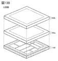
- FIG. 13A and 13B show perspective views of the semiconductor device 1150B.
- the semiconductor device 1150B has a semiconductor device 400a and a semiconductor device 400b on the arithmetic processing unit 1100.
- the arithmetic processing unit 1100, the semiconductor device 400a, and the semiconductor device 400b have regions that overlap each other.
- FIG. 13B shows the arithmetic processing unit 1100, the semiconductor device 400a, and the semiconductor device 400b separately.
- the semiconductor device 400a and the semiconductor device 400b function as a storage device.
- a NOR type storage device may be used for one of the semiconductor device 400a or the semiconductor device 400b, and a NAND type storage device may be used for the other.
- Both the semiconductor device 400a and the semiconductor device 400b may be a NAND type storage device or a NOR type storage device.
- the NOR type storage device includes DRAM, SRAM, and the like. Since the NOR type storage device can operate at a higher speed than the NAND type storage device, for example, a part of the semiconductor device 400a can be used as the main memory and / or the cache 1199.
- the stacking order of the semiconductor device 400a and the semiconductor device 400b may be reversed.
- FIG. 14A and 14B are perspective views of the semiconductor device 1150C.
- the semiconductor device 1150C has a configuration in which the arithmetic processing unit 1100 is sandwiched between the semiconductor device 400a and the semiconductor device 400b.
- the arithmetic processing unit 1100, the semiconductor device 400a, and the semiconductor device 400b have regions that overlap each other.
- FIG. 14B shows the arithmetic processing unit 1100, the semiconductor device 400a, and the semiconductor device 400b separately.
- both the communication speed between the semiconductor device 400a and the arithmetic processing device 1100 and the communication speed between the semiconductor device 400b and the arithmetic processing device 1100 can be increased. Moreover, the power consumption can be reduced as compared with the semiconductor device 1150B.
- the semiconductor device according to one aspect of the present invention can be used for an artificial neural network.
- An example of the configuration of the artificial neural network will be described below.
- FIG. 15A shows a configuration example of the neural network NN.
- the neural network NN can be composed of an input layer IL, an output layer OL, and an intermediate layer (hidden layer) HL.
- the input layer IL, the output layer OL, and the intermediate layer HL each have one or more neurons (units).
- the intermediate layer HL may be one layer or two or more layers.
- a neural network having two or more intermediate layers HL can also be called a DNN (deep neural network), and learning using a deep neural network can also be called deep learning.
- Input data is input to each neuron in the input layer IL, the output signal of the anterior layer or posterior layer neuron is input to each neuron in the intermediate layer HL, and the output of the anterior layer neuron is input to each neuron in the output layer OL.
- the signal is input.
- Each neuron may be connected to all neurons in the anterior and posterior layers (fully connected), or may be connected to some neurons.
- FIG. 15B shows an example of operation by neurons.
- two neurons in the presheaf layer that output a signal to the neuron N are shown.
- the output x 1 of the presheaf neuron and the output x 2 of the presheaf neuron are input to the neuron N.
- the sum of the multiplication result of the output x 1 and the weight w 1 (x 1 w 1 ) and the multiplication result of the output x 2 and the weight w 2 (x 2 w 2 ) is x 1 w 1 + x 2 w 2.
- the operation by the neuron includes the operation of adding the product of the output of the neuron in the previous layer and the weight, that is, the product-sum operation (x 1 w 1 + x 2 w 2 above ).
- This product-sum operation may be performed by software using a program or by hardware.
- a product-sum calculation circuit can be used.
- the product-sum calculation circuit a digital circuit or an analog circuit may be used.
- the processing speed can be improved and the power consumption can be reduced by reducing the circuit scale of the product-sum calculation circuit or reducing the number of times the memory is accessed.
- analog data is used as weight information.
- the semiconductor device 100 can hold analog data without converting it into a digital value. Therefore, conversion circuits such as DAC (Digital to Analog Converter) and / or ADC (Analog to Digital Converter) can be reduced, and power consumption and occupied area can be reduced.
- DAC Digital to Analog Converter
- ADC Analog to Digital Converter
- FIG. 16 A part of the cross-sectional structure of the semiconductor device is shown in FIG.
- the semiconductor device shown in FIG. 16 includes a transistor 550, a transistor 500, and a capacitive element 600.
- FIG. 17A is a top view of the transistor 500.
- FIG. 17B is a cross-sectional view of the portion L1-L2 shown by the alternate long and short dash line in FIG. 17A, and is a cross-sectional view of the transistor 500 in the channel length direction.
- FIG. 17C is a cross-sectional view of the portion W1-W2 shown by the alternate long and short dash line in FIG. 17A, and is a cross-sectional view of the transistor 500 in the channel width direction.
- the transistor 500 corresponds to an OS transistor included in the semiconductor device 100 shown in the above embodiment, that is, a transistor having an oxide semiconductor in a channel forming region.
- the transistor 550 corresponds to a Si transistor included in the drive circuit 410 shown in the above embodiment, that is, a transistor having silicon in the channel forming region.
- the transistor 500 is an OS transistor.
- the OS transistor has an extremely small off current. Therefore, it is possible to hold the data voltage or electric charge written to the storage node via the transistor 500 for a long period of time. That is, since the refresh operation frequency of the storage node is reduced or the refresh operation is not required, the power consumption of the semiconductor device can be reduced.
- the transistor 500 is provided above the transistor 550, and the capacitive element 600 is provided above the transistor 550 and the transistor 500.
- the transistor 550 is provided on the substrate 371.
- the substrate 371 is, for example, a p-type silicon substrate.
- the substrate 371 may be an n-type silicon substrate.
- the oxide layer 374 is preferably an insulating layer (also referred to as a BOX layer) formed by an embedded oxide (Burried oxide) in the substrate 371, for example, silicon oxide.
- the transistor 550 is provided on a single crystal silicon, so-called SOI (Silicon On Insulator) substrate, which is provided on the substrate 371 via an oxide layer 374.
- SOI Silicon On Insulator
- the substrate 371 of the SOI substrate is provided with an insulator 373 that functions as an element separation layer.
- the substrate 371 also has a well region 372.
- the well region 372 is a region to which n-type or p-type conductivity is imparted depending on the conductivity type of the transistor 550.
- the single crystal silicon in the SOI substrate is provided with a semiconductor region 375, a low resistance region 376a that functions as a source region or a drain region, and a low resistance region 376b. Further, a low resistance region 376c is provided on the well region 372.
- the transistor 550 can be provided so as to be superposed on the well region 372 to which the impurity element that imparts conductivity is added.
- the well region 372 can function as a bottom gate electrode of the transistor 550 by independently changing the potential via the low resistance region 376c. Therefore, the threshold voltage of the transistor 550 can be controlled.
- the threshold voltage of the transistor 550 can be made larger and the off-current can be reduced. Therefore, by applying a negative potential to the well region 372, the drain current when the potential applied to the gate electrode of the Si transistor is 0 V can be reduced. As a result, the power consumption based on the through current or the like in the arithmetic circuit having the transistor 550 can be reduced, and the arithmetic efficiency can be improved.
- the transistor 550 is preferably of the so-called Fin type, in which the upper surface of the semiconductor layer and the side surface in the channel width direction are covered with the conductor 378 via the insulator 377.
- the on-characteristics of the transistor 550 can be improved by increasing the effective channel width. Further, since the contribution of the electric field of the gate electrode can be increased, the off characteristic of the transistor 550 can be improved.
- the transistor 550 may be either a p-channel type transistor or an n-channel type transistor.
- the conductor 378 may function as a first gate (also referred to as a top gate) electrode. Further, the well region 372 may function as a second gate (also referred to as a bottom gate) electrode. In that case, the potential applied to the well region 372 can be controlled via the low resistance region 376c.
- the low resistance region 376a which is the region where the channel of the semiconductor region 375 is formed, the region in the vicinity thereof, the source region, or the drain region, and the low resistance region 376b, which is connected to the electrode controlling the potential of the well region 372.
- the region 376c or the like preferably contains a semiconductor such as a silicon-based semiconductor, and preferably contains single crystal silicon. Alternatively, it may be formed of a material having Ge (germanium), SiGe (silicon germanium), GaAs (gallium arsenide), GaAlAs (gallium aluminum arsenide), or the like. A configuration using silicon in which the effective mass is controlled by applying stress to the crystal lattice and changing the lattice spacing may be used. Alternatively, the transistor 550 may be a HEMT by using GaAs, GaAlAs, or the like.
- the well region 372, the low resistance region 376a, the low resistance region 376b, and the low resistance region 376c are elements that impart n-type conductivity such as arsenic and phosphorus, or boron, in addition to the semiconductor material applied to the semiconductor region 375. It contains an element that imparts p-type conductivity such as.
- the conductor 378 that functions as a gate electrode is a semiconductor material such as silicon, a metal material, or an alloy that contains an element that imparts n-type conductivity such as arsenic or phosphorus, or an element that imparts p-type conductivity such as boron.
- a material or a conductive material such as a metal oxide material can be used.
- a silicide such as nickel silicide may be used as the conductor 378.
- the threshold voltage of the transistor can be adjusted by selecting the material of the conductor. Specifically, it is preferable to use a material such as titanium nitride or tantalum nitride for the conductor. Further, in order to achieve both conductivity and embedding property, it is preferable to use a metal material such as tungsten or aluminum as a laminate for the conductor, and it is particularly preferable to use tungsten in terms of heat resistance.
- the low resistance region 376a, the low resistance region 376b, and the low resistance region 376c may be configured to be provided by laminating another conductor, for example, a silicide such as nickel silicide. With this configuration, the conductivity of the region that functions as an electrode can be enhanced. At this time, an insulator that functions as a side wall spacer (also referred to as a side wall insulating layer) may be provided on the side surface of the conductor 378 that functions as the gate electrode and the side surface of the insulator that functions as the gate insulating film. .. With this configuration, it is possible to prevent the conductor 378 and the low resistance region 376a and the low resistance region 376b from being in a conductive state.
- a silicide such as nickel silicide
- An insulator 379, an insulator 381, an insulator 383, and an insulator 385 are laminated in this order so as to cover the transistor 550.
- the insulator 379, the insulator 381, the insulator 383, and the insulator 385 for example, silicon oxide, silicon oxide, silicon nitride, silicon nitride, aluminum oxide, aluminum oxide, aluminum nitride, aluminum nitride, etc. are used. Just do it.
- silicon oxide refers to a material having a higher oxygen content than nitrogen as its composition
- silicon nitride as its composition means a material having a higher nitrogen content than oxygen as its composition. Is shown.
- aluminum nitride refers to a material whose composition has a higher oxygen content than nitrogen
- aluminum nitride refers to a material whose composition has a higher nitrogen content than oxygen. Is shown.
- the insulator 381 may have a function as a flattening film for flattening a step generated by a transistor 550 or the like provided below the insulator 381.
- the upper surface of the insulator 381 may be flattened by a flattening treatment using a chemical mechanical polishing (CMP) method or the like in order to improve the flatness.
- CMP chemical mechanical polishing
- the insulator 383 it is preferable to use a film having a barrier property so that hydrogen and impurities do not diffuse in the region where the transistor 500 is provided from the substrate 371 or the transistor 550.
- a film having a barrier property against hydrogen for example, silicon nitride formed by the CVD method can be used.
- hydrogen may diffuse into a semiconductor element having an oxide semiconductor such as a transistor 500, so that the characteristics of the semiconductor element may deteriorate. Therefore, it is preferable to use a film that suppresses the diffusion of hydrogen between the transistor 500 and the transistor 550.
- the membrane that suppresses the diffusion of hydrogen is a membrane that desorbs a small amount of hydrogen.
- the amount of hydrogen desorbed can be analyzed using, for example, a heated desorption gas analysis method (TDS).
- TDS heated desorption gas analysis method
- the amount of hydrogen desorbed from the insulator 383 is such that the amount desorbed in terms of hydrogen atoms is converted per area of the insulator 383 when the surface temperature of the film is in the range of 50 ° C. to 500 ° C. It may be 10 ⁇ 10 15 atoms / cm 2 or less, preferably 5 ⁇ 10 15 atoms / cm 2 or less.
- the insulator 385 preferably has a lower dielectric constant than the insulator 383.
- the relative permittivity of the insulator 385 is preferably less than 4, more preferably less than 3.
- the relative permittivity of the insulator 385 is preferably 0.7 times or less, more preferably 0.6 times or less, the relative permittivity of the insulator 383.
- the insulator 379, the insulator 381, the insulator 383, and the insulator 385 are embedded with a capacitance element 600, a conductor 328 connected to the transistor 500, a conductor 330, and the like.
- the conductor 328 and the conductor 330 have a function as a plug or a wiring.
- the conductor having a function as a plug or a wiring may collectively give a plurality of configurations and give the same reference numeral.
- the wiring and the plug connected to the wiring may be integrated. That is, a part of the conductor may function as a wiring, and a part of the conductor may function as a plug.
- each plug and wiring As the material of each plug and wiring (conductor 328, conductor 330, etc.), a conductive material such as a metal material, an alloy material, a metal nitride material, or a metal oxide material is used as a single layer or laminated. be able to. It is preferable to use a refractory material such as tungsten or molybdenum that has both heat resistance and conductivity, and it is preferable to use tungsten. Alternatively, it is preferably formed of a low resistance conductive material such as aluminum or copper. Wiring resistance can be reduced by using a low resistance conductive material.
- a wiring layer may be provided on the insulator 385 and the conductor 330.
- the insulator 350, the insulator 352, and the insulator 354 are laminated in this order.
- a conductor 356 is formed on the insulator 350, the insulator 352, and the insulator 354.
- the conductor 356 has a function as a plug or wiring for connecting to the transistor 550.
- the conductor 356 can be provided by using the same materials as the conductor 328 and the conductor 330.
- the insulator 350 it is preferable to use an insulator having a barrier property against hydrogen, similarly to the insulator 383.
- the conductor 356 preferably contains a conductor having a barrier property against hydrogen.
- a conductor having a barrier property against hydrogen is formed in the opening of the insulator 350 having a barrier property against hydrogen.
- the conductor having a barrier property against hydrogen for example, tantalum nitride or the like may be used. Further, by laminating tantalum nitride and tungsten having high conductivity, it is possible to suppress the diffusion of hydrogen from the transistor 550 while maintaining the conductivity as wiring. In this case, it is preferable that the tantalum nitride layer having a barrier property against hydrogen is in contact with the insulator 350 having a barrier property against hydrogen.
- a wiring layer may be provided on the insulator 354 and the conductor 356.
- the insulator 360, the insulator 362, and the insulator 364 are laminated in this order.
- a conductor 366 is formed in the insulator 360, the insulator 362, and the insulator 364.
- the conductor 366 has a function as a plug or wiring.
- the conductor 366 can be provided by using the same materials as the conductor 328 and the conductor 330.
- the insulator 360 it is preferable to use an insulator having a barrier property against hydrogen, similarly to the insulator 383.
- the conductor 366 preferably contains a conductor having a barrier property against hydrogen.
- a conductor having a barrier property against hydrogen is formed in the opening of the insulator 360 having a barrier property against hydrogen.
- a wiring layer may be provided on the insulator 364 and the conductor 366.
- the insulator 370, the insulator 369, and the insulator 368 are laminated in this order.
- a conductor 376 is formed on the insulator 370, the insulator 369, and the insulator 368.
- the conductor 376 has a function as a plug or wiring.
- the conductor 376 can be provided by using the same materials as the conductor 328 and the conductor 330.
- the insulator 370 it is preferable to use an insulator having a barrier property against hydrogen, similarly to the insulator 383.
- the conductor 376 preferably contains a conductor having a barrier property against hydrogen.
- a conductor having a barrier property against hydrogen is formed in the opening of the insulator 370 having a barrier property against hydrogen.
- a wiring layer may be provided on the insulator 368 and the conductor 376.
- the insulator 380, the insulator 382, and the insulator 384 are laminated in this order.
- a conductor 386 is formed on the insulator 380, the insulator 382, and the insulator 384.
- the conductor 386 has a function as a plug or wiring.
- the conductor 386 can be provided by using the same materials as the conductor 328 and the conductor 330.
- the insulator 380 it is preferable to use an insulator having a barrier property against hydrogen, similarly to the insulator 383.
- the conductor 386 preferably contains a conductor having a barrier property against hydrogen.
- a conductor having a barrier property against hydrogen is formed in the opening of the insulator 380 having a barrier property against hydrogen.
- the semiconductor device according to the present embodiment has been described. It is not limited to this.
- the number of wiring layers similar to the wiring layer containing the conductor 356 may be three or less, or the number of wiring layers similar to the wiring layer containing the conductor 356 may be five or more.
- An insulator 510, an insulator 512, an insulator 514, and an insulator 516 are laminated in this order on the insulator 384.
- any of the insulator 510, the insulator 512, the insulator 514, and the insulator 516 it is preferable to use a substance having a barrier property against oxygen and hydrogen.
- the insulator 510 and the insulator 514 it is preferable to use a film having a barrier property against hydrogen and impurities in the region where the transistor 500 is provided, for example, from the region where the substrate 371 or the transistor 550 is provided. Therefore, the same material as the insulator 383 can be used.
- silicon nitride formed by the CVD method can be used as an example of a film having a barrier property against hydrogen.
- hydrogen may diffuse into a semiconductor element having an oxide semiconductor such as a transistor 500, so that the characteristics of the semiconductor element may deteriorate. Therefore, it is preferable to use a film that suppresses the diffusion of hydrogen between the transistor 500 and the transistor 550.
- the film having a barrier property against hydrogen for example, it is preferable to use metal oxides such as aluminum oxide, hafnium oxide, and tantalum oxide for the insulator 510 and the insulator 514.
- metal oxides such as aluminum oxide, hafnium oxide, and tantalum oxide for the insulator 510 and the insulator 514.
- aluminum oxide has a high blocking effect that does not allow the membrane to permeate both oxygen and impurities such as hydrogen and water that cause fluctuations in the electrical characteristics of the transistor. Therefore, aluminum oxide can prevent impurities such as hydrogen and moisture from being mixed into the transistor 500 during and after the manufacturing process of the transistor. In addition, it is possible to suppress the release of oxygen from the oxides constituting the transistor 500. Therefore, it is suitable for use as a protective film for the transistor 500.
- the same material as the insulator 379 can be used for the insulator 512 and the insulator 516. Further, by applying a material having a relatively low dielectric constant to these insulators, it is possible to reduce the parasitic capacitance generated between the wirings.
- a silicon oxide film, a silicon nitride film, or the like can be used as the insulator 512 and the insulator 516.
- the insulator 510, the insulator 512, the insulator 514, and the insulator 516 are embedded with a conductor 518, a conductor (for example, a conductor 503) constituting the transistor 500, and the like.
- the conductor 518 has a function as a plug or wiring for connecting to the capacitance element 600 or the transistor 550.
- the conductor 518 can be provided by using the same material as the conductor 328 and the conductor 330.
- the conductor 510 and the conductor 518 in the region in contact with the insulator 514 are preferably conductors having a barrier property against oxygen, hydrogen, and water.
- the transistor 550 and the transistor 500 can be separated by a layer having a barrier property against oxygen, hydrogen, and water, and the diffusion of hydrogen from the transistor 550 to the transistor 500 can be suppressed.
- a transistor 500 is provided above the insulator 516.
- the transistor 500 has a conductor 503 arranged so as to be embedded in the insulator 514 and the insulator 516, and an insulator 520 arranged on the insulator 516 and the insulator 503.
- the insulator 524 placed on the insulator 522, the oxide 530a placed on the insulator 524, and the oxide 530a.
- the arranged oxide 530b, the conductors 542a and 542b arranged apart from each other on the oxide 530b, and the conductors 542a and 542b are arranged between the conductors 542a and 542b.
- It has an insulator 580 on which an opening is formed by superimposing, an insulator 545 arranged on the bottom surface and side surfaces of the opening, and a conductor 560 arranged on the forming surface of the insulator 545.
- the insulator 544 is arranged between the oxide 530a, the oxide 530b, the conductor 542a, and the conductor 542b and the insulator 580.
- the conductor 560 includes a conductor 560a provided inside the insulator 545 and a conductor 560b provided so as to be embedded inside the conductor 560a. It is preferable to have.
- the insulator 574 is arranged on the insulator 580, the conductor 560, and the insulator 545.
- oxide 530a and oxide 530b may be collectively referred to as oxide 530.
- the transistor 500 shows a configuration in which two layers of oxide 530a and oxide 530b are laminated in a region where a channel is formed and in the vicinity thereof, but the present invention is not limited to this.
- a single layer of the oxide 530b or a laminated structure of three or more layers may be provided.
- the conductor 560 is shown as a two-layer laminated structure, but the present invention is not limited to this.
- the conductor 560 may have a single-layer structure or a laminated structure of three or more layers.
- the transistor 500 shown in FIGS. 16, 17A, and 17C is an example, and the transistor 500 is not limited to the configuration, and an appropriate transistor may be used depending on the circuit configuration and / or the driving method.
- the conductor 560 functions as a gate electrode of the transistor 500, and the conductor 542a and the conductor 542b function as a source electrode or a drain electrode, respectively.
- the conductor 560 is formed so as to be embedded in the opening of the insulator 580 and the region sandwiched between the conductor 542a and the conductor 542b.
- the arrangement of the conductor 560, the conductor 542a and the conductor 542b is self-aligned with respect to the opening of the insulator 580. That is, in the transistor 500, the gate electrode can be arranged in a self-aligned manner between the source electrode and the drain electrode. Therefore, since the conductor 560 can be formed without providing the alignment margin, the occupied area of the transistor 500 can be reduced. As a result, the semiconductor device can be miniaturized and highly integrated.
- the conductor 560 is formed in a region between the conductor 542a and the conductor 542b in a self-aligned manner, the conductor 560 does not have a region that overlaps with the conductor 542a or the conductor 542b. Thereby, the parasitic capacitance formed between the conductor 560 and the conductors 542a and 542b can be reduced. Therefore, the switching speed of the transistor 500 can be improved and a high frequency characteristic can be provided.
- the conductor 560 may function as a first gate (also referred to as a gate or top gate) electrode. Further, the conductor 503 may function as a second gate (also referred to as a back gate or a bottom gate) electrode.
- the threshold voltage of the transistor 500 can be controlled by changing the potential applied to the conductor 503 independently of the potential applied to the conductor 560 without interlocking with the potential applied to the conductor 560. In particular, by applying a negative potential to the conductor 503, the threshold voltage of the transistor 500 can be made larger and the off-current can be reduced. Therefore, when a negative potential is applied to the conductor 503, the drain current when the potential applied to the conductor 560 is 0 V can be made smaller than when it is not applied.
- the conductor 503 is arranged so as to overlap the oxide 530 and the conductor 560. As a result, when a potential is applied to the conductor 560 and the conductor 503, the electric field generated from the conductor 560 and the electric field generated from the conductor 503 are connected to cover the channel forming region formed in the oxide 530. Can be done.
- the configuration of the transistor that electrically surrounds the channel formation region by the electric field of the pair of gate electrodes is referred to as a curved channel (S-channel) configuration.
- S-channel configuration disclosed in the present specification and the like is different from the Fin type configuration and the planar type configuration.
- the conductor 503 has the same structure as the conductor 518, and the conductor 503a is formed in contact with the inner wall of the opening of the insulator 514 and the insulator 516, and the conductor 503b is further formed inside.
- the transistor 500 shows a configuration in which the conductor 503a and the conductor 503b are laminated, the present invention is not limited to this.
- the conductor 503 may be provided as a single layer or a laminated structure having three or more layers.
- the conductor 503a it is preferable to use a conductive material having a function of suppressing the diffusion of impurities such as hydrogen atoms, hydrogen molecules, water molecules, and copper atoms (the above impurities are difficult to permeate).
- a conductive material having a function of suppressing the diffusion of oxygen for example, at least one oxygen atom, oxygen molecule, etc.
- the function of suppressing the diffusion of impurities or oxygen is a function of suppressing the diffusion of any one or all of the above impurities or the above oxygen.
- the conductor 503a since the conductor 503a has a function of suppressing the diffusion of oxygen, it is possible to prevent the conductor 503b from being oxidized and the conductivity from being lowered.
- the conductor 503 When the conductor 503 also functions as a wiring, it is preferable to use a highly conductive conductive material containing tungsten, copper, or aluminum as a main component for the conductor 503b.
- the conductor 503 is shown by laminating the conductor 503a and the conductor 503b, but the conductor 503 may have a single-layer structure.
- the insulator 520, the insulator 522, and the insulator 524 have a function as a second gate insulating film.
- the insulator 524 in contact with the oxide 530 it is preferable to use an insulator containing more oxygen than oxygen satisfying the stoichiometric composition.
- the oxygen is easily released from the membrane by heating.
- oxygen released by heating may be referred to as "excess oxygen”. That is, it is preferable that the insulator 524 is formed with a region containing excess oxygen (also referred to as “excess oxygen region”).
- the defective Functions as a donor, sometimes electrons serving as carriers are generated.
- a part of hydrogen may be combined with oxygen that is bonded to a metal atom to generate an electron as a carrier. Therefore, a transistor using an oxide semiconductor containing a large amount of hydrogen tends to have a normally-on characteristic. Further, since hydrogen in the oxide semiconductor easily moves due to stress such as heat and electric field, if the oxide semiconductor contains a large amount of hydrogen, the reliability of the transistor may deteriorate.
- the V O H to obtain a sufficiently reduced oxide semiconductor (referred to as “dewatering” or “dehydrogenation process” also.) Water in the oxide semiconductor, to remove impurities such as hydrogen It is important to supply oxygen to the oxide semiconductor to compensate for the oxygen deficiency (also referred to as “dehydrogenation treatment”).
- the V O H oxide semiconductor impurity is sufficiently reduced such by using a channel formation region of the transistor, it is possible to have stable electrical characteristics.
- an oxide material in which a part of oxygen is desorbed by heating is an oxide having a desorption amount of oxygen converted into oxygen atoms of 1.0 ⁇ 10 18 atoms / cm 3 or more, preferably 1 in TDS (Thermal Desorption Spectroscopy) analysis.
- the surface temperature of the film during the TDS analysis is preferably in the range of 100 ° C. or higher and 700 ° C. or lower, or 100 ° C. or higher and 400 ° C. or lower.
- the insulator having the excess oxygen region and the oxide 530 may be brought into contact with each other to perform one or more of heat treatment, microwave treatment, or RF treatment.
- heat treatment microwave treatment, or RF treatment.
- water or hydrogen in the oxide 530 can be removed.
- reactions occur which bonds VoH is disconnected, when other words happening reaction of "V O H ⁇ Vo + H", it can be dehydrogenated.
- the hydrogen generated as oxygen combines with H 2 O, it may be removed from the oxide 530 or oxide 530 near the insulator.
- a part of hydrogen may be gettered to the conductor 542a and the conductor 542b.
- the microwave processing for example, it is preferable to use an apparatus having a power source for generating high-density plasma or an apparatus having a power source for applying RF to the substrate side.
- an apparatus having a power source for generating high-density plasma for example, by using a gas containing oxygen and using a high-density plasma, high-density oxygen radicals can be generated, and by applying RF to the substrate side, the oxygen radicals generated by the high-density plasma can be generated.
- the pressure may be 133 Pa or more, preferably 200 Pa or more, and more preferably 400 Pa or more.
- oxygen and argon are used as the gas to be introduced into the apparatus for performing microwave treatment, and the oxygen flow rate ratio (O 2 / (O 2 + Ar)) is 50% or less, preferably 10% or more and 30. It is better to do it at% or less.
- the heat treatment may be performed, for example, at 100 ° C. or higher and 450 ° C. or lower, more preferably 350 ° C. or higher and 400 ° C. or lower.
- the heat treatment is performed in an atmosphere of nitrogen gas or an inert gas, or an atmosphere containing 10 ppm or more, 1% or more, or 10% or more of an oxidizing gas.
- the heat treatment is preferably performed in an oxygen atmosphere.
- oxygen can be supplied to the oxide 530 to reduce oxygen deficiency (VO ).
- the heat treatment may be performed in a reduced pressure state.
- the heat treatment may be carried out in an atmosphere containing 10 ppm or more, 1% or more, or 10% or more of an oxidizing gas in order to supplement the desorbed oxygen after the heat treatment in an atmosphere of nitrogen gas or an inert gas. good.
- the heat treatment may be performed in an atmosphere containing 10 ppm or more, 1% or more, or 10% or more of the oxidizing gas, and then the heat treatment may be continuously performed in an atmosphere of nitrogen gas or an inert gas.
- the oxygen deficiency in the oxide 530 can be repaired by the supplied oxygen, in other words, the reaction "Vo + O ⁇ null" can be promoted. Further, since the oxygen supplied to the hydrogen remaining in the oxide 530 is reacted to remove the hydrogen as H 2 O (to dehydration) can. Thus, the hydrogen remained in the oxide 530 can be prevented from recombine V O H is formed by oxygen vacancies.
- the insulator 524 has an excess oxygen region, it is preferable that the insulator 522 has a function of suppressing the diffusion of oxygen (for example, oxygen atom, oxygen molecule, etc.) (the oxygen is difficult to permeate).
- oxygen for example, oxygen atom, oxygen molecule, etc.
- the insulator 522 has a function of suppressing the diffusion of oxygen and impurities, the oxygen contained in the oxide 530 does not diffuse to the insulator 520 side, which is preferable. Further, it is possible to suppress the conductor 503 from reacting with the oxygen contained in the insulator 524 and / or the oxide 530.
- the insulator 522 may be, for example, aluminum oxide, hafnium oxide, an oxide containing aluminum and hafnium (hafnium aluminate), tantalum oxide, zirconate oxide, lead zirconate titanate (PZT), strontium titanate (SrTIO 3 ), or It is preferable to use an insulator containing a so-called high-k material such as (Ba, Sr) TiO 3 (BST) in a single layer or in a laminated state. As transistors become finer and more integrated, problems such as leakage current may occur due to the thinning of the gate insulating film. By using a high-k material for the insulator that functions as a gate insulating film, it is possible to reduce the gate potential during transistor operation while maintaining the physical film thickness.
- a so-called high-k material such as (Ba, Sr) TiO 3 (BST)
- an insulator containing an oxide of one or both of aluminum and hafnium which are insulating materials having a function of suppressing diffusion of impurities and oxygen (the above-mentioned oxygen is difficult to permeate).
- the insulator containing one or both oxides of aluminum and hafnium it is preferable to use aluminum oxide, hafnium oxide, an oxide containing aluminum and hafnium (hafnium aluminate) and the like.
- the insulator 522 is a layer that suppresses the release of oxygen from the oxide 530 and the mixing of impurities such as hydrogen from the peripheral portion of the transistor 500 into the oxide 530. Functions as.
- aluminum oxide, bismuth oxide, germanium oxide, niobium oxide, silicon oxide, titanium oxide, tungsten oxide, yttrium oxide, and zirconium oxide may be added to these insulators.
- these insulators may be nitrided. Silicon oxide, silicon oxide nitride, or silicon nitride may be laminated on the above insulator.
- the insulator 520 is preferably thermally stable.
- silicon oxide and silicon oxynitride are suitable because they are thermally stable.
- by combining the insulator of the high-k material with silicon oxide or silicon oxide nitride it is possible to obtain an insulator 520 having a laminated structure that is thermally stable and has a high relative permittivity.
- an insulator 520, an insulator 522, and an insulator 524 are shown as a second gate insulating film having a three-layer laminated structure, but the second gate.
- the insulating film may have a single layer, two layers, or a laminated structure of four or more layers.
- the laminated structure is not limited to the same material, and may be a laminated structure made of different materials.
- the transistor 500 uses a metal oxide that functions as an oxide semiconductor for the oxide 530 containing the channel forming region.
- oxide 530 In-M-Zn oxide (element M is aluminum, gallium, yttrium, tin, copper, vanadium, beryllium, boron, titanium, iron, nickel, germanium, zirconium, molybdenum, lanthanum, cerium).
- Neodim, Hafnium, Tantal, Tungsten, Magnesium, etc. (one or more) and the like may be used.
- the metal oxide that functions as an oxide semiconductor may be formed by a sputtering method or an ALD (Atomic Layer Deposition) method.
- ALD Atomic Layer Deposition
- the metal oxide that functions as a channel forming region in the oxide 530 it is preferable to use a metal oxide having a band gap of preferably 2 eV or more, more preferably 2.5 eV or more. In this way, by using a metal oxide having a large bandgap, the off-current of the transistor can be reduced.
- the oxide 530 can suppress the diffusion of impurities into the oxide 530b from the composition formed below the oxide 530a.
- the oxide 530 preferably has a laminated structure of a plurality of oxide layers having different atomic number ratios of each metal atom.
- the atomic number ratio of the element M in the constituent elements is larger than the atomic number ratio of the element M in the constituent elements in the metal oxide used in the oxide 530b. Is preferable.
- the atomic number ratio of the element M to In is preferably larger than the atomic number ratio of the element M to In in the metal oxide used for the oxide 530b.
- the atomic number ratio of In to the element M is preferably larger than the atomic number ratio of In to the element M in the metal oxide used for the oxide 530a.
- the energy at the lower end of the conduction band of the oxide 530a is higher than the energy at the lower end of the conduction band of the oxide 530b.
- the electron affinity of the oxide 530a is smaller than the electron affinity of the oxide 530b.
- the energy level at the lower end of the conduction band changes gently.
- the energy level at the lower end of the conduction band at the junction of the oxide 530a and the oxide 530b is continuously changed or continuously bonded. In order to do so, it is preferable to reduce the defect level density of the mixed layer formed at the interface between the oxide 530a and the oxide 530b.
- the oxide 530a and the oxide 530b have a common element (main component) other than oxygen, a mixed layer having a low defect level density can be formed.
- the oxide 530b is an In-Ga-Zn oxide
- the main path of the carrier is the oxide 530b.
- the defect level density at the interface between the oxide 530a and the oxide 530b can be lowered. Therefore, the influence of interfacial scattering on carrier conduction is reduced, and the transistor 500 can obtain a high on-current.
- a conductor 542a and a conductor 542b that function as a source electrode and a drain electrode are provided on the oxide 530b.
- the conductors 542a and 542b include aluminum, chromium, copper, silver, gold, platinum, tantalum, nickel, titanium, molybdenum, tungsten, hafnium, vanadium, niobium, manganese, magnesium, zirconium, beryllium, indium, and ruthenium.
- Iridium, strontium, lanthanum, or an alloy containing the above-mentioned metal element as a component, or an alloy in which the above-mentioned metal element is combined is preferably used.
- tantalum nitride, titanium nitride, tungsten, nitrides containing titanium and aluminum, nitrides containing tantalum and aluminum, ruthenium oxide, ruthenium nitride, oxides containing strontium and ruthenium, oxides containing lanthanum and nickel, etc. are used. Is preferable.
- tantalum nitride, titanium nitride, nitrides containing titanium and aluminum, nitrides containing tantalum and aluminum, ruthenium oxide, ruthenium nitride, oxides containing strontium and ruthenium, and oxides containing lanthanum and nickel are difficult to oxidize.
- a metal nitride film such as tantalum nitride is preferable because it has a barrier property against hydrogen or oxygen.
- the conductor 542a and the conductor 542b are shown as a single-layer structure, but a laminated structure of two or more layers may be used.
- a tantalum nitride film and a tungsten film may be laminated.
- the titanium film and the aluminum film may be laminated.
- a two-layer structure in which an aluminum film is laminated on a tungsten film a two-layer structure in which a copper film is laminated on a copper-magnesium-aluminum alloy film, a two-layer structure in which a copper film is laminated on a titanium film, and a two-layer structure in which a copper film is laminated on a titanium film. It may have a two-layer structure in which copper films are laminated.
- a transparent conductive material containing indium oxide, tin oxide or zinc oxide may be used.
- a region 543a and a region 543b may be formed as low resistance regions at the interface of the oxide 530 with the conductor 542a (conductor 542b) and its vicinity.
- the region 543a functions as one of the source region or the drain region
- the region 543b functions as the other of the source region or the drain region.
- a channel forming region is formed in a region sandwiched between the region 543a and the region 543b.
- the oxygen concentration in the region 543a (region 543b) may be reduced. Further, in the region 543a (region 543b), a metal compound layer containing the metal contained in the conductor 542a (conductor 542b) and the component of the oxide 530 may be formed. In such a case, the carrier density of the region 543a (region 543b) increases, and the region 543a (region 543b) becomes a low resistance region.
- the insulator 544 is provided so as to cover the conductor 542a and the conductor 542b, and suppresses the oxidation of the conductor 542a and the conductor 542b. At this time, the insulator 544 may be provided so as to cover the side surface of the oxide 530 and come into contact with the insulator 524.
- insulator 544 a metal oxide containing one or more selected from hafnium, aluminum, gallium, yttrium, zirconium, tungsten, titanium, tantalum, nickel, germanium, neodymium, lanthanum, magnesium, etc. Can be used. Further, as the insulator 544, silicon nitride oxide, silicon nitride or the like can also be used.
- the insulator 544 it is preferable to use aluminum or an oxide containing one or both oxides of hafnium, such as aluminum oxide, hafnium oxide, aluminum, and an oxide containing hafnium (hafnium aluminate). ..
- hafnium aluminate has higher heat resistance than the hafnium oxide film. Therefore, it is preferable because it is difficult to crystallize in the heat treatment in the subsequent step.
- the conductors 542a and 542b are materials having oxidation resistance or materials whose conductivity does not significantly decrease even if oxygen is absorbed, the insulator 544 is not an essential configuration. It may be appropriately designed according to the desired transistor characteristics.
- the insulator 544 By having the insulator 544, it is possible to prevent impurities such as water and hydrogen contained in the insulator 580 from diffusing into the oxide 530b. In addition, oxidation of the conductor 542 due to excess oxygen contained in the insulator 580 can be suppressed.
- the insulator 545 functions as a first gate insulating film.
- the insulator 545 is preferably formed by using an insulator that contains excess oxygen and releases oxygen by heating, similarly to the above-mentioned insulator 524.
- silicon oxide with excess oxygen silicon oxide, silicon nitride, silicon nitride, silicon oxide with fluorine added, silicon oxide with carbon added, carbon, and silicon oxide with nitrogen added, vacancies Silicon oxide having can be used.
- silicon oxide and silicon oxide nitride are preferable because they are stable against heat.
- the insulator containing excess oxygen as the insulator 545, oxygen can be effectively supplied from the insulator 545 to the channel forming region of the oxide 530b. Further, similarly to the insulator 524, it is preferable that the concentration of impurities such as water or hydrogen in the insulator 545 is reduced.
- the film thickness of the insulator 545 is preferably 1 nm or more and 20 nm or less. Further, the above-mentioned microwave treatment may be performed before and / or after the formation of the insulator 545.
- a metal oxide may be provided between the insulator 545 and the conductor 560.
- the metal oxide preferably suppresses oxygen diffusion from the insulator 545 to the conductor 560.
- the diffusion of excess oxygen from the insulator 545 to the conductor 560 is suppressed. That is, it is possible to suppress a decrease in the amount of excess oxygen supplied to the oxide 530.
- oxidation of the conductor 560 due to excess oxygen can be suppressed.
- a material that can be used for the insulator 544 may be used.
- the insulator 545 may have a laminated structure as in the case of the second gate insulating film.
- an insulator that functions as a gate insulating film is made of a high-k material and heat.
- the conductor 560 functioning as the first gate electrode is shown as a two-layer structure in FIGS. 17B and 17C, it may have a single-layer structure or a laminated structure of three or more layers.
- Conductor 560a is a hydrogen atom, a hydrogen molecule, a water molecule, a nitrogen atom, a nitrogen molecule, nitric oxide molecule (N 2 O, NO, etc. NO 2), conductive having a function of suppressing the diffusion of impurities such as copper atoms It is preferable to use a material. Alternatively, it is preferable to use a conductive material having a function of suppressing the diffusion of oxygen (for example, at least one oxygen atom, oxygen molecule, etc.). Since the conductor 560a has a function of suppressing the diffusion of oxygen, it is possible to prevent the conductor 560b from being oxidized by the oxygen contained in the insulator 545 to reduce the conductivity.
- the conductive material having a function of suppressing the diffusion of oxygen for example, tantalum, tantalum nitride, ruthenium, ruthenium oxide and the like are preferably used.
- an oxide semiconductor applicable to the oxide 530 can be used as the conductor 560a. In that case, by forming the conductor 560b into a film by a sputtering method, the electric resistance value of the conductor 560a can be lowered to form a conductor. This can be called an OC (Oxide Conductor) electrode.
- the conductor 560b it is preferable to use a conductive material containing tungsten, copper, or aluminum as a main component. Further, since the conductor 560b also functions as wiring, it is preferable to use a conductor having high conductivity. For example, a conductive material containing tungsten, copper, or aluminum as a main component can be used. Further, the conductor 560b may have a laminated structure, for example, a laminated structure of titanium or titanium nitride and the conductive material.
- the insulator 580 is provided on the conductor 542a and the conductor 542b via the insulator 544.
- the insulator 580 preferably has an excess oxygen region.
- silicon, resin, or the like silicon oxide and silicon oxide nitride are preferable because they are thermally stable.
- silicon oxide and silicon oxide having pores are preferable because an excess oxygen region can be easily formed in a later step.
- the insulator 580 preferably has an excess oxygen region. By providing the insulator 580 in which oxygen is released by heating, the oxygen in the insulator 580 can be efficiently supplied to the oxide 530. It is preferable that the concentration of impurities such as water and hydrogen in the insulator 580 is reduced.
- the opening of the insulator 580 is formed so as to overlap the region between the conductor 542a and the conductor 542b.
- the conductor 560 is formed so as to be embedded in the opening of the insulator 580 and the region sandwiched between the conductor 542a and the conductor 542b.
- the conductor 560 may have a shape having a high aspect ratio.
- the conductor 560 is provided so as to be embedded in the opening of the insulator 580, even if the conductor 560 has a shape having a high aspect ratio, the conductor 560 is formed without collapsing during the process. Can be done.
- the insulator 574 is preferably provided in contact with the upper surface of the insulator 580, the upper surface of the conductor 560, and the upper surface of the insulator 545.
- an excess oxygen region can be provided in the insulator 545 and the insulator 580. Thereby, oxygen can be supplied into the oxide 530 from the excess oxygen region.
- the insulator 574 use one or more metal oxides selected from hafnium, aluminum, gallium, yttrium, zirconium, tungsten, titanium, tantalum, nickel, germanium, magnesium and the like. Can be done.
- aluminum oxide has a high barrier property and can suppress the diffusion of hydrogen and nitrogen even in a thin film of 0.5 nm or more and 3.0 nm or less. Therefore, the aluminum oxide formed by the sputtering method can have a function as a barrier film for impurities such as hydrogen as well as an oxygen supply source.
- the insulator 581 that functions as an interlayer film on the insulator 574.
- the insulator 581 preferably has a reduced concentration of impurities such as water and hydrogen in the film.
- the conductor 540a and the conductor 540b are arranged in the openings formed in the insulator 581, the insulator 574, the insulator 580, and the insulator 544.
- the conductor 540a and the conductor 540b are provided so as to face each other with the conductor 560 interposed therebetween.
- the conductor 540a and the conductor 540b have the same configuration as the conductor 546 and the conductor 548 described later.
- An insulator 582 is provided on the insulator 581.
- the insulator 582 it is preferable to use a substance having a barrier property against oxygen and hydrogen. Therefore, the same material as the insulator 514 can be used for the insulator 582.
- a metal oxide such as aluminum oxide, hafnium oxide, and tantalum oxide for the insulator 582.
- aluminum oxide has a high blocking effect that does not allow the membrane to permeate both oxygen and impurities such as hydrogen and water that cause fluctuations in the electrical characteristics of the transistor. Therefore, aluminum oxide can prevent impurities such as hydrogen and moisture from being mixed into the transistor 500 during and after the manufacturing process of the transistor. In addition, it is possible to suppress the release of oxygen from the oxides constituting the transistor 500. Therefore, it is suitable for use as a protective film for the transistor 500.
- an insulator 586 is provided on the insulator 582.
- the same material as the insulator 379 can be used. Further, by applying a material having a relatively low dielectric constant to these insulators, it is possible to reduce the parasitic capacitance generated between the wirings.
- a silicon oxide film, a silicon nitride film, or the like can be used as the insulator 586.
- the insulator 520, the insulator 522, the insulator 524, the insulator 544, the insulator 580, the insulator 574, the insulator 581, the insulator 582, and the insulator 586 include the conductor 546 and the conductor 548. Is embedded.
- the conductor 546 and the conductor 548 have a function as a plug or wiring for connecting to the capacitive element 600, the transistor 500, or the transistor 550.
- the conductor 546 and the conductor 548 can be provided by using the same materials as the conductor 328 and the conductor 330.
- an opening may be formed so as to surround the transistor 500, and an insulator having a high barrier property against hydrogen or water may be formed so as to cover the opening.
- an insulator having a high barrier property against hydrogen or water By wrapping the transistor 500 with the above-mentioned insulator having a high barrier property, it is possible to prevent moisture and hydrogen from entering from the outside.
- a plurality of transistors 500 may be put together and wrapped with an insulator having a high barrier property against hydrogen or water.
- the insulator having a high barrier property to hydrogen or water for example, the same material as the insulator 522 or the insulator 514 may be used.
- the capacitive element 600 has a conductor 610, a conductor 620, and an insulator 630.
- the conductor 612 may be provided on the conductor 546 and the conductor 548.
- the conductor 612 has a function as a plug or wiring for connecting to the transistor 500.
- the conductor 610 has a function as an electrode of the capacitive element 600.
- the conductor 612 and the conductor 610 can be formed at the same time.
- the conductor 612 and the conductor 610 include a metal film containing an element selected from molybdenum, titanium, tantalum, tungsten, aluminum, copper, chromium, neodymium, and scandium, or a metal nitride film containing the above-mentioned elements as components.
- a metal nitride film, titanium nitride film, molybdenum nitride film, tungsten nitride film and the like can be used.
- indium tin oxide, indium oxide containing tungsten oxide, indium zinc oxide containing tungsten oxide, indium oxide containing titanium oxide, indium tin oxide containing titanium oxide, indium zinc oxide, and silicon oxide are added. It is also possible to apply a conductive material such as indium tin oxide.
- the conductor 612 and the conductor 610 are shown in a single-layer configuration, but the configuration is not limited to this, and a laminated configuration of two or more layers may be used.
- a conductor having a barrier property and a conductor having a high adhesion to a conductor having a high conductivity may be formed between a conductor having a barrier property and a conductor having a high conductivity.
- the conductor 620 is provided so as to overlap the conductor 610 via the insulator 630.
- a conductive material such as a metal material, an alloy material, or a metal oxide material can be used. It is preferable to use a refractory material such as tungsten or molybdenum, which has both heat resistance and conductivity, and it is particularly preferable to use tungsten. When it is formed at the same time as other configurations such as a conductor, Cu (copper) or Al (aluminum), which is a low resistance metal material, may be used.
- An insulator 640 is provided on the conductor 620 and the insulator 630.
- the insulator 640 can be provided by using the same material as the insulator 379. Further, the insulator 640 may function as a flattening film that covers the uneven shape below the insulator 640.
- the metal oxide preferably contains either indium or zinc. In particular, it preferably contains indium and zinc. In addition to them, it is preferable that aluminum, gallium, yttrium, tin and the like are contained. It may also contain one or more selected from boron, silicon, titanium, iron, nickel, germanium, zirconium, molybdenum, lanthanum, cerium, neodymium, hafnium, tantalum, tungsten, magnesium, cobalt and the like. ..
- FIG. 18A is a diagram illustrating classification of crystal structures of oxide semiconductors, typically IGZO (metal oxides containing In, Ga, and Zn).
- IGZO metal oxides containing In, Ga, and Zn
- oxide semiconductors are roughly classified into “Amorphous”, “Crystalline”, and “Crystal”.
- Amorphous includes complete amorphous.
- Crystalline includes CAAC (c-axis-aligned crystalline), nc (nanocrystalline), and CAC (Cloud-Aligned Composite).
- single crystal, poly crystal, and single crystal amorphous are excluded from the classification of "Crystalline”.
- “Crystal” includes single crystal and poly crystal.
- the structure in the thick frame shown in FIG. 18A is an intermediate state between "Amorphous” and “Crystal", and belongs to a new boundary region (New crystal phase). .. That is, the structure can be rephrased as a structure completely different from the energetically unstable "Amorphous” or "Crystal".
- the crystal structure of the film or substrate can be evaluated using an X-ray diffraction (XRD) spectrum.
- XRD X-ray diffraction
- the GIXD spectrum obtained by GIXD (Glazing-Incidence XRD) measurement of a CAAC-IGZO film classified as "Crystalline" is shown in FIG. 18B.
- the GIXD method is also referred to as a thin film method or a Seemann-Bohlin method.
- the XRD spectrum obtained by the GIXD measurement shown in FIG. 18B will be simply referred to as an XRD spectrum.
- the thickness of the CAAC-IGZO film shown in FIG. 18B is 500 nm.
- a peak showing clear crystallinity is detected in the XRD spectrum of the CAAC-IGZO film.
- the crystal structure of the film or substrate can be evaluated by a diffraction pattern (also referred to as a microelectron diffraction pattern) observed by a micro electron diffraction method (NBED: Nano Beam Electron Diffraction).
- the diffraction pattern of the CAAC-IGZO film is shown in FIG. 18C.
- FIG. 18C is a diffraction pattern observed by the NBED in which the electron beam is incident parallel to the substrate.
- electron diffraction is performed with the probe diameter set to 1 nm.
- oxide semiconductors may be classified differently from FIG. 18A.
- oxide semiconductors are divided into single crystal oxide semiconductors and other non-single crystal oxide semiconductors.
- the non-single crystal oxide semiconductor include the above-mentioned CAAC-OS and nc-OS.
- the non-single crystal oxide semiconductor includes a polycrystalline oxide semiconductor, a pseudo-amorphous oxide semiconductor (a-like OS: amorphous-like oxide semiconductor), an amorphous oxide semiconductor, and the like.
- CAAC-OS CAAC-OS
- nc-OS nc-OS
- a-like OS the details of the above-mentioned CAAC-OS, nc-OS, and a-like OS will be described.
- CAAC-OS is an oxide semiconductor having a plurality of crystal regions, and the plurality of crystal regions are oriented in a specific direction on the c-axis.
- the specific direction is the thickness direction of the CAAC-OS film, the normal direction of the surface to be formed of the CAAC-OS film, or the normal direction of the surface of the CAAC-OS film.
- the crystal region is a region having periodicity in the atomic arrangement. When the atomic arrangement is regarded as a lattice arrangement, the crystal region is also a region in which the lattice arrangement is aligned. Further, the CAAC-OS has a region in which a plurality of crystal regions are connected in the ab plane direction, and the region may have distortion.
- the strain refers to a region in which a plurality of crystal regions are connected in which the orientation of the lattice arrangement changes between a region in which the lattice arrangement is aligned and a region in which another grid arrangement is aligned. That is, CAAC-OS is an oxide semiconductor that is c-axis oriented and not clearly oriented in the ab plane direction.
- Each of the plurality of crystal regions is composed of one or a plurality of minute crystals (crystals having a maximum diameter of less than 10 nm).
- the maximum diameter of the crystal region is less than 10 nm.
- the size of the crystal region may be about several tens of nm.
- CAAC-OS has indium (In) and oxygen. It tends to have a layered crystal structure (also referred to as a layered structure) in which a layer (hereinafter, In layer) and a layer having elements M, zinc (Zn), and oxygen (hereinafter, (M, Zn) layer) are laminated. There is. Indium and element M can be replaced with each other. Therefore, the (M, Zn) layer may contain indium. In addition, the In layer may contain the element M. The In layer may contain Zn.
- the layered structure is observed as a lattice image in, for example, a high-resolution TEM image.
- the position of the peak indicating the c-axis orientation may vary depending on the type and composition of the metal elements constituting CAAC-OS.
- a plurality of bright spots are observed in the electron diffraction pattern of the CAAC-OS film.
- a certain spot and another spot are observed at point-symmetrical positions with the spot of the incident electron beam passing through the sample (also referred to as a direct spot) as the center of symmetry.
- the lattice arrangement in the crystal region is based on a hexagonal lattice, but the unit lattice is not limited to a regular hexagon and may be a non-regular hexagon. Further, in the above strain, it may have a lattice arrangement such as a pentagon or a heptagon.
- a clear grain boundary cannot be confirmed even in the vicinity of strain. That is, it can be seen that the formation of grain boundaries is suppressed by the distortion of the lattice arrangement. This is because CAAC-OS can tolerate distortion due to the fact that the arrangement of oxygen atoms is not dense in the ab plane direction and that the bond distance between atoms changes due to the replacement of metal atoms. it is conceivable that.
- CAAC-OS for which no clear crystal grain boundary is confirmed, is one of the crystalline oxides having a crystal structure suitable for the semiconductor layer of the transistor.
- a configuration having Zn is preferable.
- In-Zn oxide and In-Ga-Zn oxide are more suitable than In oxide because they can suppress the generation of grain boundaries.
- CAAC-OS is an oxide semiconductor having high crystallinity and no clear grain boundary is confirmed. Therefore, it can be said that CAAC-OS is unlikely to cause a decrease in electron mobility due to grain boundaries. Further, since the crystallinity of the oxide semiconductor may be lowered due to the mixing of impurities and the generation of defects, CAAC-OS can be said to be an oxide semiconductor having few impurities and defects (oxygen deficiency, etc.). Therefore, the oxide semiconductor having CAAC-OS has stable physical properties. Therefore, the oxide semiconductor having CAAC-OS is resistant to heat and has high reliability. CAAC-OS is also stable against high temperatures (so-called thermal budgets) in the manufacturing process. Therefore, if CAAC-OS is used for the OS transistor, the degree of freedom in the manufacturing process can be expanded.
- nc-OS has periodicity in the atomic arrangement in a minute region (for example, a region of 1 nm or more and 10 nm or less, particularly a region of 1 nm or more and 3 nm or less).
- nc-OS has tiny crystals. Since the size of the minute crystal is, for example, 1 nm or more and 10 nm or less, particularly 1 nm or more and 3 nm or less, the minute crystal is also referred to as a nanocrystal.
- nc-OS does not show regularity in crystal orientation between different nanocrystals. Therefore, no orientation is observed in the entire film.
- nc-OS may be indistinguishable from a-like OS and amorphous oxide semiconductor depending on the analysis method. For example, when a structural analysis is performed on an nc-OS film using an XRD apparatus, a peak indicating crystallinity is not detected in the Out-of-plane XRD measurement using a ⁇ / 2 ⁇ scan. Further, when electron beam diffraction (also referred to as limited field electron diffraction) using an electron beam having a probe diameter larger than that of nanocrystals (for example, 50 nm or more) is performed on the nc-OS film, a diffraction pattern such as a halo pattern is performed. Is observed.
- electron beam diffraction also referred to as limited field electron diffraction
- nanocrystals for example, 50 nm or more
- electron diffraction also referred to as nanobeam electron diffraction
- an electron beam having a probe diameter for example, 1 nm or more and 30 nm or less
- An electron diffraction pattern in which a plurality of spots are observed in a ring-shaped region centered on a direct spot may be acquired.
- the a-like OS is an oxide semiconductor having a structure between nc-OS and an amorphous oxide semiconductor.
- the a-like OS has a void or low density region. That is, a-like OS has lower crystallinity than nc-OS and CAAC-OS. In addition, a-like OS has a higher hydrogen concentration in the membrane than nc-OS and CAAC-OS.
- CAC-OS relates to the material composition.
- CAC-OS is, for example, a composition of a material in which the elements constituting the metal oxide are unevenly distributed in a size of 0.5 nm or more and 10 nm or less, preferably 1 nm or more and 3 nm or less, or a size close thereto.
- the metal oxide one or more metal elements are unevenly distributed, and the region having the metal element has a size of 0.5 nm or more and 10 nm or less, preferably 1 nm or more and 3 nm or less, or a size close thereto.
- the mixed state is also called a mosaic shape or a patch shape.
- CAC-OS has a structure in which the material is separated into a first region and a second region to form a mosaic shape, and the first region is distributed in the film (hereinafter, also referred to as a cloud shape). It says.). That is, CAC-OS is a composite metal oxide having a structure in which the first region and the second region are mixed.
- the atomic number ratios of In, Ga, and Zn with respect to the metal elements constituting CAC-OS in the In-Ga-Zn oxide are expressed as [In], [Ga], and [Zn], respectively.
- the first region is a region in which [In] is larger than [In] in the composition of the CAC-OS film.
- the second region is a region in which [Ga] is larger than [Ga] in the composition of the CAC-OS film.
- the first region is a region in which [In] is larger than [In] in the second region and [Ga] is smaller than [Ga] in the second region.
- the second region is a region in which [Ga] is larger than [Ga] in the first region and [In] is smaller than [In] in the first region.
- the first region is a region in which indium oxide, indium zinc oxide, or the like is the main component.
- the second region is a region in which gallium oxide, gallium zinc oxide, or the like is the main component. That is, the first region can be rephrased as a region containing In as a main component. Further, the second region can be rephrased as a region containing Ga as a main component.
- a region containing In as a main component (No. 1) by EDX mapping acquired by using energy dispersive X-ray spectroscopy (EDX: Energy Dispersive X-ray spectroscopy). It can be confirmed that the region (1 region) and the region containing Ga as a main component (second region) have a structure in which they are unevenly distributed and mixed.
- EDX Energy Dispersive X-ray spectroscopy
- CAC-OS When CAC-OS is used for a transistor, the conductivity caused by the first region and the insulating property caused by the second region act in a complementary manner to switch the switching function (On / Off function). Can be added to CAC-OS. That is, the CAC-OS has a conductive function in a part of the material and an insulating function in a part of the material, and has a function as a semiconductor in the whole material. By separating the conductive function and the insulating function, both functions can be maximized. Therefore, by using CAC-OS as a transistor, high on-current (I on ), high field effect mobility ( ⁇ ), and good switching operation can be realized.
- I on on-current
- ⁇ high field effect mobility
- Oxide semiconductors have various structures, and each has different characteristics.
- the oxide semiconductor of one aspect of the present invention has two or more of amorphous oxide semiconductor, polycrystalline oxide semiconductor, a-like OS, CAC-OS, nc-OS, and CAAC-OS. You may.
- the oxide semiconductor as a transistor, a transistor having high field effect mobility can be realized. Moreover, a highly reliable transistor can be realized.
- the carrier concentration of the oxide semiconductor is 1 ⁇ 10 17 cm -3 or less, preferably 1 ⁇ 10 15 cm -3 or less, more preferably 1 ⁇ 10 13 cm -3 or less, more preferably 1 ⁇ 10 11 cm ⁇ . It is 3 or less, more preferably less than 1 ⁇ 10 10 cm -3 , and more than 1 ⁇ 10 -9 cm -3.
- the impurity concentration in the oxide semiconductor film may be lowered to lower the defect level density.
- a low impurity concentration and a low defect level density is referred to as high-purity intrinsic or substantially high-purity intrinsic.
- An oxide semiconductor having a low carrier concentration may be referred to as a high-purity intrinsic or substantially high-purity intrinsic oxide semiconductor.
- the trap level density may also be low.
- the charge captured at the trap level of the oxide semiconductor takes a long time to disappear, and may behave as if it were a fixed charge. Therefore, a transistor in which a channel formation region is formed in an oxide semiconductor having a high trap level density may have unstable electrical characteristics.
- Impurities include hydrogen, nitrogen, alkali metals, alkaline earth metals, iron, nickel, silicon and the like.
- the concentration of silicon and carbon in the oxide semiconductor and the concentration of silicon and carbon near the interface with the oxide semiconductor are 2 ⁇ 10 18 atoms / cm 3 or less, preferably 2 ⁇ 10 17 atoms / cm 3 or less.
- the oxide semiconductor contains an alkali metal or an alkaline earth metal
- defect levels may be formed and carriers may be generated. Therefore, a transistor using an oxide semiconductor containing an alkali metal or an alkaline earth metal tends to have a normally-on characteristic. Therefore, the concentration of the alkali metal or alkaline earth metal in the oxide semiconductor obtained by SIMS is set to 1 ⁇ 10 18 atoms / cm 3 or less, preferably 2 ⁇ 10 16 atoms / cm 3 or less.
- the nitrogen concentration in the oxide semiconductor obtained by SIMS is less than 5 ⁇ 10 19 atoms / cm 3 , preferably 5 ⁇ 10 18 atoms / cm 3 or less, and more preferably 1 ⁇ 10 18 atoms / cm 3 or less. , More preferably 5 ⁇ 10 17 atoms / cm 3 or less.
- hydrogen contained in an oxide semiconductor reacts with oxygen bonded to a metal atom to become water, which may form an oxygen deficiency.
- oxygen deficiency When hydrogen enters the oxygen deficiency, electrons that are carriers may be generated.
- a part of hydrogen may be combined with oxygen that is bonded to a metal atom to generate an electron as a carrier. Therefore, a transistor using an oxide semiconductor containing hydrogen tends to have a normally-on characteristic. Therefore, it is preferable that hydrogen in the oxide semiconductor is reduced as much as possible.
- the hydrogen concentration obtained by SIMS is less than 1 ⁇ 10 20 atoms / cm 3 , preferably less than 1 ⁇ 10 19 atoms / cm 3 , and more preferably 5 ⁇ 10 18 atoms / cm. Less than 3 , more preferably less than 1 ⁇ 10 18 atoms / cm 3 .
- the semiconductor wafer 4800 shown in FIG. 19A has a wafer 4801 and a plurality of circuit units 4802 provided on the upper surface of the wafer 4801.
- the portion without the circuit portion 4802 is the spacing 4803, which is a dicing region.
- the semiconductor wafer 4800 can be manufactured by forming a plurality of circuit portions 4802 on the surface of the wafer 4801 by a previous step. Further, after that, the surface on the opposite side on which the plurality of circuit portions 4802 of the wafer 4801 are formed may be ground to reduce the thickness of the wafer 4801. By this step, the warp of the wafer 4801 can be reduced and the size of the wafer can be reduced.
- a dicing step is performed. Dicing is performed along the scribing line SCL1 and the scribing line SCL2 (sometimes referred to as a dicing line or a cutting line) indicated by an alternate long and short dash line.
- the spacing 4803 is provided so that a plurality of scribe lines SCL1 are parallel to each other and a plurality of scribe lines SCL2 are parallel to each other in order to facilitate the dicing process. It is preferable to provide it so that it is vertical.
- the chip 4800a as shown in FIG. 19B can be cut out from the semiconductor wafer 4800.
- the chip 4800a has a wafer 4801a, a circuit unit 4802, and a spacing 4803a.
- the spacing 4803a is preferably made as small as possible. In this case, the width of the spacing 4803 between the adjacent circuit units 4802 may be substantially the same as the cutting margin of the scribe line SCL1 or the cutting margin of the scribe line SCL2.
- the shape of the element substrate of one aspect of the present invention is not limited to the shape of the semiconductor wafer 4800 shown in FIG. 19A.
- the shape of the element substrate can be appropriately changed depending on the process of manufacturing the device and the device for manufacturing the device.
- FIG. 19C shows a perspective view of a substrate (mounting substrate 4704) on which the electronic component 4700 and the electronic component 4700 are mounted.
- the electronic component 4700 shown in FIG. 19C has a chip 4800a in the mold 4711.
- As the chip 4800a a storage device or the like according to one aspect of the present invention can be used.
- the electronic component 4700 has a land 4712 on the outside of the mold 4711.
- the land 4712 is electrically connected to the electrode pad 4713, and the electrode pad 4713 is electrically connected to the chip 4800a by a wire 4714.
- the electronic component 4700 is mounted on, for example, a printed circuit board 4702. A plurality of such electronic components are combined and electrically connected to each other on the printed circuit board 4702 to complete the mounting board 4704.
- FIG. 19D shows a perspective view of the electronic component 4730.
- the electronic component 4730 is an example of SiP (System in package) or MCM (Multi Chip Module).
- an interposer 4731 is provided on a package substrate 4732 (printed circuit board), and a semiconductor device 4735 and a plurality of semiconductor devices 4710 are provided on the interposer 4731.
- Examples of the semiconductor device 4710 include a chip 4800a, the semiconductor device described in the above embodiment, and a wideband memory (HBM: High Bandwidth Memory). Further, as the semiconductor device 4735, an integrated circuit (semiconductor device) such as a CPU, GPU, FPGA, or storage device can be used.
- a semiconductor device such as a CPU, GPU, FPGA, or storage device.
- the package substrate 4732 a ceramic substrate, a plastic substrate, a glass epoxy substrate, or the like can be used.
- the interposer 4731 a silicon interposer, a resin interposer, or the like can be used.
- the interposer 4731 has a plurality of wirings and has a function of electrically connecting a plurality of integrated circuits having different terminal pitches.
- the plurality of wirings are provided in a single layer or multiple layers.
- the interposer 4731 has a function of electrically connecting the integrated circuit provided on the interposer 4731 to the electrode provided on the package substrate 4732.
- the interposer may be referred to as a "rewiring board” or an "intermediate board”.
- a through electrode may be provided on the interposer 4731, and the integrated circuit and the package substrate 4732 may be electrically connected using the through electrode.
- a TSV Through Silicon Via
- interposer 4731 It is preferable to use a silicon interposer as the interposer 4731. Since it is not necessary to provide an active element in the silicon interposer, it can be manufactured at a lower cost than an integrated circuit. On the other hand, since the wiring of the silicon interposer can be formed by a semiconductor process, it is easy to form fine wiring, which is difficult with a resin interposer.
- the interposer on which the HBM is mounted is required to form fine and high-density wiring. Therefore, it is preferable to use a silicon interposer as the interposer on which the HBM is mounted.
- the reliability is unlikely to be lowered due to the difference in the expansion coefficient between the integrated circuit and the interposer. Further, since the surface of the silicon interposer is high, poor connection between the integrated circuit provided on the silicon interposer and the silicon interposer is unlikely to occur. In particular, in a 2.5D package (2.5-dimensional mounting) in which a plurality of integrated circuits are arranged side by side on an interposer, it is preferable to use a silicon interposer.
- a heat sink heat radiating plate
- the heights of the integrated circuits provided on the interposer 4731 are the same.
- the heights of the semiconductor device 4710 and the semiconductor device 4735 are the same.
- an electrode 4733 may be provided on the bottom of the package substrate 4732.
- FIG. 19D shows an example in which the electrode 4733 is formed of solder balls. By providing solder balls in a matrix on the bottom of the package substrate 4732, BGA (Ball Grid Array) mounting can be realized. Further, the electrode 4733 may be formed of a conductive pin. By providing conductive pins in a matrix on the bottom of the package substrate 4732, PGA (Pin Grid Array) mounting can be realized.
- the electronic component 4730 can be mounted on another substrate by using various mounting methods, not limited to BGA and PGA.
- BGA Band-GPU
- PGA Stimble Pin Grid Array
- LGA Land-GPU
- QFP Quad Flat Package
- QFJ Quad Flat J-leaded package
- QFN QuadFN
- the semiconductor device is, for example, a storage of various electronic devices (for example, an information terminal, a computer, a smartphone, an electronic book terminal, a digital still camera, a video camera, a recording / playback device, a navigation system, a game machine, etc.). Applicable to devices. It can also be used for image sensors, IoT (Internet of Things), health care, and the like.
- the computer includes a tablet computer, a notebook computer, a desktop computer, and a large computer such as a server system.
- 20A to 20J and 21A to 21E show how each electronic device includes an electronic component 4700 or an electronic component 4730 having the semiconductor device.
- the information terminal 5500 shown in FIG. 20A is a mobile phone (smartphone) which is a kind of information terminal.
- the information terminal 5500 has a housing 5510 and a display unit 5511, and as an input interface, a touch panel is provided in the display unit 5511 and buttons are provided in the housing 5510.
- the information terminal 5500 can hold a temporary file (for example, a cache when using a web browser) generated when an application is executed.
- a temporary file for example, a cache when using a web browser
- FIG. 20B shows an information terminal 5900 which is an example of a wearable terminal.
- the information terminal 5900 has a housing 5901, a display unit 5902, an operation switch 5903, an operation switch 5904, a band 5905, and the like.
- the wearable terminal can hold a temporary file generated when the application is executed by applying the semiconductor device according to one aspect of the present invention.
- FIG. 20C shows a desktop information terminal 5300.
- the desktop type information terminal 5300 includes a main body 5301 of the information terminal, a display unit 5302, and a keyboard 5303.
- the desktop information terminal 5300 can hold a temporary file generated when an application is executed by applying the semiconductor device according to one aspect of the present invention.
- smartphones, wearable terminals, and desktop information terminals are taken as examples of electronic devices and are shown in FIGS. 20A to 20C, respectively, but information terminals other than smartphones, wearable terminals, and desktop information terminals are applied. Can be done. Examples of information terminals other than smartphones, wearable terminals, and desktop information terminals include PDAs (Personal Digital Assistants), notebook-type information terminals, and workstations.
- PDAs Personal Digital Assistants
- notebook-type information terminals notebook-type information terminals
- workstations workstations.
- FIG. 20D shows an electric freezer / refrigerator 5800 as an example of an electric appliance.
- the electric freezer / refrigerator 5800 has a housing 5801, a refrigerator door 5802, a freezer door 5803, and the like.
- the electric freezer / refrigerator 5800 is an electric freezer / refrigerator compatible with IoT (Internet of Things).
- the semiconductor device can be applied to the electric refrigerator / freezer 5800.
- the electric refrigerator-freezer 5800 can send and receive information such as foodstuffs stored in the electric refrigerator-freezer 5800 and the expiration date of the foodstuffs to an information terminal or the like via the Internet or the like.
- the electric refrigerator-freezer 5800 can hold a temporary file generated when transmitting the information in the semiconductor device.
- an electric refrigerator / freezer has been described as an electric appliance, but other electric appliances include, for example, a vacuum cleaner, a microwave oven, an electric oven, a rice cooker, a water heater, an IH cooker, a water server, and an air conditioner. Equipment, washing machines, dryers, audiovisual equipment, etc. can be mentioned.
- FIG. 20E shows a portable game machine 5200, which is an example of a game machine.
- the portable game machine 5200 has a housing 5201, a display unit 5202, a button 5203, and the like.
- FIG. 20F shows a stationary game machine 7500, which is an example of a game machine.
- the stationary game machine 7500 has a main body 7520 and a controller 7522.
- the controller 7522 can be connected to the main body 7520 wirelessly or by wire.
- the controller 7522 can be provided with a display unit for displaying a game image, a touch panel as an input interface other than buttons, a stick, a rotary knob, a slide type knob, and the like.
- the controller 7522 is not limited to the shape shown in FIG. 20F, and the shape of the controller 7522 may be variously changed according to the genre of the game.
- a controller shaped like a gun can be used by using a trigger as a button.
- a controller having a shape imitating a musical instrument, a music device, or the like can be used.
- the stationary game machine may be in a form in which a controller is not used, and instead, a camera, a depth sensor, a microphone, and the like are provided and operated by the gesture and / or voice of the game player.
- the video of the game machine described above can be output by a display device such as a television device, a personal computer display, a game display, or a head-mounted display.
- a display device such as a television device, a personal computer display, a game display, or a head-mounted display.
- the low power consumption portable game machine 5200 or the low power consumption stationary game machine 7500 can be realized. .. Further, since the heat generation from the circuit can be reduced due to the low power consumption, the influence of the heat generation on the circuit itself, the peripheral circuit, and the module can be reduced.
- FIG. 20E shows a portable game machine.
- FIG. 20F shows a stationary game machine for home use.
- the electronic device according to one aspect of the present invention is not limited to this.
- Examples of the electronic device of one aspect of the present invention include an arcade game machine installed in an entertainment facility (game center, amusement park, etc.), a pitching machine for batting practice installed in a sports facility, and the like.
- the semiconductor device described in the above embodiment can be applied to an automobile which is a mobile body and around the driver's seat of the automobile.
- FIG. 20G shows an automobile 5700 which is an example of a moving body.
- an instrument panel that provides various information by displaying a speedometer, a tachometer, a mileage, a fuel gauge, a gear status, an air conditioner setting, and the like is provided. Further, a display device for displaying such information may be provided around the driver's seat.
- the semiconductor device described in the above embodiment can temporarily hold information, for example, the computer is used in an automatic driving system for an automobile 5700, a system for road guidance, danger prediction, and the like. , Can be used to retain necessary temporary information.
- the display device may be configured to display temporary information such as road guidance and danger prediction. Further, the image of the driving recorder installed in the automobile 5700 may be held.
- moving objects include trains, monorails, ships, and flying objects (helicopters, unmanned aerial vehicles (drones), airplanes, rockets), and the like.
- FIG. 20H shows a digital camera 6240, which is an example of an imaging device.
- the digital camera 6240 has a housing 6241, a display unit 6242, an operation switch 6243, a shutter button 6244, and the like, and a removable lens 6246 is attached to the digital camera 6240.
- the digital camera 6240 has a configuration in which the lens 6246 can be removed from the housing 6241 and replaced here, the lens 6246 and the housing 6241 may be integrated. Further, the digital camera 6240 may be configured so that a strobe device, a viewfinder, and the like can be separately attached.
- a low power consumption digital camera 6240 can be realized. Further, since the heat generation from the circuit can be reduced due to the low power consumption, the influence of the heat generation on the circuit itself, the peripheral circuit, and the module can be reduced.
- Video camera The semiconductor device described in the above embodiment can be applied to a video camera.
- FIG. 20I shows a video camera 6300, which is an example of an imaging device.
- the video camera 6300 includes a first housing 6301, a second housing 6302, a display unit 6303, an operation switch 6304, a lens 6305, a connection unit 6306, and the like.
- the operation switch 6304 and the lens 6305 are provided in the first housing 6301, and the display unit 6303 is provided in the second housing 6302.
- the first housing 6301 and the second housing 6302 are connected by a connecting portion 6306, and the angle between the first housing 6301 and the second housing 6302 can be changed by the connecting portion 6306. be.
- the image on the display unit 6303 may be switched according to the angle between the first housing 6301 and the second housing 6302 on the connecting unit 6306.
- the video camera 6300 When recording the video captured by the video camera 6300, it is necessary to encode the data according to the recording format. By utilizing the above-mentioned semiconductor device, the video camera 6300 can hold a temporary file generated at the time of encoding.
- ICD implantable cardioverter defibrillator
- FIG. 20J is a schematic cross-sectional view showing an example of ICD.
- the ICD body 5400 has at least a battery 5401, an electronic component 4700, a regulator, a control circuit, an antenna 5404, a wire 5402 to the right atrium, and a wire 5403 to the right ventricle.
- the ICD body 5400 is surgically placed in the body, and two wires are passed through the subclavian vein 5405 and the superior vena cava 5406 of the human body, and one wire tip is placed in the right ventricle and the other wire tip is placed in the right atrium. To be done.
- the ICD main body 5400 has a function as a pacemaker and performs pacing to the heart when the heart rate deviates from a specified range. Also, if pacing does not improve heart rate (such as fast ventricular tachycardia or ventricular fibrillation), electric shock treatment is given.
- the ICD body 5400 needs to constantly monitor the heart rate in order to properly perform pacing and electric shock. Therefore, the ICD main body 5400 has a sensor for detecting the heart rate. Further, the ICD main body 5400 can store the heart rate data acquired by the sensor or the like, the number of times of treatment by pacing, the time, etc. in the electronic component 4700.
- the ICD main body 5400 has a plurality of batteries, so that the safety can be enhanced. Specifically, even if a part of the battery of the ICD main body 5400 becomes unusable, the remaining battery can function, so that it also functions as an auxiliary power source.
- the antenna 5404 that can receive power it may have an antenna that can transmit physiological signals.
- physiological signals such as pulse, respiratory rate, heart rate, and body temperature can be confirmed by an external monitoring device.
- a system for monitoring various cardiac activities may be configured.
- the semiconductor device described in the above embodiment can be applied to a computer such as a PC (Personal Computer) and an expansion device for an information terminal.
- a computer such as a PC (Personal Computer) and an expansion device for an information terminal.
- FIG. 21A shows, as an example of the expansion device, an expansion device 6100 externally attached to a PC, which is equipped with a portable chip capable of storing information.
- the expansion device 6100 can store information by the chip by connecting to a PC by, for example, USB (Universal Serial Bus) or the like.
- USB Universal Serial Bus
- FIG. 21A illustrates a portable expansion device 6100, but the expansion device according to one aspect of the present invention is not limited to this, and is relatively equipped with, for example, a cooling fan. It may be a large form of expansion device.
- the expansion device 6100 has a housing 6101, a cap 6102, a USB connector 6103, and a substrate 6104.
- the substrate 6104 is housed in the housing 6101.
- the substrate 6104 is provided with a circuit for driving the semiconductor device or the like described in the above embodiment.
- an electronic component 4700 and a controller chip 6106 are attached to the substrate 6104.
- the USB connector 6103 functions as an interface for connecting to an external device.
- SD card The semiconductor device described in the above embodiment can be applied to an SD card that can be attached to an electronic device such as an information terminal and a digital camera.
- FIG. 21B is a schematic view of the appearance of the SD card
- FIG. 21C is a schematic view of the internal structure of the SD card.
- the SD card 5110 has a housing 5111, a connector 5112, and a substrate 5113.
- the connector 5112 functions as an interface for connecting to an external device.
- the substrate 5113 is housed in the housing 5111.
- the substrate 5113 is provided with a semiconductor device and a circuit for driving the semiconductor device.
- an electronic component 4700 and a controller chip 5115 are attached to the substrate 5113.
- the circuit configurations of the electronic component 4700 and the controller chip 5115 are not limited to the above description, and the circuit configurations may be appropriately changed depending on the situation.
- the writing circuit, the low driver, the reading circuit, and the like provided in the electronic component may be incorporated in the controller chip 5115 instead of the electronic component 4700.
- the capacity of the SD card 5110 can be increased.
- a wireless chip having a wireless communication function may be provided on the substrate 5113. As a result, wireless communication can be performed between the external device and the SD card 5110, and the data of the electronic component 4700 can be read and written.
- SSD Solid State Drive
- electronic device such as an information terminal.
- FIG. 21D is a schematic view of the appearance of the SSD
- FIG. 21E is a schematic view of the internal structure of the SSD.
- the SSD 5150 has a housing 5151, a connector 5152, and a substrate 5153.
- the connector 5152 functions as an interface for connecting to an external device.
- the substrate 5153 is housed in the housing 5151.
- the substrate 5153 is provided with a semiconductor device and a circuit for driving the semiconductor device.
- an electronic component 4700, a memory chip 5155, and a controller chip 5156 are attached to the substrate 5153.
- a work memory is incorporated in the memory chip 5155.
- a DRAM chip may be used as the memory chip 5155.
- a processor, an ECC circuit, and the like are incorporated in the controller chip 5156.
- the circuit configurations of the electronic component 4700, the memory chip 5155, and the controller chip 5115 are not limited to the above description, and the circuit configurations may be appropriately changed depending on the situation.
- the controller chip 5156 may also be provided with a memory that functions as a work memory.
- the computer 5600 shown in FIG. 22A is an example of a large-scale computer.
- a plurality of rack-mounted computers 5620 are stored in the rack 5610.
- the computer 5620 may have, for example, the configuration of the perspective view shown in FIG. 22B.
- the computer 5620 has a motherboard 5630, which has a plurality of slots 5631 and a plurality of connection terminals.
- a PC card 5621 is inserted in slot 5631.
- the PC card 5621 has a connection terminal 5623, a connection terminal 5624, and a connection terminal 5625, each of which is connected to the motherboard 5630.
- the PC card 5621 shown in FIG. 22C is an example of a processing board including a CPU, GPU, semiconductor device, and the like.
- the PC card 5621 has a board 5622.
- the board 5622 has a connection terminal 5623, a connection terminal 5624, a connection terminal 5625, a semiconductor device 5626, a semiconductor device 5627, a semiconductor device 5628, and a connection terminal 5629.
- FIG. 22C illustrates semiconductor devices other than the semiconductor device 5626, the semiconductor device 5627, and the semiconductor device 5628. Regarding these semiconductor devices, the semiconductor device 5626, the semiconductor device 5627, and the semiconductor device 5627 described below are shown. The description of the semiconductor device 5628 may be taken into consideration.
- connection terminal 5629 has a shape that can be inserted into the slot 5631 of the motherboard 5630, and the connection terminal 5629 functions as an interface for connecting the PC card 5621 and the motherboard 5630.
- Examples of the standard of the connection terminal 5629 include PCIe and the like.
- connection terminal 5623, the connection terminal 5624, and the connection terminal 5625 can be, for example, interfaces for supplying power to the PC card 5621, inputting signals, and the like. Further, for example, it can be an interface for outputting a signal calculated by the PC card 5621.
- Examples of the standards of the connection terminal 5623, the connection terminal 5624, and the connection terminal 5625 include USB (Universal Serial Bus), SATA (Serial ATA), and SCSI (Small Computer System Interface).
- USB Universal Serial Bus
- SATA Serial ATA
- SCSI Serial Computer System Interface
- the semiconductor device 5626 has a terminal (not shown) for inputting / outputting signals, and the semiconductor device 5626 and the board 5622 can be inserted by inserting the terminal into a socket (not shown) included in the board 5622. Can be electrically connected.
- the semiconductor device 5627 has a plurality of terminals, and the semiconductor device 5627 and the board 5622 are electrically connected to the wiring provided by the board 5622 by, for example, reflow soldering. be able to.
- Examples of the semiconductor device 5627 include FPGA (Field Programmable Gate Array), GPU, CPU, and the like.
- an electronic component 4730 can be used as the semiconductor device 5627.
- the semiconductor device 5628 has a plurality of terminals, and the semiconductor device 5628 and the board 5622 are electrically connected to the wiring provided by the board 5622 by, for example, reflow soldering. be able to.
- Examples of the semiconductor device 5628 include a semiconductor device and the like.
- an electronic component 4700 can be used as the semiconductor device 5628.
- the computer 5600 can also function as a parallel computer. By using the computer 5600 as a parallel computer, for example, large-scale calculations necessary for learning artificial intelligence and inference can be performed.
- the semiconductor device of one aspect of the present invention for the above-mentioned various electronic devices, it is possible to reduce the size, speed, or power consumption of the electronic devices. Further, since the semiconductor device of one aspect of the present invention has low power consumption, heat generation from the circuit can be reduced. Therefore, it is possible to reduce the adverse effect of the heat generation on the circuit itself, the peripheral circuits, and the module. Further, by using the semiconductor device of one aspect of the present invention, it is possible to realize an electronic device whose operation is stable even in a high temperature environment. Therefore, the reliability of the electronic device can be improved.
- the operation of the semiconductor device 100 shown in FIG. 1A was verified by a circuit simulator.
- a circuit simulator SmartSpece manufactured by SILVACO was used.
- the transistor Tr11 and the transistor Tr21 were OS transistors having a channel length and a channel width of 60 nm, respectively. Further, it is assumed that the transistor Tr12 and the transistor Tr22 are Si transistors having a channel length and a channel width of 1 ⁇ m each. Further, the capacitance values of the capacitance Cb1 and the capacitance Cb2 were set to 1 pF, respectively.
- the VSS was 0.0V and VDD was 6.0V.
- Vin1 held in the node SN1 has 5 levels (0.9V, 1.1V, 1.3V, 1.5V, 1.7V), and Vref held in the node SN2 has 2 levels (0.0V, 0.7V). ) Assuming, the output voltage Vout of all combinations was calculated by the circuit simulator. Each of the five levels of Vin1 satisfies the formulas 6 and 7 shown in the above embodiment.
- FIGS. 23A and 23B The calculation results are shown in FIGS. 23A and 23B.
- the vertical axis of FIGS. 23A and 23B indicates the output voltage Vout, and the horizontal axis indicates the time (Time).
- the writing operation described in the above embodiment is completed at a time of 0.0 ⁇ s. More specifically, it is assumed that the period T32 described in the above embodiment is completed and the potentials of the node SN1 and the node SN2 are maintained.
- FIG. 23A shows the output voltage Vout for each Vin1 level when Vref is 0.7V.
- FIG. 23B shows the output voltage Vout for each Vin1 level when Vref is 0.0V.
- VSS is supplied to the terminals PS1 and PS2 until the time is 0.5 ⁇ s. When the time reaches 0.5 ⁇ s, the read operation starts. During the read operation, VDD is supplied to the terminal PS1 and the output voltage Vout is supplied to the terminal OUT.
- FIG. 24 shows the calculation result of the source-drain voltage Vds_Tr12 of the transistor Tr12 after the start of the read operation. Since the potential of the node BN is VSS (0.0V) until just before the start of the read operation, Vds_Tr12 is approximately 6V immediately after the potential of the terminal PS1 changes from VSS to VDD (6.0V).
- Vin1 is equal to or higher than the threshold voltage of the transistor Tr12
- the potential of the terminal PS1 becomes VDD
- a current flows between the source and drain of the transistor Tr12, and the potential of the node BN rises.
- the larger the Vin1 the larger the current through which the current flows between the source and drain of the transistor Tr12. Therefore, the larger Vin1 is, the higher the potential of the node BN is. That is, Vds_Tr12 becomes smaller as Vin1 is larger.
- Vref is constant, the larger Vin1 is, the larger Vout is.
- FIGS. 23A and 23B show that a voltage corresponding to the equation 5 described in the above embodiment can be obtained as the output voltage Vout.
- Vin2 included in Equation 5 corresponds to Vref.
- FIG. 25 is a graph showing the relationship between Vin1 and Vout calculated by the circuit simulator.
- circles (“ ⁇ ”) indicate the relationship between Vin1 and Vout when Vref is 0.0V
- squares (“ ⁇ ”) indicate the relationship between Vin1 and Vout when Vref is 0.7V. ing.
- an approximate straight line 851 and an approximate straight line 852 are added.
- the approximate straight line 851 is an approximate straight line of the circle (“ ⁇ ”) described above, and approximates the relationship between Vin1 and Vout when Vref is 0.0V.
- the approximate straight line 852 is an approximate straight line of the square (“ ⁇ ”) described above, and approximates the relationship between Vin1 and Vout when Vref is 0.7V.
- the coefficient of determination R 2 of the approximate straight line 851 (contribution ratio) is 0.9966
- the coefficient of determination R 2 of the approximate straight line 852 (contribution rate) was 0.9955. From this, it can be seen that when Vref is constant, the output voltage Vout also changes according to the change in Vin1.
- the semiconductor device 100 according to one aspect of the present invention By verification by a circuit simulator, it was found that in the semiconductor device 100 according to one aspect of the present invention, when the Vref is constant, the output voltage Vout also changes according to the change in Vin1. Further, it was found that the semiconductor device 100 according to one aspect of the present invention can accurately read the analog data held.
- 100 Semiconductor device, 110a: Holding circuit, 110b: Holding circuit, 120a: Bootstrap circuit, 120b: Bootstrap circuit, 130: Source follower circuit, Tr11: Transistor, Tr12: Transistor, Tr21: Transistor, Tr22: Transistor, SN1 : Node, SN2: Node, BN: Node, Cb1: Capacitive element, Cb2: Capacitive element, IN1: Terminal, IN2: Terminal, PS1: Terminal, PS2: Terminal, WW1: Terminal, WW2: Terminal
Landscapes
- Engineering & Computer Science (AREA)
- Microelectronics & Electronic Packaging (AREA)
- Physics & Mathematics (AREA)
- Computer Hardware Design (AREA)
- Theoretical Computer Science (AREA)
- Biophysics (AREA)
- Biomedical Technology (AREA)
- Health & Medical Sciences (AREA)
- Life Sciences & Earth Sciences (AREA)
- Software Systems (AREA)
- Data Mining & Analysis (AREA)
- Molecular Biology (AREA)
- Computing Systems (AREA)
- General Engineering & Computer Science (AREA)
- General Physics & Mathematics (AREA)
- Mathematical Physics (AREA)
- Evolutionary Computation (AREA)
- Artificial Intelligence (AREA)
- General Health & Medical Sciences (AREA)
- Computational Linguistics (AREA)
- Neurology (AREA)
- Thin Film Transistor (AREA)
- Semiconductor Memories (AREA)
- Dram (AREA)
- Metal-Oxide And Bipolar Metal-Oxide Semiconductor Integrated Circuits (AREA)
- Non-Volatile Memory (AREA)
Priority Applications (8)
| Application Number | Priority Date | Filing Date | Title |
|---|---|---|---|
| KR1020227036857A KR20230003476A (ko) | 2020-04-17 | 2021-04-06 | 반도체 장치 |
| US17/914,845 US12106823B2 (en) | 2020-04-17 | 2021-04-06 | Semiconductor device using transistors having low off-state current |
| CN202180029048.3A CN115443505A (zh) | 2020-04-17 | 2021-04-06 | 半导体装置 |
| DE112021002394.2T DE112021002394T5 (de) | 2020-04-17 | 2021-04-06 | Halbleitervorrichtung |
| JP2022514870A JP7653416B2 (ja) | 2020-04-17 | 2021-04-06 | 半導体装置 |
| US18/894,175 US20250014616A1 (en) | 2020-04-17 | 2024-09-24 | Semiconductor device |
| JP2025042528A JP7782085B2 (ja) | 2020-04-17 | 2025-03-17 | 半導体装置 |
| JP2025203644A JP2026032141A (ja) | 2020-04-17 | 2025-11-26 | 半導体装置 |
Applications Claiming Priority (4)
| Application Number | Priority Date | Filing Date | Title |
|---|---|---|---|
| JP2020-073841 | 2020-04-17 | ||
| JP2020073841 | 2020-04-17 | ||
| JP2020-076478 | 2020-04-23 | ||
| JP2020076478 | 2020-04-23 |
Related Child Applications (2)
| Application Number | Title | Priority Date | Filing Date |
|---|---|---|---|
| US17/914,845 A-371-Of-International US12106823B2 (en) | 2020-04-17 | 2021-04-06 | Semiconductor device using transistors having low off-state current |
| US18/894,175 Continuation US20250014616A1 (en) | 2020-04-17 | 2024-09-24 | Semiconductor device |
Publications (1)
| Publication Number | Publication Date |
|---|---|
| WO2021209858A1 true WO2021209858A1 (ja) | 2021-10-21 |
Family
ID=78084353
Family Applications (1)
| Application Number | Title | Priority Date | Filing Date |
|---|---|---|---|
| PCT/IB2021/052826 Ceased WO2021209858A1 (ja) | 2020-04-17 | 2021-04-06 | 半導体装置 |
Country Status (6)
| Country | Link |
|---|---|
| US (2) | US12106823B2 (https=) |
| JP (3) | JP7653416B2 (https=) |
| KR (1) | KR20230003476A (https=) |
| CN (1) | CN115443505A (https=) |
| DE (1) | DE112021002394T5 (https=) |
| WO (1) | WO2021209858A1 (https=) |
Families Citing this family (1)
| Publication number | Priority date | Publication date | Assignee | Title |
|---|---|---|---|---|
| US12481867B2 (en) * | 2021-04-28 | 2025-11-25 | Arm Limited | Memory for artificial neural network accelerator |
Citations (3)
| Publication number | Priority date | Publication date | Assignee | Title |
|---|---|---|---|---|
| JP2003283272A (ja) * | 2002-01-17 | 2003-10-03 | Semiconductor Energy Lab Co Ltd | ソースフォロワ回路 |
| JP2015195074A (ja) * | 2014-03-14 | 2015-11-05 | 株式会社半導体エネルギー研究所 | 半導体装置およびその駆動方法、並びに電子機器 |
| JP2016105343A (ja) * | 2014-11-21 | 2016-06-09 | 株式会社半導体エネルギー研究所 | 半導体装置、及び電子機器 |
Family Cites Families (11)
| Publication number | Priority date | Publication date | Assignee | Title |
|---|---|---|---|---|
| US6262907B1 (en) * | 2000-05-18 | 2001-07-17 | Integrated Device Technology, Inc. | Ternary CAM array |
| TWI277290B (en) | 2002-01-17 | 2007-03-21 | Semiconductor Energy Lab | Electric circuit |
| JP2004220677A (ja) * | 2003-01-14 | 2004-08-05 | Renesas Technology Corp | メモリ装置 |
| US20110051484A1 (en) * | 2009-08-28 | 2011-03-03 | International Business Machines Corporation | Low active power content addressable memory |
| WO2011089835A1 (en) * | 2010-01-20 | 2011-07-28 | Semiconductor Energy Laboratory Co., Ltd. | Semiconductor memory device |
| US8588000B2 (en) * | 2010-05-20 | 2013-11-19 | Semiconductor Energy Laboratory Co., Ltd. | Semiconductor memory device having a reading transistor with a back-gate electrode |
| TWI555128B (zh) | 2010-08-06 | 2016-10-21 | 半導體能源研究所股份有限公司 | 半導體裝置及半導體裝置的驅動方法 |
| JP6298657B2 (ja) * | 2013-03-07 | 2018-03-20 | 株式会社半導体エネルギー研究所 | 半導体装置 |
| WO2014142043A1 (en) | 2013-03-14 | 2014-09-18 | Semiconductor Energy Laboratory Co., Ltd. | Method for driving semiconductor device and semiconductor device |
| JP6773453B2 (ja) * | 2015-05-26 | 2020-10-21 | 株式会社半導体エネルギー研究所 | 記憶装置及び電子機器 |
| JP2018156699A (ja) * | 2017-03-16 | 2018-10-04 | 株式会社半導体エネルギー研究所 | 半導体装置、電子部品、及び電子機器 |
-
2021
- 2021-04-06 JP JP2022514870A patent/JP7653416B2/ja active Active
- 2021-04-06 US US17/914,845 patent/US12106823B2/en active Active
- 2021-04-06 CN CN202180029048.3A patent/CN115443505A/zh active Pending
- 2021-04-06 WO PCT/IB2021/052826 patent/WO2021209858A1/ja not_active Ceased
- 2021-04-06 DE DE112021002394.2T patent/DE112021002394T5/de active Pending
- 2021-04-06 KR KR1020227036857A patent/KR20230003476A/ko active Pending
-
2024
- 2024-09-24 US US18/894,175 patent/US20250014616A1/en active Pending
-
2025
- 2025-03-17 JP JP2025042528A patent/JP7782085B2/ja active Active
- 2025-11-26 JP JP2025203644A patent/JP2026032141A/ja active Pending
Patent Citations (3)
| Publication number | Priority date | Publication date | Assignee | Title |
|---|---|---|---|---|
| JP2003283272A (ja) * | 2002-01-17 | 2003-10-03 | Semiconductor Energy Lab Co Ltd | ソースフォロワ回路 |
| JP2015195074A (ja) * | 2014-03-14 | 2015-11-05 | 株式会社半導体エネルギー研究所 | 半導体装置およびその駆動方法、並びに電子機器 |
| JP2016105343A (ja) * | 2014-11-21 | 2016-06-09 | 株式会社半導体エネルギー研究所 | 半導体装置、及び電子機器 |
Also Published As
| Publication number | Publication date |
|---|---|
| US12106823B2 (en) | 2024-10-01 |
| DE112021002394T5 (de) | 2023-01-26 |
| US20250014616A1 (en) | 2025-01-09 |
| JPWO2021209858A1 (https=) | 2021-10-21 |
| JP7782085B2 (ja) | 2025-12-08 |
| US20230147770A1 (en) | 2023-05-11 |
| KR20230003476A (ko) | 2023-01-06 |
| CN115443505A (zh) | 2022-12-06 |
| JP2025089335A (ja) | 2025-06-12 |
| JP2026032141A (ja) | 2026-02-25 |
| JP7653416B2 (ja) | 2025-03-28 |
Similar Documents
| Publication | Publication Date | Title |
|---|---|---|
| JP7514240B2 (ja) | 記憶装置、半導体装置、及び電子機器 | |
| JP7391874B2 (ja) | 半導体装置 | |
| JP7720256B2 (ja) | 半導体装置及び電子機器 | |
| JP7702411B2 (ja) | 半導体装置の駆動方法 | |
| JP2024058633A (ja) | 半導体装置 | |
| JP7714471B2 (ja) | 半導体装置および電子機器 | |
| JP2025185071A (ja) | 半導体装置 | |
| JP2026032141A (ja) | 半導体装置 | |
| JP7713944B2 (ja) | 半導体装置 | |
| JP2025118931A (ja) | 記憶装置 | |
| JP7711280B2 (ja) | 情報処理装置の動作方法 | |
| WO2023144652A1 (ja) | 記憶装置 | |
| WO2022064318A1 (ja) | 半導体装置、半導体装置の駆動方法、および電子機器 | |
| JP7730833B2 (ja) | 半導体装置、および半導体装置の駆動方法 | |
| WO2020099983A1 (ja) | 半導体装置、及び電子機器 | |
| WO2023187544A1 (ja) | 半導体装置、記憶装置、及び電子機器 | |
| WO2023144653A1 (ja) | 記憶装置 | |
| WO2023170511A1 (ja) | 半導体装置、記憶装置、及び電子機器 |
Legal Events
| Date | Code | Title | Description |
|---|---|---|---|
| 121 | Ep: the epo has been informed by wipo that ep was designated in this application |
Ref document number: 21787746 Country of ref document: EP Kind code of ref document: A1 |
|
| ENP | Entry into the national phase |
Ref document number: 2022514870 Country of ref document: JP Kind code of ref document: A |
|
| 122 | Ep: pct application non-entry in european phase |
Ref document number: 21787746 Country of ref document: EP Kind code of ref document: A1 |