WO2021209858A1 - Semiconductor device - Google Patents
Semiconductor device Download PDFInfo
- Publication number
- WO2021209858A1 WO2021209858A1 PCT/IB2021/052826 IB2021052826W WO2021209858A1 WO 2021209858 A1 WO2021209858 A1 WO 2021209858A1 IB 2021052826 W IB2021052826 W IB 2021052826W WO 2021209858 A1 WO2021209858 A1 WO 2021209858A1
- Authority
- WO
- WIPO (PCT)
- Prior art keywords
- transistor
- oxide
- insulator
- semiconductor device
- conductor
- Prior art date
Links
- 239000004065 semiconductor Substances 0.000 title claims abstract description 383
- 239000011701 zinc Substances 0.000 claims description 24
- 229910052738 indium Inorganic materials 0.000 claims description 11
- APFVFJFRJDLVQX-UHFFFAOYSA-N indium atom Chemical compound [In] APFVFJFRJDLVQX-UHFFFAOYSA-N 0.000 claims description 9
- 229910052725 zinc Inorganic materials 0.000 claims description 7
- HCHKCACWOHOZIP-UHFFFAOYSA-N Zinc Chemical compound [Zn] HCHKCACWOHOZIP-UHFFFAOYSA-N 0.000 claims description 5
- 238000003860 storage Methods 0.000 abstract description 44
- 230000002829 reductive effect Effects 0.000 abstract description 42
- 239000012212 insulator Substances 0.000 description 257
- 239000004020 conductor Substances 0.000 description 251
- 230000006870 function Effects 0.000 description 138
- 239000010410 layer Substances 0.000 description 109
- 239000010408 film Substances 0.000 description 108
- 229910052760 oxygen Inorganic materials 0.000 description 92
- 239000001301 oxygen Substances 0.000 description 91
- QVGXLLKOCUKJST-UHFFFAOYSA-N atomic oxygen Chemical compound [O] QVGXLLKOCUKJST-UHFFFAOYSA-N 0.000 description 89
- 229910052739 hydrogen Inorganic materials 0.000 description 81
- 239000001257 hydrogen Substances 0.000 description 81
- UFHFLCQGNIYNRP-UHFFFAOYSA-N Hydrogen Chemical compound [H][H] UFHFLCQGNIYNRP-UHFFFAOYSA-N 0.000 description 69
- 239000000758 substrate Substances 0.000 description 55
- 239000000463 material Substances 0.000 description 53
- 239000013078 crystal Substances 0.000 description 49
- 230000004888 barrier function Effects 0.000 description 42
- 229910044991 metal oxide Inorganic materials 0.000 description 41
- 150000004706 metal oxides Chemical class 0.000 description 41
- 239000012535 impurity Substances 0.000 description 40
- 238000012545 processing Methods 0.000 description 38
- IJGRMHOSHXDMSA-UHFFFAOYSA-N Atomic nitrogen Chemical compound N#N IJGRMHOSHXDMSA-UHFFFAOYSA-N 0.000 description 34
- 238000010586 diagram Methods 0.000 description 31
- XUIMIQQOPSSXEZ-UHFFFAOYSA-N Silicon Chemical compound [Si] XUIMIQQOPSSXEZ-UHFFFAOYSA-N 0.000 description 30
- 229910052710 silicon Inorganic materials 0.000 description 30
- 239000010703 silicon Substances 0.000 description 30
- 229910052814 silicon oxide Inorganic materials 0.000 description 30
- 229910052782 aluminium Inorganic materials 0.000 description 27
- XAGFODPZIPBFFR-UHFFFAOYSA-N aluminium Chemical compound [Al] XAGFODPZIPBFFR-UHFFFAOYSA-N 0.000 description 27
- 238000009792 diffusion process Methods 0.000 description 26
- VYPSYNLAJGMNEJ-UHFFFAOYSA-N Silicium dioxide Chemical compound O=[Si]=O VYPSYNLAJGMNEJ-UHFFFAOYSA-N 0.000 description 25
- 238000000034 method Methods 0.000 description 25
- 125000004429 atom Chemical group 0.000 description 24
- 229910052751 metal Inorganic materials 0.000 description 21
- 101100112673 Rattus norvegicus Ccnd2 gene Proteins 0.000 description 20
- 229910052721 tungsten Inorganic materials 0.000 description 20
- 239000010937 tungsten Substances 0.000 description 20
- 210000002569 neuron Anatomy 0.000 description 19
- WFKWXMTUELFFGS-UHFFFAOYSA-N tungsten Chemical compound [W] WFKWXMTUELFFGS-UHFFFAOYSA-N 0.000 description 19
- XLYOFNOQVPJJNP-UHFFFAOYSA-N water Substances O XLYOFNOQVPJJNP-UHFFFAOYSA-N 0.000 description 19
- 229910001868 water Inorganic materials 0.000 description 19
- 239000002184 metal Substances 0.000 description 18
- 230000008859 change Effects 0.000 description 17
- -1 for example Substances 0.000 description 17
- 238000010438 heat treatment Methods 0.000 description 17
- RYGMFSIKBFXOCR-UHFFFAOYSA-N Copper Chemical compound [Cu] RYGMFSIKBFXOCR-UHFFFAOYSA-N 0.000 description 16
- PXHVJJICTQNCMI-UHFFFAOYSA-N Nickel Chemical group [Ni] PXHVJJICTQNCMI-UHFFFAOYSA-N 0.000 description 16
- 239000000203 mixture Substances 0.000 description 16
- 229910052757 nitrogen Inorganic materials 0.000 description 16
- 239000010949 copper Substances 0.000 description 15
- 230000007423 decrease Effects 0.000 description 15
- 229910052735 hafnium Inorganic materials 0.000 description 15
- 229910052581 Si3N4 Inorganic materials 0.000 description 14
- 229910052802 copper Inorganic materials 0.000 description 14
- TWNQGVIAIRXVLR-UHFFFAOYSA-N oxo(oxoalumanyloxy)alumane Chemical compound O=[Al]O[Al]=O TWNQGVIAIRXVLR-UHFFFAOYSA-N 0.000 description 14
- HQVNEWCFYHHQES-UHFFFAOYSA-N silicon nitride Chemical compound N12[Si]34N5[Si]62N3[Si]51N64 HQVNEWCFYHHQES-UHFFFAOYSA-N 0.000 description 14
- RTAQQCXQSZGOHL-UHFFFAOYSA-N Titanium Chemical group [Ti] RTAQQCXQSZGOHL-UHFFFAOYSA-N 0.000 description 13
- 230000000694 effects Effects 0.000 description 13
- 150000002431 hydrogen Chemical class 0.000 description 13
- 230000002093 peripheral effect Effects 0.000 description 13
- 229910052719 titanium Inorganic materials 0.000 description 13
- 239000010936 titanium Chemical group 0.000 description 13
- 238000002441 X-ray diffraction Methods 0.000 description 12
- 238000004364 calculation method Methods 0.000 description 11
- 230000007547 defect Effects 0.000 description 11
- VBJZVLUMGGDVMO-UHFFFAOYSA-N hafnium atom Chemical compound [Hf] VBJZVLUMGGDVMO-UHFFFAOYSA-N 0.000 description 11
- 238000004519 manufacturing process Methods 0.000 description 11
- 239000002356 single layer Substances 0.000 description 11
- MZLGASXMSKOWSE-UHFFFAOYSA-N tantalum nitride Chemical compound [Ta]#N MZLGASXMSKOWSE-UHFFFAOYSA-N 0.000 description 10
- ZOKXTWBITQBERF-UHFFFAOYSA-N Molybdenum Chemical compound [Mo] ZOKXTWBITQBERF-UHFFFAOYSA-N 0.000 description 9
- 229910052750 molybdenum Inorganic materials 0.000 description 9
- 239000011733 molybdenum Substances 0.000 description 9
- 230000008569 process Effects 0.000 description 9
- GUVRBAGPIYLISA-UHFFFAOYSA-N tantalum atom Chemical compound [Ta] GUVRBAGPIYLISA-UHFFFAOYSA-N 0.000 description 9
- OKTJSMMVPCPJKN-UHFFFAOYSA-N Carbon Chemical compound [C] OKTJSMMVPCPJKN-UHFFFAOYSA-N 0.000 description 8
- 238000013528 artificial neural network Methods 0.000 description 8
- 238000006243 chemical reaction Methods 0.000 description 8
- 229910052733 gallium Inorganic materials 0.000 description 8
- 239000012528 membrane Substances 0.000 description 8
- 229910052759 nickel Inorganic materials 0.000 description 8
- 150000004767 nitrides Chemical class 0.000 description 8
- 230000003071 parasitic effect Effects 0.000 description 8
- 229910052715 tantalum Inorganic materials 0.000 description 8
- 239000000969 carrier Substances 0.000 description 7
- 238000001228 spectrum Methods 0.000 description 7
- GYHNNYVSQQEPJS-UHFFFAOYSA-N Gallium Chemical group [Ga] GYHNNYVSQQEPJS-UHFFFAOYSA-N 0.000 description 6
- 206010021143 Hypoxia Diseases 0.000 description 6
- XEEYBQQBJWHFJM-UHFFFAOYSA-N Iron Chemical group [Fe] XEEYBQQBJWHFJM-UHFFFAOYSA-N 0.000 description 6
- 230000015572 biosynthetic process Effects 0.000 description 6
- 230000005684 electric field Effects 0.000 description 6
- 238000002003 electron diffraction Methods 0.000 description 6
- 229910052732 germanium Inorganic materials 0.000 description 6
- GNPVGFCGXDBREM-UHFFFAOYSA-N germanium atom Chemical compound [Ge] GNPVGFCGXDBREM-UHFFFAOYSA-N 0.000 description 6
- 229910000449 hafnium oxide Inorganic materials 0.000 description 6
- WIHZLLGSGQNAGK-UHFFFAOYSA-N hafnium(4+);oxygen(2-) Chemical compound [O-2].[O-2].[Hf+4] WIHZLLGSGQNAGK-UHFFFAOYSA-N 0.000 description 6
- 230000020169 heat generation Effects 0.000 description 6
- 229910052746 lanthanum Inorganic materials 0.000 description 6
- FZLIPJUXYLNCLC-UHFFFAOYSA-N lanthanum atom Chemical group [La] FZLIPJUXYLNCLC-UHFFFAOYSA-N 0.000 description 6
- 239000012466 permeate Substances 0.000 description 6
- 229910052707 ruthenium Inorganic materials 0.000 description 6
- ZOXJGFHDIHLPTG-UHFFFAOYSA-N Boron Chemical compound [B] ZOXJGFHDIHLPTG-UHFFFAOYSA-N 0.000 description 5
- FYYHWMGAXLPEAU-UHFFFAOYSA-N Magnesium Chemical compound [Mg] FYYHWMGAXLPEAU-UHFFFAOYSA-N 0.000 description 5
- NRTOMJZYCJJWKI-UHFFFAOYSA-N Titanium nitride Chemical compound [Ti]#N NRTOMJZYCJJWKI-UHFFFAOYSA-N 0.000 description 5
- QCWXUUIWCKQGHC-UHFFFAOYSA-N Zirconium Chemical group [Zr] QCWXUUIWCKQGHC-UHFFFAOYSA-N 0.000 description 5
- 229910052784 alkaline earth metal Inorganic materials 0.000 description 5
- 239000000956 alloy Substances 0.000 description 5
- 229910052796 boron Inorganic materials 0.000 description 5
- 229910052799 carbon Inorganic materials 0.000 description 5
- 210000004027 cell Anatomy 0.000 description 5
- 238000004891 communication Methods 0.000 description 5
- 238000010894 electron beam technology Methods 0.000 description 5
- 238000007667 floating Methods 0.000 description 5
- 239000007789 gas Substances 0.000 description 5
- 229910052749 magnesium Inorganic materials 0.000 description 5
- 239000011777 magnesium Substances 0.000 description 5
- 239000007769 metal material Substances 0.000 description 5
- 239000002159 nanocrystal Substances 0.000 description 5
- 230000003647 oxidation Effects 0.000 description 5
- 238000007254 oxidation reaction Methods 0.000 description 5
- 125000004430 oxygen atom Chemical group O* 0.000 description 5
- 229910052727 yttrium Inorganic materials 0.000 description 5
- VWQVUPCCIRVNHF-UHFFFAOYSA-N yttrium atom Chemical group [Y] VWQVUPCCIRVNHF-UHFFFAOYSA-N 0.000 description 5
- 229910052726 zirconium Inorganic materials 0.000 description 5
- JBRZTFJDHDCESZ-UHFFFAOYSA-N AsGa Chemical compound [As]#[Ga] JBRZTFJDHDCESZ-UHFFFAOYSA-N 0.000 description 4
- 229910001218 Gallium arsenide Inorganic materials 0.000 description 4
- 101001094647 Homo sapiens Serum paraoxonase/arylesterase 1 Proteins 0.000 description 4
- 101000621061 Homo sapiens Serum paraoxonase/arylesterase 2 Proteins 0.000 description 4
- KJTLSVCANCCWHF-UHFFFAOYSA-N Ruthenium Chemical compound [Ru] KJTLSVCANCCWHF-UHFFFAOYSA-N 0.000 description 4
- 102100035476 Serum paraoxonase/arylesterase 1 Human genes 0.000 description 4
- 102100022824 Serum paraoxonase/arylesterase 2 Human genes 0.000 description 4
- XLOMVQKBTHCTTD-UHFFFAOYSA-N Zinc monoxide Chemical compound [Zn]=O XLOMVQKBTHCTTD-UHFFFAOYSA-N 0.000 description 4
- 229910052783 alkali metal Inorganic materials 0.000 description 4
- 150000001340 alkali metals Chemical class 0.000 description 4
- 150000001342 alkaline earth metals Chemical class 0.000 description 4
- 230000003321 amplification Effects 0.000 description 4
- 238000004458 analytical method Methods 0.000 description 4
- GPBUGPUPKAGMDK-UHFFFAOYSA-N azanylidynemolybdenum Chemical compound [Mo]#N GPBUGPUPKAGMDK-UHFFFAOYSA-N 0.000 description 4
- PMHQVHHXPFUNSP-UHFFFAOYSA-M copper(1+);methylsulfanylmethane;bromide Chemical compound Br[Cu].CSC PMHQVHHXPFUNSP-UHFFFAOYSA-M 0.000 description 4
- 238000002149 energy-dispersive X-ray emission spectroscopy Methods 0.000 description 4
- 229910003437 indium oxide Inorganic materials 0.000 description 4
- PJXISJQVUVHSOJ-UHFFFAOYSA-N indium(iii) oxide Chemical compound [O-2].[O-2].[O-2].[In+3].[In+3] PJXISJQVUVHSOJ-UHFFFAOYSA-N 0.000 description 4
- 238000005259 measurement Methods 0.000 description 4
- 238000003199 nucleic acid amplification method Methods 0.000 description 4
- 239000000523 sample Substances 0.000 description 4
- 238000001004 secondary ion mass spectrometry Methods 0.000 description 4
- 238000004544 sputter deposition Methods 0.000 description 4
- 229910052712 strontium Inorganic materials 0.000 description 4
- OGIDPMRJRNCKJF-UHFFFAOYSA-N titanium oxide Inorganic materials [Ti]=O OGIDPMRJRNCKJF-UHFFFAOYSA-N 0.000 description 4
- MYMOFIZGZYHOMD-UHFFFAOYSA-N Dioxygen Chemical compound O=O MYMOFIZGZYHOMD-UHFFFAOYSA-N 0.000 description 3
- 229910052779 Neodymium Inorganic materials 0.000 description 3
- OAICVXFJPJFONN-UHFFFAOYSA-N Phosphorus Chemical compound [P] OAICVXFJPJFONN-UHFFFAOYSA-N 0.000 description 3
- 101150075681 SCL1 gene Proteins 0.000 description 3
- 229910000577 Silicon-germanium Inorganic materials 0.000 description 3
- ATJFFYVFTNAWJD-UHFFFAOYSA-N Tin Chemical group [Sn] ATJFFYVFTNAWJD-UHFFFAOYSA-N 0.000 description 3
- GWEVSGVZZGPLCZ-UHFFFAOYSA-N Titan oxide Chemical compound O=[Ti]=O GWEVSGVZZGPLCZ-UHFFFAOYSA-N 0.000 description 3
- 230000009471 action Effects 0.000 description 3
- 229910045601 alloy Inorganic materials 0.000 description 3
- 229910002090 carbon oxide Inorganic materials 0.000 description 3
- 239000000470 constituent Substances 0.000 description 3
- 238000005520 cutting process Methods 0.000 description 3
- 238000003795 desorption Methods 0.000 description 3
- 229910001873 dinitrogen Inorganic materials 0.000 description 3
- 230000005669 field effect Effects 0.000 description 3
- 125000004435 hydrogen atom Chemical group [H]* 0.000 description 3
- 238000003384 imaging method Methods 0.000 description 3
- AMGQUBHHOARCQH-UHFFFAOYSA-N indium;oxotin Chemical compound [In].[Sn]=O AMGQUBHHOARCQH-UHFFFAOYSA-N 0.000 description 3
- 239000011261 inert gas Substances 0.000 description 3
- 229910052742 iron Inorganic materials 0.000 description 3
- 238000010030 laminating Methods 0.000 description 3
- 239000011159 matrix material Substances 0.000 description 3
- 229910021421 monocrystalline silicon Inorganic materials 0.000 description 3
- QEFYFXOXNSNQGX-UHFFFAOYSA-N neodymium atom Chemical compound [Nd] QEFYFXOXNSNQGX-UHFFFAOYSA-N 0.000 description 3
- QGLKJKCYBOYXKC-UHFFFAOYSA-N nonaoxidotritungsten Chemical compound O=[W]1(=O)O[W](=O)(=O)O[W](=O)(=O)O1 QGLKJKCYBOYXKC-UHFFFAOYSA-N 0.000 description 3
- 230000001151 other effect Effects 0.000 description 3
- 230000001590 oxidative effect Effects 0.000 description 3
- BPUBBGLMJRNUCC-UHFFFAOYSA-N oxygen(2-);tantalum(5+) Chemical compound [O-2].[O-2].[O-2].[O-2].[O-2].[Ta+5].[Ta+5] BPUBBGLMJRNUCC-UHFFFAOYSA-N 0.000 description 3
- 229910052698 phosphorus Inorganic materials 0.000 description 3
- 239000011574 phosphorus Substances 0.000 description 3
- 239000011347 resin Substances 0.000 description 3
- 229920005989 resin Polymers 0.000 description 3
- 230000000717 retained effect Effects 0.000 description 3
- 230000002441 reversible effect Effects 0.000 description 3
- 229910001925 ruthenium oxide Inorganic materials 0.000 description 3
- WOCIAKWEIIZHES-UHFFFAOYSA-N ruthenium(iv) oxide Chemical compound O=[Ru]=O WOCIAKWEIIZHES-UHFFFAOYSA-N 0.000 description 3
- CIOAGBVUUVVLOB-UHFFFAOYSA-N strontium atom Chemical compound [Sr] CIOAGBVUUVVLOB-UHFFFAOYSA-N 0.000 description 3
- 239000000126 substance Substances 0.000 description 3
- 229910001936 tantalum oxide Inorganic materials 0.000 description 3
- 229910052718 tin Inorganic materials 0.000 description 3
- 229910001930 tungsten oxide Inorganic materials 0.000 description 3
- YVTHLONGBIQYBO-UHFFFAOYSA-N zinc indium(3+) oxygen(2-) Chemical compound [O--].[Zn++].[In+3] YVTHLONGBIQYBO-UHFFFAOYSA-N 0.000 description 3
- XKRFYHLGVUSROY-UHFFFAOYSA-N Argon Chemical compound [Ar] XKRFYHLGVUSROY-UHFFFAOYSA-N 0.000 description 2
- 229910052684 Cerium Inorganic materials 0.000 description 2
- VYZAMTAEIAYCRO-UHFFFAOYSA-N Chromium Chemical compound [Cr] VYZAMTAEIAYCRO-UHFFFAOYSA-N 0.000 description 2
- 206010014357 Electric shock Diseases 0.000 description 2
- YCKRFDGAMUMZLT-UHFFFAOYSA-N Fluorine atom Chemical compound [F] YCKRFDGAMUMZLT-UHFFFAOYSA-N 0.000 description 2
- MWUXSHHQAYIFBG-UHFFFAOYSA-N Nitric oxide Chemical compound O=[N] MWUXSHHQAYIFBG-UHFFFAOYSA-N 0.000 description 2
- LEVVHYCKPQWKOP-UHFFFAOYSA-N [Si].[Ge] Chemical compound [Si].[Ge] LEVVHYCKPQWKOP-UHFFFAOYSA-N 0.000 description 2
- 229910052785 arsenic Inorganic materials 0.000 description 2
- RQNWIZPPADIBDY-UHFFFAOYSA-N arsenic atom Chemical compound [As] RQNWIZPPADIBDY-UHFFFAOYSA-N 0.000 description 2
- 238000000231 atomic layer deposition Methods 0.000 description 2
- 229910052790 beryllium Inorganic materials 0.000 description 2
- ATBAMAFKBVZNFJ-UHFFFAOYSA-N beryllium atom Chemical group [Be] ATBAMAFKBVZNFJ-UHFFFAOYSA-N 0.000 description 2
- 230000000903 blocking effect Effects 0.000 description 2
- 229910052795 boron group element Inorganic materials 0.000 description 2
- 229910052800 carbon group element Inorganic materials 0.000 description 2
- ZMIGMASIKSOYAM-UHFFFAOYSA-N cerium Chemical group [Ce][Ce][Ce][Ce][Ce][Ce][Ce][Ce][Ce][Ce][Ce][Ce][Ce][Ce][Ce][Ce][Ce][Ce][Ce][Ce][Ce][Ce][Ce][Ce][Ce][Ce][Ce][Ce][Ce][Ce][Ce][Ce][Ce][Ce][Ce][Ce][Ce][Ce] ZMIGMASIKSOYAM-UHFFFAOYSA-N 0.000 description 2
- 238000005229 chemical vapour deposition Methods 0.000 description 2
- 229910052804 chromium Inorganic materials 0.000 description 2
- 239000011651 chromium Substances 0.000 description 2
- 239000002131 composite material Substances 0.000 description 2
- 238000006356 dehydrogenation reaction Methods 0.000 description 2
- AJNVQOSZGJRYEI-UHFFFAOYSA-N digallium;oxygen(2-) Chemical compound [O-2].[O-2].[O-2].[Ga+3].[Ga+3] AJNVQOSZGJRYEI-UHFFFAOYSA-N 0.000 description 2
- 238000002524 electron diffraction data Methods 0.000 description 2
- 239000011737 fluorine Substances 0.000 description 2
- 229910052731 fluorine Inorganic materials 0.000 description 2
- 229910001195 gallium oxide Inorganic materials 0.000 description 2
- 239000011521 glass Substances 0.000 description 2
- 230000010354 integration Effects 0.000 description 2
- 239000011229 interlayer Substances 0.000 description 2
- 229910052451 lead zirconate titanate Inorganic materials 0.000 description 2
- 238000002156 mixing Methods 0.000 description 2
- RUFLMLWJRZAWLJ-UHFFFAOYSA-N nickel silicide Chemical compound [Ni]=[Si]=[Ni] RUFLMLWJRZAWLJ-UHFFFAOYSA-N 0.000 description 2
- 229910021334 nickel silicide Inorganic materials 0.000 description 2
- BASFCYQUMIYNBI-UHFFFAOYSA-N platinum Chemical compound [Pt] BASFCYQUMIYNBI-UHFFFAOYSA-N 0.000 description 2
- 229910052696 pnictogen Inorganic materials 0.000 description 2
- 239000011148 porous material Substances 0.000 description 2
- 239000000047 product Substances 0.000 description 2
- 230000001681 protective effect Effects 0.000 description 2
- 239000011819 refractory material Substances 0.000 description 2
- 210000005245 right atrium Anatomy 0.000 description 2
- 210000005241 right ventricle Anatomy 0.000 description 2
- 229910021332 silicide Inorganic materials 0.000 description 2
- FVBUAEGBCNSCDD-UHFFFAOYSA-N silicide(4-) Chemical compound [Si-4] FVBUAEGBCNSCDD-UHFFFAOYSA-N 0.000 description 2
- 229910000679 solder Inorganic materials 0.000 description 2
- 238000005476 soldering Methods 0.000 description 2
- 238000012916 structural analysis Methods 0.000 description 2
- 239000013589 supplement Substances 0.000 description 2
- 239000010409 thin film Substances 0.000 description 2
- 238000012546 transfer Methods 0.000 description 2
- 229910052720 vanadium Inorganic materials 0.000 description 2
- GPPXJZIENCGNKB-UHFFFAOYSA-N vanadium Chemical group [V]#[V] GPPXJZIENCGNKB-UHFFFAOYSA-N 0.000 description 2
- 238000012795 verification Methods 0.000 description 2
- 239000011787 zinc oxide Substances 0.000 description 2
- 210000002925 A-like Anatomy 0.000 description 1
- 229910000838 Al alloy Inorganic materials 0.000 description 1
- 239000004593 Epoxy Substances 0.000 description 1
- 235000015842 Hesperis Nutrition 0.000 description 1
- 235000012633 Iberis amara Nutrition 0.000 description 1
- DGAQECJNVWCQMB-PUAWFVPOSA-M Ilexoside XXIX Chemical compound C[C@@H]1CC[C@@]2(CC[C@@]3(C(=CC[C@H]4[C@]3(CC[C@@H]5[C@@]4(CC[C@@H](C5(C)C)OS(=O)(=O)[O-])C)C)[C@@H]2[C@]1(C)O)C)C(=O)O[C@H]6[C@@H]([C@H]([C@@H]([C@H](O6)CO)O)O)O.[Na+] DGAQECJNVWCQMB-PUAWFVPOSA-M 0.000 description 1
- WHXSMMKQMYFTQS-UHFFFAOYSA-N Lithium Chemical compound [Li] WHXSMMKQMYFTQS-UHFFFAOYSA-N 0.000 description 1
- 240000007594 Oryza sativa Species 0.000 description 1
- 235000007164 Oryza sativa Nutrition 0.000 description 1
- BQCADISMDOOEFD-UHFFFAOYSA-N Silver Chemical compound [Ag] BQCADISMDOOEFD-UHFFFAOYSA-N 0.000 description 1
- 230000004913 activation Effects 0.000 description 1
- 230000002411 adverse Effects 0.000 description 1
- MDPILPRLPQYEEN-UHFFFAOYSA-N aluminium arsenide Chemical compound [As]#[Al] MDPILPRLPQYEEN-UHFFFAOYSA-N 0.000 description 1
- 150000001450 anions Chemical class 0.000 description 1
- 229910052786 argon Inorganic materials 0.000 description 1
- 238000013473 artificial intelligence Methods 0.000 description 1
- 229910052788 barium Inorganic materials 0.000 description 1
- 229910000416 bismuth oxide Inorganic materials 0.000 description 1
- 230000036760 body temperature Effects 0.000 description 1
- 230000000747 cardiac effect Effects 0.000 description 1
- 150000001768 cations Chemical class 0.000 description 1
- 239000000919 ceramic Substances 0.000 description 1
- 229910017052 cobalt Inorganic materials 0.000 description 1
- 239000010941 cobalt Substances 0.000 description 1
- GUTLYIVDDKVIGB-UHFFFAOYSA-N cobalt atom Chemical compound [Co] GUTLYIVDDKVIGB-UHFFFAOYSA-N 0.000 description 1
- 230000000295 complement effect Effects 0.000 description 1
- 150000001875 compounds Chemical class 0.000 description 1
- 238000001816 cooling Methods 0.000 description 1
- 238000012937 correction Methods 0.000 description 1
- 230000003247 decreasing effect Effects 0.000 description 1
- 238000013135 deep learning Methods 0.000 description 1
- 230000002950 deficient Effects 0.000 description 1
- 230000018044 dehydration Effects 0.000 description 1
- 238000006297 dehydration reaction Methods 0.000 description 1
- 230000006866 deterioration Effects 0.000 description 1
- 238000011161 development Methods 0.000 description 1
- TYIXMATWDRGMPF-UHFFFAOYSA-N dibismuth;oxygen(2-) Chemical compound [O-2].[O-2].[O-2].[Bi+3].[Bi+3] TYIXMATWDRGMPF-UHFFFAOYSA-N 0.000 description 1
- 238000002050 diffraction method Methods 0.000 description 1
- 238000002635 electroconvulsive therapy Methods 0.000 description 1
- 239000008151 electrolyte solution Substances 0.000 description 1
- 238000005516 engineering process Methods 0.000 description 1
- 230000007613 environmental effect Effects 0.000 description 1
- 239000000446 fuel Substances 0.000 description 1
- 238000004868 gas analysis Methods 0.000 description 1
- 230000007274 generation of a signal involved in cell-cell signaling Effects 0.000 description 1
- YBMRDBCBODYGJE-UHFFFAOYSA-N germanium oxide Inorganic materials O=[Ge]=O YBMRDBCBODYGJE-UHFFFAOYSA-N 0.000 description 1
- PCHJSUWPFVWCPO-UHFFFAOYSA-N gold Chemical compound [Au] PCHJSUWPFVWCPO-UHFFFAOYSA-N 0.000 description 1
- 229910052737 gold Inorganic materials 0.000 description 1
- 239000010931 gold Substances 0.000 description 1
- 125000005843 halogen group Chemical group 0.000 description 1
- 230000036541 health Effects 0.000 description 1
- 238000002173 high-resolution transmission electron microscopy Methods 0.000 description 1
- 238000007689 inspection Methods 0.000 description 1
- 239000011810 insulating material Substances 0.000 description 1
- 150000002500 ions Chemical class 0.000 description 1
- 229910052741 iridium Inorganic materials 0.000 description 1
- GKOZUEZYRPOHIO-UHFFFAOYSA-N iridium atom Chemical compound [Ir] GKOZUEZYRPOHIO-UHFFFAOYSA-N 0.000 description 1
- HFGPZNIAWCZYJU-UHFFFAOYSA-N lead zirconate titanate Chemical compound [O-2].[O-2].[O-2].[O-2].[O-2].[Ti+4].[Zr+4].[Pb+2] HFGPZNIAWCZYJU-UHFFFAOYSA-N 0.000 description 1
- 239000004973 liquid crystal related substance Substances 0.000 description 1
- 229910052744 lithium Inorganic materials 0.000 description 1
- 230000014759 maintenance of location Effects 0.000 description 1
- WPBNNNQJVZRUHP-UHFFFAOYSA-L manganese(2+);methyl n-[[2-(methoxycarbonylcarbamothioylamino)phenyl]carbamothioyl]carbamate;n-[2-(sulfidocarbothioylamino)ethyl]carbamodithioate Chemical compound [Mn+2].[S-]C(=S)NCCNC([S-])=S.COC(=O)NC(=S)NC1=CC=CC=C1NC(=S)NC(=O)OC WPBNNNQJVZRUHP-UHFFFAOYSA-L 0.000 description 1
- 238000013507 mapping Methods 0.000 description 1
- 150000002736 metal compounds Chemical class 0.000 description 1
- 239000013081 microcrystal Substances 0.000 description 1
- 238000012806 monitoring device Methods 0.000 description 1
- 238000012544 monitoring process Methods 0.000 description 1
- 229910052758 niobium Inorganic materials 0.000 description 1
- 239000010955 niobium Substances 0.000 description 1
- GUCVJGMIXFAOAE-UHFFFAOYSA-N niobium atom Chemical compound [Nb] GUCVJGMIXFAOAE-UHFFFAOYSA-N 0.000 description 1
- 229910000484 niobium oxide Inorganic materials 0.000 description 1
- URLJKFSTXLNXLG-UHFFFAOYSA-N niobium(5+);oxygen(2-) Chemical compound [O-2].[O-2].[O-2].[O-2].[O-2].[Nb+5].[Nb+5] URLJKFSTXLNXLG-UHFFFAOYSA-N 0.000 description 1
- 125000004433 nitrogen atom Chemical group N* 0.000 description 1
- SIWVEOZUMHYXCS-UHFFFAOYSA-N oxo(oxoyttriooxy)yttrium Chemical compound O=[Y]O[Y]=O SIWVEOZUMHYXCS-UHFFFAOYSA-N 0.000 description 1
- PVADDRMAFCOOPC-UHFFFAOYSA-N oxogermanium Chemical compound [Ge]=O PVADDRMAFCOOPC-UHFFFAOYSA-N 0.000 description 1
- RVTZCBVAJQQJTK-UHFFFAOYSA-N oxygen(2-);zirconium(4+) Chemical compound [O-2].[O-2].[Zr+4] RVTZCBVAJQQJTK-UHFFFAOYSA-N 0.000 description 1
- 238000006213 oxygenation reaction Methods 0.000 description 1
- 230000000704 physical effect Effects 0.000 description 1
- 239000011295 pitch Substances 0.000 description 1
- 229910052697 platinum Inorganic materials 0.000 description 1
- 238000005498 polishing Methods 0.000 description 1
- 230000006798 recombination Effects 0.000 description 1
- 238000005215 recombination Methods 0.000 description 1
- 230000036387 respiratory rate Effects 0.000 description 1
- 235000009566 rice Nutrition 0.000 description 1
- 229910052706 scandium Inorganic materials 0.000 description 1
- SIXSYDAISGFNSX-UHFFFAOYSA-N scandium atom Chemical compound [Sc] SIXSYDAISGFNSX-UHFFFAOYSA-N 0.000 description 1
- 238000000926 separation method Methods 0.000 description 1
- HBMJWWWQQXIZIP-UHFFFAOYSA-N silicon carbide Chemical compound [Si+]#[C-] HBMJWWWQQXIZIP-UHFFFAOYSA-N 0.000 description 1
- 229910010271 silicon carbide Inorganic materials 0.000 description 1
- 229910052709 silver Inorganic materials 0.000 description 1
- 239000004332 silver Substances 0.000 description 1
- 229910052708 sodium Inorganic materials 0.000 description 1
- 239000011734 sodium Substances 0.000 description 1
- 239000007787 solid Substances 0.000 description 1
- 125000006850 spacer group Chemical group 0.000 description 1
- 238000004611 spectroscopical analysis Methods 0.000 description 1
- VEALVRVVWBQVSL-UHFFFAOYSA-N strontium titanate Chemical compound [Sr+2].[O-][Ti]([O-])=O VEALVRVVWBQVSL-UHFFFAOYSA-N 0.000 description 1
- 210000001321 subclavian vein Anatomy 0.000 description 1
- JBQYATWDVHIOAR-UHFFFAOYSA-N tellanylidenegermanium Chemical compound [Te]=[Ge] JBQYATWDVHIOAR-UHFFFAOYSA-N 0.000 description 1
- XOLBLPGZBRYERU-UHFFFAOYSA-N tin dioxide Chemical compound O=[Sn]=O XOLBLPGZBRYERU-UHFFFAOYSA-N 0.000 description 1
- 229910001887 tin oxide Inorganic materials 0.000 description 1
- 229910052723 transition metal Inorganic materials 0.000 description 1
- 150000003624 transition metals Chemical class 0.000 description 1
- 210000002620 vena cava superior Anatomy 0.000 description 1
- 208000003663 ventricular fibrillation Diseases 0.000 description 1
- 206010047302 ventricular tachycardia Diseases 0.000 description 1
- 239000011800 void material Substances 0.000 description 1
- 238000005406 washing Methods 0.000 description 1
- 229910001928 zirconium oxide Inorganic materials 0.000 description 1
Images


Classifications
-
- G—PHYSICS
- G11—INFORMATION STORAGE
- G11C—STATIC STORES
- G11C7/00—Arrangements for writing information into, or reading information out from, a digital store
- G11C7/16—Storage of analogue signals in digital stores using an arrangement comprising analogue/digital [A/D] converters, digital memories and digital/analogue [D/A] converters
-
- G—PHYSICS
- G06—COMPUTING; CALCULATING OR COUNTING
- G06N—COMPUTING ARRANGEMENTS BASED ON SPECIFIC COMPUTATIONAL MODELS
- G06N3/00—Computing arrangements based on biological models
- G06N3/02—Neural networks
- G06N3/04—Architecture, e.g. interconnection topology
- G06N3/0499—Feedforward networks
-
- G—PHYSICS
- G06—COMPUTING; CALCULATING OR COUNTING
- G06N—COMPUTING ARRANGEMENTS BASED ON SPECIFIC COMPUTATIONAL MODELS
- G06N3/00—Computing arrangements based on biological models
- G06N3/02—Neural networks
- G06N3/06—Physical realisation, i.e. hardware implementation of neural networks, neurons or parts of neurons
- G06N3/063—Physical realisation, i.e. hardware implementation of neural networks, neurons or parts of neurons using electronic means
-
- G—PHYSICS
- G11—INFORMATION STORAGE
- G11C—STATIC STORES
- G11C11/00—Digital stores characterised by the use of particular electric or magnetic storage elements; Storage elements therefor
- G11C11/21—Digital stores characterised by the use of particular electric or magnetic storage elements; Storage elements therefor using electric elements
- G11C11/34—Digital stores characterised by the use of particular electric or magnetic storage elements; Storage elements therefor using electric elements using semiconductor devices
- G11C11/40—Digital stores characterised by the use of particular electric or magnetic storage elements; Storage elements therefor using electric elements using semiconductor devices using transistors
- G11C11/401—Digital stores characterised by the use of particular electric or magnetic storage elements; Storage elements therefor using electric elements using semiconductor devices using transistors forming cells needing refreshing or charge regeneration, i.e. dynamic cells
- G11C11/402—Digital stores characterised by the use of particular electric or magnetic storage elements; Storage elements therefor using electric elements using semiconductor devices using transistors forming cells needing refreshing or charge regeneration, i.e. dynamic cells with charge regeneration individual to each memory cell, i.e. internal refresh
- G11C11/4023—Digital stores characterised by the use of particular electric or magnetic storage elements; Storage elements therefor using electric elements using semiconductor devices using transistors forming cells needing refreshing or charge regeneration, i.e. dynamic cells with charge regeneration individual to each memory cell, i.e. internal refresh using field effect transistors
-
- G—PHYSICS
- G11—INFORMATION STORAGE
- G11C—STATIC STORES
- G11C11/00—Digital stores characterised by the use of particular electric or magnetic storage elements; Storage elements therefor
- G11C11/21—Digital stores characterised by the use of particular electric or magnetic storage elements; Storage elements therefor using electric elements
- G11C11/34—Digital stores characterised by the use of particular electric or magnetic storage elements; Storage elements therefor using electric elements using semiconductor devices
- G11C11/40—Digital stores characterised by the use of particular electric or magnetic storage elements; Storage elements therefor using electric elements using semiconductor devices using transistors
- G11C11/401—Digital stores characterised by the use of particular electric or magnetic storage elements; Storage elements therefor using electric elements using semiconductor devices using transistors forming cells needing refreshing or charge regeneration, i.e. dynamic cells
- G11C11/403—Digital stores characterised by the use of particular electric or magnetic storage elements; Storage elements therefor using electric elements using semiconductor devices using transistors forming cells needing refreshing or charge regeneration, i.e. dynamic cells with charge regeneration common to a multiplicity of memory cells, i.e. external refresh
- G11C11/405—Digital stores characterised by the use of particular electric or magnetic storage elements; Storage elements therefor using electric elements using semiconductor devices using transistors forming cells needing refreshing or charge regeneration, i.e. dynamic cells with charge regeneration common to a multiplicity of memory cells, i.e. external refresh with three charge-transfer gates, e.g. MOS transistors, per cell
-
- G—PHYSICS
- G11—INFORMATION STORAGE
- G11C—STATIC STORES
- G11C27/00—Electric analogue stores, e.g. for storing instantaneous values
-
- G—PHYSICS
- G11—INFORMATION STORAGE
- G11C—STATIC STORES
- G11C27/00—Electric analogue stores, e.g. for storing instantaneous values
- G11C27/02—Sample-and-hold arrangements
-
- G—PHYSICS
- G11—INFORMATION STORAGE
- G11C—STATIC STORES
- G11C8/00—Arrangements for selecting an address in a digital store
- G11C8/16—Multiple access memory array, e.g. addressing one storage element via at least two independent addressing line groups
-
- H—ELECTRICITY
- H01—ELECTRIC ELEMENTS
- H01L—SEMICONDUCTOR DEVICES NOT COVERED BY CLASS H10
- H01L29/00—Semiconductor devices adapted for rectifying, amplifying, oscillating or switching, or capacitors or resistors with at least one potential-jump barrier or surface barrier, e.g. PN junction depletion layer or carrier concentration layer; Details of semiconductor bodies or of electrodes thereof ; Multistep manufacturing processes therefor
- H01L29/66—Types of semiconductor device ; Multistep manufacturing processes therefor
- H01L29/68—Types of semiconductor device ; Multistep manufacturing processes therefor controllable by only the electric current supplied, or only the electric potential applied, to an electrode which does not carry the current to be rectified, amplified or switched
- H01L29/76—Unipolar devices, e.g. field effect transistors
- H01L29/772—Field effect transistors
- H01L29/78—Field effect transistors with field effect produced by an insulated gate
- H01L29/786—Thin film transistors, i.e. transistors with a channel being at least partly a thin film
-
- H—ELECTRICITY
- H10—SEMICONDUCTOR DEVICES; ELECTRIC SOLID-STATE DEVICES NOT OTHERWISE PROVIDED FOR
- H10B—ELECTRONIC MEMORY DEVICES
- H10B12/00—Dynamic random access memory [DRAM] devices
- H10B12/30—DRAM devices comprising one-transistor - one-capacitor [1T-1C] memory cells
- H10B12/31—DRAM devices comprising one-transistor - one-capacitor [1T-1C] memory cells having a storage electrode stacked over the transistor
-
- G—PHYSICS
- G11—INFORMATION STORAGE
- G11C—STATIC STORES
- G11C11/00—Digital stores characterised by the use of particular electric or magnetic storage elements; Storage elements therefor
- G11C11/54—Digital stores characterised by the use of particular electric or magnetic storage elements; Storage elements therefor using elements simulating biological cells, e.g. neuron
-
- G—PHYSICS
- G11—INFORMATION STORAGE
- G11C—STATIC STORES
- G11C27/00—Electric analogue stores, e.g. for storing instantaneous values
- G11C27/005—Electric analogue stores, e.g. for storing instantaneous values with non-volatile charge storage, e.g. on floating gate or MNOS
-
- G—PHYSICS
- G11—INFORMATION STORAGE
- G11C—STATIC STORES
- G11C7/00—Arrangements for writing information into, or reading information out from, a digital store
- G11C7/04—Arrangements for writing information into, or reading information out from, a digital store with means for avoiding disturbances due to temperature effects
-
- H—ELECTRICITY
- H01—ELECTRIC ELEMENTS
- H01L—SEMICONDUCTOR DEVICES NOT COVERED BY CLASS H10
- H01L27/00—Devices consisting of a plurality of semiconductor or other solid-state components formed in or on a common substrate
- H01L27/02—Devices consisting of a plurality of semiconductor or other solid-state components formed in or on a common substrate including semiconductor components specially adapted for rectifying, oscillating, amplifying or switching and having at least one potential-jump barrier or surface barrier; including integrated passive circuit elements with at least one potential-jump barrier or surface barrier
- H01L27/12—Devices consisting of a plurality of semiconductor or other solid-state components formed in or on a common substrate including semiconductor components specially adapted for rectifying, oscillating, amplifying or switching and having at least one potential-jump barrier or surface barrier; including integrated passive circuit elements with at least one potential-jump barrier or surface barrier the substrate being other than a semiconductor body, e.g. an insulating body
- H01L27/1203—Devices consisting of a plurality of semiconductor or other solid-state components formed in or on a common substrate including semiconductor components specially adapted for rectifying, oscillating, amplifying or switching and having at least one potential-jump barrier or surface barrier; including integrated passive circuit elements with at least one potential-jump barrier or surface barrier the substrate being other than a semiconductor body, e.g. an insulating body the substrate comprising an insulating body on a semiconductor body, e.g. SOI
- H01L27/1207—Devices consisting of a plurality of semiconductor or other solid-state components formed in or on a common substrate including semiconductor components specially adapted for rectifying, oscillating, amplifying or switching and having at least one potential-jump barrier or surface barrier; including integrated passive circuit elements with at least one potential-jump barrier or surface barrier the substrate being other than a semiconductor body, e.g. an insulating body the substrate comprising an insulating body on a semiconductor body, e.g. SOI combined with devices in contact with the semiconductor body, i.e. bulk/SOI hybrid circuits
-
- H—ELECTRICITY
- H01—ELECTRIC ELEMENTS
- H01L—SEMICONDUCTOR DEVICES NOT COVERED BY CLASS H10
- H01L29/00—Semiconductor devices adapted for rectifying, amplifying, oscillating or switching, or capacitors or resistors with at least one potential-jump barrier or surface barrier, e.g. PN junction depletion layer or carrier concentration layer; Details of semiconductor bodies or of electrodes thereof ; Multistep manufacturing processes therefor
- H01L29/66—Types of semiconductor device ; Multistep manufacturing processes therefor
- H01L29/68—Types of semiconductor device ; Multistep manufacturing processes therefor controllable by only the electric current supplied, or only the electric potential applied, to an electrode which does not carry the current to be rectified, amplified or switched
- H01L29/76—Unipolar devices, e.g. field effect transistors
- H01L29/772—Field effect transistors
- H01L29/78—Field effect transistors with field effect produced by an insulated gate
- H01L29/786—Thin film transistors, i.e. transistors with a channel being at least partly a thin film
- H01L29/78645—Thin film transistors, i.e. transistors with a channel being at least partly a thin film with multiple gate
- H01L29/78648—Thin film transistors, i.e. transistors with a channel being at least partly a thin film with multiple gate arranged on opposing sides of the channel
-
- H—ELECTRICITY
- H01—ELECTRIC ELEMENTS
- H01L—SEMICONDUCTOR DEVICES NOT COVERED BY CLASS H10
- H01L29/00—Semiconductor devices adapted for rectifying, amplifying, oscillating or switching, or capacitors or resistors with at least one potential-jump barrier or surface barrier, e.g. PN junction depletion layer or carrier concentration layer; Details of semiconductor bodies or of electrodes thereof ; Multistep manufacturing processes therefor
- H01L29/66—Types of semiconductor device ; Multistep manufacturing processes therefor
- H01L29/68—Types of semiconductor device ; Multistep manufacturing processes therefor controllable by only the electric current supplied, or only the electric potential applied, to an electrode which does not carry the current to be rectified, amplified or switched
- H01L29/76—Unipolar devices, e.g. field effect transistors
- H01L29/772—Field effect transistors
- H01L29/78—Field effect transistors with field effect produced by an insulated gate
- H01L29/786—Thin film transistors, i.e. transistors with a channel being at least partly a thin film
- H01L29/7869—Thin film transistors, i.e. transistors with a channel being at least partly a thin film having a semiconductor body comprising an oxide semiconductor material, e.g. zinc oxide, copper aluminium oxide, cadmium stannate
-
- H—ELECTRICITY
- H10—SEMICONDUCTOR DEVICES; ELECTRIC SOLID-STATE DEVICES NOT OTHERWISE PROVIDED FOR
- H10B—ELECTRONIC MEMORY DEVICES
- H10B12/00—Dynamic random access memory [DRAM] devices
-
- H—ELECTRICITY
- H10—SEMICONDUCTOR DEVICES; ELECTRIC SOLID-STATE DEVICES NOT OTHERWISE PROVIDED FOR
- H10B—ELECTRONIC MEMORY DEVICES
- H10B41/00—Electrically erasable-and-programmable ROM [EEPROM] devices comprising floating gates
- H10B41/70—Electrically erasable-and-programmable ROM [EEPROM] devices comprising floating gates the floating gate being an electrode shared by two or more components
Definitions
- One aspect of the present invention relates to a semiconductor device.
- One aspect of the present invention is not limited to the above technical fields.
- the technical field of the invention disclosed in the present specification and the like relates to a product, a method, or a manufacturing method.
- one aspect of the invention relates to a process, machine, manufacture, or composition of matter. Therefore, more specifically, the technical fields of one aspect of the present invention disclosed in the present specification include semiconductor devices, display devices, liquid crystal display devices, light emitting devices, power storage devices, imaging devices, storage devices, signal processing devices, and processors.
- Electronic devices, systems, their driving methods, their manufacturing methods, or their inspection methods can be mentioned as examples.
- CPUs central processing units
- GPUs graphics processing units
- storage devices and sensors
- sensors have been used in various electronic devices such as personal computers, smartphones, and digital cameras.
- the electronic components are being improved in various aspects such as miniaturization and low power consumption.
- Patent Document 1 and Patent Document 2 disclose a semiconductor device capable of writing and reading multi-valued data.
- transistors also referred to as "Si transistors” in which silicon is contained in the semiconductor layer on which channels are formed
- the elements are becoming finer as the process rules are reduced. Further, as the element becomes finer, the gate insulating film becomes thinner, so that the leakage current through the gate insulating film becomes a problem.
- One aspect of the present invention is to provide a semiconductor device capable of holding analog data. Alternatively, one aspect of the present invention is to provide a semiconductor device capable of accurately reading out the held analog data. Alternatively, one aspect of the present invention is to provide a semiconductor device having a reduced occupied area. Alternatively, one aspect of the present invention is to provide a semiconductor device with reduced power consumption. Alternatively, one aspect of the present invention is to provide a semiconductor device having a large storage capacity. Alternatively, one aspect of the present invention is to provide a highly reliable semiconductor device. Alternatively, one aspect of the present invention is to provide a novel semiconductor device.
- the problems of one aspect of the present invention are not limited to the problems listed above.
- the issues listed above do not preclude the existence of other issues.
- Other issues are issues not mentioned in this item, which are described below. Issues not mentioned in this item can be derived from descriptions in the description, drawings, etc. by those skilled in the art, and can be appropriately extracted from these descriptions.
- one aspect of the present invention solves at least one of the above-listed problems and other problems. It should be noted that one aspect of the present invention does not need to solve all of the above-listed problems and other problems.
- One aspect of the present invention is a semiconductor device that uses four transistors and two capacitive elements to form two holding circuits, two bootstrap circuits, and one source follower circuit.
- a storage node is provided in each of the two holding circuits, the data potential is written to one storage node, and the reference potential is written to the other storage node.
- one bootstrap circuit boosts the potential of one storage node and the other bootstrap circuit boosts the potential of the other storage node.
- the potential difference between the two storage nodes is output using the source follower circuit.
- the output impedance can be reduced by using the source follower circuit.
- Another aspect of the present invention is a semiconductor device having first to fifth circuits, the first circuit having a function of holding the first potential, and the second circuit boosting the first potential.
- the third circuit has a function of holding a second potential
- the fourth circuit has a function of boosting the second potential
- the fifth circuit has a boosted first potential and boosting. It is a semiconductor device having a function of outputting a third potential corresponding to the potential difference of the second potential.
- the above-mentioned semiconductor device may include, for example, first to fourth transistors, a first capacitance element, and a second capacitance element.
- the first circuit includes the first transistor and the first capacitance element
- the second circuit includes the second transistor and the first capacitance element
- the third circuit includes the third transistor and the third transistor.
- a second capacitive element may be included
- the fourth circuit may include a fourth transistor and a second capacitive element
- the fifth circuit may include a second transistor and a fourth transistor.
- Another aspect of the present invention includes first to fourth transistors, a first capacitive element, and a second capacitive element, and one of the source and drain of the first transistor is electrically connected to the first terminal.
- the other of the source or drain of the first transistor is electrically connected to the gate of the second transistor, the gate of the first transistor is electrically connected to the second terminal, and the source or drain of the third transistor.
- One of the drains is electrically connected to the third terminal, the other of the source or drain of the third transistor is electrically connected to the gate of the fourth transistor, and the gate of the third transistor is electrically connected to the fourth terminal.
- One of the source or drain of the second transistor is electrically connected to the fifth terminal, and the other of the source or drain of the second transistor is electrically connected to the seventh terminal.
- One of the source or drain of the fourth transistor is electrically connected to the sixth terminal, the other of the source or drain of the fourth transistor is electrically connected to the seventh terminal, and one electrode of the first capacitance element is the first. Electrically connected to the gate of the two transistors, the other electrode of the first capacitive element is electrically connected to the seventh terminal, and one electrode of the second capacitive element is electrically connected to the gate of the fourth transistor.
- the other electrode of the second capacitive element that is connected is a semiconductor device that is electrically connected to the seventh terminal.
- the third terminal and the sixth terminal may be electrically connected.
- the first transistor and the third transistor preferably contain an oxide semiconductor in the semiconductor layer on which the channel is formed.
- the second transistor and the fourth transistor preferably contain an oxide semiconductor in the semiconductor layer on which the channel is formed.
- the oxide semiconductor preferably contains at least one of indium and zinc.
- a semiconductor device capable of holding analog data.
- a semiconductor device capable of accurately reading the held analog data.
- a semiconductor device having a reduced occupied area it is possible to provide a semiconductor device with reduced power consumption.
- a semiconductor device having a large storage capacity can be provided.
- a highly reliable semiconductor device can be provided.
- a new semiconductor device can be provided.
- the effects of one aspect of the present invention are not limited to the effects listed above.
- the effects listed above do not preclude the existence of other effects.
- the other effects are the effects not mentioned in this item, which are described below. Effects not mentioned in this item can be derived from those described in the description, drawings, etc. by those skilled in the art, and can be appropriately extracted from these descriptions.
- one aspect of the present invention has at least one of the above-listed effects and other effects. Therefore, one aspect of the present invention may not have the effects listed above.
- FIG. 1A and 1B are circuit diagrams of a semiconductor device according to an aspect of the present invention.
- 2A and 2B are circuit diagrams of a semiconductor device according to an aspect of the present invention.
- 3A and 3B are circuit diagrams of a semiconductor device according to an aspect of the present invention.
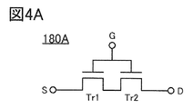
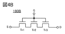
- 4A and 4B are diagrams showing circuit symbols of transistors.
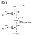
- 5A and 5B are diagrams illustrating a source follower circuit.
- FIG. 6 is a timing chart illustrating an operation example of the semiconductor device.
- 7A and 7B are diagrams for explaining an operation example of the semiconductor device.
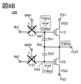
- 8A and 8B are diagrams for explaining an operation example of the semiconductor device.
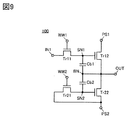
- FIG. 9 is a circuit diagram of a semiconductor device according to one aspect of the present invention.
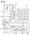
- FIG. 10A is a block diagram illustrating a configuration example of the semiconductor device.
- FIG. 10B is a perspective view of the semiconductor device.
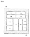
- FIG. 11 is a block diagram illustrating a CPU.
- 12A and 12B are perspective views of the semiconductor device.
- 13A and 13B are perspective views of the semiconductor device.
- 14A and 14B are perspective views of the semiconductor device.
- 15A and 15B are diagrams for explaining a configuration example of a neural network.
- FIG. 16 is a diagram showing a structural example of the semiconductor device.
- 17A to 17C are diagrams showing a configuration example of a transistor.
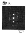
- FIG. 18A is a diagram for explaining the classification of the crystal structure of IGZO
- FIG. 18B is a diagram for explaining the XRD spectrum of crystalline IGZO
- FIG. 18A is a diagram for explaining the classification of the crystal structure of IGZO
- FIG. 18B is a diagram for explaining the XRD spectrum of crystalline IGZO
- FIG. 19B is a perspective view showing an example of a chip
- FIGS. 19C and 19D are perspective views showing an example of an electronic component.
- 20A to 20J are diagrams for explaining an example of an electronic device.
- 21A to 21E are diagrams illustrating an example of an electronic device.
- 22A to 22C are diagrams illustrating an example of an electronic device.
- 23A and 23B are diagrams according to an embodiment.
- FIG. 24 is a diagram according to an embodiment.
- FIG. 25 is a diagram according to an embodiment.
- the semiconductor device is a device utilizing semiconductor characteristics, and refers to a circuit including a semiconductor element (transistor, diode, photodiode, etc.), a device having the same circuit, and the like. It also refers to all devices that can function by utilizing semiconductor characteristics. For example, an integrated circuit, a chip having an integrated circuit, or an electronic component in which the chip is housed in a package is an example of a semiconductor device. Further, the storage device, the display device, the light emitting device, the lighting device, the electronic device, and the like are themselves semiconductor devices, and may have the semiconductor device.
- an element for example, a switch, a transistor, a capacitive element, an inductor, a resistance element, a diode, a display
- One or more devices, light emitting devices, loads, etc. can be connected between X and Y.
- the switch has a function of controlling the on state and the off state. That is, the switch is in a conducting state (on state) or a non-conducting state (off state), and has a function of controlling whether or not a current flows.
- a circuit that enables functional connection between X and Y for example, a logic circuit (inverter, NAND circuit, NOR circuit, etc.), signal conversion, etc.) Circuits (digital-analog conversion circuit, analog-digital conversion circuit, gamma correction circuit, etc.), potential level conversion circuit (power supply circuit (boost circuit, step-down circuit, etc.), level shifter circuit that changes the signal potential level, etc.), voltage source, current source , Switching circuit, amplifier circuit (circuit that can increase signal amplitude or current amount, operational amplifier, differential amplifier circuit, source follower circuit, buffer circuit, etc.), signal generation circuit, storage circuit, control circuit, etc.) It is possible to connect one or more to and from. As an example, even if another circuit is sandwiched between X and Y, if the signal output from X is transmitted to Y, it is assumed that X and Y are functionally connected. do.
- X and Y are electrically connected, it means that X and Y are electrically connected (that is, another element between X and Y). Or when they are connected with another circuit in between) and when X and Y are directly connected (that is, they are connected without another element or another circuit between X and Y). If there is) and.
- X and Y, the source (or the first terminal, etc.) and the drain (or the second terminal, etc.) of the transistor are electrically connected to each other, and the X, the source (or the second terminal, etc.) of the transistor are connected to each other. (1 terminal, etc.), the drain of the transistor (or the 2nd terminal, etc.), and Y are electrically connected in this order.
- the source of the transistor (or the first terminal, etc.) is electrically connected to X
- the drain of the transistor (or the second terminal, etc.) is electrically connected to Y
- the X, the source of the transistor (such as the second terminal).
- the first terminal, etc.), the drain of the transistor (or the second terminal, etc.), and Y are electrically connected in this order.
- X is electrically connected to Y via the source (or first terminal, etc.) and drain (or second terminal, etc.) of the transistor, and X, the source (or first terminal, etc.) of the transistor. (Terminals, etc.), transistor drains (or second terminals, etc.), and Y are provided in this connection order.
- the source (or first terminal, etc.) and drain (or second terminal, etc.) of the transistor can be separated. Separately, the technical scope can be determined. Note that these expression methods are examples, and are not limited to these expression methods.
- X and Y are assumed to be objects (for example, devices, elements, circuits, wirings, electrodes, terminals, conductive films, layers, etc.).
- circuit diagram shows that the independent components are electrically connected to each other, one component has the functions of a plurality of components.
- one component has the functions of a plurality of components.
- the term "electrically connected” as used herein includes the case where one conductive film has the functions of a plurality of components in combination.
- the “resistance element” can be, for example, a circuit element having a resistance value higher than 0 ⁇ , wiring, or the like. Therefore, in the present specification and the like, the “resistive element” includes a wiring having a resistance value, a transistor in which a current flows between a source and a drain, a diode, a coil, and the like. Therefore, the term “resistor element” can be paraphrased into terms such as “resistance”, “load”, and “region having resistance value”, and conversely, the terms “resistance”, “load”, and “region having resistance value” are used. , “Resistance element” and so on.
- the resistance value can be, for example, preferably 1 m ⁇ or more and 10 ⁇ or less, more preferably 5 m ⁇ or more and 5 ⁇ or less, and further preferably 10 m ⁇ or more and 1 ⁇ or less. Further, for example, it may be 1 ⁇ or more and 1 ⁇ 10 9 ⁇ or less.
- the “capacitance element” means, for example, a circuit element having a capacitance value higher than 0F, a wiring region having a capacitance value, a parasitic capacitance, a transistor gate capacitance, and the like. Can be. Therefore, in the present specification and the like, the “capacitive element” is not only a circuit element containing a pair of electrodes and a dielectric contained between the electrodes, but also a parasitic element appearing between the wirings. It shall include the capacitance, the gate capacitance that appears between the gate and one of the source or drain of the transistor, and so on.
- capacitor element in addition, terms such as “capacitive element”, “parasitic capacitance”, and “gate capacitance” can be paraphrased into terms such as “capacity”, and conversely, the term “capacity” refers to “capacitive element”, “parasitic capacitance”, and “capacity”. It can be paraphrased into terms such as “gate capacitance”.
- the term “pair of electrodes” of “capacity” can be paraphrased as “pair of conductors", “pair of conductive regions", “pair of regions” and the like.
- the value of the capacitance can be, for example, 0.05 fF or more and 10 pF or less. Further, for example, it may be 1 pF or more and 10 ⁇ F or less.
- the transistor has three terminals called a gate, a source, and a drain.
- the gate is a control terminal that controls the conduction state of the transistor.
- the two terminals that function as sources or drains are the input and output terminals of the transistor.
- One of the two input / output terminals becomes a source and the other becomes a drain depending on the high and low potentials given to the conductive type (n-channel type, p-channel type) of the transistor and the three terminals of the transistor. Therefore, in the present specification and the like, the terms source and drain can be paraphrased with each other.
- the transistor when explaining the connection relationship of transistors, "one of the source or drain” (or the first electrode or the first terminal), “the other of the source or drain” (or the second electrode, or The notation (second terminal) is used.
- it may have a back gate in addition to the above-mentioned three terminals.
- one of the gate or the back gate of the transistor may be referred to as a first gate
- the other of the gate or the back gate of the transistor may be referred to as a second gate.
- the terms “gate” and “backgate” may be interchangeable.
- the respective gates When the transistor has three or more gates, the respective gates may be referred to as a first gate, a second gate, a third gate, and the like in the present specification and the like.
- the “on current” may mean a current flowing between the source and the drain when the transistor is in the on state.
- the “off current” may mean a current flowing between the source and the drain when the transistor is in the off state.
- a node can be paraphrased as a terminal, a wiring, an electrode, a conductive layer, a conductor, an impurity region, or the like, depending on a circuit configuration and / or a device structure or the like.
- terminals, wiring, etc. can be paraphrased as nodes.
- ground potential ground potential
- the potentials are relative, and when the reference potential changes, the potential given to the wiring, the potential applied to the circuit or the like, the potential output from the circuit or the like also changes.
- the high power supply potential VDD (hereinafter, also simply referred to as “VDD”) indicates a power supply potential having a potential higher than that of the low power supply potential VSS (hereinafter, also simply referred to as “VSS”). Further, VSS indicates a power supply potential having a potential lower than VDD. Further, the ground potential (hereinafter, also simply referred to as “GND”) can be used as VDD or VSS. For example, when VDD is the ground potential, VSS is a potential lower than the ground potential, and when VSS is the ground potential, VDD is a potential higher than the ground potential.
- the "current” is a charge transfer phenomenon (electrical conduction).
- the description “electrical conduction of a positively charged body is occurring” means “electrical conduction of a negatively charged body in the opposite direction”. Is happening. " Therefore, in the present specification and the like, “current” refers to a charge transfer phenomenon (electrical conduction) accompanying the movement of carriers, unless otherwise specified.
- the carrier here include electrons, holes, anions, cations, complex ions, and the like, and the carriers differ depending on the system in which the current flows (for example, semiconductor, metal, electrolytic solution, vacuum, etc.).
- the "current direction” in the wiring or the like shall be the direction in which the positive carrier moves, and shall be described as a positive current amount.
- the direction in which the negative carrier moves is opposite to the direction of the current, and is expressed by the amount of negative current. Therefore, in the present specification and the like, if there is no notice about the positive or negative of the current (or the direction of the current), the description such as “current flows from element A to element B” means “current flows from element B to element A” or the like. It can be paraphrased as. Further, the description such as “a current is input to the element A” can be rephrased as "a current is output from the element A” or the like.
- the ordinal numbers “first”, “second”, and “third” are added to avoid confusion of the components. Therefore, the number of components is not limited. Moreover, the order of the components is not limited. For example, the component referred to in “first” in one of the embodiments of the present specification and the like may be the component referred to in “second” in another embodiment or in the claims. There can also be. Further, for example, the component mentioned in “first” in one of the embodiments of the present specification and the like may be omitted in another embodiment or in the claims.
- the terms “upper” and “lower” do not limit the positional relationship of the components to be directly above or directly below and to be in direct contact with each other.
- the terms “electrode B on the insulating layer A” it is not necessary that the electrode B is formed in direct contact with the insulating layer A, and another configuration is formed between the insulating layer A and the electrode B. Do not exclude those that contain elements.
- the positional relationship of the constituent elements changes as appropriate according to the direction in which each configuration is depicted. Therefore, it is not limited to the words and phrases explained in the specification and the like, and can be appropriately paraphrased according to the situation.
- terms indicating the arrangement such as “above” and “below” may be used for convenience in order to explain the positional relationship of the components with reference to the drawings. Therefore, in the expression of "insulator located on the upper surface of the conductor”, it can be rephrased as “insulator located on the lower surface of the conductor” by rotating the direction of the drawing shown by 180 degrees. Further, in the expression of "insulator located on the upper surface of the conductor”, it can be paraphrased as "insulator located on the left side (or right side) of the conductor” by rotating the direction of the drawing shown by 90 degrees. can.
- electrode B overlapping the insulating layer A is not limited to the state of "the electrode B is formed on the insulating layer A", but “the electrode B is formed under the insulating layer A”. It does not exclude the state of "being” or the state of "the electrode B is formed on the right side (or left side) of the insulating layer A”.
- the terms “adjacent” and “proximity” do not limit that the components are in direct contact with each other.
- electrode B adjacent to the insulating layer A it is not necessary that the insulating layer A and the electrode B are formed in direct contact with each other, and another component is formed between the insulating layer A and the electrode B. Do not exclude those that include.
- membrane and layer can be interchanged with each other depending on the situation.
- Electrode may be used as part of a “wiring” and vice versa.
- the terms “electrode” and “wiring” include the case where a plurality of “electrodes” and “wiring” are integrally formed.
- a “terminal” may be used as part of a “wiring” and an “electrode” and vice versa.
- the term “terminal” includes a case where a plurality of "electrodes", “wiring”, “terminals” and the like are integrally formed.
- the "electrode” can be a part of the “wiring” or the “terminal”, and for example, the “terminal” can be a part of the “wiring” or the “electrode”.
- terms such as “electrode”, “wiring”, and “terminal” may be replaced with terms such as "area” in some cases.
- wiring can be interchanged with each other in some cases or depending on the situation.
- “wiring”. It may be possible to change the term to the term “signal line”. Further, for example, it may be possible to change the term “wiring” to a term such as “power line”. The reverse is also true, and it may be possible to change terms such as “signal line” and “power supply line” to the term “wiring”.
- a term such as “power line” may be changed to a term such as "signal line”.
- terms such as “signal line” may be changed to terms such as "power line”.
- the term “potential” applied to the wiring may be changed to a term such as “signal” in some cases or depending on the situation. The reverse is also true, and terms such as “signal” may be changed to the term “potential”.
- semiconductor impurities refer to, for example, components other than the main components constituting the semiconductor layer.
- an element having a concentration of less than 0.1 atomic% is an impurity.
- the inclusion of impurities may result in, for example, an increase in the defect level density of the semiconductor, a decrease in carrier mobility, a decrease in crystallinity, and the like.
- the impurities that change the characteristics of the semiconductor include, for example, group 1 element, group 2 element, group 13 element, group 14 element, group 15 element, and other than the main component.
- transition metals and the like and in particular, hydrogen (also contained in water), lithium, sodium, silicon, boron, phosphorus, carbon, nitrogen and the like.
- the impurities that change the characteristics of the semiconductor include, for example, Group 1 elements other than oxygen and hydrogen, Group 2 elements, Group 13 elements, Group 15 elements, and the like. be.
- the switch means a switch that is in a conductive state (on state) or a non-conducting state (off state) and has a function of controlling whether or not a current flows.
- the switch means a switch having a function of selecting and switching a path through which a current flows.
- an electric switch, a mechanical switch, or the like can be used. That is, the switch is not limited to a specific switch as long as it can control the current.
- Examples of electrical switches include transistors (for example, bipolar transistors, MOS transistors, etc.), diodes (for example, PN diodes, PIN diodes, Schottky diodes, MIM (Metal Insulator Metal) diodes, and MIS (Metal Insulator Semiconductor) diodes. , Diode-connected transistors, etc.), or logic circuits that combine these.
- transistors for example, bipolar transistors, MOS transistors, etc.
- diodes for example, PN diodes, PIN diodes, Schottky diodes, MIM (Metal Insulator Metal) diodes, and MIS (Metal Insulator Semiconductor) diodes. , Diode-connected transistors, etc.
- the "conducting state (on state)" of the transistor means a state in which the source and drain of the transistor can be regarded as being electrically short-circuited.
- the "non-conducting state (off state)" of the transistor means a state in which the source and drain of the transistor can be regarded as being electrically cut off.
- the polarity (conductive type) of the transistor is not particularly limited.
- a mechanical switch is a switch using MEMS (Micro Electro Mechanical System) technology.
- the switch has an electrode that can be moved mechanically, and the movement of the electrode controls conduction and non-conduction.
- parallel means a state in which two straight lines are arranged at an angle of ⁇ 10 ° or more and 10 ° or less. Therefore, the case of ⁇ 5 ° or more and 5 ° or less is also included.
- substantially parallel or approximately parallel means a state in which two straight lines are arranged at an angle of ⁇ 30 ° or more and 30 ° or less.
- vertical means a state in which two straight lines are arranged at an angle of 80 ° or more and 100 ° or less. Therefore, the case of 85 ° or more and 95 ° or less is also included.
- substantially vertical or “approximately vertical” means a state in which two straight lines are arranged at an angle of 60 ° or more and 120 ° or less.
- a metal oxide is a metal oxide in a broad sense. Metal oxides are classified into oxide insulators, oxide conductors (including transparent oxide conductors), oxide semiconductors (also referred to as Oxide Semiconductor or simply OS) and the like. For example, when a metal oxide is used in the active layer of a transistor, the metal oxide may be referred to as an oxide semiconductor. That is, when a metal oxide can form a channel forming region of a transistor having at least one of an amplification action, a rectifying action, and a switching action, the metal oxide is referred to as a metal oxide semiconductor. be able to. Further, when describing as an OS transistor, it can be paraphrased as a transistor having a metal oxide or an oxide semiconductor.
- a metal oxide having nitrogen may also be collectively referred to as a metal oxide. Further, a metal oxide having nitrogen may be referred to as a metal oxynitride.
- the configuration shown in each embodiment can be appropriately combined with the configuration shown in other embodiments to form one aspect of the present invention. Further, when a plurality of configuration examples are shown in one embodiment, the configuration examples can be appropriately combined with each other.
- the content (may be a part of the content) described in one embodiment is the other content (may be a part of the content) described in the embodiment and one or more other implementations. It is possible to apply, combine, or replace at least one content with the content described in the form of (may be a part of the content).
- figure (which may be a part) described in one embodiment is different from another part of the figure, another figure (which may be a part) described in the embodiment, and one or more other figures.
- the figure (which may be a part) described in the embodiment is different from another part of the figure, another figure (which may be a part) described in the embodiment, and one or more other figures.
- more figures can be formed.
- the components are classified according to their functions and shown as blocks independent of each other.
- it is difficult to separate the components for each function and there may be a case where a plurality of functions are involved in one circuit or a case where one function is involved in a plurality of circuits. Therefore, the blocks in the block diagram are not limited to the components described in the specification, and can be appropriately paraphrased according to the situation.
- the size, layer thickness, or area may be exaggerated for clarity. Therefore, it is not necessarily limited to its size and aspect ratio.
- the drawings schematically show ideal examples, and are not limited to the shapes or values shown in the drawings. For example, it is possible to include variations in the signal, voltage, or current due to noise, or variations in the signal, voltage, or current due to timing lag.
- the code is used for identification such as "_1", “[n]", “[m, n]”. May be added and described.
- one of the two wiring GLs may be described as wiring GL [1], and the other may be described as wiring GL [2] or the like.
- FIG. 1A shows a circuit diagram of the semiconductor device 100 according to one aspect of the present invention.
- the semiconductor device 100 can function as a storage circuit capable of holding analog data. Further, the semiconductor device 100 can function as a storage element capable of holding analog data.
- the semiconductor device 100 includes a transistor Tr11, a transistor Tr12, a transistor Tr21, a transistor Tr22, a capacitive element Cb1, and a capacitive element Cb2.
- the semiconductor device 100 includes a holding circuit 110a, a holding circuit 110b, a bootstrap circuit 120a, a bootstrap circuit 120b, and a source follower circuit 130.
- the holding circuit 110a includes a transistor Tr11 and a capacitance element Cb1, and the holding circuit 110b includes a transistor Tr21 and a capacitance element Cb2.
- the bootstrap circuit 120a includes a transistor Tr12 and a capacitive element Cb1, and the bootstrap circuit 120b includes a transistor Tr22 and a capacitive element Cb2.
- the source follower circuit 130 includes a transistor Tr12 and a transistor Tr22.
- the gate of the transistor Tr11 is electrically connected to the terminal WW1, one of the source or drain of the transistor Tr11 is electrically connected to the terminal IN1, and the other is electrically connected to the gate of the transistor Tr12.
- One of the source or drain of the transistor Tr12 is electrically connected to the terminal PS1 and the other is electrically connected to the terminal OUT.
- the gate of the transistor Tr21 is electrically connected to the terminal WW2, one of the source or drain of the transistor Tr21 is electrically connected to the terminal IN2, and the other is electrically connected to the gate of the transistor Tr22.
- One of the source or drain of the transistor Tr22 is electrically connected to the terminal OUT, and the other is electrically connected to the terminal PS2.
- One electrode constituting the capacitive element Cb1 is electrically connected to the gate of the transistor Tr12, and the other electrode is electrically connected to the terminal OUT.
- One electrode constituting the capacitive element Cb2 is electrically connected to the terminal OUT, and the other electrode is electrically connected to the gate of the transistor Tr22.
- the node where the source or drain of the transistor Tr11, the gate of the transistor Tr12, and one of the electrodes constituting the capacitive element Cb1 are electrically connected functions as the node SN1.
- the node at which the source or drain of the transistor Tr21, the gate of the transistor Tr22, and the other electrode constituting the capacitive element Cb2 are electrically connected functions as the node SN2.
- the other electrode constituting the capacitance element Cb1, one electrode constituting the capacitance element Cb2, and the node electrically connected to the terminal OUT function as a node BN.
- the node SN1 and the node SN2 each function as a storage node.
- the holding circuit 110a has a function of holding the potential (charge) written in the node SN1 via the transistor Tr11.
- the holding circuit 110b has a function of holding the potential (charge) written in the node SN2 via the transistor Tr21.
- a potential for turning on the transistor Tr11 is supplied to the gate of the transistor Tr11, and an electric charge for making the node SN1 a predetermined potential is supplied to the node SN1 via the source and drain of the transistor Tr11. .. After that, a potential for turning off the transistor Tr11 is supplied to the gate of the transistor Tr11. By turning off the transistor Tr11, the electric charge written to the node SN1 is retained.
- a potential for turning on the transistor Tr21 is supplied to the gate of the transistor Tr21, and an electric charge for bringing the node SN2 to a predetermined potential is supplied to the node SN2 via the source and drain of the transistor Tr21. After that, a potential for turning off the transistor Tr21 is supplied to the gate of the transistor Tr21. By turning off the transistor Tr21, the electric charge written to the node SN2 is retained. Therefore, node SN1 and node SN2 are also referred to as "holding nodes”. Further, the transistor Tr11 and the transistor Tr21 are also referred to as "writing transistors”.
- a single crystal semiconductor, a polycrystalline semiconductor, a microcrystal semiconductor, an amorphous semiconductor, or the like can be used alone or in combination.
- the semiconductor material for example, silicon, germanium, or the like can be used. Further, compound semiconductors such as silicon germanium, silicon carbide, gallium arsenide, oxide semiconductors, and nitride semiconductors may be used.
- the semiconductor layer used for the transistor may be a stack of a plurality of semiconductor layers.
- semiconductors having different crystal states may be used, or different semiconductor materials may be used.
- the transistor Tr11 and the transistor Tr21 are preferably transistors (also referred to as "OS transistors") containing an oxide semiconductor in the semiconductor layer on which the channel is formed. Since the oxide semiconductor has a band gap of 2 eV or more, the off-current is remarkably small.
- OS transistors also referred to as "OS transistors”
- the electric charge written in the holding node can be held for a long period of time.
- the semiconductor device 100 can be called an "OS memory".
- the OS memory can retain the written information for a period of one year or more, or even ten years or more, even if the power supply is stopped. Therefore, the OS memory can be regarded as a non-volatile memory.
- the OS memory can hold not only binary information (1 bit) but also multi-value (multi-bit) information.
- the OS memory is a method of writing an electric charge to a node via an OS transistor, a high voltage required for a conventional flash memory is not required, and a high-speed writing operation can be realized. Further, the erasing operation before data rewriting performed in the flash memory is unnecessary in the OS memory. Also, since no charge is injected or withdrawn into the floating gate or charge capture layer, the OS memory can write and read data virtually unlimited times. The OS memory has less deterioration than the conventional flash memory, and high reliability can be obtained.
- the OS memory does not undergo a structural change at the atomic level like a magnetoresistive memory (MRAM) or a resistance change type memory (ReRAM). Therefore, the OS memory is superior in rewrite resistance to the magnetoresistive memory and the resistance change type memory.
- MRAM magnetoresistive memory
- ReRAM resistance change type memory
- the off-current of the OS transistor hardly increases even in a high temperature environment. Specifically, the off-current hardly increases even at an environmental temperature of room temperature or higher and 200 ° C. or lower. In addition, the on-current does not easily decrease even in a high temperature environment.
- the storage device including the OS memory has stable operation even in a high temperature environment, and high reliability can be obtained.
- the OS transistor has a high dielectric strength between the source and the drain. By using an OS transistor as a transistor constituting a semiconductor device, operation is stable even in a high temperature environment, and a semiconductor device with good reliability can be realized. Therefore, it is preferable to use an OS transistor for the transistor Tr11, the transistor Tr21, the transistor Tr12, and the transistor Tr22.
- the gate insulating film of the transistor Tr12 and the transistor Tr22 is extremely thin, the electric charge written to the node SN1 and the node SN2 may leak through the gate insulating film (also referred to as “gate leak”).
- the thickness of the gate insulating film of the transistor Tr12 and the transistor Tr22 is preferably about the same as the thickness of the gate insulating film of the transistor Tr11 and the transistor Tr21.
- an OS transistor may be used for the transistor Tr11 and the transistor Tr21
- a Si transistor may be used for the transistor Tr12 and the transistor Tr22.
- the Si transistor used for the transistor Tr12 and the transistor Tr22 a Si transistor having a structure with less gate leakage may be used.
- the data read speed can be increased by using the Si transistor for the transistor Tr12 and the transistor Tr22.
- the gate of the transistor Tr11 and the gate of the transistor Tr21 may be electrically connected to the wiring WWL.
- FIG. 2A shows an example in which the back gate of the transistor Tr12 is electrically connected to the terminal BG14 and the back gate of the transistor Tr22 is electrically connected to the terminal BG24.
- the threshold voltage of the transistor Tr12 can be changed.
- the threshold voltage of the transistor Tr22 can be changed.
- FIG. 2B shows an example in which the back gate of the transistor Tr11 is electrically connected to the terminal BG13 and the back gate of the transistor Tr21 is electrically connected to the terminal BG23.
- the threshold voltage of the transistor Tr11 can be changed.
- the threshold voltage of the transistor Tr21 can be changed.
- FIG. 3A shows an example in which a gate and a back gate are electrically connected in each of the transistor Tr11, the transistor Tr12, the transistor Tr21, and the transistor Tr22.
- FIG. 3B shows an example in which the back gate of the transistor Tr22 is electrically connected to the other of the source or drain of the transistor Tr22.
- each of the transistor Tr11, the transistor Tr12, the transistor Tr21, and the transistor Tr22 may be a double-gate type transistor.
- FIG. 4A shows an example of a circuit symbol of the double gate type transistor 180A.
- the transistor 180A has a configuration in which the transistor Tr1 and the transistor Tr2 are connected in series.
- one of the source or drain of the transistor Tr1 is electrically connected to the terminal S
- the other of the source or drain of the transistor Tr1 is electrically connected to one of the source or drain of the transistor Tr2, and the source of the transistor Tr2.
- the other side of the drain is electrically connected to the terminal D.
- FIG. 4A shows a state in which the gates of the transistor Tr1 and the transistor Tr2 are electrically connected and are electrically connected to the terminal G.
- the transistor 180A shown in FIG. 4A has a function of switching between the terminal S and the terminal D in a conductive state or a non-conducting state by changing the potential of the terminal G. Therefore, the transistor 180A, which is a double-gate type transistor, contains the transistor Tr1 and the transistor Tr2 and functions as one transistor. That is, in FIG. 4A, one of the source or drain of the transistor 180A is electrically connected to the terminal S, the other of the source or drain is electrically connected to the terminal D, and the gate is electrically connected to the terminal G. It can be said that there is.
- each of the transistor Tr11, the transistor Tr12, the transistor Tr21, and the transistor Tr22 may be a triple gate type transistor.
- FIG. 4B shows an example of a circuit symbol of the triple gate type transistor 180B.
- the transistor 180B has a configuration in which a transistor Tr1, a transistor Tr2, and a transistor Tr3 are connected in series.
- one of the source or drain of the transistor Tr1 is electrically connected to the terminal S
- the other of the source or drain of the transistor Tr1 is electrically connected to one of the source or drain of the transistor Tr2, and the source of the transistor Tr2.
- the other of the drains is electrically connected to one of the source or drain of the transistor Tr3, and the other of the source or drain of the transistor Tr3 is electrically connected to the terminal D.
- FIG. 4B shows a state in which the gates of the transistor Tr1, the transistor Tr2, and the transistor Tr3 are electrically connected and electrically connected to the terminal G.
- the transistor 180B shown in FIG. 4B has a function of switching between the terminal S and the terminal D in a conductive state or a non-conducting state by changing the potential of the terminal G. Therefore, the transistor 180B, which is a triple-gate type transistor, contains the transistor Tr1, the transistor Tr2, and the transistor Tr3, and functions as one transistor. That is, in FIG. 4B, one of the source or drain of the transistor 180B is electrically connected to the terminal S, the other of the source or drain is electrically connected to the terminal D, and the gate is electrically connected to the terminal G. It can be said that there is.
- a transistor having a plurality of gates and to which the plurality of gates are electrically connected such as the transistor 180A and the transistor 180B, may be referred to as a "multi-gate type transistor” or a “multi-gate transistor”.
- the semiconductor device 100 comprises the source follower circuit 130 by using the transistor Tr12 and the transistor Tr22.
- FIG. 5A is a circuit diagram of a source follower circuit 901 including a transistor M1 and a resistance element R1.
- the transistor M1 is an n-channel type transistor.
- the source of the transistor M1 is electrically connected to one terminal of the resistance element R1.
- VDD is supplied to the drain of the transistor M1
- VSS is supplied to the other terminal of the resistance element.
- the gate of the transistor M1 is electrically connected to the terminal IN, and the input voltage Vin is input via the terminal IN.
- the source of the transistor M1 is electrically connected to the terminal OUT, and the output voltage Vout is output via the terminal OUT.
- the transistors that make up the source follower circuit need to operate in the saturation region. Therefore, assuming that the threshold voltage of the transistor M1 is Vth, it is necessary to operate the transistor M1 under the condition satisfying the relationship of the equation 1.
- the output voltage Vout is the source voltage of the transistor M1
- the output voltage Vout is always approximately Vin minus Vth. More precisely, the output voltage Vout changes to satisfy Equation 2.
- Equation 2 mu n is the mobility, C OX denotes a gate capacitance, W is the channel width, L is channel length, Vin is (the gate voltage of the transistor M1) voltage input via the terminal IN, Vth is the transistors M1 The threshold voltage and R1 are resistance values of the resistance element R1.
- the output voltage Vout changes following the change of the input voltage Vin.
- the source follower circuit has a function of always supplying a constant voltage even if the input impedance of the load fluctuates. That is, the source follower circuit has a function of performing power amplification (amplifying the current value without changing the output voltage).
- the resistance element R1 of the source follower circuit 901 can be replaced with the transistor M2.
- the transistor M2 is an n-channel type transistor. Also in the source follower circuit 902, the transistor M1 and the transistor M2 are operated in the saturation region.
- the gate of the transistor M1 is electrically connected to the terminal IN1, and the gate of the transistor M2 is electrically connected to the terminal IN2.
- the drain of the transistor M2 is electrically connected to the terminal OUT. Further, a low power supply voltage VSS is supplied to the source of the transistor M2.
- the source follower circuit 902 also has a function of performing power amplification.
- Id1 the current flowing between the source and drain of the transistor M1 operating in the saturation region
- Id2 the current flowing between the source and drain of the transistor M2 operating in the saturation region
- Id1 is a mathematical formula 3
- Id2 is a mathematical formula. It can be represented by 4.
- Equation 3 ⁇ n is mobility, COX is gate capacitance, W is channel width, L is channel length, Vin1 is the voltage input via terminal IN1 (gate voltage of transistor M1), and Vth1 is transistor M1. The threshold voltage.
- Equation 4 ⁇ n is mobility, COX is gate capacitance, W is channel width, L is channel length, Vin2 is the voltage input via terminal IN2 (gate voltage of transistor M2), and Vth2 is transistor M2. The threshold voltage.
- the output voltage Vout of the source follower circuit 902 can be expressed by Equation 5.
- FIG. 6 is a timing chart for explaining the operation of the semiconductor device 100.
- 7 and 8 are diagrams for explaining the operating state of the semiconductor device 100.
- a symbol also referred to as “potential symbol” indicating a potential such as “VDD” or “VSS” may be written adjacent to a terminal, wiring, or the like. Further, in order to make it easier to understand the potential change of the terminal and the wiring, the potential symbol added to the terminal and the wiring where the potential has changed may be written in enclosing characters. In addition, an "x" symbol may be added over the transistor in the off state.
- the potentials of the terminals WW1 and WW2 are L potentials, and the potentials of the terminals PS1, terminal PS2, terminal IN1, terminal IN2, node SN1, node SN2, and terminal OUT are VSS. And.
- the potential at which the transistor can be turned off is referred to as L potential.
- the L potential may be VSS, for example, but does not mean a specific potential.
- the potential at which the transistor can be turned on is referred to as an H potential.
- the H potential may be, for example, VDD, but does not mean a specific potential.
- the H potential is supplied to the terminals WW1 and WW2 to turn on the transistor Tr11 and the transistor Tr21 (see FIG. 7A). Further, a voltage (Vdata + Vref) obtained by adding the reference voltage Vref (reference potential) to the data Vdata is supplied to the node SN1 via the terminal IN1 and the transistor Tr11.
- the L potential is supplied to the terminals WW1 and WW2 to turn off the transistor Tr11 and the transistor Tr21 (see FIG. 7B).
- the transistor Tr11 is turned off, the node SN1 is in a floating state, and the potential (charge) of the node SN1 is maintained.
- the transistor Tr21 is turned off, the node SN2 is in a floating state, and the potential (charge) of the node SN2 is maintained.
- FIG. 8A shows the state immediately after the start of the period T41.
- the potential of the node BN rises. Since the node SN1 is in a floating state during the period T41 and is capacitively coupled to the node BN via the capacitive element Cb1, the potential of the node SN1 (also referred to as “Vsn1”) also rises due to the bootstrap effect. Similarly, since the node SN2 is in a floating state during the period T41 and the node SN2 is capacitively coupled to the node BN via the capacitive element Cb2, the potential of the node SN2 (also referred to as “Vsn2”) is also increased by the bootstrap effect. Ascend (see FIG. 8B).
- the semiconductor device 100 has a bootstrap circuit 120a including the transistor Tr12 and the capacitive element Cb1.
- the bootstrap circuit 120a has a function of boosting the potential of the node SN1.
- the semiconductor device 100 has a bootstrap circuit 120b including a transistor Tr22 and a capacitive element Cb2.
- the bootstrap circuit 120b has a function of boosting the potential of the node SN2.
- the potential of the node BN can be read as the output voltage Vout.
- the potential of the node BN (output voltage Vout) becomes a potential corresponding to the potential difference between the node SN1 and the node SN2. Further, the potential of the node BN (output voltage Vout) changes until the above-mentioned equation 5 is satisfied. Specifically, it changes until it becomes Vsn1-Vsn2. Therefore, the potential of the node BN (output voltage Vout) finally becomes Vdata.
- one of the source and drain of the transistor Tr21 that is electrically connected to the terminal IN2 may be electrically connected to the terminal PS2 instead of the terminal IN2.
- the semiconductor device 100 has a function of holding analog data and a function of power-amplifying and outputting the holding analog data. Since the held data is power-amplified at the time of reading, it is possible to eliminate the need for a power amplification circuit or the like used after reading the data. Alternatively, the quantity or scale of the power amplifier circuit can be reduced.
- the semiconductor device 100 can stably output (read) the retained data even if the impedance of the load connected to the output terminal (terminal OUT) fluctuates.
- the semiconductor device 100 according to one aspect of the present invention can hold not only analog data but also digital data.
- FIG. 10A shows a block diagram showing a configuration example of the semiconductor device 400.
- the semiconductor device 400 shown in FIG. 10A includes a drive circuit 410 and a memory array 420.
- the memory array 420 has a plurality of semiconductor devices 100.
- the semiconductor device 100 functions as a memory cell.
- FIG. 10A shows an example in which the memory array 420 has a plurality of semiconductor devices 100 arranged in a matrix.
- the drive circuit 410 includes a PSW241 (power switch), a PSW242, and a peripheral circuit 415.
- the peripheral circuit 415 includes a peripheral circuit 411, a control circuit 412 (Control Circuit), and a voltage generation circuit 428.
- each circuit, each signal, and each voltage can be appropriately discarded as needed. Alternatively, other circuits or other signals may be added.
- the signals BW, CE, GW, CLK, WAKE, ADDR, WDA, PON1 and PON2 are input signals from the outside, and the signal RDA is an output signal to the outside.
- the signal CLK is a clock signal.
- the signals BW, CE, and signal GW are control signals.
- the signal CE is a chip enable signal
- the signal GW is a global write enable signal
- the signal BW is a byte write enable signal.
- the signal ADDR is an address signal.
- the signal WDA is write data and the signal RDA is read data.
- the signals PON1 and PON2 are power gating control signals.
- the signals PON1 and PON2 may be generated by the control circuit 412.
- the control circuit 412 is a logic circuit having a function of controlling the overall operation of the semiconductor device 400. For example, the control circuit logically performs a signal CE, a signal GW, and a signal BW to determine an operation mode (for example, a write operation and a read operation) of the semiconductor device 400. Alternatively, the control circuit 412 generates a control signal of the peripheral circuit 411 so that this operation mode is executed.
- the voltage generation circuit 428 has a function of generating a negative voltage.
- WAKE has a function of controlling the input of CLK to the voltage generation circuit 428. For example, when an H level signal is given to WAKE, the signal CLK is input to the voltage generation circuit 428, and the voltage generation circuit 428 generates a negative voltage.
- the peripheral circuit 411 is a circuit for writing and reading data to and from the semiconductor device 100.
- the peripheral circuit 411 includes a row decoder 441 (Low Decoder), a column decoder 442 (Column Decoder), a row driver 423 (Low Driver), a column driver 424 (Color Driver), an input circuit 425 (Input Cir.), And an output circuit 426 (Output Circuit). It has Output Cir.). If necessary, a sense amplifier or the like may be provided.
- the row decoder 441 and the column decoder 442 have a function of decoding the signal ADDR.
- the row decoder 441 is a circuit for designating the row to be accessed
- the column decoder 442 is a circuit for designating the column to be accessed.
- the row driver 423 has a function of selecting the wiring specified by the row decoder 441.
- the column driver 424 has a function of writing data to the semiconductor device 100, a function of reading data from the semiconductor device 100, a function of holding the read data, and the like.
- the input circuit 425 has a function of holding the signal WDA.
- the data held by the input circuit 425 is output to the column driver 424.
- the output data of the input circuit 425 is the data (Din) to be written in the semiconductor device 100.
- the data (Dout) read from the semiconductor device 100 by the column driver 424 is output to the output circuit 426.
- the output circuit 426 has a function of holding the Dout. Further, the output circuit 426 has a function of outputting the Dout to the outside of the semiconductor device 400.
- the data output from the output circuit 426 is the signal RDA.
- the PSW241 has a function of controlling the supply of VDD to the peripheral circuit 415.
- the PSW242 has a function of controlling the supply of VHM to the row driver 423.
- the high power supply voltage of the semiconductor device 400 is VDD
- the low power supply voltage is GND (ground potential).
- VHM is a high power supply voltage used to raise the word line to a high level, which is higher than VDD.
- the signal PON1 controls the on / off of the PSW241, and the signal PON2 controls the on / off of the PSW242.
- the number of power supply domains to which VDD is supplied in the peripheral circuit 415 is set to 1, but it can be set to a plurality. In this case, a power switch may be provided for each power supply domain.
- the drive circuit 410 and the memory array 420 included in the semiconductor device 400 may be provided on the same plane. Further, as shown in FIG. 10B, the drive circuit 410 and the memory array 420 may be provided in an overlapping manner. By providing the drive circuit 410 and the memory array 420 in an overlapping manner, the signal propagation distance can be shortened.
- the semiconductor device 400 may use an arithmetic processing unit such as a CPU (Central Processing Unit) and / or a GPU (Graphics Processing Unit) for the control circuit 412 included in the drive circuit 410.
- an arithmetic processing unit such as a CPU (Central Processing Unit) and / or a GPU (Graphics Processing Unit)
- CPU Central Processing Unit
- GPU Graphics Processing Unit
- FIG. 11 shows a block diagram of the arithmetic processing unit 1100.
- FIG. 11 shows a CPU configuration example as a configuration example that can be used in the arithmetic processing device 1100.
- the arithmetic processing unit 1100 shown in FIG. 11 has an ALU 1191 (ALU: Arithmetic logic unit, arithmetic circuit), an ALU controller 1192, an instruction decoder 1193, an interrupt controller 1194, a timing controller 1195, a register 1196, and a register controller 1197 on a substrate 1190. It has a bus interface 1198), a cache 1199, and a cache interface 1189.
- ALU 1191 Arithmetic logic unit, arithmetic circuit
- ALU controller 1192 Arithmetic logic unit, arithmetic circuit
- an instruction decoder 1193 an instruction decoder 1193
- an interrupt controller 1194 a timing controller 1195, a register 1196, and a register controller 1197 on a substrate 1190.
- a bus interface 1198 As the substrate 1190, a semiconductor substrate, an SOI substrate, a glass substrate, or the like is used. It may have a rewritable ROM and a ROM interface.
- the cache 1199 is connected to the main memory provided on another chip via the cache interface 1189.
- the cache interface 1189 has a function of supplying a part of the data held in the main memory to the cache 1199.
- the cache 1199 has a function of holding the data.
- the arithmetic processing unit 1100 shown in FIG. 11 is only an example showing a simplified configuration thereof, and the actual arithmetic processing unit 1100 has a wide variety of configurations depending on its use.
- a configuration including the arithmetic processing unit 1100 shown in FIG. 11 or an arithmetic circuit may be used as one core, and a plurality of the cores may be included so that each core operates in parallel, that is, a configuration such as a GPU.
- the number of bits that the arithmetic processing device 1100 can handle in the internal arithmetic circuit and the data bus can be, for example, 8 bits, 16 bits, 32 bits, 64 bits, or the like.
- the instructions input to the arithmetic processing unit 1100 via the bus interface 1198 are input to the instruction decoder 1193, decoded, and then input to the ALU controller 1192, the interrupt controller 1194, the register controller 1197, and the timing controller 1195.
- the ALU controller 1192, the interrupt controller 1194, the register controller 1197, and the timing controller 1195 perform various controls based on the decoded instructions. Specifically, the ALU controller 1192 generates a signal for controlling the operation of the ALU 1191. Further, the interrupt controller 1194 determines and processes an interrupt request from an external input / output device or a peripheral circuit based on its priority and mask state during program execution of the arithmetic processing unit 1100. The register controller 1197 generates the address of the register 1196, and reads and writes the register 1196 according to the state of the arithmetic processing unit 1100.
- the timing controller 1195 generates a signal for controlling the operation timing of the ALU 1191, the ALU controller 1192, the instruction decoder 1193, the interrupt controller 1194, and the register controller 1197.
- the timing controller 1195 includes an internal clock generator that generates an internal clock signal based on the reference clock signal, and supplies the internal clock signal to the above-mentioned various circuits.
- a storage device is provided in the register 1196 and the cache 1199.
- the storage device for example, the semiconductor device 100 shown in the above embodiment may be used.
- the register controller 1197 selects the holding operation in the register 1196 according to the instruction from the ALU 1191. That is, in the memory cell of the register 1196, it is selected whether to hold the data by the flip-flop or the data by the capacitive element. When the holding of data by the flip-flop is selected, the power supply voltage is supplied to the memory cell in the register 1196. When the retention of data in the capacitive element is selected, the data is rewritten to the capacitive element, and the supply of the power supply voltage to the memory cell in the register 1196 can be stopped.
- the arithmetic processing unit 1100 is not limited to the CPU, and may be a GPU, a DSP (Digital Signal Processor), an FPGA (Field-Programmable Gate Array), or the like.
- the semiconductor device 400 and the arithmetic processing unit 1100 shown in the above embodiment can be provided in an overlapping manner.
- 12A and 12B show perspective views of the semiconductor device 1150A.
- the semiconductor device 1150A has a semiconductor device 400 that functions as a storage device on the arithmetic processing unit 1100.
- the arithmetic processing unit 1100 and the semiconductor device 400 have regions that overlap each other. In order to make the configuration of the semiconductor device 1150A easy to understand, the arithmetic processing unit 1100 and the semiconductor device 400 are shown separately in FIG. 12B.
- connection distance between the two can be shortened. Therefore, the communication speed between the two can be increased. Moreover, since the connection distance is short, power consumption can be reduced.
- FIG. 13A and 13B show perspective views of the semiconductor device 1150B.
- the semiconductor device 1150B has a semiconductor device 400a and a semiconductor device 400b on the arithmetic processing unit 1100.
- the arithmetic processing unit 1100, the semiconductor device 400a, and the semiconductor device 400b have regions that overlap each other.
- FIG. 13B shows the arithmetic processing unit 1100, the semiconductor device 400a, and the semiconductor device 400b separately.
- the semiconductor device 400a and the semiconductor device 400b function as a storage device.
- a NOR type storage device may be used for one of the semiconductor device 400a or the semiconductor device 400b, and a NAND type storage device may be used for the other.
- Both the semiconductor device 400a and the semiconductor device 400b may be a NAND type storage device or a NOR type storage device.
- the NOR type storage device includes DRAM, SRAM, and the like. Since the NOR type storage device can operate at a higher speed than the NAND type storage device, for example, a part of the semiconductor device 400a can be used as the main memory and / or the cache 1199.
- the stacking order of the semiconductor device 400a and the semiconductor device 400b may be reversed.
- FIG. 14A and 14B are perspective views of the semiconductor device 1150C.
- the semiconductor device 1150C has a configuration in which the arithmetic processing unit 1100 is sandwiched between the semiconductor device 400a and the semiconductor device 400b.
- the arithmetic processing unit 1100, the semiconductor device 400a, and the semiconductor device 400b have regions that overlap each other.
- FIG. 14B shows the arithmetic processing unit 1100, the semiconductor device 400a, and the semiconductor device 400b separately.
- both the communication speed between the semiconductor device 400a and the arithmetic processing device 1100 and the communication speed between the semiconductor device 400b and the arithmetic processing device 1100 can be increased. Moreover, the power consumption can be reduced as compared with the semiconductor device 1150B.
- the semiconductor device according to one aspect of the present invention can be used for an artificial neural network.
- An example of the configuration of the artificial neural network will be described below.
- FIG. 15A shows a configuration example of the neural network NN.
- the neural network NN can be composed of an input layer IL, an output layer OL, and an intermediate layer (hidden layer) HL.
- the input layer IL, the output layer OL, and the intermediate layer HL each have one or more neurons (units).
- the intermediate layer HL may be one layer or two or more layers.
- a neural network having two or more intermediate layers HL can also be called a DNN (deep neural network), and learning using a deep neural network can also be called deep learning.
- Input data is input to each neuron in the input layer IL, the output signal of the anterior layer or posterior layer neuron is input to each neuron in the intermediate layer HL, and the output of the anterior layer neuron is input to each neuron in the output layer OL.
- the signal is input.
- Each neuron may be connected to all neurons in the anterior and posterior layers (fully connected), or may be connected to some neurons.
- FIG. 15B shows an example of operation by neurons.
- two neurons in the presheaf layer that output a signal to the neuron N are shown.
- the output x 1 of the presheaf neuron and the output x 2 of the presheaf neuron are input to the neuron N.
- the sum of the multiplication result of the output x 1 and the weight w 1 (x 1 w 1 ) and the multiplication result of the output x 2 and the weight w 2 (x 2 w 2 ) is x 1 w 1 + x 2 w 2.
- the operation by the neuron includes the operation of adding the product of the output of the neuron in the previous layer and the weight, that is, the product-sum operation (x 1 w 1 + x 2 w 2 above ).
- This product-sum operation may be performed by software using a program or by hardware.
- a product-sum calculation circuit can be used.
- the product-sum calculation circuit a digital circuit or an analog circuit may be used.
- the processing speed can be improved and the power consumption can be reduced by reducing the circuit scale of the product-sum calculation circuit or reducing the number of times the memory is accessed.
- analog data is used as weight information.
- the semiconductor device 100 can hold analog data without converting it into a digital value. Therefore, conversion circuits such as DAC (Digital to Analog Converter) and / or ADC (Analog to Digital Converter) can be reduced, and power consumption and occupied area can be reduced.
- DAC Digital to Analog Converter
- ADC Analog to Digital Converter
- FIG. 16 A part of the cross-sectional structure of the semiconductor device is shown in FIG.
- the semiconductor device shown in FIG. 16 includes a transistor 550, a transistor 500, and a capacitive element 600.
- FIG. 17A is a top view of the transistor 500.
- FIG. 17B is a cross-sectional view of the portion L1-L2 shown by the alternate long and short dash line in FIG. 17A, and is a cross-sectional view of the transistor 500 in the channel length direction.
- FIG. 17C is a cross-sectional view of the portion W1-W2 shown by the alternate long and short dash line in FIG. 17A, and is a cross-sectional view of the transistor 500 in the channel width direction.
- the transistor 500 corresponds to an OS transistor included in the semiconductor device 100 shown in the above embodiment, that is, a transistor having an oxide semiconductor in a channel forming region.
- the transistor 550 corresponds to a Si transistor included in the drive circuit 410 shown in the above embodiment, that is, a transistor having silicon in the channel forming region.
- the transistor 500 is an OS transistor.
- the OS transistor has an extremely small off current. Therefore, it is possible to hold the data voltage or electric charge written to the storage node via the transistor 500 for a long period of time. That is, since the refresh operation frequency of the storage node is reduced or the refresh operation is not required, the power consumption of the semiconductor device can be reduced.
- the transistor 500 is provided above the transistor 550, and the capacitive element 600 is provided above the transistor 550 and the transistor 500.
- the transistor 550 is provided on the substrate 371.
- the substrate 371 is, for example, a p-type silicon substrate.
- the substrate 371 may be an n-type silicon substrate.
- the oxide layer 374 is preferably an insulating layer (also referred to as a BOX layer) formed by an embedded oxide (Burried oxide) in the substrate 371, for example, silicon oxide.
- the transistor 550 is provided on a single crystal silicon, so-called SOI (Silicon On Insulator) substrate, which is provided on the substrate 371 via an oxide layer 374.
- SOI Silicon On Insulator
- the substrate 371 of the SOI substrate is provided with an insulator 373 that functions as an element separation layer.
- the substrate 371 also has a well region 372.
- the well region 372 is a region to which n-type or p-type conductivity is imparted depending on the conductivity type of the transistor 550.
- the single crystal silicon in the SOI substrate is provided with a semiconductor region 375, a low resistance region 376a that functions as a source region or a drain region, and a low resistance region 376b. Further, a low resistance region 376c is provided on the well region 372.
- the transistor 550 can be provided so as to be superposed on the well region 372 to which the impurity element that imparts conductivity is added.
- the well region 372 can function as a bottom gate electrode of the transistor 550 by independently changing the potential via the low resistance region 376c. Therefore, the threshold voltage of the transistor 550 can be controlled.
- the threshold voltage of the transistor 550 can be made larger and the off-current can be reduced. Therefore, by applying a negative potential to the well region 372, the drain current when the potential applied to the gate electrode of the Si transistor is 0 V can be reduced. As a result, the power consumption based on the through current or the like in the arithmetic circuit having the transistor 550 can be reduced, and the arithmetic efficiency can be improved.
- the transistor 550 is preferably of the so-called Fin type, in which the upper surface of the semiconductor layer and the side surface in the channel width direction are covered with the conductor 378 via the insulator 377.
- the on-characteristics of the transistor 550 can be improved by increasing the effective channel width. Further, since the contribution of the electric field of the gate electrode can be increased, the off characteristic of the transistor 550 can be improved.
- the transistor 550 may be either a p-channel type transistor or an n-channel type transistor.
- the conductor 378 may function as a first gate (also referred to as a top gate) electrode. Further, the well region 372 may function as a second gate (also referred to as a bottom gate) electrode. In that case, the potential applied to the well region 372 can be controlled via the low resistance region 376c.
- the low resistance region 376a which is the region where the channel of the semiconductor region 375 is formed, the region in the vicinity thereof, the source region, or the drain region, and the low resistance region 376b, which is connected to the electrode controlling the potential of the well region 372.
- the region 376c or the like preferably contains a semiconductor such as a silicon-based semiconductor, and preferably contains single crystal silicon. Alternatively, it may be formed of a material having Ge (germanium), SiGe (silicon germanium), GaAs (gallium arsenide), GaAlAs (gallium aluminum arsenide), or the like. A configuration using silicon in which the effective mass is controlled by applying stress to the crystal lattice and changing the lattice spacing may be used. Alternatively, the transistor 550 may be a HEMT by using GaAs, GaAlAs, or the like.
- the well region 372, the low resistance region 376a, the low resistance region 376b, and the low resistance region 376c are elements that impart n-type conductivity such as arsenic and phosphorus, or boron, in addition to the semiconductor material applied to the semiconductor region 375. It contains an element that imparts p-type conductivity such as.
- the conductor 378 that functions as a gate electrode is a semiconductor material such as silicon, a metal material, or an alloy that contains an element that imparts n-type conductivity such as arsenic or phosphorus, or an element that imparts p-type conductivity such as boron.
- a material or a conductive material such as a metal oxide material can be used.
- a silicide such as nickel silicide may be used as the conductor 378.
- the threshold voltage of the transistor can be adjusted by selecting the material of the conductor. Specifically, it is preferable to use a material such as titanium nitride or tantalum nitride for the conductor. Further, in order to achieve both conductivity and embedding property, it is preferable to use a metal material such as tungsten or aluminum as a laminate for the conductor, and it is particularly preferable to use tungsten in terms of heat resistance.
- the low resistance region 376a, the low resistance region 376b, and the low resistance region 376c may be configured to be provided by laminating another conductor, for example, a silicide such as nickel silicide. With this configuration, the conductivity of the region that functions as an electrode can be enhanced. At this time, an insulator that functions as a side wall spacer (also referred to as a side wall insulating layer) may be provided on the side surface of the conductor 378 that functions as the gate electrode and the side surface of the insulator that functions as the gate insulating film. .. With this configuration, it is possible to prevent the conductor 378 and the low resistance region 376a and the low resistance region 376b from being in a conductive state.
- a silicide such as nickel silicide
- An insulator 379, an insulator 381, an insulator 383, and an insulator 385 are laminated in this order so as to cover the transistor 550.
- the insulator 379, the insulator 381, the insulator 383, and the insulator 385 for example, silicon oxide, silicon oxide, silicon nitride, silicon nitride, aluminum oxide, aluminum oxide, aluminum nitride, aluminum nitride, etc. are used. Just do it.
- silicon oxide refers to a material having a higher oxygen content than nitrogen as its composition
- silicon nitride as its composition means a material having a higher nitrogen content than oxygen as its composition. Is shown.
- aluminum nitride refers to a material whose composition has a higher oxygen content than nitrogen
- aluminum nitride refers to a material whose composition has a higher nitrogen content than oxygen. Is shown.
- the insulator 381 may have a function as a flattening film for flattening a step generated by a transistor 550 or the like provided below the insulator 381.
- the upper surface of the insulator 381 may be flattened by a flattening treatment using a chemical mechanical polishing (CMP) method or the like in order to improve the flatness.
- CMP chemical mechanical polishing
- the insulator 383 it is preferable to use a film having a barrier property so that hydrogen and impurities do not diffuse in the region where the transistor 500 is provided from the substrate 371 or the transistor 550.
- a film having a barrier property against hydrogen for example, silicon nitride formed by the CVD method can be used.
- hydrogen may diffuse into a semiconductor element having an oxide semiconductor such as a transistor 500, so that the characteristics of the semiconductor element may deteriorate. Therefore, it is preferable to use a film that suppresses the diffusion of hydrogen between the transistor 500 and the transistor 550.
- the membrane that suppresses the diffusion of hydrogen is a membrane that desorbs a small amount of hydrogen.
- the amount of hydrogen desorbed can be analyzed using, for example, a heated desorption gas analysis method (TDS).
- TDS heated desorption gas analysis method
- the amount of hydrogen desorbed from the insulator 383 is such that the amount desorbed in terms of hydrogen atoms is converted per area of the insulator 383 when the surface temperature of the film is in the range of 50 ° C. to 500 ° C. It may be 10 ⁇ 10 15 atoms / cm 2 or less, preferably 5 ⁇ 10 15 atoms / cm 2 or less.
- the insulator 385 preferably has a lower dielectric constant than the insulator 383.
- the relative permittivity of the insulator 385 is preferably less than 4, more preferably less than 3.
- the relative permittivity of the insulator 385 is preferably 0.7 times or less, more preferably 0.6 times or less, the relative permittivity of the insulator 383.
- the insulator 379, the insulator 381, the insulator 383, and the insulator 385 are embedded with a capacitance element 600, a conductor 328 connected to the transistor 500, a conductor 330, and the like.
- the conductor 328 and the conductor 330 have a function as a plug or a wiring.
- the conductor having a function as a plug or a wiring may collectively give a plurality of configurations and give the same reference numeral.
- the wiring and the plug connected to the wiring may be integrated. That is, a part of the conductor may function as a wiring, and a part of the conductor may function as a plug.
- each plug and wiring As the material of each plug and wiring (conductor 328, conductor 330, etc.), a conductive material such as a metal material, an alloy material, a metal nitride material, or a metal oxide material is used as a single layer or laminated. be able to. It is preferable to use a refractory material such as tungsten or molybdenum that has both heat resistance and conductivity, and it is preferable to use tungsten. Alternatively, it is preferably formed of a low resistance conductive material such as aluminum or copper. Wiring resistance can be reduced by using a low resistance conductive material.
- a wiring layer may be provided on the insulator 385 and the conductor 330.
- the insulator 350, the insulator 352, and the insulator 354 are laminated in this order.
- a conductor 356 is formed on the insulator 350, the insulator 352, and the insulator 354.
- the conductor 356 has a function as a plug or wiring for connecting to the transistor 550.
- the conductor 356 can be provided by using the same materials as the conductor 328 and the conductor 330.
- the insulator 350 it is preferable to use an insulator having a barrier property against hydrogen, similarly to the insulator 383.
- the conductor 356 preferably contains a conductor having a barrier property against hydrogen.
- a conductor having a barrier property against hydrogen is formed in the opening of the insulator 350 having a barrier property against hydrogen.
- the conductor having a barrier property against hydrogen for example, tantalum nitride or the like may be used. Further, by laminating tantalum nitride and tungsten having high conductivity, it is possible to suppress the diffusion of hydrogen from the transistor 550 while maintaining the conductivity as wiring. In this case, it is preferable that the tantalum nitride layer having a barrier property against hydrogen is in contact with the insulator 350 having a barrier property against hydrogen.
- a wiring layer may be provided on the insulator 354 and the conductor 356.
- the insulator 360, the insulator 362, and the insulator 364 are laminated in this order.
- a conductor 366 is formed in the insulator 360, the insulator 362, and the insulator 364.
- the conductor 366 has a function as a plug or wiring.
- the conductor 366 can be provided by using the same materials as the conductor 328 and the conductor 330.
- the insulator 360 it is preferable to use an insulator having a barrier property against hydrogen, similarly to the insulator 383.
- the conductor 366 preferably contains a conductor having a barrier property against hydrogen.
- a conductor having a barrier property against hydrogen is formed in the opening of the insulator 360 having a barrier property against hydrogen.
- a wiring layer may be provided on the insulator 364 and the conductor 366.
- the insulator 370, the insulator 369, and the insulator 368 are laminated in this order.
- a conductor 376 is formed on the insulator 370, the insulator 369, and the insulator 368.
- the conductor 376 has a function as a plug or wiring.
- the conductor 376 can be provided by using the same materials as the conductor 328 and the conductor 330.
- the insulator 370 it is preferable to use an insulator having a barrier property against hydrogen, similarly to the insulator 383.
- the conductor 376 preferably contains a conductor having a barrier property against hydrogen.
- a conductor having a barrier property against hydrogen is formed in the opening of the insulator 370 having a barrier property against hydrogen.
- a wiring layer may be provided on the insulator 368 and the conductor 376.
- the insulator 380, the insulator 382, and the insulator 384 are laminated in this order.
- a conductor 386 is formed on the insulator 380, the insulator 382, and the insulator 384.
- the conductor 386 has a function as a plug or wiring.
- the conductor 386 can be provided by using the same materials as the conductor 328 and the conductor 330.
- the insulator 380 it is preferable to use an insulator having a barrier property against hydrogen, similarly to the insulator 383.
- the conductor 386 preferably contains a conductor having a barrier property against hydrogen.
- a conductor having a barrier property against hydrogen is formed in the opening of the insulator 380 having a barrier property against hydrogen.
- the semiconductor device according to the present embodiment has been described. It is not limited to this.
- the number of wiring layers similar to the wiring layer containing the conductor 356 may be three or less, or the number of wiring layers similar to the wiring layer containing the conductor 356 may be five or more.
- An insulator 510, an insulator 512, an insulator 514, and an insulator 516 are laminated in this order on the insulator 384.
- any of the insulator 510, the insulator 512, the insulator 514, and the insulator 516 it is preferable to use a substance having a barrier property against oxygen and hydrogen.
- the insulator 510 and the insulator 514 it is preferable to use a film having a barrier property against hydrogen and impurities in the region where the transistor 500 is provided, for example, from the region where the substrate 371 or the transistor 550 is provided. Therefore, the same material as the insulator 383 can be used.
- silicon nitride formed by the CVD method can be used as an example of a film having a barrier property against hydrogen.
- hydrogen may diffuse into a semiconductor element having an oxide semiconductor such as a transistor 500, so that the characteristics of the semiconductor element may deteriorate. Therefore, it is preferable to use a film that suppresses the diffusion of hydrogen between the transistor 500 and the transistor 550.
- the film having a barrier property against hydrogen for example, it is preferable to use metal oxides such as aluminum oxide, hafnium oxide, and tantalum oxide for the insulator 510 and the insulator 514.
- metal oxides such as aluminum oxide, hafnium oxide, and tantalum oxide for the insulator 510 and the insulator 514.
- aluminum oxide has a high blocking effect that does not allow the membrane to permeate both oxygen and impurities such as hydrogen and water that cause fluctuations in the electrical characteristics of the transistor. Therefore, aluminum oxide can prevent impurities such as hydrogen and moisture from being mixed into the transistor 500 during and after the manufacturing process of the transistor. In addition, it is possible to suppress the release of oxygen from the oxides constituting the transistor 500. Therefore, it is suitable for use as a protective film for the transistor 500.
- the same material as the insulator 379 can be used for the insulator 512 and the insulator 516. Further, by applying a material having a relatively low dielectric constant to these insulators, it is possible to reduce the parasitic capacitance generated between the wirings.
- a silicon oxide film, a silicon nitride film, or the like can be used as the insulator 512 and the insulator 516.
- the insulator 510, the insulator 512, the insulator 514, and the insulator 516 are embedded with a conductor 518, a conductor (for example, a conductor 503) constituting the transistor 500, and the like.
- the conductor 518 has a function as a plug or wiring for connecting to the capacitance element 600 or the transistor 550.
- the conductor 518 can be provided by using the same material as the conductor 328 and the conductor 330.
- the conductor 510 and the conductor 518 in the region in contact with the insulator 514 are preferably conductors having a barrier property against oxygen, hydrogen, and water.
- the transistor 550 and the transistor 500 can be separated by a layer having a barrier property against oxygen, hydrogen, and water, and the diffusion of hydrogen from the transistor 550 to the transistor 500 can be suppressed.
- a transistor 500 is provided above the insulator 516.
- the transistor 500 has a conductor 503 arranged so as to be embedded in the insulator 514 and the insulator 516, and an insulator 520 arranged on the insulator 516 and the insulator 503.
- the insulator 524 placed on the insulator 522, the oxide 530a placed on the insulator 524, and the oxide 530a.
- the arranged oxide 530b, the conductors 542a and 542b arranged apart from each other on the oxide 530b, and the conductors 542a and 542b are arranged between the conductors 542a and 542b.
- It has an insulator 580 on which an opening is formed by superimposing, an insulator 545 arranged on the bottom surface and side surfaces of the opening, and a conductor 560 arranged on the forming surface of the insulator 545.
- the insulator 544 is arranged between the oxide 530a, the oxide 530b, the conductor 542a, and the conductor 542b and the insulator 580.
- the conductor 560 includes a conductor 560a provided inside the insulator 545 and a conductor 560b provided so as to be embedded inside the conductor 560a. It is preferable to have.
- the insulator 574 is arranged on the insulator 580, the conductor 560, and the insulator 545.
- oxide 530a and oxide 530b may be collectively referred to as oxide 530.
- the transistor 500 shows a configuration in which two layers of oxide 530a and oxide 530b are laminated in a region where a channel is formed and in the vicinity thereof, but the present invention is not limited to this.
- a single layer of the oxide 530b or a laminated structure of three or more layers may be provided.
- the conductor 560 is shown as a two-layer laminated structure, but the present invention is not limited to this.
- the conductor 560 may have a single-layer structure or a laminated structure of three or more layers.
- the transistor 500 shown in FIGS. 16, 17A, and 17C is an example, and the transistor 500 is not limited to the configuration, and an appropriate transistor may be used depending on the circuit configuration and / or the driving method.
- the conductor 560 functions as a gate electrode of the transistor 500, and the conductor 542a and the conductor 542b function as a source electrode or a drain electrode, respectively.
- the conductor 560 is formed so as to be embedded in the opening of the insulator 580 and the region sandwiched between the conductor 542a and the conductor 542b.
- the arrangement of the conductor 560, the conductor 542a and the conductor 542b is self-aligned with respect to the opening of the insulator 580. That is, in the transistor 500, the gate electrode can be arranged in a self-aligned manner between the source electrode and the drain electrode. Therefore, since the conductor 560 can be formed without providing the alignment margin, the occupied area of the transistor 500 can be reduced. As a result, the semiconductor device can be miniaturized and highly integrated.
- the conductor 560 is formed in a region between the conductor 542a and the conductor 542b in a self-aligned manner, the conductor 560 does not have a region that overlaps with the conductor 542a or the conductor 542b. Thereby, the parasitic capacitance formed between the conductor 560 and the conductors 542a and 542b can be reduced. Therefore, the switching speed of the transistor 500 can be improved and a high frequency characteristic can be provided.
- the conductor 560 may function as a first gate (also referred to as a gate or top gate) electrode. Further, the conductor 503 may function as a second gate (also referred to as a back gate or a bottom gate) electrode.
- the threshold voltage of the transistor 500 can be controlled by changing the potential applied to the conductor 503 independently of the potential applied to the conductor 560 without interlocking with the potential applied to the conductor 560. In particular, by applying a negative potential to the conductor 503, the threshold voltage of the transistor 500 can be made larger and the off-current can be reduced. Therefore, when a negative potential is applied to the conductor 503, the drain current when the potential applied to the conductor 560 is 0 V can be made smaller than when it is not applied.
- the conductor 503 is arranged so as to overlap the oxide 530 and the conductor 560. As a result, when a potential is applied to the conductor 560 and the conductor 503, the electric field generated from the conductor 560 and the electric field generated from the conductor 503 are connected to cover the channel forming region formed in the oxide 530. Can be done.
- the configuration of the transistor that electrically surrounds the channel formation region by the electric field of the pair of gate electrodes is referred to as a curved channel (S-channel) configuration.
- S-channel configuration disclosed in the present specification and the like is different from the Fin type configuration and the planar type configuration.
- the conductor 503 has the same structure as the conductor 518, and the conductor 503a is formed in contact with the inner wall of the opening of the insulator 514 and the insulator 516, and the conductor 503b is further formed inside.
- the transistor 500 shows a configuration in which the conductor 503a and the conductor 503b are laminated, the present invention is not limited to this.
- the conductor 503 may be provided as a single layer or a laminated structure having three or more layers.
- the conductor 503a it is preferable to use a conductive material having a function of suppressing the diffusion of impurities such as hydrogen atoms, hydrogen molecules, water molecules, and copper atoms (the above impurities are difficult to permeate).
- a conductive material having a function of suppressing the diffusion of oxygen for example, at least one oxygen atom, oxygen molecule, etc.
- the function of suppressing the diffusion of impurities or oxygen is a function of suppressing the diffusion of any one or all of the above impurities or the above oxygen.
- the conductor 503a since the conductor 503a has a function of suppressing the diffusion of oxygen, it is possible to prevent the conductor 503b from being oxidized and the conductivity from being lowered.
- the conductor 503 When the conductor 503 also functions as a wiring, it is preferable to use a highly conductive conductive material containing tungsten, copper, or aluminum as a main component for the conductor 503b.
- the conductor 503 is shown by laminating the conductor 503a and the conductor 503b, but the conductor 503 may have a single-layer structure.
- the insulator 520, the insulator 522, and the insulator 524 have a function as a second gate insulating film.
- the insulator 524 in contact with the oxide 530 it is preferable to use an insulator containing more oxygen than oxygen satisfying the stoichiometric composition.
- the oxygen is easily released from the membrane by heating.
- oxygen released by heating may be referred to as "excess oxygen”. That is, it is preferable that the insulator 524 is formed with a region containing excess oxygen (also referred to as “excess oxygen region”).
- the defective Functions as a donor, sometimes electrons serving as carriers are generated.
- a part of hydrogen may be combined with oxygen that is bonded to a metal atom to generate an electron as a carrier. Therefore, a transistor using an oxide semiconductor containing a large amount of hydrogen tends to have a normally-on characteristic. Further, since hydrogen in the oxide semiconductor easily moves due to stress such as heat and electric field, if the oxide semiconductor contains a large amount of hydrogen, the reliability of the transistor may deteriorate.
- the V O H to obtain a sufficiently reduced oxide semiconductor (referred to as “dewatering” or “dehydrogenation process” also.) Water in the oxide semiconductor, to remove impurities such as hydrogen It is important to supply oxygen to the oxide semiconductor to compensate for the oxygen deficiency (also referred to as “dehydrogenation treatment”).
- the V O H oxide semiconductor impurity is sufficiently reduced such by using a channel formation region of the transistor, it is possible to have stable electrical characteristics.
- an oxide material in which a part of oxygen is desorbed by heating is an oxide having a desorption amount of oxygen converted into oxygen atoms of 1.0 ⁇ 10 18 atoms / cm 3 or more, preferably 1 in TDS (Thermal Desorption Spectroscopy) analysis.
- the surface temperature of the film during the TDS analysis is preferably in the range of 100 ° C. or higher and 700 ° C. or lower, or 100 ° C. or higher and 400 ° C. or lower.
- the insulator having the excess oxygen region and the oxide 530 may be brought into contact with each other to perform one or more of heat treatment, microwave treatment, or RF treatment.
- heat treatment microwave treatment, or RF treatment.
- water or hydrogen in the oxide 530 can be removed.
- reactions occur which bonds VoH is disconnected, when other words happening reaction of "V O H ⁇ Vo + H", it can be dehydrogenated.
- the hydrogen generated as oxygen combines with H 2 O, it may be removed from the oxide 530 or oxide 530 near the insulator.
- a part of hydrogen may be gettered to the conductor 542a and the conductor 542b.
- the microwave processing for example, it is preferable to use an apparatus having a power source for generating high-density plasma or an apparatus having a power source for applying RF to the substrate side.
- an apparatus having a power source for generating high-density plasma for example, by using a gas containing oxygen and using a high-density plasma, high-density oxygen radicals can be generated, and by applying RF to the substrate side, the oxygen radicals generated by the high-density plasma can be generated.
- the pressure may be 133 Pa or more, preferably 200 Pa or more, and more preferably 400 Pa or more.
- oxygen and argon are used as the gas to be introduced into the apparatus for performing microwave treatment, and the oxygen flow rate ratio (O 2 / (O 2 + Ar)) is 50% or less, preferably 10% or more and 30. It is better to do it at% or less.
- the heat treatment may be performed, for example, at 100 ° C. or higher and 450 ° C. or lower, more preferably 350 ° C. or higher and 400 ° C. or lower.
- the heat treatment is performed in an atmosphere of nitrogen gas or an inert gas, or an atmosphere containing 10 ppm or more, 1% or more, or 10% or more of an oxidizing gas.
- the heat treatment is preferably performed in an oxygen atmosphere.
- oxygen can be supplied to the oxide 530 to reduce oxygen deficiency (VO ).
- the heat treatment may be performed in a reduced pressure state.
- the heat treatment may be carried out in an atmosphere containing 10 ppm or more, 1% or more, or 10% or more of an oxidizing gas in order to supplement the desorbed oxygen after the heat treatment in an atmosphere of nitrogen gas or an inert gas. good.
- the heat treatment may be performed in an atmosphere containing 10 ppm or more, 1% or more, or 10% or more of the oxidizing gas, and then the heat treatment may be continuously performed in an atmosphere of nitrogen gas or an inert gas.
- the oxygen deficiency in the oxide 530 can be repaired by the supplied oxygen, in other words, the reaction "Vo + O ⁇ null" can be promoted. Further, since the oxygen supplied to the hydrogen remaining in the oxide 530 is reacted to remove the hydrogen as H 2 O (to dehydration) can. Thus, the hydrogen remained in the oxide 530 can be prevented from recombine V O H is formed by oxygen vacancies.
- the insulator 524 has an excess oxygen region, it is preferable that the insulator 522 has a function of suppressing the diffusion of oxygen (for example, oxygen atom, oxygen molecule, etc.) (the oxygen is difficult to permeate).
- oxygen for example, oxygen atom, oxygen molecule, etc.
- the insulator 522 has a function of suppressing the diffusion of oxygen and impurities, the oxygen contained in the oxide 530 does not diffuse to the insulator 520 side, which is preferable. Further, it is possible to suppress the conductor 503 from reacting with the oxygen contained in the insulator 524 and / or the oxide 530.
- the insulator 522 may be, for example, aluminum oxide, hafnium oxide, an oxide containing aluminum and hafnium (hafnium aluminate), tantalum oxide, zirconate oxide, lead zirconate titanate (PZT), strontium titanate (SrTIO 3 ), or It is preferable to use an insulator containing a so-called high-k material such as (Ba, Sr) TiO 3 (BST) in a single layer or in a laminated state. As transistors become finer and more integrated, problems such as leakage current may occur due to the thinning of the gate insulating film. By using a high-k material for the insulator that functions as a gate insulating film, it is possible to reduce the gate potential during transistor operation while maintaining the physical film thickness.
- a so-called high-k material such as (Ba, Sr) TiO 3 (BST)
- an insulator containing an oxide of one or both of aluminum and hafnium which are insulating materials having a function of suppressing diffusion of impurities and oxygen (the above-mentioned oxygen is difficult to permeate).
- the insulator containing one or both oxides of aluminum and hafnium it is preferable to use aluminum oxide, hafnium oxide, an oxide containing aluminum and hafnium (hafnium aluminate) and the like.
- the insulator 522 is a layer that suppresses the release of oxygen from the oxide 530 and the mixing of impurities such as hydrogen from the peripheral portion of the transistor 500 into the oxide 530. Functions as.
- aluminum oxide, bismuth oxide, germanium oxide, niobium oxide, silicon oxide, titanium oxide, tungsten oxide, yttrium oxide, and zirconium oxide may be added to these insulators.
- these insulators may be nitrided. Silicon oxide, silicon oxide nitride, or silicon nitride may be laminated on the above insulator.
- the insulator 520 is preferably thermally stable.
- silicon oxide and silicon oxynitride are suitable because they are thermally stable.
- by combining the insulator of the high-k material with silicon oxide or silicon oxide nitride it is possible to obtain an insulator 520 having a laminated structure that is thermally stable and has a high relative permittivity.
- an insulator 520, an insulator 522, and an insulator 524 are shown as a second gate insulating film having a three-layer laminated structure, but the second gate.
- the insulating film may have a single layer, two layers, or a laminated structure of four or more layers.
- the laminated structure is not limited to the same material, and may be a laminated structure made of different materials.
- the transistor 500 uses a metal oxide that functions as an oxide semiconductor for the oxide 530 containing the channel forming region.
- oxide 530 In-M-Zn oxide (element M is aluminum, gallium, yttrium, tin, copper, vanadium, beryllium, boron, titanium, iron, nickel, germanium, zirconium, molybdenum, lanthanum, cerium).
- Neodim, Hafnium, Tantal, Tungsten, Magnesium, etc. (one or more) and the like may be used.
- the metal oxide that functions as an oxide semiconductor may be formed by a sputtering method or an ALD (Atomic Layer Deposition) method.
- ALD Atomic Layer Deposition
- the metal oxide that functions as a channel forming region in the oxide 530 it is preferable to use a metal oxide having a band gap of preferably 2 eV or more, more preferably 2.5 eV or more. In this way, by using a metal oxide having a large bandgap, the off-current of the transistor can be reduced.
- the oxide 530 can suppress the diffusion of impurities into the oxide 530b from the composition formed below the oxide 530a.
- the oxide 530 preferably has a laminated structure of a plurality of oxide layers having different atomic number ratios of each metal atom.
- the atomic number ratio of the element M in the constituent elements is larger than the atomic number ratio of the element M in the constituent elements in the metal oxide used in the oxide 530b. Is preferable.
- the atomic number ratio of the element M to In is preferably larger than the atomic number ratio of the element M to In in the metal oxide used for the oxide 530b.
- the atomic number ratio of In to the element M is preferably larger than the atomic number ratio of In to the element M in the metal oxide used for the oxide 530a.
- the energy at the lower end of the conduction band of the oxide 530a is higher than the energy at the lower end of the conduction band of the oxide 530b.
- the electron affinity of the oxide 530a is smaller than the electron affinity of the oxide 530b.
- the energy level at the lower end of the conduction band changes gently.
- the energy level at the lower end of the conduction band at the junction of the oxide 530a and the oxide 530b is continuously changed or continuously bonded. In order to do so, it is preferable to reduce the defect level density of the mixed layer formed at the interface between the oxide 530a and the oxide 530b.
- the oxide 530a and the oxide 530b have a common element (main component) other than oxygen, a mixed layer having a low defect level density can be formed.
- the oxide 530b is an In-Ga-Zn oxide
- the main path of the carrier is the oxide 530b.
- the defect level density at the interface between the oxide 530a and the oxide 530b can be lowered. Therefore, the influence of interfacial scattering on carrier conduction is reduced, and the transistor 500 can obtain a high on-current.
- a conductor 542a and a conductor 542b that function as a source electrode and a drain electrode are provided on the oxide 530b.
- the conductors 542a and 542b include aluminum, chromium, copper, silver, gold, platinum, tantalum, nickel, titanium, molybdenum, tungsten, hafnium, vanadium, niobium, manganese, magnesium, zirconium, beryllium, indium, and ruthenium.
- Iridium, strontium, lanthanum, or an alloy containing the above-mentioned metal element as a component, or an alloy in which the above-mentioned metal element is combined is preferably used.
- tantalum nitride, titanium nitride, tungsten, nitrides containing titanium and aluminum, nitrides containing tantalum and aluminum, ruthenium oxide, ruthenium nitride, oxides containing strontium and ruthenium, oxides containing lanthanum and nickel, etc. are used. Is preferable.
- tantalum nitride, titanium nitride, nitrides containing titanium and aluminum, nitrides containing tantalum and aluminum, ruthenium oxide, ruthenium nitride, oxides containing strontium and ruthenium, and oxides containing lanthanum and nickel are difficult to oxidize.
- a metal nitride film such as tantalum nitride is preferable because it has a barrier property against hydrogen or oxygen.
- the conductor 542a and the conductor 542b are shown as a single-layer structure, but a laminated structure of two or more layers may be used.
- a tantalum nitride film and a tungsten film may be laminated.
- the titanium film and the aluminum film may be laminated.
- a two-layer structure in which an aluminum film is laminated on a tungsten film a two-layer structure in which a copper film is laminated on a copper-magnesium-aluminum alloy film, a two-layer structure in which a copper film is laminated on a titanium film, and a two-layer structure in which a copper film is laminated on a titanium film. It may have a two-layer structure in which copper films are laminated.
- a transparent conductive material containing indium oxide, tin oxide or zinc oxide may be used.
- a region 543a and a region 543b may be formed as low resistance regions at the interface of the oxide 530 with the conductor 542a (conductor 542b) and its vicinity.
- the region 543a functions as one of the source region or the drain region
- the region 543b functions as the other of the source region or the drain region.
- a channel forming region is formed in a region sandwiched between the region 543a and the region 543b.
- the oxygen concentration in the region 543a (region 543b) may be reduced. Further, in the region 543a (region 543b), a metal compound layer containing the metal contained in the conductor 542a (conductor 542b) and the component of the oxide 530 may be formed. In such a case, the carrier density of the region 543a (region 543b) increases, and the region 543a (region 543b) becomes a low resistance region.
- the insulator 544 is provided so as to cover the conductor 542a and the conductor 542b, and suppresses the oxidation of the conductor 542a and the conductor 542b. At this time, the insulator 544 may be provided so as to cover the side surface of the oxide 530 and come into contact with the insulator 524.
- insulator 544 a metal oxide containing one or more selected from hafnium, aluminum, gallium, yttrium, zirconium, tungsten, titanium, tantalum, nickel, germanium, neodymium, lanthanum, magnesium, etc. Can be used. Further, as the insulator 544, silicon nitride oxide, silicon nitride or the like can also be used.
- the insulator 544 it is preferable to use aluminum or an oxide containing one or both oxides of hafnium, such as aluminum oxide, hafnium oxide, aluminum, and an oxide containing hafnium (hafnium aluminate). ..
- hafnium aluminate has higher heat resistance than the hafnium oxide film. Therefore, it is preferable because it is difficult to crystallize in the heat treatment in the subsequent step.
- the conductors 542a and 542b are materials having oxidation resistance or materials whose conductivity does not significantly decrease even if oxygen is absorbed, the insulator 544 is not an essential configuration. It may be appropriately designed according to the desired transistor characteristics.
- the insulator 544 By having the insulator 544, it is possible to prevent impurities such as water and hydrogen contained in the insulator 580 from diffusing into the oxide 530b. In addition, oxidation of the conductor 542 due to excess oxygen contained in the insulator 580 can be suppressed.
- the insulator 545 functions as a first gate insulating film.
- the insulator 545 is preferably formed by using an insulator that contains excess oxygen and releases oxygen by heating, similarly to the above-mentioned insulator 524.
- silicon oxide with excess oxygen silicon oxide, silicon nitride, silicon nitride, silicon oxide with fluorine added, silicon oxide with carbon added, carbon, and silicon oxide with nitrogen added, vacancies Silicon oxide having can be used.
- silicon oxide and silicon oxide nitride are preferable because they are stable against heat.
- the insulator containing excess oxygen as the insulator 545, oxygen can be effectively supplied from the insulator 545 to the channel forming region of the oxide 530b. Further, similarly to the insulator 524, it is preferable that the concentration of impurities such as water or hydrogen in the insulator 545 is reduced.
- the film thickness of the insulator 545 is preferably 1 nm or more and 20 nm or less. Further, the above-mentioned microwave treatment may be performed before and / or after the formation of the insulator 545.
- a metal oxide may be provided between the insulator 545 and the conductor 560.
- the metal oxide preferably suppresses oxygen diffusion from the insulator 545 to the conductor 560.
- the diffusion of excess oxygen from the insulator 545 to the conductor 560 is suppressed. That is, it is possible to suppress a decrease in the amount of excess oxygen supplied to the oxide 530.
- oxidation of the conductor 560 due to excess oxygen can be suppressed.
- a material that can be used for the insulator 544 may be used.
- the insulator 545 may have a laminated structure as in the case of the second gate insulating film.
- an insulator that functions as a gate insulating film is made of a high-k material and heat.
- the conductor 560 functioning as the first gate electrode is shown as a two-layer structure in FIGS. 17B and 17C, it may have a single-layer structure or a laminated structure of three or more layers.
- Conductor 560a is a hydrogen atom, a hydrogen molecule, a water molecule, a nitrogen atom, a nitrogen molecule, nitric oxide molecule (N 2 O, NO, etc. NO 2), conductive having a function of suppressing the diffusion of impurities such as copper atoms It is preferable to use a material. Alternatively, it is preferable to use a conductive material having a function of suppressing the diffusion of oxygen (for example, at least one oxygen atom, oxygen molecule, etc.). Since the conductor 560a has a function of suppressing the diffusion of oxygen, it is possible to prevent the conductor 560b from being oxidized by the oxygen contained in the insulator 545 to reduce the conductivity.
- the conductive material having a function of suppressing the diffusion of oxygen for example, tantalum, tantalum nitride, ruthenium, ruthenium oxide and the like are preferably used.
- an oxide semiconductor applicable to the oxide 530 can be used as the conductor 560a. In that case, by forming the conductor 560b into a film by a sputtering method, the electric resistance value of the conductor 560a can be lowered to form a conductor. This can be called an OC (Oxide Conductor) electrode.
- the conductor 560b it is preferable to use a conductive material containing tungsten, copper, or aluminum as a main component. Further, since the conductor 560b also functions as wiring, it is preferable to use a conductor having high conductivity. For example, a conductive material containing tungsten, copper, or aluminum as a main component can be used. Further, the conductor 560b may have a laminated structure, for example, a laminated structure of titanium or titanium nitride and the conductive material.
- the insulator 580 is provided on the conductor 542a and the conductor 542b via the insulator 544.
- the insulator 580 preferably has an excess oxygen region.
- silicon, resin, or the like silicon oxide and silicon oxide nitride are preferable because they are thermally stable.
- silicon oxide and silicon oxide having pores are preferable because an excess oxygen region can be easily formed in a later step.
- the insulator 580 preferably has an excess oxygen region. By providing the insulator 580 in which oxygen is released by heating, the oxygen in the insulator 580 can be efficiently supplied to the oxide 530. It is preferable that the concentration of impurities such as water and hydrogen in the insulator 580 is reduced.
- the opening of the insulator 580 is formed so as to overlap the region between the conductor 542a and the conductor 542b.
- the conductor 560 is formed so as to be embedded in the opening of the insulator 580 and the region sandwiched between the conductor 542a and the conductor 542b.
- the conductor 560 may have a shape having a high aspect ratio.
- the conductor 560 is provided so as to be embedded in the opening of the insulator 580, even if the conductor 560 has a shape having a high aspect ratio, the conductor 560 is formed without collapsing during the process. Can be done.
- the insulator 574 is preferably provided in contact with the upper surface of the insulator 580, the upper surface of the conductor 560, and the upper surface of the insulator 545.
- an excess oxygen region can be provided in the insulator 545 and the insulator 580. Thereby, oxygen can be supplied into the oxide 530 from the excess oxygen region.
- the insulator 574 use one or more metal oxides selected from hafnium, aluminum, gallium, yttrium, zirconium, tungsten, titanium, tantalum, nickel, germanium, magnesium and the like. Can be done.
- aluminum oxide has a high barrier property and can suppress the diffusion of hydrogen and nitrogen even in a thin film of 0.5 nm or more and 3.0 nm or less. Therefore, the aluminum oxide formed by the sputtering method can have a function as a barrier film for impurities such as hydrogen as well as an oxygen supply source.
- the insulator 581 that functions as an interlayer film on the insulator 574.
- the insulator 581 preferably has a reduced concentration of impurities such as water and hydrogen in the film.
- the conductor 540a and the conductor 540b are arranged in the openings formed in the insulator 581, the insulator 574, the insulator 580, and the insulator 544.
- the conductor 540a and the conductor 540b are provided so as to face each other with the conductor 560 interposed therebetween.
- the conductor 540a and the conductor 540b have the same configuration as the conductor 546 and the conductor 548 described later.
- An insulator 582 is provided on the insulator 581.
- the insulator 582 it is preferable to use a substance having a barrier property against oxygen and hydrogen. Therefore, the same material as the insulator 514 can be used for the insulator 582.
- a metal oxide such as aluminum oxide, hafnium oxide, and tantalum oxide for the insulator 582.
- aluminum oxide has a high blocking effect that does not allow the membrane to permeate both oxygen and impurities such as hydrogen and water that cause fluctuations in the electrical characteristics of the transistor. Therefore, aluminum oxide can prevent impurities such as hydrogen and moisture from being mixed into the transistor 500 during and after the manufacturing process of the transistor. In addition, it is possible to suppress the release of oxygen from the oxides constituting the transistor 500. Therefore, it is suitable for use as a protective film for the transistor 500.
- an insulator 586 is provided on the insulator 582.
- the same material as the insulator 379 can be used. Further, by applying a material having a relatively low dielectric constant to these insulators, it is possible to reduce the parasitic capacitance generated between the wirings.
- a silicon oxide film, a silicon nitride film, or the like can be used as the insulator 586.
- the insulator 520, the insulator 522, the insulator 524, the insulator 544, the insulator 580, the insulator 574, the insulator 581, the insulator 582, and the insulator 586 include the conductor 546 and the conductor 548. Is embedded.
- the conductor 546 and the conductor 548 have a function as a plug or wiring for connecting to the capacitive element 600, the transistor 500, or the transistor 550.
- the conductor 546 and the conductor 548 can be provided by using the same materials as the conductor 328 and the conductor 330.
- an opening may be formed so as to surround the transistor 500, and an insulator having a high barrier property against hydrogen or water may be formed so as to cover the opening.
- an insulator having a high barrier property against hydrogen or water By wrapping the transistor 500 with the above-mentioned insulator having a high barrier property, it is possible to prevent moisture and hydrogen from entering from the outside.
- a plurality of transistors 500 may be put together and wrapped with an insulator having a high barrier property against hydrogen or water.
- the insulator having a high barrier property to hydrogen or water for example, the same material as the insulator 522 or the insulator 514 may be used.
- the capacitive element 600 has a conductor 610, a conductor 620, and an insulator 630.
- the conductor 612 may be provided on the conductor 546 and the conductor 548.
- the conductor 612 has a function as a plug or wiring for connecting to the transistor 500.
- the conductor 610 has a function as an electrode of the capacitive element 600.
- the conductor 612 and the conductor 610 can be formed at the same time.
- the conductor 612 and the conductor 610 include a metal film containing an element selected from molybdenum, titanium, tantalum, tungsten, aluminum, copper, chromium, neodymium, and scandium, or a metal nitride film containing the above-mentioned elements as components.
- a metal nitride film, titanium nitride film, molybdenum nitride film, tungsten nitride film and the like can be used.
- indium tin oxide, indium oxide containing tungsten oxide, indium zinc oxide containing tungsten oxide, indium oxide containing titanium oxide, indium tin oxide containing titanium oxide, indium zinc oxide, and silicon oxide are added. It is also possible to apply a conductive material such as indium tin oxide.
- the conductor 612 and the conductor 610 are shown in a single-layer configuration, but the configuration is not limited to this, and a laminated configuration of two or more layers may be used.
- a conductor having a barrier property and a conductor having a high adhesion to a conductor having a high conductivity may be formed between a conductor having a barrier property and a conductor having a high conductivity.
- the conductor 620 is provided so as to overlap the conductor 610 via the insulator 630.
- a conductive material such as a metal material, an alloy material, or a metal oxide material can be used. It is preferable to use a refractory material such as tungsten or molybdenum, which has both heat resistance and conductivity, and it is particularly preferable to use tungsten. When it is formed at the same time as other configurations such as a conductor, Cu (copper) or Al (aluminum), which is a low resistance metal material, may be used.
- An insulator 640 is provided on the conductor 620 and the insulator 630.
- the insulator 640 can be provided by using the same material as the insulator 379. Further, the insulator 640 may function as a flattening film that covers the uneven shape below the insulator 640.
- the metal oxide preferably contains either indium or zinc. In particular, it preferably contains indium and zinc. In addition to them, it is preferable that aluminum, gallium, yttrium, tin and the like are contained. It may also contain one or more selected from boron, silicon, titanium, iron, nickel, germanium, zirconium, molybdenum, lanthanum, cerium, neodymium, hafnium, tantalum, tungsten, magnesium, cobalt and the like. ..
- FIG. 18A is a diagram illustrating classification of crystal structures of oxide semiconductors, typically IGZO (metal oxides containing In, Ga, and Zn).
- IGZO metal oxides containing In, Ga, and Zn
- oxide semiconductors are roughly classified into “Amorphous”, “Crystalline”, and “Crystal”.
- Amorphous includes complete amorphous.
- Crystalline includes CAAC (c-axis-aligned crystalline), nc (nanocrystalline), and CAC (Cloud-Aligned Composite).
- single crystal, poly crystal, and single crystal amorphous are excluded from the classification of "Crystalline”.
- “Crystal” includes single crystal and poly crystal.
- the structure in the thick frame shown in FIG. 18A is an intermediate state between "Amorphous” and “Crystal", and belongs to a new boundary region (New crystal phase). .. That is, the structure can be rephrased as a structure completely different from the energetically unstable "Amorphous” or "Crystal".
- the crystal structure of the film or substrate can be evaluated using an X-ray diffraction (XRD) spectrum.
- XRD X-ray diffraction
- the GIXD spectrum obtained by GIXD (Glazing-Incidence XRD) measurement of a CAAC-IGZO film classified as "Crystalline" is shown in FIG. 18B.
- the GIXD method is also referred to as a thin film method or a Seemann-Bohlin method.
- the XRD spectrum obtained by the GIXD measurement shown in FIG. 18B will be simply referred to as an XRD spectrum.
- the thickness of the CAAC-IGZO film shown in FIG. 18B is 500 nm.
- a peak showing clear crystallinity is detected in the XRD spectrum of the CAAC-IGZO film.
- the crystal structure of the film or substrate can be evaluated by a diffraction pattern (also referred to as a microelectron diffraction pattern) observed by a micro electron diffraction method (NBED: Nano Beam Electron Diffraction).
- the diffraction pattern of the CAAC-IGZO film is shown in FIG. 18C.
- FIG. 18C is a diffraction pattern observed by the NBED in which the electron beam is incident parallel to the substrate.
- electron diffraction is performed with the probe diameter set to 1 nm.
- oxide semiconductors may be classified differently from FIG. 18A.
- oxide semiconductors are divided into single crystal oxide semiconductors and other non-single crystal oxide semiconductors.
- the non-single crystal oxide semiconductor include the above-mentioned CAAC-OS and nc-OS.
- the non-single crystal oxide semiconductor includes a polycrystalline oxide semiconductor, a pseudo-amorphous oxide semiconductor (a-like OS: amorphous-like oxide semiconductor), an amorphous oxide semiconductor, and the like.
- CAAC-OS CAAC-OS
- nc-OS nc-OS
- a-like OS the details of the above-mentioned CAAC-OS, nc-OS, and a-like OS will be described.
- CAAC-OS is an oxide semiconductor having a plurality of crystal regions, and the plurality of crystal regions are oriented in a specific direction on the c-axis.
- the specific direction is the thickness direction of the CAAC-OS film, the normal direction of the surface to be formed of the CAAC-OS film, or the normal direction of the surface of the CAAC-OS film.
- the crystal region is a region having periodicity in the atomic arrangement. When the atomic arrangement is regarded as a lattice arrangement, the crystal region is also a region in which the lattice arrangement is aligned. Further, the CAAC-OS has a region in which a plurality of crystal regions are connected in the ab plane direction, and the region may have distortion.
- the strain refers to a region in which a plurality of crystal regions are connected in which the orientation of the lattice arrangement changes between a region in which the lattice arrangement is aligned and a region in which another grid arrangement is aligned. That is, CAAC-OS is an oxide semiconductor that is c-axis oriented and not clearly oriented in the ab plane direction.
- Each of the plurality of crystal regions is composed of one or a plurality of minute crystals (crystals having a maximum diameter of less than 10 nm).
- the maximum diameter of the crystal region is less than 10 nm.
- the size of the crystal region may be about several tens of nm.
- CAAC-OS has indium (In) and oxygen. It tends to have a layered crystal structure (also referred to as a layered structure) in which a layer (hereinafter, In layer) and a layer having elements M, zinc (Zn), and oxygen (hereinafter, (M, Zn) layer) are laminated. There is. Indium and element M can be replaced with each other. Therefore, the (M, Zn) layer may contain indium. In addition, the In layer may contain the element M. The In layer may contain Zn.
- the layered structure is observed as a lattice image in, for example, a high-resolution TEM image.
- the position of the peak indicating the c-axis orientation may vary depending on the type and composition of the metal elements constituting CAAC-OS.
- a plurality of bright spots are observed in the electron diffraction pattern of the CAAC-OS film.
- a certain spot and another spot are observed at point-symmetrical positions with the spot of the incident electron beam passing through the sample (also referred to as a direct spot) as the center of symmetry.
- the lattice arrangement in the crystal region is based on a hexagonal lattice, but the unit lattice is not limited to a regular hexagon and may be a non-regular hexagon. Further, in the above strain, it may have a lattice arrangement such as a pentagon or a heptagon.
- a clear grain boundary cannot be confirmed even in the vicinity of strain. That is, it can be seen that the formation of grain boundaries is suppressed by the distortion of the lattice arrangement. This is because CAAC-OS can tolerate distortion due to the fact that the arrangement of oxygen atoms is not dense in the ab plane direction and that the bond distance between atoms changes due to the replacement of metal atoms. it is conceivable that.
- CAAC-OS for which no clear crystal grain boundary is confirmed, is one of the crystalline oxides having a crystal structure suitable for the semiconductor layer of the transistor.
- a configuration having Zn is preferable.
- In-Zn oxide and In-Ga-Zn oxide are more suitable than In oxide because they can suppress the generation of grain boundaries.
- CAAC-OS is an oxide semiconductor having high crystallinity and no clear grain boundary is confirmed. Therefore, it can be said that CAAC-OS is unlikely to cause a decrease in electron mobility due to grain boundaries. Further, since the crystallinity of the oxide semiconductor may be lowered due to the mixing of impurities and the generation of defects, CAAC-OS can be said to be an oxide semiconductor having few impurities and defects (oxygen deficiency, etc.). Therefore, the oxide semiconductor having CAAC-OS has stable physical properties. Therefore, the oxide semiconductor having CAAC-OS is resistant to heat and has high reliability. CAAC-OS is also stable against high temperatures (so-called thermal budgets) in the manufacturing process. Therefore, if CAAC-OS is used for the OS transistor, the degree of freedom in the manufacturing process can be expanded.
- nc-OS has periodicity in the atomic arrangement in a minute region (for example, a region of 1 nm or more and 10 nm or less, particularly a region of 1 nm or more and 3 nm or less).
- nc-OS has tiny crystals. Since the size of the minute crystal is, for example, 1 nm or more and 10 nm or less, particularly 1 nm or more and 3 nm or less, the minute crystal is also referred to as a nanocrystal.
- nc-OS does not show regularity in crystal orientation between different nanocrystals. Therefore, no orientation is observed in the entire film.
- nc-OS may be indistinguishable from a-like OS and amorphous oxide semiconductor depending on the analysis method. For example, when a structural analysis is performed on an nc-OS film using an XRD apparatus, a peak indicating crystallinity is not detected in the Out-of-plane XRD measurement using a ⁇ / 2 ⁇ scan. Further, when electron beam diffraction (also referred to as limited field electron diffraction) using an electron beam having a probe diameter larger than that of nanocrystals (for example, 50 nm or more) is performed on the nc-OS film, a diffraction pattern such as a halo pattern is performed. Is observed.
- electron beam diffraction also referred to as limited field electron diffraction
- nanocrystals for example, 50 nm or more
- electron diffraction also referred to as nanobeam electron diffraction
- an electron beam having a probe diameter for example, 1 nm or more and 30 nm or less
- An electron diffraction pattern in which a plurality of spots are observed in a ring-shaped region centered on a direct spot may be acquired.
- the a-like OS is an oxide semiconductor having a structure between nc-OS and an amorphous oxide semiconductor.
- the a-like OS has a void or low density region. That is, a-like OS has lower crystallinity than nc-OS and CAAC-OS. In addition, a-like OS has a higher hydrogen concentration in the membrane than nc-OS and CAAC-OS.
- CAC-OS relates to the material composition.
- CAC-OS is, for example, a composition of a material in which the elements constituting the metal oxide are unevenly distributed in a size of 0.5 nm or more and 10 nm or less, preferably 1 nm or more and 3 nm or less, or a size close thereto.
- the metal oxide one or more metal elements are unevenly distributed, and the region having the metal element has a size of 0.5 nm or more and 10 nm or less, preferably 1 nm or more and 3 nm or less, or a size close thereto.
- the mixed state is also called a mosaic shape or a patch shape.
- CAC-OS has a structure in which the material is separated into a first region and a second region to form a mosaic shape, and the first region is distributed in the film (hereinafter, also referred to as a cloud shape). It says.). That is, CAC-OS is a composite metal oxide having a structure in which the first region and the second region are mixed.
- the atomic number ratios of In, Ga, and Zn with respect to the metal elements constituting CAC-OS in the In-Ga-Zn oxide are expressed as [In], [Ga], and [Zn], respectively.
- the first region is a region in which [In] is larger than [In] in the composition of the CAC-OS film.
- the second region is a region in which [Ga] is larger than [Ga] in the composition of the CAC-OS film.
- the first region is a region in which [In] is larger than [In] in the second region and [Ga] is smaller than [Ga] in the second region.
- the second region is a region in which [Ga] is larger than [Ga] in the first region and [In] is smaller than [In] in the first region.
- the first region is a region in which indium oxide, indium zinc oxide, or the like is the main component.
- the second region is a region in which gallium oxide, gallium zinc oxide, or the like is the main component. That is, the first region can be rephrased as a region containing In as a main component. Further, the second region can be rephrased as a region containing Ga as a main component.
- a region containing In as a main component (No. 1) by EDX mapping acquired by using energy dispersive X-ray spectroscopy (EDX: Energy Dispersive X-ray spectroscopy). It can be confirmed that the region (1 region) and the region containing Ga as a main component (second region) have a structure in which they are unevenly distributed and mixed.
- EDX Energy Dispersive X-ray spectroscopy
- CAC-OS When CAC-OS is used for a transistor, the conductivity caused by the first region and the insulating property caused by the second region act in a complementary manner to switch the switching function (On / Off function). Can be added to CAC-OS. That is, the CAC-OS has a conductive function in a part of the material and an insulating function in a part of the material, and has a function as a semiconductor in the whole material. By separating the conductive function and the insulating function, both functions can be maximized. Therefore, by using CAC-OS as a transistor, high on-current (I on ), high field effect mobility ( ⁇ ), and good switching operation can be realized.
- I on on-current
- ⁇ high field effect mobility
- Oxide semiconductors have various structures, and each has different characteristics.
- the oxide semiconductor of one aspect of the present invention has two or more of amorphous oxide semiconductor, polycrystalline oxide semiconductor, a-like OS, CAC-OS, nc-OS, and CAAC-OS. You may.
- the oxide semiconductor as a transistor, a transistor having high field effect mobility can be realized. Moreover, a highly reliable transistor can be realized.
- the carrier concentration of the oxide semiconductor is 1 ⁇ 10 17 cm -3 or less, preferably 1 ⁇ 10 15 cm -3 or less, more preferably 1 ⁇ 10 13 cm -3 or less, more preferably 1 ⁇ 10 11 cm ⁇ . It is 3 or less, more preferably less than 1 ⁇ 10 10 cm -3 , and more than 1 ⁇ 10 -9 cm -3.
- the impurity concentration in the oxide semiconductor film may be lowered to lower the defect level density.
- a low impurity concentration and a low defect level density is referred to as high-purity intrinsic or substantially high-purity intrinsic.
- An oxide semiconductor having a low carrier concentration may be referred to as a high-purity intrinsic or substantially high-purity intrinsic oxide semiconductor.
- the trap level density may also be low.
- the charge captured at the trap level of the oxide semiconductor takes a long time to disappear, and may behave as if it were a fixed charge. Therefore, a transistor in which a channel formation region is formed in an oxide semiconductor having a high trap level density may have unstable electrical characteristics.
- Impurities include hydrogen, nitrogen, alkali metals, alkaline earth metals, iron, nickel, silicon and the like.
- the concentration of silicon and carbon in the oxide semiconductor and the concentration of silicon and carbon near the interface with the oxide semiconductor are 2 ⁇ 10 18 atoms / cm 3 or less, preferably 2 ⁇ 10 17 atoms / cm 3 or less.
- the oxide semiconductor contains an alkali metal or an alkaline earth metal
- defect levels may be formed and carriers may be generated. Therefore, a transistor using an oxide semiconductor containing an alkali metal or an alkaline earth metal tends to have a normally-on characteristic. Therefore, the concentration of the alkali metal or alkaline earth metal in the oxide semiconductor obtained by SIMS is set to 1 ⁇ 10 18 atoms / cm 3 or less, preferably 2 ⁇ 10 16 atoms / cm 3 or less.
- the nitrogen concentration in the oxide semiconductor obtained by SIMS is less than 5 ⁇ 10 19 atoms / cm 3 , preferably 5 ⁇ 10 18 atoms / cm 3 or less, and more preferably 1 ⁇ 10 18 atoms / cm 3 or less. , More preferably 5 ⁇ 10 17 atoms / cm 3 or less.
- hydrogen contained in an oxide semiconductor reacts with oxygen bonded to a metal atom to become water, which may form an oxygen deficiency.
- oxygen deficiency When hydrogen enters the oxygen deficiency, electrons that are carriers may be generated.
- a part of hydrogen may be combined with oxygen that is bonded to a metal atom to generate an electron as a carrier. Therefore, a transistor using an oxide semiconductor containing hydrogen tends to have a normally-on characteristic. Therefore, it is preferable that hydrogen in the oxide semiconductor is reduced as much as possible.
- the hydrogen concentration obtained by SIMS is less than 1 ⁇ 10 20 atoms / cm 3 , preferably less than 1 ⁇ 10 19 atoms / cm 3 , and more preferably 5 ⁇ 10 18 atoms / cm. Less than 3 , more preferably less than 1 ⁇ 10 18 atoms / cm 3 .
- the semiconductor wafer 4800 shown in FIG. 19A has a wafer 4801 and a plurality of circuit units 4802 provided on the upper surface of the wafer 4801.
- the portion without the circuit portion 4802 is the spacing 4803, which is a dicing region.
- the semiconductor wafer 4800 can be manufactured by forming a plurality of circuit portions 4802 on the surface of the wafer 4801 by a previous step. Further, after that, the surface on the opposite side on which the plurality of circuit portions 4802 of the wafer 4801 are formed may be ground to reduce the thickness of the wafer 4801. By this step, the warp of the wafer 4801 can be reduced and the size of the wafer can be reduced.
- a dicing step is performed. Dicing is performed along the scribing line SCL1 and the scribing line SCL2 (sometimes referred to as a dicing line or a cutting line) indicated by an alternate long and short dash line.
- the spacing 4803 is provided so that a plurality of scribe lines SCL1 are parallel to each other and a plurality of scribe lines SCL2 are parallel to each other in order to facilitate the dicing process. It is preferable to provide it so that it is vertical.
- the chip 4800a as shown in FIG. 19B can be cut out from the semiconductor wafer 4800.
- the chip 4800a has a wafer 4801a, a circuit unit 4802, and a spacing 4803a.
- the spacing 4803a is preferably made as small as possible. In this case, the width of the spacing 4803 between the adjacent circuit units 4802 may be substantially the same as the cutting margin of the scribe line SCL1 or the cutting margin of the scribe line SCL2.
- the shape of the element substrate of one aspect of the present invention is not limited to the shape of the semiconductor wafer 4800 shown in FIG. 19A.
- the shape of the element substrate can be appropriately changed depending on the process of manufacturing the device and the device for manufacturing the device.
- FIG. 19C shows a perspective view of a substrate (mounting substrate 4704) on which the electronic component 4700 and the electronic component 4700 are mounted.
- the electronic component 4700 shown in FIG. 19C has a chip 4800a in the mold 4711.
- As the chip 4800a a storage device or the like according to one aspect of the present invention can be used.
- the electronic component 4700 has a land 4712 on the outside of the mold 4711.
- the land 4712 is electrically connected to the electrode pad 4713, and the electrode pad 4713 is electrically connected to the chip 4800a by a wire 4714.
- the electronic component 4700 is mounted on, for example, a printed circuit board 4702. A plurality of such electronic components are combined and electrically connected to each other on the printed circuit board 4702 to complete the mounting board 4704.
- FIG. 19D shows a perspective view of the electronic component 4730.
- the electronic component 4730 is an example of SiP (System in package) or MCM (Multi Chip Module).
- an interposer 4731 is provided on a package substrate 4732 (printed circuit board), and a semiconductor device 4735 and a plurality of semiconductor devices 4710 are provided on the interposer 4731.
- Examples of the semiconductor device 4710 include a chip 4800a, the semiconductor device described in the above embodiment, and a wideband memory (HBM: High Bandwidth Memory). Further, as the semiconductor device 4735, an integrated circuit (semiconductor device) such as a CPU, GPU, FPGA, or storage device can be used.
- a semiconductor device such as a CPU, GPU, FPGA, or storage device.
- the package substrate 4732 a ceramic substrate, a plastic substrate, a glass epoxy substrate, or the like can be used.
- the interposer 4731 a silicon interposer, a resin interposer, or the like can be used.
- the interposer 4731 has a plurality of wirings and has a function of electrically connecting a plurality of integrated circuits having different terminal pitches.
- the plurality of wirings are provided in a single layer or multiple layers.
- the interposer 4731 has a function of electrically connecting the integrated circuit provided on the interposer 4731 to the electrode provided on the package substrate 4732.
- the interposer may be referred to as a "rewiring board” or an "intermediate board”.
- a through electrode may be provided on the interposer 4731, and the integrated circuit and the package substrate 4732 may be electrically connected using the through electrode.
- a TSV Through Silicon Via
- interposer 4731 It is preferable to use a silicon interposer as the interposer 4731. Since it is not necessary to provide an active element in the silicon interposer, it can be manufactured at a lower cost than an integrated circuit. On the other hand, since the wiring of the silicon interposer can be formed by a semiconductor process, it is easy to form fine wiring, which is difficult with a resin interposer.
- the interposer on which the HBM is mounted is required to form fine and high-density wiring. Therefore, it is preferable to use a silicon interposer as the interposer on which the HBM is mounted.
- the reliability is unlikely to be lowered due to the difference in the expansion coefficient between the integrated circuit and the interposer. Further, since the surface of the silicon interposer is high, poor connection between the integrated circuit provided on the silicon interposer and the silicon interposer is unlikely to occur. In particular, in a 2.5D package (2.5-dimensional mounting) in which a plurality of integrated circuits are arranged side by side on an interposer, it is preferable to use a silicon interposer.
- a heat sink heat radiating plate
- the heights of the integrated circuits provided on the interposer 4731 are the same.
- the heights of the semiconductor device 4710 and the semiconductor device 4735 are the same.
- an electrode 4733 may be provided on the bottom of the package substrate 4732.
- FIG. 19D shows an example in which the electrode 4733 is formed of solder balls. By providing solder balls in a matrix on the bottom of the package substrate 4732, BGA (Ball Grid Array) mounting can be realized. Further, the electrode 4733 may be formed of a conductive pin. By providing conductive pins in a matrix on the bottom of the package substrate 4732, PGA (Pin Grid Array) mounting can be realized.
- the electronic component 4730 can be mounted on another substrate by using various mounting methods, not limited to BGA and PGA.
- BGA Band-GPU
- PGA Stimble Pin Grid Array
- LGA Land-GPU
- QFP Quad Flat Package
- QFJ Quad Flat J-leaded package
- QFN QuadFN
- the semiconductor device is, for example, a storage of various electronic devices (for example, an information terminal, a computer, a smartphone, an electronic book terminal, a digital still camera, a video camera, a recording / playback device, a navigation system, a game machine, etc.). Applicable to devices. It can also be used for image sensors, IoT (Internet of Things), health care, and the like.
- the computer includes a tablet computer, a notebook computer, a desktop computer, and a large computer such as a server system.
- 20A to 20J and 21A to 21E show how each electronic device includes an electronic component 4700 or an electronic component 4730 having the semiconductor device.
- the information terminal 5500 shown in FIG. 20A is a mobile phone (smartphone) which is a kind of information terminal.
- the information terminal 5500 has a housing 5510 and a display unit 5511, and as an input interface, a touch panel is provided in the display unit 5511 and buttons are provided in the housing 5510.
- the information terminal 5500 can hold a temporary file (for example, a cache when using a web browser) generated when an application is executed.
- a temporary file for example, a cache when using a web browser
- FIG. 20B shows an information terminal 5900 which is an example of a wearable terminal.
- the information terminal 5900 has a housing 5901, a display unit 5902, an operation switch 5903, an operation switch 5904, a band 5905, and the like.
- the wearable terminal can hold a temporary file generated when the application is executed by applying the semiconductor device according to one aspect of the present invention.
- FIG. 20C shows a desktop information terminal 5300.
- the desktop type information terminal 5300 includes a main body 5301 of the information terminal, a display unit 5302, and a keyboard 5303.
- the desktop information terminal 5300 can hold a temporary file generated when an application is executed by applying the semiconductor device according to one aspect of the present invention.
- smartphones, wearable terminals, and desktop information terminals are taken as examples of electronic devices and are shown in FIGS. 20A to 20C, respectively, but information terminals other than smartphones, wearable terminals, and desktop information terminals are applied. Can be done. Examples of information terminals other than smartphones, wearable terminals, and desktop information terminals include PDAs (Personal Digital Assistants), notebook-type information terminals, and workstations.
- PDAs Personal Digital Assistants
- notebook-type information terminals notebook-type information terminals
- workstations workstations.
- FIG. 20D shows an electric freezer / refrigerator 5800 as an example of an electric appliance.
- the electric freezer / refrigerator 5800 has a housing 5801, a refrigerator door 5802, a freezer door 5803, and the like.
- the electric freezer / refrigerator 5800 is an electric freezer / refrigerator compatible with IoT (Internet of Things).
- the semiconductor device can be applied to the electric refrigerator / freezer 5800.
- the electric refrigerator-freezer 5800 can send and receive information such as foodstuffs stored in the electric refrigerator-freezer 5800 and the expiration date of the foodstuffs to an information terminal or the like via the Internet or the like.
- the electric refrigerator-freezer 5800 can hold a temporary file generated when transmitting the information in the semiconductor device.
- an electric refrigerator / freezer has been described as an electric appliance, but other electric appliances include, for example, a vacuum cleaner, a microwave oven, an electric oven, a rice cooker, a water heater, an IH cooker, a water server, and an air conditioner. Equipment, washing machines, dryers, audiovisual equipment, etc. can be mentioned.
- FIG. 20E shows a portable game machine 5200, which is an example of a game machine.
- the portable game machine 5200 has a housing 5201, a display unit 5202, a button 5203, and the like.
- FIG. 20F shows a stationary game machine 7500, which is an example of a game machine.
- the stationary game machine 7500 has a main body 7520 and a controller 7522.
- the controller 7522 can be connected to the main body 7520 wirelessly or by wire.
- the controller 7522 can be provided with a display unit for displaying a game image, a touch panel as an input interface other than buttons, a stick, a rotary knob, a slide type knob, and the like.
- the controller 7522 is not limited to the shape shown in FIG. 20F, and the shape of the controller 7522 may be variously changed according to the genre of the game.
- a controller shaped like a gun can be used by using a trigger as a button.
- a controller having a shape imitating a musical instrument, a music device, or the like can be used.
- the stationary game machine may be in a form in which a controller is not used, and instead, a camera, a depth sensor, a microphone, and the like are provided and operated by the gesture and / or voice of the game player.
- the video of the game machine described above can be output by a display device such as a television device, a personal computer display, a game display, or a head-mounted display.
- a display device such as a television device, a personal computer display, a game display, or a head-mounted display.
- the low power consumption portable game machine 5200 or the low power consumption stationary game machine 7500 can be realized. .. Further, since the heat generation from the circuit can be reduced due to the low power consumption, the influence of the heat generation on the circuit itself, the peripheral circuit, and the module can be reduced.
- FIG. 20E shows a portable game machine.
- FIG. 20F shows a stationary game machine for home use.
- the electronic device according to one aspect of the present invention is not limited to this.
- Examples of the electronic device of one aspect of the present invention include an arcade game machine installed in an entertainment facility (game center, amusement park, etc.), a pitching machine for batting practice installed in a sports facility, and the like.
- the semiconductor device described in the above embodiment can be applied to an automobile which is a mobile body and around the driver's seat of the automobile.
- FIG. 20G shows an automobile 5700 which is an example of a moving body.
- an instrument panel that provides various information by displaying a speedometer, a tachometer, a mileage, a fuel gauge, a gear status, an air conditioner setting, and the like is provided. Further, a display device for displaying such information may be provided around the driver's seat.
- the semiconductor device described in the above embodiment can temporarily hold information, for example, the computer is used in an automatic driving system for an automobile 5700, a system for road guidance, danger prediction, and the like. , Can be used to retain necessary temporary information.
- the display device may be configured to display temporary information such as road guidance and danger prediction. Further, the image of the driving recorder installed in the automobile 5700 may be held.
- moving objects include trains, monorails, ships, and flying objects (helicopters, unmanned aerial vehicles (drones), airplanes, rockets), and the like.
- FIG. 20H shows a digital camera 6240, which is an example of an imaging device.
- the digital camera 6240 has a housing 6241, a display unit 6242, an operation switch 6243, a shutter button 6244, and the like, and a removable lens 6246 is attached to the digital camera 6240.
- the digital camera 6240 has a configuration in which the lens 6246 can be removed from the housing 6241 and replaced here, the lens 6246 and the housing 6241 may be integrated. Further, the digital camera 6240 may be configured so that a strobe device, a viewfinder, and the like can be separately attached.
- a low power consumption digital camera 6240 can be realized. Further, since the heat generation from the circuit can be reduced due to the low power consumption, the influence of the heat generation on the circuit itself, the peripheral circuit, and the module can be reduced.
- Video camera The semiconductor device described in the above embodiment can be applied to a video camera.
- FIG. 20I shows a video camera 6300, which is an example of an imaging device.
- the video camera 6300 includes a first housing 6301, a second housing 6302, a display unit 6303, an operation switch 6304, a lens 6305, a connection unit 6306, and the like.
- the operation switch 6304 and the lens 6305 are provided in the first housing 6301, and the display unit 6303 is provided in the second housing 6302.
- the first housing 6301 and the second housing 6302 are connected by a connecting portion 6306, and the angle between the first housing 6301 and the second housing 6302 can be changed by the connecting portion 6306. be.
- the image on the display unit 6303 may be switched according to the angle between the first housing 6301 and the second housing 6302 on the connecting unit 6306.
- the video camera 6300 When recording the video captured by the video camera 6300, it is necessary to encode the data according to the recording format. By utilizing the above-mentioned semiconductor device, the video camera 6300 can hold a temporary file generated at the time of encoding.
- ICD implantable cardioverter defibrillator
- FIG. 20J is a schematic cross-sectional view showing an example of ICD.
- the ICD body 5400 has at least a battery 5401, an electronic component 4700, a regulator, a control circuit, an antenna 5404, a wire 5402 to the right atrium, and a wire 5403 to the right ventricle.
- the ICD body 5400 is surgically placed in the body, and two wires are passed through the subclavian vein 5405 and the superior vena cava 5406 of the human body, and one wire tip is placed in the right ventricle and the other wire tip is placed in the right atrium. To be done.
- the ICD main body 5400 has a function as a pacemaker and performs pacing to the heart when the heart rate deviates from a specified range. Also, if pacing does not improve heart rate (such as fast ventricular tachycardia or ventricular fibrillation), electric shock treatment is given.
- the ICD body 5400 needs to constantly monitor the heart rate in order to properly perform pacing and electric shock. Therefore, the ICD main body 5400 has a sensor for detecting the heart rate. Further, the ICD main body 5400 can store the heart rate data acquired by the sensor or the like, the number of times of treatment by pacing, the time, etc. in the electronic component 4700.
- the ICD main body 5400 has a plurality of batteries, so that the safety can be enhanced. Specifically, even if a part of the battery of the ICD main body 5400 becomes unusable, the remaining battery can function, so that it also functions as an auxiliary power source.
- the antenna 5404 that can receive power it may have an antenna that can transmit physiological signals.
- physiological signals such as pulse, respiratory rate, heart rate, and body temperature can be confirmed by an external monitoring device.
- a system for monitoring various cardiac activities may be configured.
- the semiconductor device described in the above embodiment can be applied to a computer such as a PC (Personal Computer) and an expansion device for an information terminal.
- a computer such as a PC (Personal Computer) and an expansion device for an information terminal.
- FIG. 21A shows, as an example of the expansion device, an expansion device 6100 externally attached to a PC, which is equipped with a portable chip capable of storing information.
- the expansion device 6100 can store information by the chip by connecting to a PC by, for example, USB (Universal Serial Bus) or the like.
- USB Universal Serial Bus
- FIG. 21A illustrates a portable expansion device 6100, but the expansion device according to one aspect of the present invention is not limited to this, and is relatively equipped with, for example, a cooling fan. It may be a large form of expansion device.
- the expansion device 6100 has a housing 6101, a cap 6102, a USB connector 6103, and a substrate 6104.
- the substrate 6104 is housed in the housing 6101.
- the substrate 6104 is provided with a circuit for driving the semiconductor device or the like described in the above embodiment.
- an electronic component 4700 and a controller chip 6106 are attached to the substrate 6104.
- the USB connector 6103 functions as an interface for connecting to an external device.
- SD card The semiconductor device described in the above embodiment can be applied to an SD card that can be attached to an electronic device such as an information terminal and a digital camera.
- FIG. 21B is a schematic view of the appearance of the SD card
- FIG. 21C is a schematic view of the internal structure of the SD card.
- the SD card 5110 has a housing 5111, a connector 5112, and a substrate 5113.
- the connector 5112 functions as an interface for connecting to an external device.
- the substrate 5113 is housed in the housing 5111.
- the substrate 5113 is provided with a semiconductor device and a circuit for driving the semiconductor device.
- an electronic component 4700 and a controller chip 5115 are attached to the substrate 5113.
- the circuit configurations of the electronic component 4700 and the controller chip 5115 are not limited to the above description, and the circuit configurations may be appropriately changed depending on the situation.
- the writing circuit, the low driver, the reading circuit, and the like provided in the electronic component may be incorporated in the controller chip 5115 instead of the electronic component 4700.
- the capacity of the SD card 5110 can be increased.
- a wireless chip having a wireless communication function may be provided on the substrate 5113. As a result, wireless communication can be performed between the external device and the SD card 5110, and the data of the electronic component 4700 can be read and written.
- SSD Solid State Drive
- electronic device such as an information terminal.
- FIG. 21D is a schematic view of the appearance of the SSD
- FIG. 21E is a schematic view of the internal structure of the SSD.
- the SSD 5150 has a housing 5151, a connector 5152, and a substrate 5153.
- the connector 5152 functions as an interface for connecting to an external device.
- the substrate 5153 is housed in the housing 5151.
- the substrate 5153 is provided with a semiconductor device and a circuit for driving the semiconductor device.
- an electronic component 4700, a memory chip 5155, and a controller chip 5156 are attached to the substrate 5153.
- a work memory is incorporated in the memory chip 5155.
- a DRAM chip may be used as the memory chip 5155.
- a processor, an ECC circuit, and the like are incorporated in the controller chip 5156.
- the circuit configurations of the electronic component 4700, the memory chip 5155, and the controller chip 5115 are not limited to the above description, and the circuit configurations may be appropriately changed depending on the situation.
- the controller chip 5156 may also be provided with a memory that functions as a work memory.
- the computer 5600 shown in FIG. 22A is an example of a large-scale computer.
- a plurality of rack-mounted computers 5620 are stored in the rack 5610.
- the computer 5620 may have, for example, the configuration of the perspective view shown in FIG. 22B.
- the computer 5620 has a motherboard 5630, which has a plurality of slots 5631 and a plurality of connection terminals.
- a PC card 5621 is inserted in slot 5631.
- the PC card 5621 has a connection terminal 5623, a connection terminal 5624, and a connection terminal 5625, each of which is connected to the motherboard 5630.
- the PC card 5621 shown in FIG. 22C is an example of a processing board including a CPU, GPU, semiconductor device, and the like.
- the PC card 5621 has a board 5622.
- the board 5622 has a connection terminal 5623, a connection terminal 5624, a connection terminal 5625, a semiconductor device 5626, a semiconductor device 5627, a semiconductor device 5628, and a connection terminal 5629.
- FIG. 22C illustrates semiconductor devices other than the semiconductor device 5626, the semiconductor device 5627, and the semiconductor device 5628. Regarding these semiconductor devices, the semiconductor device 5626, the semiconductor device 5627, and the semiconductor device 5627 described below are shown. The description of the semiconductor device 5628 may be taken into consideration.
- connection terminal 5629 has a shape that can be inserted into the slot 5631 of the motherboard 5630, and the connection terminal 5629 functions as an interface for connecting the PC card 5621 and the motherboard 5630.
- Examples of the standard of the connection terminal 5629 include PCIe and the like.
- connection terminal 5623, the connection terminal 5624, and the connection terminal 5625 can be, for example, interfaces for supplying power to the PC card 5621, inputting signals, and the like. Further, for example, it can be an interface for outputting a signal calculated by the PC card 5621.
- Examples of the standards of the connection terminal 5623, the connection terminal 5624, and the connection terminal 5625 include USB (Universal Serial Bus), SATA (Serial ATA), and SCSI (Small Computer System Interface).
- USB Universal Serial Bus
- SATA Serial ATA
- SCSI Serial Computer System Interface
- the semiconductor device 5626 has a terminal (not shown) for inputting / outputting signals, and the semiconductor device 5626 and the board 5622 can be inserted by inserting the terminal into a socket (not shown) included in the board 5622. Can be electrically connected.
- the semiconductor device 5627 has a plurality of terminals, and the semiconductor device 5627 and the board 5622 are electrically connected to the wiring provided by the board 5622 by, for example, reflow soldering. be able to.
- Examples of the semiconductor device 5627 include FPGA (Field Programmable Gate Array), GPU, CPU, and the like.
- an electronic component 4730 can be used as the semiconductor device 5627.
- the semiconductor device 5628 has a plurality of terminals, and the semiconductor device 5628 and the board 5622 are electrically connected to the wiring provided by the board 5622 by, for example, reflow soldering. be able to.
- Examples of the semiconductor device 5628 include a semiconductor device and the like.
- an electronic component 4700 can be used as the semiconductor device 5628.
- the computer 5600 can also function as a parallel computer. By using the computer 5600 as a parallel computer, for example, large-scale calculations necessary for learning artificial intelligence and inference can be performed.
- the semiconductor device of one aspect of the present invention for the above-mentioned various electronic devices, it is possible to reduce the size, speed, or power consumption of the electronic devices. Further, since the semiconductor device of one aspect of the present invention has low power consumption, heat generation from the circuit can be reduced. Therefore, it is possible to reduce the adverse effect of the heat generation on the circuit itself, the peripheral circuits, and the module. Further, by using the semiconductor device of one aspect of the present invention, it is possible to realize an electronic device whose operation is stable even in a high temperature environment. Therefore, the reliability of the electronic device can be improved.
- the operation of the semiconductor device 100 shown in FIG. 1A was verified by a circuit simulator.
- a circuit simulator SmartSpece manufactured by SILVACO was used.
- the transistor Tr11 and the transistor Tr21 were OS transistors having a channel length and a channel width of 60 nm, respectively. Further, it is assumed that the transistor Tr12 and the transistor Tr22 are Si transistors having a channel length and a channel width of 1 ⁇ m each. Further, the capacitance values of the capacitance Cb1 and the capacitance Cb2 were set to 1 pF, respectively.
- the VSS was 0.0V and VDD was 6.0V.
- Vin1 held in the node SN1 has 5 levels (0.9V, 1.1V, 1.3V, 1.5V, 1.7V), and Vref held in the node SN2 has 2 levels (0.0V, 0.7V). ) Assuming, the output voltage Vout of all combinations was calculated by the circuit simulator. Each of the five levels of Vin1 satisfies the formulas 6 and 7 shown in the above embodiment.
- FIGS. 23A and 23B The calculation results are shown in FIGS. 23A and 23B.
- the vertical axis of FIGS. 23A and 23B indicates the output voltage Vout, and the horizontal axis indicates the time (Time).
- the writing operation described in the above embodiment is completed at a time of 0.0 ⁇ s. More specifically, it is assumed that the period T32 described in the above embodiment is completed and the potentials of the node SN1 and the node SN2 are maintained.
- FIG. 23A shows the output voltage Vout for each Vin1 level when Vref is 0.7V.
- FIG. 23B shows the output voltage Vout for each Vin1 level when Vref is 0.0V.
- VSS is supplied to the terminals PS1 and PS2 until the time is 0.5 ⁇ s. When the time reaches 0.5 ⁇ s, the read operation starts. During the read operation, VDD is supplied to the terminal PS1 and the output voltage Vout is supplied to the terminal OUT.
- FIG. 24 shows the calculation result of the source-drain voltage Vds_Tr12 of the transistor Tr12 after the start of the read operation. Since the potential of the node BN is VSS (0.0V) until just before the start of the read operation, Vds_Tr12 is approximately 6V immediately after the potential of the terminal PS1 changes from VSS to VDD (6.0V).
- Vin1 is equal to or higher than the threshold voltage of the transistor Tr12
- the potential of the terminal PS1 becomes VDD
- a current flows between the source and drain of the transistor Tr12, and the potential of the node BN rises.
- the larger the Vin1 the larger the current through which the current flows between the source and drain of the transistor Tr12. Therefore, the larger Vin1 is, the higher the potential of the node BN is. That is, Vds_Tr12 becomes smaller as Vin1 is larger.
- Vref is constant, the larger Vin1 is, the larger Vout is.
- FIGS. 23A and 23B show that a voltage corresponding to the equation 5 described in the above embodiment can be obtained as the output voltage Vout.
- Vin2 included in Equation 5 corresponds to Vref.
- FIG. 25 is a graph showing the relationship between Vin1 and Vout calculated by the circuit simulator.
- circles (“ ⁇ ”) indicate the relationship between Vin1 and Vout when Vref is 0.0V
- squares (“ ⁇ ”) indicate the relationship between Vin1 and Vout when Vref is 0.7V. ing.
- an approximate straight line 851 and an approximate straight line 852 are added.
- the approximate straight line 851 is an approximate straight line of the circle (“ ⁇ ”) described above, and approximates the relationship between Vin1 and Vout when Vref is 0.0V.
- the approximate straight line 852 is an approximate straight line of the square (“ ⁇ ”) described above, and approximates the relationship between Vin1 and Vout when Vref is 0.7V.
- the coefficient of determination R 2 of the approximate straight line 851 (contribution ratio) is 0.9966
- the coefficient of determination R 2 of the approximate straight line 852 (contribution rate) was 0.9955. From this, it can be seen that when Vref is constant, the output voltage Vout also changes according to the change in Vin1.
- the semiconductor device 100 according to one aspect of the present invention By verification by a circuit simulator, it was found that in the semiconductor device 100 according to one aspect of the present invention, when the Vref is constant, the output voltage Vout also changes according to the change in Vin1. Further, it was found that the semiconductor device 100 according to one aspect of the present invention can accurately read the analog data held.
- 100 Semiconductor device, 110a: Holding circuit, 110b: Holding circuit, 120a: Bootstrap circuit, 120b: Bootstrap circuit, 130: Source follower circuit, Tr11: Transistor, Tr12: Transistor, Tr21: Transistor, Tr22: Transistor, SN1 : Node, SN2: Node, BN: Node, Cb1: Capacitive element, Cb2: Capacitive element, IN1: Terminal, IN2: Terminal, PS1: Terminal, PS2: Terminal, WW1: Terminal, WW2: Terminal
Abstract
Provided is a semiconductor device which can hold analog data. Two holding circuits, two bootstrap circuits, and one source follower circuit are constituted by using two capacitive elements and four transistors. Storage nodes are provided to the two holding circuits, respectively. Data potential is written in one storage node, and reference potential is stored in the other storage node. During data reading, the potential of the one storage node is boosted at one bootstrap circuit, and the potential of the other storage node is boosted at the other bootstrap circuit. A potential difference between the two storage nodes is outputted by using the source follower circuit. By using the source follower circuit, output impedance can be reduced.
Description
本発明の一態様は、半導体装置に関する。
One aspect of the present invention relates to a semiconductor device.
なお本発明の一態様は、上記の技術分野に限定されない。本明細書等で開示する発明の技術分野は、物、方法、または、製造方法に関するものである。または、本発明の一態様は、プロセス、マシン、マニュファクチャ、または、組成物(コンポジション・オブ・マター)に関するものである。そのため、より具体的に本明細書で開示する本発明の一態様の技術分野としては、半導体装置、表示装置、液晶表示装置、発光装置、蓄電装置、撮像装置、記憶装置、信号処理装置、プロセッサ、電子機器、システム、それらの駆動方法、それらの製造方法、またはそれらの検査方法を一例として挙げることができる。
One aspect of the present invention is not limited to the above technical fields. The technical field of the invention disclosed in the present specification and the like relates to a product, a method, or a manufacturing method. Alternatively, one aspect of the invention relates to a process, machine, manufacture, or composition of matter. Therefore, more specifically, the technical fields of one aspect of the present invention disclosed in the present specification include semiconductor devices, display devices, liquid crystal display devices, light emitting devices, power storage devices, imaging devices, storage devices, signal processing devices, and processors. , Electronic devices, systems, their driving methods, their manufacturing methods, or their inspection methods can be mentioned as examples.
近年、パーソナルコンピュータ、スマートフォン、デジタルカメラなどさまざまな電子機器に、セントラルプロセシングユニット(CPU)、グラフィクスプロセシングユニット(GPU)、記憶装置、センサなどの電子部品が用いられている。当該電子部品は、微細化、および低消費電力など様々な面で改良が進んでいる。
In recent years, electronic components such as central processing units (CPUs), graphics processing units (GPUs), storage devices, and sensors have been used in various electronic devices such as personal computers, smartphones, and digital cameras. The electronic components are being improved in various aspects such as miniaturization and low power consumption.
特に、近年は電子機器で扱われているデータ量が増加しており、記憶容量の大きい記憶装置が求められている。このため、1つの記憶素子に多値データまたはアナログデータを保持する記憶装置の開発が検討されている。特許文献1および特許文献2では、多値データの書き込み、読み出しを可能にした半導体装置が開示されている。
In particular, in recent years, the amount of data handled by electronic devices has increased, and a storage device having a large storage capacity is required. Therefore, the development of a storage device that holds multi-valued data or analog data in one storage element is being studied. Patent Document 1 and Patent Document 2 disclose a semiconductor device capable of writing and reading multi-valued data.
アナログデータの長期間保持と、保持されているアナログデータの正確な読み出しが実現可能な半導体装置が求められている。
There is a demand for a semiconductor device capable of holding analog data for a long period of time and accurately reading the held analog data.
チャネルが形成される半導体層にシリコンを含むトランジスタ(「Siトランジスタ」ともいう。)では、プロセスルールの縮小に伴い素子の微細化が進んでいる。また、素子の微細化に伴い、ゲート絶縁膜の薄膜化も進むため、ゲート絶縁膜を介したリーク電流が問題となる。
In transistors (also referred to as "Si transistors") in which silicon is contained in the semiconductor layer on which channels are formed, the elements are becoming finer as the process rules are reduced. Further, as the element becomes finer, the gate insulating film becomes thinner, so that the leakage current through the gate insulating film becomes a problem.
本発明の一態様は、アナログデータの保持が可能な半導体装置を提供することを課題の一とする。または、本発明の一態様は、保持されているアナログデータの正確な読み出しが可能な半導体装置を提供することを課題の一とする。または、本発明の一態様は、占有面積が低減された半導体装置を提供することを課題の一とする。または、本発明の一態様は、消費電力が低減された半導体装置を提供することを課題の一とする。または、本発明の一態様は、記憶容量が大きい半導体装置を提供することを課題の一とする。または、本発明の一態様は、信頼性の高い半導体装置を提供することを課題の一とする。または、本発明の一態様は、新規な半導体装置を提供することを課題の一とする。
One aspect of the present invention is to provide a semiconductor device capable of holding analog data. Alternatively, one aspect of the present invention is to provide a semiconductor device capable of accurately reading out the held analog data. Alternatively, one aspect of the present invention is to provide a semiconductor device having a reduced occupied area. Alternatively, one aspect of the present invention is to provide a semiconductor device with reduced power consumption. Alternatively, one aspect of the present invention is to provide a semiconductor device having a large storage capacity. Alternatively, one aspect of the present invention is to provide a highly reliable semiconductor device. Alternatively, one aspect of the present invention is to provide a novel semiconductor device.
なお本発明の一態様の課題は、上記列挙した課題に限定されない。上記列挙した課題は、他の課題の存在を妨げるものではない。なお他の課題は、以下の記載で述べる、本項目で言及していない課題である。本項目で言及していない課題は、当業者であれば明細書または図面等の記載から導き出せるものであり、これらの記載から適宜抽出することができる。なお、本発明の一態様は、上記列挙した課題、および他の課題のうち、少なくとも一つの課題を解決するものである。なお、本発明の一態様は、上記列挙した課題、および他の課題の全てを解決する必要はない。
The problems of one aspect of the present invention are not limited to the problems listed above. The issues listed above do not preclude the existence of other issues. Other issues are issues not mentioned in this item, which are described below. Issues not mentioned in this item can be derived from descriptions in the description, drawings, etc. by those skilled in the art, and can be appropriately extracted from these descriptions. In addition, one aspect of the present invention solves at least one of the above-listed problems and other problems. It should be noted that one aspect of the present invention does not need to solve all of the above-listed problems and other problems.
本発明の一態様は、4つのトランジスタと2つの容量素子を用いて、2つの保持回路と、2つのブートストラップ回路と1つのソースフォロワ回路を構成する半導体装置である。2つの保持回路のそれぞれに記憶ノードが設けられ、一方の記憶ノードにデータ電位が書き込まれ、他方の記憶ノードに参照電位が書き込まれる。データの読み出し時に、一方のブートストラップ回路で一方の記憶ノードの電位が昇圧され、他方のブートストラップ回路で他方の記憶ノードの電位が昇圧される。ソースフォロワ回路を用いて2つの記憶ノードの電位差を出力する。ソースフォロワ回路を用いることにより、出力インピーダンスを小さくすることができる。
One aspect of the present invention is a semiconductor device that uses four transistors and two capacitive elements to form two holding circuits, two bootstrap circuits, and one source follower circuit. A storage node is provided in each of the two holding circuits, the data potential is written to one storage node, and the reference potential is written to the other storage node. When reading data, one bootstrap circuit boosts the potential of one storage node and the other bootstrap circuit boosts the potential of the other storage node. The potential difference between the two storage nodes is output using the source follower circuit. The output impedance can be reduced by using the source follower circuit.
本発明の別の一態様は、第1乃至第5回路を有する半導体装置であって、第1回路は、第1電位を保持する機能を有し、第2回路は、第1電位を昇圧する機能を有し、第3回路は、第2電位を保持する機能を有し、第4回路は、第2電位を昇圧する機能を有し、第5回路は、昇圧された第1電位と昇圧された第2電位の電位差に相当する第3電位を出力する機能を有する半導体装置である。
Another aspect of the present invention is a semiconductor device having first to fifth circuits, the first circuit having a function of holding the first potential, and the second circuit boosting the first potential. The third circuit has a function of holding a second potential, the fourth circuit has a function of boosting the second potential, and the fifth circuit has a boosted first potential and boosting. It is a semiconductor device having a function of outputting a third potential corresponding to the potential difference of the second potential.
上記の半導体装置は、例えば、第1乃至第4トランジスタと、第1容量素子と、第2容量素子と、を有してもよい。また、第1回路は、第1トランジスタと、第1容量素子と、を含み、第2回路は、第2トランジスタと、第1容量素子と、を含み、第3回路は、第3トランジスタと、第2容量素子と、を含み、第4回路は、第4トランジスタと、第2容量素子と、を含み、第5回路は、第2トランジスタと、第4トランジスタと、を含んでもよい。
The above-mentioned semiconductor device may include, for example, first to fourth transistors, a first capacitance element, and a second capacitance element. Further, the first circuit includes the first transistor and the first capacitance element, the second circuit includes the second transistor and the first capacitance element, and the third circuit includes the third transistor and the third transistor. A second capacitive element may be included, the fourth circuit may include a fourth transistor and a second capacitive element, and the fifth circuit may include a second transistor and a fourth transistor.
本発明の別の一態様は、第1乃至第4トランジスタと、第1容量素子と、第2容量素子と、を有し、第1トランジスタのソースまたはドレインの一方は、第1端子と電気的に接続され、第1トランジスタのソースまたはドレインの他方は、第2トランジスタのゲートと電気的に接続され、第1トランジスタのゲートは、第2端子と電気的に接続され、第3トランジスタのソースまたはドレインの一方は、第3端子と電気的に接続され、第3トランジスタのソースまたはドレインの他方は、第4トランジスタのゲートと電気的に接続され、第3トランジスタのゲートは、第4端子と電気的に接続され、第2トランジスタのソースまたはドレインの一方は、第5端子と電気的に接続され、第2トランジスタのソースまたはドレインの他方は、第7端子と電気的に接続され、第4トランジスタのソースまたはドレインの一方は、第6端子と電気的に接続され、第4トランジスタのソースまたはドレインの他方は、第7端子と電気的に接続され、第1容量素子の一方の電極は、第2トランジスタのゲートと電気的に接続され、第1容量素子の他方の電極は、第7端子と電気的に接続され、第2容量素子の一方の電極は、第4トランジスタのゲートと電気的に接続され、第2容量素子の他方の電極は、第7端子と電気的に接続されている、半導体装置である。
Another aspect of the present invention includes first to fourth transistors, a first capacitive element, and a second capacitive element, and one of the source and drain of the first transistor is electrically connected to the first terminal. The other of the source or drain of the first transistor is electrically connected to the gate of the second transistor, the gate of the first transistor is electrically connected to the second terminal, and the source or drain of the third transistor. One of the drains is electrically connected to the third terminal, the other of the source or drain of the third transistor is electrically connected to the gate of the fourth transistor, and the gate of the third transistor is electrically connected to the fourth terminal. One of the source or drain of the second transistor is electrically connected to the fifth terminal, and the other of the source or drain of the second transistor is electrically connected to the seventh terminal. One of the source or drain of the fourth transistor is electrically connected to the sixth terminal, the other of the source or drain of the fourth transistor is electrically connected to the seventh terminal, and one electrode of the first capacitance element is the first. Electrically connected to the gate of the two transistors, the other electrode of the first capacitive element is electrically connected to the seventh terminal, and one electrode of the second capacitive element is electrically connected to the gate of the fourth transistor. The other electrode of the second capacitive element that is connected is a semiconductor device that is electrically connected to the seventh terminal.
また、第3端子と第6端子は電気的に接続されてもよい。第1トランジスタおよび第3トランジスタは、チャネルが形成される半導体層に酸化物半導体を含むことが好ましい。加えて、第2トランジスタおよび第4トランジスタは、チャネルが形成される半導体層に酸化物半導体を含むことが好ましい。酸化物半導体は、インジウムまたは亜鉛の少なくとも一方を含むことが好ましい。
Further, the third terminal and the sixth terminal may be electrically connected. The first transistor and the third transistor preferably contain an oxide semiconductor in the semiconductor layer on which the channel is formed. In addition, the second transistor and the fourth transistor preferably contain an oxide semiconductor in the semiconductor layer on which the channel is formed. The oxide semiconductor preferably contains at least one of indium and zinc.
本発明の一態様によって、アナログデータの保持が可能な半導体装置を提供することができる。または、保持されているアナログデータの正確な読み出しが可能な半導体装置を提供することができる。または、占有面積が低減された半導体装置を提供することができる。または、消費電力が低減された半導体装置を提供することができる。または、記憶容量が大きい半導体装置を提供することができる。または、信頼性の高い半導体装置を提供することができる。または、新規な半導体装置を提供することができる。
According to one aspect of the present invention, it is possible to provide a semiconductor device capable of holding analog data. Alternatively, it is possible to provide a semiconductor device capable of accurately reading the held analog data. Alternatively, it is possible to provide a semiconductor device having a reduced occupied area. Alternatively, it is possible to provide a semiconductor device with reduced power consumption. Alternatively, a semiconductor device having a large storage capacity can be provided. Alternatively, a highly reliable semiconductor device can be provided. Alternatively, a new semiconductor device can be provided.
なお本発明の一態様の効果は、上記列挙した効果に限定されない。上記列挙した効果は、他の効果の存在を妨げるものではない。なお他の効果は、以下の記載で述べる、本項目で言及していない効果である。本項目で言及していない効果は、当業者であれば明細書または図面等の記載から導き出せるものであり、これらの記載から適宜抽出することができる。なお、本発明の一態様は、上記列挙した効果、および他の効果のうち、少なくとも一つの効果を有するものである。従って本発明の一態様は、上記列挙した効果を有さない場合もある。
The effects of one aspect of the present invention are not limited to the effects listed above. The effects listed above do not preclude the existence of other effects. The other effects are the effects not mentioned in this item, which are described below. Effects not mentioned in this item can be derived from those described in the description, drawings, etc. by those skilled in the art, and can be appropriately extracted from these descriptions. In addition, one aspect of the present invention has at least one of the above-listed effects and other effects. Therefore, one aspect of the present invention may not have the effects listed above.
図1Aおよび図1Bは、本発明の一態様に係る半導体装置の回路図である。
図2Aおよび図2Bは、本発明の一態様に係る半導体装置の回路図である。
図3Aおよび図3Bは、本発明の一態様に係る半導体装置の回路図である。
図4Aおよび図4Bは、トランジスタの回路記号を示す図である。
図5Aおよび図5Bは、ソースフォロワ回路を説明する図である。
図6は、半導体装置の動作例を説明するタイミングチャートである。
図7Aおよび図7Bは、半導体装置の動作例を説明する図である。
図8Aおよび図8Bは、半導体装置の動作例を説明する図である。
図9は、本発明の一態様に係る半導体装置の回路図である。
図10Aは、半導体装置の構成例を説明するブロック図である。図10Bは、半導体装置の斜視図である。
図11は、CPUを説明するブロック図である。
図12Aおよび図12Bは、半導体装置の斜視図である。
図13Aおよび図13Bは、半導体装置の斜視図である。
図14Aおよび図14Bは、半導体装置の斜視図である。
図15A、図15Bは、ニューラルネットワークの構成例を説明する図である。
図16は、半導体装置の構造例を示す図である。
図17A乃至図17Cは、トランジスタの構成例を示す図である。
図18AはIGZOの結晶構造の分類を説明する図であり、図18Bは結晶性IGZOのXRDスペクトルを説明する図であり、図18Cは結晶性IGZOの極微電子線回折パターンを説明する図である。
図19Aは半導体ウェハの一例を示す斜視図であり、図19Bはチップの一例を示す斜視図であり、図19C、および図19Dは電子部品の一例を示す斜視図である。
図20A乃至図20Jは、電子機器の一例を説明する図である。
図21A乃至図21Eは、電子機器の一例を説明する図である。
図22A乃至図22Cは、電子機器の一例を説明する図である。
図23Aおよび図23Bは、実施例に係る図である。
図24は、実施例に係る図である。
図25は、実施例に係る図である。 1A and 1B are circuit diagrams of a semiconductor device according to an aspect of the present invention.
2A and 2B are circuit diagrams of a semiconductor device according to an aspect of the present invention.
3A and 3B are circuit diagrams of a semiconductor device according to an aspect of the present invention.
4A and 4B are diagrams showing circuit symbols of transistors.
5A and 5B are diagrams illustrating a source follower circuit.
FIG. 6 is a timing chart illustrating an operation example of the semiconductor device.
7A and 7B are diagrams for explaining an operation example of the semiconductor device.
8A and 8B are diagrams for explaining an operation example of the semiconductor device.
FIG. 9 is a circuit diagram of a semiconductor device according to one aspect of the present invention.
FIG. 10A is a block diagram illustrating a configuration example of the semiconductor device. FIG. 10B is a perspective view of the semiconductor device.
FIG. 11 is a block diagram illustrating a CPU.
12A and 12B are perspective views of the semiconductor device.
13A and 13B are perspective views of the semiconductor device.
14A and 14B are perspective views of the semiconductor device.
15A and 15B are diagrams for explaining a configuration example of a neural network.
FIG. 16 is a diagram showing a structural example of the semiconductor device.
17A to 17C are diagrams showing a configuration example of a transistor.
FIG. 18A is a diagram for explaining the classification of the crystal structure of IGZO, FIG. 18B is a diagram for explaining the XRD spectrum of crystalline IGZO, and FIG. 18C is a diagram for explaining the microelectron diffraction pattern of crystalline IGZO. ..
19A is a perspective view showing an example of a semiconductor wafer, FIG. 19B is a perspective view showing an example of a chip, and FIGS. 19C and 19D are perspective views showing an example of an electronic component.
20A to 20J are diagrams for explaining an example of an electronic device.
21A to 21E are diagrams illustrating an example of an electronic device.
22A to 22C are diagrams illustrating an example of an electronic device.
23A and 23B are diagrams according to an embodiment.
FIG. 24 is a diagram according to an embodiment.
FIG. 25 is a diagram according to an embodiment.
以下に、本発明の実施の形態を説明する。ただし、本発明の一形態は、以下の説明に限定されず、本発明の趣旨およびその範囲から逸脱することなくその形態および詳細を様々に変更し得ることは、当業者であれば容易に理解される。したがって、本発明の一形態は、以下に示す実施の形態の記載内容に限定して解釈されるものではない。
Hereinafter, embodiments of the present invention will be described. However, those skilled in the art can easily understand that one form of the present invention is not limited to the following description, and that the form and details of the present invention can be variously changed without departing from the spirit and scope of the present invention. Will be done. Therefore, one embodiment of the present invention is not construed as being limited to the description of the embodiments shown below.
本明細書等において、半導体装置とは、半導体特性を利用した装置であり、半導体素子(トランジスタ、ダイオード、フォトダイオード等)を含む回路、同回路を有する装置等をいう。また、半導体特性を利用することで機能しうる装置全般をいう。例えば、集積回路、集積回路を備えたチップ、またはパッケージにチップを収納した電子部品などは半導体装置の一例である。また、記憶装置、表示装置、発光装置、照明装置および電子機器等は、それ自体が半導体装置であり、半導体装置を有している場合がある。
In the present specification and the like, the semiconductor device is a device utilizing semiconductor characteristics, and refers to a circuit including a semiconductor element (transistor, diode, photodiode, etc.), a device having the same circuit, and the like. It also refers to all devices that can function by utilizing semiconductor characteristics. For example, an integrated circuit, a chip having an integrated circuit, or an electronic component in which the chip is housed in a package is an example of a semiconductor device. Further, the storage device, the display device, the light emitting device, the lighting device, the electronic device, and the like are themselves semiconductor devices, and may have the semiconductor device.
また、本明細書等において、XとYとが接続されていると記載されている場合は、XとYとが電気的に接続されている場合と、XとYとが機能的に接続されている場合と、XとYが直接接続されている場合が、本明細書等に開示されているものとする。したがって、所定の接続関係、例えば、図または文章に示された接続関係に限定されず、図または文章に示された接続関係以外のものも、図または文章に開示されているものとする。X、Yは、対象物(例えば、装置、素子、回路、配線、電極、端子、導電膜、層など)であるとする。
Further, in the present specification and the like, when it is described that X and Y are connected, the case where X and Y are electrically connected and the case where X and Y are functionally connected. It is assumed that the case where X and Y are directly connected and the case where X and Y are directly connected are disclosed in the present specification and the like. Therefore, it is not limited to the predetermined connection relationship, for example, the connection relationship shown in the figure or text, and other than the connection relationship shown in the figure or sentence, it is assumed that the connection relationship other than the connection relationship shown in the figure or sentence is also disclosed in the figure or sentence. It is assumed that X and Y are objects (for example, devices, elements, circuits, wirings, electrodes, terminals, conductive films, layers, etc.).
XとYとが電気的に接続されている場合の一例としては、XとYとの電気的な接続を可能とする素子(例えば、スイッチ、トランジスタ、容量素子、インダクタ、抵抗素子、ダイオード、表示デバイス、発光デバイス、負荷など)が、XとYとの間に1個以上接続されることが可能である。なお、スイッチは、オン状態とオフ状態が制御される機能を有している。つまり、スイッチは、導通状態(オン状態)、または、非導通状態(オフ状態)になり、電流を流すか流さないかを制御する機能を有している。
As an example of the case where X and Y are electrically connected, an element (for example, a switch, a transistor, a capacitive element, an inductor, a resistance element, a diode, a display) that enables an electrical connection between X and Y is used. One or more devices, light emitting devices, loads, etc.) can be connected between X and Y. The switch has a function of controlling the on state and the off state. That is, the switch is in a conducting state (on state) or a non-conducting state (off state), and has a function of controlling whether or not a current flows.
XとYとが機能的に接続されている場合の一例としては、XとYとの機能的な接続を可能とする回路(例えば、論理回路(インバータ、NAND回路、NOR回路など)、信号変換回路(デジタルアナログ変換回路、アナログデジタル変換回路、ガンマ補正回路など)、電位レベル変換回路(電源回路(昇圧回路、降圧回路など)、信号の電位レベルを変えるレベルシフタ回路など)、電圧源、電流源、切り替え回路、増幅回路(信号振幅または電流量などを大きく出来る回路、オペアンプ、差動増幅回路、ソースフォロワ回路、バッファ回路など)、信号生成回路、記憶回路、制御回路など)が、XとYとの間に1個以上接続されることが可能である。なお、一例として、XとYとの間に別の回路を挟んでいても、Xから出力された信号がYへ伝達される場合は、XとYとは機能的に接続されているものとする。
As an example of the case where X and Y are functionally connected, a circuit that enables functional connection between X and Y (for example, a logic circuit (inverter, NAND circuit, NOR circuit, etc.), signal conversion, etc.) Circuits (digital-analog conversion circuit, analog-digital conversion circuit, gamma correction circuit, etc.), potential level conversion circuit (power supply circuit (boost circuit, step-down circuit, etc.), level shifter circuit that changes the signal potential level, etc.), voltage source, current source , Switching circuit, amplifier circuit (circuit that can increase signal amplitude or current amount, operational amplifier, differential amplifier circuit, source follower circuit, buffer circuit, etc.), signal generation circuit, storage circuit, control circuit, etc.) It is possible to connect one or more to and from. As an example, even if another circuit is sandwiched between X and Y, if the signal output from X is transmitted to Y, it is assumed that X and Y are functionally connected. do.
なお、XとYとが電気的に接続されている、と明示的に記載する場合は、XとYとが電気的に接続されている場合(つまり、XとYとの間に別の素子または別の回路を挟んで接続されている場合)と、XとYとが直接接続されている場合(つまり、XとYとの間に別の素子または別の回路を挟まずに接続されている場合)とを含むものとする。
When it is explicitly stated that X and Y are electrically connected, it means that X and Y are electrically connected (that is, another element between X and Y). Or when they are connected with another circuit in between) and when X and Y are directly connected (that is, they are connected without another element or another circuit between X and Y). If there is) and.
また、例えば、「XとYとトランジスタのソース(または第1の端子など)とドレイン(または第2の端子など)とは、互いに電気的に接続されており、X、トランジスタのソース(または第1の端子など)、トランジスタのドレイン(または第2の端子など)、Yの順序で電気的に接続されている。」と表現することができる。または、「トランジスタのソース(または第1の端子など)は、Xと電気的に接続され、トランジスタのドレイン(または第2の端子など)はYと電気的に接続され、X、トランジスタのソース(または第1の端子など)、トランジスタのドレイン(または第2の端子など)、Yは、この順序で電気的に接続されている」と表現することができる。または、「Xは、トランジスタのソース(または第1の端子など)とドレイン(または第2の端子など)とを介して、Yと電気的に接続され、X、トランジスタのソース(または第1の端子など)、トランジスタのドレイン(または第2の端子など)、Yは、この接続順序で設けられている」と表現することができる。これらの例と同様な表現方法を用いて、回路構成における接続の順序について規定することにより、トランジスタのソース(または第1の端子など)と、ドレイン(または第2の端子など)とを、区別して、技術的範囲を決定することができる。なお、これらの表現方法は、一例であり、これらの表現方法に限定されない。ここで、X、Yは、対象物(例えば、装置、素子、回路、配線、電極、端子、導電膜、層、など)であるとする。
Further, for example, "X and Y, the source (or the first terminal, etc.) and the drain (or the second terminal, etc.) of the transistor are electrically connected to each other, and the X, the source (or the second terminal, etc.) of the transistor are connected to each other. (1 terminal, etc.), the drain of the transistor (or the 2nd terminal, etc.), and Y are electrically connected in this order. " Alternatively, "the source of the transistor (or the first terminal, etc.) is electrically connected to X, the drain of the transistor (or the second terminal, etc.) is electrically connected to Y, and the X, the source of the transistor (such as the second terminal). Or the first terminal, etc.), the drain of the transistor (or the second terminal, etc.), and Y are electrically connected in this order. " Alternatively, "X is electrically connected to Y via the source (or first terminal, etc.) and drain (or second terminal, etc.) of the transistor, and X, the source (or first terminal, etc.) of the transistor. (Terminals, etc.), transistor drains (or second terminals, etc.), and Y are provided in this connection order. " By defining the order of connections in the circuit configuration using the same representation as these examples, the source (or first terminal, etc.) and drain (or second terminal, etc.) of the transistor can be separated. Separately, the technical scope can be determined. Note that these expression methods are examples, and are not limited to these expression methods. Here, X and Y are assumed to be objects (for example, devices, elements, circuits, wirings, electrodes, terminals, conductive films, layers, etc.).
なお、回路図上は独立している構成要素同士が電気的に接続しているように図示されている場合であっても、1つの構成要素が、複数の構成要素の機能を併せ持っている場合もある。例えば配線の一部が電極としても機能する場合は、一の導電膜が、配線の機能、および電極の機能の両方の構成要素の機能を併せ持っている。したがって、本明細書における電気的に接続とは、このような、一の導電膜が、複数の構成要素の機能を併せ持っている場合も、その範疇に含める。
Even if the circuit diagram shows that the independent components are electrically connected to each other, one component has the functions of a plurality of components. There is also. For example, when a part of the wiring also functions as an electrode, one conductive film has the functions of both the wiring function and the electrode function. Therefore, the term "electrically connected" as used herein includes the case where one conductive film has the functions of a plurality of components in combination.
また、本明細書等において、「抵抗素子」とは、例えば、0Ωよりも高い抵抗値を有する回路素子、配線などとすることができる。そのため、本明細書等において、「抵抗素子」は、抵抗値を有する配線、ソース−ドレイン間に電流が流れるトランジスタ、ダイオード、コイルなどを含むものとする。そのため、「抵抗素子」という用語は、「抵抗」「負荷」「抵抗値を有する領域」などの用語に言い換えることができ、逆に「抵抗」「負荷」「抵抗値を有する領域」という用語は、「抵抗素子」などの用語に言い換えることができる。抵抗値としては、例えば、好ましくは1mΩ以上10Ω以下、より好ましくは5mΩ以上5Ω以下、更に好ましくは10mΩ以上1Ω以下とすることができる。また、例えば、1Ω以上1×10⁹Ω以下としてもよい。
Further, in the present specification and the like, the "resistance element" can be, for example, a circuit element having a resistance value higher than 0Ω, wiring, or the like. Therefore, in the present specification and the like, the "resistive element" includes a wiring having a resistance value, a transistor in which a current flows between a source and a drain, a diode, a coil, and the like. Therefore, the term "resistor element" can be paraphrased into terms such as "resistance", "load", and "region having resistance value", and conversely, the terms "resistance", "load", and "region having resistance value" are used. , "Resistance element" and so on. The resistance value can be, for example, preferably 1 mΩ or more and 10 Ω or less, more preferably 5 mΩ or more and 5 Ω or less, and further preferably 10 mΩ or more and 1 Ω or less. Further, for example, it may be 1 Ω or more and 1 × 10 9 Ω or less.
また、本明細書等において、「容量素子」とは、例えば、0Fよりも高い静電容量の値を有する回路素子、静電容量の値を有する配線の領域、寄生容量、トランジスタのゲート容量などとすることができる。そのため、本明細書等において、「容量素子」は、1対の電極と、当該電極の間に含まれている誘電体と、を含む回路素子だけでなく、配線と配線との間に現れる寄生容量、トランジスタのソースまたはドレインの一方とゲートとの間に現れるゲート容量などを含むものとする。また、「容量素子」「寄生容量」「ゲート容量」などという用語は、「容量」などの用語に言い換えることができ、逆に、「容量」という用語は、「容量素子」「寄生容量」「ゲート容量」などの用語に言い換えることができる。また、「容量」の「1対の電極」という用語は、「一対の導電体」「一対の導電領域」「一対の領域」などに言い換えることができる。なお、静電容量の値としては、例えば、0.05fF以上10pF以下とすることができる。また、例えば、1pF以上10μF以下としてもよい。
Further, in the present specification and the like, the “capacitance element” means, for example, a circuit element having a capacitance value higher than 0F, a wiring region having a capacitance value, a parasitic capacitance, a transistor gate capacitance, and the like. Can be. Therefore, in the present specification and the like, the "capacitive element" is not only a circuit element containing a pair of electrodes and a dielectric contained between the electrodes, but also a parasitic element appearing between the wirings. It shall include the capacitance, the gate capacitance that appears between the gate and one of the source or drain of the transistor, and so on. In addition, terms such as "capacitive element", "parasitic capacitance", and "gate capacitance" can be paraphrased into terms such as "capacity", and conversely, the term "capacity" refers to "capacitive element", "parasitic capacitance", and "capacity". It can be paraphrased into terms such as "gate capacitance". Further, the term "pair of electrodes" of "capacity" can be paraphrased as "pair of conductors", "pair of conductive regions", "pair of regions" and the like. The value of the capacitance can be, for example, 0.05 fF or more and 10 pF or less. Further, for example, it may be 1 pF or more and 10 μF or less.
また、本明細書等において、トランジスタは、ゲート、ソース、およびドレインと呼ばれる3つの端子を有する。ゲートは、トランジスタの導通状態を制御する制御端子である。ソースまたはドレインとして機能する2つの端子は、トランジスタの入出力端子である。2つの入出力端子は、トランジスタの導電型(nチャネル型、pチャネル型)およびトランジスタの3つの端子に与えられる電位の高低によって、一方がソースとなり他方がドレインとなる。このため、本明細書等においては、ソースおよびドレインの用語は、互いに言い換えることができるものとする。また、本明細書等では、トランジスタの接続関係を説明する際、「ソースまたはドレインの一方」(または第1電極、または第1端子)、「ソースまたはドレインの他方」(または第2電極、または第2端子)という表記を用いる。なお、トランジスタの構造によっては、上述した3つの端子に加えて、バックゲートを有する場合がある。この場合、本明細書等において、トランジスタのゲートまたはバックゲートの一方を第1ゲートと呼称し、トランジスタのゲートまたはバックゲートの他方を第2ゲートと呼称することがある。更に、同じトランジスタにおいて、「ゲート」と「バックゲート」の用語は互いに入れ換えることができる場合がある。また、トランジスタが、3以上のゲートを有する場合は、本明細書等においては、それぞれのゲートを第1ゲート、第2ゲート、第3ゲートなどと呼称することがある。
Further, in the present specification and the like, the transistor has three terminals called a gate, a source, and a drain. The gate is a control terminal that controls the conduction state of the transistor. The two terminals that function as sources or drains are the input and output terminals of the transistor. One of the two input / output terminals becomes a source and the other becomes a drain depending on the high and low potentials given to the conductive type (n-channel type, p-channel type) of the transistor and the three terminals of the transistor. Therefore, in the present specification and the like, the terms source and drain can be paraphrased with each other. Further, in the present specification and the like, when explaining the connection relationship of transistors, "one of the source or drain" (or the first electrode or the first terminal), "the other of the source or drain" (or the second electrode, or The notation (second terminal) is used. Depending on the structure of the transistor, it may have a back gate in addition to the above-mentioned three terminals. In this case, in the present specification and the like, one of the gate or the back gate of the transistor may be referred to as a first gate, and the other of the gate or the back gate of the transistor may be referred to as a second gate. Moreover, in the same transistor, the terms "gate" and "backgate" may be interchangeable. When the transistor has three or more gates, the respective gates may be referred to as a first gate, a second gate, a third gate, and the like in the present specification and the like.
また、本明細書等において、「オン電流」とは、トランジスタがオン状態の時にソースとドレイン間に流れる電流をいう場合がある。また、「オフ電流」とは、トランジスタがオフ状態である時にソースとドレイン間に流れる電流をいう場合がある。
Further, in the present specification and the like, the “on current” may mean a current flowing between the source and the drain when the transistor is in the on state. Further, the "off current" may mean a current flowing between the source and the drain when the transistor is in the off state.
また、本明細書等において、ノードは、回路構成および/またはデバイス構造等に応じて、端子、配線、電極、導電層、導電体、不純物領域等と言い換えることが可能である。また、端子、配線等をノードと言い換えることが可能である。
Further, in the present specification and the like, a node can be paraphrased as a terminal, a wiring, an electrode, a conductive layer, a conductor, an impurity region, or the like, depending on a circuit configuration and / or a device structure or the like. In addition, terminals, wiring, etc. can be paraphrased as nodes.
また、本明細書等において、「電圧」と「電位」は、適宜言い換えることができる。「電圧」は、基準となる電位からの電位差のことであり、例えば基準となる電位をグラウンド電位(接地電位)とすると、「電圧」を「電位」に言い換えることができる。なお、グラウンド電位は必ずしも0Vを意味するとは限らない。また、電位は相対的なものであり、基準となる電位が変わることによって、配線に与えられる電位、回路などに印加される電位、回路などから出力される電位なども変化する。
Further, in the present specification and the like, "voltage" and "potential" can be paraphrased as appropriate. The "voltage" is a potential difference from the reference potential. For example, if the reference potential is the ground potential (ground potential), the "voltage" can be paraphrased as the "potential". The ground potential does not necessarily mean 0V. Further, the potentials are relative, and when the reference potential changes, the potential given to the wiring, the potential applied to the circuit or the like, the potential output from the circuit or the like also changes.
また、本明細書等において、高電源電位VDD(以下、単に「VDD」、ともいう)とは、低電源電位VSS(以下、単に「VSS」ともいう)よりも高い電位の電源電位を示す。また、VSSとは、VDDよりも低い電位の電源電位を示す。また、接地電位(以下、単に「GND」ともいう)をVDDまたはVSSとして用いることもできる。例えばVDDが接地電位の場合には、VSSは接地電位より低い電位であり、VSSが接地電位の場合には、VDDは接地電位より高い電位である。
Further, in the present specification and the like, the high power supply potential VDD (hereinafter, also simply referred to as “VDD”) indicates a power supply potential having a potential higher than that of the low power supply potential VSS (hereinafter, also simply referred to as “VSS”). Further, VSS indicates a power supply potential having a potential lower than VDD. Further, the ground potential (hereinafter, also simply referred to as “GND”) can be used as VDD or VSS. For example, when VDD is the ground potential, VSS is a potential lower than the ground potential, and when VSS is the ground potential, VDD is a potential higher than the ground potential.
「電流」とは、電荷の移動現象(電気伝導)のことであり、例えば、「正の荷電体の電気伝導が起きている」という記載は、「その逆向きに負の荷電体の電気伝導が起きている」と換言することができる。そのため、本明細書等において、「電流」とは、特に断らない限り、キャリアの移動に伴う電荷の移動現象(電気伝導)をいうものとする。ここでいうキャリアとは、電子、正孔、アニオン、カチオン、錯イオン等が挙げられ、電流の流れる系(例えば、半導体、金属、電解液、真空中など)によってキャリアが異なる。また、配線等における「電流の向き」は、正のキャリアが移動する方向とし、正の電流量で記載する。換言すると、負のキャリアが移動する方向は、電流の向きと逆の方向となり、負の電流量で表現される。そのため、本明細書等において、電流の正負(または電流の向き)について断りがない場合、「素子Aから素子Bに電流が流れる」等の記載は「素子Bから素子Aに電流が流れる」等に言い換えることができるものとする。また、「素子Aに電流が入力される」等の記載は「素子Aから電流が出力される」等に言い換えることができるものとする。
The "current" is a charge transfer phenomenon (electrical conduction). For example, the description "electrical conduction of a positively charged body is occurring" means "electrical conduction of a negatively charged body in the opposite direction". Is happening. " Therefore, in the present specification and the like, "current" refers to a charge transfer phenomenon (electrical conduction) accompanying the movement of carriers, unless otherwise specified. Examples of the carrier here include electrons, holes, anions, cations, complex ions, and the like, and the carriers differ depending on the system in which the current flows (for example, semiconductor, metal, electrolytic solution, vacuum, etc.). Further, the "current direction" in the wiring or the like shall be the direction in which the positive carrier moves, and shall be described as a positive current amount. In other words, the direction in which the negative carrier moves is opposite to the direction of the current, and is expressed by the amount of negative current. Therefore, in the present specification and the like, if there is no notice about the positive or negative of the current (or the direction of the current), the description such as "current flows from element A to element B" means "current flows from element B to element A" or the like. It can be paraphrased as. Further, the description such as "a current is input to the element A" can be rephrased as "a current is output from the element A" or the like.
また、本明細書等において、「第1」、「第2」、「第3」という序数詞は、構成要素の混同を避けるために付したものである。従って、構成要素の数を限定するものではない。また、構成要素の順序を限定するものではない。例えば、本明細書等の実施の形態の一において「第1」に言及された構成要素が、他の実施の形態、あるいは特許請求の範囲において「第2」に言及された構成要素とすることもありうる。また例えば、本明細書等の実施の形態の一において「第1」に言及された構成要素を、他の実施の形態、あるいは特許請求の範囲において省略することもありうる。
Further, in the present specification and the like, the ordinal numbers "first", "second", and "third" are added to avoid confusion of the components. Therefore, the number of components is not limited. Moreover, the order of the components is not limited. For example, the component referred to in "first" in one of the embodiments of the present specification and the like may be the component referred to in "second" in another embodiment or in the claims. There can also be. Further, for example, the component mentioned in "first" in one of the embodiments of the present specification and the like may be omitted in another embodiment or in the claims.
また、「上」または「下」の用語は、構成要素の位置関係が直上または直下で、かつ、直接接していることを限定するものではない。例えば、「絶縁層A上の電極B」の表現であれば、絶縁層Aの上に電極Bが直接接して形成されている必要はなく、絶縁層Aと電極Bとの間に他の構成要素を含むものを除外しない。
Further, the terms "upper" and "lower" do not limit the positional relationship of the components to be directly above or directly below and to be in direct contact with each other. For example, in the case of the expression "electrode B on the insulating layer A", it is not necessary that the electrode B is formed in direct contact with the insulating layer A, and another configuration is formed between the insulating layer A and the electrode B. Do not exclude those that contain elements.
また、構成要素の位置関係は、各構成を描写する方向に応じて適宜変化するものである。従って、明細書等で説明した語句に限定されず、状況に応じて適切に言い換えることができる。例えば、本明細書等において、「上に」、「下に」などの配置を示す語句は、構成要素の位置関係を、図面を参照して説明するために、便宜上用いている場合がある。よって、「導電体の上面に位置する絶縁体」の表現では、示している図面の向きを180度回転することによって、「導電体の下面に位置する絶縁体」と言い換えることができる。また、「導電体の上面に位置する絶縁体」の表現では、示している図面の向きを90度回転することによって、「導電体の左面(もしくは右面)に位置する絶縁体」と言い換えることができる。
Further, the positional relationship of the constituent elements changes as appropriate according to the direction in which each configuration is depicted. Therefore, it is not limited to the words and phrases explained in the specification and the like, and can be appropriately paraphrased according to the situation. For example, in the present specification and the like, terms indicating the arrangement such as "above" and "below" may be used for convenience in order to explain the positional relationship of the components with reference to the drawings. Therefore, in the expression of "insulator located on the upper surface of the conductor", it can be rephrased as "insulator located on the lower surface of the conductor" by rotating the direction of the drawing shown by 180 degrees. Further, in the expression of "insulator located on the upper surface of the conductor", it can be paraphrased as "insulator located on the left side (or right side) of the conductor" by rotating the direction of the drawing shown by 90 degrees. can.
同様に、本明細書等において、「重なる」などの用語は、構成要素の積層順などの状態を限定するものではない。例えば、「絶縁層Aに重なる電極B」の表現であれば、「絶縁層Aの上に電極Bが形成されている」状態に限らず、「絶縁層Aの下に電極Bが形成されている」状態または「絶縁層Aの右側(もしくは左側)に電極Bが形成されている」状態などを除外しない。
Similarly, in the present specification and the like, terms such as "overlapping" do not limit the state such as the stacking order of the components. For example, the expression "electrode B overlapping the insulating layer A" is not limited to the state of "the electrode B is formed on the insulating layer A", but "the electrode B is formed under the insulating layer A". It does not exclude the state of "being" or the state of "the electrode B is formed on the right side (or left side) of the insulating layer A".
また、本明細書等において、「隣接」または「近接」の用語は、構成要素が直接接していることを限定するものではない。例えば、「絶縁層Aに隣接する電極B」の表現であれば、絶縁層Aと電極Bが直接接して形成されている必要はなく、絶縁層Aと電極Bの間に他の構成要素を含むものを除外しない。
Further, in the present specification and the like, the terms "adjacent" and "proximity" do not limit that the components are in direct contact with each other. For example, in the expression of "electrode B adjacent to the insulating layer A", it is not necessary that the insulating layer A and the electrode B are formed in direct contact with each other, and another component is formed between the insulating layer A and the electrode B. Do not exclude those that include.
また、本明細書等において、「膜」、「層」などの語句は、状況に応じて、互いに入れ替えることが可能である。例えば、「導電層」という用語を、「導電膜」という用語に変更することが可能な場合がある。または、例えば、「絶縁膜」という用語を、「絶縁層」という用語に変更することが可能な場合がある。または、場合によっては、または、状況に応じて、「膜」、「層」などの語句を使わずに、別の用語に入れ替えることが可能である。例えば、「導電層」または「導電膜」という用語を、「導電体」という用語に変更することが可能な場合がある。または、例えば、「絶縁層」「絶縁膜」という用語を、「絶縁体」という用語に変更することが可能な場合がある。
Further, in the present specification and the like, terms such as "membrane" and "layer" can be interchanged with each other depending on the situation. For example, it may be possible to change the term "conductive layer" to the term "conductive layer". Alternatively, for example, it may be possible to change the term "insulating film" to the term "insulating layer". Alternatively, in some cases, or depending on the situation, it is possible to replace the term with another term without using the terms such as "membrane" and "layer". For example, it may be possible to change the term "conductive layer" or "conductive film" to the term "conductor". Alternatively, for example, it may be possible to change the terms "insulating layer" and "insulating film" to the term "insulator".
また、本明細書等において「電極」「配線」「端子」などの用語は、これらの構成要素を機能的に限定するものではない。例えば、「電極」は「配線」の一部として用いられることがあり、その逆もまた同様である。さらに、「電極」および「配線」の用語は、複数の「電極」および「配線」が一体となって形成されている場合なども含む。また、例えば、「端子」は「配線」および「電極」の一部として用いられることがあり、その逆もまた同様である。更に、「端子」の用語は、複数の「電極」「配線」「端子」などが一体となって形成されている場合なども含む。そのため、例えば、「電極」は「配線」または「端子」の一部とすることができ、また、例えば、「端子」は「配線」または「電極」の一部とすることができる。また、「電極」「配線」「端子」などの用語は、場合によって、「領域」などの用語に置き換える場合がある。
Further, in the present specification and the like, terms such as "electrode", "wiring" and "terminal" do not functionally limit these components. For example, an "electrode" may be used as part of a "wiring" and vice versa. Further, the terms "electrode" and "wiring" include the case where a plurality of "electrodes" and "wiring" are integrally formed. Also, for example, a "terminal" may be used as part of a "wiring" and an "electrode" and vice versa. Further, the term "terminal" includes a case where a plurality of "electrodes", "wiring", "terminals" and the like are integrally formed. Therefore, for example, the "electrode" can be a part of the "wiring" or the "terminal", and for example, the "terminal" can be a part of the "wiring" or the "electrode". In addition, terms such as "electrode", "wiring", and "terminal" may be replaced with terms such as "area" in some cases.
また、本明細書等において、「配線」、「信号線」、「電源線亅などの用語は、場合によっては、または、状況に応じて、互いに入れ替えることが可能である。例えば、「配線」という用語を、「信号線」という用語に変更することが可能な場合がある。また、例えば、「配線」という用語を、「電源線」などの用語に変更することが可能な場合がある。また、その逆も同様で、「信号線」「電源線」などの用語を、「配線」という用語に変更することが可能な場合がある。「電源線」などの用語は、「信号線」などの用語に変更することが可能な場合がある。また、その逆も同様で「信号線」などの用語は、「電源線」などの用語に変更することが可能な場合がある。また、配線に印加されている「電位」という用語を、場合によっては、または、状況に応じて、「信号」などという用語に変更することが可能な場合がある。また、その逆も同様で、「信号」などの用語は、「電位」という用語に変更することが可能な場合がある。
Further, in the present specification and the like, terms such as "wiring", "signal line", and "power supply line" can be interchanged with each other in some cases or depending on the situation. For example, "wiring". It may be possible to change the term to the term "signal line". Further, for example, it may be possible to change the term "wiring" to a term such as "power line". The reverse is also true, and it may be possible to change terms such as "signal line" and "power supply line" to the term "wiring". A term such as "power line" may be changed to a term such as "signal line". The reverse is also true, and terms such as "signal line" may be changed to terms such as "power line". Further, the term "potential" applied to the wiring may be changed to a term such as "signal" in some cases or depending on the situation. The reverse is also true, and terms such as "signal" may be changed to the term "potential".
本明細書等において、半導体の不純物とは、例えば、半導体層を構成する主成分以外をいう。例えば、濃度が0.1原子%未満の元素は不純物である。不純物が含まれることにより、例えば、半導体の欠陥準位密度が高くなること、キャリア移動度が低下すること、結晶性が低下することなどが起こる場合がある。半導体が酸化物半導体である場合、半導体の特性を変化させる不純物としては、例えば、第1族元素、第2族元素、第13族元素、第14族元素、第15族元素、主成分以外の遷移金属などがあり、特に、例えば、水素(水にも含まれる)、リチウム、ナトリウム、シリコン、ホウ素、リン、炭素、窒素などがある。具体的には、半導体がシリコンである場合、半導体の特性を変化させる不純物としては、例えば、酸素、水素を除く第1族元素、第2族元素、第13族元素、第15族元素などがある。
In the present specification and the like, semiconductor impurities refer to, for example, components other than the main components constituting the semiconductor layer. For example, an element having a concentration of less than 0.1 atomic% is an impurity. The inclusion of impurities may result in, for example, an increase in the defect level density of the semiconductor, a decrease in carrier mobility, a decrease in crystallinity, and the like. When the semiconductor is an oxide semiconductor, the impurities that change the characteristics of the semiconductor include, for example, group 1 element, group 2 element, group 13 element, group 14 element, group 15 element, and other than the main component. There are transition metals and the like, and in particular, hydrogen (also contained in water), lithium, sodium, silicon, boron, phosphorus, carbon, nitrogen and the like. Specifically, when the semiconductor is silicon, the impurities that change the characteristics of the semiconductor include, for example, Group 1 elements other than oxygen and hydrogen, Group 2 elements, Group 13 elements, Group 15 elements, and the like. be.
本明細書等において、スイッチとは、導通状態(オン状態)、または、非導通状態(オフ状態)になり、電流を流すか流さないかを制御する機能を有するものをいう。または、スイッチとは、電流を流す経路を選択して切り替える機能を有するものをいう。一例としては、電気的なスイッチ、機械的なスイッチなどを用いることができる。つまり、スイッチは、電流を制御できるものであればよく、特定のものに限定されない。
In the present specification and the like, the switch means a switch that is in a conductive state (on state) or a non-conducting state (off state) and has a function of controlling whether or not a current flows. Alternatively, the switch means a switch having a function of selecting and switching a path through which a current flows. As an example, an electric switch, a mechanical switch, or the like can be used. That is, the switch is not limited to a specific switch as long as it can control the current.
電気的なスイッチの一例としては、トランジスタ(例えば、バイポーラトランジスタ、MOSトランジスタなど)、ダイオード(例えば、PNダイオード、PINダイオード、ショットキーダイオード、MIM(Metal Insulator Metal)ダイオード、MIS(Metal Insulator Semiconductor)ダイオード、ダイオード接続のトランジスタなど)、またはこれらを組み合わせた論理回路などがある。なお、スイッチとしてトランジスタを用いる場合、トランジスタの「導通状態(オン状態)」とは、トランジスタのソースとドレインが電気的に短絡されているとみなせる状態をいう。また、トランジスタの「非導通状態(オフ状態)」とは、トランジスタのソースとドレインが電気的に遮断されているとみなせる状態をいう。なおトランジスタを単なるスイッチとして動作させる場合には、トランジスタの極性(導電型)は特に限定されない。
Examples of electrical switches include transistors (for example, bipolar transistors, MOS transistors, etc.), diodes (for example, PN diodes, PIN diodes, Schottky diodes, MIM (Metal Insulator Metal) diodes, and MIS (Metal Insulator Semiconductor) diodes. , Diode-connected transistors, etc.), or logic circuits that combine these. When a transistor is used as a switch, the "conducting state (on state)" of the transistor means a state in which the source and drain of the transistor can be regarded as being electrically short-circuited. Further, the "non-conducting state (off state)" of the transistor means a state in which the source and drain of the transistor can be regarded as being electrically cut off. When the transistor is operated as a simple switch, the polarity (conductive type) of the transistor is not particularly limited.
機械的なスイッチの一例としては、MEMS(マイクロ・エレクトロ・メカニカル・システム)技術を用いたスイッチがある。そのスイッチは、機械的に動かすことが可能な電極を有し、その電極が動くことによって、導通と非導通とを制御して動作する。
An example of a mechanical switch is a switch using MEMS (Micro Electro Mechanical System) technology. The switch has an electrode that can be moved mechanically, and the movement of the electrode controls conduction and non-conduction.
本明細書において、「平行」とは、二つの直線が−10°以上10°以下の角度で配置されている状態をいう。したがって、−5°以上5°以下の場合も含まれる。また、「略平行」または「概略平行」とは、二つの直線が−30°以上30°以下の角度で配置されている状態をいう。また、「垂直」とは、二つの直線が80°以上100°以下の角度で配置されている状態をいう。したがって、85°以上95°以下の場合も含まれる。また、「略垂直」または「概略垂直」とは、二つの直線が60°以上120°以下の角度で配置されている状態をいう。
As used herein, the term "parallel" means a state in which two straight lines are arranged at an angle of −10 ° or more and 10 ° or less. Therefore, the case of −5 ° or more and 5 ° or less is also included. Further, "substantially parallel" or "approximately parallel" means a state in which two straight lines are arranged at an angle of −30 ° or more and 30 ° or less. Further, "vertical" means a state in which two straight lines are arranged at an angle of 80 ° or more and 100 ° or less. Therefore, the case of 85 ° or more and 95 ° or less is also included. Further, "substantially vertical" or "approximately vertical" means a state in which two straight lines are arranged at an angle of 60 ° or more and 120 ° or less.
本明細書等において、金属酸化物(metal oxide)とは、広い意味での金属の酸化物である。金属酸化物は、酸化物絶縁体、酸化物導電体(透明酸化物導電体を含む)、酸化物半導体(Oxide Semiconductorまたは単にOSともいう)などに分類される。例えば、トランジスタの活性層に金属酸化物を用いた場合、当該金属酸化物を酸化物半導体と呼称する場合がある。つまり、金属酸化物が増幅作用、整流作用、およびスイッチング作用の少なくとも1つを有するトランジスタのチャネル形成領域を構成し得る場合、当該金属酸化物を、金属酸化物半導体(metal oxide semiconductor)と呼称することができる。また、OSトランジスタと記載する場合においては、金属酸化物または酸化物半導体を有するトランジスタと換言することができる。
In the present specification and the like, a metal oxide is a metal oxide in a broad sense. Metal oxides are classified into oxide insulators, oxide conductors (including transparent oxide conductors), oxide semiconductors (also referred to as Oxide Semiconductor or simply OS) and the like. For example, when a metal oxide is used in the active layer of a transistor, the metal oxide may be referred to as an oxide semiconductor. That is, when a metal oxide can form a channel forming region of a transistor having at least one of an amplification action, a rectifying action, and a switching action, the metal oxide is referred to as a metal oxide semiconductor. be able to. Further, when describing as an OS transistor, it can be paraphrased as a transistor having a metal oxide or an oxide semiconductor.
また、本明細書等において、窒素を有する金属酸化物も金属酸化物(metal oxide)と総称する場合がある。また、窒素を有する金属酸化物を、金属酸窒化物(metal oxynitride)と呼称してもよい。
Further, in the present specification and the like, a metal oxide having nitrogen may also be collectively referred to as a metal oxide. Further, a metal oxide having nitrogen may be referred to as a metal oxynitride.
また、本明細書等において、各実施の形態に示す構成は、他の実施の形態に示す構成と適宜組み合わせて、本発明の一態様とすることができる。また、1つの実施の形態の中に、複数の構成例が示される場合は、互いに構成例を適宜組み合わせることが可能である。
Further, in the present specification and the like, the configuration shown in each embodiment can be appropriately combined with the configuration shown in other embodiments to form one aspect of the present invention. Further, when a plurality of configuration examples are shown in one embodiment, the configuration examples can be appropriately combined with each other.
なお、ある一つの実施の形態の中で述べる内容(一部の内容でもよい)は、その実施の形態で述べる別の内容(一部の内容でもよい)と、一つ若しくは複数の別の実施の形態で述べる内容(一部の内容でもよい)との少なくとも一つの内容に対して、適用、組み合わせ、または置き換えなどを行うことができる。
It should be noted that the content (may be a part of the content) described in one embodiment is the other content (may be a part of the content) described in the embodiment and one or more other implementations. It is possible to apply, combine, or replace at least one content with the content described in the form of (may be a part of the content).
なお、実施の形態の中で述べる内容とは、各々の実施の形態(または実施例)において、様々な図を用いて述べる内容、または明細書に記載される文章を用いて述べる内容のことである。
In addition, the content described in the embodiment is the content described by using various figures or the content described by the text described in the specification in each embodiment (or example). be.
なお、ある一つの実施の形態において述べる図(一部でもよい)は、その図の別の部分、その実施の形態において述べる別の図(一部でもよい)と、一つ若しくは複数の別の実施の形態において述べる図(一部でもよい)との少なくとも一つの図に対して、組み合わせることにより、さらに多くの図を構成させることができる。
It should be noted that the figure (which may be a part) described in one embodiment is different from another part of the figure, another figure (which may be a part) described in the embodiment, and one or more other figures. By combining at least one figure with the figure (which may be a part) described in the embodiment, more figures can be formed.
本明細書に記載の実施の形態については、図面を参照しながら説明する。但し、実施の形態は多くの異なる態様で実施することが可能であり、趣旨およびその範囲から逸脱することなく、その形態および詳細を様々に変更し得ることは当業者であれば容易に理解される。従って、本発明は、実施の形態の記載内容に限定して解釈されるものではない。なお、実施の形態の発明の構成において、同一部分または同様な機能を有する部分には同一の符号を異なる図面間で共通して用い、その繰り返しの説明は省略する場合がある。また、図面を理解しやすくするため、斜視図または上面図などにおいて、一部の構成要素の記載を省略している場合がある。
The embodiments described in the present specification will be described with reference to the drawings. However, it is easily understood by those skilled in the art that the embodiments can be implemented in many different embodiments and that the embodiments and details can be variously modified without departing from the spirit and scope thereof. NS. Therefore, the present invention is not construed as being limited to the description of the embodiments. In the configuration of the invention of the embodiment, the same reference numerals may be commonly used between different drawings for the same parts or parts having similar functions, and the repeated description thereof may be omitted. Further, in order to make the drawings easier to understand, some components may be omitted in the perspective view or the top view.
また本明細書等において、ブロック図では、構成要素を機能毎に分類し、互いに独立したブロックとして示している。しかしながら実際の回路等においては、構成要素を機能毎に切り分けることが難しく、一つの回路に複数の機能が係わる場合、または複数の回路にわたって一つの機能が関わる場合があり得る。そのため、ブロック図のブロックは、明細書で説明した構成要素に限定されず、状況に応じて適切に言い換えることができる。
Further, in the present specification and the like, in the block diagram, the components are classified according to their functions and shown as blocks independent of each other. However, in an actual circuit or the like, it is difficult to separate the components for each function, and there may be a case where a plurality of functions are involved in one circuit or a case where one function is involved in a plurality of circuits. Therefore, the blocks in the block diagram are not limited to the components described in the specification, and can be appropriately paraphrased according to the situation.
また、本明細書の図面において、大きさ、層の厚さ、または領域は、明瞭化のために誇張されている場合がある。よって、必ずしもその大きさおよび縦横比などに限定されない。なお図面は、理想的な例を模式的に示したものであり、図面に示す形状または値などに限定されない。例えば、ノイズによる信号、電圧、若しくは電流のばらつき、または、タイミングのずれによる信号、電圧、若しくは電流のばらつきなどを含むことが可能である。
Also, in the drawings herein, the size, layer thickness, or area may be exaggerated for clarity. Therefore, it is not necessarily limited to its size and aspect ratio. The drawings schematically show ideal examples, and are not limited to the shapes or values shown in the drawings. For example, it is possible to include variations in the signal, voltage, or current due to noise, or variations in the signal, voltage, or current due to timing lag.
本明細書等において、複数の要素に同じ符号を用いる場合、特に、それらを区別する必要があるときには、符号に“_1”、“[n]”、“[m,n]”などの識別用の符号を付記して記載する場合がある。例えば、2つある配線GLの一方を配線GL[1]と記載し、他方を配線GL[2]などと記載する場合がある。
In the present specification and the like, when the same code is used for a plurality of elements, particularly when it is necessary to distinguish them, the code is used for identification such as "_1", "[n]", "[m, n]". May be added and described. For example, one of the two wiring GLs may be described as wiring GL [1], and the other may be described as wiring GL [2] or the like.
(実施の形態1)
本発明の一形態に係る半導体装置100について図面を用いて説明する。 (Embodiment 1)
Thesemiconductor device 100 according to one embodiment of the present invention will be described with reference to the drawings.
本発明の一形態に係る半導体装置100について図面を用いて説明する。 (Embodiment 1)
The
<半導体装置100の構成例>
図1Aに本発明の一態様に係る半導体装置100の回路図を示す。半導体装置100は、アナログデータの保持が可能な記憶回路として機能できる。また、半導体装置100は、アナログデータの保持が可能な記憶素子として機能できる。半導体装置100は、トランジスタTr11、トランジスタTr12、トランジスタTr21、トランジスタTr22、容量素子Cb1、および容量素子Cb2を有する。 <Structure example ofsemiconductor device 100>
FIG. 1A shows a circuit diagram of thesemiconductor device 100 according to one aspect of the present invention. The semiconductor device 100 can function as a storage circuit capable of holding analog data. Further, the semiconductor device 100 can function as a storage element capable of holding analog data. The semiconductor device 100 includes a transistor Tr11, a transistor Tr12, a transistor Tr21, a transistor Tr22, a capacitive element Cb1, and a capacitive element Cb2.
図1Aに本発明の一態様に係る半導体装置100の回路図を示す。半導体装置100は、アナログデータの保持が可能な記憶回路として機能できる。また、半導体装置100は、アナログデータの保持が可能な記憶素子として機能できる。半導体装置100は、トランジスタTr11、トランジスタTr12、トランジスタTr21、トランジスタTr22、容量素子Cb1、および容量素子Cb2を有する。 <Structure example of
FIG. 1A shows a circuit diagram of the
また、半導体装置100は、保持回路110a、保持回路110b、ブートストラップ回路120a、ブートストラップ回路120b、およびソースフォロワ回路130を有する。
Further, the semiconductor device 100 includes a holding circuit 110a, a holding circuit 110b, a bootstrap circuit 120a, a bootstrap circuit 120b, and a source follower circuit 130.
保持回路110aは、トランジスタTr11と容量素子Cb1を含み、保持回路110bは、トランジスタTr21と容量素子Cb2を含む。ブートストラップ回路120aは、トランジスタTr12と容量素子Cb1を含み、ブートストラップ回路120bは、トランジスタTr22と容量素子Cb2を含む。ソースフォロワ回路130はトランジスタTr12とトランジスタTr22を含む。
The holding circuit 110a includes a transistor Tr11 and a capacitance element Cb1, and the holding circuit 110b includes a transistor Tr21 and a capacitance element Cb2. The bootstrap circuit 120a includes a transistor Tr12 and a capacitive element Cb1, and the bootstrap circuit 120b includes a transistor Tr22 and a capacitive element Cb2. The source follower circuit 130 includes a transistor Tr12 and a transistor Tr22.
トランジスタTr11のゲートは端子WW1と電気的に接続され、トランジスタTr11のソースまたはドレインの一方は端子IN1と電気的に接続され、他方はトランジスタTr12のゲートと電気的に接続される。トランジスタTr12のソースまたはドレインの一方は端子PS1と電気的に接続され、他方は端子OUTと電気的に接続される。
The gate of the transistor Tr11 is electrically connected to the terminal WW1, one of the source or drain of the transistor Tr11 is electrically connected to the terminal IN1, and the other is electrically connected to the gate of the transistor Tr12. One of the source or drain of the transistor Tr12 is electrically connected to the terminal PS1 and the other is electrically connected to the terminal OUT.
トランジスタTr21のゲートは端子WW2と電気的に接続され、トランジスタTr21のソースまたはドレインの一方は端子IN2と電気的に接続され、他方はトランジスタTr22のゲートと電気的に接続される。トランジスタTr22のソースまたはドレインの一方は端子OUTと電気的に接続され、他方は端子PS2と電気的に接続される。
The gate of the transistor Tr21 is electrically connected to the terminal WW2, one of the source or drain of the transistor Tr21 is electrically connected to the terminal IN2, and the other is electrically connected to the gate of the transistor Tr22. One of the source or drain of the transistor Tr22 is electrically connected to the terminal OUT, and the other is electrically connected to the terminal PS2.
容量素子Cb1を構成する一方の電極はトランジスタTr12のゲートと電気的に接続され、他方の電極は端子OUTと電気的に接続される。容量素子Cb2を構成する一方の電極は端子OUTと電気的に接続され、他方の電極はトランジスタTr22のゲートと電気的に接続される。
One electrode constituting the capacitive element Cb1 is electrically connected to the gate of the transistor Tr12, and the other electrode is electrically connected to the terminal OUT. One electrode constituting the capacitive element Cb2 is electrically connected to the terminal OUT, and the other electrode is electrically connected to the gate of the transistor Tr22.
トランジスタTr11のソースまたはドレインの他方、トランジスタTr12のゲート、および容量素子Cb1を構成する一方の電極が電気的に接続する節点がノードSN1として機能する。トランジスタTr21のソースまたはドレインの他方、トランジスタTr22のゲート、および容量素子Cb2を構成する他方の電極が電気的に接続する節点がノードSN2として機能する。容量素子Cb1を構成する他方の電極、容量素子Cb2を構成する一方の電極、および端子OUTが電気的に接続する節点がノードBNとして機能する。なお、ノードSN1およびノードSN2は、それぞれが記憶ノードとして機能する。
The node where the source or drain of the transistor Tr11, the gate of the transistor Tr12, and one of the electrodes constituting the capacitive element Cb1 are electrically connected functions as the node SN1. The node at which the source or drain of the transistor Tr21, the gate of the transistor Tr22, and the other electrode constituting the capacitive element Cb2 are electrically connected functions as the node SN2. The other electrode constituting the capacitance element Cb1, one electrode constituting the capacitance element Cb2, and the node electrically connected to the terminal OUT function as a node BN. The node SN1 and the node SN2 each function as a storage node.
保持回路110aは、トランジスタTr11を介してノードSN1に書き込まれた電位(電荷)を保持する機能を有する。保持回路110bは、トランジスタTr21を介してノードSN2に書き込まれた電位(電荷)を保持する機能を有する。
The holding circuit 110a has a function of holding the potential (charge) written in the node SN1 via the transistor Tr11. The holding circuit 110b has a function of holding the potential (charge) written in the node SN2 via the transistor Tr21.
具体的には、トランジスタTr11のゲートにトランジスタTr11をオン状態にする電位を供給し、トランジスタTr11のソースおよびドレインを介して、ノードSN1に、ノードSN1を所定の電位にするための電荷を供給する。その後、トランジスタTr11のゲートにトランジスタTr11をオフ状態にする電位を供給する。トランジスタTr11をオフ状態にすることで、ノードSN1に書き込まれた電荷を保持する。
Specifically, a potential for turning on the transistor Tr11 is supplied to the gate of the transistor Tr11, and an electric charge for making the node SN1 a predetermined potential is supplied to the node SN1 via the source and drain of the transistor Tr11. .. After that, a potential for turning off the transistor Tr11 is supplied to the gate of the transistor Tr11. By turning off the transistor Tr11, the electric charge written to the node SN1 is retained.
同様に、トランジスタTr21のゲートにトランジスタTr21をオン状態にする電位を供給し、トランジスタTr21のソースおよびドレインを介して、ノードSN2に、ノードSN2を所定の電位にするための電荷を供給する。その後、トランジスタTr21のゲートにトランジスタTr21をオフ状態にする電位を供給する。トランジスタTr21をオフ状態にすることで、ノードSN2に書き込まれた電荷を保持する。よって、ノードSN1およびノードSN2を、「保持ノード」ともいう。また、トランジスタTr11およびトランジスタTr21を「書き込みトランジスタ」ともいう。
Similarly, a potential for turning on the transistor Tr21 is supplied to the gate of the transistor Tr21, and an electric charge for bringing the node SN2 to a predetermined potential is supplied to the node SN2 via the source and drain of the transistor Tr21. After that, a potential for turning off the transistor Tr21 is supplied to the gate of the transistor Tr21. By turning off the transistor Tr21, the electric charge written to the node SN2 is retained. Therefore, node SN1 and node SN2 are also referred to as "holding nodes". Further, the transistor Tr11 and the transistor Tr21 are also referred to as "writing transistors".
トランジスタTr11、トランジスタTr12、トランジスタTr21、およびトランジスタTr22の半導体層として、単結晶半導体、多結晶半導体、微結晶半導体、または非晶質半導体などを、単体でまたは組み合わせて用いることができる。半導体材料としては、例えば、シリコン、またはゲルマニウムなどを用いることができる。また、シリコンゲルマニウム、炭化シリコン、ガリウムヒ素、酸化物半導体、窒化物半導体などの化合物半導体を用いてもよい。
As the semiconductor layer of the transistor Tr11, the transistor Tr12, the transistor Tr21, and the transistor Tr22, a single crystal semiconductor, a polycrystalline semiconductor, a microcrystal semiconductor, an amorphous semiconductor, or the like can be used alone or in combination. As the semiconductor material, for example, silicon, germanium, or the like can be used. Further, compound semiconductors such as silicon germanium, silicon carbide, gallium arsenide, oxide semiconductors, and nitride semiconductors may be used.
なお、トランジスタに用いる半導体層は、複数の半導体層の積層であってもよい。半導体層を積層する場合は、それぞれ異なる結晶状態を有する半導体を用いてもよいし、それぞれ異なる半導体材料を用いてもよい。
The semiconductor layer used for the transistor may be a stack of a plurality of semiconductor layers. When the semiconductor layers are laminated, semiconductors having different crystal states may be used, or different semiconductor materials may be used.
特に、トランジスタTr11およびトランジスタTr21は、チャネルが形成される半導体層に酸化物半導体を含むトランジスタ(「OSトランジスタ」ともいう。)であることが好ましい。酸化物半導体はバンドギャップが2eV以上であるため、オフ電流が著しく少ない。トランジスタTr11およびトランジスタTr21にOSトランジスタを用いると、保持ノードに書き込まれた電荷を長期間保持することができる。トランジスタTr11およびトランジスタTr21にOSトランジスタを用いた場合、半導体装置100を「OSメモリ」と呼ぶことができる。
In particular, the transistor Tr11 and the transistor Tr21 are preferably transistors (also referred to as "OS transistors") containing an oxide semiconductor in the semiconductor layer on which the channel is formed. Since the oxide semiconductor has a band gap of 2 eV or more, the off-current is remarkably small. When an OS transistor is used for the transistor Tr11 and the transistor Tr21, the electric charge written in the holding node can be held for a long period of time. When an OS transistor is used for the transistor Tr11 and the transistor Tr21, the semiconductor device 100 can be called an "OS memory".
OSメモリは、電力の供給を停止しても、1年以上、さらには10年以上の期間で書き込まれた情報を保持することができる。よって、OSメモリを不揮発性メモリと見なすこともできる。
The OS memory can retain the written information for a period of one year or more, or even ten years or more, even if the power supply is stopped. Therefore, the OS memory can be regarded as a non-volatile memory.
また、OSメモリは書き込まれた電荷量が長期間変化しにくいため、OSメモリは2値(1ビット)に限らず、多値(マルチビット)の情報を保持可能である。
Further, since the amount of electric charge written in the OS memory does not change for a long period of time, the OS memory can hold not only binary information (1 bit) but also multi-value (multi-bit) information.
また、OSメモリはOSトランジスタを介してノードに電荷を書き込む方式であるため、従来のフラッシュメモリで必要であった高電圧が不要であり、高速な書き込み動作も実現できる。また、フラッシュメモリで行われるデータ書き換え前の消去動作が、OSメモリでは不要である。また、フローティングゲートまたは電荷捕獲層への電荷注入および引き抜きも行われないため、OSメモリは実質的に無制限回のデータの書き込みおよび読み出しが可能である。OSメモリは、従来のフラッシュメモリと比較して劣化が少なく、高い信頼性が得られる。
Further, since the OS memory is a method of writing an electric charge to a node via an OS transistor, a high voltage required for a conventional flash memory is not required, and a high-speed writing operation can be realized. Further, the erasing operation before data rewriting performed in the flash memory is unnecessary in the OS memory. Also, since no charge is injected or withdrawn into the floating gate or charge capture layer, the OS memory can write and read data virtually unlimited times. The OS memory has less deterioration than the conventional flash memory, and high reliability can be obtained.
また、OSメモリは磁気抵抗メモリ(MRAM)あるいは抵抗変化型メモリ(ReRAM)などのように原子レベルでの構造変化を伴わない。よって、OSメモリは、磁気抵抗メモリおよび抵抗変化型メモリよりも書き換え耐性に優れている。
Further, the OS memory does not undergo a structural change at the atomic level like a magnetoresistive memory (MRAM) or a resistance change type memory (ReRAM). Therefore, the OS memory is superior in rewrite resistance to the magnetoresistive memory and the resistance change type memory.
また、OSトランジスタは高温環境下でもオフ電流がほとんど増加しない。具体的には室温以上200℃以下の環境温度下でもオフ電流がほとんど増加しない。また、高温環境下でもオン電流が低下しにくい。OSメモリを含む記憶装置は、高温環境下においても動作が安定し、高い信頼性が得られる。また、OSトランジスタは、ソースとドレイン間の絶縁耐圧が高い。半導体装置を構成するトランジスタにOSトランジスタを用いることで、高温環境下においても動作が安定し、信頼性の良好な半導体装置が実現できる。よって、トランジスタTr11、トランジスタTr21、トランジスタTr12、およびトランジスタTr22にOSトランジスタを用いることが好ましい。
In addition, the off-current of the OS transistor hardly increases even in a high temperature environment. Specifically, the off-current hardly increases even at an environmental temperature of room temperature or higher and 200 ° C. or lower. In addition, the on-current does not easily decrease even in a high temperature environment. The storage device including the OS memory has stable operation even in a high temperature environment, and high reliability can be obtained. Further, the OS transistor has a high dielectric strength between the source and the drain. By using an OS transistor as a transistor constituting a semiconductor device, operation is stable even in a high temperature environment, and a semiconductor device with good reliability can be realized. Therefore, it is preferable to use an OS transistor for the transistor Tr11, the transistor Tr21, the transistor Tr12, and the transistor Tr22.
また、トランジスタTr12およびトランジスタTr22のゲート絶縁膜が著しく薄いと、該ゲート絶縁膜を介してノードSN1およびノードSN2に書き込まれた電荷が漏れ出す(「ゲートリーク」ともいう。)場合がある。トランジスタTr12およびトランジスタTr22のゲート絶縁膜の厚さは、トランジスタTr11およびトランジスタTr21のゲート絶縁膜の厚さと同程度であることが好ましい。
Further, if the gate insulating film of the transistor Tr12 and the transistor Tr22 is extremely thin, the electric charge written to the node SN1 and the node SN2 may leak through the gate insulating film (also referred to as “gate leak”). The thickness of the gate insulating film of the transistor Tr12 and the transistor Tr22 is preferably about the same as the thickness of the gate insulating film of the transistor Tr11 and the transistor Tr21.
また、例えば、トランジスタTr11およびトランジスタTr21にOSトランジスタを用いて、トランジスタTr12およびトランジスタTr22にSiトランジスタを用いてもよい。トランジスタTr12およびトランジスタTr22に用いるSiトランジスタには、ゲートリークが少ない構造のSiトランジスタを用いればよい。
Further, for example, an OS transistor may be used for the transistor Tr11 and the transistor Tr21, and a Si transistor may be used for the transistor Tr12 and the transistor Tr22. As the Si transistor used for the transistor Tr12 and the transistor Tr22, a Si transistor having a structure with less gate leakage may be used.
SiトランジスタはOSトランジスタよりも動作速度が速いため、トランジスタTr12およびトランジスタTr22にSiトランジスタを用いることで、データの読み出し速度を高めることができる。
Since the Si transistor has a higher operating speed than the OS transistor, the data read speed can be increased by using the Si transistor for the transistor Tr12 and the transistor Tr22.
また、図1Bに示すように、トランジスタTr11のゲートとトランジスタTr21のゲートを、配線WWLと電気的に接続してもよい。
Further, as shown in FIG. 1B, the gate of the transistor Tr11 and the gate of the transistor Tr21 may be electrically connected to the wiring WWL.
また、図2Aに示すように、トランジスタTr12およびトランジスタTr22にバックゲートを有するトランジスタを用いてもよい。図2Aでは、トランジスタTr12のバックゲートを端子BG14と電気的に接続し、トランジスタTr22のバックゲートを端子BG24と電気的に接続する例を示している。端子BG14の電位を制御することで、トランジスタTr12のしきい値電圧を変化させることができる。端子BG24の電位を制御することで、トランジスタTr22のしきい値電圧を変化させることができる。
Further, as shown in FIG. 2A, a transistor having a back gate in the transistor Tr12 and the transistor Tr22 may be used. FIG. 2A shows an example in which the back gate of the transistor Tr12 is electrically connected to the terminal BG14 and the back gate of the transistor Tr22 is electrically connected to the terminal BG24. By controlling the potential of the terminal BG14, the threshold voltage of the transistor Tr12 can be changed. By controlling the potential of the terminal BG24, the threshold voltage of the transistor Tr22 can be changed.
また、図2Bに示すように、トランジスタTr11およびトランジスタTr21にバックゲートを有するトランジスタを用いてもよい。図2Bでは、トランジスタTr11のバックゲートを端子BG13と電気的に接続し、トランジスタTr21のバックゲートを端子BG23と電気的に接続する例を示している。端子BG13の電位を制御することで、トランジスタTr11のしきい値電圧を変化させることができる。端子BG23の電位を制御することで、トランジスタTr21のしきい値電圧を変化させることができる。
Further, as shown in FIG. 2B, a transistor having a back gate in the transistor Tr11 and the transistor Tr21 may be used. FIG. 2B shows an example in which the back gate of the transistor Tr11 is electrically connected to the terminal BG13 and the back gate of the transistor Tr21 is electrically connected to the terminal BG23. By controlling the potential of the terminal BG13, the threshold voltage of the transistor Tr11 can be changed. By controlling the potential of the terminal BG23, the threshold voltage of the transistor Tr21 can be changed.
また、図3Aでは、トランジスタTr11、トランジスタTr12、トランジスタTr21、およびトランジスタTr22のそれぞれにおいて、ゲートとバックゲートを電気的に接続する例を示している。図3Bでは、トランジスタTr22のバックゲートを、トランジスタTr22のソースまたはドレインの他方と電気的に接続する例を示している。バックゲートを設けることで、トランジスタの外部で生じる電界が、チャネル形成領域に作用しにくくなるため、半導体装置の動作が安定し、半導体装置の信頼性を高めることができる。
Further, FIG. 3A shows an example in which a gate and a back gate are electrically connected in each of the transistor Tr11, the transistor Tr12, the transistor Tr21, and the transistor Tr22. FIG. 3B shows an example in which the back gate of the transistor Tr22 is electrically connected to the other of the source or drain of the transistor Tr22. By providing the back gate, the electric field generated outside the transistor is less likely to act on the channel forming region, so that the operation of the semiconductor device is stable and the reliability of the semiconductor device can be improved.
また、トランジスタTr11、トランジスタTr12、トランジスタTr21、およびトランジスタTr22のそれぞれは、ダブルゲート型のトランジスタであってもよい。図4Aに、ダブルゲート型のトランジスタ180Aの回路記号例を示す。
Further, each of the transistor Tr11, the transistor Tr12, the transistor Tr21, and the transistor Tr22 may be a double-gate type transistor. FIG. 4A shows an example of a circuit symbol of the double gate type transistor 180A.
トランジスタ180Aは、トランジスタTr1とトランジスタTr2を直列に接続した構成を有する。図4Aでは、トランジスタTr1のソースまたはドレインの一方が端子Sと電気的に接続され、トランジスタTr1のソースまたはドレインの他方がトランジスタTr2のソースまたはドレインの一方と電気的に接続され、トランジスタTr2のソースまたはドレインの他方が端子Dと電気的に接続されている状態を示している。また、図4Aでは、トランジスタTr1とトランジスタTr2のゲートが電気的に接続され、かつ、端子Gと電気的に接続されている状態を示している。
The transistor 180A has a configuration in which the transistor Tr1 and the transistor Tr2 are connected in series. In FIG. 4A, one of the source or drain of the transistor Tr1 is electrically connected to the terminal S, the other of the source or drain of the transistor Tr1 is electrically connected to one of the source or drain of the transistor Tr2, and the source of the transistor Tr2. Alternatively, the other side of the drain is electrically connected to the terminal D. Further, FIG. 4A shows a state in which the gates of the transistor Tr1 and the transistor Tr2 are electrically connected and are electrically connected to the terminal G.
図4Aに示すトランジスタ180Aは、端子Gの電位を変化させることで端子Sと端子D間を導通状態または非導通状態に切り替える機能を有する。よって、ダブルゲート型のトランジスタであるトランジスタ180Aは、トランジスタTr1とトランジスタTr2を内在し、かつ、1つのトランジスタとして機能する。すなわち、図4Aにおいて、トランジスタ180Aのソースまたはドレインの一方は端子Sと電気的に接続され、ソースまたはドレインの他方は端子Dと電気的に接続され、ゲートは端子Gと電気的に接続されていると言える。
The transistor 180A shown in FIG. 4A has a function of switching between the terminal S and the terminal D in a conductive state or a non-conducting state by changing the potential of the terminal G. Therefore, the transistor 180A, which is a double-gate type transistor, contains the transistor Tr1 and the transistor Tr2 and functions as one transistor. That is, in FIG. 4A, one of the source or drain of the transistor 180A is electrically connected to the terminal S, the other of the source or drain is electrically connected to the terminal D, and the gate is electrically connected to the terminal G. It can be said that there is.
また、トランジスタTr11、トランジスタTr12、トランジスタTr21、およびトランジスタTr22のそれぞれは、トリプルゲート型のトランジスタであってもよい。図4Bに、トリプルゲート型のトランジスタ180Bの回路記号例を示す。
Further, each of the transistor Tr11, the transistor Tr12, the transistor Tr21, and the transistor Tr22 may be a triple gate type transistor. FIG. 4B shows an example of a circuit symbol of the triple gate type transistor 180B.
トランジスタ180Bは、トランジスタTr1、トランジスタTr2、およびトランジスタTr3を直列に接続した構成を有する。図4Bでは、トランジスタTr1のソースまたはドレインの一方が端子Sと電気的に接続され、トランジスタTr1のソースまたはドレインの他方がトランジスタTr2のソースまたはドレインの一方と電気的に接続され、トランジスタTr2のソースまたはドレインの他方がトランジスタTr3のソースまたはドレインの一方と電気的に接続され、トランジスタTr3のソースまたはドレインの他方が端子Dと電気的に接続されている状態を示している。また、図4Bでは、トランジスタTr1、トランジスタTr2、およびトランジスタTr3のゲートが電気的に接続され、かつ、端子Gと電気的に接続されている状態を示している。
The transistor 180B has a configuration in which a transistor Tr1, a transistor Tr2, and a transistor Tr3 are connected in series. In FIG. 4B, one of the source or drain of the transistor Tr1 is electrically connected to the terminal S, the other of the source or drain of the transistor Tr1 is electrically connected to one of the source or drain of the transistor Tr2, and the source of the transistor Tr2. Alternatively, the other of the drains is electrically connected to one of the source or drain of the transistor Tr3, and the other of the source or drain of the transistor Tr3 is electrically connected to the terminal D. Further, FIG. 4B shows a state in which the gates of the transistor Tr1, the transistor Tr2, and the transistor Tr3 are electrically connected and electrically connected to the terminal G.
図4Bに示すトランジスタ180Bは、端子Gの電位を変化させることで端子Sと端子D間を導通状態または非導通状態に切り替える機能を有する。よって、トリプルゲート型のトランジスタであるトランジスタ180Bは、トランジスタTr1、トランジスタTr2、およびトランジスタTr3を内在し、かつ、1つのトランジスタとして機能する。すなわち、図4Bにおいて、トランジスタ180Bのソースまたはドレインの一方は端子Sと電気的に接続され、ソースまたはドレインの他方は端子Dと電気的に接続され、ゲートは端子Gと電気的に接続されていると言える。
The transistor 180B shown in FIG. 4B has a function of switching between the terminal S and the terminal D in a conductive state or a non-conducting state by changing the potential of the terminal G. Therefore, the transistor 180B, which is a triple-gate type transistor, contains the transistor Tr1, the transistor Tr2, and the transistor Tr3, and functions as one transistor. That is, in FIG. 4B, one of the source or drain of the transistor 180B is electrically connected to the terminal S, the other of the source or drain is electrically connected to the terminal D, and the gate is electrically connected to the terminal G. It can be said that there is.
トランジスタ180Aおよびトランジスタ180Bのように、複数のゲートを有し、かつ、複数のゲートが電気的に接続されているトランジスタを「マルチゲート型のトランジスタ」または「マルチゲートトランジスタ」と呼ぶ場合がある。
A transistor having a plurality of gates and to which the plurality of gates are electrically connected, such as the transistor 180A and the transistor 180B, may be referred to as a "multi-gate type transistor" or a "multi-gate transistor".
<半導体装置100の動作例>
図面を用いて半導体装置100の動作例を説明する。前述したように、本発明の一態様に係る半導体装置100は、トランジスタTr12およびトランジスタTr22を用いて、ソースフォロワ回路130を構成する。 <Operation example ofsemiconductor device 100>
An operation example of thesemiconductor device 100 will be described with reference to the drawings. As described above, the semiconductor device 100 according to one aspect of the present invention comprises the source follower circuit 130 by using the transistor Tr12 and the transistor Tr22.
図面を用いて半導体装置100の動作例を説明する。前述したように、本発明の一態様に係る半導体装置100は、トランジスタTr12およびトランジスタTr22を用いて、ソースフォロワ回路130を構成する。 <Operation example of
An operation example of the
ここで、ソースフォロワ回路について説明しておく。図5Aは、トランジスタM1と抵抗素子R1を含むソースフォロワ回路901の回路図である。トランジスタM1はnチャネル型のトランジスタである。図5Aに示すソースフォロワ回路901において、トランジスタM1のソースが抵抗素子R1の一方の端子と電気的に接続される。また、トランジスタM1のドレインにVDDが供給され、抵抗素子の他方の端子にVSSが供給される。トランジスタM1のゲートは端子INと電気的に接続され、端子INを介して入力電圧Vinが入力される。トランジスタM1のソースは端子OUTと電気的に接続され、端子OUTを介して出力電圧Voutが出力される。
Here, the source follower circuit will be described. FIG. 5A is a circuit diagram of a source follower circuit 901 including a transistor M1 and a resistance element R1. The transistor M1 is an n-channel type transistor. In the source follower circuit 901 shown in FIG. 5A, the source of the transistor M1 is electrically connected to one terminal of the resistance element R1. Further, VDD is supplied to the drain of the transistor M1 and VSS is supplied to the other terminal of the resistance element. The gate of the transistor M1 is electrically connected to the terminal IN, and the input voltage Vin is input via the terminal IN. The source of the transistor M1 is electrically connected to the terminal OUT, and the output voltage Vout is output via the terminal OUT.
ソースフォロワ回路を構成するトランジスタは、飽和領域で動作させる必要がある。よって、トランジスタM1のしきい値電圧をVthとすると、トランジスタM1を数式1の関係を満たす条件下で動作させる必要がある。
The transistors that make up the source follower circuit need to operate in the saturation region. Therefore, assuming that the threshold voltage of the transistor M1 is Vth, it is necessary to operate the transistor M1 under the condition satisfying the relationship of the equation 1.
続いて、ソースフォロワ回路901の動作について説明する。出力電圧VoutはトランジスタM1のソース電圧であるため、出力電圧Voutは常におおよそVinからVthを引いた電圧になる。より正確には、出力電圧Voutは数式2を満たすように変化する。
Subsequently, the operation of the source follower circuit 901 will be described. Since the output voltage Vout is the source voltage of the transistor M1, the output voltage Vout is always approximately Vin minus Vth. More precisely, the output voltage Vout changes to satisfy Equation 2.

数式2において、μnは移動度、COXはゲート容量、Wはチャネル幅、Lはチャネル長、Vinは端子INを介して入力される電圧(トランジスタM1のゲート電圧)、VthはトランジスタM1のしきい値電圧、R1は抵抗素子R1の抵抗値である。
In Equation 2, mu n is the mobility, C OX denotes a gate capacitance, W is the channel width, L is channel length, Vin is (the gate voltage of the transistor M1) voltage input via the terminal IN, Vth is the transistors M1 The threshold voltage and R1 are resistance values of the resistance element R1.
ソースフォロワ回路901では、入力電圧Vinが変化すると、出力電圧Voutは入力電圧Vinの変化に追従して変化する。
In the source follower circuit 901, when the input voltage Vin changes, the output voltage Vout changes following the change of the input voltage Vin.
次に、入力電圧Vinが一定で、端子OUTに接続する負荷の入力インピーダンスが変動する場合を考える。トランジスタM1のソースドレイン間に流れる電流をIdとし、抵抗素子R1に流れる電流をIrとし、トランジスタM1のゲートソース間電圧(ゲート電圧)をVgsとする。
Next, consider the case where the input voltage Vin is constant and the input impedance of the load connected to the terminal OUT fluctuates. The current flowing between the source and drain of the transistor M1 is Id, the current flowing through the resistance element R1 is Ir, and the gate-source voltage (gate voltage) of the transistor M1 is Vgs.
端子OUTに負荷が接続されていない場合は、IdとIrは等しい。端子OUTに負荷が接続されて当該負荷の入力インピーダンスが小さくなると、Idの一部が負荷に供給され、Irが少なくなる。すると、抵抗素子R1に生じる電圧が小さくなる。すなわち、Voutが低下する。
If no load is connected to terminal OUT, Id and Ir are equal. When a load is connected to the terminal OUT and the input impedance of the load becomes small, a part of Id is supplied to the load and Ir becomes small. Then, the voltage generated in the resistance element R1 becomes smaller. That is, Vout decreases.
一方で、Voutの低下はトランジスタM1のソース電位の低下を意味する。よって、Vgsが大きくなりIdが増加する。Idの増加は、おおよそVout=Vin−Vthになるまで続く。より正確には、出力電圧Voutは数式2を満たすまで増加する。
On the other hand, a decrease in Vout means a decrease in the source potential of the transistor M1. Therefore, Vgs increases and Id increases. The increase in Id continues until approximately Vout = Vin-Vth. More precisely, the output voltage Vout increases until Equation 2 is satisfied.
また、端子OUTに接続された負荷の入力インピーダンスが大きくなると、負荷側に供給される電流が減少するため、抵抗素子R1に流れるIrが多くなる。すると、抵抗素子R1に生じる電圧が大きくなる。すなわち、Voutが上昇する。
Further, when the input impedance of the load connected to the terminal OUT becomes large, the current supplied to the load side decreases, so that the Ir flowing through the resistance element R1 increases. Then, the voltage generated in the resistance element R1 becomes large. That is, Vout rises.
一方で、Voutの上昇はトランジスタM1のソース電位の上昇を意味する。よって、Vgsが小さくなりIdが減少する。Idの減少は、おおよそVout=Vin−Vthになるまで続く。より正確には、出力電圧Voutは数式2を満たすまで減少する。
On the other hand, an increase in Vout means an increase in the source potential of the transistor M1. Therefore, Vgs becomes smaller and Id decreases. The decrease in Id continues until approximately Vout = Vin-Vth. More precisely, the output voltage Vout decreases until Equation 2 is satisfied.
このように、ソースフォロワ回路は負荷の入力インピーダンスが変動しても常に一定の電圧を供給する機能を有する。すなわち、ソースフォロワ回路は電力増幅(出力電圧を変えずに電流値を増幅する)を行なう機能を有する。
In this way, the source follower circuit has a function of always supplying a constant voltage even if the input impedance of the load fluctuates. That is, the source follower circuit has a function of performing power amplification (amplifying the current value without changing the output voltage).
また、図5Bに示すソースフォロワ回路902のように、ソースフォロワ回路901の抵抗素子R1をトランジスタM2に置き換えることもできる。トランジスタM2はnチャネル型のトランジスタである。ソースフォロワ回路902においても、トランジスタM1およびトランジスタM2は飽和領域で動作させる。
Further, as in the source follower circuit 902 shown in FIG. 5B, the resistance element R1 of the source follower circuit 901 can be replaced with the transistor M2. The transistor M2 is an n-channel type transistor. Also in the source follower circuit 902, the transistor M1 and the transistor M2 are operated in the saturation region.
ソースフォロワ回路902において、トランジスタM1のゲートは端子IN1と電気的に接続され、トランジスタM2のゲートは端子IN2と電気的に接続される。トランジスタM2のドレインは端子OUTと電気的に接続される。また、トランジスタM2のソースには低電源電圧VSSが供給される。
In the source follower circuit 902, the gate of the transistor M1 is electrically connected to the terminal IN1, and the gate of the transistor M2 is electrically connected to the terminal IN2. The drain of the transistor M2 is electrically connected to the terminal OUT. Further, a low power supply voltage VSS is supplied to the source of the transistor M2.
ソースフォロワ回路902も電力増幅を行なう機能を有する。ソースフォロワ回路902において、飽和領域で動作するトランジスタM1のソースドレイン間に流れる電流をId1、飽和領域で動作するトランジスタM2のソースドレイン間に流れる電流をId2とすると、Id1は数式3、Id2は数式4で表すことができる。
The source follower circuit 902 also has a function of performing power amplification. In the source follower circuit 902, assuming that the current flowing between the source and drain of the transistor M1 operating in the saturation region is Id1 and the current flowing between the source and drain of the transistor M2 operating in the saturation region is Id2, Id1 is a mathematical formula 3 and Id2 is a mathematical formula. It can be represented by 4.

数式3において、μnは移動度、COXはゲート容量、Wはチャネル幅、Lはチャネル長、Vin1は端子IN1を介して入力される電圧(トランジスタM1のゲート電圧)、Vth1はトランジスタM1のしきい値電圧である。
In Equation 3, μ n is mobility, COX is gate capacitance, W is channel width, L is channel length, Vin1 is the voltage input via terminal IN1 (gate voltage of transistor M1), and Vth1 is transistor M1. The threshold voltage.

数式4において、μnは移動度、COXはゲート容量、Wはチャネル幅、Lはチャネル長、Vin2は端子IN2を介して入力される電圧(トランジスタM2のゲート電圧)、Vth2はトランジスタM2のしきい値電圧である。
In Equation 4, μ n is mobility, COX is gate capacitance, W is channel width, L is channel length, Vin2 is the voltage input via terminal IN2 (gate voltage of transistor M2), and Vth2 is transistor M2. The threshold voltage.
ソースフォロワ回路902においてId1とId2は等しい。加えて、トランジスタM1とトランジスタM2の構成およびトランジスタ特性が等しい場合、ソースフォロワ回路902の出力電圧Voutは、数式5で表すことができる。
In the source follower circuit 902, Id1 and Id2 are equal. In addition, when the configurations of the transistors M1 and M2 and the transistor characteristics are the same, the output voltage Vout of the source follower circuit 902 can be expressed by Equation 5.

半導体装置100の動作例の説明に戻る。図6は半導体装置100の動作を説明するためのタイミングチャートである。図7および図8は半導体装置100の動作状態を説明するための図である。
Returning to the description of the operation example of the semiconductor device 100. FIG. 6 is a timing chart for explaining the operation of the semiconductor device 100. 7 and 8 are diagrams for explaining the operating state of the semiconductor device 100.
図面などにおいて、端子および配線などに隣接して、“VDD”または“VSS”などの電位を示す記号(「電位記号」ともいう。)を記す場合がある。また、端子および配線などの電位変化をわかりやすくするため、電位変化があった端子および配線などに付記する電位記号を、囲み文字で記す場合がある。また、オフ状態のトランジスタに重ねて“×”記号を付す場合がある。
In drawings and the like, a symbol (also referred to as “potential symbol”) indicating a potential such as “VDD” or “VSS” may be written adjacent to a terminal, wiring, or the like. Further, in order to make it easier to understand the potential change of the terminal and the wiring, the potential symbol added to the terminal and the wiring where the potential has changed may be written in enclosing characters. In addition, an "x" symbol may be added over the transistor in the off state.
〔データ書き込み動作〕
データ書き込み動作が開始される前は、端子WW1および端子WW2の電位はL電位とし、端子PS1、端子PS2、端子IN1、端子IN2、ノードSN1、ノードSN2、および端子OUTの電位はVSSであるものとする。なお、本明細書などにおいて、トランジスタをオフ状態にできる電位をL電位という。L電位は、例えばVSSでもよいが、特定の電位を意味するものではない。また、本明細書などにおいて、トランジスタをオン状態にできる電位をH電位という。H電位は、例えばVDDでもよいが、特定の電位を意味するものではない。 [Data writing operation]
Before the data writing operation is started, the potentials of the terminals WW1 and WW2 are L potentials, and the potentials of the terminals PS1, terminal PS2, terminal IN1, terminal IN2, node SN1, node SN2, and terminal OUT are VSS. And. In the present specification and the like, the potential at which the transistor can be turned off is referred to as L potential. The L potential may be VSS, for example, but does not mean a specific potential. Further, in the present specification and the like, the potential at which the transistor can be turned on is referred to as an H potential. The H potential may be, for example, VDD, but does not mean a specific potential.
例えば、2本の配線において、それぞれに対して「L電位が供給される」と記載されていた場合、2本の配線に供給されるL電位のそれぞれは、互いに等しくなくてもよい。また、同様に、2本の配線において、それぞれに対して「H電位が供給される」と記載されていた場合、2本の配線に供給されるH電位のそれぞれは、互いに等しくなくてもよい。
For example, in the case where it is described that "L potential is supplied" to each of the two wires, the L potentials supplied to the two wires do not have to be equal to each other. Similarly, when it is described that "H potential is supplied" to each of the two wires, the H potentials supplied to the two wires do not have to be equal to each other. ..
期間T31において、端子WW1および端子WW2にH電位を供給し、トランジスタTr11およびトランジスタTr21をオン状態にする(図7A参照)。また、端子IN1およびトランジスタTr11を介して、データVdataに参照電圧Vref(参照電位)を加算した電圧(Vdata+Vref)をノードSN1に供給する。
In the period T31, the H potential is supplied to the terminals WW1 and WW2 to turn on the transistor Tr11 and the transistor Tr21 (see FIG. 7A). Further, a voltage (Vdata + Vref) obtained by adding the reference voltage Vref (reference potential) to the data Vdata is supplied to the node SN1 via the terminal IN1 and the transistor Tr11.
また、端子IN2およびトランジスタTr21を介して、Vin2として参照電圧VrefをノードSN2に供給する。トランジスタTr22は読み出し動作時に飽和領域で動作する必要があるため、参照電圧Vrefは、トランジスタTr22のしきい値電圧Vth2以下であることが好ましい。なお、トランジスタTr12とトランジスタTr22のトランジスタ特性が同じ場合は、Vref=Vth1=Vth2である。
Further, the reference voltage Vref is supplied to the node SN2 as Vin2 via the terminal IN2 and the transistor Tr21. Since the transistor Tr22 needs to operate in the saturation region during the read operation, the reference voltage Vref is preferably equal to or less than the threshold voltage Vth2 of the transistor Tr22. When the transistor characteristics of the transistor Tr12 and the transistor Tr22 are the same, Vref = Vth1 = Vth2.
期間T32において、端子WW1および端子WW2にL電位を供給し、トランジスタTr11およびトランジスタTr21をオフ状態にする(図7B参照)。トランジスタTr11がオフ状態になることにより、ノードSN1がフローティング状態になり、ノードSN1の電位(電荷)が保持される。トランジスタTr21がオフ状態になることにより、ノードSN2がフローティング状態になり、ノードSN2の電位(電荷)が保持される。
During the period T32, the L potential is supplied to the terminals WW1 and WW2 to turn off the transistor Tr11 and the transistor Tr21 (see FIG. 7B). When the transistor Tr11 is turned off, the node SN1 is in a floating state, and the potential (charge) of the node SN1 is maintained. When the transistor Tr21 is turned off, the node SN2 is in a floating state, and the potential (charge) of the node SN2 is maintained.
〔データ読み出し動作〕
期間T41において、端子PS1にVDDを供給する。すると、端子PS1からトランジスタTr12を介して電流が流れ、ノードBNに電荷が供給される。図8Aは、期間T41の開始直後の状態を示している。 [Data read operation]
During the period T41, VDD is supplied to the terminal PS1. Then, a current flows from the terminal PS1 through the transistor Tr12, and an electric charge is supplied to the node BN. FIG. 8A shows the state immediately after the start of the period T41.
ノードBNに電荷が供給されることによりノードBNの電位が上昇する。期間T41においてノードSN1はフローティング状態であり、容量素子Cb1を介してノードBNと容量結合しているため、ブートストラップ効果によってノードSN1の電位(「Vsn1」ともいう。)も上昇する。同様に、期間T41においてノードSN2はフローティング状態であり、ノードSN2は容量素子Cb2を介してノードBNと容量結合しているため、ブートストラップ効果によってノードSN2の電位(「Vsn2」ともいう。)も上昇する(図8B参照)。
By supplying electric charge to the node BN, the potential of the node BN rises. Since the node SN1 is in a floating state during the period T41 and is capacitively coupled to the node BN via the capacitive element Cb1, the potential of the node SN1 (also referred to as “Vsn1”) also rises due to the bootstrap effect. Similarly, since the node SN2 is in a floating state during the period T41 and the node SN2 is capacitively coupled to the node BN via the capacitive element Cb2, the potential of the node SN2 (also referred to as “Vsn2”) is also increased by the bootstrap effect. Ascend (see FIG. 8B).
このように、半導体装置100は、トランジスタTr12および容量素子Cb1を含むブートストラップ回路120aを有する。ブートストラップ回路120aは、ノードSN1の電位を昇圧する機能を有する。また、半導体装置100は、トランジスタTr22および容量素子Cb2を含むブートストラップ回路120bを有する。ブートストラップ回路120bは、ノードSN2の電位を昇圧する機能を有する。
As described above, the semiconductor device 100 has a bootstrap circuit 120a including the transistor Tr12 and the capacitive element Cb1. The bootstrap circuit 120a has a function of boosting the potential of the node SN1. Further, the semiconductor device 100 has a bootstrap circuit 120b including a transistor Tr22 and a capacitive element Cb2. The bootstrap circuit 120b has a function of boosting the potential of the node SN2.
半導体装置100において、ノードBNの電位は出力電圧Voutと読み替えることができる。ノードBN(出力電圧Vout)の電位は、ノードSN1とノードSN2の電位差に相当する電位になる。また、ノードBN(出力電圧Vout)の電位は、前述した数式5を満たすまで変化する。具体的には、Vsn1−Vsn2になるまで変化する。よって、最終的にノードBN(出力電圧Vout)の電位はVdataになる。
In the semiconductor device 100, the potential of the node BN can be read as the output voltage Vout. The potential of the node BN (output voltage Vout) becomes a potential corresponding to the potential difference between the node SN1 and the node SN2. Further, the potential of the node BN (output voltage Vout) changes until the above-mentioned equation 5 is satisfied. Specifically, it changes until it becomes Vsn1-Vsn2. Therefore, the potential of the node BN (output voltage Vout) finally becomes Vdata.
この時、トランジスタTr22は飽和領域で動作していると言える。また、トランジスタTr12を飽和領域で動作させるため、書き込み動作時に端子IN1に供給する電位Vin1は数式6を満たす必要がある。
At this time, it can be said that the transistor Tr22 is operating in the saturation region. Further, since the transistor Tr12 is operated in the saturation region, the potential Vin1 supplied to the terminal IN1 during the writing operation needs to satisfy Equation 6.

また、端子IN2に供給する電位をVSSにすることで、Vin1=Vdataとすることができる。例えば、図9に示すように、端子IN2と電気的に接続するトランジスタTr21のソースまたはドレインの一方を、端子IN2ではなく端子PS2と電気的に接続してもよい。端子IN2に供給する電位をVSSにすることで、Vin1にVrefを加える必要がなくなるため、半導体装置100の駆動回路を小さくすることができる。よって、半導体装置100を含む半導体装置の占有面積を低減できる。また、当該半導体装置の設計自由度が向上する。また、当該半導体装置の信頼性を向上できる。
Further, by setting the potential supplied to the terminal IN2 to VSS, Vin1 = Vdata can be set. For example, as shown in FIG. 9, one of the source and drain of the transistor Tr21 that is electrically connected to the terminal IN2 may be electrically connected to the terminal PS2 instead of the terminal IN2. By setting the potential supplied to the terminal IN2 to VSS, it is not necessary to add Vref to Vin1, so that the drive circuit of the semiconductor device 100 can be made smaller. Therefore, the occupied area of the semiconductor device including the semiconductor device 100 can be reduced. In addition, the degree of freedom in designing the semiconductor device is improved. Moreover, the reliability of the semiconductor device can be improved.
端子IN2に供給する電位をVSSにした場合、Vdataは数式7を満たす必要がある。
When the potential supplied to the terminal IN2 is VSS, Vdata needs to satisfy Equation 7.

このように、本発明の一態様に係る半導体装置100は、アナログデータを保持する機能と、保持しているアナログデータを電力増幅して出力する機能を有する。保持されているデータは、読み出し時に電力増幅されるため、データ読み出し後に用いる電力増幅回路などを不要とすることができる。または、当該電力増幅回路の数量または規模などを低減できる。
As described above, the semiconductor device 100 according to one aspect of the present invention has a function of holding analog data and a function of power-amplifying and outputting the holding analog data. Since the held data is power-amplified at the time of reading, it is possible to eliminate the need for a power amplification circuit or the like used after reading the data. Alternatively, the quantity or scale of the power amplifier circuit can be reduced.
また、本発明の一態様に係る半導体装置100は、出力端子(端子OUT)に接続する負荷のインピーダンスが変動しても、保持しているデータを安定して出力する(読み出す)ことができる。なお、本発明の一態様に係る半導体装置100は、アナログデータに限らず、デジタルデータも保持可能である。
Further, the semiconductor device 100 according to one aspect of the present invention can stably output (read) the retained data even if the impedance of the load connected to the output terminal (terminal OUT) fluctuates. The semiconductor device 100 according to one aspect of the present invention can hold not only analog data but also digital data.
本実施の形態は、本明細書で示す他の実施の形態などと適宜組み合わせることができる。
This embodiment can be appropriately combined with other embodiments shown in the present specification.
(実施の形態2)
本実施の形態では、本発明の一態様に係る記憶装置または半導体装置を有する半導体装置400について説明する。 (Embodiment 2)
In the present embodiment, thesemiconductor device 400 having the storage device or the semiconductor device according to one aspect of the present invention will be described.
本実施の形態では、本発明の一態様に係る記憶装置または半導体装置を有する半導体装置400について説明する。 (Embodiment 2)
In the present embodiment, the
図10Aに、半導体装置400の構成例を示すブロック図を示す。図10Aに示す半導体装置400は、駆動回路410と、メモリアレイ420と、を有する。メモリアレイ420は、複数の半導体装置100を有する。半導体装置100はメモリセルとして機能する。図10Aでは、メモリアレイ420がマトリクス状に配置された複数の半導体装置100を有する例を示している。
FIG. 10A shows a block diagram showing a configuration example of the semiconductor device 400. The semiconductor device 400 shown in FIG. 10A includes a drive circuit 410 and a memory array 420. The memory array 420 has a plurality of semiconductor devices 100. The semiconductor device 100 functions as a memory cell. FIG. 10A shows an example in which the memory array 420 has a plurality of semiconductor devices 100 arranged in a matrix.
駆動回路410は、PSW241(パワースイッチ)、PSW242、および周辺回路415を有する。周辺回路415は、周辺回路411、コントロール回路412(Control Circuit)、および電圧生成回路428を有する。
The drive circuit 410 includes a PSW241 (power switch), a PSW242, and a peripheral circuit 415. The peripheral circuit 415 includes a peripheral circuit 411, a control circuit 412 (Control Circuit), and a voltage generation circuit 428.
半導体装置400において、各回路、各信号および各電圧は、必要に応じて、適宜取捨することができる。あるいは、他の回路または他の信号を追加してもよい。信号BW、CE、GW、CLK、WAKE、ADDR、WDA、PON1、PON2は外部からの入力信号であり、信号RDAは外部への出力信号である。信号CLKはクロック信号である。
In the semiconductor device 400, each circuit, each signal, and each voltage can be appropriately discarded as needed. Alternatively, other circuits or other signals may be added. The signals BW, CE, GW, CLK, WAKE, ADDR, WDA, PON1 and PON2 are input signals from the outside, and the signal RDA is an output signal to the outside. The signal CLK is a clock signal.
また、信号BW、CE、および信号GWは制御信号である。信号CEはチップイネーブル信号であり、信号GWはグローバル書き込みイネーブル信号であり、信号BWはバイト書き込みイネーブル信号である。信号ADDRはアドレス信号である。信号WDAは書き込みデータであり、信号RDAは読み出しデータである。信号PON1、PON2は、パワーゲーティング制御用信号である。なお、信号PON1、PON2は、コントロール回路412で生成してもよい。
Further, the signals BW, CE, and signal GW are control signals. The signal CE is a chip enable signal, the signal GW is a global write enable signal, and the signal BW is a byte write enable signal. The signal ADDR is an address signal. The signal WDA is write data and the signal RDA is read data. The signals PON1 and PON2 are power gating control signals. The signals PON1 and PON2 may be generated by the control circuit 412.
コントロール回路412は、半導体装置400の動作全般を制御する機能を有するロジック回路である。例えば、コントロール回路は、信号CE、信号GWおよび信号BWを論理演算して、半導体装置400の動作モード(例えば、書き込み動作、読み出し動作)を決定する。または、コントロール回路412は、この動作モードが実行されるように、周辺回路411の制御信号を生成する。
The control circuit 412 is a logic circuit having a function of controlling the overall operation of the semiconductor device 400. For example, the control circuit logically performs a signal CE, a signal GW, and a signal BW to determine an operation mode (for example, a write operation and a read operation) of the semiconductor device 400. Alternatively, the control circuit 412 generates a control signal of the peripheral circuit 411 so that this operation mode is executed.
電圧生成回路428は負電圧を生成する機能を有する。WAKEは、CLKの電圧生成回路428への入力を制御する機能を有する。例えば、WAKEにHレベルの信号が与えられると、信号CLKが電圧生成回路428へ入力され、電圧生成回路428は負電圧を生成する。
The voltage generation circuit 428 has a function of generating a negative voltage. WAKE has a function of controlling the input of CLK to the voltage generation circuit 428. For example, when an H level signal is given to WAKE, the signal CLK is input to the voltage generation circuit 428, and the voltage generation circuit 428 generates a negative voltage.
周辺回路411は、半導体装置100に対するデータの書き込みおよび読み出しをするための回路である。周辺回路411は、行デコーダ441(Row Decoder)、列デコーダ442(Column Decoder)、行ドライバ423(Row Driver)、列ドライバ424(Column Driver)、入力回路425(Input Cir.)、出力回路426(Output Cir.)を有する。必要に応じて、センスアンプなどを設けてもよい。
The peripheral circuit 411 is a circuit for writing and reading data to and from the semiconductor device 100. The peripheral circuit 411 includes a row decoder 441 (Low Decoder), a column decoder 442 (Column Decoder), a row driver 423 (Low Driver), a column driver 424 (Color Driver), an input circuit 425 (Input Cir.), And an output circuit 426 (Output Circuit). It has Output Cir.). If necessary, a sense amplifier or the like may be provided.
行デコーダ441および列デコーダ442は、信号ADDRをデコードする機能を有する。行デコーダ441は、アクセスする行を指定するための回路であり、列デコーダ442は、アクセスする列を指定するための回路である。行ドライバ423は、行デコーダ441が指定する配線を選択する機能を有する。列ドライバ424は、データを半導体装置100に書き込む機能、半導体装置100からデータを読み出す機能、読み出したデータを保持する機能等を有する。
The row decoder 441 and the column decoder 442 have a function of decoding the signal ADDR. The row decoder 441 is a circuit for designating the row to be accessed, and the column decoder 442 is a circuit for designating the column to be accessed. The row driver 423 has a function of selecting the wiring specified by the row decoder 441. The column driver 424 has a function of writing data to the semiconductor device 100, a function of reading data from the semiconductor device 100, a function of holding the read data, and the like.
入力回路425は、信号WDAを保持する機能を有する。入力回路425が保持するデータは、列ドライバ424に出力される。入力回路425の出力データが、半導体装置100に書き込むデータ(Din)である。列ドライバ424が半導体装置100から読み出したデータ(Dout)は、出力回路426に出力される。出力回路426は、Doutを保持する機能を有する。また、出力回路426は、Doutを半導体装置400の外部に出力する機能を有する。出力回路426から出力されるデータが信号RDAである。
The input circuit 425 has a function of holding the signal WDA. The data held by the input circuit 425 is output to the column driver 424. The output data of the input circuit 425 is the data (Din) to be written in the semiconductor device 100. The data (Dout) read from the semiconductor device 100 by the column driver 424 is output to the output circuit 426. The output circuit 426 has a function of holding the Dout. Further, the output circuit 426 has a function of outputting the Dout to the outside of the semiconductor device 400. The data output from the output circuit 426 is the signal RDA.
PSW241は周辺回路415へのVDDの供給を制御する機能を有する。PSW242は、行ドライバ423へのVHMの供給を制御する機能を有する。ここでは、半導体装置400の高電源電圧がVDDであり、低電源電圧はGND(接地電位)である。また、VHMは、ワード線を高レベルにするために用いられる高電源電圧であり、VDDよりも高い。信号PON1によってPSW241のオン・オフが制御され、信号PON2によってPSW242のオン・オフが制御される。図10Aでは、周辺回路415において、VDDが供給される電源ドメインの数を1としているが、複数にすることもできる。この場合、各電源ドメインに対してパワースイッチを設ければよい。
The PSW241 has a function of controlling the supply of VDD to the peripheral circuit 415. The PSW242 has a function of controlling the supply of VHM to the row driver 423. Here, the high power supply voltage of the semiconductor device 400 is VDD, and the low power supply voltage is GND (ground potential). Also, VHM is a high power supply voltage used to raise the word line to a high level, which is higher than VDD. The signal PON1 controls the on / off of the PSW241, and the signal PON2 controls the on / off of the PSW242. In FIG. 10A, the number of power supply domains to which VDD is supplied in the peripheral circuit 415 is set to 1, but it can be set to a plurality. In this case, a power switch may be provided for each power supply domain.
半導体装置400が有する駆動回路410とメモリアレイ420は同一平面上に設けてもよい。また、図10Bに示すように、駆動回路410とメモリアレイ420を重ねて設けてもよい。駆動回路410とメモリアレイ420を重ねて設けることで、信号伝搬距離を短くすることができる。
The drive circuit 410 and the memory array 420 included in the semiconductor device 400 may be provided on the same plane. Further, as shown in FIG. 10B, the drive circuit 410 and the memory array 420 may be provided in an overlapping manner. By providing the drive circuit 410 and the memory array 420 in an overlapping manner, the signal propagation distance can be shortened.
また、半導体装置400は、駆動回路410が有するコントロール回路412に、CPU(Central Processing Unit)および/またはGPU(Graphics Processing Unit)などの演算処理装置を用いてもよい。CPUおよび/またはGPUなどを用いることで、演算処理機能を有する半導体装置400が実現できる。
Further, the semiconductor device 400 may use an arithmetic processing unit such as a CPU (Central Processing Unit) and / or a GPU (Graphics Processing Unit) for the control circuit 412 included in the drive circuit 410. By using a CPU and / or GPU, a semiconductor device 400 having an arithmetic processing function can be realized.
本実施の形態は、本明細書で示す他の実施の形態などと適宜組み合わせることができる。
This embodiment can be appropriately combined with other embodiments shown in the present specification.
(実施の形態3)
本実施の形態では、上記の実施の形態に示した半導体装置を備えることができる演算処理装置の一例について説明する。 (Embodiment 3)
In this embodiment, an example of an arithmetic processing unit that can include the semiconductor device shown in the above embodiment will be described.
本実施の形態では、上記の実施の形態に示した半導体装置を備えることができる演算処理装置の一例について説明する。 (Embodiment 3)
In this embodiment, an example of an arithmetic processing unit that can include the semiconductor device shown in the above embodiment will be described.
図11に、演算処理装置1100のブロック図を示す。図11では、演算処理装置1100に用いることができる構成例としてCPUの構成例を示している。
FIG. 11 shows a block diagram of the arithmetic processing unit 1100. FIG. 11 shows a CPU configuration example as a configuration example that can be used in the arithmetic processing device 1100.
図11に示す演算処理装置1100は、基板1190上に、ALU1191(ALU:Arithmetic logic unit、演算回路)、ALUコントローラ1192、インストラクションデコーダ1193、インタラプトコントローラ1194、タイミングコントローラ1195、レジスタ1196、レジスタコントローラ1197、バスインターフェース1198)、キャッシュ1199、およびキャッシュインターフェース1189を有している。基板1190は、半導体基板、SOI基板、ガラス基板などを用いる。書き換え可能なROMおよびROMインターフェースを有してもよい。また、キャッシュ1199およびキャッシュインターフェース1189は、別チップに設けてもよい。
The arithmetic processing unit 1100 shown in FIG. 11 has an ALU 1191 (ALU: Arithmetic logic unit, arithmetic circuit), an ALU controller 1192, an instruction decoder 1193, an interrupt controller 1194, a timing controller 1195, a register 1196, and a register controller 1197 on a substrate 1190. It has a bus interface 1198), a cache 1199, and a cache interface 1189. As the substrate 1190, a semiconductor substrate, an SOI substrate, a glass substrate, or the like is used. It may have a rewritable ROM and a ROM interface. Further, the cache 1199 and the cache interface 1189 may be provided on separate chips.
キャッシュ1199は、別チップに設けられたメインメモリとキャッシュインターフェース1189を介して接続される。キャッシュインターフェース1189は、メインメモリに保持されているデータの一部をキャッシュ1199に供給する機能を有する。キャッシュ1199は、当該データを保持する機能を有する。
The cache 1199 is connected to the main memory provided on another chip via the cache interface 1189. The cache interface 1189 has a function of supplying a part of the data held in the main memory to the cache 1199. The cache 1199 has a function of holding the data.
図11に示す演算処理装置1100は、その構成を簡略化して示した一例にすぎず、実際の演算処理装置1100はその用途によって多種多様な構成を有している。例えば、図11に示す演算処理装置1100または演算回路を含む構成を一つのコアとし、当該コアを複数含み、それぞれのコアが並列で動作するような構成、つまりGPUのような構成としてもよい。また、演算処理装置1100が内部演算回路およびデータバスで扱えるビット数は、例えば8ビット、16ビット、32ビット、64ビットなどとすることができる。
The arithmetic processing unit 1100 shown in FIG. 11 is only an example showing a simplified configuration thereof, and the actual arithmetic processing unit 1100 has a wide variety of configurations depending on its use. For example, a configuration including the arithmetic processing unit 1100 shown in FIG. 11 or an arithmetic circuit may be used as one core, and a plurality of the cores may be included so that each core operates in parallel, that is, a configuration such as a GPU. The number of bits that the arithmetic processing device 1100 can handle in the internal arithmetic circuit and the data bus can be, for example, 8 bits, 16 bits, 32 bits, 64 bits, or the like.
バスインターフェース1198を介して演算処理装置1100に入力された命令は、インストラクションデコーダ1193に入力され、デコードされた後、ALUコントローラ1192、インタラプトコントローラ1194、レジスタコントローラ1197、タイミングコントローラ1195に入力される。
The instructions input to the arithmetic processing unit 1100 via the bus interface 1198 are input to the instruction decoder 1193, decoded, and then input to the ALU controller 1192, the interrupt controller 1194, the register controller 1197, and the timing controller 1195.
ALUコントローラ1192、インタラプトコントローラ1194、レジスタコントローラ1197、タイミングコントローラ1195は、デコードされた命令に基づき、各種制御を行なう。具体的にALUコントローラ1192は、ALU1191の動作を制御するための信号を生成する。また、インタラプトコントローラ1194は、演算処理装置1100のプログラム実行中に、外部の入出力装置、または周辺回路からの割り込み要求を、その優先度およびマスク状態から判断し、処理する。レジスタコントローラ1197は、レジスタ1196のアドレスを生成し、演算処理装置1100の状態に応じてレジスタ1196の読み出しおよび書き込みを行なう。
The ALU controller 1192, the interrupt controller 1194, the register controller 1197, and the timing controller 1195 perform various controls based on the decoded instructions. Specifically, the ALU controller 1192 generates a signal for controlling the operation of the ALU 1191. Further, the interrupt controller 1194 determines and processes an interrupt request from an external input / output device or a peripheral circuit based on its priority and mask state during program execution of the arithmetic processing unit 1100. The register controller 1197 generates the address of the register 1196, and reads and writes the register 1196 according to the state of the arithmetic processing unit 1100.
また、タイミングコントローラ1195は、ALU1191、ALUコントローラ1192、インストラクションデコーダ1193、インタラプトコントローラ1194、およびレジスタコントローラ1197の動作のタイミングを制御する信号を生成する。例えばタイミングコントローラ1195は、基準クロック信号を元に、内部クロック信号を生成する内部クロック生成部を備えており、内部クロック信号を上記各種回路に供給する。
Further, the timing controller 1195 generates a signal for controlling the operation timing of the ALU 1191, the ALU controller 1192, the instruction decoder 1193, the interrupt controller 1194, and the register controller 1197. For example, the timing controller 1195 includes an internal clock generator that generates an internal clock signal based on the reference clock signal, and supplies the internal clock signal to the above-mentioned various circuits.
図11に示す演算処理装置1100では、レジスタ1196およびキャッシュ1199に、記憶装置が設けられている。当該記憶装置として、例えば、先の実施の形態に示した半導体装置100などを用いてもよい。
In the arithmetic processing unit 1100 shown in FIG. 11, a storage device is provided in the register 1196 and the cache 1199. As the storage device, for example, the semiconductor device 100 shown in the above embodiment may be used.
図11に示す演算処理装置1100において、レジスタコントローラ1197は、ALU1191からの指示に従い、レジスタ1196における保持動作の選択を行う。すなわち、レジスタ1196が有するメモリセルにおいて、フリップフロップによるデータの保持を行うか、容量素子によるデータの保持を行うかを、選択する。フリップフロップによるデータの保持が選択されている場合、レジスタ1196内のメモリセルへの、電源電圧の供給が行われる。容量素子におけるデータの保持が選択されている場合、容量素子へのデータの書き換えが行われ、レジスタ1196内のメモリセルへの電源電圧の供給を停止することができる。
In the arithmetic processing unit 1100 shown in FIG. 11, the register controller 1197 selects the holding operation in the register 1196 according to the instruction from the ALU 1191. That is, in the memory cell of the register 1196, it is selected whether to hold the data by the flip-flop or the data by the capacitive element. When the holding of data by the flip-flop is selected, the power supply voltage is supplied to the memory cell in the register 1196. When the retention of data in the capacitive element is selected, the data is rewritten to the capacitive element, and the supply of the power supply voltage to the memory cell in the register 1196 can be stopped.
なお、演算処理装置1100はCPUに限定されず、GPU、DSP(Digital Signal Processor)、FPGA(Field−Programmable Gate Array)などであってもよい。
The arithmetic processing unit 1100 is not limited to the CPU, and may be a GPU, a DSP (Digital Signal Processor), an FPGA (Field-Programmable Gate Array), or the like.
上記実施の形態に示した半導体装置400と演算処理装置1100は、重ねて設けることができる。図12Aおよび図12Bに半導体装置1150Aの斜視図を示す。半導体装置1150Aは、演算処理装置1100上に、記憶装置として機能する半導体装置400を有する。演算処理装置1100と半導体装置400は、互いに重なる領域を有する。半導体装置1150Aの構成を分かりやすくするため、図12Bでは演算処理装置1100および半導体装置400を分離して示している。
The semiconductor device 400 and the arithmetic processing unit 1100 shown in the above embodiment can be provided in an overlapping manner. 12A and 12B show perspective views of the semiconductor device 1150A. The semiconductor device 1150A has a semiconductor device 400 that functions as a storage device on the arithmetic processing unit 1100. The arithmetic processing unit 1100 and the semiconductor device 400 have regions that overlap each other. In order to make the configuration of the semiconductor device 1150A easy to understand, the arithmetic processing unit 1100 and the semiconductor device 400 are shown separately in FIG. 12B.
半導体装置400と演算処理装置1100を重ねて設けることで、両者の接続距離を短くすることができる。よって、両者間の通信速度を高めることができる。また、接続距離が短いため消費電力を低減できる。
By providing the semiconductor device 400 and the arithmetic processing unit 1100 on top of each other, the connection distance between the two can be shortened. Therefore, the communication speed between the two can be increased. Moreover, since the connection distance is short, power consumption can be reduced.
また、演算処理装置1100と重ねて、複数の半導体装置400を設けてもよい。図13Aおよび図13Bに半導体装置1150Bの斜視図を示す。半導体装置1150Bは、演算処理装置1100上に、半導体装置400aおよび半導体装置400bを有する。演算処理装置1100、半導体装置400a、および半導体装置400bは、互いに重なる領域を有する。半導体装置1150Bの構成を分かりやすくするため、図13Bでは演算処理装置1100、半導体装置400aおよび半導体装置400bを分離して示している。
Further, a plurality of semiconductor devices 400 may be provided so as to be overlapped with the arithmetic processing unit 1100. 13A and 13B show perspective views of the semiconductor device 1150B. The semiconductor device 1150B has a semiconductor device 400a and a semiconductor device 400b on the arithmetic processing unit 1100. The arithmetic processing unit 1100, the semiconductor device 400a, and the semiconductor device 400b have regions that overlap each other. In order to make the configuration of the semiconductor device 1150B easy to understand, FIG. 13B shows the arithmetic processing unit 1100, the semiconductor device 400a, and the semiconductor device 400b separately.
半導体装置400aおよび半導体装置400bは、記憶装置として機能する。例えば、半導体装置400aまたは半導体装置400bの一方にNOR型の記憶装置を用い、他方にNAND型の記憶装置を用いてもよい。半導体装置400aおよび半導体装置400bの双方がNAND型の記憶装置であってもよいし、NOR型の記憶装置であってもよい。NOR型の記憶装置としては、DRAMまたはSRAMなどがある。NOR型の記憶装置はNAND型の記憶装置よりも高速動作が可能なため、例えば、半導体装置400aの一部をメインメモリおよび/またはキャッシュ1199として用いることもできる。なお、半導体装置400aと半導体装置400bの重ね順は逆でもよい。
The semiconductor device 400a and the semiconductor device 400b function as a storage device. For example, a NOR type storage device may be used for one of the semiconductor device 400a or the semiconductor device 400b, and a NAND type storage device may be used for the other. Both the semiconductor device 400a and the semiconductor device 400b may be a NAND type storage device or a NOR type storage device. The NOR type storage device includes DRAM, SRAM, and the like. Since the NOR type storage device can operate at a higher speed than the NAND type storage device, for example, a part of the semiconductor device 400a can be used as the main memory and / or the cache 1199. The stacking order of the semiconductor device 400a and the semiconductor device 400b may be reversed.
図14Aおよび図14Bに半導体装置1150Cの斜視図を示す。半導体装置1150Cは、半導体装置400aと半導体装置400bの間に演算処理装置1100を挟む構成を有する。演算処理装置1100、半導体装置400a、および半導体装置400bは、互いに重なる領域を有する。半導体装置1150Cの構成を分かりやすくするため、図14Bでは演算処理装置1100、半導体装置400aおよび半導体装置400bを分離して示している。
14A and 14B are perspective views of the semiconductor device 1150C. The semiconductor device 1150C has a configuration in which the arithmetic processing unit 1100 is sandwiched between the semiconductor device 400a and the semiconductor device 400b. The arithmetic processing unit 1100, the semiconductor device 400a, and the semiconductor device 400b have regions that overlap each other. In order to make the configuration of the semiconductor device 1150C easy to understand, FIG. 14B shows the arithmetic processing unit 1100, the semiconductor device 400a, and the semiconductor device 400b separately.
半導体装置1150Cの構成にすることで、半導体装置400aと演算処理装置1100の間の通信速度と、半導体装置400bと演算処理装置1100の間の通信速度の双方を高めることができる。また、半導体装置1150Bよりも消費電力を低減できる。
By configuring the semiconductor device 1150C, both the communication speed between the semiconductor device 400a and the arithmetic processing device 1100 and the communication speed between the semiconductor device 400b and the arithmetic processing device 1100 can be increased. Moreover, the power consumption can be reduced as compared with the semiconductor device 1150B.
本発明の一態様に係る半導体装置は、人工ニューラルネットワークに用いることができる。以下に、人工ニューラルネットワークの構成例について説明する。
The semiconductor device according to one aspect of the present invention can be used for an artificial neural network. An example of the configuration of the artificial neural network will be described below.
図15AにニューラルネットワークNNの構成例を示す。ニューラルネットワークNNは入力層IL、出力層OL、中間層(隠れ層)HLによって構成することができる。入力層IL、出力層OL、中間層HLはそれぞれ、1または複数のニューロン(ユニット)を有する。なお、中間層HLは1層であってもよいし2層以上であってもよい。2層以上の中間層HLを有するニューラルネットワークはDNN(ディープニューラルネットワーク)と呼ぶこともでき、ディープニューラルネットワークを用いた学習は深層学習と呼ぶこともできる。
FIG. 15A shows a configuration example of the neural network NN. The neural network NN can be composed of an input layer IL, an output layer OL, and an intermediate layer (hidden layer) HL. The input layer IL, the output layer OL, and the intermediate layer HL each have one or more neurons (units). The intermediate layer HL may be one layer or two or more layers. A neural network having two or more intermediate layers HL can also be called a DNN (deep neural network), and learning using a deep neural network can also be called deep learning.
入力層ILの各ニューロンには入力データが入力され、中間層HLの各ニューロンには前層または後層のニューロンの出力信号が入力され、出力層OLの各ニューロンには前層のニューロンの出力信号が入力される。なお、各ニューロンは、前後の層の全てのニューロンと結合されていてもよいし(全結合)、一部のニューロンと結合されていてもよい。
Input data is input to each neuron in the input layer IL, the output signal of the anterior layer or posterior layer neuron is input to each neuron in the intermediate layer HL, and the output of the anterior layer neuron is input to each neuron in the output layer OL. The signal is input. Each neuron may be connected to all neurons in the anterior and posterior layers (fully connected), or may be connected to some neurons.
図15Bに、ニューロンによる演算の例を示す。ここでは、ニューロンNと、ニューロンNに信号を出力する前層の2つのニューロンを示している。ニューロンNには、前層のニューロンの出力x1と、前層のニューロンの出力x2が入力される。そして、ニューロンNにおいて、出力x1と重みw1の乗算結果(x1w1)と出力x2と重みw2の乗算結果(x2w2)の総和x1w1+x2w2が計算された後、必要に応じてバイアスbが加算され、値a=x1w1+x2w2+bが得られる。そして、値aは活性化関数hによって変換され、ニューロンNから出力信号y=h(a)が出力される。
FIG. 15B shows an example of operation by neurons. Here, two neurons in the presheaf layer that output a signal to the neuron N are shown. The output x 1 of the presheaf neuron and the output x 2 of the presheaf neuron are input to the neuron N. Then, in the neuron N, the sum of the multiplication result of the output x 1 and the weight w 1 (x 1 w 1 ) and the multiplication result of the output x 2 and the weight w 2 (x 2 w 2 ) is x 1 w 1 + x 2 w 2. After the calculation, the bias b is added as needed to give the value a = x 1 w 1 + x 2 w 2 + b. Then, the value a is converted by the activation function h, and the output signal y = h (a) is output from the neuron N.
このように、ニューロンによる演算には、前層のニューロンの出力と重みの積を足し合わせる演算、すなわち積和演算が含まれる(上記のx1w1+x2w2)。この積和演算は、プログラムを用いてソフトウェア上で行ってもよいし、ハードウェアによって行われてもよい。積和演算をハードウェアによって行う場合は、積和演算回路を用いることができる。この積和演算回路としては、デジタル回路を用いてもよいし、アナログ回路を用いてもよい。積和演算回路にアナログ回路を用いる場合、積和演算回路の回路規模の縮小、または、メモリへのアクセス回数の減少による処理速度の向上及び消費電力の低減を図ることができる。
As described above, the operation by the neuron includes the operation of adding the product of the output of the neuron in the previous layer and the weight, that is, the product-sum operation (x 1 w 1 + x 2 w 2 above ). This product-sum operation may be performed by software using a program or by hardware. When the product-sum calculation is performed by hardware, a product-sum calculation circuit can be used. As the product-sum calculation circuit, a digital circuit or an analog circuit may be used. When an analog circuit is used for the product-sum calculation circuit, the processing speed can be improved and the power consumption can be reduced by reducing the circuit scale of the product-sum calculation circuit or reducing the number of times the memory is accessed.
また、積和演算回路にアナログ回路を用いる場合、重み情報としてアナログデータを用いる。本発明の一態様に係る半導体装置100はアナログデータをデジタル値に変換することなく保持できる。よって、DAC(Digital to Analog Converter)および/またはADC(Analog to Digital Converter)などの変換回路が削減可能であり、消費電力および占有面積の低減が実現できる。
When an analog circuit is used for the product-sum calculation circuit, analog data is used as weight information. The semiconductor device 100 according to one aspect of the present invention can hold analog data without converting it into a digital value. Therefore, conversion circuits such as DAC (Digital to Analog Converter) and / or ADC (Analog to Digital Converter) can be reduced, and power consumption and occupied area can be reduced.
本実施の形態は、本明細書で示す他の実施の形態などと適宜組み合わせることができる。
This embodiment can be appropriately combined with other embodiments shown in the present specification.
(実施の形態4)
本実施の形態では、上記実施の形態で説明した半導体装置に適用可能なトランジスタの構成例について説明する。一例として、異なる電気特性を有するトランジスタを積層して設ける構成を説明する。当該構成とすることで、半導体装置の設計自由度を高めることができる。また、異なる電気特性を有するトランジスタを積層して設けることで、半導体装置の集積度を高めることができる。 (Embodiment 4)
In this embodiment, a configuration example of a transistor applicable to the semiconductor device described in the above embodiment will be described. As an example, a configuration in which transistors having different electrical characteristics are laminated and provided will be described. With this configuration, the degree of freedom in designing the semiconductor device can be increased. Further, by stacking transistors having different electrical characteristics, the degree of integration of the semiconductor device can be increased.
半導体装置の断面構造の一部を図16に示す。図16に示す半導体装置は、トランジスタ550と、トランジスタ500と、容量素子600と、を有している。図17Aはトランジスタ500の上面図である。図17Bは、図17Aに一点鎖線で示した部位L1−L2における断面図であり、トランジスタ500のチャネル長方向の断面図である。図17Cは、図17Aに一点鎖線で示した部位W1−W2における断面図であり、トランジスタ500のチャネル幅方向の断面図である。例えば、トランジスタ500は上記実施の形態に示した半導体装置100が有するOSトランジスタ、つまりチャネル形成領域に酸化物半導体を有するトランジスタに相当する。また、トランジスタ550は上記実施の形態に示した駆動回路410が有するSiトランジスタ、つまりチャネル形成領域にシリコンを有するトランジスタに相当する。
A part of the cross-sectional structure of the semiconductor device is shown in FIG. The semiconductor device shown in FIG. 16 includes a transistor 550, a transistor 500, and a capacitive element 600. FIG. 17A is a top view of the transistor 500. FIG. 17B is a cross-sectional view of the portion L1-L2 shown by the alternate long and short dash line in FIG. 17A, and is a cross-sectional view of the transistor 500 in the channel length direction. FIG. 17C is a cross-sectional view of the portion W1-W2 shown by the alternate long and short dash line in FIG. 17A, and is a cross-sectional view of the transistor 500 in the channel width direction. For example, the transistor 500 corresponds to an OS transistor included in the semiconductor device 100 shown in the above embodiment, that is, a transistor having an oxide semiconductor in a channel forming region. Further, the transistor 550 corresponds to a Si transistor included in the drive circuit 410 shown in the above embodiment, that is, a transistor having silicon in the channel forming region.
トランジスタ500は、OSトランジスタである。OSトランジスタは、オフ電流が極めて少ない。よって、トランジスタ500を介して記憶ノードに書き込んだデータ電圧あるいは電荷を長期間保持することが可能である。つまり、記憶ノードのリフレッシュ動作頻度を低減、あるいは、リフレッシュ動作を必要としないため、半導体装置の消費電力を低減することができる。
The transistor 500 is an OS transistor. The OS transistor has an extremely small off current. Therefore, it is possible to hold the data voltage or electric charge written to the storage node via the transistor 500 for a long period of time. That is, since the refresh operation frequency of the storage node is reduced or the refresh operation is not required, the power consumption of the semiconductor device can be reduced.
図16では、トランジスタ500はトランジスタ550の上方に設けられ、容量素子600はトランジスタ550、およびトランジスタ500の上方に設けられている。
In FIG. 16, the transistor 500 is provided above the transistor 550, and the capacitive element 600 is provided above the transistor 550 and the transistor 500.
トランジスタ550は、基板371に設けられる。基板371は、例えば、p型のシリコン基板である。基板371は、n型のシリコン基板でもよい。酸化物層374は、基板371に埋め込み酸化物(Burried oxide)によって形成された絶縁層(BOX層ともいう)、例えば酸化シリコンであることが好ましい。トランジスタ550は、基板371に酸化物層374を介して設けられた単結晶シリコン、いわゆるSOI(Silicon On Insulator)基板に設けられる。
The transistor 550 is provided on the substrate 371. The substrate 371 is, for example, a p-type silicon substrate. The substrate 371 may be an n-type silicon substrate. The oxide layer 374 is preferably an insulating layer (also referred to as a BOX layer) formed by an embedded oxide (Burried oxide) in the substrate 371, for example, silicon oxide. The transistor 550 is provided on a single crystal silicon, so-called SOI (Silicon On Insulator) substrate, which is provided on the substrate 371 via an oxide layer 374.
SOI基板における基板371は、素子分離層として機能する絶縁体373が設けられる。また基板371は、ウェル領域372を有する。ウェル領域372は、トランジスタ550の導電型に応じてn型またはp型の導電性が付与された領域である。SOI基板における単結晶シリコンには、半導体領域375、ソース領域またはドレイン領域として機能する低抵抗領域376a、低抵抗領域376bが設けられる。またウェル領域372上には、低抵抗領域376cを有する。
The substrate 371 of the SOI substrate is provided with an insulator 373 that functions as an element separation layer. The substrate 371 also has a well region 372. The well region 372 is a region to which n-type or p-type conductivity is imparted depending on the conductivity type of the transistor 550. The single crystal silicon in the SOI substrate is provided with a semiconductor region 375, a low resistance region 376a that functions as a source region or a drain region, and a low resistance region 376b. Further, a low resistance region 376c is provided on the well region 372.
トランジスタ550は、導電性を付与する不純物元素が付加されたウェル領域372に重ねて設けることができる。ウェル領域372は、低抵抗領域376cを介して電位を独立して変化させることで、トランジスタ550のボトムゲート電極として機能させることができる。そのため、トランジスタ550のしきい値電圧を制御することができる。特に、ウェル領域372に負の電位を印加することにより、トランジスタ550のしきい値電圧をより大きくし、オフ電流を低減することが可能となる。したがって、ウェル領域372に負の電位を印加することで、Siトランジスタのゲート電極に印加する電位が0Vのときのドレイン電流を小さくすることができる。その結果、トランジスタ550を有する演算回路における貫通電流等に基づく消費電力を低減でき、演算効率の向上を図ることができる。
The transistor 550 can be provided so as to be superposed on the well region 372 to which the impurity element that imparts conductivity is added. The well region 372 can function as a bottom gate electrode of the transistor 550 by independently changing the potential via the low resistance region 376c. Therefore, the threshold voltage of the transistor 550 can be controlled. In particular, by applying a negative potential to the well region 372, the threshold voltage of the transistor 550 can be made larger and the off-current can be reduced. Therefore, by applying a negative potential to the well region 372, the drain current when the potential applied to the gate electrode of the Si transistor is 0 V can be reduced. As a result, the power consumption based on the through current or the like in the arithmetic circuit having the transistor 550 can be reduced, and the arithmetic efficiency can be improved.
トランジスタ550は、半導体層の上面およびチャネル幅方向の側面が絶縁体377を介して導電体378に覆われている、いわゆるFin型とすることが好ましい。トランジスタ550をFin型とすることにより、実効上のチャネル幅が増大することによりトランジスタ550のオン特性を向上させることができる。また、ゲート電極の電界の寄与を高くすることができるため、トランジスタ550のオフ特性を向上させることができる。
The transistor 550 is preferably of the so-called Fin type, in which the upper surface of the semiconductor layer and the side surface in the channel width direction are covered with the conductor 378 via the insulator 377. By making the transistor 550 a Fin type, the on-characteristics of the transistor 550 can be improved by increasing the effective channel width. Further, since the contribution of the electric field of the gate electrode can be increased, the off characteristic of the transistor 550 can be improved.
なお、トランジスタ550は、pチャネル型のトランジスタ、あるいはnチャネル型のトランジスタのいずれでもよい。
The transistor 550 may be either a p-channel type transistor or an n-channel type transistor.
導電体378は、第1ゲート(トップゲートともいう)電極として機能する場合がある。また、ウェル領域372は、第2ゲート(ボトムゲートともいう)電極として機能する場合がある。その場合、ウェル領域372に印加する電位は、低抵抗領域376cを介して制御することができる。
The conductor 378 may function as a first gate (also referred to as a top gate) electrode. Further, the well region 372 may function as a second gate (also referred to as a bottom gate) electrode. In that case, the potential applied to the well region 372 can be controlled via the low resistance region 376c.
半導体領域375のチャネルが形成される領域、その近傍の領域、ソース領域、またはドレイン領域となる低抵抗領域376a、および低抵抗領域376b、ウェル領域372の電位を制御する電極に接続される低抵抗領域376cなどにおいて、シリコン系半導体などの半導体を含むことが好ましく、単結晶シリコンを含むことが好ましい。または、Ge(ゲルマニウム)、SiGe(シリコンゲルマニウム)、GaAs(ガリウムヒ素)、GaAlAs(ガリウムアルミニウムヒ素)などを有する材料で形成してもよい。結晶格子に応力を与え、格子間隔を変化させることで有効質量を制御したシリコンを用いた構成としてもよい。またはGaAsとGaAlAs等を用いることで、トランジスタ550をHEMTとしてもよい。
The low resistance region 376a, which is the region where the channel of the semiconductor region 375 is formed, the region in the vicinity thereof, the source region, or the drain region, and the low resistance region 376b, which is connected to the electrode controlling the potential of the well region 372. The region 376c or the like preferably contains a semiconductor such as a silicon-based semiconductor, and preferably contains single crystal silicon. Alternatively, it may be formed of a material having Ge (germanium), SiGe (silicon germanium), GaAs (gallium arsenide), GaAlAs (gallium aluminum arsenide), or the like. A configuration using silicon in which the effective mass is controlled by applying stress to the crystal lattice and changing the lattice spacing may be used. Alternatively, the transistor 550 may be a HEMT by using GaAs, GaAlAs, or the like.
ウェル領域372、低抵抗領域376a、低抵抗領域376b、および低抵抗領域376cは、半導体領域375に適用される半導体材料に加え、ヒ素、リンなどのn型の導電性を付与する元素、またはホウ素などのp型の導電性を付与する元素を含む。
The well region 372, the low resistance region 376a, the low resistance region 376b, and the low resistance region 376c are elements that impart n-type conductivity such as arsenic and phosphorus, or boron, in addition to the semiconductor material applied to the semiconductor region 375. It contains an element that imparts p-type conductivity such as.
ゲート電極として機能する導電体378は、ヒ素、リンなどのn型の導電性を付与する元素、もしくはホウ素などのp型の導電性を付与する元素を含むシリコンなどの半導体材料、金属材料、合金材料、または金属酸化物材料などの導電性材料を用いることができる。また導電体378は、ニッケルシリサイド等のシリサイドを用いてもよい。
The conductor 378 that functions as a gate electrode is a semiconductor material such as silicon, a metal material, or an alloy that contains an element that imparts n-type conductivity such as arsenic or phosphorus, or an element that imparts p-type conductivity such as boron. A material or a conductive material such as a metal oxide material can be used. Further, as the conductor 378, a silicide such as nickel silicide may be used.
なお、導電体の材料によって仕事関数が決まるため、当該導電体の材料を選択することで、トランジスタのしきい値電圧を調整することができる。具体的には、導電体に窒化チタンまたは窒化タンタルなどの材料を用いることが好ましい。さらに導電性と埋め込み性を両立するために導電体にタングステンまたはアルミニウムなどの金属材料を積層として用いることが好ましく、特にタングステンを用いることが耐熱性の点で好ましい。
Since the work function is determined by the material of the conductor, the threshold voltage of the transistor can be adjusted by selecting the material of the conductor. Specifically, it is preferable to use a material such as titanium nitride or tantalum nitride for the conductor. Further, in order to achieve both conductivity and embedding property, it is preferable to use a metal material such as tungsten or aluminum as a laminate for the conductor, and it is particularly preferable to use tungsten in terms of heat resistance.
低抵抗領域376a、低抵抗領域376b、および低抵抗領域376cは、別の導電体、例えばニッケルシリサイド等のシリサイドを積層して設ける構成としてもよい。当該構成とすることで、電極として機能する領域の導電性を高めることができる。またこのとき、ゲート電極として機能する導電体378の側面、およびゲート絶縁膜として機能する絶縁体の側面には、サイドウオールスペーサ(側壁絶縁層ともいう)として機能する絶縁体を設ける構成としてもよい。当該構成とすることで、導電体378と、低抵抗領域376aおよび低抵抗領域376bと、が導通状態となることを防ぐことができる。
The low resistance region 376a, the low resistance region 376b, and the low resistance region 376c may be configured to be provided by laminating another conductor, for example, a silicide such as nickel silicide. With this configuration, the conductivity of the region that functions as an electrode can be enhanced. At this time, an insulator that functions as a side wall spacer (also referred to as a side wall insulating layer) may be provided on the side surface of the conductor 378 that functions as the gate electrode and the side surface of the insulator that functions as the gate insulating film. .. With this configuration, it is possible to prevent the conductor 378 and the low resistance region 376a and the low resistance region 376b from being in a conductive state.
トランジスタ550を覆って、絶縁体379、絶縁体381、絶縁体383、および絶縁体385が順に積層して設けられている。
An insulator 379, an insulator 381, an insulator 383, and an insulator 385 are laminated in this order so as to cover the transistor 550.
絶縁体379、絶縁体381、絶縁体383、および絶縁体385として、例えば、酸化シリコン、酸化窒化シリコン、窒化酸化シリコン、窒化シリコン、酸化アルミニウム、酸化窒化アルミニウム、窒化酸化アルミニウム、窒化アルミニウムなどを用いればよい。
As the insulator 379, the insulator 381, the insulator 383, and the insulator 385, for example, silicon oxide, silicon oxide, silicon nitride, silicon nitride, aluminum oxide, aluminum oxide, aluminum nitride, aluminum nitride, etc. are used. Just do it.
なお、本明細書中において、酸化窒化シリコンとは、その組成として窒素よりも酸素の含有量が多い材料を指し、窒化酸化シリコンとは、その組成として、酸素よりも窒素の含有量が多い材料を示す。また、本明細書中において、酸化窒化アルミニウムとは、その組成として窒素よりも酸素の含有量が多い材料を指し、窒化酸化アルミニウムとは、その組成として、酸素よりも窒素の含有量が多い材料を示す。
In the present specification, silicon oxide refers to a material having a higher oxygen content than nitrogen as its composition, and silicon nitride as its composition means a material having a higher nitrogen content than oxygen as its composition. Is shown. Further, in the present specification, aluminum nitride refers to a material whose composition has a higher oxygen content than nitrogen, and aluminum nitride refers to a material whose composition has a higher nitrogen content than oxygen. Is shown.
絶縁体381は、その下方に設けられるトランジスタ550などによって生じる段差を平坦化する平坦化膜としての機能を有していてもよい。例えば、絶縁体381の上面は、平坦性を高めるために化学機械研磨(CMP)法等を用いた平坦化処理により平坦化されていてもよい。
The insulator 381 may have a function as a flattening film for flattening a step generated by a transistor 550 or the like provided below the insulator 381. For example, the upper surface of the insulator 381 may be flattened by a flattening treatment using a chemical mechanical polishing (CMP) method or the like in order to improve the flatness.
また、絶縁体383には、基板371、またはトランジスタ550などから、トランジスタ500が設けられる領域に、水素および不純物が拡散しないようなバリア性を有する膜を用いることが好ましい。
Further, as the insulator 383, it is preferable to use a film having a barrier property so that hydrogen and impurities do not diffuse in the region where the transistor 500 is provided from the substrate 371 or the transistor 550.
水素に対するバリア性を有する膜の一例として、例えば、CVD法で形成した窒化シリコンを用いることができる。ここで、トランジスタ500等の酸化物半導体を有する半導体素子に、水素が拡散することで、当該半導体素子の特性が低下する場合がある。したがって、トランジスタ500と、トランジスタ550との間に、水素の拡散を抑制する膜を用いることが好ましい。水素の拡散を抑制する膜とは、具体的には、水素の脱離量が少ない膜とする。
As an example of a film having a barrier property against hydrogen, for example, silicon nitride formed by the CVD method can be used. Here, hydrogen may diffuse into a semiconductor element having an oxide semiconductor such as a transistor 500, so that the characteristics of the semiconductor element may deteriorate. Therefore, it is preferable to use a film that suppresses the diffusion of hydrogen between the transistor 500 and the transistor 550. Specifically, the membrane that suppresses the diffusion of hydrogen is a membrane that desorbs a small amount of hydrogen.
水素の脱離量は、例えば、昇温脱離ガス分析法(TDS)などを用いて分析することができる。例えば、絶縁体383の水素の脱離量は、TDS分析において、膜の表面温度が50℃から500℃の範囲において、水素原子に換算した脱離量が、絶縁体383の面積当たりに換算して、10×1015atoms/cm2以下、好ましくは5×1015atoms/cm2以下であればよい。
The amount of hydrogen desorbed can be analyzed using, for example, a heated desorption gas analysis method (TDS). For example, in the TDS analysis, the amount of hydrogen desorbed from the insulator 383 is such that the amount desorbed in terms of hydrogen atoms is converted per area of the insulator 383 when the surface temperature of the film is in the range of 50 ° C. to 500 ° C. It may be 10 × 10 15 atoms / cm 2 or less, preferably 5 × 10 15 atoms / cm 2 or less.
なお、絶縁体385は、絶縁体383よりも誘電率が低いことが好ましい。例えば、絶縁体385の比誘電率は4未満が好ましく、3未満がより好ましい。また例えば、絶縁体385の比誘電率は、絶縁体383の比誘電率の0.7倍以下が好ましく、0.6倍以下がより好ましい。誘電率が低い材料を層間膜とすることで、配線間に生じる寄生容量を低減することができる。
The insulator 385 preferably has a lower dielectric constant than the insulator 383. For example, the relative permittivity of the insulator 385 is preferably less than 4, more preferably less than 3. Further, for example, the relative permittivity of the insulator 385 is preferably 0.7 times or less, more preferably 0.6 times or less, the relative permittivity of the insulator 383. By using a material having a low dielectric constant as an interlayer film, it is possible to reduce the parasitic capacitance generated between the wirings.
また、絶縁体379、絶縁体381、絶縁体383、および絶縁体385には容量素子600、またはトランジスタ500と接続する導電体328、および導電体330等が埋め込まれている。なお、導電体328、および導電体330は、プラグまたは配線としての機能を有する。また、プラグまたは配線としての機能を有する導電体は、複数の構成をまとめて同一の符号を付与する場合がある。また、本明細書等において、配線と、配線と接続するプラグとが一体物であってもよい。すなわち、導電体の一部が配線として機能する場合、および導電体の一部がプラグとして機能する場合もある。
Further, the insulator 379, the insulator 381, the insulator 383, and the insulator 385 are embedded with a capacitance element 600, a conductor 328 connected to the transistor 500, a conductor 330, and the like. The conductor 328 and the conductor 330 have a function as a plug or a wiring. Further, the conductor having a function as a plug or a wiring may collectively give a plurality of configurations and give the same reference numeral. Further, in the present specification and the like, the wiring and the plug connected to the wiring may be integrated. That is, a part of the conductor may function as a wiring, and a part of the conductor may function as a plug.
各プラグ、および配線(導電体328、導電体330等)の材料としては、金属材料、合金材料、金属窒化物材料、または金属酸化物材料などの導電性材料を、単層または積層して用いることができる。耐熱性と導電性を両立するタングステンまたはモリブデンなどの高融点材料を用いることが好ましく、タングステンを用いることが好ましい。または、アルミニウムまたは銅などの低抵抗導電性材料で形成することが好ましい。低抵抗導電性材料を用いることで配線抵抗を低くすることができる。
As the material of each plug and wiring (conductor 328, conductor 330, etc.), a conductive material such as a metal material, an alloy material, a metal nitride material, or a metal oxide material is used as a single layer or laminated. be able to. It is preferable to use a refractory material such as tungsten or molybdenum that has both heat resistance and conductivity, and it is preferable to use tungsten. Alternatively, it is preferably formed of a low resistance conductive material such as aluminum or copper. Wiring resistance can be reduced by using a low resistance conductive material.
絶縁体385、および導電体330上に、配線層を設けてもよい。例えば、図16では、絶縁体350、絶縁体352、および絶縁体354が順に積層して設けられている。また、絶縁体350、絶縁体352、および絶縁体354には、導電体356が形成されている。導電体356は、トランジスタ550と接続するプラグ、または配線としての機能を有する。なお導電体356は、導電体328、および導電体330と同様の材料を用いて設けることができる。
A wiring layer may be provided on the insulator 385 and the conductor 330. For example, in FIG. 16, the insulator 350, the insulator 352, and the insulator 354 are laminated in this order. Further, a conductor 356 is formed on the insulator 350, the insulator 352, and the insulator 354. The conductor 356 has a function as a plug or wiring for connecting to the transistor 550. The conductor 356 can be provided by using the same materials as the conductor 328 and the conductor 330.
なお、例えば、絶縁体350は、絶縁体383と同様に、水素に対するバリア性を有する絶縁体を用いることが好ましい。また、導電体356は、水素に対するバリア性を有する導電体を含むことが好ましい。特に、水素に対するバリア性を有する絶縁体350が有する開口部に、水素に対するバリア性を有する導電体が形成される。当該構成により、トランジスタ550とトランジスタ500とは、バリア層により分離することができ、トランジスタ550からトランジスタ500への水素の拡散を抑制することができる。
For example, as the insulator 350, it is preferable to use an insulator having a barrier property against hydrogen, similarly to the insulator 383. Further, the conductor 356 preferably contains a conductor having a barrier property against hydrogen. In particular, a conductor having a barrier property against hydrogen is formed in the opening of the insulator 350 having a barrier property against hydrogen. With this configuration, the transistor 550 and the transistor 500 can be separated by a barrier layer, and the diffusion of hydrogen from the transistor 550 to the transistor 500 can be suppressed.
なお、水素に対するバリア性を有する導電体としては、例えば、窒化タンタル等を用いるとよい。また、窒化タンタルと導電性が高いタングステンを積層することで、配線としての導電性を保持したまま、トランジスタ550からの水素の拡散を抑制することができる。この場合、水素に対するバリア性を有する窒化タンタル層が、水素に対するバリア性を有する絶縁体350と接する構成であることが好ましい。
As the conductor having a barrier property against hydrogen, for example, tantalum nitride or the like may be used. Further, by laminating tantalum nitride and tungsten having high conductivity, it is possible to suppress the diffusion of hydrogen from the transistor 550 while maintaining the conductivity as wiring. In this case, it is preferable that the tantalum nitride layer having a barrier property against hydrogen is in contact with the insulator 350 having a barrier property against hydrogen.
絶縁体354、および導電体356上に、配線層を設けてもよい。例えば、図16では、絶縁体360、絶縁体362、および絶縁体364が順に積層して設けられている。また、絶縁体360、絶縁体362、および絶縁体364には、導電体366が形成されている。導電体366は、プラグまたは配線としての機能を有する。なお導電体366は、導電体328、および導電体330と同様の材料を用いて設けることができる。
A wiring layer may be provided on the insulator 354 and the conductor 356. For example, in FIG. 16, the insulator 360, the insulator 362, and the insulator 364 are laminated in this order. Further, a conductor 366 is formed in the insulator 360, the insulator 362, and the insulator 364. The conductor 366 has a function as a plug or wiring. The conductor 366 can be provided by using the same materials as the conductor 328 and the conductor 330.
なお、例えば、絶縁体360は、絶縁体383と同様に、水素に対するバリア性を有する絶縁体を用いることが好ましい。また、導電体366は、水素に対するバリア性を有する導電体を含むことが好ましい。特に、水素に対するバリア性を有する絶縁体360が有する開口部に、水素に対するバリア性を有する導電体が形成される。当該構成により、トランジスタ550とトランジスタ500とは、バリア層により分離することができ、トランジスタ550からトランジスタ500への水素の拡散を抑制することができる。
For example, as the insulator 360, it is preferable to use an insulator having a barrier property against hydrogen, similarly to the insulator 383. Further, the conductor 366 preferably contains a conductor having a barrier property against hydrogen. In particular, a conductor having a barrier property against hydrogen is formed in the opening of the insulator 360 having a barrier property against hydrogen. With this configuration, the transistor 550 and the transistor 500 can be separated by a barrier layer, and the diffusion of hydrogen from the transistor 550 to the transistor 500 can be suppressed.
絶縁体364、および導電体366上に、配線層を設けてもよい。例えば、図16では、絶縁体370、絶縁体369、および絶縁体368が順に積層して設けられている。また、絶縁体370、絶縁体369、および絶縁体368には、導電体376が形成されている。導電体376は、プラグまたは配線としての機能を有する。なお導電体376は、導電体328、および導電体330と同様の材料を用いて設けることができる。
A wiring layer may be provided on the insulator 364 and the conductor 366. For example, in FIG. 16, the insulator 370, the insulator 369, and the insulator 368 are laminated in this order. Further, a conductor 376 is formed on the insulator 370, the insulator 369, and the insulator 368. The conductor 376 has a function as a plug or wiring. The conductor 376 can be provided by using the same materials as the conductor 328 and the conductor 330.
なお、例えば、絶縁体370は、絶縁体383と同様に、水素に対するバリア性を有する絶縁体を用いることが好ましい。また、導電体376は、水素に対するバリア性を有する導電体を含むことが好ましい。特に、水素に対するバリア性を有する絶縁体370が有する開口部に、水素に対するバリア性を有する導電体が形成される。当該構成により、トランジスタ550とトランジスタ500とは、バリア層により分離することができ、トランジスタ550からトランジスタ500への水素の拡散を抑制することができる。
For example, as the insulator 370, it is preferable to use an insulator having a barrier property against hydrogen, similarly to the insulator 383. Further, the conductor 376 preferably contains a conductor having a barrier property against hydrogen. In particular, a conductor having a barrier property against hydrogen is formed in the opening of the insulator 370 having a barrier property against hydrogen. With this configuration, the transistor 550 and the transistor 500 can be separated by a barrier layer, and the diffusion of hydrogen from the transistor 550 to the transistor 500 can be suppressed.
絶縁体368、および導電体376上に、配線層を設けてもよい。例えば、図16では、絶縁体380、絶縁体382、および絶縁体384が順に積層して設けられている。また、絶縁体380、絶縁体382、および絶縁体384には、導電体386が形成されている。導電体386は、プラグまたは配線としての機能を有する。なお導電体386は、導電体328、および導電体330と同様の材料を用いて設けることができる。
A wiring layer may be provided on the insulator 368 and the conductor 376. For example, in FIG. 16, the insulator 380, the insulator 382, and the insulator 384 are laminated in this order. Further, a conductor 386 is formed on the insulator 380, the insulator 382, and the insulator 384. The conductor 386 has a function as a plug or wiring. The conductor 386 can be provided by using the same materials as the conductor 328 and the conductor 330.
なお、例えば、絶縁体380は、絶縁体383と同様に、水素に対するバリア性を有する絶縁体を用いることが好ましい。また、導電体386は、水素に対するバリア性を有する導電体を含むことが好ましい。特に、水素に対するバリア性を有する絶縁体380が有する開口部に、水素に対するバリア性を有する導電体が形成される。当該構成により、トランジスタ550とトランジスタ500とは、バリア層により分離することができ、トランジスタ550からトランジスタ500への水素の拡散を抑制することができる。
For example, as the insulator 380, it is preferable to use an insulator having a barrier property against hydrogen, similarly to the insulator 383. Further, the conductor 386 preferably contains a conductor having a barrier property against hydrogen. In particular, a conductor having a barrier property against hydrogen is formed in the opening of the insulator 380 having a barrier property against hydrogen. With this configuration, the transistor 550 and the transistor 500 can be separated by a barrier layer, and the diffusion of hydrogen from the transistor 550 to the transistor 500 can be suppressed.
上記において、導電体356を含む配線層、導電体366を含む配線層、導電体376を含む配線層、および導電体386を含む配線層、について説明したが、本実施の形態に係る半導体装置はこれに限られるものではない。導電体356を含む配線層と同様の配線層を3層以下にしてもよいし、導電体356を含む配線層と同様の配線層を5層以上にしてもよい。
Although the wiring layer including the conductor 356, the wiring layer including the conductor 366, the wiring layer including the conductor 376, and the wiring layer including the conductor 386 have been described above, the semiconductor device according to the present embodiment has been described. It is not limited to this. The number of wiring layers similar to the wiring layer containing the conductor 356 may be three or less, or the number of wiring layers similar to the wiring layer containing the conductor 356 may be five or more.
絶縁体384上には絶縁体510、絶縁体512、絶縁体514、および絶縁体516が、順に積層して設けられている。絶縁体510、絶縁体512、絶縁体514、および絶縁体516のいずれかは、酸素および水素に対してバリア性のある物質を用いることが好ましい。
An insulator 510, an insulator 512, an insulator 514, and an insulator 516 are laminated in this order on the insulator 384. As any of the insulator 510, the insulator 512, the insulator 514, and the insulator 516, it is preferable to use a substance having a barrier property against oxygen and hydrogen.
例えば、絶縁体510、および絶縁体514には、例えば、基板371、またはトランジスタ550を設ける領域などから、トランジスタ500を設ける領域に、水素および不純物に対するバリア性を有する膜を用いることが好ましい。したがって、絶縁体383と同様の材料を用いることができる。
For example, for the insulator 510 and the insulator 514, it is preferable to use a film having a barrier property against hydrogen and impurities in the region where the transistor 500 is provided, for example, from the region where the substrate 371 or the transistor 550 is provided. Therefore, the same material as the insulator 383 can be used.
水素に対するバリア性を有する膜の一例として、CVD法で形成した窒化シリコンを用いることができる。ここで、トランジスタ500等の酸化物半導体を有する半導体素子に、水素が拡散することで、当該半導体素子の特性が低下する場合がある。したがって、トランジスタ500と、トランジスタ550との間に、水素の拡散を抑制する膜を用いることが好ましい。
As an example of a film having a barrier property against hydrogen, silicon nitride formed by the CVD method can be used. Here, hydrogen may diffuse into a semiconductor element having an oxide semiconductor such as a transistor 500, so that the characteristics of the semiconductor element may deteriorate. Therefore, it is preferable to use a film that suppresses the diffusion of hydrogen between the transistor 500 and the transistor 550.
また、水素に対するバリア性を有する膜として、例えば、絶縁体510、および絶縁体514には、酸化アルミニウム、酸化ハフニウム、酸化タンタルなどの金属酸化物を用いることが好ましい。
Further, as the film having a barrier property against hydrogen, for example, it is preferable to use metal oxides such as aluminum oxide, hafnium oxide, and tantalum oxide for the insulator 510 and the insulator 514.
特に、酸化アルミニウムは、酸素、およびトランジスタの電気特性の変動要因となる水素、水分などの不純物、の両方に対して膜を透過させない遮断効果が高い。したがって、酸化アルミニウムは、トランジスタの作製工程中および作製後において、水素、水分などの不純物のトランジスタ500への混入を防止することができる。また、トランジスタ500を構成する酸化物からの酸素の放出を抑制することができる。そのため、トランジスタ500に対する保護膜として用いることに適している。
In particular, aluminum oxide has a high blocking effect that does not allow the membrane to permeate both oxygen and impurities such as hydrogen and water that cause fluctuations in the electrical characteristics of the transistor. Therefore, aluminum oxide can prevent impurities such as hydrogen and moisture from being mixed into the transistor 500 during and after the manufacturing process of the transistor. In addition, it is possible to suppress the release of oxygen from the oxides constituting the transistor 500. Therefore, it is suitable for use as a protective film for the transistor 500.
また、例えば、絶縁体512、および絶縁体516には、絶縁体379と同様の材料を用いることができる。また、これらの絶縁体に、比較的誘電率が低い材料を適用することで、配線間に生じる寄生容量を低減することができる。例えば、絶縁体512、および絶縁体516として、酸化シリコン膜または酸化窒化シリコン膜などを用いることができる。
Further, for example, the same material as the insulator 379 can be used for the insulator 512 and the insulator 516. Further, by applying a material having a relatively low dielectric constant to these insulators, it is possible to reduce the parasitic capacitance generated between the wirings. For example, as the insulator 512 and the insulator 516, a silicon oxide film, a silicon nitride film, or the like can be used.
また、絶縁体510、絶縁体512、絶縁体514、および絶縁体516には、導電体518、およびトランジスタ500を構成する導電体(例えば、導電体503)等が埋め込まれている。なお、導電体518は、容量素子600、またはトランジスタ550と接続するプラグ、または配線としての機能を有する。導電体518は、導電体328、および導電体330と同様の材料を用いて設けることができる。
Further, the insulator 510, the insulator 512, the insulator 514, and the insulator 516 are embedded with a conductor 518, a conductor (for example, a conductor 503) constituting the transistor 500, and the like. The conductor 518 has a function as a plug or wiring for connecting to the capacitance element 600 or the transistor 550. The conductor 518 can be provided by using the same material as the conductor 328 and the conductor 330.
特に、絶縁体510、および絶縁体514と接する領域の導電体518は、酸素、水素、および水に対するバリア性を有する導電体であることが好ましい。当該構成により、トランジスタ550とトランジスタ500とは、酸素、水素、および水に対するバリア性を有する層で、分離することができ、トランジスタ550からトランジスタ500への水素の拡散を抑制することができる。
In particular, the conductor 510 and the conductor 518 in the region in contact with the insulator 514 are preferably conductors having a barrier property against oxygen, hydrogen, and water. With this configuration, the transistor 550 and the transistor 500 can be separated by a layer having a barrier property against oxygen, hydrogen, and water, and the diffusion of hydrogen from the transistor 550 to the transistor 500 can be suppressed.
絶縁体516の上方には、トランジスタ500が設けられている。
A transistor 500 is provided above the insulator 516.
図17A乃至図17Cに示すように、トランジスタ500は、絶縁体514および絶縁体516に埋め込まれるように配置された導電体503と、絶縁体516および導電体503の上に配置された絶縁体520と、絶縁体520の上に配置された絶縁体522と、絶縁体522の上に配置された絶縁体524と、絶縁体524の上に配置された酸化物530aと、酸化物530aの上に配置された酸化物530bと、酸化物530b上に互いに離れて配置された導電体542aおよび導電体542bと、導電体542aおよび導電体542b上に配置され、導電体542aと導電体542bの間に重畳して開口が形成された絶縁体580と、開口の底面および側面に配置された絶縁体545と、絶縁体545の形成面に配置された導電体560と、を有する。
As shown in FIGS. 17A to 17C, the transistor 500 has a conductor 503 arranged so as to be embedded in the insulator 514 and the insulator 516, and an insulator 520 arranged on the insulator 516 and the insulator 503. On the insulator 522 placed on the insulator 520, the insulator 524 placed on the insulator 522, the oxide 530a placed on the insulator 524, and the oxide 530a. The arranged oxide 530b, the conductors 542a and 542b arranged apart from each other on the oxide 530b, and the conductors 542a and 542b are arranged between the conductors 542a and 542b. It has an insulator 580 on which an opening is formed by superimposing, an insulator 545 arranged on the bottom surface and side surfaces of the opening, and a conductor 560 arranged on the forming surface of the insulator 545.
また、図17Bおよび図17Cに示すように、酸化物530a、酸化物530b、導電体542a、および導電体542bと、絶縁体580の間に絶縁体544が配置されることが好ましい。また、図17A乃至図17Cに示すように、導電体560は、絶縁体545の内側に設けられた導電体560aと、導電体560aの内側に埋め込まれるように設けられた導電体560bと、を有することが好ましい。また、図17Bおよび図17Cに示すように、絶縁体580、導電体560、および絶縁体545の上に絶縁体574が配置されることが好ましい。
Further, as shown in FIGS. 17B and 17C, it is preferable that the insulator 544 is arranged between the oxide 530a, the oxide 530b, the conductor 542a, and the conductor 542b and the insulator 580. Further, as shown in FIGS. 17A to 17C, the conductor 560 includes a conductor 560a provided inside the insulator 545 and a conductor 560b provided so as to be embedded inside the conductor 560a. It is preferable to have. Further, as shown in FIGS. 17B and 17C, it is preferable that the insulator 574 is arranged on the insulator 580, the conductor 560, and the insulator 545.
なお、本明細書などにおいて、酸化物530a、および酸化物530bをまとめて酸化物530という場合がある。
In addition, in this specification and the like, oxide 530a and oxide 530b may be collectively referred to as oxide 530.
なお、トランジスタ500では、チャネルが形成される領域と、その近傍において、酸化物530a、および酸化物530bの2層を積層する構成について示しているが、本発明はこれに限られるものではない。例えば、酸化物530bの単層、または3層以上の積層構成を設ける構成にしてもよい。
The transistor 500 shows a configuration in which two layers of oxide 530a and oxide 530b are laminated in a region where a channel is formed and in the vicinity thereof, but the present invention is not limited to this. For example, a single layer of the oxide 530b or a laminated structure of three or more layers may be provided.
また、トランジスタ500では、導電体560を2層の積層構成として示しているが、本発明はこれに限られるものではない。例えば、導電体560が、単層構成であってもよいし、3層以上の積層構成であってもよい。また、図16、図17A、乃至図17Cに示すトランジスタ500は一例であり、その構成に限定されず、回路構成および/または駆動方法などに応じて適切なトランジスタを用いればよい。
Further, in the transistor 500, the conductor 560 is shown as a two-layer laminated structure, but the present invention is not limited to this. For example, the conductor 560 may have a single-layer structure or a laminated structure of three or more layers. Further, the transistor 500 shown in FIGS. 16, 17A, and 17C is an example, and the transistor 500 is not limited to the configuration, and an appropriate transistor may be used depending on the circuit configuration and / or the driving method.
ここで、導電体560は、トランジスタ500のゲート電極として機能し、導電体542aおよび導電体542bは、それぞれソース電極またはドレイン電極として機能する。上記のように、導電体560は、絶縁体580の開口、および導電体542aと導電体542bに挟まれた領域に埋め込まれるように形成される。導電体560、導電体542aおよび導電体542bの配置は、絶縁体580の開口に対して、自己整合的に選択される。つまり、トランジスタ500において、ゲート電極を、ソース電極とドレイン電極の間に、自己整合的に配置させることができる。よって、導電体560を位置合わせのマージンを設けることなく形成することができるので、トランジスタ500の占有面積の縮小を図ることができる。これにより、半導体装置の微細化、高集積化を図ることができる。
Here, the conductor 560 functions as a gate electrode of the transistor 500, and the conductor 542a and the conductor 542b function as a source electrode or a drain electrode, respectively. As described above, the conductor 560 is formed so as to be embedded in the opening of the insulator 580 and the region sandwiched between the conductor 542a and the conductor 542b. The arrangement of the conductor 560, the conductor 542a and the conductor 542b is self-aligned with respect to the opening of the insulator 580. That is, in the transistor 500, the gate electrode can be arranged in a self-aligned manner between the source electrode and the drain electrode. Therefore, since the conductor 560 can be formed without providing the alignment margin, the occupied area of the transistor 500 can be reduced. As a result, the semiconductor device can be miniaturized and highly integrated.
さらに、導電体560が、導電体542aと導電体542bの間の領域に自己整合的に形成されるので、導電体560は、導電体542aまたは導電体542bと重畳する領域を有さない。これにより、導電体560と導電体542aおよび導電体542bとの間に形成される寄生容量を低減することができる。よって、トランジスタ500のスイッチング速度を向上させ、高い周波数特性を有せしめることができる。
Further, since the conductor 560 is formed in a region between the conductor 542a and the conductor 542b in a self-aligned manner, the conductor 560 does not have a region that overlaps with the conductor 542a or the conductor 542b. Thereby, the parasitic capacitance formed between the conductor 560 and the conductors 542a and 542b can be reduced. Therefore, the switching speed of the transistor 500 can be improved and a high frequency characteristic can be provided.
導電体560は、第1ゲート(ゲートまたはトップゲートともいう)電極として機能する場合がある。また、導電体503は、第2ゲート(バックゲートまたはボトムゲートともいう)電極として機能する場合がある。その場合、導電体503に印加する電位を、導電体560に印加する電位と、連動させず、独立して変化させることで、トランジスタ500のしきい値電圧を制御することができる。特に、導電体503に負の電位を印加することにより、トランジスタ500のしきい値電圧をより大きくし、オフ電流を低減することが可能となる。したがって、導電体503に負の電位を印加したほうが、印加しない場合よりも、導電体560に印加する電位が0Vのときのドレイン電流を小さくすることができる。
The conductor 560 may function as a first gate (also referred to as a gate or top gate) electrode. Further, the conductor 503 may function as a second gate (also referred to as a back gate or a bottom gate) electrode. In that case, the threshold voltage of the transistor 500 can be controlled by changing the potential applied to the conductor 503 independently of the potential applied to the conductor 560 without interlocking with the potential applied to the conductor 560. In particular, by applying a negative potential to the conductor 503, the threshold voltage of the transistor 500 can be made larger and the off-current can be reduced. Therefore, when a negative potential is applied to the conductor 503, the drain current when the potential applied to the conductor 560 is 0 V can be made smaller than when it is not applied.
導電体503は、酸化物530、および導電体560と、重なるように配置する。これにより、導電体560、および導電体503に電位を印加した場合、導電体560から生じる電界と、導電体503から生じる電界と、がつながり、酸化物530に形成されるチャネル形成領域を覆うことができる。
The conductor 503 is arranged so as to overlap the oxide 530 and the conductor 560. As a result, when a potential is applied to the conductor 560 and the conductor 503, the electric field generated from the conductor 560 and the electric field generated from the conductor 503 are connected to cover the channel forming region formed in the oxide 530. Can be done.
本明細書等において、一対のゲート電極(第1のゲート電極、および第2のゲート電極)の電界によって、チャネル形成領域を電気的に取り囲むトランジスタの構成を、surrounded channel(S−channel)構成とよぶ。また、本明細書等で開示するS−channel構成は、Fin型構成およびプレーナ型構成とは異なる。S−channel構成を採用することで、短チャネル効果に対する耐性を高める、別言すると短チャネル効果が発生し難いトランジスタとすることができる。
In the present specification and the like, the configuration of the transistor that electrically surrounds the channel formation region by the electric field of the pair of gate electrodes (the first gate electrode and the second gate electrode) is referred to as a curved channel (S-channel) configuration. Call. Further, the S-channel configuration disclosed in the present specification and the like is different from the Fin type configuration and the planar type configuration. By adopting the S-channel configuration, it is possible to increase the resistance to the short-channel effect, in other words, to make a transistor in which the short-channel effect is unlikely to occur.
また、導電体503は、導電体518と同様の構成であり、絶縁体514および絶縁体516の開口の内壁に接して導電体503aが形成され、さらに内側に導電体503bが形成されている。なお、トランジスタ500では、導電体503aおよび導電体503bを積層する構成について示しているが、本発明はこれに限られるものではない。例えば、導電体503は、単層、または3層以上の積層構成として設ける構成にしてもよい。
Further, the conductor 503 has the same structure as the conductor 518, and the conductor 503a is formed in contact with the inner wall of the opening of the insulator 514 and the insulator 516, and the conductor 503b is further formed inside. Although the transistor 500 shows a configuration in which the conductor 503a and the conductor 503b are laminated, the present invention is not limited to this. For example, the conductor 503 may be provided as a single layer or a laminated structure having three or more layers.
ここで、導電体503aは、水素原子、水素分子、水分子、銅原子などの不純物の拡散を抑制する機能を有する(上記不純物が透過しにくい。)導電性材料を用いることが好ましい。または、酸素(例えば、酸素原子、酸素分子などの少なくとも一)の拡散を抑制する機能を有する(上記酸素が透過しにくい。)導電性材料を用いることが好ましい。なお、本明細書において、不純物、または酸素の拡散を抑制する機能とは、上記不純物、または上記酸素のいずれか一または、すべての拡散を抑制する機能とする。
Here, as the conductor 503a, it is preferable to use a conductive material having a function of suppressing the diffusion of impurities such as hydrogen atoms, hydrogen molecules, water molecules, and copper atoms (the above impurities are difficult to permeate). Alternatively, it is preferable to use a conductive material having a function of suppressing the diffusion of oxygen (for example, at least one oxygen atom, oxygen molecule, etc.) (the above oxygen is difficult to permeate). In the present specification, the function of suppressing the diffusion of impurities or oxygen is a function of suppressing the diffusion of any one or all of the above impurities or the above oxygen.
例えば、導電体503aが酸素の拡散を抑制する機能を持つことにより、導電体503bが酸化して導電率が低下することを抑制することができる。
For example, since the conductor 503a has a function of suppressing the diffusion of oxygen, it is possible to prevent the conductor 503b from being oxidized and the conductivity from being lowered.
また、導電体503が配線の機能を兼ねる場合、導電体503bは、タングステン、銅、またはアルミニウムを主成分とする、導電性が高い導電性材料を用いることが好ましい。なお、本実施の形態では導電体503を導電体503aと導電体503bの積層で図示したが、導電体503は単層構成であってもよい。
When the conductor 503 also functions as a wiring, it is preferable to use a highly conductive conductive material containing tungsten, copper, or aluminum as a main component for the conductor 503b. In the present embodiment, the conductor 503 is shown by laminating the conductor 503a and the conductor 503b, but the conductor 503 may have a single-layer structure.
絶縁体520、絶縁体522、および絶縁体524は、第2のゲート絶縁膜としての機能を有する。
The insulator 520, the insulator 522, and the insulator 524 have a function as a second gate insulating film.
ここで、酸化物530と接する絶縁体524は、化学量論的組成を満たす酸素よりも多くの酸素を含む絶縁体を用いることが好ましい。当該酸素は、加熱により膜中から放出されやすい。本明細書などでは、加熱により放出される酸素を「過剰酸素」と呼ぶ場合がある。つまり、絶縁体524には、過剰酸素を含む領域(「過剰酸素領域」ともいう。)が形成されていることが好ましい。このような過剰酸素を含む絶縁体を酸化物530に接して設けることにより、酸化物530中の酸素欠損(VO:oxygen vacancyともいう)を低減し、トランジスタ500の信頼性を向上させることができる。なお、酸化物530中の酸素欠損に水素が入った場合、当該欠陥(以下、VOHと呼ぶ場合がある。)はドナーとして機能し、キャリアである電子が生成されることがある。また、水素の一部が金属原子と結合する酸素と結合して、キャリアである電子を生成する場合がある。従って、水素が多く含まれている酸化物半導体を用いたトランジスタは、ノーマリーオン特性となりやすい。また、酸化物半導体中の水素は、熱、電界などのストレスによって動きやすいため、酸化物半導体に多くの水素が含まれると、トランジスタの信頼性が悪化する恐れもある。本発明の一態様においては、酸化物530中のVOHをできる限り低減し、高純度真性または実質的に高純度真性にすることが好ましい。このように、VOHが十分低減された酸化物半導体を得るには、酸化物半導体中の水分、水素などの不純物を除去すること(「脱水」または「脱水素化処理」ともいう。)と、酸化物半導体に酸素を供給して酸素欠損を補填すること(「加酸素化処理」ともいう。)が重要である。VOHなどの不純物が十分に低減された酸化物半導体をトランジスタのチャネル形成領域に用いることで、安定した電気特性を付与することができる。
Here, as the insulator 524 in contact with the oxide 530, it is preferable to use an insulator containing more oxygen than oxygen satisfying the stoichiometric composition. The oxygen is easily released from the membrane by heating. In the present specification and the like, oxygen released by heating may be referred to as "excess oxygen". That is, it is preferable that the insulator 524 is formed with a region containing excess oxygen (also referred to as “excess oxygen region”). By providing in contact with such excess oxygen comprising an insulator oxide 530, oxygen vacancies in the oxide 530 (V O: oxygen vacancy also called) reduced, improving the reliability of the transistor 500 can. In the case containing the hydrogen to oxygen vacancies in the oxide 530, the defective (hereinafter sometimes referred to as V O H.) Functions as a donor, sometimes electrons serving as carriers are generated. In addition, a part of hydrogen may be combined with oxygen that is bonded to a metal atom to generate an electron as a carrier. Therefore, a transistor using an oxide semiconductor containing a large amount of hydrogen tends to have a normally-on characteristic. Further, since hydrogen in the oxide semiconductor easily moves due to stress such as heat and electric field, if the oxide semiconductor contains a large amount of hydrogen, the reliability of the transistor may deteriorate. In one aspect of the present invention to reduce as much as possible V O H in the oxide 530, it is preferable that the highly purified intrinsic or substantially highly purified intrinsic. Thus, the V O H to obtain a sufficiently reduced oxide semiconductor (referred to as "dewatering" or "dehydrogenation process" also.) Water in the oxide semiconductor, to remove impurities such as hydrogen It is important to supply oxygen to the oxide semiconductor to compensate for the oxygen deficiency (also referred to as "dehydrogenation treatment"). The V O H oxide semiconductor impurity is sufficiently reduced such by using a channel formation region of the transistor, it is possible to have stable electrical characteristics.
過剰酸素領域を有する絶縁体として、具体的には、加熱により一部の酸素が脱離する酸化物材料を用いることが好ましい。加熱により酸素を脱離する酸化物とは、TDS(Thermal Desorption Spectroscopy)分析にて、酸素原子に換算しての酸素の脱離量が1.0×10¹⁸atoms/cm3以上、好ましくは1.0×1019atoms/cm3以上、さらに好ましくは2.0×1019atoms/cm3以上、または3.0×1020atoms/cm3以上である酸化物膜である。なお、上記TDS分析時における膜の表面温度としては100℃以上700℃以下、または100℃以上400℃以下の範囲が好ましい。
Specifically, as the insulator having an excess oxygen region, it is preferable to use an oxide material in which a part of oxygen is desorbed by heating. An oxide that desorbs oxygen by heating is an oxide having a desorption amount of oxygen converted into oxygen atoms of 1.0 × 10 18 atoms / cm 3 or more, preferably 1 in TDS (Thermal Desorption Spectroscopy) analysis. An oxide film of 0.0 × 10 19 atoms / cm 3 or more, more preferably 2.0 × 10 19 atoms / cm 3 or more, or 3.0 × 10 20 atoms / cm 3 or more. The surface temperature of the film during the TDS analysis is preferably in the range of 100 ° C. or higher and 700 ° C. or lower, or 100 ° C. or higher and 400 ° C. or lower.
また、上記過剰酸素領域を有する絶縁体と、酸化物530と、を接して加熱処理、マイクロ波処理、またはRF処理のいずれか一または複数の処理を行っても良い。当該処理を行うことで、酸化物530中の水、または水素を除去することができる。例えば、酸化物530において、VoHの結合が切断される反応が起きる、別言すると「VOH→Vo+H」という反応が起きて、脱水素化することができる。このとき発生した水素の一部は、酸素と結合してH2Oとして、酸化物530、または酸化物530近傍の絶縁体から除去される場合がある。また、水素の一部は、導電体542aおよび導電体542bにゲッタリングされる場合がある。
Further, the insulator having the excess oxygen region and the oxide 530 may be brought into contact with each other to perform one or more of heat treatment, microwave treatment, or RF treatment. By performing this treatment, water or hydrogen in the oxide 530 can be removed. For example, in the oxide 530, reactions occur which bonds VoH is disconnected, when other words happening reaction of "V O H → Vo + H", it can be dehydrogenated. Some of this time the hydrogen generated as oxygen combines with H 2 O, it may be removed from the oxide 530 or oxide 530 near the insulator. In addition, a part of hydrogen may be gettered to the conductor 542a and the conductor 542b.
また、上記マイクロ波処理は、例えば、高密度プラズマを発生させる電源を有する装置、または、基板側にRFを印加する電源を有する装置を用いると好適である。例えば、酸素を含むガスを用い、且つ高密度プラズマを用いることより、高密度の酸素ラジカルを生成することができ、基板側にRFを印加することで、高密度プラズマによって生成された酸素ラジカルを、効率よく酸化物530、または酸化物530近傍の絶縁体中に導入することができる。また、上記マイクロ波処理は、圧力を133Pa以上、好ましくは200Pa以上、さらに好ましくは400Pa以上とすればよい。また、マイクロ波処理を行う装置内に導入するガスとしては、例えば、酸素と、アルゴンとを用い、酸素流量比(O2/(O2+Ar))が50%以下、好ましくは10%以上30%以下で行うとよい。
Further, for the microwave processing, for example, it is preferable to use an apparatus having a power source for generating high-density plasma or an apparatus having a power source for applying RF to the substrate side. For example, by using a gas containing oxygen and using a high-density plasma, high-density oxygen radicals can be generated, and by applying RF to the substrate side, the oxygen radicals generated by the high-density plasma can be generated. , Can be efficiently introduced into the oxide 530 or an insulator in the vicinity of the oxide 530. Further, in the microwave treatment, the pressure may be 133 Pa or more, preferably 200 Pa or more, and more preferably 400 Pa or more. Further, for example, oxygen and argon are used as the gas to be introduced into the apparatus for performing microwave treatment, and the oxygen flow rate ratio (O 2 / (O 2 + Ar)) is 50% or less, preferably 10% or more and 30. It is better to do it at% or less.
また、トランジスタ500の作製工程中において、酸化物530の表面が露出した状態で、加熱処理を行うと好適である。当該加熱処理は、例えば、100℃以上450℃以下、より好ましくは350℃以上400℃以下で行えばよい。なお、加熱処理は、窒素ガスもしくは不活性ガスの雰囲気、または酸化性ガスを10ppm以上、1%以上、もしくは10%以上含む雰囲気で行う。例えば、加熱処理は酸素雰囲気で行うことが好ましい。これにより、酸化物530に酸素を供給して、酸素欠損(VO)の低減を図ることができる。また、加熱処理は減圧状態で行ってもよい。または、加熱処理は、窒素ガスもしくは不活性ガスの雰囲気で加熱処理した後に、脱離した酸素を補うために、酸化性ガスを10ppm以上、1%以上、または10%以上含む雰囲気で行ってもよい。または、酸化性ガスを10ppm以上、1%以上、または10%以上含む雰囲気で加熱処理した後に、連続して窒素ガスもしくは不活性ガスの雰囲気で加熱処理を行っても良い。
Further, in the process of manufacturing the transistor 500, it is preferable to perform the heat treatment with the surface of the oxide 530 exposed. The heat treatment may be performed, for example, at 100 ° C. or higher and 450 ° C. or lower, more preferably 350 ° C. or higher and 400 ° C. or lower. The heat treatment is performed in an atmosphere of nitrogen gas or an inert gas, or an atmosphere containing 10 ppm or more, 1% or more, or 10% or more of an oxidizing gas. For example, the heat treatment is preferably performed in an oxygen atmosphere. As a result, oxygen can be supplied to the oxide 530 to reduce oxygen deficiency (VO ). Further, the heat treatment may be performed in a reduced pressure state. Alternatively, the heat treatment may be carried out in an atmosphere containing 10 ppm or more, 1% or more, or 10% or more of an oxidizing gas in order to supplement the desorbed oxygen after the heat treatment in an atmosphere of nitrogen gas or an inert gas. good. Alternatively, the heat treatment may be performed in an atmosphere containing 10 ppm or more, 1% or more, or 10% or more of the oxidizing gas, and then the heat treatment may be continuously performed in an atmosphere of nitrogen gas or an inert gas.
なお、酸化物530に加酸素化処理を行うことで、酸化物530中の酸素欠損を、供給された酸素により修復させる、別言すると「Vo+O→null」という反応を促進させることができる。さらに、酸化物530中に残存した水素に供給された酸素が反応することで、当該水素をH2Oとして除去する(脱水化する)ことができる。これにより、酸化物530中に残存していた水素が酸素欠損に再結合してVOHが形成されるのを抑制することができる。
By performing the oxygenation treatment on the oxide 530, the oxygen deficiency in the oxide 530 can be repaired by the supplied oxygen, in other words, the reaction "Vo + O → null" can be promoted. Further, since the oxygen supplied to the hydrogen remaining in the oxide 530 is reacted to remove the hydrogen as H 2 O (to dehydration) can. Thus, the hydrogen remained in the oxide 530 can be prevented from recombine V O H is formed by oxygen vacancies.
また、絶縁体524が、過剰酸素領域を有する場合、絶縁体522は、酸素(例えば、酸素原子、酸素分子など)の拡散を抑制する機能を有する(上記酸素が透過しにくい)ことが好ましい。
Further, when the insulator 524 has an excess oxygen region, it is preferable that the insulator 522 has a function of suppressing the diffusion of oxygen (for example, oxygen atom, oxygen molecule, etc.) (the oxygen is difficult to permeate).
絶縁体522が、酸素および不純物の拡散を抑制する機能を有することで、酸化物530が有する酸素は、絶縁体520側へ拡散することがなく、好ましい。また、導電体503が、絶縁体524および/または酸化物530が有する酸素と反応することを抑制することができる。
Since the insulator 522 has a function of suppressing the diffusion of oxygen and impurities, the oxygen contained in the oxide 530 does not diffuse to the insulator 520 side, which is preferable. Further, it is possible to suppress the conductor 503 from reacting with the oxygen contained in the insulator 524 and / or the oxide 530.
絶縁体522は、例えば、酸化アルミニウム、酸化ハフニウム、アルミニウムおよびハフニウムを含む酸化物(ハフニウムアルミネート)、酸化タンタル、酸化ジルコニウム、チタン酸ジルコン酸鉛(PZT)、チタン酸ストロンチウム(SrTiO3)、または(Ba,Sr)TiO3(BST)などのいわゆるhigh−k材料を含む絶縁体を単層または積層で用いることが好ましい。トランジスタの微細化、および高集積化が進むと、ゲート絶縁膜の薄膜化により、リーク電流などの問題が生じる場合がある。ゲート絶縁膜として機能する絶縁体にhigh−k材料を用いることで、物理膜厚を保ちながら、トランジスタ動作時のゲート電位の低減が可能となる。
The insulator 522 may be, for example, aluminum oxide, hafnium oxide, an oxide containing aluminum and hafnium (hafnium aluminate), tantalum oxide, zirconate oxide, lead zirconate titanate (PZT), strontium titanate (SrTIO 3 ), or It is preferable to use an insulator containing a so-called high-k material such as (Ba, Sr) TiO 3 (BST) in a single layer or in a laminated state. As transistors become finer and more integrated, problems such as leakage current may occur due to the thinning of the gate insulating film. By using a high-k material for the insulator that functions as a gate insulating film, it is possible to reduce the gate potential during transistor operation while maintaining the physical film thickness.
特に、不純物、および酸素などの拡散を抑制する機能を有する(上記酸素が透過しにくい)絶縁性材料であるアルミニウム、ハフニウムの一方または双方の酸化物を含む絶縁体を用いるとよい。アルミニウム、ハフニウムの一方または双方の酸化物を含む絶縁体として、酸化アルミニウム、酸化ハフニウム、アルミニウムおよびハフニウムを含む酸化物(ハフニウムアルミネート)などを用いることが好ましい。このような材料を用いて絶縁体522を形成した場合、絶縁体522は、酸化物530からの酸素の放出およびトランジスタ500の周辺部から酸化物530への水素等の不純物の混入を抑制する層として機能する。
In particular, it is preferable to use an insulator containing an oxide of one or both of aluminum and hafnium, which are insulating materials having a function of suppressing diffusion of impurities and oxygen (the above-mentioned oxygen is difficult to permeate). As the insulator containing one or both oxides of aluminum and hafnium, it is preferable to use aluminum oxide, hafnium oxide, an oxide containing aluminum and hafnium (hafnium aluminate) and the like. When the insulator 522 is formed using such a material, the insulator 522 is a layer that suppresses the release of oxygen from the oxide 530 and the mixing of impurities such as hydrogen from the peripheral portion of the transistor 500 into the oxide 530. Functions as.
または、これらの絶縁体に、例えば、酸化アルミニウム、酸化ビスマス、酸化ゲルマニウム、酸化ニオブ、酸化シリコン、酸化チタン、酸化タングステン、酸化イットリウム、酸化ジルコニウムを添加してもよい。またはこれらの絶縁体を窒化処理してもよい。上記の絶縁体に酸化シリコン、酸化窒化シリコンまたは窒化シリコンを積層して用いてもよい。
Alternatively, for example, aluminum oxide, bismuth oxide, germanium oxide, niobium oxide, silicon oxide, titanium oxide, tungsten oxide, yttrium oxide, and zirconium oxide may be added to these insulators. Alternatively, these insulators may be nitrided. Silicon oxide, silicon oxide nitride, or silicon nitride may be laminated on the above insulator.
また、絶縁体520は、熱的に安定していることが好ましい。例えば、酸化シリコンおよび酸化窒化シリコンは、熱的に安定であるため、好適である。また、high−k材料の絶縁体を酸化シリコン、または酸化窒化シリコンと組み合わせることで、熱的に安定かつ比誘電率の高い積層構成の絶縁体520を得ることができる。
Further, the insulator 520 is preferably thermally stable. For example, silicon oxide and silicon oxynitride are suitable because they are thermally stable. Further, by combining the insulator of the high-k material with silicon oxide or silicon oxide nitride, it is possible to obtain an insulator 520 having a laminated structure that is thermally stable and has a high relative permittivity.
なお、図17A乃至図17Cのトランジスタ500では、3層の積層構成からなる第2のゲート絶縁膜として、絶縁体520、絶縁体522、および絶縁体524が図示されているが、第2のゲート絶縁膜は、単層、2層、または4層以上の積層構成を有していてもよい。その場合、同じ材料からなる積層構成に限定されず、異なる材料からなる積層構成でもよい。
In the transistor 500 of FIGS. 17A to 17C, an insulator 520, an insulator 522, and an insulator 524 are shown as a second gate insulating film having a three-layer laminated structure, but the second gate. The insulating film may have a single layer, two layers, or a laminated structure of four or more layers. In that case, the laminated structure is not limited to the same material, and may be a laminated structure made of different materials.
トランジスタ500は、チャネル形成領域を含む酸化物530に、酸化物半導体として機能する金属酸化物を用いる。例えば、酸化物530として、In−M−Zn酸化物(元素Mは、アルミニウム、ガリウム、イットリウム、錫、銅、バナジウム、ベリリウム、ホウ素、チタン、鉄、ニッケル、ゲルマニウム、ジルコニウム、モリブデン、ランタン、セリウム、ネオジム、ハフニウム、タンタル、タングステン、またはマグネシウムなどから選ばれた一種、または複数種)等の金属酸化物を用いるとよい。
The transistor 500 uses a metal oxide that functions as an oxide semiconductor for the oxide 530 containing the channel forming region. For example, as oxide 530, In-M-Zn oxide (element M is aluminum, gallium, yttrium, tin, copper, vanadium, beryllium, boron, titanium, iron, nickel, germanium, zirconium, molybdenum, lanthanum, cerium). , Neodim, Hafnium, Tantal, Tungsten, Magnesium, etc. (one or more) and the like may be used.
酸化物半導体として機能する金属酸化物の形成は、スパッタリング法で行なってもよいし、ALD(Atomic Layer Deposition)法で行なってもよい。なお、酸化物半導体として機能する金属酸化物については、他の実施の形態で詳細に説明する。
The metal oxide that functions as an oxide semiconductor may be formed by a sputtering method or an ALD (Atomic Layer Deposition) method. The metal oxide that functions as an oxide semiconductor will be described in detail in another embodiment.
また、酸化物530においてチャネル形成領域として機能する金属酸化物は、バンドギャップが好ましくは2eV以上、より好ましくは2.5eV以上の金属酸化物を用いることが好ましい。このように、バンドギャップの大きい金属酸化物を用いることで、トランジスタのオフ電流を低減することができる。
Further, as the metal oxide that functions as a channel forming region in the oxide 530, it is preferable to use a metal oxide having a band gap of preferably 2 eV or more, more preferably 2.5 eV or more. In this way, by using a metal oxide having a large bandgap, the off-current of the transistor can be reduced.
酸化物530は、酸化物530b下に酸化物530aを有することで、酸化物530aよりも下方に形成された構成物から、酸化物530bへの不純物の拡散を抑制することができる。
By having the oxide 530a under the oxide 530b, the oxide 530 can suppress the diffusion of impurities into the oxide 530b from the composition formed below the oxide 530a.
なお、酸化物530は、各金属原子の原子数比が異なる複数の酸化物層の積層構成を有することが好ましい。具体的には、酸化物530aに用いる金属酸化物において、構成元素中の元素Mの原子数比が、酸化物530bに用いる金属酸化物における、構成元素中の元素Mの原子数比より、大きいことが好ましい。また、酸化物530aに用いる金属酸化物において、Inに対する元素Mの原子数比が、酸化物530bに用いる金属酸化物における、Inに対する元素Mの原子数比より大きいことが好ましい。また、酸化物530bに用いる金属酸化物において、元素Mに対するInの原子数比が、酸化物530aに用いる金属酸化物における、元素Mに対するInの原子数比より大きいことが好ましい。
The oxide 530 preferably has a laminated structure of a plurality of oxide layers having different atomic number ratios of each metal atom. Specifically, in the metal oxide used for the oxide 530a, the atomic number ratio of the element M in the constituent elements is larger than the atomic number ratio of the element M in the constituent elements in the metal oxide used in the oxide 530b. Is preferable. Further, in the metal oxide used for the oxide 530a, the atomic number ratio of the element M to In is preferably larger than the atomic number ratio of the element M to In in the metal oxide used for the oxide 530b. Further, in the metal oxide used for the oxide 530b, the atomic number ratio of In to the element M is preferably larger than the atomic number ratio of In to the element M in the metal oxide used for the oxide 530a.
また、酸化物530aの伝導帯下端のエネルギーが、酸化物530bの伝導帯下端のエネルギーより高くなることが好ましい。また、言い換えると、酸化物530a電子親和力が、酸化物530bの電子親和力より小さいことが好ましい。
Further, it is preferable that the energy at the lower end of the conduction band of the oxide 530a is higher than the energy at the lower end of the conduction band of the oxide 530b. In other words, it is preferable that the electron affinity of the oxide 530a is smaller than the electron affinity of the oxide 530b.
ここで、酸化物530aおよび酸化物530bの接合部において、伝導帯下端のエネルギー準位はなだらかに変化する。換言すると、酸化物530aおよび酸化物530bの接合部における伝導帯下端のエネルギー準位は、連続的に変化または連続接合するともいうことができる。このようにするためには、酸化物530aと酸化物530bとの界面において形成される混合層の欠陥準位密度を低くするとよい。
Here, at the junction of the oxide 530a and the oxide 530b, the energy level at the lower end of the conduction band changes gently. In other words, it can be said that the energy level at the lower end of the conduction band at the junction of the oxide 530a and the oxide 530b is continuously changed or continuously bonded. In order to do so, it is preferable to reduce the defect level density of the mixed layer formed at the interface between the oxide 530a and the oxide 530b.
具体的には、酸化物530aと酸化物530bが、酸素以外に共通の元素を有する(主成分とする)ことで、欠陥準位密度が低い混合層を形成することができる。例えば、酸化物530bがIn−Ga−Zn酸化物の場合、酸化物530aとして、In−Ga−Zn酸化物、Ga−Zn酸化物、酸化ガリウムなどを用いるとよい。
Specifically, since the oxide 530a and the oxide 530b have a common element (main component) other than oxygen, a mixed layer having a low defect level density can be formed. For example, when the oxide 530b is an In-Ga-Zn oxide, it is preferable to use an In-Ga-Zn oxide, a Ga-Zn oxide, gallium oxide or the like as the oxide 530a.
このとき、キャリアの主たる経路は酸化物530bとなる。酸化物530aを上述の構成とすることで、酸化物530aと酸化物530bとの界面における欠陥準位密度を低くすることができる。そのため、界面散乱によるキャリア伝導への影響が小さくなり、トランジスタ500は高いオン電流を得られる。
At this time, the main path of the carrier is the oxide 530b. By adopting the oxide 530a as described above, the defect level density at the interface between the oxide 530a and the oxide 530b can be lowered. Therefore, the influence of interfacial scattering on carrier conduction is reduced, and the transistor 500 can obtain a high on-current.
酸化物530b上には、ソース電極、およびドレイン電極として機能する導電体542a、および導電体542bが設けられる。導電体542a、および導電体542bとしては、アルミニウム、クロム、銅、銀、金、白金、タンタル、ニッケル、チタン、モリブデン、タングステン、ハフニウム、バナジウム、ニオブ、マンガン、マグネシウム、ジルコニウム、ベリリウム、インジウム、ルテニウム、イリジウム、ストロンチウム、ランタンから選ばれた金属元素、または上述した金属元素を成分とする合金か、上述した金属元素を組み合わせた合金等を用いることが好ましい。例えば、窒化タンタル、窒化チタン、タングステン、チタンとアルミニウムを含む窒化物、タンタルとアルミニウムを含む窒化物、酸化ルテニウム、窒化ルテニウム、ストロンチウムとルテニウムを含む酸化物、ランタンとニッケルを含む酸化物などを用いることが好ましい。また、窒化タンタル、窒化チタン、チタンとアルミニウムを含む窒化物、タンタルとアルミニウムを含む窒化物、酸化ルテニウム、窒化ルテニウム、ストロンチウムとルテニウムを含む酸化物、ランタンとニッケルを含む酸化物は、酸化しにくい導電性材料、または、酸素を吸収しても導電性を維持する材料であるため、好ましい。更に、窒化タンタルなどの金属窒化物膜は、水素または酸素に対するバリア性があるため好ましい。
A conductor 542a and a conductor 542b that function as a source electrode and a drain electrode are provided on the oxide 530b. The conductors 542a and 542b include aluminum, chromium, copper, silver, gold, platinum, tantalum, nickel, titanium, molybdenum, tungsten, hafnium, vanadium, niobium, manganese, magnesium, zirconium, beryllium, indium, and ruthenium. , Iridium, strontium, lanthanum, or an alloy containing the above-mentioned metal element as a component, or an alloy in which the above-mentioned metal element is combined is preferably used. For example, tantalum nitride, titanium nitride, tungsten, nitrides containing titanium and aluminum, nitrides containing tantalum and aluminum, ruthenium oxide, ruthenium nitride, oxides containing strontium and ruthenium, oxides containing lanthanum and nickel, etc. are used. Is preferable. In addition, tantalum nitride, titanium nitride, nitrides containing titanium and aluminum, nitrides containing tantalum and aluminum, ruthenium oxide, ruthenium nitride, oxides containing strontium and ruthenium, and oxides containing lanthanum and nickel are difficult to oxidize. It is preferable because it is a conductive material or a material that maintains conductivity even if it absorbs oxygen. Further, a metal nitride film such as tantalum nitride is preferable because it has a barrier property against hydrogen or oxygen.
また、図17Bでは、導電体542a、および導電体542bを単層構成として示したが、2層以上の積層構成としてもよい。例えば、窒化タンタル膜とタングステン膜を積層するとよい。また、チタン膜とアルミニウム膜を積層してもよい。また、タングステン膜上にアルミニウム膜を積層する二層構成、銅−マグネシウム−アルミニウム合金膜上に銅膜を積層する二層構成、チタン膜上に銅膜を積層する二層構成、タングステン膜上に銅膜を積層する二層構成としてもよい。
Further, in FIG. 17B, the conductor 542a and the conductor 542b are shown as a single-layer structure, but a laminated structure of two or more layers may be used. For example, a tantalum nitride film and a tungsten film may be laminated. Further, the titanium film and the aluminum film may be laminated. In addition, a two-layer structure in which an aluminum film is laminated on a tungsten film, a two-layer structure in which a copper film is laminated on a copper-magnesium-aluminum alloy film, a two-layer structure in which a copper film is laminated on a titanium film, and a two-layer structure in which a copper film is laminated on a titanium film. It may have a two-layer structure in which copper films are laminated.
また、チタン膜または窒化チタン膜と、そのチタン膜または窒化チタン膜上に重ねてアルミニウム膜または銅膜を積層し、さらにその上にチタン膜または窒化チタン膜を形成する三層構成、モリブデン膜または窒化モリブデン膜と、そのモリブデン膜または窒化モリブデン膜上に重ねてアルミニウム膜または銅膜を積層し、さらにその上にモリブデン膜または窒化モリブデン膜を形成する三層構成等がある。なお、酸化インジウム、酸化錫または酸化亜鉛を含む透明導電材料を用いてもよい。
Further, a three-layer structure, molybdenum film or There is a three-layer structure in which a molybdenum nitride film and an aluminum film or a copper film are laminated on the molybdenum film or the molybdenum nitride film, and a molybdenum film or a molybdenum nitride film is further formed on the aluminum film or the copper film. A transparent conductive material containing indium oxide, tin oxide or zinc oxide may be used.
また、図17Bに示すように、酸化物530の、導電体542a(導電体542b)との界面とその近傍には、低抵抗領域として、領域543a、および領域543bが形成される場合がある。このとき、領域543aはソース領域またはドレイン領域の一方として機能し、領域543bはソース領域またはドレイン領域の他方として機能する。また、領域543aと領域543bに挟まれる領域にチャネル形成領域が形成される。
Further, as shown in FIG. 17B, a region 543a and a region 543b may be formed as low resistance regions at the interface of the oxide 530 with the conductor 542a (conductor 542b) and its vicinity. At this time, the region 543a functions as one of the source region or the drain region, and the region 543b functions as the other of the source region or the drain region. Further, a channel forming region is formed in a region sandwiched between the region 543a and the region 543b.
酸化物530と接するように上記導電体542a(導電体542b)を設けることで、領域543a(領域543b)の酸素濃度が低減する場合がある。また、領域543a(領域543b)に導電体542a(導電体542b)に含まれる金属と、酸化物530の成分とを含む金属化合物層が形成される場合がある。このような場合、領域543a(領域543b)のキャリア密度が増加し、領域543a(領域543b)は、低抵抗領域となる。
By providing the conductor 542a (conductor 542b) in contact with the oxide 530, the oxygen concentration in the region 543a (region 543b) may be reduced. Further, in the region 543a (region 543b), a metal compound layer containing the metal contained in the conductor 542a (conductor 542b) and the component of the oxide 530 may be formed. In such a case, the carrier density of the region 543a (region 543b) increases, and the region 543a (region 543b) becomes a low resistance region.
絶縁体544は、導電体542a、および導電体542bを覆うように設けられ、導電体542a、および導電体542bの酸化を抑制する。このとき、絶縁体544は、酸化物530の側面を覆い、絶縁体524と接するように設けられてもよい。
The insulator 544 is provided so as to cover the conductor 542a and the conductor 542b, and suppresses the oxidation of the conductor 542a and the conductor 542b. At this time, the insulator 544 may be provided so as to cover the side surface of the oxide 530 and come into contact with the insulator 524.
絶縁体544として、ハフニウム、アルミニウム、ガリウム、イットリウム、ジルコニウム、タングステン、チタン、タンタル、ニッケル、ゲルマニウム、ネオジム、ランタンまたは、マグネシウムなどから選ばれた一種、または二種以上が含まれた金属酸化物を用いることができる。また、絶縁体544として、窒化酸化シリコンまたは窒化シリコンなども用いることができる。
As the insulator 544, a metal oxide containing one or more selected from hafnium, aluminum, gallium, yttrium, zirconium, tungsten, titanium, tantalum, nickel, germanium, neodymium, lanthanum, magnesium, etc. Can be used. Further, as the insulator 544, silicon nitride oxide, silicon nitride or the like can also be used.
特に、絶縁体544として、アルミニウム、またはハフニウムの一方または双方の酸化物を含む絶縁体である、酸化アルミニウム、酸化ハフニウム、アルミニウム、およびハフニウムを含む酸化物(ハフニウムアルミネート)などを用いることが好ましい。特に、ハフニウムアルミネートは、酸化ハフニウム膜よりも、耐熱性が高い。そのため、後の工程での熱処理において、結晶化しにくいため好ましい。なお、導電体542a、および導電体542bが耐酸化性を有する材料、または、酸素を吸収しても著しく導電性が低下しない材料である場合、絶縁体544は、必須の構成ではない。求めるトランジスタ特性により、適宜設計すればよい。
In particular, as the insulator 544, it is preferable to use aluminum or an oxide containing one or both oxides of hafnium, such as aluminum oxide, hafnium oxide, aluminum, and an oxide containing hafnium (hafnium aluminate). .. In particular, hafnium aluminate has higher heat resistance than the hafnium oxide film. Therefore, it is preferable because it is difficult to crystallize in the heat treatment in the subsequent step. When the conductors 542a and 542b are materials having oxidation resistance or materials whose conductivity does not significantly decrease even if oxygen is absorbed, the insulator 544 is not an essential configuration. It may be appropriately designed according to the desired transistor characteristics.
絶縁体544を有することで、絶縁体580に含まれる水、および水素などの不純物が酸化物530bに拡散することを抑制することができる。また、絶縁体580が有する過剰酸素による導電体542の酸化を抑制できる。
By having the insulator 544, it is possible to prevent impurities such as water and hydrogen contained in the insulator 580 from diffusing into the oxide 530b. In addition, oxidation of the conductor 542 due to excess oxygen contained in the insulator 580 can be suppressed.
絶縁体545は、第1のゲート絶縁膜として機能する。絶縁体545は、上述した絶縁体524と同様に、過剰に酸素を含み、かつ加熱により酸素が放出される絶縁体を用いて形成することが好ましい。
The insulator 545 functions as a first gate insulating film. The insulator 545 is preferably formed by using an insulator that contains excess oxygen and releases oxygen by heating, similarly to the above-mentioned insulator 524.
具体的には、過剰酸素を有する酸化シリコン、酸化窒化シリコン、窒化酸化シリコン、窒化シリコン、フッ素を添加した酸化シリコン、炭素を添加した酸化シリコン、炭素、および窒素を添加した酸化シリコン、空孔を有する酸化シリコンを用いることができる。特に、酸化シリコン、および酸化窒化シリコンは熱に対し安定であるため好ましい。
Specifically, silicon oxide with excess oxygen, silicon oxide, silicon nitride, silicon nitride, silicon oxide with fluorine added, silicon oxide with carbon added, carbon, and silicon oxide with nitrogen added, vacancies Silicon oxide having can be used. In particular, silicon oxide and silicon oxide nitride are preferable because they are stable against heat.
過剰酸素を含む絶縁体を絶縁体545として設けることにより、絶縁体545から、酸化物530bのチャネル形成領域に効果的に酸素を供給することができる。また、絶縁体524と同様に、絶縁体545中の水または水素などの不純物濃度が低減されていることが好ましい。絶縁体545の膜厚は、1nm以上20nm以下とするのが好ましい。また、絶縁体545の形成前および/または形成後に、前述したマイクロ波処理を行なってもよい。
By providing the insulator containing excess oxygen as the insulator 545, oxygen can be effectively supplied from the insulator 545 to the channel forming region of the oxide 530b. Further, similarly to the insulator 524, it is preferable that the concentration of impurities such as water or hydrogen in the insulator 545 is reduced. The film thickness of the insulator 545 is preferably 1 nm or more and 20 nm or less. Further, the above-mentioned microwave treatment may be performed before and / or after the formation of the insulator 545.
また、絶縁体545が有する過剰酸素を、効率的に酸化物530へ供給するために、絶縁体545と導電体560との間に金属酸化物を設けてもよい。当該金属酸化物は、絶縁体545から導電体560への酸素拡散を抑制することが好ましい。酸素の拡散を抑制する金属酸化物を設けることで、絶縁体545から導電体560への過剰酸素の拡散が抑制される。つまり、酸化物530へ供給する過剰酸素量の減少を抑制することができる。また、過剰酸素による導電体560の酸化を抑制することができる。当該金属酸化物としては、絶縁体544に用いることができる材料を用いればよい。
Further, in order to efficiently supply the excess oxygen contained in the insulator 545 to the oxide 530, a metal oxide may be provided between the insulator 545 and the conductor 560. The metal oxide preferably suppresses oxygen diffusion from the insulator 545 to the conductor 560. By providing the metal oxide that suppresses the diffusion of oxygen, the diffusion of excess oxygen from the insulator 545 to the conductor 560 is suppressed. That is, it is possible to suppress a decrease in the amount of excess oxygen supplied to the oxide 530. In addition, oxidation of the conductor 560 due to excess oxygen can be suppressed. As the metal oxide, a material that can be used for the insulator 544 may be used.
なお、絶縁体545は、第2のゲート絶縁膜と同様に、積層構成としてもよい。トランジスタの微細化、および高集積化が進むと、ゲート絶縁膜の薄膜化により、リーク電流などの問題が生じる場合があるため、ゲート絶縁膜として機能する絶縁体を、high−k材料と、熱的に安定している材料との積層構成とすることで、物理膜厚を保ちながら、トランジスタ動作時のゲート電位の低減が可能となる。また、熱的に安定かつ比誘電率の高い積層構成とすることができる。
The insulator 545 may have a laminated structure as in the case of the second gate insulating film. As transistors become finer and more integrated, problems such as leakage current may occur due to the thinning of the gate insulating film. Therefore, an insulator that functions as a gate insulating film is made of a high-k material and heat. By forming a laminated structure with a material that is stable, it is possible to reduce the gate potential during transistor operation while maintaining the physical film thickness. In addition, a laminated structure that is thermally stable and has a high relative permittivity can be obtained.
第1のゲート電極として機能する導電体560は、図17Bおよび図17Cでは2層構成として示しているが、単層構成でもよいし、3層以上の積層構成であってもよい。
Although the conductor 560 functioning as the first gate electrode is shown as a two-layer structure in FIGS. 17B and 17C, it may have a single-layer structure or a laminated structure of three or more layers.
導電体560aは、水素原子、水素分子、水分子、窒素原子、窒素分子、酸化窒素分子(N2O、NO、NO2など)、銅原子などの不純物の拡散を抑制する機能を有する導電性材料を用いることが好ましい。または、酸素(例えば、酸素原子、酸素分子などの少なくとも一)の拡散を抑制する機能を有する導電性材料を用いることが好ましい。導電体560aが酸素の拡散を抑制する機能を持つことにより、絶縁体545に含まれる酸素により、導電体560bが酸化して導電率が低下することを抑制することができる。酸素の拡散を抑制する機能を有する導電性材料としては、例えば、タンタル、窒化タンタル、ルテニウム、または酸化ルテニウムなどを用いることが好ましい。また、導電体560aとして、酸化物530に適用できる酸化物半導体を用いることができる。その場合、導電体560bをスパッタリング法で成膜することで、導電体560aの電気抵抗値を低下させて導電体にすることができる。これをOC(Oxide Conductor)電極と呼ぶことができる。
Conductor 560a is a hydrogen atom, a hydrogen molecule, a water molecule, a nitrogen atom, a nitrogen molecule, nitric oxide molecule (N 2 O, NO, etc. NO 2), conductive having a function of suppressing the diffusion of impurities such as copper atoms It is preferable to use a material. Alternatively, it is preferable to use a conductive material having a function of suppressing the diffusion of oxygen (for example, at least one oxygen atom, oxygen molecule, etc.). Since the conductor 560a has a function of suppressing the diffusion of oxygen, it is possible to prevent the conductor 560b from being oxidized by the oxygen contained in the insulator 545 to reduce the conductivity. As the conductive material having a function of suppressing the diffusion of oxygen, for example, tantalum, tantalum nitride, ruthenium, ruthenium oxide and the like are preferably used. Further, as the conductor 560a, an oxide semiconductor applicable to the oxide 530 can be used. In that case, by forming the conductor 560b into a film by a sputtering method, the electric resistance value of the conductor 560a can be lowered to form a conductor. This can be called an OC (Oxide Conductor) electrode.
また、導電体560bは、タングステン、銅、またはアルミニウムを主成分とする導電性材料を用いることが好ましい。また、導電体560bは、配線としても機能するため、導電性が高い導電体を用いることが好ましい。例えば、タングステン、銅、またはアルミニウムを主成分とする導電性材料を用いることができる。また、導電体560bは積層構成としてもよく、例えば、チタンまたは窒化チタンと上記導電性材料との積層構成としてもよい。
Further, as the conductor 560b, it is preferable to use a conductive material containing tungsten, copper, or aluminum as a main component. Further, since the conductor 560b also functions as wiring, it is preferable to use a conductor having high conductivity. For example, a conductive material containing tungsten, copper, or aluminum as a main component can be used. Further, the conductor 560b may have a laminated structure, for example, a laminated structure of titanium or titanium nitride and the conductive material.
絶縁体580は、絶縁体544を介して、導電体542a、および導電体542b上に設けられる。絶縁体580は、過剰酸素領域を有することが好ましい。例えば、絶縁体580として、酸化シリコン、酸化窒化シリコン、窒化酸化シリコン、窒化シリコン、フッ素を添加した酸化シリコン、炭素を添加した酸化シリコン、炭素、および窒素を添加した酸化シリコン、空孔を有する酸化シリコン、または樹脂などを有することが好ましい。特に、酸化シリコン、および酸化窒化シリコンは、熱的に安定であるため好ましい。特に、酸化シリコン、空孔を有する酸化シリコンは、後の工程で、容易に過剰酸素領域を形成することができるため好ましい。
The insulator 580 is provided on the conductor 542a and the conductor 542b via the insulator 544. The insulator 580 preferably has an excess oxygen region. For example, as the insulator 580, silicon oxide, silicon oxide nitride, silicon nitride oxide, silicon nitride, silicon oxide added with fluorine, silicon oxide added with carbon, carbon, and silicon oxide added with nitrogen, oxidation having pores. It is preferable to have silicon, resin, or the like. In particular, silicon oxide and silicon oxide nitride are preferable because they are thermally stable. In particular, silicon oxide and silicon oxide having pores are preferable because an excess oxygen region can be easily formed in a later step.
絶縁体580は、過剰酸素領域を有することが好ましい。加熱により酸素が放出される絶縁体580を設けることで、絶縁体580中の酸素を酸化物530へと効率良く供給することができる。なお、絶縁体580中の水または水素などの不純物濃度が低減されていることが好ましい。
The insulator 580 preferably has an excess oxygen region. By providing the insulator 580 in which oxygen is released by heating, the oxygen in the insulator 580 can be efficiently supplied to the oxide 530. It is preferable that the concentration of impurities such as water and hydrogen in the insulator 580 is reduced.
絶縁体580の開口は、導電体542aと導電体542bの間の領域に重畳して形成される。これにより、導電体560は、絶縁体580の開口、および導電体542aと導電体542bに挟まれた領域に、埋め込まれるように形成される。
The opening of the insulator 580 is formed so as to overlap the region between the conductor 542a and the conductor 542b. As a result, the conductor 560 is formed so as to be embedded in the opening of the insulator 580 and the region sandwiched between the conductor 542a and the conductor 542b.
半導体装置を微細化するに当たり、ゲート長を短くすることが求められるが、導電体560の導電性が下がらないようにする必要がある。そのために導電体560の膜厚を大きくすると、導電体560はアスペクト比が高い形状となりうる。本実施の形態では、導電体560を絶縁体580の開口に埋め込むように設けるため、導電体560をアスペクト比の高い形状にしても、工程中に導電体560を倒壊させることなく、形成することができる。
In miniaturizing a semiconductor device, it is required to shorten the gate length, but it is necessary to prevent the conductivity of the conductor 560 from decreasing. Therefore, if the film thickness of the conductor 560 is increased, the conductor 560 may have a shape having a high aspect ratio. In the present embodiment, since the conductor 560 is provided so as to be embedded in the opening of the insulator 580, even if the conductor 560 has a shape having a high aspect ratio, the conductor 560 is formed without collapsing during the process. Can be done.
絶縁体574は、絶縁体580の上面、導電体560の上面、および絶縁体545の上面に接して設けられることが好ましい。絶縁体574をスパッタリング法で成膜することで、絶縁体545、および絶縁体580へ過剰酸素領域を設けることができる。これにより、当該過剰酸素領域から、酸化物530中に酸素を供給することができる。
The insulator 574 is preferably provided in contact with the upper surface of the insulator 580, the upper surface of the conductor 560, and the upper surface of the insulator 545. By forming the insulator 574 into a film by a sputtering method, an excess oxygen region can be provided in the insulator 545 and the insulator 580. Thereby, oxygen can be supplied into the oxide 530 from the excess oxygen region.
例えば、絶縁体574として、ハフニウム、アルミニウム、ガリウム、イットリウム、ジルコニウム、タングステン、チタン、タンタル、ニッケル、ゲルマニウム、またはマグネシウムなどから選ばれた一種、または二種以上が含まれた金属酸化物を用いることができる。
For example, as the insulator 574, use one or more metal oxides selected from hafnium, aluminum, gallium, yttrium, zirconium, tungsten, titanium, tantalum, nickel, germanium, magnesium and the like. Can be done.
特に、酸化アルミニウムはバリア性が高く、0.5nm以上3.0nm以下の薄膜であっても、水素、および窒素の拡散を抑制することができる。したがって、スパッタリング法で成膜した酸化アルミニウムは、酸素供給源であるとともに、水素などの不純物のバリア膜としての機能も有することができる。
In particular, aluminum oxide has a high barrier property and can suppress the diffusion of hydrogen and nitrogen even in a thin film of 0.5 nm or more and 3.0 nm or less. Therefore, the aluminum oxide formed by the sputtering method can have a function as a barrier film for impurities such as hydrogen as well as an oxygen supply source.
また、絶縁体574の上に、層間膜として機能する絶縁体581を設けることが好ましい。絶縁体581は、絶縁体524などと同様に、膜中の水または水素などの不純物濃度が低減されていることが好ましい。
Further, it is preferable to provide an insulator 581 that functions as an interlayer film on the insulator 574. Like the insulator 524 and the like, the insulator 581 preferably has a reduced concentration of impurities such as water and hydrogen in the film.
また、絶縁体581、絶縁体574、絶縁体580、および絶縁体544に形成された開口に、導電体540a、および導電体540bを配置する。導電体540aおよび導電体540bは、導電体560を挟んで対向して設ける。導電体540aおよび導電体540bは、後述する導電体546、および導電体548と同様の構成である。
Further, the conductor 540a and the conductor 540b are arranged in the openings formed in the insulator 581, the insulator 574, the insulator 580, and the insulator 544. The conductor 540a and the conductor 540b are provided so as to face each other with the conductor 560 interposed therebetween. The conductor 540a and the conductor 540b have the same configuration as the conductor 546 and the conductor 548 described later.
絶縁体581上には、絶縁体582が設けられている。絶縁体582は、酸素および水素に対してバリア性のある物質を用いることが好ましい。したがって、絶縁体582には、絶縁体514と同様の材料を用いることができる。例えば、絶縁体582には、酸化アルミニウム、酸化ハフニウム、酸化タンタルなどの金属酸化物を用いることが好ましい。
An insulator 582 is provided on the insulator 581. As the insulator 582, it is preferable to use a substance having a barrier property against oxygen and hydrogen. Therefore, the same material as the insulator 514 can be used for the insulator 582. For example, it is preferable to use a metal oxide such as aluminum oxide, hafnium oxide, and tantalum oxide for the insulator 582.
特に、酸化アルミニウムは、酸素、およびトランジスタの電気特性の変動要因となる水素、水分などの不純物、の両方に対して膜を透過させない遮断効果が高い。したがって、酸化アルミニウムは、トランジスタの作製工程中および作製後において、水素、水分などの不純物のトランジスタ500への混入を防止することができる。また、トランジスタ500を構成する酸化物からの酸素の放出を抑制することができる。そのため、トランジスタ500に対する保護膜として用いることに適している。
In particular, aluminum oxide has a high blocking effect that does not allow the membrane to permeate both oxygen and impurities such as hydrogen and water that cause fluctuations in the electrical characteristics of the transistor. Therefore, aluminum oxide can prevent impurities such as hydrogen and moisture from being mixed into the transistor 500 during and after the manufacturing process of the transistor. In addition, it is possible to suppress the release of oxygen from the oxides constituting the transistor 500. Therefore, it is suitable for use as a protective film for the transistor 500.
また、絶縁体582上には、絶縁体586が設けられている。絶縁体586は、絶縁体379と同様の材料を用いることができる。また、これらの絶縁体に、比較的誘電率が低い材料を適用することで、配線間に生じる寄生容量を低減することができる。例えば、絶縁体586として、酸化シリコン膜または酸化窒化シリコン膜などを用いることができる。
Further, an insulator 586 is provided on the insulator 582. As the insulator 586, the same material as the insulator 379 can be used. Further, by applying a material having a relatively low dielectric constant to these insulators, it is possible to reduce the parasitic capacitance generated between the wirings. For example, as the insulator 586, a silicon oxide film, a silicon nitride film, or the like can be used.
また、絶縁体520、絶縁体522、絶縁体524、絶縁体544、絶縁体580、絶縁体574、絶縁体581、絶縁体582、および絶縁体586には、導電体546、および導電体548等が埋め込まれている。
Further, the insulator 520, the insulator 522, the insulator 524, the insulator 544, the insulator 580, the insulator 574, the insulator 581, the insulator 582, and the insulator 586 include the conductor 546 and the conductor 548. Is embedded.
導電体546、および導電体548は、容量素子600、トランジスタ500、またはトランジスタ550と接続するプラグ、または配線としての機能を有する。導電体546、および導電体548は、導電体328、および導電体330と同様の材料を用いて設けることができる。
The conductor 546 and the conductor 548 have a function as a plug or wiring for connecting to the capacitive element 600, the transistor 500, or the transistor 550. The conductor 546 and the conductor 548 can be provided by using the same materials as the conductor 328 and the conductor 330.
また、トランジスタ500の形成後、トランジスタ500を囲むように開口を形成し、当該開口を覆うように、水素、または水に対するバリア性が高い絶縁体を形成してもよい。上述のバリア性の高い絶縁体でトランジスタ500を包み込むことで、外部から水分、および水素が侵入するのを防止することができる。または、複数のトランジスタ500をまとめて、水素、または水に対するバリア性が高い絶縁体で包み込んでもよい。なお、トランジスタ500を囲むように開口を形成する場合、例えば、絶縁体522または絶縁体514に達する開口を形成し、絶縁体522または絶縁体514に接するように上述のバリア性の高い絶縁体を形成すると、トランジスタ500の作製工程の一部を兼ねられるため、好適である。なお、水素、または水に対するバリア性が高い絶縁体としては、例えば、絶縁体522または絶縁体514と同様の材料を用いればよい。
Further, after the transistor 500 is formed, an opening may be formed so as to surround the transistor 500, and an insulator having a high barrier property against hydrogen or water may be formed so as to cover the opening. By wrapping the transistor 500 with the above-mentioned insulator having a high barrier property, it is possible to prevent moisture and hydrogen from entering from the outside. Alternatively, a plurality of transistors 500 may be put together and wrapped with an insulator having a high barrier property against hydrogen or water. When an opening is formed so as to surround the transistor 500, for example, an opening reaching the insulator 522 or the insulator 514 is formed, and the above-mentioned insulator having a high barrier property is provided so as to be in contact with the insulator 522 or the insulator 514. When formed, it is suitable because it can also serve as a part of the manufacturing process of the transistor 500. As the insulator having a high barrier property to hydrogen or water, for example, the same material as the insulator 522 or the insulator 514 may be used.
続いて、トランジスタ500の上方には、容量素子600が設けられている。容量素子600は、導電体610と、導電体620と、絶縁体630とを有する。
Subsequently, a capacitance element 600 is provided above the transistor 500. The capacitive element 600 has a conductor 610, a conductor 620, and an insulator 630.
また、導電体546、および導電体548上に、導電体612を設けてもよい。導電体612は、トランジスタ500と接続するプラグ、または配線としての機能を有する。導電体610は、容量素子600の電極としての機能を有する。なお、導電体612、および導電体610は、同時に形成することができる。
Further, the conductor 612 may be provided on the conductor 546 and the conductor 548. The conductor 612 has a function as a plug or wiring for connecting to the transistor 500. The conductor 610 has a function as an electrode of the capacitive element 600. The conductor 612 and the conductor 610 can be formed at the same time.
導電体612、および導電体610には、モリブデン、チタン、タンタル、タングステン、アルミニウム、銅、クロム、ネオジム、スカンジウムから選ばれた元素を含む金属膜、または上述した元素を成分とする金属窒化物膜(窒化タンタル膜、窒化チタン膜、窒化モリブデン膜、窒化タングステン膜)等を用いることができる。または、インジウム錫酸化物、酸化タングステンを含むインジウム酸化物、酸化タングステンを含むインジウム亜鉛酸化物、酸化チタンを含むインジウム酸化物、酸化チタンを含むインジウム錫酸化物、インジウム亜鉛酸化物、酸化ケイ素を添加したインジウム錫酸化物などの導電性材料を適用することもできる。
The conductor 612 and the conductor 610 include a metal film containing an element selected from molybdenum, titanium, tantalum, tungsten, aluminum, copper, chromium, neodymium, and scandium, or a metal nitride film containing the above-mentioned elements as components. (Tantalum nitride film, titanium nitride film, molybdenum nitride film, tungsten nitride film) and the like can be used. Alternatively, indium tin oxide, indium oxide containing tungsten oxide, indium zinc oxide containing tungsten oxide, indium oxide containing titanium oxide, indium tin oxide containing titanium oxide, indium zinc oxide, and silicon oxide are added. It is also possible to apply a conductive material such as indium tin oxide.
本実施の形態では、導電体612、および導電体610を単層構成で示したが、当該構成に限定されず、2層以上の積層構成でもよい。例えば、バリア性を有する導電体と導電性が高い導電体との間に、バリア性を有する導電体、および導電性が高い導電体に対して密着性が高い導電体を形成してもよい。
In the present embodiment, the conductor 612 and the conductor 610 are shown in a single-layer configuration, but the configuration is not limited to this, and a laminated configuration of two or more layers may be used. For example, a conductor having a barrier property and a conductor having a high adhesion to a conductor having a high conductivity may be formed between a conductor having a barrier property and a conductor having a high conductivity.
絶縁体630を介して、導電体610と重畳するように、導電体620を設ける。なお、導電体620は、金属材料、合金材料、または金属酸化物材料などの導電性材料を用いることができる。耐熱性と導電性を両立する、タングステンまたはモリブデンなどの高融点材料を用いることが好ましく、特にタングステンを用いることが好ましい。また、導電体などの他の構成と同時に形成する場合は、低抵抗金属材料であるCu(銅)またはAl(アルミニウム)などを用いればよい。
The conductor 620 is provided so as to overlap the conductor 610 via the insulator 630. As the conductor 620, a conductive material such as a metal material, an alloy material, or a metal oxide material can be used. It is preferable to use a refractory material such as tungsten or molybdenum, which has both heat resistance and conductivity, and it is particularly preferable to use tungsten. When it is formed at the same time as other configurations such as a conductor, Cu (copper) or Al (aluminum), which is a low resistance metal material, may be used.
導電体620、および絶縁体630上には、絶縁体640が設けられている。絶縁体640は、絶縁体379と同様の材料を用いて設けることができる。また、絶縁体640は、その下方の凹凸形状を被覆する平坦化膜として機能してもよい。
An insulator 640 is provided on the conductor 620 and the insulator 630. The insulator 640 can be provided by using the same material as the insulator 379. Further, the insulator 640 may function as a flattening film that covers the uneven shape below the insulator 640.
本構成を用いることで、酸化物半導体を有するトランジスタを用いた半導体装置において、微細化または高集積化を図ることができる。
By using this configuration, it is possible to achieve miniaturization or high integration in a semiconductor device using a transistor having an oxide semiconductor.
本実施の形態は、本明細書で示す他の実施の形態などと適宜組み合わせることができる。
This embodiment can be appropriately combined with other embodiments shown in the present specification.
(実施の形態5)
本実施の形態では、上記の実施の形態で説明したOSトランジスタに用いることができる金属酸化物(以下、酸化物半導体ともいう。)について説明する。 (Embodiment 5)
In this embodiment, a metal oxide (hereinafter, also referred to as an oxide semiconductor) that can be used in the OS transistor described in the above embodiment will be described.
本実施の形態では、上記の実施の形態で説明したOSトランジスタに用いることができる金属酸化物(以下、酸化物半導体ともいう。)について説明する。 (Embodiment 5)
In this embodiment, a metal oxide (hereinafter, also referred to as an oxide semiconductor) that can be used in the OS transistor described in the above embodiment will be described.
金属酸化物は、インジウムまたは亜鉛の一方を含むことが好ましい。特にインジウムおよび亜鉛を含むことが好ましい。また、それらに加えて、アルミニウム、ガリウム、イットリウム、スズなどが含まれていることが好ましい。また、ホウ素、シリコン、チタン、鉄、ニッケル、ゲルマニウム、ジルコニウム、モリブデン、ランタン、セリウム、ネオジム、ハフニウム、タンタル、タングステン、マグネシウム、コバルトなどから選ばれた一種、または複数種が含まれていてもよい。
The metal oxide preferably contains either indium or zinc. In particular, it preferably contains indium and zinc. In addition to them, it is preferable that aluminum, gallium, yttrium, tin and the like are contained. It may also contain one or more selected from boron, silicon, titanium, iron, nickel, germanium, zirconium, molybdenum, lanthanum, cerium, neodymium, hafnium, tantalum, tungsten, magnesium, cobalt and the like. ..
<結晶構造の分類>
まず、酸化物半導体における、結晶構造の分類について、図18Aを用いて説明を行う。図18Aは、酸化物半導体、代表的にはIGZO(Inと、Gaと、Znと、を含む金属酸化物)の結晶構造の分類を説明する図である。 <Classification of crystal structure>
First, the classification of crystal structures in oxide semiconductors will be described with reference to FIG. 18A. FIG. 18A is a diagram illustrating classification of crystal structures of oxide semiconductors, typically IGZO (metal oxides containing In, Ga, and Zn).
図18Aに示すように、酸化物半導体は、大きく分けて「Amorphous(無定形)」と、「Crystalline(結晶性)」と、「Crystal(結晶)」と、に分類される。また、「Amorphous」の中には、completely amorphousが含まれる。また、「Crystalline」の中には、CAAC(c−axis−aligned crystalline)、nc(nanocrystalline)、及びCAC(Cloud−Aligned Composite)が含まれる。なお、「Crystalline」の分類には、single crystal、poly crystal、及びcompletely amorphousは除かれる。また、「Crystal」の中には、single crystal、及びpoly crystalが含まれる。
As shown in FIG. 18A, oxide semiconductors are roughly classified into "Amorphous", "Crystalline", and "Crystal". In addition, "Amorphous" includes complete amorphous. Further, "Crystalline" includes CAAC (c-axis-aligned crystalline), nc (nanocrystalline), and CAC (Cloud-Aligned Composite). In addition, single crystal, poly crystal, and single crystal amorphous are excluded from the classification of "Crystalline". Further, "Crystal" includes single crystal and poly crystal.
なお、図18Aに示す太枠内の構造は、「Amorphous(無定形)」と、「Crystal(結晶)」との間の中間状態であり、新しい境界領域(New crystalline phase)に属する構造である。すなわち、当該構造は、エネルギー的に不安定な「Amorphous(無定形)」、もしくは「Crystal(結晶)」とは全く異なる構造と言い換えることができる。
The structure in the thick frame shown in FIG. 18A is an intermediate state between "Amorphous" and "Crystal", and belongs to a new boundary region (New crystal phase). .. That is, the structure can be rephrased as a structure completely different from the energetically unstable "Amorphous" or "Crystal".
なお、膜または基板の結晶構造は、X線回折(XRD:X−Ray Diffraction)スペクトルを用いて評価することができる。ここで、「Crystalline」に分類されるCAAC−IGZO膜のGIXD(Grazing−Incidence XRD)測定で得られるXRDスペクトルを図18Bに示す。なお、GIXD法は、薄膜法またはSeemann−Bohlin法ともいう。以降、図18Bに示すGIXD測定で得られるXRDスペクトルを、単にXRDスペクトルと記す。なお、図18Bに示すCAAC−IGZO膜の組成は、In:Ga:Zn=4:2:3[原子数比]近傍である。また、図18Bに示すCAAC−IGZO膜の厚さは、500nmである。
The crystal structure of the film or substrate can be evaluated using an X-ray diffraction (XRD) spectrum. Here, the XRD spectrum obtained by GIXD (Glazing-Incidence XRD) measurement of a CAAC-IGZO film classified as "Crystalline" is shown in FIG. 18B. The GIXD method is also referred to as a thin film method or a Seemann-Bohlin method. Hereinafter, the XRD spectrum obtained by the GIXD measurement shown in FIG. 18B will be simply referred to as an XRD spectrum. The composition of the CAAC-IGZO film shown in FIG. 18B is in the vicinity of In: Ga: Zn = 4: 2: 3 [atomic number ratio]. The thickness of the CAAC-IGZO film shown in FIG. 18B is 500 nm.
図18Bに示すように、CAAC−IGZO膜のXRDスペクトルでは、明確な結晶性を示すピークが検出される。具体的には、CAAC−IGZO膜のXRDスペクトルでは、2θ=31°近傍に、c軸配向を示すピークが検出される。なお、図18Bに示すように、2θ=31°近傍のピークは、ピーク強度が検出された角度を軸に左右非対称である。
As shown in FIG. 18B, a peak showing clear crystallinity is detected in the XRD spectrum of the CAAC-IGZO film. Specifically, in the XRD spectrum of the CAAC-IGZO film, a peak showing c-axis orientation is detected in the vicinity of 2θ = 31 °. As shown in FIG. 18B, the peak near 2θ = 31 ° is asymmetrical with respect to the angle at which the peak intensity is detected.
また、膜または基板の結晶構造は、極微電子線回折法(NBED:Nano Beam Electron Diffraction)によって観察される回折パターン(極微電子線回折パターンともいう。)にて評価することができる。CAAC−IGZO膜の回折パターンを、図18Cに示す。図18Cは、電子線を基板に対して平行に入射するNBEDによって観察される回折パターンである。なお、図18Cに示すCAAC−IGZO膜の組成は、In:Ga:Zn=4:2:3[原子数比]近傍である。また、極微電子線回折法では、プローブ径を1nmとして電子線回折が行われる。
Further, the crystal structure of the film or substrate can be evaluated by a diffraction pattern (also referred to as a microelectron diffraction pattern) observed by a micro electron diffraction method (NBED: Nano Beam Electron Diffraction). The diffraction pattern of the CAAC-IGZO film is shown in FIG. 18C. FIG. 18C is a diffraction pattern observed by the NBED in which the electron beam is incident parallel to the substrate. The composition of the CAAC-IGZO film shown in FIG. 18C is in the vicinity of In: Ga: Zn = 4: 2: 3 [atomic number ratio]. Further, in the microelectron diffraction method, electron diffraction is performed with the probe diameter set to 1 nm.
図18Cに示すように、CAAC−IGZO膜の回折パターンでは、c軸配向を示す複数のスポットが観察される。
As shown in FIG. 18C, in the diffraction pattern of the CAAC-IGZO film, a plurality of spots showing c-axis orientation are observed.
<<酸化物半導体の構造>>
なお、酸化物半導体は、結晶構造に着目した場合、図18Aとは異なる分類となる場合がある。例えば、酸化物半導体は、単結晶酸化物半導体と、それ以外の非単結晶酸化物半導体と、に分けられる。非単結晶酸化物半導体としては、例えば、上述のCAAC−OS、及びnc−OSがある。また、非単結晶酸化物半導体には、多結晶酸化物半導体、擬似非晶質酸化物半導体(a−like OS:amorphous−like oxide semiconductor)、非晶質酸化物半導体、などが含まれる。 << Structure of oxide semiconductor >>
When focusing on the crystal structure, oxide semiconductors may be classified differently from FIG. 18A. For example, oxide semiconductors are divided into single crystal oxide semiconductors and other non-single crystal oxide semiconductors. Examples of the non-single crystal oxide semiconductor include the above-mentioned CAAC-OS and nc-OS. Further, the non-single crystal oxide semiconductor includes a polycrystalline oxide semiconductor, a pseudo-amorphous oxide semiconductor (a-like OS: amorphous-like oxide semiconductor), an amorphous oxide semiconductor, and the like.
ここで、上述のCAAC−OS、nc−OS、及びa−like OSの詳細について、説明を行う。
Here, the details of the above-mentioned CAAC-OS, nc-OS, and a-like OS will be described.
[CAAC−OS]
CAAC−OSは、複数の結晶領域を有し、当該複数の結晶領域はc軸が特定の方向に配向している酸化物半導体である。なお、特定の方向とは、CAAC−OS膜の厚さ方向、CAAC−OS膜の被形成面の法線方向、またはCAAC−OS膜の表面の法線方向である。また、結晶領域とは、原子配列に周期性を有する領域である。なお、原子配列を格子配列とみなすと、結晶領域とは、格子配列の揃った領域でもある。さらに、CAAC−OSは、a−b面方向において複数の結晶領域が連結する領域を有し、当該領域は歪みを有する場合がある。なお、歪みとは、複数の結晶領域が連結する領域において、格子配列の揃った領域と、別の格子配列の揃った領域と、の間で格子配列の向きが変化している箇所を指す。つまり、CAAC−OSは、c軸配向し、a−b面方向には明らかな配向をしていない酸化物半導体である。 [CAAC-OS]
CAAC-OS is an oxide semiconductor having a plurality of crystal regions, and the plurality of crystal regions are oriented in a specific direction on the c-axis. The specific direction is the thickness direction of the CAAC-OS film, the normal direction of the surface to be formed of the CAAC-OS film, or the normal direction of the surface of the CAAC-OS film. The crystal region is a region having periodicity in the atomic arrangement. When the atomic arrangement is regarded as a lattice arrangement, the crystal region is also a region in which the lattice arrangement is aligned. Further, the CAAC-OS has a region in which a plurality of crystal regions are connected in the ab plane direction, and the region may have distortion. The strain refers to a region in which a plurality of crystal regions are connected in which the orientation of the lattice arrangement changes between a region in which the lattice arrangement is aligned and a region in which another grid arrangement is aligned. That is, CAAC-OS is an oxide semiconductor that is c-axis oriented and not clearly oriented in the ab plane direction.
なお、上記複数の結晶領域のそれぞれは、1つまたは複数の微小な結晶(最大径が10nm未満である結晶)で構成される。結晶領域が1つの微小な結晶で構成されている場合、当該結晶領域の最大径は10nm未満となる。また、結晶領域が多数の微小な結晶で構成されている場合、当該結晶領域の大きさは、数十nm程度となる場合がある。
Each of the plurality of crystal regions is composed of one or a plurality of minute crystals (crystals having a maximum diameter of less than 10 nm). When the crystal region is composed of one minute crystal, the maximum diameter of the crystal region is less than 10 nm. Further, when the crystal region is composed of a large number of minute crystals, the size of the crystal region may be about several tens of nm.
また、In−M−Zn酸化物(元素Mは、アルミニウム、ガリウム、イットリウム、スズ、チタンなどから選ばれた一種、または複数種)において、CAAC−OSは、インジウム(In)、及び酸素を有する層(以下、In層)と、元素M、亜鉛(Zn)、及び酸素を有する層(以下、(M,Zn)層)とが積層した、層状の結晶構造(層状構造ともいう)を有する傾向がある。なお、インジウムと元素Mは、互いに置換可能である。よって、(M,Zn)層にはインジウムが含まれる場合がある。また、In層には元素Mが含まれる場合がある。なお、In層にはZnが含まれる場合もある。当該層状構造は、例えば、高分解能TEM像において、格子像として観察される。
Further, in In-M-Zn oxide (element M is one or more selected from aluminum, gallium, yttrium, tin, titanium and the like), CAAC-OS has indium (In) and oxygen. It tends to have a layered crystal structure (also referred to as a layered structure) in which a layer (hereinafter, In layer) and a layer having elements M, zinc (Zn), and oxygen (hereinafter, (M, Zn) layer) are laminated. There is. Indium and element M can be replaced with each other. Therefore, the (M, Zn) layer may contain indium. In addition, the In layer may contain the element M. The In layer may contain Zn. The layered structure is observed as a lattice image in, for example, a high-resolution TEM image.
CAAC−OS膜に対し、例えば、XRD装置を用いて構造解析を行うと、θ/2θスキャンを用いたOut−of−plane XRD測定では、c軸配向を示すピークが2θ=31°またはその近傍に検出される。なお、c軸配向を示すピークの位置(2θの値)は、CAAC−OSを構成する金属元素の種類、組成などにより変動する場合がある。
For example, when structural analysis is performed on the CAAC-OS film using an XRD device, in the Out-of-plane XRD measurement using the θ / 2θ scan, the peak showing c-axis orientation is 2θ = 31 ° or its vicinity. Is detected. The position of the peak indicating the c-axis orientation (value of 2θ) may vary depending on the type and composition of the metal elements constituting CAAC-OS.
また、例えば、CAAC−OS膜の電子線回折パターンにおいて、複数の輝点(スポット)が観測される。なお、あるスポットと別のスポットとは、試料を透過した入射電子線のスポット(ダイレクトスポットともいう。)を対称中心として、点対称の位置に観測される。
Further, for example, a plurality of bright spots are observed in the electron diffraction pattern of the CAAC-OS film. A certain spot and another spot are observed at point-symmetrical positions with the spot of the incident electron beam passing through the sample (also referred to as a direct spot) as the center of symmetry.
上記特定の方向から結晶領域を観察した場合、当該結晶領域内の格子配列は、六方格子を基本とするが、単位格子は正六角形とは限らず、非正六角形である場合がある。また、上記歪みにおいて、五角形、七角形などの格子配列を有する場合がある。なお、CAAC−OSにおいて、歪み近傍においても、明確な結晶粒界(グレインバウンダリー)を確認することはできない。即ち、格子配列の歪みによって、結晶粒界の形成が抑制されていることがわかる。これは、CAAC−OSが、a−b面方向において酸素原子の配列が稠密でないこと、金属原子が置換することで原子間の結合距離が変化することなどによって、歪みを許容することができるためと考えられる。
When the crystal region is observed from the above specific direction, the lattice arrangement in the crystal region is based on a hexagonal lattice, but the unit lattice is not limited to a regular hexagon and may be a non-regular hexagon. Further, in the above strain, it may have a lattice arrangement such as a pentagon or a heptagon. In CAAC-OS, a clear grain boundary cannot be confirmed even in the vicinity of strain. That is, it can be seen that the formation of grain boundaries is suppressed by the distortion of the lattice arrangement. This is because CAAC-OS can tolerate distortion due to the fact that the arrangement of oxygen atoms is not dense in the ab plane direction and that the bond distance between atoms changes due to the replacement of metal atoms. it is conceivable that.
なお、明確な結晶粒界が確認される結晶構造は、いわゆる多結晶(polycrystal)と呼ばれる。結晶粒界は、再結合中心となり、キャリアが捕獲されトランジスタのオン電流の低下、電界効果移動度の低下などを引き起こす可能性が高い。よって、明確な結晶粒界が確認されないCAAC−OSは、トランジスタの半導体層に好適な結晶構造を有する結晶性の酸化物の一つである。なお、CAAC−OSを構成するには、Znを有する構成が好ましい。例えば、In−Zn酸化物、及びIn−Ga−Zn酸化物は、In酸化物よりも結晶粒界の発生を抑制できるため好適である。
A crystal structure in which a clear grain boundary is confirmed is a so-called polycrystal. The grain boundary becomes the center of recombination, and there is a high possibility that carriers will be captured, causing a decrease in the on-current of the transistor, a decrease in the field effect mobility, and the like. Therefore, CAAC-OS, for which no clear crystal grain boundary is confirmed, is one of the crystalline oxides having a crystal structure suitable for the semiconductor layer of the transistor. In addition, in order to configure CAAC-OS, a configuration having Zn is preferable. For example, In-Zn oxide and In-Ga-Zn oxide are more suitable than In oxide because they can suppress the generation of grain boundaries.
CAAC−OSは、結晶性が高く、明確な結晶粒界が確認されない酸化物半導体である。よって、CAAC−OSは、結晶粒界に起因する電子移動度の低下が起こりにくいといえる。また、酸化物半導体の結晶性は不純物の混入および欠陥の生成などによって低下する場合があるため、CAAC−OSは不純物および欠陥(酸素欠損など)の少ない酸化物半導体ともいえる。従って、CAAC−OSを有する酸化物半導体は、物理的性質が安定する。そのため、CAAC−OSを有する酸化物半導体は熱に強く、信頼性が高い。また、CAAC−OSは、製造工程における高い温度(所謂サーマルバジェット)に対しても安定である。したがって、OSトランジスタにCAAC−OSを用いると、製造工程の自由度を広げることが可能となる。
CAAC-OS is an oxide semiconductor having high crystallinity and no clear grain boundary is confirmed. Therefore, it can be said that CAAC-OS is unlikely to cause a decrease in electron mobility due to grain boundaries. Further, since the crystallinity of the oxide semiconductor may be lowered due to the mixing of impurities and the generation of defects, CAAC-OS can be said to be an oxide semiconductor having few impurities and defects (oxygen deficiency, etc.). Therefore, the oxide semiconductor having CAAC-OS has stable physical properties. Therefore, the oxide semiconductor having CAAC-OS is resistant to heat and has high reliability. CAAC-OS is also stable against high temperatures (so-called thermal budgets) in the manufacturing process. Therefore, if CAAC-OS is used for the OS transistor, the degree of freedom in the manufacturing process can be expanded.
[nc−OS]
nc−OSは、微小な領域(例えば、1nm以上10nm以下の領域、特に1nm以上3nm以下の領域)において原子配列に周期性を有する。別言すると、nc−OSは、微小な結晶を有する。なお、当該微小な結晶の大きさは、例えば、1nm以上10nm以下、特に1nm以上3nm以下であることから、当該微小な結晶をナノ結晶ともいう。また、nc−OSは、異なるナノ結晶間で結晶方位に規則性が見られない。そのため、膜全体で配向性が見られない。したがって、nc−OSは、分析方法によっては、a−like OSおよび非晶質酸化物半導体と区別が付かない場合がある。例えば、nc−OS膜に対し、XRD装置を用いて構造解析を行うと、θ/2θスキャンを用いたOut−of−plane XRD測定では、結晶性を示すピークが検出されない。また、nc−OS膜に対し、ナノ結晶よりも大きいプローブ径(例えば50nm以上)の電子線を用いる電子線回折(制限視野電子線回折ともいう。)を行うと、ハローパターンのような回折パターンが観測される。一方、nc−OS膜に対し、ナノ結晶の大きさと近いかナノ結晶より小さいプローブ径(例えば1nm以上30nm以下)の電子線を用いる電子線回折(ナノビーム電子線回折ともいう。)を行うと、ダイレクトスポットを中心とするリング状の領域内に複数のスポットが観測される電子線回折パターンが取得される場合がある。 [Nc-OS]
The nc-OS has periodicity in the atomic arrangement in a minute region (for example, a region of 1 nm or more and 10 nm or less, particularly a region of 1 nm or more and 3 nm or less). In other words, nc-OS has tiny crystals. Since the size of the minute crystal is, for example, 1 nm or more and 10 nm or less, particularly 1 nm or more and 3 nm or less, the minute crystal is also referred to as a nanocrystal. In addition, nc-OS does not show regularity in crystal orientation between different nanocrystals. Therefore, no orientation is observed in the entire film. Therefore, nc-OS may be indistinguishable from a-like OS and amorphous oxide semiconductor depending on the analysis method. For example, when a structural analysis is performed on an nc-OS film using an XRD apparatus, a peak indicating crystallinity is not detected in the Out-of-plane XRD measurement using a θ / 2θ scan. Further, when electron beam diffraction (also referred to as limited field electron diffraction) using an electron beam having a probe diameter larger than that of nanocrystals (for example, 50 nm or more) is performed on the nc-OS film, a diffraction pattern such as a halo pattern is performed. Is observed. On the other hand, when electron diffraction (also referred to as nanobeam electron diffraction) is performed on the nc-OS film using an electron beam having a probe diameter (for example, 1 nm or more and 30 nm or less) that is close to the size of the nanocrystal or smaller than the nanocrystal. An electron diffraction pattern in which a plurality of spots are observed in a ring-shaped region centered on a direct spot may be acquired.
[a−like OS]
a−like OSは、nc−OSと非晶質酸化物半導体との間の構造を有する酸化物半導体である。a−like OSは、鬆又は低密度領域を有する。即ち、a−like OSは、nc−OS及びCAAC−OSと比べて、結晶性が低い。また、a−like OSは、nc−OS及びCAAC−OSと比べて、膜中の水素濃度が高い。 [A-like OS]
The a-like OS is an oxide semiconductor having a structure between nc-OS and an amorphous oxide semiconductor. The a-like OS has a void or low density region. That is, a-like OS has lower crystallinity than nc-OS and CAAC-OS. In addition, a-like OS has a higher hydrogen concentration in the membrane than nc-OS and CAAC-OS.
<<酸化物半導体の構成>>
次に、上述のCAC−OSの詳細について、説明を行う。なお、CAC−OSは材料構成に関する。 << Composition of oxide semiconductor >>
Next, the details of the above-mentioned CAC-OS will be described. The CAC-OS relates to the material composition.
次に、上述のCAC−OSの詳細について、説明を行う。なお、CAC−OSは材料構成に関する。 << Composition of oxide semiconductor >>
Next, the details of the above-mentioned CAC-OS will be described. The CAC-OS relates to the material composition.
[CAC−OS]
CAC−OSとは、例えば、金属酸化物を構成する元素が、0.5nm以上10nm以下、好ましくは、1nm以上3nm以下、またはその近傍のサイズで偏在した材料の一構成である。なお、以下では、金属酸化物において、一つまたは複数の金属元素が偏在し、該金属元素を有する領域が、0.5nm以上10nm以下、好ましくは、1nm以上3nm以下、またはその近傍のサイズで混合した状態をモザイク状、またはパッチ状ともいう。 [CAC-OS]
The CAC-OS is, for example, a composition of a material in which the elements constituting the metal oxide are unevenly distributed in a size of 0.5 nm or more and 10 nm or less, preferably 1 nm or more and 3 nm or less, or a size close thereto. In the following, in the metal oxide, one or more metal elements are unevenly distributed, and the region having the metal element has a size of 0.5 nm or more and 10 nm or less, preferably 1 nm or more and 3 nm or less, or a size close thereto. The mixed state is also called a mosaic shape or a patch shape.
さらに、CAC−OSとは、第1の領域と、第2の領域と、に材料が分離することでモザイク状となり、当該第1の領域が、膜中に分布した構成(以下、クラウド状ともいう。)である。つまり、CAC−OSは、当該第1の領域と、当該第2の領域とが、混合している構成を有する複合金属酸化物である。
Further, the CAC-OS has a structure in which the material is separated into a first region and a second region to form a mosaic shape, and the first region is distributed in the film (hereinafter, also referred to as a cloud shape). It says.). That is, CAC-OS is a composite metal oxide having a structure in which the first region and the second region are mixed.
ここで、In−Ga−Zn酸化物におけるCAC−OSを構成する金属元素に対するIn、Ga、およびZnの原子数比のそれぞれを、[In]、[Ga]、および[Zn]と表記する。例えば、In−Ga−Zn酸化物におけるCAC−OSにおいて、第1の領域は、[In]が、CAC−OS膜の組成における[In]よりも大きい領域である。また、第2の領域は、[Ga]が、CAC−OS膜の組成における[Ga]よりも大きい領域である。または、例えば、第1の領域は、[In]が、第2の領域における[In]よりも大きく、且つ、[Ga]が、第2の領域における[Ga]よりも小さい領域である。また、第2の領域は、[Ga]が、第1の領域における[Ga]よりも大きく、且つ、[In]が、第1の領域における[In]よりも小さい領域である。
Here, the atomic number ratios of In, Ga, and Zn with respect to the metal elements constituting CAC-OS in the In-Ga-Zn oxide are expressed as [In], [Ga], and [Zn], respectively. For example, in CAC-OS in In-Ga-Zn oxide, the first region is a region in which [In] is larger than [In] in the composition of the CAC-OS film. The second region is a region in which [Ga] is larger than [Ga] in the composition of the CAC-OS film. Alternatively, for example, the first region is a region in which [In] is larger than [In] in the second region and [Ga] is smaller than [Ga] in the second region. Further, the second region is a region in which [Ga] is larger than [Ga] in the first region and [In] is smaller than [In] in the first region.
具体的には、上記第1の領域は、インジウム酸化物、インジウム亜鉛酸化物などが主成分である領域である。また、上記第2の領域は、ガリウム酸化物、ガリウム亜鉛酸化物などが主成分である領域である。つまり、上記第1の領域を、Inを主成分とする領域と言い換えることができる。また、上記第2の領域を、Gaを主成分とする領域と言い換えることができる。
Specifically, the first region is a region in which indium oxide, indium zinc oxide, or the like is the main component. The second region is a region in which gallium oxide, gallium zinc oxide, or the like is the main component. That is, the first region can be rephrased as a region containing In as a main component. Further, the second region can be rephrased as a region containing Ga as a main component.
なお、上記第1の領域と、上記第2の領域とは、明確な境界が観察できない場合がある。
In some cases, a clear boundary cannot be observed between the first region and the second region.
例えば、In−Ga−Zn酸化物におけるCAC−OSでは、エネルギー分散型X線分光法(EDX:Energy Dispersive X−ray spectroscopy)を用いて取得したEDXマッピングにより、Inを主成分とする領域(第1の領域)と、Gaを主成分とする領域(第2の領域)とが、偏在し、混合している構造を有することが確認できる。
For example, in CAC-OS in In-Ga-Zn oxide, a region containing In as a main component (No. 1) by EDX mapping acquired by using energy dispersive X-ray spectroscopy (EDX: Energy Dispersive X-ray spectroscopy). It can be confirmed that the region (1 region) and the region containing Ga as a main component (second region) have a structure in which they are unevenly distributed and mixed.
CAC−OSをトランジスタに用いる場合、第1の領域に起因する導電性と、第2の領域に起因する絶縁性とが、相補的に作用することにより、スイッチングさせる機能(On/Offさせる機能)をCAC−OSに付与することができる。つまり、CAC−OSとは、材料の一部では導電性の機能と、材料の一部では絶縁性の機能とを有し、材料の全体では半導体としての機能を有する。導電性の機能と絶縁性の機能とを分離させることで、双方の機能を最大限に高めることができる。よって、CAC−OSをトランジスタに用いることで、高いオン電流(Ion)、高い電界効果移動度(μ)、および良好なスイッチング動作を実現することができる。
When CAC-OS is used for a transistor, the conductivity caused by the first region and the insulating property caused by the second region act in a complementary manner to switch the switching function (On / Off function). Can be added to CAC-OS. That is, the CAC-OS has a conductive function in a part of the material and an insulating function in a part of the material, and has a function as a semiconductor in the whole material. By separating the conductive function and the insulating function, both functions can be maximized. Therefore, by using CAC-OS as a transistor, high on-current (I on ), high field effect mobility (μ), and good switching operation can be realized.
酸化物半導体は、多様な構造をとり、それぞれが異なる特性を有する。本発明の一態様の酸化物半導体は、非晶質酸化物半導体、多結晶酸化物半導体、a−like OS、CAC−OS、nc−OS、CAAC−OSのうち、二種以上を有していてもよい。
Oxide semiconductors have various structures, and each has different characteristics. The oxide semiconductor of one aspect of the present invention has two or more of amorphous oxide semiconductor, polycrystalline oxide semiconductor, a-like OS, CAC-OS, nc-OS, and CAAC-OS. You may.
<酸化物半導体を有するトランジスタ>
続いて、上記酸化物半導体をトランジスタに用いる場合について説明する。 <Transistor with oxide semiconductor>
Subsequently, a case where the oxide semiconductor is used for a transistor will be described.
続いて、上記酸化物半導体をトランジスタに用いる場合について説明する。 <Transistor with oxide semiconductor>
Subsequently, a case where the oxide semiconductor is used for a transistor will be described.
上記酸化物半導体をトランジスタに用いることで、高い電界効果移動度のトランジスタを実現することができる。また、信頼性の高いトランジスタを実現することができる。
By using the oxide semiconductor as a transistor, a transistor having high field effect mobility can be realized. Moreover, a highly reliable transistor can be realized.
トランジスタには、キャリア濃度の低い酸化物半導体を用いることが好ましい。例えば、酸化物半導体のキャリア濃度は1×1017cm−3以下、好ましくは1×1015cm−3以下、さらに好ましくは1×1013cm−3以下、より好ましくは1×1011cm−3以下、さらに好ましくは1×1010cm−3未満であり、1×10⁻⁹cm−3以上である。なお、酸化物半導体膜のキャリア濃度を低くする場合においては、酸化物半導体膜中の不純物濃度を低くし、欠陥準位密度を低くすればよい。本明細書等において、不純物濃度が低く、欠陥準位密度の低いことを高純度真性又は実質的に高純度真性と言う。なお、キャリア濃度の低い酸化物半導体を、高純度真性又は実質的に高純度真性な酸化物半導体を呼称する場合がある。
It is preferable to use an oxide semiconductor having a low carrier concentration for the transistor. For example, the carrier concentration of the oxide semiconductor is 1 × 10 17 cm -3 or less, preferably 1 × 10 15 cm -3 or less, more preferably 1 × 10 13 cm -3 or less, more preferably 1 × 10 11 cm −. It is 3 or less, more preferably less than 1 × 10 10 cm -3 , and more than 1 × 10 -9 cm -3. When lowering the carrier concentration of the oxide semiconductor film, the impurity concentration in the oxide semiconductor film may be lowered to lower the defect level density. In the present specification and the like, a low impurity concentration and a low defect level density is referred to as high-purity intrinsic or substantially high-purity intrinsic. An oxide semiconductor having a low carrier concentration may be referred to as a high-purity intrinsic or substantially high-purity intrinsic oxide semiconductor.
また、高純度真性又は実質的に高純度真性である酸化物半導体膜は、欠陥準位密度が低いため、トラップ準位密度も低くなる場合がある。
Further, since the oxide semiconductor film having high purity intrinsicity or substantially high purity intrinsicity has a low defect level density, the trap level density may also be low.
また、酸化物半導体のトラップ準位に捕獲された電荷は、消失するまでに要する時間が長く、あたかも固定電荷のように振る舞うことがある。そのため、トラップ準位密度の高い酸化物半導体にチャネル形成領域が形成されるトランジスタは、電気特性が不安定となる場合がある。
In addition, the charge captured at the trap level of the oxide semiconductor takes a long time to disappear, and may behave as if it were a fixed charge. Therefore, a transistor in which a channel formation region is formed in an oxide semiconductor having a high trap level density may have unstable electrical characteristics.
従って、トランジスタの電気特性を安定にするためには、酸化物半導体中の不純物濃度を低減することが有効である。また、酸化物半導体中の不純物濃度を低減するためには、近接する膜中の不純物濃度も低減することが好ましい。不純物としては、水素、窒素、アルカリ金属、アルカリ土類金属、鉄、ニッケル、シリコン等がある。
Therefore, in order to stabilize the electrical characteristics of the transistor, it is effective to reduce the impurity concentration in the oxide semiconductor. Further, in order to reduce the impurity concentration in the oxide semiconductor, it is preferable to reduce the impurity concentration in the adjacent film. Impurities include hydrogen, nitrogen, alkali metals, alkaline earth metals, iron, nickel, silicon and the like.
<不純物>
ここで、酸化物半導体中における各不純物の影響について説明する。 <Impurities>
Here, the influence of each impurity in the oxide semiconductor will be described.
ここで、酸化物半導体中における各不純物の影響について説明する。 <Impurities>
Here, the influence of each impurity in the oxide semiconductor will be described.
酸化物半導体において、第14族元素の一つであるシリコンまたは炭素が含まれると、酸化物半導体において欠陥準位が形成される。このため、酸化物半導体におけるシリコンおよび炭素の濃度と、酸化物半導体との界面近傍のシリコンおよび炭素の濃度(二次イオン質量分析法(SIMS:Secondary Ion Mass Spectrometry)により得られる濃度)を、2×10¹⁸atoms/cm3以下、好ましくは2×1017atoms/cm3以下とする。
When silicon or carbon, which is one of the Group 14 elements, is contained in the oxide semiconductor, a defect level is formed in the oxide semiconductor. Therefore, the concentration of silicon and carbon in the oxide semiconductor and the concentration of silicon and carbon near the interface with the oxide semiconductor (concentration obtained by secondary ion mass spectrometry (SIMS)) are 2 × 10 18 atoms / cm 3 or less, preferably 2 × 10 17 atoms / cm 3 or less.
また、酸化物半導体にアルカリ金属又はアルカリ土類金属が含まれると、欠陥準位を形成し、キャリアを生成する場合がある。従って、アルカリ金属又はアルカリ土類金属が含まれている酸化物半導体を用いたトランジスタはノーマリーオン特性となりやすい。このため、SIMSにより得られる酸化物半導体中のアルカリ金属又はアルカリ土類金属の濃度を、1×10¹⁸atoms/cm3以下、好ましくは2×1016atoms/cm3以下にする。
Further, when the oxide semiconductor contains an alkali metal or an alkaline earth metal, defect levels may be formed and carriers may be generated. Therefore, a transistor using an oxide semiconductor containing an alkali metal or an alkaline earth metal tends to have a normally-on characteristic. Therefore, the concentration of the alkali metal or alkaline earth metal in the oxide semiconductor obtained by SIMS is set to 1 × 10 18 atoms / cm 3 or less, preferably 2 × 10 16 atoms / cm 3 or less.
また、酸化物半導体において、窒素が含まれると、キャリアである電子が生じ、キャリア濃度が増加し、n型化しやすい。この結果、窒素が含まれている酸化物半導体を半導体に用いたトランジスタはノーマリーオン特性となりやすい。または、酸化物半導体において、窒素が含まれると、トラップ準位が形成される場合がある。この結果、トランジスタの電気特性が不安定となる場合がある。このため、SIMSにより得られる酸化物半導体中の窒素濃度を、5×10¹⁹atoms/cm3未満、好ましくは5×1018atoms/cm3以下、より好ましくは1×1018atoms/cm3以下、さらに好ましくは5×1017atoms/cm3以下にする。
Further, in an oxide semiconductor, when nitrogen is contained, electrons as carriers are generated, the carrier concentration is increased, and the n-type is easily formed. As a result, a transistor using an oxide semiconductor containing nitrogen as a semiconductor tends to have a normally-on characteristic. Alternatively, in an oxide semiconductor, when nitrogen is contained, a trap level may be formed. As a result, the electrical characteristics of the transistor may become unstable. Therefore, the nitrogen concentration in the oxide semiconductor obtained by SIMS is less than 5 × 10 19 atoms / cm 3 , preferably 5 × 10 18 atoms / cm 3 or less, and more preferably 1 × 10 18 atoms / cm 3 or less. , More preferably 5 × 10 17 atoms / cm 3 or less.
また、酸化物半導体に含まれる水素は、金属原子と結合する酸素と反応して水になるため、酸素欠損を形成する場合がある。該酸素欠損に水素が入ることで、キャリアである電子が生成される場合がある。また、水素の一部が金属原子と結合する酸素と結合して、キャリアである電子を生成することがある。従って、水素が含まれている酸化物半導体を用いたトランジスタはノーマリーオン特性となりやすい。このため、酸化物半導体中の水素はできる限り低減されていることが好ましい。具体的には、酸化物半導体において、SIMSにより得られる水素濃度を、1×10²⁰atoms/cm3未満、好ましくは1×1019atoms/cm3未満、より好ましくは5×1018atoms/cm3未満、さらに好ましくは1×1018atoms/cm3未満にする。
Further, hydrogen contained in an oxide semiconductor reacts with oxygen bonded to a metal atom to become water, which may form an oxygen deficiency. When hydrogen enters the oxygen deficiency, electrons that are carriers may be generated. In addition, a part of hydrogen may be combined with oxygen that is bonded to a metal atom to generate an electron as a carrier. Therefore, a transistor using an oxide semiconductor containing hydrogen tends to have a normally-on characteristic. Therefore, it is preferable that hydrogen in the oxide semiconductor is reduced as much as possible. Specifically, in an oxide semiconductor, the hydrogen concentration obtained by SIMS is less than 1 × 10 20 atoms / cm 3 , preferably less than 1 × 10 19 atoms / cm 3 , and more preferably 5 × 10 18 atoms / cm. Less than 3 , more preferably less than 1 × 10 18 atoms / cm 3 .
不純物が十分に低減された酸化物半導体をトランジスタのチャネル形成領域に用いることで、安定した電気特性を付与することができる。
By using an oxide semiconductor in which impurities are sufficiently reduced in the channel formation region of the transistor, stable electrical characteristics can be imparted.
なお、本実施の形態は、本明細書で示す他の実施の形態と適宜組み合わせることができる。
It should be noted that this embodiment can be appropriately combined with other embodiments shown in the present specification.
(実施の形態6)
本実施の形態では、上記実施の形態に示す半導体装置などが形成された半導体ウェハ、および当該半導体装置が組み込まれた電子部品の一例を示す。 (Embodiment 6)
In this embodiment, an example of a semiconductor wafer on which the semiconductor device shown in the above embodiment is formed and an electronic component in which the semiconductor device is incorporated is shown.
<半導体ウェハ>
初めに、半導体装置などが形成された半導体ウェハの一例を、図19Aを用いて説明する。 <Semiconductor wafer>
First, an example of a semiconductor wafer on which a semiconductor device or the like is formed will be described with reference to FIG. 19A.
初めに、半導体装置などが形成された半導体ウェハの一例を、図19Aを用いて説明する。 <Semiconductor wafer>
First, an example of a semiconductor wafer on which a semiconductor device or the like is formed will be described with reference to FIG. 19A.
図19Aに示す半導体ウェハ4800は、ウェハ4801と、ウェハ4801の上面に設けられた複数の回路部4802と、を有する。なお、ウェハ4801の上面において、回路部4802の無い部分は、スペーシング4803であり、ダイシング用の領域である。
The semiconductor wafer 4800 shown in FIG. 19A has a wafer 4801 and a plurality of circuit units 4802 provided on the upper surface of the wafer 4801. On the upper surface of the wafer 4801, the portion without the circuit portion 4802 is the spacing 4803, which is a dicing region.
半導体ウェハ4800は、ウェハ4801の表面に対して、前工程によって複数の回路部4802を形成することで作製することができる。また、その後に、ウェハ4801の複数の回路部4802が形成された反対側の面を研削して、ウェハ4801の薄膜化してもよい。この工程により、ウェハ4801の反りなどを低減し、部品としての小型化を図ることができる。
The semiconductor wafer 4800 can be manufactured by forming a plurality of circuit portions 4802 on the surface of the wafer 4801 by a previous step. Further, after that, the surface on the opposite side on which the plurality of circuit portions 4802 of the wafer 4801 are formed may be ground to reduce the thickness of the wafer 4801. By this step, the warp of the wafer 4801 can be reduced and the size of the wafer can be reduced.
次の工程としては、ダイシング工程が行われる。ダイシングは、一点鎖線で示したスクライブラインSCL1およびスクライブラインSCL2(ダイシングライン、または切断ラインと呼ぶ場合がある)に沿って行われる。なお、スペーシング4803は、ダイシング工程を容易に行うために、複数のスクライブラインSCL1が平行になるように設け、複数のスクライブラインSCL2が平行になるように設け、スクライブラインSCL1とスクライブラインSCL2が垂直になるように設けるのが好ましい。
As the next step, a dicing step is performed. Dicing is performed along the scribing line SCL1 and the scribing line SCL2 (sometimes referred to as a dicing line or a cutting line) indicated by an alternate long and short dash line. The spacing 4803 is provided so that a plurality of scribe lines SCL1 are parallel to each other and a plurality of scribe lines SCL2 are parallel to each other in order to facilitate the dicing process. It is preferable to provide it so that it is vertical.
ダイシング工程を行うことにより、図19Bに示すようなチップ4800aを、半導体ウェハ4800から切り出すことができる。チップ4800aは、ウェハ4801aと、回路部4802と、スペーシング4803aと、を有する。なお、スペーシング4803aは、極力小さくなるようにするのが好ましい。この場合、隣り合う回路部4802の間のスペーシング4803の幅が、スクライブラインSCL1の切りしろと、またはスクライブラインSCL2の切りしろとほぼ同等の長さであればよい。
By performing the dicing step, the chip 4800a as shown in FIG. 19B can be cut out from the semiconductor wafer 4800. The chip 4800a has a wafer 4801a, a circuit unit 4802, and a spacing 4803a. The spacing 4803a is preferably made as small as possible. In this case, the width of the spacing 4803 between the adjacent circuit units 4802 may be substantially the same as the cutting margin of the scribe line SCL1 or the cutting margin of the scribe line SCL2.
なお、本発明の一態様の素子基板の形状は、図19Aに図示した半導体ウェハ4800の形状に限定されない。例えば、矩形の形状の半導体ウェハあってもよい。素子基板の形状は、素子の作製工程、および素子を作製するための装置に応じて、適宜変更することができる。
The shape of the element substrate of one aspect of the present invention is not limited to the shape of the semiconductor wafer 4800 shown in FIG. 19A. For example, there may be a semiconductor wafer having a rectangular shape. The shape of the element substrate can be appropriately changed depending on the process of manufacturing the device and the device for manufacturing the device.
<電子部品>
図19Cに電子部品4700および電子部品4700が実装された基板(実装基板4704)の斜視図を示す。図19Cに示す電子部品4700は、モールド4711内にチップ4800aを有している。チップ4800aとして、本発明の一態様に係る記憶装置などを用いることができる。 <Electronic components>
FIG. 19C shows a perspective view of a substrate (mounting substrate 4704) on which theelectronic component 4700 and the electronic component 4700 are mounted. The electronic component 4700 shown in FIG. 19C has a chip 4800a in the mold 4711. As the chip 4800a, a storage device or the like according to one aspect of the present invention can be used.
図19Cに電子部品4700および電子部品4700が実装された基板(実装基板4704)の斜視図を示す。図19Cに示す電子部品4700は、モールド4711内にチップ4800aを有している。チップ4800aとして、本発明の一態様に係る記憶装置などを用いることができる。 <Electronic components>
FIG. 19C shows a perspective view of a substrate (mounting substrate 4704) on which the
図19Cは、電子部品4700の内部を示すために、一部を省略している。電子部品4700は、モールド4711の外側にランド4712を有する。ランド4712は電極パッド4713と電気的に接続され、電極パッド4713はチップ4800aとワイヤ4714によって電気的に接続されている。電子部品4700は、例えばプリント基板4702に実装される。このような電子部品が複数組み合わされて、それぞれがプリント基板4702上で電気的に接続されることで実装基板4704が完成する。
In FIG. 19C, a part is omitted in order to show the inside of the electronic component 4700. The electronic component 4700 has a land 4712 on the outside of the mold 4711. The land 4712 is electrically connected to the electrode pad 4713, and the electrode pad 4713 is electrically connected to the chip 4800a by a wire 4714. The electronic component 4700 is mounted on, for example, a printed circuit board 4702. A plurality of such electronic components are combined and electrically connected to each other on the printed circuit board 4702 to complete the mounting board 4704.
図19Dに電子部品4730の斜視図を示す。電子部品4730は、SiP(System in package)またはMCM(Multi Chip Module)の一例である。電子部品4730は、パッケージ基板4732(プリント基板)上にインターポーザ4731が設けられ、インターポーザ4731上に半導体装置4735、および複数の半導体装置4710が設けられている。
FIG. 19D shows a perspective view of the electronic component 4730. The electronic component 4730 is an example of SiP (System in package) or MCM (Multi Chip Module). In the electronic component 4730, an interposer 4731 is provided on a package substrate 4732 (printed circuit board), and a semiconductor device 4735 and a plurality of semiconductor devices 4710 are provided on the interposer 4731.
半導体装置4710としては、例えば、チップ4800a、上記実施の形態で説明した半導体装置、広帯域メモリ(HBM:High Bandwidth Memory)などとすることができる。また、半導体装置4735は、CPU、GPU、FPGA、記憶装置などの集積回路(半導体装置)を用いることができる。
Examples of the semiconductor device 4710 include a chip 4800a, the semiconductor device described in the above embodiment, and a wideband memory (HBM: High Bandwidth Memory). Further, as the semiconductor device 4735, an integrated circuit (semiconductor device) such as a CPU, GPU, FPGA, or storage device can be used.
パッケージ基板4732は、セラミック基板、プラスチック基板、またはガラスエポキシ基板などを用いることができる。インターポーザ4731は、シリコンインターポーザ、樹脂インターポーザなどを用いることができる。
As the package substrate 4732, a ceramic substrate, a plastic substrate, a glass epoxy substrate, or the like can be used. As the interposer 4731, a silicon interposer, a resin interposer, or the like can be used.
インターポーザ4731は、複数の配線を有し、端子ピッチの異なる複数の集積回路を電気的に接続する機能を有する。複数の配線は、単層または多層で設けられる。また、インターポーザ4731は、インターポーザ4731上に設けられた集積回路をパッケージ基板4732に設けられた電極と電気的に接続する機能を有する。これらのことから、インターポーザを「再配線基板」または「中間基板」と呼ぶ場合がある。また、インターポーザ4731に貫通電極を設けて、当該貫通電極を用いて集積回路とパッケージ基板4732を電気的に接続する場合もある。また、シリコンインターポーザでは、貫通電極として、TSV(Through Silicon Via)を用いることも出来る。
The interposer 4731 has a plurality of wirings and has a function of electrically connecting a plurality of integrated circuits having different terminal pitches. The plurality of wirings are provided in a single layer or multiple layers. Further, the interposer 4731 has a function of electrically connecting the integrated circuit provided on the interposer 4731 to the electrode provided on the package substrate 4732. For these reasons, the interposer may be referred to as a "rewiring board" or an "intermediate board". Further, a through electrode may be provided on the interposer 4731, and the integrated circuit and the package substrate 4732 may be electrically connected using the through electrode. Further, in the silicon interposer, a TSV (Through Silicon Via) can be used as a through electrode.
インターポーザ4731としてシリコンインターポーザを用いることが好ましい。シリコンインターポーザでは能動素子を設ける必要が無いため、集積回路よりも低コストで作製することができる。一方で、シリコンインターポーザの配線形成は半導体プロセスで行なうことができるため、樹脂インターポーザでは難しい微細配線の形成が容易である。
It is preferable to use a silicon interposer as the interposer 4731. Since it is not necessary to provide an active element in the silicon interposer, it can be manufactured at a lower cost than an integrated circuit. On the other hand, since the wiring of the silicon interposer can be formed by a semiconductor process, it is easy to form fine wiring, which is difficult with a resin interposer.
HBMでは、広いメモリバンド幅を実現するために多くの配線を接続する必要がある。このため、HBMを実装するインターポーザには、微細かつ高密度の配線形成が求められる。よって、HBMを実装するインターポーザには、シリコンインターポーザを用いることが好ましい。
In HBM, it is necessary to connect many wires in order to realize a wide memory bandwidth. Therefore, the interposer on which the HBM is mounted is required to form fine and high-density wiring. Therefore, it is preferable to use a silicon interposer as the interposer on which the HBM is mounted.
また、シリコンインターポーザを用いたSiPおよびMCMなどでは、集積回路とインターポーザ間の膨張係数の違いによる信頼性の低下が生じにくい。また、シリコンインターポーザは表面の平坦性が高いため、シリコンインターポーザ上に設ける集積回路とシリコンインターポーザ間の接続不良が生じにくい。特に、インターポーザ上に複数の集積回路を横に並べて配置する2.5Dパッケージ(2.5次元実装)では、シリコンインターポーザを用いることが好ましい。
Further, in SiP and MCM using a silicon interposer, the reliability is unlikely to be lowered due to the difference in the expansion coefficient between the integrated circuit and the interposer. Further, since the surface of the silicon interposer is high, poor connection between the integrated circuit provided on the silicon interposer and the silicon interposer is unlikely to occur. In particular, in a 2.5D package (2.5-dimensional mounting) in which a plurality of integrated circuits are arranged side by side on an interposer, it is preferable to use a silicon interposer.
また、電子部品4730と重ねてヒートシンク(放熱板)を設けてもよい。ヒートシンクを設ける場合は、インターポーザ4731上に設ける集積回路の高さを揃えることが好ましい。例えば、本実施の形態に示す電子部品4730では、半導体装置4710と半導体装置4735の高さを揃えることが好ましい。
Further, a heat sink (heat radiating plate) may be provided so as to be overlapped with the electronic component 4730. When the heat sink is provided, it is preferable that the heights of the integrated circuits provided on the interposer 4731 are the same. For example, in the electronic component 4730 shown in the present embodiment, it is preferable that the heights of the semiconductor device 4710 and the semiconductor device 4735 are the same.
電子部品4730を他の基板に実装するため、パッケージ基板4732の底部に電極4733を設けてもよい。図19Dでは、電極4733を半田ボールで形成する例を示している。パッケージ基板4732の底部に半田ボールをマトリクス状に設けることで、BGA(Ball Grid Array)実装を実現できる。また、電極4733を導電性のピンで形成してもよい。パッケージ基板4732の底部に導電性のピンをマトリクス状に設けることで、PGA(Pin Grid Array)実装を実現できる。
In order to mount the electronic component 4730 on another substrate, an electrode 4733 may be provided on the bottom of the package substrate 4732. FIG. 19D shows an example in which the electrode 4733 is formed of solder balls. By providing solder balls in a matrix on the bottom of the package substrate 4732, BGA (Ball Grid Array) mounting can be realized. Further, the electrode 4733 may be formed of a conductive pin. By providing conductive pins in a matrix on the bottom of the package substrate 4732, PGA (Pin Grid Array) mounting can be realized.
電子部品4730は、BGAおよびPGAに限らず様々な実装方法を用いて他の基板に実装することができる。例えば、SPGA(Staggered Pin Grid Array)、LGA(Land Grid Array)、QFP(Quad Flat Package)、QFJ(Quad Flat J−leaded package)、またはQFN(Quad Flat Non−leaded package)などの実装方法を用いることができる。
The electronic component 4730 can be mounted on another substrate by using various mounting methods, not limited to BGA and PGA. For example, SPGA (Staggered Pin Grid Array), LGA (Land Grid Array), QFP (Quad Flat Package), QFJ (Quad Flat J-leaded package), or QFN (QuadNeg) mounting method be able to.
本実施の形態は、本明細書で示す他の実施の形態などと適宜組み合わせることができる。
This embodiment can be appropriately combined with other embodiments shown in the present specification.
(実施の形態7)
本実施の形態では、本発明の一態様に係る半導体装置の応用例について説明する。 (Embodiment 7)
In the present embodiment, an application example of the semiconductor device according to one aspect of the present invention will be described.
本実施の形態では、本発明の一態様に係る半導体装置の応用例について説明する。 (Embodiment 7)
In the present embodiment, an application example of the semiconductor device according to one aspect of the present invention will be described.
本発明の一態様に係る半導体装置は、例えば、各種電子機器(例えば、情報端末、コンピュータ、スマートフォン、電子書籍端末、デジタルスチルカメラ、ビデオカメラ、録画再生装置、ナビゲーションシステム、ゲーム機など)の記憶装置に適用できる。また、イメージセンサ、IoT(Internet of Things)、ヘルスケアなどに用いることもできる。なお、ここで、コンピュータとは、タブレット型のコンピュータ、ノート型のコンピュータ、およびデスクトップ型のコンピュータの他、サーバシステムのような大型のコンピュータを含むものである。
The semiconductor device according to one aspect of the present invention is, for example, a storage of various electronic devices (for example, an information terminal, a computer, a smartphone, an electronic book terminal, a digital still camera, a video camera, a recording / playback device, a navigation system, a game machine, etc.). Applicable to devices. It can also be used for image sensors, IoT (Internet of Things), health care, and the like. Here, the computer includes a tablet computer, a notebook computer, a desktop computer, and a large computer such as a server system.
本発明の一態様に係る半導体装置を有する電子機器の一例について説明する。なお、図20A乃至図20J、図21A乃至図21Eには、当該半導体装置を有する電子部品4700または電子部品4730が各電子機器に含まれている様子を図示している。
An example of an electronic device having a semiconductor device according to one aspect of the present invention will be described. 20A to 20J and 21A to 21E show how each electronic device includes an electronic component 4700 or an electronic component 4730 having the semiconductor device.
[携帯電話]
図20Aに示す情報端末5500は、情報端末の一種である携帯電話(スマートフォン)である。情報端末5500は、筐体5510と、表示部5511と、を有しており、入力用インターフェースとして、タッチパネルが表示部5511に備えられ、ボタンが筐体5510に備えられている。 [cell phone]
Theinformation terminal 5500 shown in FIG. 20A is a mobile phone (smartphone) which is a kind of information terminal. The information terminal 5500 has a housing 5510 and a display unit 5511, and as an input interface, a touch panel is provided in the display unit 5511 and buttons are provided in the housing 5510.
図20Aに示す情報端末5500は、情報端末の一種である携帯電話(スマートフォン)である。情報端末5500は、筐体5510と、表示部5511と、を有しており、入力用インターフェースとして、タッチパネルが表示部5511に備えられ、ボタンが筐体5510に備えられている。 [cell phone]
The
情報端末5500は、本発明の一態様に係る半導体装置を適用することで、アプリケーションの実行時に生成される一時的なファイル(例えば、ウェブブラウザの使用時のキャッシュなど)を保持することができる。
By applying the semiconductor device according to one aspect of the present invention, the information terminal 5500 can hold a temporary file (for example, a cache when using a web browser) generated when an application is executed.
[ウェアラブル端末]
また、図20Bには、ウェアラブル端末の一例である情報端末5900が図示されている。情報端末5900は、筐体5901、表示部5902、操作スイッチ5903、操作スイッチ5904、バンド5905などを有する。 [Wearable device]
Further, FIG. 20B shows aninformation terminal 5900 which is an example of a wearable terminal. The information terminal 5900 has a housing 5901, a display unit 5902, an operation switch 5903, an operation switch 5904, a band 5905, and the like.
また、図20Bには、ウェアラブル端末の一例である情報端末5900が図示されている。情報端末5900は、筐体5901、表示部5902、操作スイッチ5903、操作スイッチ5904、バンド5905などを有する。 [Wearable device]
Further, FIG. 20B shows an
ウェアラブル端末は、先述した情報端末5500と同様に、本発明の一態様に係る半導体装置を適用することで、アプリケーションの実行時に生成される一時的なファイルを保持することができる。
Similar to the information terminal 5500 described above, the wearable terminal can hold a temporary file generated when the application is executed by applying the semiconductor device according to one aspect of the present invention.
[情報端末]
また、図20Cには、デスクトップ型情報端末5300が図示されている。デスクトップ型情報端末5300は、情報端末の本体5301と、表示部5302と、キーボード5303と、を有する。 [Information terminal]
Further, FIG. 20C shows adesktop information terminal 5300. The desktop type information terminal 5300 includes a main body 5301 of the information terminal, a display unit 5302, and a keyboard 5303.
また、図20Cには、デスクトップ型情報端末5300が図示されている。デスクトップ型情報端末5300は、情報端末の本体5301と、表示部5302と、キーボード5303と、を有する。 [Information terminal]
Further, FIG. 20C shows a
デスクトップ型情報端末5300は、先述した情報端末5500と同様に、本発明の一態様に係る半導体装置を適用することで、アプリケーションの実行時に生成される一時的なファイルを保持することができる。
Similar to the information terminal 5500 described above, the desktop information terminal 5300 can hold a temporary file generated when an application is executed by applying the semiconductor device according to one aspect of the present invention.
なお、上述では、電子機器としてスマートフォン、ウェアラブル端末、デスクトップ用情報端末を例として、それぞれ図20A、乃至図20Cに図示したが、スマートフォン、ウェアラブル端末、デスクトップ用情報端末以外の情報端末を適用することができる。スマートフォン、ウェアラブル端末、デスクトップ用情報端末以外の情報端末としては、例えば、PDA(Personal Digital Assistant)、ノート型情報端末、ワークステーションなどが挙げられる。
In the above description, smartphones, wearable terminals, and desktop information terminals are taken as examples of electronic devices and are shown in FIGS. 20A to 20C, respectively, but information terminals other than smartphones, wearable terminals, and desktop information terminals are applied. Can be done. Examples of information terminals other than smartphones, wearable terminals, and desktop information terminals include PDAs (Personal Digital Assistants), notebook-type information terminals, and workstations.
[電化製品]
また、図20Dには、電化製品の一例として電気冷凍冷蔵庫5800が図示されている。電気冷凍冷蔵庫5800は、筐体5801、冷蔵室用扉5802、冷凍室用扉5803等を有する。例えば、電気冷凍冷蔵庫5800は、IoT(Internet of Things)に対応した電気冷凍冷蔵庫である。 [electric appliances]
Further, FIG. 20D shows an electric freezer / refrigerator 5800 as an example of an electric appliance. The electric freezer / refrigerator 5800 has ahousing 5801, a refrigerator door 5802, a freezer door 5803, and the like. For example, the electric freezer / refrigerator 5800 is an electric freezer / refrigerator compatible with IoT (Internet of Things).
また、図20Dには、電化製品の一例として電気冷凍冷蔵庫5800が図示されている。電気冷凍冷蔵庫5800は、筐体5801、冷蔵室用扉5802、冷凍室用扉5803等を有する。例えば、電気冷凍冷蔵庫5800は、IoT(Internet of Things)に対応した電気冷凍冷蔵庫である。 [electric appliances]
Further, FIG. 20D shows an electric freezer / refrigerator 5800 as an example of an electric appliance. The electric freezer / refrigerator 5800 has a
電気冷凍冷蔵庫5800に本発明の一態様に係る半導体装置を適用することができる。電気冷凍冷蔵庫5800は、電気冷凍冷蔵庫5800に保存されている食材、その食材の消費期限などの情報を、インターネットなどを通じて、情報端末などに送受信することができる。電気冷凍冷蔵庫5800は、当該情報を送信する際に生成される一時的なファイルを、当該半導体装置に保持することができる。
The semiconductor device according to one aspect of the present invention can be applied to the electric refrigerator / freezer 5800. The electric refrigerator-freezer 5800 can send and receive information such as foodstuffs stored in the electric refrigerator-freezer 5800 and the expiration date of the foodstuffs to an information terminal or the like via the Internet or the like. The electric refrigerator-freezer 5800 can hold a temporary file generated when transmitting the information in the semiconductor device.
本一例では、電化製品として電気冷凍冷蔵庫について説明したが、その他の電化製品としては、例えば、掃除機、電子レンジ、電気オーブン、炊飯器、湯沸かし器、IH調理器、ウォーターサーバ、エアーコンディショナーを含む冷暖房器具、洗濯機、乾燥機、オーディオビジュアル機器などが挙げられる。
In this example, an electric refrigerator / freezer has been described as an electric appliance, but other electric appliances include, for example, a vacuum cleaner, a microwave oven, an electric oven, a rice cooker, a water heater, an IH cooker, a water server, and an air conditioner. Equipment, washing machines, dryers, audiovisual equipment, etc. can be mentioned.
[ゲーム機]
また、図20Eには、ゲーム機の一例である携帯ゲーム機5200が図示されている。携帯ゲーム機5200は、筐体5201、表示部5202、ボタン5203等を有する。 [game machine]
Further, FIG. 20E shows aportable game machine 5200, which is an example of a game machine. The portable game machine 5200 has a housing 5201, a display unit 5202, a button 5203, and the like.
また、図20Eには、ゲーム機の一例である携帯ゲーム機5200が図示されている。携帯ゲーム機5200は、筐体5201、表示部5202、ボタン5203等を有する。 [game machine]
Further, FIG. 20E shows a
更に、図20Fには、ゲーム機の一例である据え置き型ゲーム機7500が図示されている。据え置き型ゲーム機7500は、本体7520と、コントローラ7522を有する。なお、本体7520には、無線または有線によってコントローラ7522を接続することができる。また、図20Fには示していないが、コントローラ7522は、ゲームの画像を表示する表示部、ボタン以外の入力インターフェースとなるタッチパネル、スティック、回転式つまみ、スライド式つまみなどを備えることができる。また、コントローラ7522は、図20Fに示す形状に限定されず、ゲームのジャンルに応じて、コントローラ7522の形状を様々に変更してもよい。例えば、FPS(First Person Shooter)などのシューティングゲームでは、トリガーをボタンとし、銃を模した形状のコントローラを用いることができる。また、例えば、音楽ゲームなどでは、楽器、音楽機器などを模した形状のコントローラを用いることができる。更に、据え置き型ゲーム機は、コントローラを使わず、代わりにカメラ、深度センサ、マイクロフォンなどを備えて、ゲームプレイヤーのジェスチャー、および/または音声によって操作する形式としてもよい。
Further, FIG. 20F shows a stationary game machine 7500, which is an example of a game machine. The stationary game machine 7500 has a main body 7520 and a controller 7522. The controller 7522 can be connected to the main body 7520 wirelessly or by wire. Further, although not shown in FIG. 20F, the controller 7522 can be provided with a display unit for displaying a game image, a touch panel as an input interface other than buttons, a stick, a rotary knob, a slide type knob, and the like. Further, the controller 7522 is not limited to the shape shown in FIG. 20F, and the shape of the controller 7522 may be variously changed according to the genre of the game. For example, in a shooting game such as FPS (First Person Shooter), a controller shaped like a gun can be used by using a trigger as a button. Further, for example, in a music game or the like, a controller having a shape imitating a musical instrument, a music device, or the like can be used. Further, the stationary game machine may be in a form in which a controller is not used, and instead, a camera, a depth sensor, a microphone, and the like are provided and operated by the gesture and / or voice of the game player.
また、上述したゲーム機の映像は、テレビジョン装置、パーソナルコンピュータ用ディスプレイ、ゲーム用ディスプレイ、ヘッドマウントディスプレイなどの表示装置によって、出力することができる。
Further, the video of the game machine described above can be output by a display device such as a television device, a personal computer display, a game display, or a head-mounted display.
携帯ゲーム機5200または据え置き型ゲーム機7500に上記実施の形態で説明した半導体装置を適用することによって、低消費電力の携帯ゲーム機5200または低消費電力の据え置き型ゲーム機7500を実現することができる。また、低消費電力により、回路からの発熱を低減することができるため、発熱によるその回路自体、周辺回路、およびモジュールへの影響を少なくすることができる。
By applying the semiconductor device described in the above embodiment to the portable game machine 5200 or the stationary game machine 7500, the low power consumption portable game machine 5200 or the low power consumption stationary game machine 7500 can be realized. .. Further, since the heat generation from the circuit can be reduced due to the low power consumption, the influence of the heat generation on the circuit itself, the peripheral circuit, and the module can be reduced.
更に、携帯ゲーム機5200または据え置き型ゲーム機7500に上記実施の形態で説明した半導体装置を適用することによって、ゲームの実行中に発生する演算に必要な一時ファイルなどの保持をおこなうことができる。
Further, by applying the semiconductor device described in the above embodiment to the portable game machine 5200 or the stationary game machine 7500, it is possible to retain temporary files and the like necessary for calculations generated during the execution of the game.
ゲーム機の一例として図20Eに携帯ゲーム機を示す。また、図20Fに家庭用の据え置き型ゲーム機を示す。なお、本発明の一態様の電子機器はこれに限定されない。本発明の一態様の電子機器としては、例えば、娯楽施設(ゲームセンター、遊園地など)に設置されるアーケードゲーム機、スポーツ施設に設置されるバッティング練習用の投球マシンなどが挙げられる。
As an example of a game machine, FIG. 20E shows a portable game machine. Further, FIG. 20F shows a stationary game machine for home use. The electronic device according to one aspect of the present invention is not limited to this. Examples of the electronic device of one aspect of the present invention include an arcade game machine installed in an entertainment facility (game center, amusement park, etc.), a pitching machine for batting practice installed in a sports facility, and the like.
[移動体]
上記実施の形態で説明した半導体装置は、移動体である自動車、および自動車の運転席周辺に適用することができる。 [Mobile]
The semiconductor device described in the above embodiment can be applied to an automobile which is a mobile body and around the driver's seat of the automobile.
上記実施の形態で説明した半導体装置は、移動体である自動車、および自動車の運転席周辺に適用することができる。 [Mobile]
The semiconductor device described in the above embodiment can be applied to an automobile which is a mobile body and around the driver's seat of the automobile.
図20Gには移動体の一例である自動車5700が図示されている。
FIG. 20G shows an automobile 5700 which is an example of a moving body.
自動車5700の運転席周辺には、スピードメーター、タコメーター、走行距離、燃料計、ギア状態、エアコンの設定などを表示することで、様々な情報を提供するインストゥルメントパネルが備えられている。また、運転席周辺には、それらの情報を示す表示装置が備えられていてもよい。
Around the driver's seat of the automobile 5700, an instrument panel that provides various information by displaying a speedometer, a tachometer, a mileage, a fuel gauge, a gear status, an air conditioner setting, and the like is provided. Further, a display device for displaying such information may be provided around the driver's seat.
特に当該表示装置には、自動車5700に設けられた撮像装置(図示しない。)からの映像を映し出すことによって、ピラーなどで遮られた視界、運転席の死角などを補うことができ、安全性を高めることができる。すなわち、自動車5700の外側に設けられた撮像装置からの画像を表示することによって、死角を補い、安全性を高めることができる。
In particular, by projecting an image from an image pickup device (not shown) provided in the automobile 5700 on the display device, it is possible to supplement the field of view blocked by pillars and the blind spot of the driver's seat, thereby improving safety. Can be enhanced. That is, by displaying the image from the image pickup device provided on the outside of the automobile 5700, the blind spot can be supplemented and the safety can be enhanced.
上記実施の形態で説明した半導体装置は、情報を一時的に保持することができるため、例えば、当該コンピュータを、自動車5700の自動運転システム、当該コンピュータを道路案内、危険予測などを行うシステムなどにおける、必要な一時的な情報の保持に用いることができる。当該表示装置には、道路案内、危険予測などの一時的な情報を表示する構成としてもよい。また、自動車5700に備え付けられたドライビングレコーダの映像を保持する構成としてもよい。
Since the semiconductor device described in the above embodiment can temporarily hold information, for example, the computer is used in an automatic driving system for an automobile 5700, a system for road guidance, danger prediction, and the like. , Can be used to retain necessary temporary information. The display device may be configured to display temporary information such as road guidance and danger prediction. Further, the image of the driving recorder installed in the automobile 5700 may be held.
なお、上述では、移動体の一例として自動車について説明しているが、移動体は自動車に限定されない。例えば、移動体としては、電車、モノレール、船、飛行体(ヘリコプター、無人航空機(ドローン)、飛行機、ロケット)なども挙げることができる。
In the above description, the automobile is described as an example of the moving body, but the moving body is not limited to the automobile. For example, moving objects include trains, monorails, ships, and flying objects (helicopters, unmanned aerial vehicles (drones), airplanes, rockets), and the like.
[カメラ]
上記実施の形態で説明した半導体装置は、カメラに適用することができる。 [camera]
The semiconductor device described in the above embodiment can be applied to a camera.
上記実施の形態で説明した半導体装置は、カメラに適用することができる。 [camera]
The semiconductor device described in the above embodiment can be applied to a camera.
図20Hには、撮像装置の一例であるデジタルカメラ6240が図示されている。デジタルカメラ6240は、筐体6241、表示部6242、操作スイッチ6243、シャッターボタン6244等を有し、また、デジタルカメラ6240には、着脱可能なレンズ6246が取り付けられている。なお、ここではデジタルカメラ6240を、レンズ6246を筐体6241から取り外して交換することが可能な構成としたが、レンズ6246と筐体6241とが一体となっていてもよい。また、デジタルカメラ6240は、ストロボ装置、ビューファインダーなどを別途装着することができる構成としてもよい。
FIG. 20H shows a digital camera 6240, which is an example of an imaging device. The digital camera 6240 has a housing 6241, a display unit 6242, an operation switch 6243, a shutter button 6244, and the like, and a removable lens 6246 is attached to the digital camera 6240. Although the digital camera 6240 has a configuration in which the lens 6246 can be removed from the housing 6241 and replaced here, the lens 6246 and the housing 6241 may be integrated. Further, the digital camera 6240 may be configured so that a strobe device, a viewfinder, and the like can be separately attached.
デジタルカメラ6240に上記実施の形態で説明した半導体装置を適用することによって、低消費電力のデジタルカメラ6240を実現することができる。また、低消費電力により、回路からの発熱を低減することができるため、発熱によるその回路自体、周辺回路、およびモジュールへの影響を少なくすることができる。
By applying the semiconductor device described in the above embodiment to the digital camera 6240, a low power consumption digital camera 6240 can be realized. Further, since the heat generation from the circuit can be reduced due to the low power consumption, the influence of the heat generation on the circuit itself, the peripheral circuit, and the module can be reduced.
[ビデオカメラ]
上記実施の形態で説明した半導体装置は、ビデオカメラに適用することができる。 [Video camera]
The semiconductor device described in the above embodiment can be applied to a video camera.
上記実施の形態で説明した半導体装置は、ビデオカメラに適用することができる。 [Video camera]
The semiconductor device described in the above embodiment can be applied to a video camera.
図20Iには、撮像装置の一例であるビデオカメラ6300が図示されている。ビデオカメラ6300は、第1筐体6301、第2筐体6302、表示部6303、操作スイッチ6304、レンズ6305、接続部6306等を有する。操作スイッチ6304およびレンズ6305は第1筐体6301に設けられており、表示部6303は第2筐体6302に設けられている。そして、第1筐体6301と第2筐体6302とは、接続部6306により接続されており、第1筐体6301と第2筐体6302の間の角度は、接続部6306により変更が可能である。表示部6303における映像を、接続部6306における第1筐体6301と第2筐体6302との間の角度に従って切り替える構成としてもよい。
FIG. 20I shows a video camera 6300, which is an example of an imaging device. The video camera 6300 includes a first housing 6301, a second housing 6302, a display unit 6303, an operation switch 6304, a lens 6305, a connection unit 6306, and the like. The operation switch 6304 and the lens 6305 are provided in the first housing 6301, and the display unit 6303 is provided in the second housing 6302. The first housing 6301 and the second housing 6302 are connected by a connecting portion 6306, and the angle between the first housing 6301 and the second housing 6302 can be changed by the connecting portion 6306. be. The image on the display unit 6303 may be switched according to the angle between the first housing 6301 and the second housing 6302 on the connecting unit 6306.
ビデオカメラ6300で撮影した映像を記録する際、データの記録形式に応じたエンコードを行う必要がある。上述した半導体装置を利用することによって、ビデオカメラ6300は、エンコードの際に発生する一時的なファイルの保持を行うことができる。
When recording the video captured by the video camera 6300, it is necessary to encode the data according to the recording format. By utilizing the above-mentioned semiconductor device, the video camera 6300 can hold a temporary file generated at the time of encoding.
[ICD]
上記実施の形態で説明した半導体装置は、植え込み型除細動器(ICD)に適用することができる。 [ICD]
The semiconductor device described in the above embodiment can be applied to an implantable cardioverter defibrillator (ICD).
上記実施の形態で説明した半導体装置は、植え込み型除細動器(ICD)に適用することができる。 [ICD]
The semiconductor device described in the above embodiment can be applied to an implantable cardioverter defibrillator (ICD).
図20Jは、ICDの一例を示す断面模式図である。ICD本体5400は、バッテリー5401と、電子部品4700と、レギュレータと、制御回路と、アンテナ5404と、右心房へのワイヤ5402、右心室へのワイヤ5403とを少なくとも有している。
FIG. 20J is a schematic cross-sectional view showing an example of ICD. The ICD body 5400 has at least a battery 5401, an electronic component 4700, a regulator, a control circuit, an antenna 5404, a wire 5402 to the right atrium, and a wire 5403 to the right ventricle.
ICD本体5400は手術により体内に設置され、二本のワイヤは、人体の鎖骨下静脈5405および上大静脈5406を通過させて一方のワイヤ先端が右心室、もう一方のワイヤ先端が右心房に設置されるようにする。
The ICD body 5400 is surgically placed in the body, and two wires are passed through the subclavian vein 5405 and the superior vena cava 5406 of the human body, and one wire tip is placed in the right ventricle and the other wire tip is placed in the right atrium. To be done.
ICD本体5400は、ペースメーカとしての機能を有し、心拍数が規定の範囲から外れた場合に心臓に対してペーシングを行う。また、ペーシングによって心拍数が改善しない場合(速い心室頻拍または心室細動など)、電気ショックによる治療が行われる。
The ICD main body 5400 has a function as a pacemaker and performs pacing to the heart when the heart rate deviates from a specified range. Also, if pacing does not improve heart rate (such as fast ventricular tachycardia or ventricular fibrillation), electric shock treatment is given.
ICD本体5400は、ペーシングおよび電気ショックを適切に行うため、心拍数を常に監視する必要がある。そのため、ICD本体5400は、心拍数を検知するためのセンサを有する。また、ICD本体5400は、当該センサなどによって取得した心拍数のデータ、ペーシングによる治療を行った回数、時間などを電子部品4700に記憶することができる。
The ICD body 5400 needs to constantly monitor the heart rate in order to properly perform pacing and electric shock. Therefore, the ICD main body 5400 has a sensor for detecting the heart rate. Further, the ICD main body 5400 can store the heart rate data acquired by the sensor or the like, the number of times of treatment by pacing, the time, etc. in the electronic component 4700.
また、アンテナ5404で電力が受信でき、その電力はバッテリー5401に充電される。また、ICD本体5400は複数のバッテリーを有することにより、安全性を高くすることができる。具体的には、ICD本体5400の一部のバッテリーが使えなくなったとしても残りのバッテリーが機能させることができるため、補助電源としても機能する。
Further, electric power can be received by the antenna 5404, and the electric power is charged to the battery 5401. Further, the ICD main body 5400 has a plurality of batteries, so that the safety can be enhanced. Specifically, even if a part of the battery of the ICD main body 5400 becomes unusable, the remaining battery can function, so that it also functions as an auxiliary power source.
また、電力を受信できるアンテナ5404とは別に、生理信号を送信できるアンテナを有していてもよく、例えば、脈拍、呼吸数、心拍数、体温などの生理信号を外部のモニタ装置で確認できるような心臓活動を監視するシステムを構成してもよい。
In addition to the antenna 5404 that can receive power, it may have an antenna that can transmit physiological signals. For example, physiological signals such as pulse, respiratory rate, heart rate, and body temperature can be confirmed by an external monitoring device. A system for monitoring various cardiac activities may be configured.
[PC用の拡張デバイス]
上記実施の形態で説明した半導体装置は、PC(Personal Computer)などの計算機、情報端末用の拡張デバイスに適用することができる。 [Expansion device for PC]
The semiconductor device described in the above embodiment can be applied to a computer such as a PC (Personal Computer) and an expansion device for an information terminal.
上記実施の形態で説明した半導体装置は、PC(Personal Computer)などの計算機、情報端末用の拡張デバイスに適用することができる。 [Expansion device for PC]
The semiconductor device described in the above embodiment can be applied to a computer such as a PC (Personal Computer) and an expansion device for an information terminal.
図21Aは、当該拡張デバイスの一例として、持ち運びのできる、情報の記憶が可能なチップが搭載された、PCに外付けする拡張デバイス6100を示している。拡張デバイス6100は、例えば、USB(Universal Serial Bus)などでPCに接続することで、当該チップによる情報の記憶を行うことができる。なお、図21Aは、持ち運びが可能な形態の拡張デバイス6100を図示しているが、本発明の一態様に係る拡張デバイスは、これに限定されず、例えば、冷却用ファンなどを搭載した比較的大きい形態の拡張デバイスとしてもよい。
FIG. 21A shows, as an example of the expansion device, an expansion device 6100 externally attached to a PC, which is equipped with a portable chip capable of storing information. The expansion device 6100 can store information by the chip by connecting to a PC by, for example, USB (Universal Serial Bus) or the like. Note that FIG. 21A illustrates a portable expansion device 6100, but the expansion device according to one aspect of the present invention is not limited to this, and is relatively equipped with, for example, a cooling fan. It may be a large form of expansion device.
拡張デバイス6100は、筐体6101、キャップ6102、USBコネクタ6103および基板6104を有する。基板6104は、筐体6101に収納されている。基板6104には、上記実施の形態で説明した半導体装置などを駆動する回路が設けられている。例えば、基板6104には、電子部品4700、コントローラチップ6106が取り付けられている。USBコネクタ6103は、外部装置と接続するためのインターフェースとして機能する。
The expansion device 6100 has a housing 6101, a cap 6102, a USB connector 6103, and a substrate 6104. The substrate 6104 is housed in the housing 6101. The substrate 6104 is provided with a circuit for driving the semiconductor device or the like described in the above embodiment. For example, an electronic component 4700 and a controller chip 6106 are attached to the substrate 6104. The USB connector 6103 functions as an interface for connecting to an external device.
[SDカード]
上記実施の形態で説明した半導体装置は、情報端末およびデジタルカメラなどの電子機器に取り付けが可能なSDカードに適用することができる。 [SD card]
The semiconductor device described in the above embodiment can be applied to an SD card that can be attached to an electronic device such as an information terminal and a digital camera.
上記実施の形態で説明した半導体装置は、情報端末およびデジタルカメラなどの電子機器に取り付けが可能なSDカードに適用することができる。 [SD card]
The semiconductor device described in the above embodiment can be applied to an SD card that can be attached to an electronic device such as an information terminal and a digital camera.
図21BはSDカードの外観の模式図であり、図21Cは、SDカードの内部構造の模式図である。SDカード5110は、筐体5111、コネクタ5112および基板5113を有する。コネクタ5112が外部装置と接続するためのインターフェースとして機能する。基板5113は筐体5111に収納されている。基板5113には、半導体装置および半導体装置を駆動する回路が設けられている。例えば、基板5113には、電子部品4700、コントローラチップ5115が取り付けられている。なお、電子部品4700とコントローラチップ5115とのそれぞれの回路構成は、上述の記載に限定せず、状況に応じて、適宜回路構成を変更してもよい。例えば、電子部品に備えられている書き込み回路、ロードライバ、読み出し回路などは、電子部品4700でなく、コントローラチップ5115に組み込んだ構成としてもよい。
21B is a schematic view of the appearance of the SD card, and FIG. 21C is a schematic view of the internal structure of the SD card. The SD card 5110 has a housing 5111, a connector 5112, and a substrate 5113. The connector 5112 functions as an interface for connecting to an external device. The substrate 5113 is housed in the housing 5111. The substrate 5113 is provided with a semiconductor device and a circuit for driving the semiconductor device. For example, an electronic component 4700 and a controller chip 5115 are attached to the substrate 5113. The circuit configurations of the electronic component 4700 and the controller chip 5115 are not limited to the above description, and the circuit configurations may be appropriately changed depending on the situation. For example, the writing circuit, the low driver, the reading circuit, and the like provided in the electronic component may be incorporated in the controller chip 5115 instead of the electronic component 4700.
基板5113の裏面側にも電子部品4700を設けることで、SDカード5110の容量を増やすことができる。また、無線通信機能を備えた無線チップを基板5113に設けてもよい。これによって、外部装置とSDカード5110との間で無線通信を行うことができ、電子部品4700のデータの読み出し、書き込みが可能となる。
By providing the electronic component 4700 on the back surface side of the substrate 5113, the capacity of the SD card 5110 can be increased. Further, a wireless chip having a wireless communication function may be provided on the substrate 5113. As a result, wireless communication can be performed between the external device and the SD card 5110, and the data of the electronic component 4700 can be read and written.
[SSD]
上記実施の形態で説明した半導体装置は、情報端末など電子機器に取り付けが可能なSSD(Solid State Drive)に適用することができる。 [SSD]
The semiconductor device described in the above embodiment can be applied to an SSD (Solid State Drive) that can be attached to an electronic device such as an information terminal.
上記実施の形態で説明した半導体装置は、情報端末など電子機器に取り付けが可能なSSD(Solid State Drive)に適用することができる。 [SSD]
The semiconductor device described in the above embodiment can be applied to an SSD (Solid State Drive) that can be attached to an electronic device such as an information terminal.
図21DはSSDの外観の模式図であり、図21Eは、SSDの内部構造の模式図である。SSD5150は、筐体5151、コネクタ5152および基板5153を有する。コネクタ5152が外部装置と接続するためのインターフェースとして機能する。基板5153は筐体5151に収納されている。基板5153には、半導体装置および半導体装置を駆動する回路が設けられている。例えば、基板5153には、電子部品4700、メモリチップ5155、コントローラチップ5156が取り付けられている。基板5153の裏面側にも電子部品4700を設けることで、SSD5150の容量を増やすことができる。メモリチップ5155にはワークメモリが組み込まれている。例えば、メモリチップ5155には、DRAMチップを用いればよい。コントローラチップ5156には、プロセッサ、ECC回路などが組み込まれている。なお、電子部品4700と、メモリチップ5155と、コントローラチップ5115と、のそれぞれの回路構成は、上述の記載に限定せず、状況に応じて、適宜回路構成を変更してもよい。例えば、コントローラチップ5156にも、ワークメモリとして機能するメモリを設けてもよい。
21D is a schematic view of the appearance of the SSD, and FIG. 21E is a schematic view of the internal structure of the SSD. The SSD 5150 has a housing 5151, a connector 5152, and a substrate 5153. The connector 5152 functions as an interface for connecting to an external device. The substrate 5153 is housed in the housing 5151. The substrate 5153 is provided with a semiconductor device and a circuit for driving the semiconductor device. For example, an electronic component 4700, a memory chip 5155, and a controller chip 5156 are attached to the substrate 5153. By providing the electronic component 4700 on the back surface side of the substrate 5153, the capacity of the SSD 5150 can be increased. A work memory is incorporated in the memory chip 5155. For example, a DRAM chip may be used as the memory chip 5155. A processor, an ECC circuit, and the like are incorporated in the controller chip 5156. The circuit configurations of the electronic component 4700, the memory chip 5155, and the controller chip 5115 are not limited to the above description, and the circuit configurations may be appropriately changed depending on the situation. For example, the controller chip 5156 may also be provided with a memory that functions as a work memory.
[計算機]
図22Aに示す計算機5600は、大型の計算機の例である。計算機5600には、ラック5610にラックマウント型の計算機5620が複数格納されている。 [calculator]
The computer 5600 shown in FIG. 22A is an example of a large-scale computer. In the computer 5600, a plurality of rack-mountedcomputers 5620 are stored in the rack 5610.
図22Aに示す計算機5600は、大型の計算機の例である。計算機5600には、ラック5610にラックマウント型の計算機5620が複数格納されている。 [calculator]
The computer 5600 shown in FIG. 22A is an example of a large-scale computer. In the computer 5600, a plurality of rack-mounted
計算機5620は、例えば、図22Bに示す斜視図の構成とすることができる。図22Bにおいて、計算機5620は、マザーボード5630を有し、マザーボード5630は、複数のスロット5631、複数の接続端子を有する。スロット5631には、PCカード5621が挿されている。加えて、PCカード5621は、接続端子5623、接続端子5624、接続端子5625を有し、それぞれ、マザーボード5630に接続されている。
The computer 5620 may have, for example, the configuration of the perspective view shown in FIG. 22B. In FIG. 22B, the computer 5620 has a motherboard 5630, which has a plurality of slots 5631 and a plurality of connection terminals. A PC card 5621 is inserted in slot 5631. In addition, the PC card 5621 has a connection terminal 5623, a connection terminal 5624, and a connection terminal 5625, each of which is connected to the motherboard 5630.
図22Cに示すPCカード5621は、CPU、GPU、半導体装置などを備えた処理ボードの一例である。PCカード5621は、ボード5622を有する。また、ボード5622は、接続端子5623と、接続端子5624と、接続端子5625と、半導体装置5626と、半導体装置5627と、半導体装置5628と、接続端子5629と、を有する。なお、図22Cには、半導体装置5626、半導体装置5627、および半導体装置5628以外の半導体装置を図示しているが、それらの半導体装置については、以下に記載する半導体装置5626、半導体装置5627、および半導体装置5628の説明を参酌すればよい。
The PC card 5621 shown in FIG. 22C is an example of a processing board including a CPU, GPU, semiconductor device, and the like. The PC card 5621 has a board 5622. Further, the board 5622 has a connection terminal 5623, a connection terminal 5624, a connection terminal 5625, a semiconductor device 5626, a semiconductor device 5627, a semiconductor device 5628, and a connection terminal 5629. Note that FIG. 22C illustrates semiconductor devices other than the semiconductor device 5626, the semiconductor device 5627, and the semiconductor device 5628. Regarding these semiconductor devices, the semiconductor device 5626, the semiconductor device 5627, and the semiconductor device 5627 described below are shown. The description of the semiconductor device 5628 may be taken into consideration.
接続端子5629は、マザーボード5630のスロット5631に挿すことができる形状を有しており、接続端子5629は、PCカード5621とマザーボード5630とを接続するためのインターフェースとして機能する。接続端子5629の規格としては、例えば、PCIeなどが挙げられる。
The connection terminal 5629 has a shape that can be inserted into the slot 5631 of the motherboard 5630, and the connection terminal 5629 functions as an interface for connecting the PC card 5621 and the motherboard 5630. Examples of the standard of the connection terminal 5629 include PCIe and the like.
接続端子5623、接続端子5624、接続端子5625は、例えば、PCカード5621に対して電力供給、信号入力などを行うためのインターフェースとすることができる。また、例えば、PCカード5621によって計算された信号の出力などを行うためのインターフェースとすることができる。接続端子5623、接続端子5624、接続端子5625のそれぞれの規格としては、例えば、USB(Universal Serial Bus)、SATA(Serial ATA)、SCSI(Small Computer System Interface)などが挙げられる。また、接続端子5623、接続端子5624、接続端子5625から映像信号を出力する場合、それぞれの規格としては、HDMI(登録商標)などが挙げられる。
The connection terminal 5623, the connection terminal 5624, and the connection terminal 5625 can be, for example, interfaces for supplying power to the PC card 5621, inputting signals, and the like. Further, for example, it can be an interface for outputting a signal calculated by the PC card 5621. Examples of the standards of the connection terminal 5623, the connection terminal 5624, and the connection terminal 5625 include USB (Universal Serial Bus), SATA (Serial ATA), and SCSI (Small Computer System Interface). When a video signal is output from the connection terminal 5623, the connection terminal 5624, and the connection terminal 5625, HDMI (registered trademark) and the like can be mentioned as the respective standards.
半導体装置5626は、信号の入出力を行う端子(図示しない。)を有しており、当該端子をボード5622が備えるソケット(図示しない。)に対して差し込むことで、半導体装置5626とボード5622を電気的に接続することができる。
The semiconductor device 5626 has a terminal (not shown) for inputting / outputting signals, and the semiconductor device 5626 and the board 5622 can be inserted by inserting the terminal into a socket (not shown) included in the board 5622. Can be electrically connected.
半導体装置5627は、複数の端子を有しており、当該端子をボード5622が備える配線に対して、例えば、リフロー方式のはんだ付けを行うことで、半導体装置5627とボード5622を電気的に接続することができる。半導体装置5627としては、例えば、FPGA(Field Programmable Gate Array)、GPU、CPUなどが挙げられる。半導体装置5627として、例えば、電子部品4730を用いることができる。
The semiconductor device 5627 has a plurality of terminals, and the semiconductor device 5627 and the board 5622 are electrically connected to the wiring provided by the board 5622 by, for example, reflow soldering. be able to. Examples of the semiconductor device 5627 include FPGA (Field Programmable Gate Array), GPU, CPU, and the like. As the semiconductor device 5627, for example, an electronic component 4730 can be used.
半導体装置5628は、複数の端子を有しており、当該端子をボード5622が備える配線に対して、例えば、リフロー方式のはんだ付けを行うことで、半導体装置5628とボード5622を電気的に接続することができる。半導体装置5628としては、例えば、半導体装置などが挙げられる。半導体装置5628として、例えば、電子部品4700を用いることができる。
The semiconductor device 5628 has a plurality of terminals, and the semiconductor device 5628 and the board 5622 are electrically connected to the wiring provided by the board 5622 by, for example, reflow soldering. be able to. Examples of the semiconductor device 5628 include a semiconductor device and the like. As the semiconductor device 5628, for example, an electronic component 4700 can be used.
計算機5600は並列計算機としても機能できる。計算機5600を並列計算機として用いることで、例えば、人工知能の学習、および推論に必要な大規模の計算を行うことができる。
The computer 5600 can also function as a parallel computer. By using the computer 5600 as a parallel computer, for example, large-scale calculations necessary for learning artificial intelligence and inference can be performed.
上記の各種電子機器などに、本発明の一態様の半導体装置を用いることにより、電子機器の小型化、高速化、または低消費電力化を図ることができる。また、本発明の一態様の半導体装置は低消費電力が少ないため、回路からの発熱を低減することができる。よって、当該発熱によるその回路自体、周辺回路、およびモジュールへの悪影響を低減できる。また、本発明の一態様の半導体装置を用いることにより、高温環境下においても動作が安定した電子機器を実現できる。よって、電子機器の信頼性を高めることができる。
By using the semiconductor device of one aspect of the present invention for the above-mentioned various electronic devices, it is possible to reduce the size, speed, or power consumption of the electronic devices. Further, since the semiconductor device of one aspect of the present invention has low power consumption, heat generation from the circuit can be reduced. Therefore, it is possible to reduce the adverse effect of the heat generation on the circuit itself, the peripheral circuits, and the module. Further, by using the semiconductor device of one aspect of the present invention, it is possible to realize an electronic device whose operation is stable even in a high temperature environment. Therefore, the reliability of the electronic device can be improved.
本実施の形態は、本明細書で示す他の実施の形態などと適宜組み合わせることができる。
This embodiment can be appropriately combined with other embodiments shown in the present specification.
図1Aに記載の半導体装置100の動作を回路シミュレータで検証した。回路シミュレータは、SILVACO社のSmartSpiceを用いた。
The operation of the semiconductor device 100 shown in FIG. 1A was verified by a circuit simulator. As the circuit simulator, SmartSpece manufactured by SILVACO was used.
検証条件として、トランジスタTr11およびトランジスタTr21に、チャネル長とチャネル幅がそれぞれ60nmのOSトランジスタを仮定した。また、トランジスタTr12およびトランジスタTr22に、チャネル長とチャネル幅がそれぞれ1μmのSiトランジスタを仮定した。また、容量Cb1および容量Cb2の容量値をそれぞれ1pFとした。また、VSSを0.0V、VDDを6.0Vとした。
As verification conditions, it was assumed that the transistor Tr11 and the transistor Tr21 were OS transistors having a channel length and a channel width of 60 nm, respectively. Further, it is assumed that the transistor Tr12 and the transistor Tr22 are Si transistors having a channel length and a channel width of 1 μm each. Further, the capacitance values of the capacitance Cb1 and the capacitance Cb2 were set to 1 pF, respectively. The VSS was 0.0V and VDD was 6.0V.
ノードSN1に保持されるVin1を5水準(0.9V、1.1V、1.3V、1.5V、1.7V)、ノードSN2に保持されるVrefを2水準(0.0V、0.7V)仮定し、全ての組み合わせの出力電圧Voutを回路シミュレータで計算した。なお、Vin1の5水準それぞれは、上記実施の形態で示した数式6および数式7を満たしている。
Vin1 held in the node SN1 has 5 levels (0.9V, 1.1V, 1.3V, 1.5V, 1.7V), and Vref held in the node SN2 has 2 levels (0.0V, 0.7V). ) Assuming, the output voltage Vout of all combinations was calculated by the circuit simulator. Each of the five levels of Vin1 satisfies the formulas 6 and 7 shown in the above embodiment.
計算結果を図23Aおよび図23Bに示す。図23Aおよび図23Bの縦軸は出力電圧Voutを示し、横軸は時刻(Time)を示している。本実施例では、時刻0.0μsにおいて上記実施の形態で説明した書き込み動作が終了しているものとする。より具体的には、上記実施の形態で説明した期間T32が終了し、ノードSN1およびノードSN2の電位が保持されているものとする。
The calculation results are shown in FIGS. 23A and 23B. The vertical axis of FIGS. 23A and 23B indicates the output voltage Vout, and the horizontal axis indicates the time (Time). In this embodiment, it is assumed that the writing operation described in the above embodiment is completed at a time of 0.0 μs. More specifically, it is assumed that the period T32 described in the above embodiment is completed and the potentials of the node SN1 and the node SN2 are maintained.
図23Aは、Vrefが0.7Vの時の、Vin1水準毎の出力電圧Voutを示している。図23Bは、Vrefが0.0Vの時の、Vin1水準毎の出力電圧Voutを示している。
FIG. 23A shows the output voltage Vout for each Vin1 level when Vref is 0.7V. FIG. 23B shows the output voltage Vout for each Vin1 level when Vref is 0.0V.
半導体装置100は、時刻0.5μsまでは、端子PS1および端子PS2にVSSが供給されている。時刻0.5μsになると読み出し動作が開始する。読み出し動作中は、端子PS1にVDDが供給され、端子OUTに出力電圧Voutが供給される。
In the semiconductor device 100, VSS is supplied to the terminals PS1 and PS2 until the time is 0.5 μs. When the time reaches 0.5 μs, the read operation starts. During the read operation, VDD is supplied to the terminal PS1 and the output voltage Vout is supplied to the terminal OUT.
読み出し動作開始後の、トランジスタTr12のソースドレイン間電圧Vds_Tr12の計算結果を図24に示す。読み出し動作の開始直前までノードBNの電位はVSS(0.0V)であるため、端子PS1の電位がVSSからVDD(6.0V)に変わった直後は、Vds_Tr12はおおよそ6Vである。
FIG. 24 shows the calculation result of the source-drain voltage Vds_Tr12 of the transistor Tr12 after the start of the read operation. Since the potential of the node BN is VSS (0.0V) until just before the start of the read operation, Vds_Tr12 is approximately 6V immediately after the potential of the terminal PS1 changes from VSS to VDD (6.0V).
また、Vin1はトランジスタTr12のしきい値電圧以上であるため、端子PS1の電位がVDDになると、トランジスタTr12のソースドレイン間に電流が流れ、ノードBNの電位が上昇する。トランジスタTr12のソースドレイン間に電流が流れる電流は、Vin1が大きいほど多い。よって、Vin1が大きいほどノードBNの電位が上昇する。すなわち、Vds_Tr12は、Vin1が大きいほど小さくなる。その結果、Vrefが一定である場合、Vin1が大きいほどVoutも大きくなる。
Further, since Vin1 is equal to or higher than the threshold voltage of the transistor Tr12, when the potential of the terminal PS1 becomes VDD, a current flows between the source and drain of the transistor Tr12, and the potential of the node BN rises. The larger the Vin1, the larger the current through which the current flows between the source and drain of the transistor Tr12. Therefore, the larger Vin1 is, the higher the potential of the node BN is. That is, Vds_Tr12 becomes smaller as Vin1 is larger. As a result, when Vref is constant, the larger Vin1 is, the larger Vout is.
また、図23Aおよび図23Bは、出力電圧Voutとして、上記実施の形態で説明した数式5に相当する電圧が得られることを示している。なお、本実施例では、数式5に含まれるVin2がVrefに相当する。
Further, FIGS. 23A and 23B show that a voltage corresponding to the equation 5 described in the above embodiment can be obtained as the output voltage Vout. In this embodiment, Vin2 included in Equation 5 corresponds to Vref.
図25は、回路シミュレータで計算したVin1とVoutの関係を示すグラフである。図中、丸(“○”)はVrefが0.0VであるときのVin1とVoutの関係を示し、四角(“□”)はVrefが0.7VであるときのVin1とVoutの関係を示している。
FIG. 25 is a graph showing the relationship between Vin1 and Vout calculated by the circuit simulator. In the figure, circles (“○”) indicate the relationship between Vin1 and Vout when Vref is 0.0V, and squares (“□”) indicate the relationship between Vin1 and Vout when Vref is 0.7V. ing.
また、図25では近似直線851および近似直線852を付記している。近似直線851は前述した丸(“○”)の近似直線であり、Vrefが0.0Vのときの、Vin1とVoutの関係を近似している。また、近似直線852は前述した四角(“□”)の近似直線であり、Vrefが0.7Vのときの、Vin1とVoutの関係を近似している。近似直線851の決定係数R2(寄与率)は0.9966であり、近似直線852の決定係数R2(寄与率)は0.9955であった。このことから、Vrefが一定の時、Vin1の変化に応じて出力電圧Voutも変化することがわかる。
Further, in FIG. 25, an approximate straight line 851 and an approximate straight line 852 are added. The approximate straight line 851 is an approximate straight line of the circle (“◯”) described above, and approximates the relationship between Vin1 and Vout when Vref is 0.0V. Further, the approximate straight line 852 is an approximate straight line of the square (“□”) described above, and approximates the relationship between Vin1 and Vout when Vref is 0.7V. The coefficient of determination R 2 of the approximate straight line 851 (contribution ratio) is 0.9966, the coefficient of determination R 2 of the approximate straight line 852 (contribution rate) was 0.9955. From this, it can be seen that when Vref is constant, the output voltage Vout also changes according to the change in Vin1.
回路シミュレータによる検証によって、本発明の一態様に係る半導体装置100は、Vrefが一定の時、Vin1の変化に応じて出力電圧Voutも変化することがわかった。また、本発明の一態様に係る半導体装置100は、保持しているアナログデータを正確に読み出すことができることがわかった。
By verification by a circuit simulator, it was found that in the semiconductor device 100 according to one aspect of the present invention, when the Vref is constant, the output voltage Vout also changes according to the change in Vin1. Further, it was found that the semiconductor device 100 according to one aspect of the present invention can accurately read the analog data held.
100:半導体装置、110a:保持回路、110b:保持回路、120a:ブートストラップ回路、120b:ブートストラップ回路、130:ソースフォロワ回路、Tr11:トランジスタ、Tr12:トランジスタ、Tr21:トランジスタ、Tr22:トランジスタ、SN1:ノード、SN2:ノード、BN:ノード、Cb1:容量素子、Cb2:容量素子、IN1:端子、IN2:端子、PS1:端子、PS2:端子、WW1:端子、WW2:端子
100: Semiconductor device, 110a: Holding circuit, 110b: Holding circuit, 120a: Bootstrap circuit, 120b: Bootstrap circuit, 130: Source follower circuit, Tr11: Transistor, Tr12: Transistor, Tr21: Transistor, Tr22: Transistor, SN1 : Node, SN2: Node, BN: Node, Cb1: Capacitive element, Cb2: Capacitive element, IN1: Terminal, IN2: Terminal, PS1: Terminal, PS2: Terminal, WW1: Terminal, WW2: Terminal
Claims (11)
- 第1乃至第5回路を有する半導体装置であって、
前記第1回路は、第1電位を保持する機能を有し、
前記第2回路は、前記第1電位を昇圧する機能を有し、
前記第3回路は、第2電位を保持する機能を有し、
前記第4回路は、前記第2電位を昇圧する機能を有し、
前記第5回路は、
昇圧された前記第1電位と昇圧された前記第2電位の電位差に相当する第3電位を出力する機能を有する半導体装置。 A semiconductor device having first to fifth circuits, which is a semiconductor device.
The first circuit has a function of holding the first potential, and has a function of holding the first potential.
The second circuit has a function of boosting the first potential.
The third circuit has a function of holding a second potential, and has a function of holding a second potential.
The fourth circuit has a function of boosting the second potential.
The fifth circuit is
A semiconductor device having a function of outputting a third potential corresponding to a potential difference between the boosted first potential and the boosted second potential. - 第1乃至第4トランジスタと、第1容量素子と、第2容量素子と、
を有する請求項1に記載の半導体装置であって、
前記第1回路は、前記第1トランジスタと、前記第1容量素子と、を含み、
前記第2回路は、前記第2トランジスタと、前記第1容量素子と、を含み、
前記第3回路は、前記第3トランジスタと、前記第2容量素子と、を含み、
前記第4回路は、前記第4トランジスタと、前記第2容量素子と、を含み、
前記第5回路は、前記第2トランジスタと、前記第4トランジスタと、を含む半導体装置。 The first to fourth transistors, the first capacitance element, the second capacitance element,
The semiconductor device according to claim 1, wherein the semiconductor device has the above.
The first circuit includes the first transistor and the first capacitance element.
The second circuit includes the second transistor and the first capacitance element.
The third circuit includes the third transistor and the second capacitance element.
The fourth circuit includes the fourth transistor and the second capacitance element.
The fifth circuit is a semiconductor device including the second transistor and the fourth transistor. - 請求項1または請求項2において、
前記第1トランジスタおよび前記第3トランジスタは、チャネルが形成される半導体に酸化物半導体を含む半導体装置。 In claim 1 or 2,
The first transistor and the third transistor are semiconductor devices including an oxide semiconductor in the semiconductor on which a channel is formed. - 請求項3において、
前記第2トランジスタおよび前記第4トランジスタは、チャネルが形成される半導体に酸化物半導体を含む半導体装置。 In claim 3,
The second transistor and the fourth transistor are semiconductor devices including an oxide semiconductor in the semiconductor on which a channel is formed. - 請求項3または請求項4において、
前記酸化物半導体は、インジウムまたは亜鉛の少なくとも一方を含む半導体装置。 In claim 3 or 4,
The oxide semiconductor is a semiconductor device containing at least one of indium and zinc. - 第1乃至第4トランジスタと、第1容量素子と、第2容量素子と、を有し、
前記第1トランジスタのソースまたはドレインの一方は、第1端子と電気的に接続され、
前記第1トランジスタのソースまたはドレインの他方は、前記第2トランジスタのゲートと電気的に接続され、
前記第1トランジスタのゲートは、第2端子と電気的に接続され、
前記第3トランジスタのソースまたはドレインの一方は、第3端子と電気的に接続され、
前記第3トランジスタのソースまたはドレインの他方は、前記第4トランジスタのゲートと電気的に接続され、
前記第3トランジスタのゲートは、第4端子と電気的に接続され、
前記第2トランジスタのソースまたはドレインの一方は、第5端子と電気的に接続され、
前記第2トランジスタのソースまたはドレインの他方は、第7端子と電気的に接続され、
前記第4トランジスタのソースまたはドレインの一方は、第6端子と電気的に接続され、
前記第4トランジスタのソースまたはドレインの他方は、前記第7端子と電気的に接続され、
前記第1容量素子の一方の電極は、前記第2トランジスタのゲートと電気的に接続され、
前記第1容量素子の他方の電極は、前記第7端子と電気的に接続され、
前記第2容量素子の一方の電極は、前記第4トランジスタのゲートと電気的に接続され、
前記第2容量素子の他方の電極は、前記第7端子と電気的に接続されている、半導体装置。 It has first to fourth transistors, a first capacitance element, and a second capacitance element.
One of the source and drain of the first transistor is electrically connected to the first terminal.
The other of the source or drain of the first transistor is electrically connected to the gate of the second transistor.
The gate of the first transistor is electrically connected to the second terminal.
One of the source or drain of the third transistor is electrically connected to the third terminal.
The other of the source or drain of the third transistor is electrically connected to the gate of the fourth transistor.
The gate of the third transistor is electrically connected to the fourth terminal and is connected to the fourth terminal.
One of the source and drain of the second transistor is electrically connected to the fifth terminal.
The other of the source or drain of the second transistor is electrically connected to the seventh terminal.
One of the source and drain of the fourth transistor is electrically connected to the sixth terminal.
The other of the source or drain of the fourth transistor is electrically connected to the seventh terminal.
One electrode of the first capacitance element is electrically connected to the gate of the second transistor.
The other electrode of the first capacitance element is electrically connected to the seventh terminal.
One electrode of the second capacitance element is electrically connected to the gate of the fourth transistor.
A semiconductor device in which the other electrode of the second capacitance element is electrically connected to the seventh terminal. - 請求項6において、
前記第1端子にアナログデータが供給される半導体装置。 In claim 6,
A semiconductor device to which analog data is supplied to the first terminal. - 請求項6または請求項7において、
前記第3端子と前記第6端子が電気的に接続されている半導体装置。 In claim 6 or 7,
A semiconductor device in which the third terminal and the sixth terminal are electrically connected. - 請求項6乃至請求項8のいずれか一項において、
前記第1トランジスタおよび前記第3トランジスタは、チャネルが形成される半導体層に酸化物半導体を含む半導体装置。 In any one of claims 6 to 8,
The first transistor and the third transistor are semiconductor devices in which an oxide semiconductor is contained in a semiconductor layer on which a channel is formed. - 請求項9において、
前記第2トランジスタおよび前記第4トランジスタは、チャネルが形成される半導体層に酸化物半導体を含む半導体装置。 In claim 9.
The second transistor and the fourth transistor are semiconductor devices in which an oxide semiconductor is contained in a semiconductor layer on which a channel is formed. - 請求項9または請求項10において、
前記酸化物半導体は、インジウムまたは亜鉛の少なくとも一方を含む半導体装置。 In claim 9 or 10.
The oxide semiconductor is a semiconductor device containing at least one of indium and zinc.
Priority Applications (5)
| Application Number | Priority Date | Filing Date | Title |
|---|---|---|---|
| KR1020227036857A KR20230003476A (en) | 2020-04-17 | 2021-04-06 | semiconductor device |
| US17/914,845 US20230147770A1 (en) | 2020-04-17 | 2021-04-06 | Semiconductor device |
| DE112021002394.2T DE112021002394T5 (en) | 2020-04-17 | 2021-04-06 | semiconductor device |
| JP2022514870A JPWO2021209858A1 (en) | 2020-04-17 | 2021-04-06 | |
| CN202180029048.3A CN115443505A (en) | 2020-04-17 | 2021-04-06 | Semiconductor device with a plurality of semiconductor chips |
Applications Claiming Priority (4)
| Application Number | Priority Date | Filing Date | Title |
|---|---|---|---|
| JP2020073841 | 2020-04-17 | ||
| JP2020-073841 | 2020-04-17 | ||
| JP2020076478 | 2020-04-23 | ||
| JP2020-076478 | 2020-04-23 |
Publications (1)
| Publication Number | Publication Date |
|---|---|
| WO2021209858A1 true WO2021209858A1 (en) | 2021-10-21 |
Family
ID=78084353
Family Applications (1)
| Application Number | Title | Priority Date | Filing Date |
|---|---|---|---|
| PCT/IB2021/052826 WO2021209858A1 (en) | 2020-04-17 | 2021-04-06 | Semiconductor device |
Country Status (6)
| Country | Link |
|---|---|
| US (1) | US20230147770A1 (en) |
| JP (1) | JPWO2021209858A1 (en) |
| KR (1) | KR20230003476A (en) |
| CN (1) | CN115443505A (en) |
| DE (1) | DE112021002394T5 (en) |
| WO (1) | WO2021209858A1 (en) |
Citations (3)
| Publication number | Priority date | Publication date | Assignee | Title |
|---|---|---|---|---|
| JP2003283272A (en) * | 2002-01-17 | 2003-10-03 | Semiconductor Energy Lab Co Ltd | Source-follower circuit |
| JP2015195074A (en) * | 2014-03-14 | 2015-11-05 | 株式会社半導体エネルギー研究所 | Semiconductor device, method for driving semiconductor device, and electronic device |
| JP2016105343A (en) * | 2014-11-21 | 2016-06-09 | 株式会社半導体エネルギー研究所 | Semiconductor device and electronic apparatus |
Family Cites Families (7)
| Publication number | Priority date | Publication date | Assignee | Title |
|---|---|---|---|---|
| US6262907B1 (en) * | 2000-05-18 | 2001-07-17 | Integrated Device Technology, Inc. | Ternary CAM array |
| JP2004220677A (en) * | 2003-01-14 | 2004-08-05 | Renesas Technology Corp | Memory device |
| US20110051484A1 (en) * | 2009-08-28 | 2011-03-03 | International Business Machines Corporation | Low active power content addressable memory |
| KR101787734B1 (en) * | 2010-01-20 | 2017-10-18 | 가부시키가이샤 한도오따이 에네루기 켄큐쇼 | Semiconductor memory device |
| TWI555128B (en) | 2010-08-06 | 2016-10-21 | 半導體能源研究所股份有限公司 | Semiconductor device and driving method thereof |
| KR20150128820A (en) | 2013-03-14 | 2015-11-18 | 가부시키가이샤 한도오따이 에네루기 켄큐쇼 | Method for driving semiconductor device and semiconductor device |
| JP6773453B2 (en) * | 2015-05-26 | 2020-10-21 | 株式会社半導体エネルギー研究所 | Storage devices and electronic devices |
-
2021
- 2021-04-06 US US17/914,845 patent/US20230147770A1/en active Pending
- 2021-04-06 CN CN202180029048.3A patent/CN115443505A/en active Pending
- 2021-04-06 DE DE112021002394.2T patent/DE112021002394T5/en active Pending
- 2021-04-06 WO PCT/IB2021/052826 patent/WO2021209858A1/en active Application Filing
- 2021-04-06 KR KR1020227036857A patent/KR20230003476A/en active Search and Examination
- 2021-04-06 JP JP2022514870A patent/JPWO2021209858A1/ja active Pending
Patent Citations (3)
| Publication number | Priority date | Publication date | Assignee | Title |
|---|---|---|---|---|
| JP2003283272A (en) * | 2002-01-17 | 2003-10-03 | Semiconductor Energy Lab Co Ltd | Source-follower circuit |
| JP2015195074A (en) * | 2014-03-14 | 2015-11-05 | 株式会社半導体エネルギー研究所 | Semiconductor device, method for driving semiconductor device, and electronic device |
| JP2016105343A (en) * | 2014-11-21 | 2016-06-09 | 株式会社半導体エネルギー研究所 | Semiconductor device and electronic apparatus |
Also Published As
| Publication number | Publication date |
|---|---|
| CN115443505A (en) | 2022-12-06 |
| KR20230003476A (en) | 2023-01-06 |
| JPWO2021209858A1 (en) | 2021-10-21 |
| DE112021002394T5 (en) | 2023-01-26 |
| US20230147770A1 (en) | 2023-05-11 |
Similar Documents
| Publication | Publication Date | Title |
|---|---|---|
| US20240105855A1 (en) | Semiconductor device and electronic device | |
| JP7391874B2 (en) | semiconductor equipment | |
| WO2021009607A1 (en) | Storage device, semiconductor device, and electronic device | |
| WO2021144661A1 (en) | Semiconductor apparatus, driving method of semiconductor apparatus, and electronic device | |
| WO2021191734A1 (en) | Storage device and electronic apparatus | |
| WO2021209858A1 (en) | Semiconductor device | |
| WO2022049448A1 (en) | Semiconductor device and electronic equipment | |
| WO2022029534A1 (en) | Drive method for semiconductor device | |
| WO2022084802A1 (en) | Semiconductor device, and method for driving semiconductor device | |
| WO2023187544A1 (en) | Semiconductor device, memory device, and electronic device | |
| WO2021099885A1 (en) | Semiconductor device and electronic apparatus | |
| WO2022064318A1 (en) | Semiconductor device, method for driving semiconductor device, and electronic apparatus | |
| WO2023144652A1 (en) | Storage device | |
| WO2023144653A1 (en) | Storage device | |
| WO2021111243A1 (en) | Semiconductor device and electronic apparatus | |
| WO2021105811A1 (en) | Storage device and electronic device | |
| WO2023170511A1 (en) | Semiconductor device, storage device, and electronic device | |
| WO2023161754A1 (en) | Semiconductor device, storage device, and electronic device | |
| WO2021094844A1 (en) | Information processing device and operation method for information processing device | |
| WO2021059079A1 (en) | Semiconductor device, storage device, and electronic apparatus | |
| WO2020099983A1 (en) | Semiconductor device and electronic apparatus | |
| WO2021099879A1 (en) | Computer system, and method for operating information processing device | |
| WO2023156866A1 (en) | Storage device | |
| WO2022084782A1 (en) | Semiconductor device and electronic apparatus | |
| WO2023166376A1 (en) | Semiconductor device |
Legal Events
| Date | Code | Title | Description |
|---|---|---|---|
| 121 | Ep: the epo has been informed by wipo that ep was designated in this application |
Ref document number: 21787746 Country of ref document: EP Kind code of ref document: A1 |
|
| ENP | Entry into the national phase |
Ref document number: 2022514870 Country of ref document: JP Kind code of ref document: A |
|
| 122 | Ep: pct application non-entry in european phase |
Ref document number: 21787746 Country of ref document: EP Kind code of ref document: A1 |