WO2021111243A1 - Semiconductor device and electronic apparatus - Google Patents
Semiconductor device and electronic apparatus Download PDFInfo
- Publication number
- WO2021111243A1 WO2021111243A1 PCT/IB2020/061059 IB2020061059W WO2021111243A1 WO 2021111243 A1 WO2021111243 A1 WO 2021111243A1 IB 2020061059 W IB2020061059 W IB 2020061059W WO 2021111243 A1 WO2021111243 A1 WO 2021111243A1
- Authority
- WO
- WIPO (PCT)
- Prior art keywords
- semiconductor
- insulator
- transistor
- conductor
- semiconductor device
- Prior art date
Links
- 239000004065 semiconductor Substances 0.000 title claims abstract description 534
- 239000012212 insulator Substances 0.000 claims abstract description 283
- 239000004020 conductor Substances 0.000 claims abstract description 199
- 238000003860 storage Methods 0.000 claims description 168
- 230000006870 function Effects 0.000 claims description 153
- IJGRMHOSHXDMSA-UHFFFAOYSA-N Atomic nitrogen Chemical compound N#N IJGRMHOSHXDMSA-UHFFFAOYSA-N 0.000 claims description 54
- 239000011701 zinc Substances 0.000 claims description 50
- 229910052710 silicon Inorganic materials 0.000 claims description 46
- 239000010703 silicon Substances 0.000 claims description 46
- 229910052757 nitrogen Inorganic materials 0.000 claims description 26
- 229910052738 indium Inorganic materials 0.000 claims description 12
- APFVFJFRJDLVQX-UHFFFAOYSA-N indium atom Chemical compound [In] APFVFJFRJDLVQX-UHFFFAOYSA-N 0.000 claims description 10
- 229910052725 zinc Inorganic materials 0.000 claims description 7
- HCHKCACWOHOZIP-UHFFFAOYSA-N Zinc Chemical compound [Zn] HCHKCACWOHOZIP-UHFFFAOYSA-N 0.000 claims description 5
- 230000015654 memory Effects 0.000 description 438
- 210000004027 cell Anatomy 0.000 description 272
- 239000010410 layer Substances 0.000 description 107
- 239000000758 substrate Substances 0.000 description 97
- 239000010408 film Substances 0.000 description 90
- 238000000034 method Methods 0.000 description 79
- 238000012545 processing Methods 0.000 description 64
- 229910052760 oxygen Inorganic materials 0.000 description 58
- 239000001301 oxygen Substances 0.000 description 57
- QVGXLLKOCUKJST-UHFFFAOYSA-N atomic oxygen Chemical compound [O] QVGXLLKOCUKJST-UHFFFAOYSA-N 0.000 description 54
- 239000000463 material Substances 0.000 description 53
- 239000013078 crystal Substances 0.000 description 52
- 239000007789 gas Substances 0.000 description 49
- XUIMIQQOPSSXEZ-UHFFFAOYSA-N Silicon Chemical compound [Si] XUIMIQQOPSSXEZ-UHFFFAOYSA-N 0.000 description 43
- 238000010586 diagram Methods 0.000 description 41
- 229910052814 silicon oxide Inorganic materials 0.000 description 32
- 229910044991 metal oxide Inorganic materials 0.000 description 31
- 239000012535 impurity Substances 0.000 description 30
- 229910052751 metal Inorganic materials 0.000 description 30
- 150000004706 metal oxides Chemical class 0.000 description 29
- 239000002184 metal Substances 0.000 description 27
- VYPSYNLAJGMNEJ-UHFFFAOYSA-N Silicium dioxide Chemical compound O=[Si]=O VYPSYNLAJGMNEJ-UHFFFAOYSA-N 0.000 description 26
- 229910052739 hydrogen Inorganic materials 0.000 description 26
- 239000001257 hydrogen Substances 0.000 description 26
- 239000000203 mixture Substances 0.000 description 25
- UFHFLCQGNIYNRP-UHFFFAOYSA-N Hydrogen Chemical compound [H][H] UFHFLCQGNIYNRP-UHFFFAOYSA-N 0.000 description 24
- 238000004519 manufacturing process Methods 0.000 description 23
- 230000002829 reductive effect Effects 0.000 description 23
- -1 Metal Oxide Nitride Chemical class 0.000 description 22
- 230000002093 peripheral effect Effects 0.000 description 22
- 230000015572 biosynthetic process Effects 0.000 description 20
- 229910052581 Si3N4 Inorganic materials 0.000 description 18
- 125000004429 atom Chemical group 0.000 description 17
- 238000000231 atomic layer deposition Methods 0.000 description 17
- 238000010438 heat treatment Methods 0.000 description 17
- 150000004767 nitrides Chemical class 0.000 description 17
- 239000002994 raw material Substances 0.000 description 17
- HQVNEWCFYHHQES-UHFFFAOYSA-N silicon nitride Chemical compound N12[Si]34N5[Si]62N3[Si]51N64 HQVNEWCFYHHQES-UHFFFAOYSA-N 0.000 description 17
- 230000008569 process Effects 0.000 description 16
- 230000008859 change Effects 0.000 description 14
- 238000004891 communication Methods 0.000 description 14
- 229910052782 aluminium Inorganic materials 0.000 description 13
- XAGFODPZIPBFFR-UHFFFAOYSA-N aluminium Chemical compound [Al] XAGFODPZIPBFFR-UHFFFAOYSA-N 0.000 description 13
- 229910052735 hafnium Inorganic materials 0.000 description 13
- PXHVJJICTQNCMI-UHFFFAOYSA-N Nickel Chemical compound [Ni] PXHVJJICTQNCMI-UHFFFAOYSA-N 0.000 description 12
- 229910000449 hafnium oxide Inorganic materials 0.000 description 12
- WIHZLLGSGQNAGK-UHFFFAOYSA-N hafnium(4+);oxygen(2-) Chemical compound [O-2].[O-2].[Hf+4] WIHZLLGSGQNAGK-UHFFFAOYSA-N 0.000 description 12
- VBJZVLUMGGDVMO-UHFFFAOYSA-N hafnium atom Chemical compound [Hf] VBJZVLUMGGDVMO-UHFFFAOYSA-N 0.000 description 11
- WFKWXMTUELFFGS-UHFFFAOYSA-N tungsten Chemical compound [W] WFKWXMTUELFFGS-UHFFFAOYSA-N 0.000 description 11
- 229910052721 tungsten Inorganic materials 0.000 description 11
- 239000010937 tungsten Substances 0.000 description 11
- 206010021143 Hypoxia Diseases 0.000 description 10
- 230000007547 defect Effects 0.000 description 10
- 230000000694 effects Effects 0.000 description 10
- TWNQGVIAIRXVLR-UHFFFAOYSA-N oxo(oxoalumanyloxy)alumane Chemical compound O=[Al]O[Al]=O TWNQGVIAIRXVLR-UHFFFAOYSA-N 0.000 description 10
- 238000004088 simulation Methods 0.000 description 10
- OKTJSMMVPCPJKN-UHFFFAOYSA-N Carbon Chemical compound [C] OKTJSMMVPCPJKN-UHFFFAOYSA-N 0.000 description 9
- 238000001312 dry etching Methods 0.000 description 9
- 238000007667 floating Methods 0.000 description 9
- XLYOFNOQVPJJNP-UHFFFAOYSA-N water Substances O XLYOFNOQVPJJNP-UHFFFAOYSA-N 0.000 description 9
- XLOMVQKBTHCTTD-UHFFFAOYSA-N Zinc monoxide Chemical compound [Zn]=O XLOMVQKBTHCTTD-UHFFFAOYSA-N 0.000 description 8
- 239000012298 atmosphere Substances 0.000 description 8
- 238000006243 chemical reaction Methods 0.000 description 8
- 238000005530 etching Methods 0.000 description 8
- 239000011261 inert gas Substances 0.000 description 8
- 238000002347 injection Methods 0.000 description 8
- 239000007924 injection Substances 0.000 description 8
- 229910052799 carbon Inorganic materials 0.000 description 7
- 239000000969 carrier Substances 0.000 description 7
- 238000005229 chemical vapour deposition Methods 0.000 description 7
- 150000001875 compounds Chemical class 0.000 description 7
- 238000010894 electron beam technology Methods 0.000 description 7
- 229910052733 gallium Inorganic materials 0.000 description 7
- 238000001228 spectrum Methods 0.000 description 7
- MZLGASXMSKOWSE-UHFFFAOYSA-N tantalum nitride Chemical compound [Ta]#N MZLGASXMSKOWSE-UHFFFAOYSA-N 0.000 description 7
- 238000002230 thermal chemical vapour deposition Methods 0.000 description 7
- XEEYBQQBJWHFJM-UHFFFAOYSA-N Iron Chemical compound [Fe] XEEYBQQBJWHFJM-UHFFFAOYSA-N 0.000 description 6
- 230000020169 heat generation Effects 0.000 description 6
- 229910052746 lanthanum Inorganic materials 0.000 description 6
- FZLIPJUXYLNCLC-UHFFFAOYSA-N lanthanum atom Chemical compound [La] FZLIPJUXYLNCLC-UHFFFAOYSA-N 0.000 description 6
- 230000004048 modification Effects 0.000 description 6
- 238000012986 modification Methods 0.000 description 6
- 229910052759 nickel Inorganic materials 0.000 description 6
- 229910052715 tantalum Inorganic materials 0.000 description 6
- GUVRBAGPIYLISA-UHFFFAOYSA-N tantalum atom Chemical compound [Ta] GUVRBAGPIYLISA-UHFFFAOYSA-N 0.000 description 6
- ZOXJGFHDIHLPTG-UHFFFAOYSA-N Boron Chemical compound [B] ZOXJGFHDIHLPTG-UHFFFAOYSA-N 0.000 description 5
- GYHNNYVSQQEPJS-UHFFFAOYSA-N Gallium Chemical compound [Ga] GYHNNYVSQQEPJS-UHFFFAOYSA-N 0.000 description 5
- RTAQQCXQSZGOHL-UHFFFAOYSA-N Titanium Chemical compound [Ti] RTAQQCXQSZGOHL-UHFFFAOYSA-N 0.000 description 5
- NRTOMJZYCJJWKI-UHFFFAOYSA-N Titanium nitride Chemical compound [Ti]#N NRTOMJZYCJJWKI-UHFFFAOYSA-N 0.000 description 5
- 229910052784 alkaline earth metal Inorganic materials 0.000 description 5
- 229910052796 boron Inorganic materials 0.000 description 5
- 230000006378 damage Effects 0.000 description 5
- 238000002003 electron diffraction Methods 0.000 description 5
- 229910052732 germanium Inorganic materials 0.000 description 5
- GNPVGFCGXDBREM-UHFFFAOYSA-N germanium atom Chemical compound [Ge] GNPVGFCGXDBREM-UHFFFAOYSA-N 0.000 description 5
- 239000002159 nanocrystal Substances 0.000 description 5
- 238000006213 oxygenation reaction Methods 0.000 description 5
- 230000003071 parasitic effect Effects 0.000 description 5
- 239000011347 resin Substances 0.000 description 5
- 229920005989 resin Polymers 0.000 description 5
- 229910052707 ruthenium Inorganic materials 0.000 description 5
- 229910052719 titanium Inorganic materials 0.000 description 5
- 239000010936 titanium Substances 0.000 description 5
- 101001094647 Homo sapiens Serum paraoxonase/arylesterase 1 Proteins 0.000 description 4
- 101000621061 Homo sapiens Serum paraoxonase/arylesterase 2 Proteins 0.000 description 4
- FYYHWMGAXLPEAU-UHFFFAOYSA-N Magnesium Chemical compound [Mg] FYYHWMGAXLPEAU-UHFFFAOYSA-N 0.000 description 4
- ZOKXTWBITQBERF-UHFFFAOYSA-N Molybdenum Chemical compound [Mo] ZOKXTWBITQBERF-UHFFFAOYSA-N 0.000 description 4
- 102100035476 Serum paraoxonase/arylesterase 1 Human genes 0.000 description 4
- 102100022824 Serum paraoxonase/arylesterase 2 Human genes 0.000 description 4
- QCWXUUIWCKQGHC-UHFFFAOYSA-N Zirconium Chemical compound [Zr] QCWXUUIWCKQGHC-UHFFFAOYSA-N 0.000 description 4
- 229910007541 Zn O Inorganic materials 0.000 description 4
- 230000009471 action Effects 0.000 description 4
- 229910052783 alkali metal Inorganic materials 0.000 description 4
- 150000001340 alkali metals Chemical class 0.000 description 4
- 150000001342 alkaline earth metals Chemical class 0.000 description 4
- 238000004364 calculation method Methods 0.000 description 4
- 150000004770 chalcogenides Chemical class 0.000 description 4
- 238000003795 desorption Methods 0.000 description 4
- AJNVQOSZGJRYEI-UHFFFAOYSA-N digallium;oxygen(2-) Chemical compound [O-2].[O-2].[O-2].[Ga+3].[Ga+3] AJNVQOSZGJRYEI-UHFFFAOYSA-N 0.000 description 4
- 238000002149 energy-dispersive X-ray emission spectroscopy Methods 0.000 description 4
- 229910001195 gallium oxide Inorganic materials 0.000 description 4
- 239000011521 glass Substances 0.000 description 4
- 229910003437 indium oxide Inorganic materials 0.000 description 4
- PJXISJQVUVHSOJ-UHFFFAOYSA-N indium(iii) oxide Chemical compound [O-2].[O-2].[O-2].[In+3].[In+3] PJXISJQVUVHSOJ-UHFFFAOYSA-N 0.000 description 4
- 229910052749 magnesium Inorganic materials 0.000 description 4
- 239000011777 magnesium Substances 0.000 description 4
- 230000014759 maintenance of location Effects 0.000 description 4
- 238000005259 measurement Methods 0.000 description 4
- 239000012528 membrane Substances 0.000 description 4
- 229910052750 molybdenum Inorganic materials 0.000 description 4
- 239000011733 molybdenum Substances 0.000 description 4
- 230000001590 oxidative effect Effects 0.000 description 4
- 239000000523 sample Substances 0.000 description 4
- 238000001004 secondary ion mass spectrometry Methods 0.000 description 4
- 239000002356 single layer Substances 0.000 description 4
- 239000000126 substance Substances 0.000 description 4
- 239000010409 thin film Substances 0.000 description 4
- 238000001039 wet etching Methods 0.000 description 4
- 239000011787 zinc oxide Substances 0.000 description 4
- 229910052726 zirconium Inorganic materials 0.000 description 4
- JBRZTFJDHDCESZ-UHFFFAOYSA-N AsGa Chemical compound [As]#[Ga] JBRZTFJDHDCESZ-UHFFFAOYSA-N 0.000 description 3
- 229910001218 Gallium arsenide Inorganic materials 0.000 description 3
- 229910052779 Neodymium Inorganic materials 0.000 description 3
- MWUXSHHQAYIFBG-UHFFFAOYSA-N Nitric oxide Chemical compound O=[N] MWUXSHHQAYIFBG-UHFFFAOYSA-N 0.000 description 3
- OAICVXFJPJFONN-UHFFFAOYSA-N Phosphorus Chemical compound [P] OAICVXFJPJFONN-UHFFFAOYSA-N 0.000 description 3
- KJTLSVCANCCWHF-UHFFFAOYSA-N Ruthenium Chemical compound [Ru] KJTLSVCANCCWHF-UHFFFAOYSA-N 0.000 description 3
- 101150075681 SCL1 gene Proteins 0.000 description 3
- 229910000577 Silicon-germanium Inorganic materials 0.000 description 3
- LEVVHYCKPQWKOP-UHFFFAOYSA-N [Si].[Ge] Chemical compound [Si].[Ge] LEVVHYCKPQWKOP-UHFFFAOYSA-N 0.000 description 3
- 229910045601 alloy Inorganic materials 0.000 description 3
- 239000000956 alloy Substances 0.000 description 3
- 230000003321 amplification Effects 0.000 description 3
- 238000004458 analytical method Methods 0.000 description 3
- 238000005520 cutting process Methods 0.000 description 3
- 230000003247 decreasing effect Effects 0.000 description 3
- 229910001873 dinitrogen Inorganic materials 0.000 description 3
- 230000005669 field effect Effects 0.000 description 3
- 150000002431 hydrogen Chemical class 0.000 description 3
- AMGQUBHHOARCQH-UHFFFAOYSA-N indium;oxotin Chemical compound [In].[Sn]=O AMGQUBHHOARCQH-UHFFFAOYSA-N 0.000 description 3
- 238000009616 inductively coupled plasma Methods 0.000 description 3
- 230000010365 information processing Effects 0.000 description 3
- 229910052742 iron Inorganic materials 0.000 description 3
- 239000007788 liquid Substances 0.000 description 3
- 239000011159 matrix material Substances 0.000 description 3
- QEFYFXOXNSNQGX-UHFFFAOYSA-N neodymium atom Chemical compound [Nd] QEFYFXOXNSNQGX-UHFFFAOYSA-N 0.000 description 3
- 238000003199 nucleic acid amplification method Methods 0.000 description 3
- 230000001151 other effect Effects 0.000 description 3
- 229910052698 phosphorus Inorganic materials 0.000 description 3
- 239000011574 phosphorus Substances 0.000 description 3
- 230000002441 reversible effect Effects 0.000 description 3
- HBMJWWWQQXIZIP-UHFFFAOYSA-N silicon carbide Chemical compound [Si+]#[C-] HBMJWWWQQXIZIP-UHFFFAOYSA-N 0.000 description 3
- 229910010271 silicon carbide Inorganic materials 0.000 description 3
- 229910052712 strontium Inorganic materials 0.000 description 3
- CIOAGBVUUVVLOB-UHFFFAOYSA-N strontium atom Chemical compound [Sr] CIOAGBVUUVVLOB-UHFFFAOYSA-N 0.000 description 3
- 229910052714 tellurium Inorganic materials 0.000 description 3
- PORWMNRCUJJQNO-UHFFFAOYSA-N tellurium atom Chemical compound [Te] PORWMNRCUJJQNO-UHFFFAOYSA-N 0.000 description 3
- 229910052723 transition metal Inorganic materials 0.000 description 3
- 229910052727 yttrium Inorganic materials 0.000 description 3
- VWQVUPCCIRVNHF-UHFFFAOYSA-N yttrium atom Chemical compound [Y] VWQVUPCCIRVNHF-UHFFFAOYSA-N 0.000 description 3
- YVTHLONGBIQYBO-UHFFFAOYSA-N zinc indium(3+) oxygen(2-) Chemical compound [O--].[Zn++].[In+3] YVTHLONGBIQYBO-UHFFFAOYSA-N 0.000 description 3
- XKRFYHLGVUSROY-UHFFFAOYSA-N Argon Chemical compound [Ar] XKRFYHLGVUSROY-UHFFFAOYSA-N 0.000 description 2
- 229910052684 Cerium Inorganic materials 0.000 description 2
- MYMOFIZGZYHOMD-UHFFFAOYSA-N Dioxygen Chemical compound O=O MYMOFIZGZYHOMD-UHFFFAOYSA-N 0.000 description 2
- 206010014357 Electric shock Diseases 0.000 description 2
- PXGOKWXKJXAPGV-UHFFFAOYSA-N Fluorine Chemical compound FF PXGOKWXKJXAPGV-UHFFFAOYSA-N 0.000 description 2
- GQPLMRYTRLFLPF-UHFFFAOYSA-N Nitrous Oxide Chemical compound [O-][N+]#N GQPLMRYTRLFLPF-UHFFFAOYSA-N 0.000 description 2
- ATJFFYVFTNAWJD-UHFFFAOYSA-N Tin Chemical compound [Sn] ATJFFYVFTNAWJD-UHFFFAOYSA-N 0.000 description 2
- GWEVSGVZZGPLCZ-UHFFFAOYSA-N Titan oxide Chemical compound O=[Ti]=O GWEVSGVZZGPLCZ-UHFFFAOYSA-N 0.000 description 2
- 238000002441 X-ray diffraction Methods 0.000 description 2
- 230000008901 benefit Effects 0.000 description 2
- 229910052795 boron group element Inorganic materials 0.000 description 2
- 229910052800 carbon group element Inorganic materials 0.000 description 2
- ZMIGMASIKSOYAM-UHFFFAOYSA-N cerium Chemical compound [Ce][Ce][Ce][Ce][Ce][Ce][Ce][Ce][Ce][Ce][Ce][Ce][Ce][Ce][Ce][Ce][Ce][Ce][Ce][Ce][Ce][Ce][Ce][Ce][Ce][Ce][Ce][Ce][Ce][Ce][Ce][Ce][Ce][Ce][Ce][Ce][Ce][Ce] ZMIGMASIKSOYAM-UHFFFAOYSA-N 0.000 description 2
- 229910052798 chalcogen Inorganic materials 0.000 description 2
- 150000001787 chalcogens Chemical class 0.000 description 2
- 229910017052 cobalt Inorganic materials 0.000 description 2
- 239000010941 cobalt Substances 0.000 description 2
- GUTLYIVDDKVIGB-UHFFFAOYSA-N cobalt atom Chemical compound [Co] GUTLYIVDDKVIGB-UHFFFAOYSA-N 0.000 description 2
- 239000002131 composite material Substances 0.000 description 2
- 239000000470 constituent Substances 0.000 description 2
- PMHQVHHXPFUNSP-UHFFFAOYSA-M copper(1+);methylsulfanylmethane;bromide Chemical compound Br[Cu].CSC PMHQVHHXPFUNSP-UHFFFAOYSA-M 0.000 description 2
- AXAZMDOAUQTMOW-UHFFFAOYSA-N dimethylzinc Chemical compound C[Zn]C AXAZMDOAUQTMOW-UHFFFAOYSA-N 0.000 description 2
- 238000002524 electron diffraction data Methods 0.000 description 2
- 229910052731 fluorine Inorganic materials 0.000 description 2
- 239000011737 fluorine Substances 0.000 description 2
- 238000003384 imaging method Methods 0.000 description 2
- 238000007689 inspection Methods 0.000 description 2
- 238000009413 insulation Methods 0.000 description 2
- 238000010884 ion-beam technique Methods 0.000 description 2
- 150000002500 ions Chemical class 0.000 description 2
- MRELNEQAGSRDBK-UHFFFAOYSA-N lanthanum(3+);oxygen(2-) Chemical compound [O-2].[O-2].[O-2].[La+3].[La+3] MRELNEQAGSRDBK-UHFFFAOYSA-N 0.000 description 2
- 238000001459 lithography Methods 0.000 description 2
- 238000002488 metal-organic chemical vapour deposition Methods 0.000 description 2
- 238000010295 mobile communication Methods 0.000 description 2
- PLDDOISOJJCEMH-UHFFFAOYSA-N neodymium(3+);oxygen(2-) Chemical compound [O-2].[O-2].[O-2].[Nd+3].[Nd+3] PLDDOISOJJCEMH-UHFFFAOYSA-N 0.000 description 2
- QGLKJKCYBOYXKC-UHFFFAOYSA-N nonaoxidotritungsten Chemical compound O=[W]1(=O)O[W](=O)(=O)O[W](=O)(=O)O1 QGLKJKCYBOYXKC-UHFFFAOYSA-N 0.000 description 2
- 239000007800 oxidant agent Substances 0.000 description 2
- 125000004430 oxygen atom Chemical group O* 0.000 description 2
- RVTZCBVAJQQJTK-UHFFFAOYSA-N oxygen(2-);zirconium(4+) Chemical compound [O-2].[O-2].[Zr+4] RVTZCBVAJQQJTK-UHFFFAOYSA-N 0.000 description 2
- 238000005268 plasma chemical vapour deposition Methods 0.000 description 2
- 238000000623 plasma-assisted chemical vapour deposition Methods 0.000 description 2
- 239000004033 plastic Substances 0.000 description 2
- BASFCYQUMIYNBI-UHFFFAOYSA-N platinum Chemical compound [Pt] BASFCYQUMIYNBI-UHFFFAOYSA-N 0.000 description 2
- 229910052696 pnictogen Inorganic materials 0.000 description 2
- 229910021420 polycrystalline silicon Inorganic materials 0.000 description 2
- 239000002243 precursor Substances 0.000 description 2
- 238000004549 pulsed laser deposition Methods 0.000 description 2
- 239000010453 quartz Substances 0.000 description 2
- 238000011084 recovery Methods 0.000 description 2
- 230000009467 reduction Effects 0.000 description 2
- 230000000717 retained effect Effects 0.000 description 2
- 210000005245 right atrium Anatomy 0.000 description 2
- 210000005241 right ventricle Anatomy 0.000 description 2
- 229910001925 ruthenium oxide Inorganic materials 0.000 description 2
- WOCIAKWEIIZHES-UHFFFAOYSA-N ruthenium(iv) oxide Chemical compound O=[Ru]=O WOCIAKWEIIZHES-UHFFFAOYSA-N 0.000 description 2
- 229910021332 silicide Inorganic materials 0.000 description 2
- FVBUAEGBCNSCDD-UHFFFAOYSA-N silicide(4-) Chemical compound [Si-4] FVBUAEGBCNSCDD-UHFFFAOYSA-N 0.000 description 2
- 229910000679 solder Inorganic materials 0.000 description 2
- 238000005476 soldering Methods 0.000 description 2
- 239000002904 solvent Substances 0.000 description 2
- 238000012916 structural analysis Methods 0.000 description 2
- 239000013589 supplement Substances 0.000 description 2
- 229910052718 tin Inorganic materials 0.000 description 2
- OGIDPMRJRNCKJF-UHFFFAOYSA-N titanium oxide Inorganic materials [Ti]=O OGIDPMRJRNCKJF-UHFFFAOYSA-N 0.000 description 2
- 238000012546 transfer Methods 0.000 description 2
- XCZXGTMEAKBVPV-UHFFFAOYSA-N trimethylgallium Chemical compound C[Ga](C)C XCZXGTMEAKBVPV-UHFFFAOYSA-N 0.000 description 2
- 229910001930 tungsten oxide Inorganic materials 0.000 description 2
- 229910001928 zirconium oxide Inorganic materials 0.000 description 2
- 210000002925 A-like Anatomy 0.000 description 1
- ZAMOUSCENKQFHK-UHFFFAOYSA-N Chlorine atom Chemical compound [Cl] ZAMOUSCENKQFHK-UHFFFAOYSA-N 0.000 description 1
- VYZAMTAEIAYCRO-UHFFFAOYSA-N Chromium Chemical compound [Cr] VYZAMTAEIAYCRO-UHFFFAOYSA-N 0.000 description 1
- RYGMFSIKBFXOCR-UHFFFAOYSA-N Copper Chemical compound [Cu] RYGMFSIKBFXOCR-UHFFFAOYSA-N 0.000 description 1
- 239000004593 Epoxy Substances 0.000 description 1
- JMASRVWKEDWRBT-UHFFFAOYSA-N Gallium nitride Chemical compound [Ga]#N JMASRVWKEDWRBT-UHFFFAOYSA-N 0.000 description 1
- 235000015842 Hesperis Nutrition 0.000 description 1
- 235000012633 Iberis amara Nutrition 0.000 description 1
- DGAQECJNVWCQMB-PUAWFVPOSA-M Ilexoside XXIX Chemical compound C[C@@H]1CC[C@@]2(CC[C@@]3(C(=CC[C@H]4[C@]3(CC[C@@H]5[C@@]4(CC[C@@H](C5(C)C)OS(=O)(=O)[O-])C)C)[C@@H]2[C@]1(C)O)C)C(=O)O[C@H]6[C@@H]([C@H]([C@@H]([C@H](O6)CO)O)O)O.[Na+] DGAQECJNVWCQMB-PUAWFVPOSA-M 0.000 description 1
- GPXJNWSHGFTCBW-UHFFFAOYSA-N Indium phosphide Chemical compound [In]#P GPXJNWSHGFTCBW-UHFFFAOYSA-N 0.000 description 1
- WHXSMMKQMYFTQS-UHFFFAOYSA-N Lithium Chemical compound [Li] WHXSMMKQMYFTQS-UHFFFAOYSA-N 0.000 description 1
- 229910016001 MoSe Inorganic materials 0.000 description 1
- 240000007594 Oryza sativa Species 0.000 description 1
- 235000007164 Oryza sativa Nutrition 0.000 description 1
- CBENFWSGALASAD-UHFFFAOYSA-N Ozone Chemical compound [O-][O+]=O CBENFWSGALASAD-UHFFFAOYSA-N 0.000 description 1
- BUGBHKTXTAQXES-UHFFFAOYSA-N Selenium Chemical compound [Se] BUGBHKTXTAQXES-UHFFFAOYSA-N 0.000 description 1
- BQCADISMDOOEFD-UHFFFAOYSA-N Silver Chemical compound [Ag] BQCADISMDOOEFD-UHFFFAOYSA-N 0.000 description 1
- NINIDFKCEFEMDL-UHFFFAOYSA-N Sulfur Chemical compound [S] NINIDFKCEFEMDL-UHFFFAOYSA-N 0.000 description 1
- 239000007983 Tris buffer Substances 0.000 description 1
- 238000005411 Van der Waals force Methods 0.000 description 1
- QIBVQUQUTLXVOH-UHFFFAOYSA-J [Se](=O)(=O)([O-])[O-].[Mo+4].[Se](=O)(=O)([O-])[O-] Chemical compound [Se](=O)(=O)([O-])[O-].[Mo+4].[Se](=O)(=O)([O-])[O-] QIBVQUQUTLXVOH-UHFFFAOYSA-J 0.000 description 1
- 230000005856 abnormality Effects 0.000 description 1
- 230000002411 adverse Effects 0.000 description 1
- 150000001450 anions Chemical class 0.000 description 1
- 229910052786 argon Inorganic materials 0.000 description 1
- 238000013473 artificial intelligence Methods 0.000 description 1
- 238000004380 ashing Methods 0.000 description 1
- 239000002585 base Substances 0.000 description 1
- 229910052790 beryllium Inorganic materials 0.000 description 1
- ATBAMAFKBVZNFJ-UHFFFAOYSA-N beryllium atom Chemical compound [Be] ATBAMAFKBVZNFJ-UHFFFAOYSA-N 0.000 description 1
- WVMYSOZCZHQCSG-UHFFFAOYSA-N bis(sulfanylidene)zirconium Chemical compound S=[Zr]=S WVMYSOZCZHQCSG-UHFFFAOYSA-N 0.000 description 1
- 230000036760 body temperature Effects 0.000 description 1
- 230000005587 bubbling Effects 0.000 description 1
- 239000000872 buffer Substances 0.000 description 1
- 230000000747 cardiac effect Effects 0.000 description 1
- 239000012159 carrier gas Substances 0.000 description 1
- 150000001768 cations Chemical class 0.000 description 1
- 210000003850 cellular structure Anatomy 0.000 description 1
- 239000000919 ceramic Substances 0.000 description 1
- 229910052801 chlorine Inorganic materials 0.000 description 1
- 239000000460 chlorine Substances 0.000 description 1
- 229910052804 chromium Inorganic materials 0.000 description 1
- 239000011651 chromium Substances 0.000 description 1
- 230000000295 complement effect Effects 0.000 description 1
- 238000001816 cooling Methods 0.000 description 1
- 229910052802 copper Inorganic materials 0.000 description 1
- 239000010949 copper Substances 0.000 description 1
- 238000012937 correction Methods 0.000 description 1
- 230000008878 coupling Effects 0.000 description 1
- 238000010168 coupling process Methods 0.000 description 1
- 238000005859 coupling reaction Methods 0.000 description 1
- 230000018044 dehydration Effects 0.000 description 1
- 238000006297 dehydration reaction Methods 0.000 description 1
- 238000000151 deposition Methods 0.000 description 1
- 230000008021 deposition Effects 0.000 description 1
- 238000001514 detection method Methods 0.000 description 1
- 230000006866 deterioration Effects 0.000 description 1
- 238000011161 development Methods 0.000 description 1
- HQWPLXHWEZZGKY-UHFFFAOYSA-N diethylzinc Chemical compound CC[Zn]CC HQWPLXHWEZZGKY-UHFFFAOYSA-N 0.000 description 1
- 238000002050 diffraction method Methods 0.000 description 1
- 238000009792 diffusion process Methods 0.000 description 1
- SDIXRDNYIMOKSG-UHFFFAOYSA-L disodium methyl arsenate Chemical compound [Na+].[Na+].C[As]([O-])([O-])=O SDIXRDNYIMOKSG-UHFFFAOYSA-L 0.000 description 1
- 238000002635 electroconvulsive therapy Methods 0.000 description 1
- 239000003792 electrolyte Substances 0.000 description 1
- 238000005516 engineering process Methods 0.000 description 1
- 230000007613 environmental effect Effects 0.000 description 1
- NPEOKFBCHNGLJD-UHFFFAOYSA-N ethyl(methyl)azanide;hafnium(4+) Chemical compound [Hf+4].CC[N-]C.CC[N-]C.CC[N-]C.CC[N-]C NPEOKFBCHNGLJD-UHFFFAOYSA-N 0.000 description 1
- 238000011156 evaluation Methods 0.000 description 1
- 239000002657 fibrous material Substances 0.000 description 1
- 238000011049 filling Methods 0.000 description 1
- 239000000446 fuel Substances 0.000 description 1
- 238000004868 gas analysis Methods 0.000 description 1
- 230000007274 generation of a signal involved in cell-cell signaling Effects 0.000 description 1
- YBMRDBCBODYGJE-UHFFFAOYSA-N germanium oxide Inorganic materials O=[Ge]=O YBMRDBCBODYGJE-UHFFFAOYSA-N 0.000 description 1
- PCHJSUWPFVWCPO-UHFFFAOYSA-N gold Chemical compound [Au] PCHJSUWPFVWCPO-UHFFFAOYSA-N 0.000 description 1
- 229910052737 gold Inorganic materials 0.000 description 1
- 239000010931 gold Substances 0.000 description 1
- 229910021389 graphene Inorganic materials 0.000 description 1
- 229910002804 graphite Inorganic materials 0.000 description 1
- 239000010439 graphite Substances 0.000 description 1
- NRJVMVHUISHHQB-UHFFFAOYSA-N hafnium(4+);disulfide Chemical compound [S-2].[S-2].[Hf+4] NRJVMVHUISHHQB-UHFFFAOYSA-N 0.000 description 1
- 125000005843 halogen group Chemical group 0.000 description 1
- 230000036541 health Effects 0.000 description 1
- 238000002173 high-resolution transmission electron microscopy Methods 0.000 description 1
- 125000004435 hydrogen atom Chemical group [H]* 0.000 description 1
- 238000007654 immersion Methods 0.000 description 1
- 230000006872 improvement Effects 0.000 description 1
- 239000011810 insulating material Substances 0.000 description 1
- 239000011229 interlayer Substances 0.000 description 1
- 229910052741 iridium Inorganic materials 0.000 description 1
- GKOZUEZYRPOHIO-UHFFFAOYSA-N iridium atom Chemical compound [Ir] GKOZUEZYRPOHIO-UHFFFAOYSA-N 0.000 description 1
- 239000004973 liquid crystal related substance Substances 0.000 description 1
- 229910052744 lithium Inorganic materials 0.000 description 1
- CPLXHLVBOLITMK-UHFFFAOYSA-N magnesium oxide Inorganic materials [Mg]=O CPLXHLVBOLITMK-UHFFFAOYSA-N 0.000 description 1
- 239000000395 magnesium oxide Substances 0.000 description 1
- AXZKOIWUVFPNLO-UHFFFAOYSA-N magnesium;oxygen(2-) Chemical compound [O-2].[Mg+2] AXZKOIWUVFPNLO-UHFFFAOYSA-N 0.000 description 1
- WPBNNNQJVZRUHP-UHFFFAOYSA-L manganese(2+);methyl n-[[2-(methoxycarbonylcarbamothioylamino)phenyl]carbamothioyl]carbamate;n-[2-(sulfidocarbothioylamino)ethyl]carbamodithioate Chemical compound [Mn+2].[S-]C(=S)NCCNC([S-])=S.COC(=O)NC(=S)NC1=CC=CC=C1NC(=S)NC(=O)OC WPBNNNQJVZRUHP-UHFFFAOYSA-L 0.000 description 1
- 238000013507 mapping Methods 0.000 description 1
- 239000013081 microcrystal Substances 0.000 description 1
- 238000002156 mixing Methods 0.000 description 1
- 238000001451 molecular beam epitaxy Methods 0.000 description 1
- CWQXQMHSOZUFJS-UHFFFAOYSA-N molybdenum disulfide Chemical compound S=[Mo]=S CWQXQMHSOZUFJS-UHFFFAOYSA-N 0.000 description 1
- 238000012806 monitoring device Methods 0.000 description 1
- 238000012544 monitoring process Methods 0.000 description 1
- 229910021421 monocrystalline silicon Inorganic materials 0.000 description 1
- CUZHTAHNDRTVEF-UHFFFAOYSA-N n-[bis(dimethylamino)alumanyl]-n-methylmethanamine Chemical compound [Al+3].C[N-]C.C[N-]C.C[N-]C CUZHTAHNDRTVEF-UHFFFAOYSA-N 0.000 description 1
- RUFLMLWJRZAWLJ-UHFFFAOYSA-N nickel silicide Chemical compound [Ni]=[Si]=[Ni] RUFLMLWJRZAWLJ-UHFFFAOYSA-N 0.000 description 1
- 229910021334 nickel silicide Inorganic materials 0.000 description 1
- 229910052758 niobium Inorganic materials 0.000 description 1
- 239000010955 niobium Substances 0.000 description 1
- GUCVJGMIXFAOAE-UHFFFAOYSA-N niobium atom Chemical compound [Nb] GUCVJGMIXFAOAE-UHFFFAOYSA-N 0.000 description 1
- 125000004433 nitrogen atom Chemical group N* 0.000 description 1
- 229960001730 nitrous oxide Drugs 0.000 description 1
- 235000013842 nitrous oxide Nutrition 0.000 description 1
- 230000003287 optical effect Effects 0.000 description 1
- 125000002524 organometallic group Chemical group 0.000 description 1
- 230000003647 oxidation Effects 0.000 description 1
- 238000007254 oxidation reaction Methods 0.000 description 1
- SIWVEOZUMHYXCS-UHFFFAOYSA-N oxo(oxoyttriooxy)yttrium Chemical compound O=[Y]O[Y]=O SIWVEOZUMHYXCS-UHFFFAOYSA-N 0.000 description 1
- PVADDRMAFCOOPC-UHFFFAOYSA-N oxogermanium Chemical compound [Ge]=O PVADDRMAFCOOPC-UHFFFAOYSA-N 0.000 description 1
- BPUBBGLMJRNUCC-UHFFFAOYSA-N oxygen(2-);tantalum(5+) Chemical compound [O-2].[O-2].[O-2].[O-2].[O-2].[Ta+5].[Ta+5] BPUBBGLMJRNUCC-UHFFFAOYSA-N 0.000 description 1
- 239000002245 particle Substances 0.000 description 1
- 230000000704 physical effect Effects 0.000 description 1
- 239000011295 pitch Substances 0.000 description 1
- 238000001020 plasma etching Methods 0.000 description 1
- 238000009832 plasma treatment Methods 0.000 description 1
- 229910052697 platinum Inorganic materials 0.000 description 1
- 229910052699 polonium Inorganic materials 0.000 description 1
- HZEBHPIOVYHPMT-UHFFFAOYSA-N polonium atom Chemical compound [Po] HZEBHPIOVYHPMT-UHFFFAOYSA-N 0.000 description 1
- 238000002360 preparation method Methods 0.000 description 1
- 238000007639 printing Methods 0.000 description 1
- 239000000047 product Substances 0.000 description 1
- 230000002250 progressing effect Effects 0.000 description 1
- 230000006798 recombination Effects 0.000 description 1
- 230000036387 respiratory rate Effects 0.000 description 1
- 230000004043 responsiveness Effects 0.000 description 1
- 235000009566 rice Nutrition 0.000 description 1
- 229910052594 sapphire Inorganic materials 0.000 description 1
- 239000010980 sapphire Substances 0.000 description 1
- JLLMPOYODONDTH-UHFFFAOYSA-N selanylidenezirconium Chemical compound [Se].[Zr] JLLMPOYODONDTH-UHFFFAOYSA-N 0.000 description 1
- 238000004098 selected area electron diffraction Methods 0.000 description 1
- 229910052711 selenium Inorganic materials 0.000 description 1
- 239000011669 selenium Substances 0.000 description 1
- 238000000926 separation method Methods 0.000 description 1
- 229910021428 silicene Inorganic materials 0.000 description 1
- 229910052709 silver Inorganic materials 0.000 description 1
- 239000004332 silver Substances 0.000 description 1
- 229910052708 sodium Inorganic materials 0.000 description 1
- 239000011734 sodium Substances 0.000 description 1
- 239000007787 solid Substances 0.000 description 1
- 239000000243 solution Substances 0.000 description 1
- 238000001179 sorption measurement Methods 0.000 description 1
- 238000004611 spectroscopical analysis Methods 0.000 description 1
- 238000004544 sputter deposition Methods 0.000 description 1
- 229910002076 stabilized zirconia Inorganic materials 0.000 description 1
- 230000003068 static effect Effects 0.000 description 1
- 210000001321 subclavian vein Anatomy 0.000 description 1
- 229910052717 sulfur Inorganic materials 0.000 description 1
- 239000011593 sulfur Substances 0.000 description 1
- 229910001936 tantalum oxide Inorganic materials 0.000 description 1
- JBQYATWDVHIOAR-UHFFFAOYSA-N tellanylidenegermanium Chemical compound [Te]=[Ge] JBQYATWDVHIOAR-UHFFFAOYSA-N 0.000 description 1
- 150000003624 transition metals Chemical class 0.000 description 1
- LXEXBJXDGVGRAR-UHFFFAOYSA-N trichloro(trichlorosilyl)silane Chemical compound Cl[Si](Cl)(Cl)[Si](Cl)(Cl)Cl LXEXBJXDGVGRAR-UHFFFAOYSA-N 0.000 description 1
- RGGPNXQUMRMPRA-UHFFFAOYSA-N triethylgallium Chemical compound CC[Ga](CC)CC RGGPNXQUMRMPRA-UHFFFAOYSA-N 0.000 description 1
- MCULRUJILOGHCJ-UHFFFAOYSA-N triisobutylaluminium Chemical compound CC(C)C[Al](CC(C)C)CC(C)C MCULRUJILOGHCJ-UHFFFAOYSA-N 0.000 description 1
- JLTRXTDYQLMHGR-UHFFFAOYSA-N trimethylaluminium Chemical compound C[Al](C)C JLTRXTDYQLMHGR-UHFFFAOYSA-N 0.000 description 1
- IBEFSUTVZWZJEL-UHFFFAOYSA-N trimethylindium Chemical compound C[In](C)C IBEFSUTVZWZJEL-UHFFFAOYSA-N 0.000 description 1
- ITRNXVSDJBHYNJ-UHFFFAOYSA-N tungsten disulfide Chemical compound S=[W]=S ITRNXVSDJBHYNJ-UHFFFAOYSA-N 0.000 description 1
- 229910052720 vanadium Inorganic materials 0.000 description 1
- GPPXJZIENCGNKB-UHFFFAOYSA-N vanadium Chemical compound [V]#[V] GPPXJZIENCGNKB-UHFFFAOYSA-N 0.000 description 1
- 230000008016 vaporization Effects 0.000 description 1
- 210000002620 vena cava superior Anatomy 0.000 description 1
- 208000003663 ventricular fibrillation Diseases 0.000 description 1
- 206010047302 ventricular tachycardia Diseases 0.000 description 1
- 239000011800 void material Substances 0.000 description 1
- 238000005406 washing Methods 0.000 description 1
- 239000013585 weight reducing agent Substances 0.000 description 1
- 229910001233 yttria-stabilized zirconia Inorganic materials 0.000 description 1
Images


Classifications
-
- H—ELECTRICITY
- H10—SEMICONDUCTOR DEVICES; ELECTRIC SOLID-STATE DEVICES NOT OTHERWISE PROVIDED FOR
- H10B—ELECTRONIC MEMORY DEVICES
- H10B41/00—Electrically erasable-and-programmable ROM [EEPROM] devices comprising floating gates
- H10B41/30—Electrically erasable-and-programmable ROM [EEPROM] devices comprising floating gates characterised by the memory core region
- H10B41/35—Electrically erasable-and-programmable ROM [EEPROM] devices comprising floating gates characterised by the memory core region with a cell select transistor, e.g. NAND
-
- G—PHYSICS
- G11—INFORMATION STORAGE
- G11C—STATIC STORES
- G11C11/00—Digital stores characterised by the use of particular electric or magnetic storage elements; Storage elements therefor
- G11C11/21—Digital stores characterised by the use of particular electric or magnetic storage elements; Storage elements therefor using electric elements
- G11C11/34—Digital stores characterised by the use of particular electric or magnetic storage elements; Storage elements therefor using electric elements using semiconductor devices
- G11C11/40—Digital stores characterised by the use of particular electric or magnetic storage elements; Storage elements therefor using electric elements using semiconductor devices using transistors
- G11C11/401—Digital stores characterised by the use of particular electric or magnetic storage elements; Storage elements therefor using electric elements using semiconductor devices using transistors forming cells needing refreshing or charge regeneration, i.e. dynamic cells
- G11C11/403—Digital stores characterised by the use of particular electric or magnetic storage elements; Storage elements therefor using electric elements using semiconductor devices using transistors forming cells needing refreshing or charge regeneration, i.e. dynamic cells with charge regeneration common to a multiplicity of memory cells, i.e. external refresh
- G11C11/405—Digital stores characterised by the use of particular electric or magnetic storage elements; Storage elements therefor using electric elements using semiconductor devices using transistors forming cells needing refreshing or charge regeneration, i.e. dynamic cells with charge regeneration common to a multiplicity of memory cells, i.e. external refresh with three charge-transfer gates, e.g. MOS transistors, per cell
-
- H—ELECTRICITY
- H10—SEMICONDUCTOR DEVICES; ELECTRIC SOLID-STATE DEVICES NOT OTHERWISE PROVIDED FOR
- H10B—ELECTRONIC MEMORY DEVICES
- H10B41/00—Electrically erasable-and-programmable ROM [EEPROM] devices comprising floating gates
- H10B41/20—Electrically erasable-and-programmable ROM [EEPROM] devices comprising floating gates characterised by three-dimensional arrangements, e.g. with cells on different height levels
- H10B41/23—Electrically erasable-and-programmable ROM [EEPROM] devices comprising floating gates characterised by three-dimensional arrangements, e.g. with cells on different height levels with source and drain on different levels, e.g. with sloping channels
- H10B41/27—Electrically erasable-and-programmable ROM [EEPROM] devices comprising floating gates characterised by three-dimensional arrangements, e.g. with cells on different height levels with source and drain on different levels, e.g. with sloping channels the channels comprising vertical portions, e.g. U-shaped channels
-
- H—ELECTRICITY
- H01—ELECTRIC ELEMENTS
- H01L—SEMICONDUCTOR DEVICES NOT COVERED BY CLASS H10
- H01L21/00—Processes or apparatus adapted for the manufacture or treatment of semiconductor or solid state devices or of parts thereof
- H01L21/02—Manufacture or treatment of semiconductor devices or of parts thereof
- H01L21/04—Manufacture or treatment of semiconductor devices or of parts thereof the devices having at least one potential-jump barrier or surface barrier, e.g. PN junction, depletion layer or carrier concentration layer
- H01L21/18—Manufacture or treatment of semiconductor devices or of parts thereof the devices having at least one potential-jump barrier or surface barrier, e.g. PN junction, depletion layer or carrier concentration layer the devices having semiconductor bodies comprising elements of Group IV of the Periodic System or AIIIBV compounds with or without impurities, e.g. doping materials
- H01L21/28—Manufacture of electrodes on semiconductor bodies using processes or apparatus not provided for in groups H01L21/20 - H01L21/268
-
- H—ELECTRICITY
- H01—ELECTRIC ELEMENTS
- H01L—SEMICONDUCTOR DEVICES NOT COVERED BY CLASS H10
- H01L29/00—Semiconductor devices adapted for rectifying, amplifying, oscillating or switching, or capacitors or resistors with at least one potential-jump barrier or surface barrier, e.g. PN junction depletion layer or carrier concentration layer; Details of semiconductor bodies or of electrodes thereof ; Multistep manufacturing processes therefor
- H01L29/66—Types of semiconductor device ; Multistep manufacturing processes therefor
- H01L29/66007—Multistep manufacturing processes
- H01L29/66075—Multistep manufacturing processes of devices having semiconductor bodies comprising group 14 or group 13/15 materials
- H01L29/66227—Multistep manufacturing processes of devices having semiconductor bodies comprising group 14 or group 13/15 materials the devices being controllable only by the electric current supplied or the electric potential applied, to an electrode which does not carry the current to be rectified, amplified or switched, e.g. three-terminal devices
- H01L29/66409—Unipolar field-effect transistors
- H01L29/66477—Unipolar field-effect transistors with an insulated gate, i.e. MISFET
-
- H—ELECTRICITY
- H01—ELECTRIC ELEMENTS
- H01L—SEMICONDUCTOR DEVICES NOT COVERED BY CLASS H10
- H01L29/00—Semiconductor devices adapted for rectifying, amplifying, oscillating or switching, or capacitors or resistors with at least one potential-jump barrier or surface barrier, e.g. PN junction depletion layer or carrier concentration layer; Details of semiconductor bodies or of electrodes thereof ; Multistep manufacturing processes therefor
- H01L29/66—Types of semiconductor device ; Multistep manufacturing processes therefor
- H01L29/68—Types of semiconductor device ; Multistep manufacturing processes therefor controllable by only the electric current supplied, or only the electric potential applied, to an electrode which does not carry the current to be rectified, amplified or switched
- H01L29/76—Unipolar devices, e.g. field effect transistors
- H01L29/772—Field effect transistors
- H01L29/78—Field effect transistors with field effect produced by an insulated gate
- H01L29/786—Thin film transistors, i.e. transistors with a channel being at least partly a thin film
- H01L29/7869—Thin film transistors, i.e. transistors with a channel being at least partly a thin film having a semiconductor body comprising an oxide semiconductor material, e.g. zinc oxide, copper aluminium oxide, cadmium stannate
-
- H—ELECTRICITY
- H01—ELECTRIC ELEMENTS
- H01L—SEMICONDUCTOR DEVICES NOT COVERED BY CLASS H10
- H01L29/00—Semiconductor devices adapted for rectifying, amplifying, oscillating or switching, or capacitors or resistors with at least one potential-jump barrier or surface barrier, e.g. PN junction depletion layer or carrier concentration layer; Details of semiconductor bodies or of electrodes thereof ; Multistep manufacturing processes therefor
- H01L29/66—Types of semiconductor device ; Multistep manufacturing processes therefor
- H01L29/68—Types of semiconductor device ; Multistep manufacturing processes therefor controllable by only the electric current supplied, or only the electric potential applied, to an electrode which does not carry the current to be rectified, amplified or switched
- H01L29/76—Unipolar devices, e.g. field effect transistors
- H01L29/772—Field effect transistors
- H01L29/78—Field effect transistors with field effect produced by an insulated gate
- H01L29/786—Thin film transistors, i.e. transistors with a channel being at least partly a thin film
- H01L29/78696—Thin film transistors, i.e. transistors with a channel being at least partly a thin film characterised by the structure of the channel, e.g. multichannel, transverse or longitudinal shape, length or width, doping structure, or the overlap or alignment between the channel and the gate, the source or the drain, or the contacting structure of the channel
-
- H—ELECTRICITY
- H01—ELECTRIC ELEMENTS
- H01L—SEMICONDUCTOR DEVICES NOT COVERED BY CLASS H10
- H01L29/00—Semiconductor devices adapted for rectifying, amplifying, oscillating or switching, or capacitors or resistors with at least one potential-jump barrier or surface barrier, e.g. PN junction depletion layer or carrier concentration layer; Details of semiconductor bodies or of electrodes thereof ; Multistep manufacturing processes therefor
- H01L29/66—Types of semiconductor device ; Multistep manufacturing processes therefor
- H01L29/68—Types of semiconductor device ; Multistep manufacturing processes therefor controllable by only the electric current supplied, or only the electric potential applied, to an electrode which does not carry the current to be rectified, amplified or switched
- H01L29/76—Unipolar devices, e.g. field effect transistors
- H01L29/772—Field effect transistors
- H01L29/78—Field effect transistors with field effect produced by an insulated gate
- H01L29/788—Field effect transistors with field effect produced by an insulated gate with floating gate
-
- H—ELECTRICITY
- H01—ELECTRIC ELEMENTS
- H01L—SEMICONDUCTOR DEVICES NOT COVERED BY CLASS H10
- H01L29/00—Semiconductor devices adapted for rectifying, amplifying, oscillating or switching, or capacitors or resistors with at least one potential-jump barrier or surface barrier, e.g. PN junction depletion layer or carrier concentration layer; Details of semiconductor bodies or of electrodes thereof ; Multistep manufacturing processes therefor
- H01L29/66—Types of semiconductor device ; Multistep manufacturing processes therefor
- H01L29/68—Types of semiconductor device ; Multistep manufacturing processes therefor controllable by only the electric current supplied, or only the electric potential applied, to an electrode which does not carry the current to be rectified, amplified or switched
- H01L29/76—Unipolar devices, e.g. field effect transistors
- H01L29/772—Field effect transistors
- H01L29/78—Field effect transistors with field effect produced by an insulated gate
- H01L29/792—Field effect transistors with field effect produced by an insulated gate with charge trapping gate insulator, e.g. MNOS-memory transistors
-
- H—ELECTRICITY
- H10—SEMICONDUCTOR DEVICES; ELECTRIC SOLID-STATE DEVICES NOT OTHERWISE PROVIDED FOR
- H10B—ELECTRONIC MEMORY DEVICES
- H10B12/00—Dynamic random access memory [DRAM] devices
-
- H—ELECTRICITY
- H10—SEMICONDUCTOR DEVICES; ELECTRIC SOLID-STATE DEVICES NOT OTHERWISE PROVIDED FOR
- H10B—ELECTRONIC MEMORY DEVICES
- H10B12/00—Dynamic random access memory [DRAM] devices
- H10B12/01—Manufacture or treatment
-
- H—ELECTRICITY
- H10—SEMICONDUCTOR DEVICES; ELECTRIC SOLID-STATE DEVICES NOT OTHERWISE PROVIDED FOR
- H10B—ELECTRONIC MEMORY DEVICES
- H10B41/00—Electrically erasable-and-programmable ROM [EEPROM] devices comprising floating gates
- H10B41/10—Electrically erasable-and-programmable ROM [EEPROM] devices comprising floating gates characterised by the top-view layout
-
- H—ELECTRICITY
- H10—SEMICONDUCTOR DEVICES; ELECTRIC SOLID-STATE DEVICES NOT OTHERWISE PROVIDED FOR
- H10B—ELECTRONIC MEMORY DEVICES
- H10B41/00—Electrically erasable-and-programmable ROM [EEPROM] devices comprising floating gates
- H10B41/70—Electrically erasable-and-programmable ROM [EEPROM] devices comprising floating gates the floating gate being an electrode shared by two or more components
-
- H—ELECTRICITY
- H10—SEMICONDUCTOR DEVICES; ELECTRIC SOLID-STATE DEVICES NOT OTHERWISE PROVIDED FOR
- H10B—ELECTRONIC MEMORY DEVICES
- H10B43/00—EEPROM devices comprising charge-trapping gate insulators
- H10B43/10—EEPROM devices comprising charge-trapping gate insulators characterised by the top-view layout
-
- H—ELECTRICITY
- H10—SEMICONDUCTOR DEVICES; ELECTRIC SOLID-STATE DEVICES NOT OTHERWISE PROVIDED FOR
- H10B—ELECTRONIC MEMORY DEVICES
- H10B43/00—EEPROM devices comprising charge-trapping gate insulators
- H10B43/20—EEPROM devices comprising charge-trapping gate insulators characterised by three-dimensional arrangements, e.g. with cells on different height levels
- H10B43/23—EEPROM devices comprising charge-trapping gate insulators characterised by three-dimensional arrangements, e.g. with cells on different height levels with source and drain on different levels, e.g. with sloping channels
- H10B43/27—EEPROM devices comprising charge-trapping gate insulators characterised by three-dimensional arrangements, e.g. with cells on different height levels with source and drain on different levels, e.g. with sloping channels the channels comprising vertical portions, e.g. U-shaped channels
-
- H—ELECTRICITY
- H10—SEMICONDUCTOR DEVICES; ELECTRIC SOLID-STATE DEVICES NOT OTHERWISE PROVIDED FOR
- H10B—ELECTRONIC MEMORY DEVICES
- H10B43/00—EEPROM devices comprising charge-trapping gate insulators
- H10B43/30—EEPROM devices comprising charge-trapping gate insulators characterised by the memory core region
- H10B43/35—EEPROM devices comprising charge-trapping gate insulators characterised by the memory core region with cell select transistors, e.g. NAND
-
- H—ELECTRICITY
- H01—ELECTRIC ELEMENTS
- H01L—SEMICONDUCTOR DEVICES NOT COVERED BY CLASS H10
- H01L27/00—Devices consisting of a plurality of semiconductor or other solid-state components formed in or on a common substrate
- H01L27/02—Devices consisting of a plurality of semiconductor or other solid-state components formed in or on a common substrate including semiconductor components specially adapted for rectifying, oscillating, amplifying or switching and having at least one potential-jump barrier or surface barrier; including integrated passive circuit elements with at least one potential-jump barrier or surface barrier
- H01L27/04—Devices consisting of a plurality of semiconductor or other solid-state components formed in or on a common substrate including semiconductor components specially adapted for rectifying, oscillating, amplifying or switching and having at least one potential-jump barrier or surface barrier; including integrated passive circuit elements with at least one potential-jump barrier or surface barrier the substrate being a semiconductor body
- H01L27/06—Devices consisting of a plurality of semiconductor or other solid-state components formed in or on a common substrate including semiconductor components specially adapted for rectifying, oscillating, amplifying or switching and having at least one potential-jump barrier or surface barrier; including integrated passive circuit elements with at least one potential-jump barrier or surface barrier the substrate being a semiconductor body including a plurality of individual components in a non-repetitive configuration
- H01L27/0688—Integrated circuits having a three-dimensional layout
-
- H—ELECTRICITY
- H01—ELECTRIC ELEMENTS
- H01L—SEMICONDUCTOR DEVICES NOT COVERED BY CLASS H10
- H01L29/00—Semiconductor devices adapted for rectifying, amplifying, oscillating or switching, or capacitors or resistors with at least one potential-jump barrier or surface barrier, e.g. PN junction depletion layer or carrier concentration layer; Details of semiconductor bodies or of electrodes thereof ; Multistep manufacturing processes therefor
- H01L29/66—Types of semiconductor device ; Multistep manufacturing processes therefor
- H01L29/68—Types of semiconductor device ; Multistep manufacturing processes therefor controllable by only the electric current supplied, or only the electric potential applied, to an electrode which does not carry the current to be rectified, amplified or switched
- H01L29/76—Unipolar devices, e.g. field effect transistors
- H01L29/772—Field effect transistors
- H01L29/78—Field effect transistors with field effect produced by an insulated gate
- H01L29/792—Field effect transistors with field effect produced by an insulated gate with charge trapping gate insulator, e.g. MNOS-memory transistors
- H01L29/7926—Vertical transistors, i.e. transistors having source and drain not in the same horizontal plane
Definitions
- One aspect of the present invention relates to semiconductor devices and electronic devices.
- One aspect of the present invention is not limited to the above technical fields.
- the technical field of the invention disclosed in the present specification and the like relates to a product, a method, or a manufacturing method.
- one aspect of the invention relates to a process, machine, manufacture, or composition of matter. Therefore, more specifically, the technical fields of one aspect of the present invention disclosed in the present specification include semiconductor devices, display devices, liquid crystal display devices, light emitting devices, power storage devices, image pickup devices, storage devices, signal processing devices, and processors.
- Electronic devices, systems, their driving methods, their manufacturing methods, or their inspection methods can be mentioned as examples.
- CPUs central processing units
- GPUs graphics processing units
- storage devices and sensors
- sensors have been used in various electronic devices such as personal computers, smartphones, and digital cameras. Improvements are progressing in various aspects such as miniaturization and low power consumption.
- Patent Document 1 and Patent Document 2 disclose a NAND memory device having a three-dimensional structure using a metal oxide as a channel forming region.
- One aspect of the present invention is to provide a highly reliable storage device. Alternatively, one aspect of the present invention is to provide a storage device having a large storage capacity. Alternatively, one aspect of the present invention is to provide a new storage device. Alternatively, one aspect of the present invention is to provide a highly reliable semiconductor device. Alternatively, one aspect of the present invention is to provide a semiconductor device having a large storage capacity. Alternatively, one aspect of the present invention is to provide a novel semiconductor device.
- the problems of one aspect of the present invention are not limited to the problems listed above.
- the issues listed above do not preclude the existence of other issues.
- Other issues are issues not mentioned in this item, which are described below. Issues not mentioned in this item can be derived from descriptions in the description, drawings, etc. by those skilled in the art, and can be appropriately extracted from these descriptions.
- one aspect of the present invention solves at least one of the above-listed problems and other problems. It should be noted that one aspect of the present invention does not need to solve all of the above-listed problems and other problems.
- One aspect of the present invention includes a structure extending in the first direction, a first conductor extending in the second direction, and a second conductor extending in the second direction. Is a third conductor extending in the first direction, a first insulator adjacent to the third conductor, a first semiconductor adjacent to the first semiconductor, and a second semiconductor adjacent to the first semiconductor.
- the structure includes a second semiconductor adjacent to the second semiconductor, a third semiconductor adjacent to the second semiconductor, and the like.
- the structure is a second insulator.
- It has a fourth conductor adjacent to the fourth semiconductor, a second semiconductor adjacent to the fourth semiconductor, and a third insulator adjacent to the second semiconductor, and at the first intersection, the first insulator, the first The semiconductor, the second insulator, the second semiconductor, the third insulator, the functional body, and the fourth insulator are concentrically provided on the outside of the third conductor when viewed from the first direction, and at the second intersection. , The first insulator, the first semiconductor, the second insulator, the fourth conductor, the second semiconductor, and the third insulator are concentrically provided outside the third conductor when viewed from the first direction. It is a semiconductor device.
- the first direction is a direction orthogonal to the second direction. Further, the first intersection functions as a first transistor, and the second intersection functions as a second transistor and a capacitive element. At least one of the first semiconductor and the second semiconductor may be silicon.
- An insulator or a semiconductor can be used as the functional body.
- the first transistor can be made into a MONOS type transistor.
- the first transistor can be made into an FG type transistor.
- the threshold voltage of the first transistor can be increased, and the first transistor can be made into a normally-off type transistor. Therefore, the first transistor can be a normally-off type transistor, and the second transistor can be a normally-on type transistor.
- At least one of the first semiconductor and the second semiconductor may be an oxide semiconductor.
- the oxide semiconductor preferably contains at least one of indium and zinc.
- Another aspect of the present invention is an electronic device having the above-mentioned semiconductor device and at least one of an operation switch, a battery, and a display unit.
- a highly reliable storage device can be provided.
- a storage device having a large storage capacity can be provided.
- a new storage device can be provided.
- a highly reliable semiconductor device can be provided.
- a semiconductor device having a large storage capacity can be provided.
- a new semiconductor device can be provided.
- the effects of one aspect of the present invention are not limited to the effects listed above.
- the effects listed above do not preclude the existence of other effects.
- the other effects are the effects not mentioned in this item, which are described below. Effects not mentioned in this item can be derived from those described in the description, drawings, etc. by those skilled in the art, and can be appropriately extracted from these descriptions.
- one aspect of the present invention has at least one of the above-listed effects and other effects. Therefore, one aspect of the present invention may not have the effects listed above in some cases.
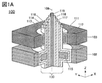
- FIG. 1A is a perspective view of a memory cell.
- FIG. 1B is a cross-sectional view of the memory cell.
- 2A and 2B are cross-sectional views of the memory cell.
- FIG. 3 is a perspective view of the structure.
- 4A to 4C are equivalent circuit diagrams of memory cells.
- 5A and 5B are equivalent circuit diagrams of memory cells.
- FIG. 6 is a cross-sectional view of the memory string.
- FIG. 7 is an equivalent circuit diagram of the memory string.
- FIG. 8 is an equivalent circuit diagram of the memory string.
- FIG. 9 is an equivalent circuit diagram of the memory string.
- FIG. 10 is an equivalent circuit diagram of a memory string.
- 11A and 11B are top views of the memory string.
- 12A and 12B are cross-sectional views of the memory cell.
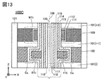
- FIG. 13 is a cross-sectional view of the memory cell.
- FIG. 14A is a diagram illustrating the classification of crystal structures.
- FIG. 14B is a diagram illustrating an XRD spectrum of the CAAC-IGZO film.
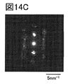
- FIG. 14C is a diagram illustrating a microelectron diffraction pattern of the CAAC-IGZO film.
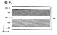
- 15A and 15B are cross-sectional views illustrating a method of manufacturing a memory cell.
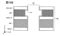
- 16A and 16B are cross-sectional views illustrating a method of manufacturing a memory cell.
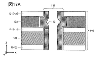
- 17A and 17B are cross-sectional views illustrating a method of manufacturing a memory cell.
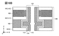
- 18A and 18B are cross-sectional views illustrating a method of manufacturing a memory cell.
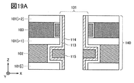
- 19A and 19B are cross-sectional views illustrating a method of manufacturing a memory cell.
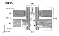
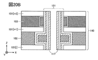
- 20A and 20B are cross-sectional views illustrating a method of manufacturing a memory cell.
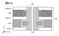
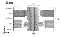
- 21A and 21B are cross-sectional views illustrating a method of manufacturing a memory cell.
- 22A and 22B are cross-sectional views illustrating a method of manufacturing a memory cell.
- FIG. 23 is a circuit diagram of the semiconductor device.
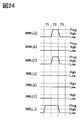
- FIG. 24 is a timing chart illustrating an operation example of the semiconductor device.
- 25A and 25B are timing charts for explaining an operation example of the semiconductor device.
- FIG. 26A is a perspective view illustrating a configuration example of the semiconductor device.
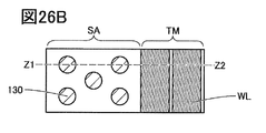
- FIG. 26B is a top view illustrating a configuration example of the semiconductor device.
- FIG. 26C is a cross-sectional view illustrating a configuration example of the semiconductor device.
- FIG. 27A is a perspective view illustrating a configuration example of the semiconductor device.
- FIG. 27B is a top view illustrating a configuration example of the semiconductor device.
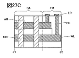
- FIG. 27C is a cross-sectional view illustrating a configuration example of the semiconductor device.
- 28A and 28B are cross-sectional views illustrating the semiconductor device.
- 29A and 29B are cross-sectional views illustrating the semiconductor device.
- FIG. 30 is a block diagram illustrating a configuration example of the semiconductor device.
- FIG. 31 is a diagram illustrating a configuration example of the semiconductor device.
- FIG. 32 is a diagram illustrating an example of constructing an information processing system using a plurality of storage devices.
- FIG. 33 is a block diagram illustrating a CPU.
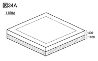
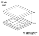
- 34A and 34B are perspective views of the semiconductor device.
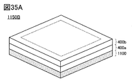
- 35A and 35B are perspective views of the semiconductor device.
- 36A and 36B are perspective views of the semiconductor device.
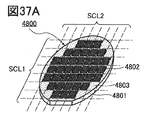
- 37A is a perspective view showing an example of a semiconductor wafer
- FIG. 37B is a perspective view showing an example of a chip
- FIGS. 37C and 37D are perspective views showing an example of an electronic component.
- 38A and 38B are diagrams showing various storage devices layer by layer.
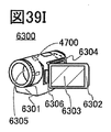
- 39A to 39J are perspective views or schematic views illustrating an example of an electronic device.
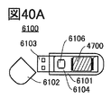
- 40A to 40E are perspective views or schematic views illustrating an example of an electronic device.
- 41A to 41C are diagrams illustrating an example of an electronic device.
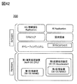
- FIG. 42 is a diagram illustrating a configuration example of a computer system.
- FIG. 43 is a diagram showing the hierarchical structure of the IoT network and the tendency of the required specifications.
- FIG. 44 is an image diagram of factory automation.
- FIG. 45A is a perspective conceptual diagram of the semiconductor device.
- FIG. 45B is an equivalent circuit diagram of a memory cell.
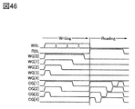
- FIG. 46 is a timing chart illustrating the operation of the 3DOSN AND string.
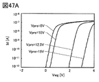
- FIG. 47A is a diagram showing the Id-Vwg characteristics of the transistor WTr.
- FIG. 47B is a diagram showing the relationship between the threshold voltage of the transistor WTr and Vpre.
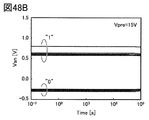
- 48A and 48B are diagrams showing the holding characteristics of the 3DOS NAND string.
- 49A and 49B are diagrams showing simulation results of memory cell holding characteristics.
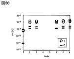
- FIG. 50 is a diagram showing simulation results of memory cell holding data and read current Irbl.
- the semiconductor device is a device utilizing semiconductor characteristics, and refers to a circuit including a semiconductor element (transistor, diode, photodiode, etc.), a device having the same circuit, and the like. It also refers to all devices that can function by utilizing semiconductor characteristics. For example, an integrated circuit, a chip having an integrated circuit, and an electronic component in which the chip is housed in a package are examples of semiconductor devices. Further, the storage device, the display device, the light emitting device, the lighting device, the electronic device, and the like are themselves semiconductor devices, and may have the semiconductor device.
- an element for example, a switch, a transistor, a capacitive element, an inductor, a resistance element, a diode, a display
- One or more devices, light emitting devices, loads, etc. can be connected between X and Y.
- the switch has a function of controlling the on state and the off state. That is, the switch is in a conducting state (on state) or a non-conducting state (off state), and has a function of controlling whether or not a current flows.
- a circuit that enables functional connection between X and Y for example, a logic circuit (inverter, NAND circuit, NOR circuit, etc.), signal conversion, etc.) Circuits (digital-to-analog conversion circuit, analog-to-digital conversion circuit, gamma correction circuit, etc.), potential level conversion circuit (power supply circuit (boost circuit, step-down circuit, etc.), level shifter circuit that changes the signal potential level, etc.), voltage source, current source , Switching circuit, amplification circuit (circuit that can increase signal amplitude or current amount, operational amplifier, differential amplification circuit, source follower circuit, buffer circuit, etc.), signal generation circuit, storage circuit, control circuit, etc.) It is possible to connect one or more to and from. As an example, even if another circuit is sandwiched between X and Y, if the signal output from X is transmitted to Y, it is assumed that X and Y are functionally connected. To do.
- X and Y are electrically connected, it means that X and Y are electrically connected (that is, another element between X and Y). Or when they are connected with another circuit in between) and when X and Y are directly connected (that is, they are connected without another element or another circuit between X and Y). If there is) and.
- X and Y, the source (or the first terminal, etc.) and the drain (or the second terminal, etc.) of the transistor are electrically connected to each other, and the X, the source (or the second terminal, etc.) of the transistor are connected to each other. (1 terminal, etc.), the drain of the transistor (or the 2nd terminal, etc.), and Y are electrically connected in this order.
- the source of the transistor (or the first terminal, etc.) is electrically connected to X
- the drain of the transistor (or the second terminal, etc.) is electrically connected to Y
- the X, the source of the transistor (such as the second terminal).
- the first terminal, etc.), the drain of the transistor (or the second terminal, etc.), and Y are electrically connected in this order.
- X is electrically connected to Y via the source (or first terminal, etc.) and drain (or second terminal, etc.) of the transistor, and X, the source (or first terminal, etc.) of the transistor. (Terminals, etc.), transistor drains (or second terminals, etc.), and Y are provided in this connection order.
- the source (or first terminal, etc.) and drain (or second terminal, etc.) of the transistor can be separated. Separately, the technical scope can be determined. Note that these expression methods are examples, and are not limited to these expression methods.
- X and Y are assumed to be objects (for example, devices, elements, circuits, wirings, electrodes, terminals, conductive films, layers, etc.).
- circuit diagram shows that the independent components are electrically connected to each other, one component has the functions of a plurality of components.
- one component has the functions of a plurality of components.
- the term "electrically connected” as used herein includes the case where one conductive film has the functions of a plurality of components in combination.
- the “resistance element” can be, for example, a circuit element having a resistance value higher than 0 ⁇ , wiring, or the like. Therefore, in the present specification and the like, the “resistive element” includes a wiring having a resistance value, a transistor in which a current flows between a source and a drain, a diode, a coil, and the like. Therefore, the term “resistance element” can be paraphrased into terms such as “resistance”, “load”, and “region having resistance value”, and conversely, the terms “resistance”, “load”, and “region having resistance value” are used. , “Resistance element” and so on.
- the resistance value can be, for example, preferably 1 m ⁇ or more and 10 ⁇ or less, more preferably 5 m ⁇ or more and 5 ⁇ or less, and further preferably 10 m ⁇ or more and 1 ⁇ or less. Further, for example, it may be 1 ⁇ or more and 1 ⁇ 10 9 ⁇ or less.
- the “capacitance element” means, for example, a circuit element having a capacitance value higher than 0F, a wiring region having a capacitance value, a parasitic capacitance, a transistor gate capacitance, and the like. Can be. Therefore, in the present specification and the like, the “capacitive element” is not only a circuit element containing a pair of electrodes and a dielectric contained between the electrodes, but also a parasitic element appearing between the wirings. It shall include the capacitance, the gate capacitance that appears between the gate and one of the source or drain of the transistor, and so on.
- capacitor element in addition, terms such as “capacitive element”, “parasitic capacitance”, and “gate capacitance” can be paraphrased into terms such as “capacity”, and conversely, the term “capacity” refers to “capacitive element”, “parasitic capacitance”, and “capacity”. It can be paraphrased into terms such as “gate capacitance”.
- the term “pair of electrodes” of “capacity” can be paraphrased as “pair of conductors", “pair of conductive regions", “pair of regions” and the like.
- the value of the capacitance can be, for example, 0.05 fF or more and 10 pF or less. Further, for example, it may be 1 pF or more and 10 ⁇ F or less.
- the transistor has three terminals called a gate, a source, and a drain.
- the gate is a control terminal that controls the conduction state of the transistor.
- the two terminals that function as sources or drains are the input and output terminals of the transistor.
- One of the two input / output terminals becomes a source and the other becomes a drain depending on the high and low potentials given to the conductive type (n-channel type, p-channel type) of the transistor and the three terminals of the transistor. Therefore, in the present specification and the like, the terms of source and drain can be paraphrased.
- the transistor when explaining the connection relationship of transistors, "one of the source or drain” (or the first electrode or the first terminal), “the other of the source or drain” (or the second electrode, or The notation (second terminal) is used.
- it may have a back gate in addition to the above-mentioned three terminals.
- one of the gate or the back gate of the transistor may be referred to as a first gate
- the other of the gate or the back gate of the transistor may be referred to as a second gate.
- the terms “gate” and “backgate” may be interchangeable.
- the respective gates When the transistor has three or more gates, the respective gates may be referred to as a first gate, a second gate, a third gate, and the like in the present specification and the like.
- a node can be paraphrased as a terminal, a wiring, an electrode, a conductive layer, a conductor, an impurity region, or the like, depending on a circuit configuration, a device structure, or the like.
- terminals, wiring, etc. can be paraphrased as nodes.
- ground potential ground potential
- the potentials are relative, and when the reference potential changes, the potential given to the wiring, the potential applied to the circuit or the like, the potential output from the circuit or the like also changes.
- high level potential also referred to as” high level potential ",” H potential “, or” H
- low level potential low level potential
- L low level potential
- the "current” is a charge transfer phenomenon (electrical conduction).
- the description “electrical conduction of a positively charged body is occurring” means “electrical conduction of a negatively charged body in the opposite direction”. Is happening. " Therefore, in the present specification and the like, “current” refers to a charge transfer phenomenon (electrical conduction) accompanying the movement of carriers, unless otherwise specified.
- the carriers referred to here include electrons, holes, anions, cations, complex ions, etc., and the carriers differ depending on the system in which the current flows (for example, semiconductor, metal, electrolyte, vacuum, etc.).
- the "current direction” in the wiring or the like is the direction in which the positive carrier moves, and the amount of current is described as a positive value.
- the direction in which the negative carrier moves is opposite to the direction of the current, and the amount of current is described as a negative value. Therefore, in the present specification and the like, if there is no notice about the positive or negative of the current (or the direction of the current), the description such as “current flows from element A to element B” means “current flows from element B to element A” or the like. It can be paraphrased as. Further, the description such as “a current is input to the element A” can be rephrased as "a current is output from the element A” or the like.
- the ordinal numbers “first”, “second”, and “third” are added to avoid confusion of the components. Therefore, the number of components is not limited. Moreover, the order of the components is not limited. For example, the component referred to in “first” in one of the embodiments of the present specification and the like may be the component referred to in “second” in another embodiment or in the claims. There can also be. Further, for example, the component mentioned in “first” in one of the embodiments of the present specification and the like may be omitted in another embodiment or in the claims.
- the terms “upper” and “lower” do not limit the positional relationship of the components to be directly above or directly below and to be in direct contact with each other.
- the terms “electrode B on the insulating layer A” it is not necessary that the electrode B is formed in direct contact with the insulating layer A, and another configuration is formed between the insulating layer A and the electrode B. Do not exclude those that contain elements.
- the positional relationship of the constituent elements changes as appropriate according to the direction in which each configuration is depicted. Therefore, it is not limited to the words and phrases explained in the specification and the like, and can be appropriately paraphrased according to the situation.
- terms indicating the arrangement such as “above” and “below” may be used for convenience in order to explain the positional relationship of the components with reference to the drawings. Therefore, in the expression of "insulator located on the upper surface of the conductor”, it can be rephrased as “insulator located on the lower surface of the conductor” by rotating the direction of the drawing shown by 180 degrees. Further, in the expression of "insulator located on the upper surface of the conductor”, it can be paraphrased as "insulator located on the left side (or right side) of the conductor” by rotating the direction of the drawing shown by 90 degrees. it can.
- electrode B overlapping the insulating layer A is not limited to the state of "the electrode B is formed on the insulating layer A", but “the electrode B is formed under the insulating layer A”. It does not exclude the state of "being” or the state of "the electrode B is formed on the right side (or left side) of the insulating layer A”.
- the terms “adjacent” and “proximity” do not limit that the components are in direct contact with each other.
- electrode B adjacent to the insulating layer A it is not necessary that the insulating layer A and the electrode B are formed in direct contact with each other, and another component is formed between the insulating layer A and the electrode B. Do not exclude those that include.
- membrane and layer can be interchanged with each other depending on the situation.
- Electrode may be used as part of a “wiring” and vice versa.
- the terms “electrode” and “wiring” include the case where a plurality of “electrodes” and “wiring” are integrally formed.
- a “terminal” may be used as part of a “wiring” or “electrode” and vice versa.
- the term “terminal” includes a case where a plurality of "electrodes", “wiring”, “terminals” and the like are integrally formed.
- the "electrode” can be a part of the “wiring” or the “terminal”, and for example, the “terminal” can be a part of the “wiring” or the “electrode”.
- terms such as “electrode”, “wiring”, and “terminal” may be replaced with terms such as "area” in some cases.
- terms such as “wiring”, “signal line”, and “power supply line” can be interchanged with each other in some cases or depending on the situation.
- the reverse is also true, and it may be possible to change terms such as “signal line” and “power supply line” to the term “wiring”.
- a term such as “power line” may be changed to a term such as "signal line”.
- terms such as “signal line” may be changed to terms such as "power line”.
- the term “potential” applied to the wiring may be changed to a term such as “signal” in some cases or depending on the situation.
- the reverse is also true, and terms such as “signal” may be changed to the term “potential”.
- the semiconductor impurities refer to, for example, other than the main components constituting the semiconductor layer.
- an element having a concentration of less than 0.1 atomic% is an impurity.
- the inclusion of impurities may result in, for example, an increase in the defect level density of the semiconductor, a decrease in carrier mobility, a decrease in crystallinity, and the like.
- the impurities that change the characteristics of the semiconductor include, for example, group 1 element, group 2 element, group 13 element, group 14 element, group 15 element, and other than the main component.
- transition metals and the like and in particular, hydrogen (also contained in water), lithium, sodium, silicon, boron, phosphorus, carbon, nitrogen and the like.
- impurities that change the characteristics of the semiconductor include, for example, Group 1 elements other than oxygen and hydrogen, Group 2 elements, Group 13 elements, Group 15 elements, and the like. There is.
- the switch means a switch that is in a conductive state (on state) or a non-conducting state (off state) and has a function of controlling whether or not a current flows.
- the switch means a switch having a function of selecting and switching a path through which a current flows.
- an electric switch, a mechanical switch, or the like can be used. That is, the switch is not limited to a specific switch as long as it can control the current.
- Examples of electrical switches include transistors (for example, bipolar transistors, MOS transistors, etc.), diodes (for example, PN diodes, PIN diodes, Schottky diodes, MIM (Metal Insulator Metal) diodes, and MIS (Metal Insulator Semiconductor) diodes. , Diode-connected transistors, etc.), or logic circuits that combine these.
- transistors for example, bipolar transistors, MOS transistors, etc.
- diodes for example, PN diodes, PIN diodes, Schottky diodes, MIM (Metal Insulator Metal) diodes, and MIS (Metal Insulator Semiconductor) diodes. , Diode-connected transistors, etc.
- the "conducting state" of the transistor means a state in which the source electrode and the drain electrode of the transistor can be regarded as being electrically short-circuited.
- the "non-conducting state" of the transistor means a state in which the source electrode and the drain electrode of the transistor can be regarded as being electrically cut off.
- the polarity (conductive type) of the transistor is not particularly limited.
- a mechanical switch is a switch using MEMS (Micro Electro Mechanical System) technology.
- the switch has an electrode that can be moved mechanically, and by moving the electrode, it operates by controlling conduction and non-conduction.
- the “on current” may mean a current flowing between the source and the drain when the transistor is in the on state.
- the “off current” may mean a current flowing between the source and the drain when the transistor is in the off state.
- parallel means a state in which two straight lines are arranged at an angle of ⁇ 10 ° or more and 10 ° or less. Therefore, the case of ⁇ 5 ° or more and 5 ° or less is also included.
- substantially parallel or approximately parallel means a state in which two straight lines are arranged at an angle of ⁇ 30 ° or more and 30 ° or less.
- vertical means a state in which two straight lines are arranged at an angle of 80 ° or more and 100 ° or less. Therefore, the case of 85 ° or more and 95 ° or less is also included.
- substantially vertical or “approximately vertical” means a state in which two straight lines are arranged at an angle of 60 ° or more and 120 ° or less.
- a metal oxide is a metal oxide in a broad sense. Metal oxides are classified into oxide insulators, oxide conductors (including transparent oxide conductors), oxide semiconductors (also referred to as Oxide Semiconductor or simply OS) and the like. For example, when a metal oxide is used in the active layer of a transistor, the metal oxide may be referred to as an oxide semiconductor. That is, when a metal oxide can form a channel forming region of a transistor having at least one of an amplification action, a rectifying action, and a switching action, the metal oxide is referred to as a metal oxide semiconductor. be able to. Further, when describing as an OS transistor, it can be paraphrased as a transistor having a metal oxide or an oxide semiconductor.
- a metal oxide having nitrogen may also be collectively referred to as a metal oxide. Further, a metal oxide having nitrogen may be referred to as a metal oxynitride.
- the configuration shown in each embodiment can be appropriately combined with the configuration shown in other embodiments to form one aspect of the present invention. Further, when a plurality of configuration examples are shown in one embodiment, the configuration examples can be appropriately combined with each other.
- the content (may be a part of the content) described in one embodiment is the other content (may be a part of the content) described in the embodiment and one or more other implementations. It is possible to apply, combine, or replace at least one content with the content described in the form of (may be a part of the content).
- figure (which may be a part) described in one embodiment is different from another part of the figure, another figure (which may be a part) described in the embodiment, and one or more other figures.
- the figure (which may be a part) described in the embodiment is different from another part of the figure, another figure (which may be a part) described in the embodiment, and one or more other figures.
- more figures can be formed.
- the size, layer thickness, or area may be exaggerated for clarity. Therefore, it is not necessarily limited to its size and aspect ratio.
- the drawings schematically show ideal examples, and are not limited to the shapes or values shown in the drawings. For example, it is possible to include variations in the signal, voltage, or current due to noise, or variations in the signal, voltage, or current due to timing lag.
- the code is used for identification such as "_1", “[n]", “[m, n]”. May be added and described.
- one of the two wiring GLs may be described as wiring GL [1], and the other may be described as wiring GL [2].
- FIG. 1A shows a perspective view of the memory cell 100 according to one aspect of the present invention.
- the memory cell 100 is a storage device having a three-dimensional laminated structure.
- a part of the memory cell 100 is omitted in order to show the internal structure of the memory cell 100.
- arrows indicating the X direction, the Y direction, and the Z direction may be added.
- the X, Y, and Z directions are directions that are orthogonal to each other. In the present specification and the like, one of the X direction, the Y direction, and the Z direction may be referred to as a "first direction" or a "first direction".
- the other one may be referred to as a "second direction” or a "second direction”. Further, the remaining one may be referred to as a "third direction” or a “third direction”. In the present embodiment and the like, the direction in which the structure 130, which will be described later, extends is the Z direction.
- FIG. 1B is a cross-sectional view showing a part of the memory cell 100 shown in FIG. 1A. Further, FIG. 1B is a cross-sectional view of a part of the memory cell 100 as viewed from the Y direction. Further, FIG. 1B is a cross-sectional view of an XZ plane passing through the central axis 108.
- FIG. 2A is a cross-sectional view of the portions A1-A2 shown by the alternate long and short dash line in FIG. 1B as viewed from the Z direction.
- FIG. 2B is a cross-sectional view of the portions B1-B2 shown by the alternate long and short dash line in FIG. 1B as viewed from the Z direction.
- the memory cell 100 has a plurality of insulators 101 arranged above the substrate (not shown).
- the plurality of insulators 101 are laminated in order from the substrate side.
- the i-th insulator 101 (i is an integer of 1 or more) is referred to as an insulator 101 [i].
- FIG. 1B shows an insulator 101 [i + 1] arranged above the insulator 101 [i] and an insulator 101 [i + 2] arranged above the insulator 101 [i + 1].
- the conductor 102 is provided between the insulator 101 [i] and the insulator 101 [i + 1]
- the conductor 103 is provided between the insulator 101 [i + 1] and the insulator 101 [i + 2].
- the insulator 101, the conductor 102, and the conductor 103 extend along the Y direction. Further, the memory cell 100 has an insulator 121 so as to cover the side surfaces of the insulator 101, the conductor 102, and the conductor 103.
- the memory cell 100 has a structure 130.
- the structure 130 extends in the Z direction along the central axis 108.
- FIG. 3 shows a perspective view of the structure 130.
- the structure 130 has a columnar shape. In FIG. 3, a part of the structure 130 is omitted in order to show the internal structure of the structure 130. A part of the structure 130 functions as a part of the memory cell 100. Further, as shown in FIGS. 1 and 3, the structure 130 has irregularities on the side surfaces extending in the Z direction.
- the outer peripheral shape of the structure 130 is circular when the structure 130 is viewed from the Z direction is shown, but the outer peripheral shape of the structure 130 does not have to be circular.
- it may be a polygon such as a triangle or a quadrangle.
- the outer peripheral shape of the structure 130 may be formed of a curved line, or may be formed by combining a curved line and a straight line.
- the structure 130 has a region that intersects the conductor 102 (also referred to as “intersection R”) and a region that intersects the conductor 103 (also referred to as “intersection W”). Further, the structure 130 includes an insulator 111, a functional body 112, an insulator 113, a semiconductor 114, a conductor 115, an insulator 116, a semiconductor 117, an insulator 118, and a conductor 119.
- the conductor 119 extends in the Z direction along the central axis 108, and the insulator 118 is provided adjacent to the conductor 119. Further, the semiconductor 117 is provided adjacent to the insulator 118. Further, an insulator 116 is provided adjacent to the semiconductor 117.
- a semiconductor 114 is provided adjacent to the insulator 116, an insulator 113 is provided adjacent to the semiconductor 114, and a functional body 112 is provided adjacent to the insulator 113 at the intersection W.
- An insulator 111 is provided adjacent to the functional body 112.
- FIG. 2A is a cross-sectional view of the intersection W in the direction perpendicular to the Z direction. At the intersection W, the insulator 111, the functional body 112, the insulator 113, the semiconductor 114, the insulator 116, the semiconductor 117, and the insulator 118 are concentrically provided on the outside of the conductor 119.
- FIG. 2B is a cross-sectional view of the intersection R in the direction perpendicular to the Z direction.
- the insulator 113, the semiconductor 114, the conductor 115, the insulator 116, the semiconductor 117, and the insulator 118 are concentrically provided on the outside of the conductor 119.
- the transistor WTr is formed at the intersection W.
- the conductor 103 functions as a gate electrode of the transistor WTr. Therefore, the insulator 111, the functional body 112, and the insulator 113 function as the gate insulator of the transistor WTr.
- the semiconductor 114 functions as a semiconductor in which the channel of the transistor WTr is formed.
- FIG. 2A is also a cross-sectional view of the transistor WTr seen from the Z direction.
- the conductor 119, the insulator 118, the semiconductor 117, the insulator 116, and the conductor 115 function as the transistor RTr. Further, the conductor 115, the semiconductor 114, the insulator 113, and the conductor 102 function as capacitive elements Cs. Therefore, it can be said that the transistor RTr and the capacitive element Cs are formed at the intersection R.
- FIG. 2B is also a cross-sectional view of the transistor RTr as viewed from the Z direction.
- the functional body 112 included in the transistor WTr can function as a charge storage layer. By accumulating an electric charge in the functional body 112, the threshold voltage of the transistor WTr can be controlled. For example, by increasing the threshold voltage of the transistor WTr, the transistor WTr can be made into a normally-off type transistor.
- the charge can be injected into the functional body 112 from the conductor 103 via the insulator 111.
- the insulator 111 functions as an injection layer
- the insulator 113 functions as a block layer.
- the charge can be injected into the functional body 112 from the semiconductor 114 via the insulator 113.
- the insulator 113 functions as an injection layer
- the insulator 111 functions as a block layer.
- the thickness of the injection layer when viewed from the direction perpendicular to the Z direction is preferably thinner than that of the block layer.
- the transistor WTr can be called a MONOS (Metal Oxide Nitride Semiconductor) type transistor.
- MONOS Metal Organic Semiconductor
- n-type silicon or p-type silicon when n-type silicon or p-type silicon is used for the gate electrode, it can be called a SONOS (Silicon Oxide Nitride Semiconductor) type transistor.
- SONOS Silicon Oxide Nitride Semiconductor
- tantalum nitride when tantalum nitride is used for the gate electrode and aluminum oxide is used for the block layer, it can be called a TANOS (Tantalum nitride Oxide Nitride Semiconductor) type transistor.
- TANOS Tetantalum nitride Oxide Nitride Semiconductor
- tantalum nitride When tantalum nitride is used for the gate electrode and hafnium oxide is used for the block layer, it can be called a THNOS (Tantalum nitride Hafnium oxide Semiconductor) type transistor.
- THNOS Tetantalum nitride Hafnium oxide Semiconductor
- the functional body 112 that functions as the charge storage layer it is preferable to use a material having a bandgap smaller than that of the insulator 111 and the insulator 113.
- silicon oxide may be used for the insulator 111 and the insulator 113
- an insulator such as silicon nitride may be used for the functional body 112.
- silicon nitride it is preferable to use silicon-rich silicon nitride.
- silicon nitride when silicon nitride is used for the insulator 111 and the insulator 113, silicon nitride having a higher silicon content than the silicon nitride used for the insulator 111 and the insulator 113 may be used for the functional body 112.
- the functional body 112 that functions as the charge storage layer may be a semiconductor.
- a semiconductor such as silicon may be used as the functional body 112.
- a transistor WTr using a semiconductor for the functional body 112 can be called an FG (Floating Gate) type transistor.
- the insulator 111, the functional body 112, and the insulator 113 may each have a plurality of layers.
- the insulator that functions as a block layer may be a laminate of silicon oxide and aluminum oxide.
- FIG. 4A shows an equivalent circuit diagram of the memory cell 100.
- one of the source or drain of the transistor WTr is electrically connected to the semiconductor 114 and the other of the source or drain is electrically connected to the gate of the transistor RTr.
- the gate of the transistor WTr is electrically connected to the conductor 103.
- the transistor WTr is a transistor having a charge storage layer between the gate and the semiconductor layer.
- a part of the semiconductor 114 functions as a channel forming region of the transistor WTr.
- the other part of the semiconductor 114 also functions as a source or drain of the transistor WTr.
- the semiconductor 114 can also function as an electrode or wiring.
- a part of the conductor 103 functions as a gate of the transistor WTr.
- the transistor RTr shown in FIG. 4A is a transistor having a back gate.
- a part of the conductor 119 functions as a back gate of the transistor RTr.
- the other part of the semiconductor 114 and the conductor 115 function as a gate of the transistor RTr.
- a part of the conductor 102 functions as the other electrode of the capacitive element Cs.
- a part of the semiconductor 117 functions as one of the source and the drain of the transistor RTr.
- the other part of the semiconductor 117 also functions as the source or drain of the transistor RTr.
- the semiconductor 117 can also function as an electrode or wiring.
- FIG. 4B corresponds to an equivalent circuit diagram of the memory cells 100B and the memory cells 100C described later.
- a back gate may be provided in the transistor WTr.
- FIG. 4C shows a circuit configuration example in which the back gate of the transistor WTr is electrically connected to the conductor 119, a conductor electrically connected to the back gate of the transistor WTr may be provided in addition to the conductor 119. ..
- the circuit configuration may be as shown in FIG. 5A or FIG. 5B.
- the conductor 102 functions as one electrode of the capacitive element Cs.
- a part of the conductor 115 and the semiconductor 114 functions as the other electrode of the capacitive element Cs.
- a node at which the gate of the transistor RTr, the other of the source or drain of the transistor WTr, and the other electrode of the capacitive element Cs are electrically connected is referred to as a node ND.
- FIG. 6 shows a cross-sectional view of a memory string 200 including four memory cells 100 (memory cells 100 [1] to memory cells 100 [4]).
- the memory string 200 shown in FIG. 6 includes a nine-layer insulator 101 (insulator 101 [1] to insulator 101 [9]) and a four-layer conductor 102 (conductor 102 [1] to conductor 102 [9]. 4]) and a four-layer conductor 103 (conductor 103 [1] to conductor 103 [4]).
- FIG. 7 shows an equivalent circuit diagram of the memory string 200.
- the memory string 200 has a configuration in which four memory cells 100 are connected in series. Therefore, the memory string 200 is a NAND type storage device.
- OS may be added to the circuit symbol of the transistor in order to clearly indicate that the transistor is an OS transistor.
- Si a transistor using silicon in the semiconductor layer on which the channel is formed
- Si Si may be added to the circuit symbol of the transistor.
- FIG. 7 shows that the transistor WTr and the transistor RTr are OS transistors.
- the transistor WTr, the transistor RTr, and the capacitive element Cs included in the memory cell 100 [1] are shown as the transistor WTr [1], the transistor RTr [1], and the capacitive element Cs [1], respectively.
- the transistor WTr, the transistor RTr, and the capacitive element Cs included in the memory cells 100 [2] to the memory cells 100 [4] are also shown.
- the number of memory cells 100 included in the memory string 200 is not limited to 4. Assuming that the number of memory cells 100 included in the memory string 200 is n, n may be an integer of 2 or more.
- the drain (or source) of the transistor WTr [k] included in the memory cell 100 [k] (k is an integer of 1 or more and n or less) is used.
- the drain (or source) of the transistor RTr [k] included in the memory cell 100 [k] is electrically connected to the source (or drain) of the transistor WTr [k + 1] included in the memory cell 100 [k + 1]. It refers to a configuration electrically connected to the source (or drain) of the transistor RTr [k + 1] included in the memory cell 100 [k + 1].
- a single crystal semiconductor, a polycrystalline semiconductor, a microcrystal semiconductor, an amorphous semiconductor, or the like can be used alone or in combination.
- the semiconductor material for example, silicon, germanium, or the like can be used.
- compound semiconductors such as silicon germanium, silicon carbide, gallium arsenide, oxide semiconductors, and nitride semiconductors may be used.
- the semiconductor used for the transistor may be a laminate of semiconductors.
- semiconductors having different crystal states may be used, or different semiconductor materials may be used.
- both the semiconductor 114 and the semiconductor 117 may be oxide semiconductors. Further, both the semiconductor 114 and the semiconductor 117 may be silicon. Further, the semiconductor 114 may be an oxide semiconductor and the semiconductor 117 may be silicon. Further, the semiconductor 114 may be silicon and the semiconductor 117 may be an oxide semiconductor.
- the transistor WTr is preferably a transistor in which an oxide semiconductor, which is a kind of metal oxide, is used in the semiconductor layer on which a channel is formed. Since the oxide semiconductor has a band gap of 2 eV or more, the off-current is remarkably small.
- an OS transistor is used as the transistor WTr, the electric charge written in the node ND (also referred to as “storage node”) can be retained for a long period of time.
- the memory cell 100 can be referred to as an "OS memory”. Further, the memory string 200 including the memory cell 100 can also be called an “OS memory”.
- a NAND type storage device including an OS memory is also referred to as an "OS NAND type” or an “OS NAND type storage device”. Further, an OS NAND type storage device having a configuration in which a plurality of OS memories are stacked in the Z direction is also referred to as a "3D OS NAND type” or a “3D OS NAND type storage device”.
- the transistor RTr may be a transistor (also referred to as “Si transistor”) in which silicon is used in the semiconductor layer on which the channel is formed.
- the transistor RTr may be formed of a Si transistor, and the transistor WTr may be formed of an OS transistor.
- FIG. 8 shows an equivalent circuit diagram of the memory string 200 when an OS transistor is used as the transistor WTr and a Si transistor is used as the transistor RTr.
- the OS memory can retain the written information for a period of one year or more, or even ten years or more, even if the power supply is stopped. Therefore, the OS memory can be regarded as a non-volatile memory.
- the OS memory can hold not only binary information (1 bit) but also multi-value (multi-bit) information.
- the OS memory is a method of writing an electric charge to a node via an OS transistor, a high voltage required for a conventional flash memory is not required, and a high-speed writing operation can be realized. Further, the erasing operation before data rewriting performed in the flash memory is unnecessary in the OS memory. Also, since no charge is injected or withdrawn into the floating gate or charge capture layer, the OS memory can write and read data virtually unlimited times. The OS memory has less deterioration than the conventional flash memory, and high reliability can be obtained.
- OS memory does not undergo structural changes at the atomic level when data is rewritten. Therefore, the OS memory is superior in rewrite resistance to the magnetoresistive memory and the resistance change type memory.
- the off-current of the OS transistor hardly increases even in a high temperature environment. Specifically, the off-current hardly increases even at an environmental temperature of room temperature or higher and 200 ° C. or lower. In addition, the on-current does not easily decrease even in a high temperature environment.
- the storage device including the OS memory has stable operation even in a high temperature environment, and high reliability can be obtained. Further, the OS transistor has a high dielectric strength between the source and the drain. By using an OS transistor as a transistor constituting a semiconductor device, operation is stable even in a high temperature environment, and a semiconductor device with good reliability can be realized.
- a Si transistor may be used as the transistor WTr and an OS transistor may be used as the transistor RTr depending on the purpose or application. Further, as shown in FIG. 10, a Si transistor may be used for both the transistor WTr and the transistor RTr depending on the purpose or application.
- the storage capacity per unit area can be increased.
- the plurality of memory cells 100 or the plurality of memory strings 200 are arranged in a staggered grid pattern (see FIG. 11A) or in a grid pattern (FIG. 11A). 11B) may be provided.
- FIG. 11 is a top view of the memory string.
- Table 1 shows a comparison table of a 3D NAND type storage device made of a Si transistor and a 3D OS NAND type storage device.
- FIG. 12A shows a cross-sectional view of the memory cell 100A.
- the memory cell 100A is a modification of the memory cell 100. Therefore, in the present embodiment and the like, the points different from the memory cell 100 of the memory cell 100A will be mainly described.
- a semiconductor 114 is provided adjacent to the insulator 116 and a conductor 115 is provided adjacent to the semiconductor 114 at the intersection R.
- the insulator 113 may be provided adjacent to the conductor 115.
- the conductor 119, the insulator 118, the semiconductor 117, the insulator 116, the semiconductor 114, and the conductor 115 function as the transistor RTr.
- the semiconductor 114 may function as a gate electrode. Further, the semiconductor 114 may function as a gate insulator. Further, the conductor 115, the insulator 113, and the conductor 102 function as capacitive elements Cs.
- FIG. 12B shows a cross-sectional view of the memory cell 100B.
- the memory cell 100B is a modification of the memory cell 100.
- the formation of the conductor 119 that functions as a back gate may be omitted, and the conductor 118 may be filled.
- the manufacturing process can be simplified and the productivity of the storage device can be increased.
- FIG. 13 shows a cross-sectional view of the memory cell 100C.
- the memory cell 100C is a modification of the memory cell 100, and is also a modification of the memory cell 100B.
- the formation of the conductor 119 that functions as a back gate may be omitted, and the cavity 120 may be formed without filling the area where the conductor 119 is to be formed.
- the memory cell 100 and the memory string 200 can be provided on the substrate.
- the substrate for example, an insulator substrate, a semiconductor substrate, or a conductor substrate may be used.
- the insulator substrate include a glass substrate, a quartz substrate, a sapphire substrate, a stabilized zirconia substrate (yttria-stabilized zirconia substrate, etc.), a resin substrate, and the like.
- the semiconductor substrate includes, for example, a semiconductor substrate made of silicon or germanium, or a compound semiconductor made of silicon carbide, silicon germanium, gallium arsenide, indium phosphide, zinc oxide, gallium oxide, gallium nitride (GaN), or the like. There is a board.
- the conductor substrate includes a graphite substrate, a metal substrate, an alloy substrate, and a conductive resin substrate.
- a substrate having a metal nitride a substrate having a metal oxide, and the like.
- a substrate in which a conductor or a semiconductor is provided in an insulator substrate a substrate in which a conductor or an insulator is provided in a semiconductor substrate, a substrate in which a semiconductor or an insulator is provided in a conductor substrate, and the like.
- those on which an element is provided may be used.
- Elements provided on the substrate include a capacitance element, a resistance element, a switch element, a light emitting element, a storage element, and the like.
- Insulator examples include oxides, nitrides, oxide nitrides, nitride oxides, metal oxides, metal oxide nitrides, metal nitride oxides and the like having insulating properties.
- the material may be selected according to the function of the insulator.
- Examples of the insulator having a high specific dielectric constant include gallium oxide, hafnium oxide, zirconium oxide, oxides having aluminum and hafnium, nitrides having aluminum and hafnium, oxides having silicon and hafnium, silicon and hafnium. There are nitrides having oxides, or nitrides having silicon and hafnium.
- Examples of insulators having a low specific dielectric constant include silicon oxide, silicon oxide, silicon nitride, silicon nitride, silicon oxide added with fluorine, silicon oxide added with carbon, silicon oxide added with carbon and nitrogen, and empty. There are silicon oxide having holes, resin, and the like.
- the OS transistor can stabilize the electrical characteristics of the transistor by surrounding it with an insulator having a function of suppressing the permeation of impurities such as hydrogen and oxygen.
- the insulator having a function of suppressing the permeation of impurities such as hydrogen and oxygen include boron, carbon, nitrogen, oxygen, fluorine, magnesium, aluminum, silicon, phosphorus, chlorine, gallium, germanium, yttrium, zirconium, and lanthanum. Insulations containing, neodymium, hafnium, or tantalum may be used in single layers or in layers.
- an insulator having a function of suppressing the permeation of impurities such as hydrogen and oxygen
- Metal oxides such as tantalum oxide and metal nitrides such as aluminum nitride, silicon nitride and silicon nitride can be used.
- the “nitride oxide” refers to a material having a higher oxygen content than nitrogen as a main component.
- silicon oxide nitride refers to a material containing silicon, nitrogen, and oxygen, which has a higher oxygen content than nitrogen.
- the “nitride oxide” refers to a material having a higher nitrogen content than oxygen as a main component.
- aluminum nitride oxide refers to a material containing aluminum, nitrogen, and oxygen, which has a higher nitrogen content than oxygen.
- the insulator that functions as a gate insulator is preferably an insulator having a region containing oxygen that is desorbed by heating.
- the oxygen deficiency of the semiconductor 114 and / or the semiconductor 117 can be compensated. Can be done.
- the insulating layer formed of the above material may be used as a single layer as the insulator, but a plurality of insulating layers formed of the above material may be laminated and used.
- an insulator when an insulator is provided in contact with a conductor, it is preferable to use an insulator having a function of suppressing oxygen permeation as the insulator in order to prevent oxidation of the conductor.
- an insulator having a function of suppressing oxygen permeation for example, it is preferable to use hafnium oxide, aluminum oxide, silicon nitride or the like as the insulator.
- an insulator when an insulator is laminated adjacent to the conductor, it is preferable to use an insulator having a function of suppressing oxygen permeation as the insulator in contact with the conductor.
- hafnium oxide may be used to form an insulator in contact with a conductor
- silicon oxide may be used to form an insulator in contact with the insulator.
- Conductors include aluminum, chromium, copper, silver, gold, platinum, tantalum, nickel, titanium, molybdenum, tungsten, hafnium, vanadium, niobium, manganese, magnesium, zirconium, beryllium, indium, ruthenium, iridium, strontium, and lanthanum. It is preferable to use a metal element selected from the above, an alloy containing the above-mentioned metal element as a component, an alloy in which the above-mentioned metal element is combined, or the like.
- tantalum nitride, titanium nitride, tungsten, nitrides containing titanium and aluminum, nitrides containing tantalum and aluminum, ruthenium oxide, ruthenium nitride, oxides containing strontium and ruthenium, oxides containing lanthanum and nickel, etc. are used. Is preferable.
- tantalum nitride, titanium nitride, nitrides containing titanium and aluminum, nitrides containing tantalum and aluminum, ruthenium oxide, ruthenium nitride, oxides containing strontium and ruthenium, and oxides containing lanthanum and nickel are difficult to oxidize.
- the conductive layer formed of the above material may be used as a single layer, but a plurality of conductive layers formed of the above material may be laminated and used.
- a laminated structure may be formed in which the above-mentioned material containing a metal element and a conductive material containing oxygen are combined.
- a laminated structure may be formed in which the above-mentioned material containing a metal element and a conductive material containing nitrogen are combined.
- a laminated structure may be formed in which the above-mentioned material containing a metal element, a conductive material containing oxygen, and a conductive material containing nitrogen are combined.
- the conductor functioning as the gate electrode includes the above-mentioned material containing a metal element, a conductive material containing oxygen, and the like. It is preferable to use a laminated structure in which the above is combined. In this case, a conductive material containing oxygen may be provided on the channel forming region side. By providing the conductive material containing oxygen on the channel forming region side, oxygen separated from the conductive material can be easily supplied to the channel forming region.
- a conductor that functions as a gate electrode it is preferable to use a conductive material containing a metal element contained in an oxide semiconductor in which a channel is formed and oxygen.
- the above-mentioned conductive material containing a metal element and nitrogen may be used.
- a conductive material containing nitrogen such as titanium nitride and tantalum nitride may be used.
- indium tin oxide, indium oxide containing tungsten oxide, indium zinc oxide containing tungsten oxide, indium oxide containing titanium oxide, indium tin oxide containing titanium oxide, indium zinc oxide, and silicon were added.
- Indium tin oxide may be used.
- indium gallium zinc oxide containing nitrogen may be used.
- Oxide semiconductor As the semiconductor 114 and / or the semiconductor 117, it is preferable to use a metal oxide (oxide semiconductor) that functions as a semiconductor. In particular, it is preferable to use an oxide semiconductor for the semiconductor 114.
- oxide semiconductor for the semiconductor 114.
- the oxide semiconductor applicable to the memory cell 100 will be described.
- the oxide semiconductor preferably contains at least indium or zinc. In particular, it preferably contains indium and zinc. In addition to them, it is preferable that aluminum, gallium, yttrium, tin and the like are contained. Further, one or more selected from boron, titanium, iron, nickel, germanium, zirconium, molybdenum, lanthanum, cerium, neodymium, hafnium, tantalum, tungsten, magnesium, cobalt and the like may be contained.
- the oxide semiconductor is an In—M—Zn oxide having indium, the element M, and zinc.
- the element M may be one or more selected from aluminum, gallium, yttrium, and tin.
- Other elements applicable to the element M include boron, titanium, iron, nickel, germanium, zirconium, molybdenum, lanthanum, cerium, neodymium, hafnium, tantalum, tungsten, magnesium, cobalt and the like.
- the element M a plurality of the above-mentioned elements may be combined in some cases.
- FIG. 14A is a diagram illustrating classification of crystal structures of oxide semiconductors, typically IGZO (metal oxides containing In, Ga, and Zn).
- IGZO metal oxides containing In, Ga, and Zn
- oxide semiconductors are roughly classified into “Amorphous”, “Crystalline”, and “Crystal”.
- Amorphous includes complete amorphous.
- Crystalline includes CAAC (c-axis-aligned crystalline), nc (nanocrystalline), and CAC (cloud-aligned composite).
- single crystal, poly crystal, and single crystal amorphous are excluded from the classification of "Crystalline”.
- “Crystal” includes single crystal and poly crystal.
- the structure in the thick frame shown in FIG. 14A is an intermediate state between "Amorphous” and “Crystal", and belongs to a new boundary region (New crystal line phase). .. That is, the structure can be rephrased as a structure completely different from the energetically unstable "Amorphous” and "Crystal".
- the crystal structure of the film or substrate can be evaluated using an X-ray diffraction (XRD: X-Ray Diffraction) spectrum.
- XRD X-ray diffraction
- FIG. 14B the XRD spectrum obtained by GIXD (Glazing-Incidence XRD) measurement of a CAAC-IGZO film classified as "Crystalline" is shown in FIG. 14B.
- the GIXD method is also referred to as a thin film method or a Seemann-Bohlin method.
- the XRD spectrum obtained by the GIXD measurement shown in FIG. 14B will be simply referred to as an XRD spectrum.
- the thickness of the CAAC-IGZO film shown in FIG. 14B is 500 nm.
- a peak showing clear crystallinity is detected in the XRD spectrum of the CAAC-IGZO film.
- the crystal structure of the film or substrate can be evaluated by a diffraction pattern (also referred to as a microelectron diffraction pattern) observed by a micro electron diffraction method (NBED: Nano Beam Electron Diffraction).
- the diffraction pattern of the CAAC-IGZO film is shown in FIG. 14C.
- FIG. 14C is a diffraction pattern observed by the NBED in which the electron beam is incident parallel to the substrate.
- electron diffraction is performed with the probe diameter set to 1 nm.
- oxide semiconductors When focusing on the crystal structure, oxide semiconductors may be classified differently from FIG. 14A.
- oxide semiconductors are divided into single crystal oxide semiconductors and other non-single crystal oxide semiconductors.
- the non-single crystal oxide semiconductor include CAAC-OS (C Axis Aligned Crystal Semiconductor) and nc-OS (nanocrystalline Oxide Semiconductor).
- the non-single crystal oxide semiconductor includes a polycrystalline oxide semiconductor, a pseudo-amorphous oxide semiconductor (a-like OS: amorphous-like oxide semiconductor), an amorphous oxide semiconductor, and the like.
- CAAC-OS is an oxide semiconductor having a plurality of crystal regions, and the plurality of crystal regions are oriented in a specific direction on the c-axis.
- the specific direction is the thickness direction of the CAAC-OS film, the normal direction of the surface to be formed of the CAAC-OS film, or the normal direction of the surface of the CAAC-OS film.
- the crystal region is a region having periodicity in the atomic arrangement. When the atomic arrangement is regarded as a lattice arrangement, the crystal region is also a region in which the lattice arrangement is aligned. Further, the CAAC-OS has a region in which a plurality of crystal regions are connected in the ab plane direction, and the region may have distortion.
- the strain refers to a region in which a plurality of crystal regions are connected in which the orientation of the lattice arrangement changes between a region in which the lattice arrangement is aligned and a region in which another grid arrangement is aligned. That is, CAAC-OS is an oxide semiconductor that is c-axis oriented and not clearly oriented in the ab plane direction.
- Each of the plurality of crystal regions is composed of one or a plurality of minute crystals (crystals having a maximum diameter of less than 10 nm).
- the maximum diameter of the crystal region is less than 10 nm.
- the size of the crystal region may be about several tens of nm.
- CAAC-OS contains a layer having indium (In) and oxygen (hereinafter, In layer) and a layer having elements M, zinc (Zn), and oxygen (hereinafter referred to as "In layer”). It tends to have a layered crystal structure (also referred to as a layered structure) in which (M, Zn) layers) are laminated. Indium and element M can be replaced with each other. Therefore, the (M, Zn) layer may contain indium. In addition, the In layer may contain the element M. The In layer may contain Zn.
- the layered structure is observed as a lattice image in, for example, a high-resolution TEM image.
- the position of the peak indicating the c-axis orientation may vary depending on the type and composition of the metal elements constituting CAAC-OS.
- a plurality of bright spots are observed in the electron diffraction pattern of the CAAC-OS film.
- a certain spot and another spot are observed at point-symmetrical positions with the spot of the incident electron beam passing through the sample (also referred to as a direct spot) as the center of symmetry.
- the lattice arrangement in the crystal region is based on a hexagonal lattice, but the unit lattice is not limited to a regular hexagon and may be a non-regular hexagon. Further, in the above strain, it may have a lattice arrangement such as a pentagon or a heptagon.
- a clear grain boundary cannot be confirmed even in the vicinity of strain. That is, it can be seen that the formation of grain boundaries is suppressed by the distortion of the lattice arrangement. This is because CAAC-OS can tolerate distortion because the arrangement of oxygen atoms is not dense in the ab plane direction and the bond distance between atoms changes due to the replacement of metal atoms. It is thought that this is the reason.
- CAAC-OS for which no clear crystal grain boundary is confirmed, is one of the crystalline oxides having a crystal structure suitable for the semiconductor layer of the transistor.
- a configuration having Zn is preferable.
- In-Zn oxide and In-Ga-Zn oxide are more suitable than In oxide because they can suppress the generation of grain boundaries.
- CAAC-OS is an oxide semiconductor having high crystallinity and no clear grain boundary is confirmed. Therefore, it can be said that CAAC-OS is unlikely to cause a decrease in electron mobility due to grain boundaries. Further, since the crystallinity of the oxide semiconductor may be lowered due to the mixing of impurities or the generation of defects, CAAC-OS can be said to be an oxide semiconductor having few impurities and defects (oxygen deficiency, etc.). Therefore, the oxide semiconductor having CAAC-OS has stable physical properties. Therefore, the oxide semiconductor having CAAC-OS is resistant to heat and has high reliability. CAAC-OS is also stable against high temperatures (so-called thermal budgets) in the manufacturing process. Therefore, when CAAC-OS is used for the OS transistor, the degree of freedom in the manufacturing process can be expanded.
- nc-OS has periodicity in the atomic arrangement in a minute region (for example, a region of 1 nm or more and 10 nm or less, particularly a region of 1 nm or more and 3 nm or less).
- nc-OS has tiny crystals. Since the size of the minute crystal is, for example, 1 nm or more and 10 nm or less, particularly 1 nm or more and 3 nm or less, the minute crystal is also referred to as a nanocrystal.
- nc-OS does not show regularity in crystal orientation between different nanocrystals. Therefore, no orientation is observed in the entire film.
- the nc-OS may be indistinguishable from the a-like OS and the amorphous oxide semiconductor depending on the analysis method. For example, when a structural analysis is performed on an nc-OS film using an XRD apparatus, a peak indicating crystallinity is not detected in the Out-of-plane XRD measurement using a ⁇ / 2 ⁇ scan. Further, when electron beam diffraction (also referred to as selected area electron diffraction) using an electron beam having a probe diameter larger than that of nanocrystals (for example, 50 nm or more) is performed on the nc-OS film, a diffraction pattern such as a halo pattern is performed. Is observed.
- electron beam diffraction also referred to as selected area electron diffraction
- nanocrystals for example, 50 nm or more
- electron diffraction also referred to as nanobeam electron diffraction
- an electron beam having a probe diameter for example, 1 nm or more and 30 nm or less
- An electron diffraction pattern in which a plurality of spots are observed in a ring-shaped region centered on a direct spot may be acquired.
- the a-like OS is an oxide semiconductor having a structure between nc-OS and an amorphous oxide semiconductor.
- the a-like OS has a void or low density region. That is, a-like OS has lower crystallinity than nc-OS and CAAC-OS. In addition, a-like OS has a higher hydrogen concentration in the membrane than nc-OS and CAAC-OS.
- CAC-OS relates to the material composition.
- CAC-OS is, for example, a composition of a material in which the elements constituting the metal oxide are unevenly distributed in a size of 0.5 nm or more and 10 nm or less, preferably 1 nm or more and 3 nm or less, or a size close thereto.
- the metal oxide one or more metal elements are unevenly distributed, and the region having the metal element has a size of 0.5 nm or more and 10 nm or less, preferably 1 nm or more and 3 nm or less, or a size close thereto.
- the mixed state is also called a mosaic shape or a patch shape.
- CAC-OS has a structure in which the material is separated into a first region and a second region to form a mosaic shape, and the first region is distributed in the membrane (hereinafter, also referred to as a cloud shape). It says.). That is, CAC-OS is a composite metal oxide having a structure in which the first region and the second region are mixed.
- the atomic number ratios of In, Ga, and Zn with respect to the metal elements constituting CAC-OS in the In-Ga-Zn oxide are expressed as [In], [Ga], and [Zn], respectively.
- the first region is a region in which [In] is larger than [In] in the composition of the CAC-OS film.
- the second region is a region in which [Ga] is larger than [Ga] in the composition of the CAC-OS film.
- the first region is a region in which [In] is larger than [In] in the second region and [Ga] is smaller than [Ga] in the second region.
- the second region is a region in which [Ga] is larger than [Ga] in the first region and [In] is smaller than [In] in the first region.
- the first region is a region in which indium oxide, indium zinc oxide, or the like is the main component.
- the second region is a region in which gallium oxide, gallium zinc oxide, or the like is the main component. That is, the first region can be rephrased as a region containing In as a main component. Further, the second region can be rephrased as a region containing Ga as a main component.
- a region containing In as a main component (No. 1) by EDX mapping acquired by using energy dispersive X-ray spectroscopy (EDX: Energy Dispersive X-ray spectroscopy). It can be confirmed that the region (1 region) and the region containing Ga as a main component (second region) have a structure in which they are unevenly distributed and mixed.
- EDX Energy Dispersive X-ray spectroscopy
- CAC-OS When CAC-OS is used for a transistor, the conductivity caused by the first region and the insulating property caused by the second region act in a complementary manner to switch the switching function (On / Off function). Can be added to the CAC-OS. That is, the CAC-OS has a conductive function in a part of the material and an insulating function in a part of the material, and has a function as a semiconductor in the whole material. By separating the conductive function and the insulating function, both functions can be maximized. Therefore, by using CAC-OS as a transistor, high on-current ( Ion ), high field-effect mobility ( ⁇ ), and good switching operation can be realized.
- Ion on-current
- ⁇ high field-effect mobility
- Oxide semiconductors have various structures, and each has different characteristics.
- the oxide semiconductor of one aspect of the present invention has two or more of amorphous oxide semiconductor, polycrystalline oxide semiconductor, a-like OS, CAC-OS, nc-OS, and CAAC-OS. You may.
- the oxide semiconductor as a transistor, a transistor having high field effect mobility can be realized. Moreover, a highly reliable transistor can be realized.
- the carrier concentration in the channel formation region of the oxide semiconductor is preferably 1 ⁇ 10 18 cm -3 or less, more preferably less than 1 ⁇ 10 17 cm -3 , and 1 ⁇ 10 16 cm -3. It is more preferably less than 1 ⁇ 10 13 cm -3 , even more preferably less than 1 ⁇ 10 12 cm -3.
- the impurity concentration in the oxide semiconductor film may be lowered to lower the defect level density.
- a low impurity concentration and a low defect level density is referred to as high-purity intrinsic or substantially high-purity intrinsic.
- An oxide semiconductor having a low carrier concentration may be referred to as a high-purity intrinsic or substantially high-purity intrinsic oxide semiconductor.
- high-purity intrinsic or substantially high-purity intrinsic may be referred to as i-type or substantially i-type.
- the trap level density may also be low.
- the charge captured at the trap level of the oxide semiconductor takes a long time to disappear, and may behave as if it were a fixed charge. Therefore, a transistor in which a channel formation region is formed in an oxide semiconductor having a high trap level density may have unstable electrical characteristics.
- Impurities include hydrogen, nitrogen, alkali metals, alkaline earth metals, iron, nickel, silicon and the like.
- the concentration of silicon and carbon in the channel formation region of the oxide semiconductor and the concentration of silicon and carbon near the interface with the channel formation region of the oxide semiconductor (secondary ion mass spectrometry (SIMS)). 2 ⁇ 10 18 atoms / cm 3 or less, preferably 2 ⁇ 10 17 atoms / cm 3 or less.
- the oxide semiconductor contains an alkali metal or an alkaline earth metal
- defect levels may be formed and carriers may be generated. Therefore, a transistor using an oxide semiconductor containing an alkali metal or an alkaline earth metal tends to have a normally-on characteristic. Therefore, the concentration of the alkali metal or alkaline earth metal in the channel formation region of the oxide semiconductor obtained by SIMS is set to 1 ⁇ 10 18 atoms / cm 3 or less, preferably 2 ⁇ 10 16 atoms / cm 3 or less. ..
- the nitrogen concentration in the channel formation region of the oxide semiconductor obtained by SIMS is less than 5 ⁇ 10 19 atoms / cm 3 , preferably 5 ⁇ 10 18 atoms / cm 3 or less, more preferably 1 ⁇ 10 18 atoms. / Cm 3 or less, more preferably 5 ⁇ 10 17 atoms / cm 3 or less.
- hydrogen contained in an oxide semiconductor reacts with oxygen bonded to a metal atom to become water, which may form an oxygen deficiency.
- oxygen deficiency When hydrogen enters the oxygen deficiency, electrons that are carriers may be generated.
- a part of hydrogen may be combined with oxygen that is bonded to a metal atom to generate an electron as a carrier. Therefore, a transistor using an oxide semiconductor containing hydrogen tends to have a normally-on characteristic. Therefore, it is preferable that hydrogen in the channel forming region of the oxide semiconductor is reduced as much as possible.
- the hydrogen concentration obtained by SIMS is less than 1 ⁇ 10 20 atoms / cm 3 , preferably less than 5 ⁇ 10 19 atoms / cm 3 , more preferably 1 ⁇ 10. It should be less than 19 atoms / cm 3 , more preferably less than 5 ⁇ 10 18 atoms / cm 3 , and even more preferably less than 1 ⁇ 10 18 atoms / cm 3 .
- the semiconductor material that can be used for the semiconductor 114 and the semiconductor 117 is not limited to the oxide semiconductor described above.
- a semiconductor material having a bandgap (a semiconductor material that is not a zero-gap semiconductor) may be used.
- a semiconductor of a single element such as silicon, a compound semiconductor such as gallium arsenide, a layered substance (also referred to as an atomic layer substance, a two-dimensional material, or the like) that functions as a semiconductor may be used as the semiconductor material.
- the layered substance is a general term for a group of materials having a layered crystal structure.
- a layered crystal structure is a structure in which layers formed by covalent bonds or ionic bonds are laminated via bonds weaker than covalent bonds or ionic bonds, such as van der Waals forces.
- the layered material has high electrical conductivity in the unit layer, that is, high two-dimensional electrical conductivity.
- Layered materials include graphene, silicene, chalcogenides and the like.
- Chalcogenides are compounds containing chalcogens.
- chalcogen is a general term for elements belonging to Group 16, and includes oxygen, sulfur, selenium, tellurium, polonium, and livermorium.
- Examples of chalcogenides include transition metal chalcogenides and group 13 chalcogenides.
- a transition metal chalcogenide that functions as a semiconductor may be used.
- molybdenum sulfide typically MoS 2
- molybdenum selenate typically MoSe 2
- molybdenum tellurium typically MoTe 2
- tungsten sulfide typically WS 2
- Tungsten selenate typically WSe 2
- tungsten tellurium typically WTe 2
- hafnium sulfide typically HfS 2
- hafnium selenate typically HfSe 2
- zirconium sulfide representative
- ZrS 2 zirconium selenium
- ZrSe 2 zirconium selenium
- the formation of conductors, insulators, and semiconductors is performed by a sputtering method, a CVD method, a molecular beam epitaxy (MBE) method, a pulsed laser deposition (PLD) method, or an atomic layer deposition (ALD) method. ) It can be done by using the method or the like.
- the CVD method can be classified into a plasma CVD (PECVD: Plasma Enhanced CVD) method using plasma, a thermal CVD (TCVD: Thermal CVD) method using heat, an optical CVD (Photo CVD) method using light, and the like. .. Further, it can be divided into a metal CVD (MCVD: Metal CVD) method and an organometallic CVD (MOCVD: Metal Organic CVD) method depending on the raw material gas used.
- PECVD Plasma Enhanced CVD
- TCVD Thermal CVD
- Photo CVD Photo CVD
- MCVD Metal CVD
- MOCVD Metal Organic CVD
- the plasma CVD method can obtain a high quality film at a relatively low temperature. Further, since the thermal CVD method does not use plasma, it is a film forming method capable of reducing plasma damage to the object to be processed. For example, wiring, electrodes, elements (transistors, capacitive elements, etc.) and the like included in a semiconductor device may be charged up by receiving electric charges from plasma. At this time, the accumulated electric charge may destroy the wiring, electrodes, elements, and the like included in the semiconductor device. On the other hand, in the case of the thermal CVD method that does not use plasma, such plasma damage does not occur, so that the yield of the semiconductor device can be increased. Further, in the thermal CVD method, plasma damage during film formation does not occur, so that a film having few defects can be obtained.
- the ALD method is also a film forming method capable of reducing plasma damage to the object to be processed. Further, the ALD method also does not cause plasma damage during film formation, so that a film having few defects can be obtained.
- the CVD method and the ALD method are different from the film forming method in which particles emitted from a target or the like are deposited, and are film forming methods in which a film is formed by a reaction on the surface of an object to be treated. Therefore, it is a film forming method that is not easily affected by the shape of the object to be treated and has good step coverage.
- the ALD method has excellent step covering property and excellent thickness uniformity, and is therefore suitable for covering the surface of an opening having a high aspect ratio.
- the ALD method since the ALD method has a relatively slow film forming rate, it may be preferable to use it in combination with another film forming method such as a CVD method having a high film forming rate.
- the composition of the obtained film can be controlled by the flow rate ratio of the raw material gas.
- a film having an arbitrary composition can be formed depending on the flow rate ratio of the raw material gas.
- a film having a continuously changed composition can be formed by changing the flow rate ratio of the raw material gas while forming the film.
- the inside of the chamber may be under atmospheric pressure or reduced pressure
- the raw material gas for the reaction is sequentially introduced into the chamber
- the film formation may be performed by repeating the order of introducing the gas.
- each switching valve also called a high-speed valve
- the first raw material gas is not mixed at the same time or after that so that the multiple kinds of raw materials gas are not mixed.
- An active gas argon, nitrogen, etc. or the like is introduced, and a second raw material gas is introduced.
- the inert gas becomes a carrier gas, and the inert gas may be introduced at the same time when the second raw material gas is introduced.
- the first raw material gas may be discharged by vacuum exhaust, and then the second raw material gas may be introduced.
- the first raw material gas is adsorbed on the surface of the substrate to form a first thin layer, and reacts with the second raw material gas introduced later, so that the second thin layer is on the first thin layer.
- a thin film is formed by being laminated on.
- Thermal CVD methods such as the MOCVD method and the ALD method can form various films such as a metal film, a semiconductor film, and an inorganic insulating film.
- a metal film such as a metal film, a semiconductor film, and an inorganic insulating film.
- an In-Ga-Zn-O film trimethylindium (In (CH 3 ) 3 ), trimethylgallium (Ga (CH 3 ) 3 ), and dimethylzinc (Zn (CH 3 ) 2) ) May be used.
- the combination is not limited to these, and triethylgallium (Ga (C 2 H 5 ) 3 ) can be used instead of trimethylgallium, and diethylzinc (Zn (C 2 H 5 ) 2 ) can be used instead of dimethylzinc.
- diethylzinc Zn (C 2 H 5 ) 2
- dimethylzinc can also be used.
- hafnium oxide film is formed by a film forming apparatus using ALD, a liquid containing a solvent and a hafnium precursor compound (hafnium alkoxide or tetrakisdimethylamide hafnium (TDHA, Hf [N (CH 3 ) 2 ]]. 4) a raw material gas hafnium amide) was vaporized, such as, using the two kinds of gases ozone (O 3) as an oxidizing agent.
- other materials include tetrakis (ethylmethylamide) hafnium and the like.
- a raw material gas obtained by vaporizing a liquid containing a solvent and an aluminum precursor compound (trimethylaluminum (TMA, Al (CH 3 ) 3), etc.).
- TMA trimethylaluminum
- Al Al (CH 3 ) 3
- H 2 O gases
- Other materials include tris (dimethylamide) aluminum, triisobutylaluminum, and aluminum tris (2,2,6,6-tetramethyl-3,5-heptane dinate).
- a silicon oxide film using a deposition apparatus employing ALD is hexachlorodisilane adsorbed on the film-forming surface, and supplying radicals for oxidizing gas (O 2, dinitrogen monoxide) adsorption React with things.
- oxidizing gas O 2, dinitrogen monoxide
- tungsten film when a tungsten film is formed by a film forming apparatus using ALD, WF 6 gas and B 2 H 6 gas are sequentially and repeatedly introduced to form an initial tungsten film, and then WF 6 gas and H 2 are formed. The gas is sequentially and repeatedly introduced to form a tungsten film.
- SiH 4 gas may be used instead of B 2 H 6 gas.
- an oxide semiconductor film for example, an In-Ga-Zn-O film is formed by a film forming apparatus using ALD
- In (CH 3 ) 3 gas and O 3 gas are sequentially and repeatedly introduced into In.
- the ⁇ O layer is formed, and then Ga (CH 3 ) 3 gas and O 3 gas are sequentially and repeatedly introduced to form a GaO layer, and then Zn (CH 3 ) 2 gas and O 3 gas are sequentially and repeatedly introduced.
- Zn (CH 3 ) 2 gas and O 3 gas are sequentially and repeatedly introduced.
- ZnO layer ZnO layer.
- these gases may be used to form a mixed oxide layer such as an In—Ga—O layer, an In—Zn—O layer, and a Ga—Zn—O layer.
- O 3 may be used of H 2 O gas obtained by bubbling water with an inert gas such as Ar in place of the gas, but better to use an O 3 gas containing no H are preferred.
- In (C 2 H 5 ) 3 gas may be used instead of In (CH 3 ) 3 gas.
- Ga (C 2 H 5 ) 3 gas may be used instead of Ga (CH 3 ) 3 gas.
- Zn (C 2 H 5 ) 2 gas may be used instead of Zn (CH 3 ) 2 gas.
- the laminate 140 shown in FIG. 15A is produced.
- the laminate 140 has an insulator 101, a conductor 102, and a conductor 103.
- the insulator 101 [i] is placed above the substrate (not shown), the conductor 102 is placed on the insulator 101 [i], the insulator 101 [i + 1] is placed on the conductor 102, and the conductor is conductive.
- the body 103 is arranged on the insulator 101 [i + 1], and the insulator 101 [i + 2] is arranged on the conductor 103.
- the insulator 101 is preferably a material having a reduced concentration of impurities such as water and hydrogen.
- the amount of desorption of hydrogen molecules of the insulator 101 per unit area is 2 ⁇ 10 15 in the range of 50 ° C. or higher and 500 ° C. or lower in the temperature desorption gas analysis method (TDS (Thermal Desorption Spectroscopy)).
- TDS Temperatur Desorption Gas analysis method
- the moles / cm 2 or less preferably 1 ⁇ 10 15 moles / cm 2 or less, more preferably 5 ⁇ 10 14 moles / cm 2 or less.
- an insulator in which oxygen is released by heating may be used as the insulator 101.
- the material applicable to the insulator 101 is not limited to the above description.
- the insulator 101 may have a laminated structure of a plurality of insulators.
- the insulator 101 may be a laminate of hafnium oxide and silicon oxide.
- a resist mask is formed on the laminate 140, and a part of the insulator 101, the conductor 103, and the conductor 102 is removed by an etching process using the resist mask as a mask, and an opening 131 is opened in the laminate 140. (See FIG. 15B).
- the resist mask can be formed by appropriately using, for example, a lithography method, a printing method, an inkjet method, or the like.
- the etching process may be a dry etching method or a wet etching method, or both may be used. Processing by the dry etching method is suitable for microfabrication.
- the resist mask In the formation of the resist mask by the lithography method, first, the resist is formed, and then the resist is exposed through the photomask. Next, the exposed region is removed or left with a developing solution to form a resist mask.
- a conductor, a semiconductor, an insulator, or the like can be processed into a desired shape.
- a resist mask may be formed by exposing the resist using KrF excimer laser light, ArF excimer laser light, EUV (Extreme Ultraviolet) light, or the like.
- an immersion technique may be used in which a liquid (for example, water) is filled between the substrate and the projection lens for exposure.
- an electron beam or an ion beam may be used instead of the above-mentioned light. When an electron beam or an ion beam is used, a photomask is not required.
- the resist mask can be removed by performing a dry etching process such as ashing, performing a wet etching process, performing a wet etching process after the dry etching process, or performing a dry etching process after the wet etching process.
- a dry etching process such as ashing, performing a wet etching process, performing a wet etching process after the dry etching process, or performing a dry etching process after the wet etching process.
- a hard mask made of an insulator or a conductor may be used instead of the resist mask.
- a hard mask an insulating film or a conductive film to be a hard mask material is formed on the conductive film, a resist mask is formed on the insulating film or a conductive film, and the hard mask material is etched to form a hard mask having a desired shape. be able to.
- a capacitively coupled plasma (CCP: Capacitively Coupled Plasma) etching apparatus having a parallel plate type electrode can be used as a dry etching apparatus for performing the etching process by the dry etching method.
- CCP Capacitively Coupled Plasma
- the capacitance coupling type plasma etching apparatus having the parallel plate type electrode may be configured to apply a high frequency power source to one electrode of the parallel plate type electrode.
- a plurality of different high-frequency power supplies may be applied to one of the parallel plate type electrodes.
- a high frequency power supply having the same frequency may be applied to each of the parallel plate type electrodes.
- a high frequency power supply having a different frequency may be applied to each of the parallel plate type electrodes.
- a dry etching apparatus having a high-density plasma source can be used.
- a dry etching apparatus having a high-density plasma source for example, an inductively coupled plasma (ICP: Inductively Coupled Plasma) etching apparatus or the like can be used.
- ICP Inductively Coupled Plasma
- a part of the conductor 103 exposed on the side surface of the opening 131 is etched to retract the conductor 103 from the side surface of the opening 131 (see FIG. 16A).
- the etching of the conductor 103 may be performed under conditions where a selection ratio with that of the insulator 101 and the conductor 102 can be obtained.
- the insulator 111 is formed along the side surface of the opening 131 (see FIG. 16B).
- the surfaces of the insulator 101, the conductor 103, and the conductor 102 exposed in the opening 131 are covered with the insulator 111.
- silicon oxide is used as the insulator 111.
- the insulator 111 may have a laminated structure of a plurality of insulators.
- the functional body 112 is formed along the surface of the insulator 111 (see FIG. 17A).
- silicon nitride is used as the insulator 111.
- the functional body 112 may have a laminated structure of a plurality of insulators.
- insulator 111 and the functional body 112 in the opening 131 is etched.
- the insulator 111 and the functional body 112 are etched except for the portion overlapping with the insulator 101 when viewed from the Z direction (see FIG. 17B).
- a part of the conductor 102 exposed on the side surface of the opening 131 is etched to retract the conductor 102 from the side surface of the opening 131 (see FIG. 18A).
- the etching of the conductor 102 may be performed under conditions where a selection ratio with that of the insulator 101 and the conductor 103 can be obtained.
- the insulator 113 is formed along the side surface of the opening 131 (see FIG. 18B).
- the surfaces of the insulator 101, the insulator 111, the functional body 112, and the conductor 102 exposed in the opening 131 are covered with the insulator 113.
- the semiconductor 114 When an oxide semiconductor is used for the semiconductor 114, for example, silicon oxide, silicon oxide nitride, or the like may be appropriately used as the insulator 113. By providing an insulator containing oxygen in contact with the semiconductor 114, oxygen deficiency in the semiconductor 114 can be reduced and the reliability of the transistor can be improved.
- silicon oxide, silicon oxide nitride, or the like may be appropriately used as the insulator 113.
- an oxide material in which a part of oxygen is desorbed by heating in other words, an insulator material having an excess oxygen region.
- An oxide that desorbs oxygen by heating has an oxygen molecule desorption amount of 1.0 ⁇ 10 18 molecules / cm 3 or more, preferably 1.0 ⁇ 10 19 molecules / cm 3 or more, as determined by TDS analysis. More preferably, it is an oxide film having 2.0 ⁇ 10 19 molecules / cm 3 or more, or 3.0 ⁇ 10 20 molecules / cm 3 or more.
- the surface temperature of the film during the TDS analysis is preferably in the range of 100 ° C. or higher and 700 ° C. or lower, or 100 ° C. or higher and 400 ° C. or lower.
- the insulator 113 may have a laminated structure of a plurality of insulators.
- an oxygenation treatment described later may be performed.
- the semiconductor 114 and the conductor 115 are formed along the side surface of the opening 131 (see FIG. 18B).
- the semiconductor 114 may have a laminated structure having a plurality of layers.
- the heat treatment may be performed, for example, at 100 ° C. or higher and 600 ° C. or lower, more preferably 350 ° C. or higher and 550 ° C. or lower.
- the heat treatment is performed in an atmosphere of nitrogen gas or an inert gas, or an atmosphere containing 10 ppm or more, 1% or more, or 10% or more of an oxidizing gas.
- the heat treatment is preferably performed in an oxygen atmosphere.
- oxygen can be supplied to the semiconductor 114 to reduce oxygen deficiency (VO ).
- the heat treatment may be performed in a reduced pressure state.
- the heat treatment may be performed in an atmosphere containing 10 ppm or more, 1% or more, or 10% or more of oxidizing gas in order to supplement the desorbed oxygen after heat treatment in an atmosphere of nitrogen gas or an inert gas.
- the heat treatment may be performed in an atmosphere containing 10 ppm or more, 1% or more, or 10% or more of the oxidizing gas, and then the heat treatment may be continuously performed in an atmosphere of nitrogen gas or an inert gas.
- the processing for supplying oxygen to the semiconductor 114 (also referred to as "oxygen supplying treatment”.) By performing the oxygen deficiency in the semiconductor 114, is repaired by supplied oxygen, when other words “V O + O ⁇ The reaction "null" can be promoted. Further, since the oxygen supplied to the hydrogen remaining in the semiconductor 114 reacts to remove the hydrogen as H 2 O (to dehydration) can. This allows the hydrogen which has been remaining in the semiconductor 114 can be inhibited from recombining to V O H is formed by oxygen vacancies.
- the oxygenation treatment can be performed by performing the microwave treatment in an atmosphere containing oxygen.
- the semiconductor 114 is irradiated with microwaves, high frequencies such as RF, oxygen plasma, oxygen radicals, and the like.
- microwave processing for example, it is preferable to use a microwave processing apparatus having a power source for generating high-density plasma using microwaves.
- the microwave processing apparatus may have a power source for applying RF to the substrate side.
- high-density plasma high-density oxygen radicals can be generated.
- RF radio frequency
- the microwave treatment is preferably performed under reduced pressure, and the pressure may be 60 Pa or more, preferably 133 Pa or more, more preferably 200 Pa or more, and further preferably 400 Pa or more.
- the oxygen flow rate ratio O 2 / (O 2 + Ar) is 50% or less, preferably 10% or more and 30% or less.
- the treatment temperature may be 750 ° C. or lower, preferably 500 ° C. or lower, for example, about 400 ° C.
- the heat treatment may be continuously performed without exposing to the outside air.
- Plasma by the action such as a microwave, and divide the V O H included in the semiconductor 114, it is possible to remove hydrogen H from the semiconductor 114. That is, in the semiconductor 114, it is possible to reduce the "V O H ⁇ H + V O ) ", happening further reaction of "V O + O ⁇ null", the hydrogen concentration of the semiconductor 114. Therefore, the oxygen deficiency in the semiconductor 114, and to reduce the V O H, the carrier concentration can be decreased.
- the conductor 115 is formed.
- tungsten is formed as the conductor 115.
- a part of the conductor 115 in the opening 131 is etched.
- the conductor 115 is etched except for the portion that overlaps with the semiconductor 114 when viewed from the Z direction (see FIG. 19A).
- the oxygenation treatment may be performed after the semiconductor 114 and the conductor 115 are exposed.
- the insulator 116 is formed along the side surface of the opening 131 (see FIG. 19B).
- the surfaces of the semiconductor 114 and the conductor 115 exposed in the opening 131 are covered with the insulator 116.
- an oxide semiconductor for the semiconductor 114, for example, silicon oxide, silicon oxide nitride, or the like may be appropriately used as the insulator 116.
- the insulator 116 the same material as the insulator 113 may be used.
- the insulator 116 may have a laminated structure of a plurality of insulators.
- the insulator 116 is preferably an insulator having a region containing oxygen desorbed by heating.
- the insulator 116 may have a laminated structure of a plurality of insulators.
- the insulator 116 may have a three-layer structure of silicon oxide or silicon oxide nitride, hafnium oxide or aluminum oxide, and silicon oxide or silicon oxide nitride. .. That is, a structure in which one layer of hafnium oxide or aluminum oxide is sandwiched between two layers of silicon oxide or silicon oxide may be used.
- the insulator 116 may have a laminated structure of two layers, or may have a laminated structure of four or more layers.
- An oxygenation treatment may be performed after the insulator 116 is formed (see FIG. 20A).
- the semiconductor 117 is formed along the side surface of the opening 131 (see FIG. 20B).
- the surface of the insulator 116 exposed in the opening 131 is covered with the semiconductor 117.
- oxygenation treatment may be performed in the same manner as when the oxide semiconductor is used for the semiconductor 114.
- the insulator 118 is formed along the side surface of the opening 131 (see FIG. 21A).
- the surface of the semiconductor 117 exposed in the opening 131 is covered with the insulator 118.
- an oxide semiconductor for the semiconductor 117
- silicon oxide, silicon oxide or the like may be appropriately used as the insulator 118.
- oxygen deficiency in the semiconductor 117 can be reduced and the reliability of the transistor can be improved.
- the insulator 118 the same material as the insulator 113 or the insulator 116 may be used.
- the insulator 118 may have a laminated structure of a plurality of insulators.
- the insulator in contact with the semiconductor 117 may be an insulator having a region containing oxygen desorbed by heating. preferable. Further, it is preferable to use an insulator having a function of suppressing oxygen permeation as the insulator in contact with the conductor 119.
- silicon oxide or silicon oxide nitride may be used as the insulator in contact with the semiconductor 117.
- hafnium oxide or aluminum oxide may be used as the insulator in contact with the conductor 119.
- the insulator 118 may be a laminate of silicon oxide or silicon nitride nitride, aluminum oxide, and silicon nitride.
- silicon nitride it is preferable to use silicon nitride having a low hydrogen content.
- the conductor 119 is formed after the insulator 118 is formed (see FIG. 21B).
- tungsten is used as the conductor 119.
- the conductor 119 may have a laminated structure of a plurality of conductors. Of the plurality of conductors constituting the conductor 119, it is preferable to use a conductive material that does not easily oxidize as the conductor in contact with the insulator 118.
- a conductive material that does not easily oxidize as the conductor in contact with the insulator 118.
- titanium nitride may be used as the conductor in contact with the insulator 118.
- the conductor 119 may be a laminate of titanium nitride and tungsten.
- the structure 130 is formed in the opening 131.
- a part of the laminated body 140 is removed in a region that does not overlap with the structure 130 when viewed from the Z direction to form a region 132 (see FIG. 22A).
- the region 132 can be formed in the same manner as the opening 131. In the region 132, the side surfaces of the insulator 101, the conductor 102, and the conductor 103 are exposed.
- the exposed insulator 101, the conductor 102, and the insulator 121 covering the side surfaces of the conductor 103 are formed (see FIG. 22B).
- the insulator 121 for example, it is preferable to use an insulating material having a function of suppressing permeation of impurities such as water and hydrogen.
- an insulating material having a function of suppressing permeation of impurities such as water and hydrogen.
- aluminum oxide or the like may be used as the insulator 121.
- the insulator 121 may have a laminated structure of a plurality of insulators.
- the insulator 121 may be a laminate of hafnium oxide and silicon oxide.
- the memory cell 100 can be manufactured.
- the circuit configuration of the semiconductor device 300 will be described with reference to FIG.
- the semiconductor device 300 has m memory strings 200.
- the first memory string 200 is referred to as a memory string 200 [1]
- the mth memory string 200 is referred to as a memory string 200 [m] (m is an integer of 1 or more).
- the j-th memory string 200 is indicated as a memory string 200 [j] (j is an integer of 1 or more and m or less).
- the memory string 200 has n memory cells 100.
- the memory cell 100 having the circuit configuration shown in FIG. 4A is shown as the memory cell 100, but even if the memory cell 100 has the circuit configuration shown in FIGS. 4B, 4C, 5A, and 5B. It doesn't matter.
- the k-th memory cell 100 included in the j-th memory string 200 (k is an integer of 1 or more and n or less) is referred to as a memory cell 100 [k, j].
- the semiconductor device 300 shown in FIG. 23 has n wirings WWL, n wirings RWL, m wirings WBL, m wirings RBL, and m wirings BGL.
- the kth wiring WWL and wiring RWL are referred to as wiring WWL [k] and wiring RWL [k], respectively.
- the jth wiring WBL, wiring RBL, and wiring BGL are referred to as wiring WBL [j], wiring RBL [j], and wiring BGL [j], respectively.
- the wiring WWL [1] is electrically connected to the gate (conductor 103) of the transistor WTr included in each of the memory cells 100 [1,1] to the memory cells 100 [1, m].
- the wiring WWL [k] is electrically connected to the gate (conductor 103) of the transistor WTr included in each of the memory cells 100 [k, 1] to the memory cells 100 [k, m].
- the wiring WWL [n] is electrically connected to the gate (conductor 103) of the transistor WTr included in each of the memory cells 100 [n, 1] to the memory cells 100 [n, m].
- the wiring RWL [1] is electrically connected to the capacitive elements Cs included in each of the memory cells 100 [1,1] to the memory cells 100 [1, m].
- the wiring RWL [k] is electrically connected to the capacitance elements Cs included in each of the memory cells 100 [k, 1] to the memory cells 100 [k, m].
- the wiring RWL [n] is electrically connected to the capacitance elements Cs included in each of the memory cells 100 [n, 1] to the memory cells 100 [n, m].
- the wiring RWL is electrically connected to the gate (conductor 115) of the transistor RTr via the capacitive element Cs.
- the wiring WBL [1] is electrically connected to one of the source and drain of the transistor WTr included in the memory cell 100 [n, 1] (semiconductor 114).
- the wiring WBL [j] is electrically connected to one of the source and drain of the transistor WTr included in the memory cell 100 [n, j] (semiconductor 114).
- the wiring WBL [m] is electrically connected to one of the source and drain (semiconductor 114) of the transistor WTr included in the memory cell 100 [n, m].
- the wiring RBL [1] is electrically connected to one of the source and drain of the transistor RTr included in the memory cell 100 [1,1] (semiconductor 117).
- the wiring RBL [j] is electrically connected to one of the source and drain of the transistor RTr included in the memory cell 100 [1, j] (semiconductor 117).
- the wiring RBL [m] is electrically connected to one of the source and drain (semiconductor 117) of the transistor RTr included in the memory cell 100 [1, m].
- the wiring BGL [1] is electrically connected to the back gate (conductor 119) of the transistor RTr included in each of the memory cells 100 [1,1] to the memory cells 100 [n, 1].
- the wiring BGL [j] is electrically connected to the back gate (conductor 119) of the transistor RTr included in each of the memory cells 100 [1, j] to the memory cells 100 [n, j].
- the wiring BGL [m] is electrically connected to the back gate (conductor 119) of the transistor RTr included in each of the memory cells 100 [1, m] to the memory cells 100 [n, m].
- the wiring WWL functions as a write word line
- the wiring RWL functions as a read word line
- the wiring WBL functions as a write bit line
- the wiring RBL functions as a read bit line.
- the area electrically connected to the other of the source or drain of the transistor RTr included in the memory cell 100 [1,1] is referred to as a node N1 [1], and the memory cell is shown.
- the region electrically connected to one of the source and drain of the transistor RTr included in 100 [n, 1] is referred to as node N2 [1].
- node N1 and node N2 of the memory string 200 [j] are referred to as node N1 [j] and node N2 [j], respectively.
- the node N1 and the node N2 of the memory string 200 [m] are referred to as a node N1 [m] and a node N2 [m], respectively.
- the low level potential (Low) and high level potential (High) used in the following description do not mean a specific potential, and the specific potential may differ depending on the wiring.
- the low-level potential and the high-level potential applied to the wiring WWL may be different from the low-level potential and the high-level potential applied to the wiring RWL, respectively.
- FIG. 25A is a timing chart for explaining an operation example of writing data to the memory string 200 [1]
- FIG. 25B is a timing chart for explaining an operation example of reading data from the memory string 200 [1].
- the timing chart shown in FIG. 25 shows wiring WWL [1], wiring WWL [2], wiring WWL [n-1], wiring WWL [n], wiring RWL [1], wiring RWL [2], and wiring RWL [n]. -1], wiring RWL [n], node N1 [1], and node N2 [1] show changes in the magnitude of the potential. Further, the wiring WBL [1] indicates the data supplied to the wiring WBL [1].
- FIG. 25A shows an example in which each of the data D [1] to the data D [n] is written to the memory cells 100 [1,1] to the memory cells 100 [n, 1].
- the data D [1] to the data D [n] can be binary or multi-valued. Then, it is assumed that the data D [1] to the data D [n] are supplied from the wiring WBL [1].
- Data is written to the memory string 200 [1] sequentially from the memory cell 100 [n, 1] to the memory cell 100 [1, 1].
- the data held in the memory cell 100 [1,1] becomes the memory cell. It is lost at the stage of writing data to 100 [2,1]. Therefore, it is necessary to once read the data written in the memory cell 100 [1,1] and save it in another location.
- the wiring RBL [1] can be controlled independently, so that it is not necessary to set a specific potential.
- the potential of the wiring RBL [1] may be set to a low level potential.
- the potentials of the nodes N1 [1] and the nodes N2 [1] may be low level potentials.
- ⁇ Charge injection operation An example of charge injection operation will be described with reference to the timing chart of FIG. 24. First, an operation example in which an electric charge is injected into the functional body 112 to increase the threshold voltage of the transistor WTr will be described. In the present embodiment, the operation of injecting an electric charge into the functional body 112 of the transistor WTr included in the memory cell 100 [k, j] will be described.
- the program potential (Prog) is supplied to the wiring WBL [j].
- the program potential is higher than the high level potential.
- the program potential is supplied to the wiring WWL other than the wiring WWL [k]. Further, a low level potential is supplied to the wiring WWL [k]. Then, an electric charge is injected into the functional body 112 from the wiring WWL [k] via the insulator 111.
- a low level potential is supplied to the wiring WWL and the wiring WBL.
- the wiring RWL [1] to the wiring RWL [n] may have any potential during the charge injection operation, but in the present embodiment, a low level potential is supplied.
- the charge injection operation may be performed at the initial startup of the semiconductor device 300.
- the charge injection operation may be performed every time the semiconductor device 300 is started up, or may be performed at regular time intervals.
- the transistor WTr can be made into a normally-off type transistor. For example, by changing the transistor RTr to a normally-on type transistor, a normally-off type transistor and a normally-on type transistor can be made separately in the memory cell 100.
- a high level potential is supplied to the wiring WWL [1] to the wiring WWL [n].
- the transistors WTr of each of the memory cells 100 [1,1] to the memory cells 100 [n, 1] are sufficiently turned on.
- the data D [n] is supplied to the wiring WBL [1]. Since the transistors WTr included in each of the memory cells 100 [1,1] to the memory cells 100 [n, 1] are in a sufficiently on state, the data D [n] is the memory cell 100 [n, 1]. Supplied to the storage node.
- the wiring WWL [n] is supplied with a low level potential, and the wiring WWL [n-1] to the wiring WWL [1] are subsequently supplied with a high level potential.
- the transistor WTr of the memory cell 100 [n, 1] is turned off, and the transistor WTr of each of the memory cells 100 [n-1,1] to the memory cell 100 [1,1] is kept on. Will be done.
- the data D [n-1] is supplied to the wiring WBL [1]. Since the transistors WTr of each of the memory cells 100 [n-1,1] to the memory cells 100 [1,1] are in a sufficiently on state, the data D [n-1] can be stored in the memory cells 100 [n-1]. It is supplied to the storage node of -1,1]. Further, since the transistor WTr of the memory cell 100 [n, 1] is in the off state, the data D [n] written in the memory cell 100 [n, 1] during the period T11 is retained.
- the transistor WTr of the memory cells 100 [n, 1] to the memory cells 100 [k + 1,1] to which the data has already been written is turned off, and the memory cells 100 [k, 1] to which the data has not been written are turned off.
- the data D [k] is supplied from the wiring WBL, and the data D [k] is written to the storage node of the memory cell 100 [k, 1].
- the transistor WTr of the memory cell 100 [k, 1] is turned off.
- the data D [k-1] is supplied from the wiring WBL [1], and the operation of writing to the storage node of the memory cell 100 [k-1,1] is performed.
- the writing operation when k is 1 will be described in the period T14.
- the wiring WWL [n] to the wiring WWL [2] are supplied with a low level potential, and the wiring WWL [1] is subsequently supplied with a high level potential.
- the transistor WTr of the memory cells 100 [n, 1] to the memory cell 100 [2, 1] is turned off, and the transistor WTr of the memory cell 100 [1, 1] remains on.
- the data D [1] is supplied to the wiring WBL [1]. Since the transistor WTr included in the memory cell 100 [1,1] is sufficiently turned on, the data D [1] reaches the storage node of the memory cell 100 [1,1] and is written.
- each of the memory cells 100 [n, 1] to the memory cells 100 [2, 1] is turned off.
- the data D [n] to the data D [2] held in the data D [2] are held in.
- the writing operation has been described by focusing on the memory string 200 [1], but in the circuit configuration of the semiconductor device 300, when a high level potential is supplied to the wiring WWL [k], the wiring WWL All the transistors WTr that are electrically connected to [k] are turned on. Therefore, data is written not only to the memory string 200 [1] but also to the memory string 200 [2] to the memory string 200 [m] at the same time.
- the memory cell 100 shown in this embodiment is an OS memory. Therefore, the semiconductor device 300 including the memory cell 100 does not need to perform an erasing operation before rewriting the data, and can realize a high-speed writing operation.
- the time required for writing (rewriting) the data can be shortened. That is, the data writing (rewriting) speed can be increased.
- the OS NAND type (including 3D OS NAND type) storage device can be operated like a RAM.
- FIG. 25B shows an example in which each of the data D [1] to the data D [n] is read from the memory cells 100 [1,1] to the memory cells 100 [n, 1].
- the transistor WTr is required to be in the off state. Therefore, the potential of the wiring WWL [1] to the wiring WWL [n] is set to a low level potential during the operation of reading data from the memory cells 100 [1,1] to the memory cells 100 [n, 1].
- the transistor RTr of the other memory cell 100 when reading the data of the specific memory cell 100, the transistor RTr of the other memory cell 100 is sufficiently turned on, and then the memory cell 100 to be read has.
- the transistor RTr is operated as a saturation region. That is, the magnitude of the current flowing between the source and drain of the transistor RTr of the memory cell 100 to be read is determined according to the voltage between the source and drain and the data held in the memory cell 100 to be read. Will be done.
- the wiring RWL [ A high level potential is supplied to the wiring RWL [1] to the wiring RWL [n] excluding [k].
- the transistor RTr included in the memory cell 100 [k, 1] switches between an on state and an off state according to the data held in the memory cell 100 [k, 1], so that the potential of the wiring RWL [k] is high.
- the potential of the wiring RWL [k] during the writing operation and the reading operation is considered as a low level potential.
- a potential of + 3V is applied to the node N1 [1] and a potential of 0V is applied to the node N2 [1]. Then, the node N2 [1] is placed in a floating state, and the potential of the subsequent node N2 [1] is measured.
- the potential of the wiring RWL [1] to the wiring RWL [n] excluding the wiring RWL [k] is set to a high level potential
- the memory cells 100 [1,1] to the memory excluding the memory cell 100 [k, 1] The transistors RTr of each of the cells 100 [n, 1] are sufficiently turned on.
- the voltage between the source and drain of the transistor RTr of the memory cell 100 [k, 1] is determined by the potential of the gate of the transistor RTr and the potential of the node N1 [1], and therefore the potential of the node N2 [1]. Is determined according to the data held in the storage node of the memory cell 100 [k, 1].
- the potentials of the wiring WWL [1] to the wiring WWL [n], the wiring RWL [1] to the wiring RWL [n], the wiring WBL, the node N1 [1], and the node N2 [1] are low. It is a level potential. In particular, node N2 [1] is in a floating state. Then, it is assumed that the storage nodes of the memory cells 100 [1,1] to the memory cells 100 [n, 1] hold the data D [1] to the data D [n], respectively.
- the wiring RWL [1] is supplied with a low level potential, and the wiring RWL [2] to the wiring RWL [n] is supplied with a high level potential.
- the transistors RTrs of the memory cells 100 [2, 1] to the memory cells 100 [n, 1] are sufficiently turned on.
- the transistor RTr of the memory cell 100 [1,1] is determined to be on or off according to the data D [1] held in the storage node of the memory cell 100 [1,1].
- the potential VR is supplied to the wiring RBL [1].
- the potential of the node N1 [1] becomes VR
- the potential of the node N2 [1] becomes the potential VR of the node N1 [1] and the data held in the storage node of the memory cell 100 [1,1]. It depends on.
- the potential of the node N2 [1] is VD [1]. Then, by measuring the potential VD [1] of the node N2 [1], the data D [1] held in the storage node of the memory cell 100 [1,1] can be read out.
- a low level potential is supplied to the wiring RWL [1] to the wiring RWL [n]. Further, a low level potential is supplied to the node N2 [1], and then the node N2 [1] is in a floating state. That is, in the period T22, the potentials of the wiring RWL [1] to the wiring RWL [n] and the node N2 [1] are the same as those in the period T20.
- the potential VR may be continuously supplied to the wiring RBL [1], or a low level potential may be supplied. In this operation example, it is assumed that the potential VR is continuously supplied to the wiring RBL [1] after the period T21. Therefore, it is assumed that the potential VR is continuously supplied to the node N1 [1].
- the wiring RWL [2] is supplied with a low level potential, and the wiring RWL [1] and the wiring RWL [3] to the wiring RWL [n] are supplied with a high level potential.
- the transistors RTrs of the memory cells 100 [1,1] the memory cells 100 [3,1] to the memory cells 100 [n, 1] are sufficiently turned on.
- the transistor RTr of the memory cell 100 [2,1] is determined to be on or off according to the data D [2] held in the storage node of the memory cell 100 [2,1]. Further, the potential VR is supplied to the wiring RBL [1].
- the potential of the node N2 [1] is determined according to the potential VR of the node N1 [1] and the data held in the storage node of the memory cell 100 [2,1].
- the potential of the node N2 [1] is VD [2]. Then, by measuring the potential VD [2] of the node N2 [1], the data D [2] held in the storage node of the memory cell 100 [2,1] can be read out.
- the data D [3] to the data D [n ⁇ ] are sequentially started from the memory cells 100 [3,1] to the memory cells 100 [n-1,1], respectively. 1] is read out.
- wiring is performed after the potential of node N2 [1] is set to a low level potential and node N2 [1] is placed in a floating state.
- a high level potential is supplied to the wiring RWL [1] to the wiring RWL [n] excluding the RWL [k], and the memory cells 100 [1,1] to the memory cells 100 excluding the memory cells 100 [k, 1] are supplied.
- the transistor RTr possessed by [n, 1] is sufficiently turned on, and the transistor RTr possessed by the memory cell 100 [k, 1] is turned on according to the data D [k].
- the potential of the node N2 [1] becomes a potential corresponding to the data D [k], and by measuring this potential, the data D [k] Can be read.
- a low level potential is applied to the wiring RWL [1] to the wiring RWL [n] in preparation for the next reading operation. Is supplied to supply a low level potential to the node N2 [1], and then the node N2 [1] is brought into a floating state.
- a low level potential is supplied to the wiring RWL [1] to the wiring RWL [n]. Further, a low level potential is supplied to the node N2 [1], and then the node N2 [1] is brought into a floating state. That is, in the period T25, the potentials of the wiring RWL [1] to the wiring RWL [n] and the node N2 [1] are the same as those in the period T20.
- the wiring RWL [n] is supplied with a low level potential, and the wiring RWL [1] to the wiring RWL [n-1] is supplied with a high level potential.
- the transistors RTr of each of the memory cells 100 [1,1] to the memory cells 100 [n-1,1] are sufficiently turned on.
- the transistor RTr of the memory cell 100 [n, 1] is turned on according to the data D [n] held in the storage node of the memory cell 100 [n, 1]. Further, the potential VR is continuously supplied to the wiring RBL [1].
- the potential of the node N2 [1] is determined according to the potential VR of the node N1 [1] and the data held in the storage node of the memory cell 100 [n, 1].
- the potential of the node N2 [1] is VD [n]. Then, by measuring the potential VD [n] of the node N2 [1], the data D [n] held in the storage node of the memory cell 100 [n, 1] can be read out.
- the read operation has been described by focusing on the memory string 200 [1], but in the circuit configuration of the semiconductor device 300, not only the memory string 200 [1] but also the memory strings 200 [2] to Data reading of the memory string 200 [m] can also be performed at the same time. Further, by turning off the transistor WTr, the data held in the storage node is not damaged even during the data read operation. Therefore, only the data contained in the arbitrary memory string 200 can be read.
- FIG. 26A to 26C are examples of schematic views showing a part of the semiconductor device 300.
- FIG. 26A shows a perspective view of a part of the semiconductor device
- FIG. 26B shows a top view of a part of the semiconductor device.
- FIG. 26C shows a cross-sectional view corresponding to the alternate long and short dash line Z1-Z2 of FIG. 26B.
- the semiconductor device has a structure in which a wiring WL (wiring WWL or wiring RWL) and an insulator (regions not hatched in FIGS. 26A to 26C) are laminated.
- a wiring WL wiring WWL or wiring RWL
- an insulator regions not hatched in FIGS. 26A to 26C
- An opening is formed in the structure so as to penetrate the insulator and the wiring WL at once. Then, in order to provide the memory cell 100 in the region AR through which the wiring WL is penetrated, the structure 130 is formed in the opening.
- region SA The region where the structure 130 is formed. Since the memory string 200 is formed along the structure 130, the memory string 200 is formed in the region SA.
- the region TM where the wiring WL is exposed functions as a connection terminal for giving a potential to the wiring WL. That is, by electrically connecting the wiring WL and the wiring in the region TM, a potential can be applied to the gate of the transistor included in the memory cell 100.
- the wiring WL corresponds to the conductor 103 or the conductor 102.
- the shape of the region TM is not limited to the configuration examples shown in FIGS. 26A to 26C.
- an insulator is formed on the region TM, an opening is provided in the insulator, and the opening is formed.
- the conductor PG may be formed so as to fill it.
- FIG. 27A shows a perspective view of a part of the semiconductor device
- FIG. 27B shows a top view of a part of the semiconductor device
- FIG. 27C shows a cross-sectional view corresponding to the alternate long and short dash line Z1-Z2 of FIG. 27B.
- a wiring ER is formed on the conductor PG, whereby the wiring ER and the wiring WL are electrically connected.
- the conductor PG provided inside the structure is shown by a broken line.
- the semiconductor device 300 may form peripheral circuits of a memory cell array such as a read circuit and a precharge circuit in the lower layer thereof.
- a Si transistor may be formed on a silicon substrate or the like to form the peripheral circuit, and then the semiconductor device 300 according to one aspect of the present invention may be formed on the peripheral circuit.
- FIG. 28A is a cross-sectional view in which the peripheral circuit is composed of a planar type Si transistor, and the semiconductor device 300 according to one aspect of the present invention is formed on the upper layer thereof.
- FIG. 29A is a cross-sectional view in which the peripheral circuit is composed of a FIN type Si transistor and the semiconductor device 300 according to one aspect of the present invention is formed on the upper layer thereof.
- the Si transistors constituting the peripheral circuits are formed on the substrate 1700.
- the element separation layer 1701 is formed between a plurality of Si transistors.
- a conductor 1712 is formed as a source and a drain of the Si transistor.
- the conductor 1730 is formed so as to extend in the channel width direction, and is connected to another Si transistor or the conductor 1712 (not shown).
- the substrate shown in the above embodiment can be used.
- a single crystal semiconductor substrate made of silicon or silicon carbide, a polycrystalline semiconductor substrate, a compound semiconductor substrate made of silicon germanium, an SOI substrate, or the like can be used.
- the substrate 1700 for example, a glass substrate, a quartz substrate, a plastic substrate, a metal substrate, a flexible substrate, a laminated film, paper containing a fibrous material, a base film, or the like may be used. Further, a semiconductor element may be formed using a certain substrate, and then the semiconductor element may be transposed to another substrate.
- FIGS. 28A and 29A as an example, an example in which a single crystal silicon wafer is used for the substrate 1700 is shown.
- the conductor 1221, the conductor 1222, the conductor 1223, and the insulator 1202 provided on the memory string 200 are shown in the region SA.
- the conductor 1221 is electrically connected to the source or drain of the transistor RTr located at the end of the memory string 200.
- the insulator 1202 is provided so as to cover the conductor 1221.
- the conductor 1222 is provided so as to be embedded in the insulator 1202 in a region overlapping the conductor 119.
- the conductor 1223 is provided above the insulator 1202 and is electrically connected to the conductor 119 via the conductor 1222.
- the insulator 1203 is formed so as to cover the conductor 1223, the insulator 1202, the memory string 200, and the like.
- the insulator 1203 it is preferable to use an insulator having a function of suppressing the permeation of impurities such as hydrogen and oxygen.
- impurities from the outside world for example, water molecule, hydrogen atom, hydrogen molecule, oxygen atom, oxygen molecule, nitrogen atom, molecular nitrogen, nitrogen oxide molecules (N 2 O, NO, NO 2, etc.) of) the diffusion of the memory string 200 can be suppressed.
- the planar type Si transistor shown in FIG. 28A shows a cross-sectional view in the channel length direction
- the planar type Si transistor shown in FIG. 28B shows a cross-sectional view in the channel width direction.
- the Si transistor is provided in contact with a channel forming region 1793 provided in the well 1792, a low concentration impurity region 1794, a high concentration impurity region 1795 (collectively referred to as an impurity region), and the impurity region.
- a metal silicide or the like may be used for the conductive region 1796.
- the FIN-type Si transistor shown in FIG. 29A shows a cross-sectional view in the channel length direction
- the FIN-type Si transistor shown in FIG. 29B shows a cross-sectional view in the channel width direction.
- the channel forming region 1793 has a convex shape
- a gate insulating film 1797 and a gate electrode 1790 are provided along the side surfaces and the upper surface thereof.
- the SOI substrate may be processed to form a semiconductor layer having a convex shape.
- the reference numerals shown in FIGS. 29A and 29B are the same as those shown in FIGS. 28A and 28B.
- FIG. 30 shows a block diagram showing a configuration example of the semiconductor device 400.
- the semiconductor device 400 shown in FIG. 30 includes a drive circuit 410 and a memory array 420.
- the memory array 420 has one or more memory strings 200.
- FIG. 30 shows an example in which the memory array 420 has a plurality of memory strings 200 arranged in a matrix.
- the drive circuit 410 includes a PSW241 (power switch), a PSW242, and a peripheral circuit 415.
- the peripheral circuit 415 includes a peripheral circuit 411 (Low Decoder), a control circuit 412 (Control Circuit), and a voltage generation circuit 428.
- each circuit, each signal, and each voltage can be appropriately discarded as needed. Alternatively, other circuits or other signals may be added.
- the signal BW, signal CE, signal GW, signal CLK, signal WAKE, signal ADDR, signal WDA, signal PON1, and signal PON2 are input signals from the outside, and signal RDA is an output signal to the outside.
- the signal CLK is a clock signal.
- the signals BW, CE, and signal GW are control signals.
- the signal CE is a chip enable signal
- the signal GW is a global write enable signal
- the signal BW is a byte write enable signal.
- the signal ADDR is an address signal.
- the signal WDA is write data and the signal RDA is read data.
- the signal PON1 and the signal PON2 are power gating control signals.
- the signal PON1 and the signal PON2 may be generated by the control circuit 412.
- the control circuit 412 is a logic circuit having a function of controlling the overall operation of the semiconductor device 400. For example, the control circuit logically performs a signal CE, a signal GW, and a signal BW to determine an operation mode (for example, a write operation and a read operation) of the semiconductor device 400. Alternatively, the control circuit 412 generates a control signal of the peripheral circuit 411 so that this operation mode is executed.
- the voltage generation circuit 428 has a function of generating a negative voltage.
- the signal WAKE has a function of controlling the input of the signal CLK to the voltage generation circuit 428. For example, when an H level signal is given as the signal WAKE, the signal CLK is input to the voltage generation circuit 428, and the voltage generation circuit 428 generates a negative voltage.
- the peripheral circuit 411 is a circuit for writing and reading data to the memory string 200.
- the peripheral circuit 411 includes a row decoder 441, a column decoder 442 (Column Decoder), a row driver 423 (Low Driver), a column driver 424 (Column Driver), an input circuit 425 (Input Cir.), And an output circuit 426 (Output Cir.).
- Has a sense amplifier 427 Sense Amplifier).
- the row decoder 441 and the column decoder 442 have a function of decoding the signal ADDR.
- the row decoder 441 is a circuit for designating the row to be accessed
- the column decoder 442 is a circuit for designating the column to be accessed.
- the row driver 423 has a function of selecting the wiring WL specified by the row decoder 441.
- the column driver 424 has a function of writing data to the memory string 200, a function of reading data from the memory string 200, a function of holding the read data, and the like.
- the input circuit 425 has a function of holding the signal WDA.
- the data held by the input circuit 425 is output to the column driver 424.
- the output data of the input circuit 425 is the data (Din) to be written to the memory string 200.
- the data (Dout) read from the memory string 200 by the column driver 424 is output to the output circuit 426.
- the output circuit 426 has a function of holding the Dout. Further, the output circuit 426 has a function of outputting the Dout to the outside of the semiconductor device 400.
- the data output from the output circuit 426 is the signal RDA.
- the PSW241 has a function of controlling the supply of VDD to the peripheral circuit 415.
- the PSW242 has a function of controlling the supply of VHM to the row driver 423.
- the high power supply voltage of the semiconductor device 400 is VDD
- the low power supply voltage is GND (ground potential).
- VHM is a high power supply voltage used to raise the word line to a high level, which is higher than VDD.
- the signal PON1 controls the on / off of the PSW241, and the signal PON2 controls the on / off of the PSW242.
- the number of power supply domains to which VDD is supplied in the peripheral circuit 415 is set to 1, but it can be set to a plurality. In this case, a power switch may be provided for each power supply domain.
- the drive circuit 410 and the memory array 420 included in the semiconductor device 400 may be provided on the same plane. Further, as shown in FIG. 31, the drive circuit 410 and the memory array 420 may be provided in an overlapping manner. By providing the drive circuit 410 and the memory array 420 in an overlapping manner, the signal propagation distance can be shortened. Further, in FIG. 31, an enlarged perspective view of a part of the semiconductor device 400 is added.
- the semiconductor device 400 may use an arithmetic processing unit such as a CPU (Central Processing Unit) or a GPU (Graphics Processing Unit) for the control circuit 412 included in the drive circuit 410.
- an arithmetic processing unit such as a CPU (Central Processing Unit) or a GPU (Graphics Processing Unit) for the control circuit 412 included in the drive circuit 410.
- a CPU and / or GPU a semiconductor device 400 having an arithmetic processing function can be realized.
- the memory string 200 can function as RAM. Therefore, a part of the memory array 420 can function as a main memory or a cache memory. Further, as described above, the memory string 200 can function as a flash memory. Therefore, a part of the memory array 420 can function as a flash memory.
- the semiconductor device 400 according to one aspect of the present invention can function as a universal memory.
- functions as a CPU, a NAND flash memory, and a cache memory can be produced on the same chip.
- the semiconductor device 400 shown in FIG. 31 includes a drive circuit 410 including a CPU, and a memory array 420 having a 3D OS NAND type storage device according to an aspect of the present invention.
- the 3D OS NAND type storage device according to one aspect of the present invention has a function as a cache memory and a function as a flash memory.
- FIG. 32 shows how the host 450 manages a plurality of semiconductor devices 400.
- Each semiconductor device 400 has an arithmetic processing function, and can perform parallel writing and reading to a flash memory and a cache memory.
- the host 450 manages a plurality of semiconductor devices 400, it is possible to construct an information processing system that realizes non-Von Neumann computing.
- FIG. 33 shows a block diagram of the central processing unit 1100.
- FIG. 33 shows a CPU configuration example as a configuration example that can be used in the central processing unit 1100.
- the central processing unit 1100 shown in FIG. 33 has an ALU 1191 (ALU: Arithmetic logic unit, arithmetic circuit), an ALU controller 1192, an instruction decoder 1193, an interrupt controller 1194, a timing controller 1195, a register 1196, and a register controller 1197 on a substrate 1190. , Bus interface 1198), cache 1199, and cache interface 1189.
- ALU Arithmetic logic unit, arithmetic circuit
- ALU controller 1192 Arithmetic logic unit, arithmetic circuit
- the cache 1199 is connected to the main memory provided on another chip via the cache interface 1189.
- the cache interface 1189 has a function of supplying a part of the data held in the main memory to the cache 1199.
- the cache 1199 has a function of holding the data.
- the central processing unit 1100 shown in FIG. 33 is only an example in which its configuration is simplified, and the actual central processing unit 1100 has a wide variety of configurations depending on its use.
- the configuration including the central processing unit 1100 or the arithmetic circuit shown in FIG. 33 may be one core, and a plurality of the cores may be included and each core may operate in parallel, that is, a configuration such as a GPU. ..
- the number of bits that the central processing unit 1100 can handle in the internal arithmetic circuit or the data bus can be, for example, 8 bits, 16 bits, 32 bits, 64 bits, or the like.
- the instructions input to the central processing unit 1100 via the bus interface 1198 are input to the instruction decoder 1193, decoded, and then input to the ALU controller 1192, the interrupt controller 1194, the register controller 1197, and the timing controller 1195.
- the ALU controller 1192, the interrupt controller 1194, the register controller 1197, and the timing controller 1195 perform various controls based on the decoded instructions. Specifically, the ALU controller 1192 generates a signal for controlling the operation of the ALU 1191. Further, the interrupt controller 1194 determines and processes an interrupt request from an external input / output device or a peripheral circuit from its priority or mask state during program execution of the central processing unit 1100. The register controller 1197 generates the address of the register 1196, and reads or writes the register 1196 according to the state of the central processing unit 1100.
- the timing controller 1195 generates a signal for controlling the operation timing of the ALU 1191, the ALU controller 1192, the instruction decoder 1193, the interrupt controller 1194, and the register controller 1197.
- the timing controller 1195 includes an internal clock generator that generates an internal clock signal based on the reference clock signal, and supplies the internal clock signal to the above-mentioned various circuits.
- a storage device is provided in the register 1196 and the cache 1199.
- the storage device for example, the storage device shown in the previous embodiment can be used.
- the register controller 1197 selects the holding operation in the register 1196 according to the instruction from the ALU 1191. That is, in the memory cell of the register 1196, it is selected whether to hold the data by the flip-flop or the data by the capacitive element. When the holding of data by the flip-flop is selected, the power supply voltage is supplied to the memory cell in the register 1196. When the retention of data in the capacitive element is selected, the data is rewritten to the capacitive element, and the supply of the power supply voltage to the memory cell in the register 1196 can be stopped.
- the semiconductor device 400 and the central processing unit 1100 shown in the above embodiment can be provided in an overlapping manner.
- a perspective view of the semiconductor device 1150A is shown in FIGS. 34A and 34B.
- the semiconductor device 1150A has a semiconductor device 400 that functions as a storage device on the central processing unit 1100.
- the central processing unit 1100 and the semiconductor device 400 have regions that overlap each other.
- the central processing unit 1100 and the semiconductor device 400 are shown separately in FIG. 34B.
- connection distance between the two can be shortened. Therefore, the communication speed between the two can be increased. Moreover, since the connection distance is short, power consumption can be reduced.
- the semiconductor device 400 by using the OS NAND type storage device for the semiconductor device 400, a part or all of the memory strings 200 among the plurality of memory strings 200 included in the semiconductor device 400 can function as RAM. Can be made to. Therefore, the semiconductor device 400 can function as a main memory.
- the semiconductor device 400 that functions as the main memory is connected to the cache 1199 via the cache interface 1189.
- the control circuit 412 can make a part or all of the plurality of memory strings 200 included in the semiconductor device 400 function as RAM based on the signal supplied from the central processing unit 1100.
- the semiconductor device 400 can make some memory strings 200 function as RAM and other memory strings 200 function as storage among the plurality of memory strings 200.
- an OS NAND type storage device for the semiconductor device 400, it is possible to have both a function as a cache, a function as a main memory, and a function as a storage.
- the semiconductor device 400 according to one aspect of the present invention can function as, for example, a universal memory.
- the semiconductor device 400 When the semiconductor device 400 is used as the main memory, its storage capacity can be increased or decreased as needed. When the semiconductor device 400 is used as a cache, its storage capacity can be increased or decreased as needed.
- control circuit 412 shown in FIG. 30 has a function of detecting and correcting an error when moving or duplicating data between an area functioning as a storage and an area functioning as a main memory of the semiconductor device 400 (ECC: It may have (also referred to as Error Check and Select). Further, the control circuit 412 may have a function of performing ECC when moving or duplicating data between the area functioning as the main memory of the semiconductor device 400 and the cache 1199.
- ECC Error Check and Select
- a plurality of semiconductor devices 400 may be provided so as to overlap with the central processing unit 1100.
- 35A and 35B are perspective views of the semiconductor device 1150B.
- the semiconductor device 1150B has a semiconductor device 400a and a semiconductor device 400b on the central processing unit 1100.
- the central processing unit 1100, the semiconductor device 400a, and the semiconductor device 400b have regions that overlap each other.
- the central processing unit 1100, the semiconductor device 400a, and the semiconductor device 400b are shown separately in FIG. 35B.
- the semiconductor device 400a and the semiconductor device 400b function as a storage device.
- a NOR type storage device may be used as the semiconductor device 400a.
- a NAND type storage device may be used as the semiconductor device 400b.
- Both the semiconductor device 400a and the semiconductor device 400b may be NAND type storage devices. Since the NOR type storage device can operate at a higher speed than the NAND type storage device, for example, a part of the semiconductor device 400a can be used as the main memory and / or the cache 1199.
- the stacking order of the semiconductor device 400a and the semiconductor device 400b may be reversed.
- FIG. 36A and 36B are perspective views of the semiconductor device 1150C.
- the semiconductor device 1150C has a configuration in which the central processing unit 1100 is sandwiched between the semiconductor device 400a and the semiconductor device 400b. Therefore, the central processing unit 1100, the semiconductor device 400a, and the semiconductor device 400b have regions that overlap each other.
- FIG. 36B shows the central processing unit 1100, the semiconductor device 400a, and the semiconductor device 400b separately.
- both the communication speed between the semiconductor device 400a and the central processing unit 1100 and the communication speed between the semiconductor device 400b and the central processing unit 1100 can be increased.
- the power consumption can be reduced as compared with the semiconductor device 1150B.
- the semiconductor wafer 4800 shown in FIG. 37A has a wafer 4801 and a plurality of circuit units 4802 provided on the upper surface of the wafer 4801.
- the portion without the circuit portion 4802 is the spacing 4803, which is a dicing region.
- the semiconductor wafer 4800 can be manufactured by forming a plurality of circuit portions 4802 on the surface of the wafer 4801 by a previous step. Further, after that, the surface on the opposite side on which the plurality of circuit portions 4802 of the wafer 4801 are formed may be ground to reduce the thickness of the wafer 4801. By this step, the warp of the wafer 4801 can be reduced and the size of the wafer can be reduced.
- a dicing step is performed. Dicing is performed along the scribing line SCL1 and the scribing line SCL2 (sometimes referred to as a dicing line or a cutting line) indicated by an alternate long and short dash line.
- the spacing 4803 is provided so that a plurality of scribe lines SCL1 are parallel to each other and a plurality of scribe lines SCL2 are parallel to each other so that the dicing process can be easily performed. It is preferable to provide it so that it is vertical.
- the chip 4800a as shown in FIG. 37B can be cut out from the semiconductor wafer 4800.
- the chip 4800a has a wafer 4801a, a circuit unit 4802, and a spacing 4803a.
- the spacing 4803a is preferably made as small as possible. In this case, the width of the spacing 4803 between the adjacent circuit units 4802 may be substantially the same as the cutting margin of the scribe line SCL1 or the cutting margin of the scribe line SCL2.
- the shape of the element substrate of one aspect of the present invention is not limited to the shape of the semiconductor wafer 4800 shown in FIG. 37A.
- the shape of the element substrate can be appropriately changed depending on the process of manufacturing the device and the device for manufacturing the device.
- FIG. 37C shows a perspective view of a substrate (mounting substrate 4704) on which the electronic component 4700 and the electronic component 4700 are mounted.
- the electronic component 4700 shown in FIG. 37C has a chip 4800a in the mold 4711.
- As the chip 4800a a storage device or the like according to one aspect of the present invention can be used.
- the electronic component 4700 has a land 4712 on the outside of the mold 4711.
- the land 4712 is electrically connected to the electrode pad 4713, and the electrode pad 4713 is electrically connected to the chip 4800a by a wire 4714.
- the electronic component 4700 is mounted on, for example, a printed circuit board 4702. A plurality of such electronic components are combined and electrically connected to each other on the printed circuit board 4702 to complete the mounting board 4704.
- FIG. 37D shows a perspective view of the electronic component 4730.
- the electronic component 4730 is an example of SiP (System in package) or MCM (Multi Chip Module).
- an interposer 4731 is provided on a package substrate 4732 (printed circuit board), and a semiconductor device 4735 and a plurality of semiconductor devices 4710 are provided on the interposer 4731.
- Examples of the semiconductor device 4710 include a chip 4800a, the semiconductor device described in the above embodiment, and a wideband memory (HBM: High Bandwidth Memory). Further, as the semiconductor device 4735, an integrated circuit (semiconductor device) such as a CPU, GPU, FPGA, or storage device can be used.
- a semiconductor device such as a CPU, GPU, FPGA, or storage device.
- the package substrate 4732 a ceramic substrate, a plastic substrate, a glass epoxy substrate, or the like can be used.
- the interposer 4731 a silicon interposer, a resin interposer, or the like can be used.
- the interposer 4731 has a plurality of wirings and has a function of electrically connecting a plurality of integrated circuits having different terminal pitches.
- the plurality of wirings are provided in a single layer or multiple layers.
- the interposer 4731 has a function of electrically connecting the integrated circuit provided on the interposer 4731 to the electrode provided on the package substrate 4732.
- the interposer may be referred to as a "rewiring board” or an "intermediate board”.
- a through electrode may be provided on the interposer 4731, and the integrated circuit and the package substrate 4732 may be electrically connected using the through electrode.
- a TSV Through Silicon Via
- interposer 4731 It is preferable to use a silicon interposer as the interposer 4731. Since it is not necessary to provide an active element in the silicon interposer, it can be manufactured at a lower cost than an integrated circuit. On the other hand, since the wiring of the silicon interposer can be formed by a semiconductor process, it is easy to form fine wiring, which is difficult with a resin interposer.
- the interposer on which the HBM is mounted is required to form fine and high-density wiring. Therefore, it is preferable to use a silicon interposer as the interposer on which the HBM is mounted.
- the reliability is unlikely to be lowered due to the difference in the expansion coefficient between the integrated circuit and the interposer. Further, since the surface of the silicon interposer is high, poor connection between the integrated circuit provided on the silicon interposer and the silicon interposer is unlikely to occur. In particular, in a 2.5D package (2.5-dimensional mounting) in which a plurality of integrated circuits are arranged side by side on an interposer, it is preferable to use a silicon interposer.
- a heat sink may be provided so as to be overlapped with the electronic component 4730.
- the heat sink it is preferable that the heights of the integrated circuits provided on the interposer 4731 are the same.
- the heights of the semiconductor device 4710 and the semiconductor device 4735 are the same.
- an electrode 4733 may be provided on the bottom of the package substrate 4732.
- FIG. 37D shows an example in which the electrode 4733 is formed of solder balls. By providing solder balls in a matrix on the bottom of the package substrate 4732, BGA (Ball Grid Array) mounting can be realized. Further, the electrode 4733 may be formed of a conductive pin. By providing conductive pins in a matrix on the bottom of the package substrate 4732, PGA (Pin Grid Array) mounting can be realized.
- the electronic component 4730 can be mounted on another substrate by using various mounting methods, not limited to BGA and PGA.
- BGA Band-GPU
- PGA Stimble Pin Grid Array
- LGA Land Grid Array
- QFP Quad Flat Package
- QFJ Quad Flat J-leaded package
- QFN QuadFNeged
- FIG. 38A shows various storage devices used in semiconductor devices for each layer.
- a storage device located in the upper layer is required to have a faster operating speed, and a storage device located in the lower layer is required to have a large storage capacity and a high recording density.
- FIG. 38A shows, in order from the top layer, a memory, a SRAM (Static Random Access Memory), a DRAM (Dynamic Random Access Memory), and a 3D NAND memory, which are mixedly mounted as registers in an arithmetic processing unit such as a CPU.
- SRAM Static Random Access Memory
- DRAM Dynamic Random Access Memory
- 3D NAND memory which are mixedly mounted as registers in an arithmetic processing unit such as a CPU.
- a memory that is mixedly loaded as a register in an arithmetic processing unit such as a CPU is used for temporary storage of arithmetic results, and therefore is frequently accessed from the arithmetic processing unit. Therefore, an operation speed faster than the storage capacity is required.
- the register also has a function of holding setting information of the arithmetic processing unit.
- SRAM is used, for example, as a cache.
- the cache has a function of duplicating and holding a part of the data held in the main memory (main memory). By duplicating frequently used data and keeping it in the cache, the access speed to the data can be increased.
- the storage capacity required for the cache is smaller than that of the main memory, but the operating speed is required to be faster than that of the main memory.
- the data rewritten in the cache is duplicated and supplied to the main memory.
- DRAM is used, for example, in main memory.
- the main memory has a function of holding programs and data read from the storage.
- the recording density of the DRAM is approximately 0.1 Gbit / mm 2 to 0.3 Gbit / mm 2 .
- 3D NAND memory is used, for example, for storage.
- the storage has a function of holding data that needs to be stored for a long period of time and various programs used in the arithmetic processing unit. Therefore, the storage is required to have a storage capacity larger than the operating speed and a high recording density.
- the recording density of the storage device used for storage is approximately 0.6 Gbit / mm 2 to 6.0 Gbit / mm 2 .
- the storage device has a high operating speed and can retain data for a long period of time.
- the storage device can be suitably used as a storage device located in the boundary area 901 including both the layer in which the cache is located and the layer in which the main memory is located.
- the storage device can be suitably used as a storage device located in the boundary area 902 including both the layer in which the main memory is located and the layer in which the storage is located.
- the storage device according to one aspect of the present invention can be suitably used for both the layer in which the main memory is located and the layer in which the storage is located. Further, the storage device according to one aspect of the present invention can be suitably used in the hierarchy in which the cache is located.
- FIG. 38B shows a hierarchy of various storage devices different from those in FIG. 38A.
- FIG. 38B shows, in order from the top layer, a memory that is mixedly loaded as a register in an arithmetic processing unit such as a CPU, an SRAM that is used as a cache, and a 3D OS NAND memory.
- a storage device can be used for the cache, the main memory, and the storage.
- the cache is mixedly mounted on an arithmetic processing unit such as a CPU.
- the storage device is, for example, the storage of various electronic devices (for example, information terminals, computers, smartphones, electronic book terminals, digital still cameras, video cameras, recording / playback devices, navigation systems, game machines, etc.). Applicable to devices. It can also be used for image sensors, IoT (Internet of Things), health care, and the like.
- the computer includes a tablet computer, a notebook computer, a desktop computer, and a large computer such as a server system.
- 39A to 39J and 40A to 40E show how each electronic device includes an electronic component 4700 or an electronic component 4730 having the storage device.
- the information terminal 5500 shown in FIG. 39A is a mobile phone (smartphone) which is a kind of information terminal.
- the information terminal 5500 has a housing 5510 and a display unit 5511, and as an input interface, a touch panel is provided in the display unit 5511 and buttons are provided in the housing 5510.
- the information terminal 5500 can hold a temporary file (for example, a cache when using a web browser) generated when the application is executed.
- a temporary file for example, a cache when using a web browser
- FIG. 39B shows an information terminal 5900 which is an example of a wearable terminal.
- the information terminal 5900 has a housing 5901, a display unit 5902, an operation switch 5903, an operation switch 5904, a band 5905, and the like.
- the wearable terminal can hold a temporary file generated when the application is executed by applying the storage device according to one aspect of the present invention.
- FIG. 39C shows a desktop information terminal 5300.
- the desktop type information terminal 5300 includes a main body 5301 of the information terminal, a display unit 5302, and a keyboard 5303.
- the desktop information terminal 5300 can hold a temporary file generated when the application is executed by applying the storage device according to one aspect of the present invention.
- smartphones, wearable terminals, and desktop information terminals are taken as examples of electronic devices and are shown in FIGS. 39A to 39C, respectively.
- information terminals other than smartphones, wearable terminals, and desktop information terminals can be applied. It can.
- Examples of information terminals other than smartphones, wearable terminals, and desktop information terminals include PDAs (Personal Digital Assistants), notebook-type information terminals, and workstations.
- FIG. 39D shows an electric freezer / refrigerator 5800 as an example of an electric appliance.
- the electric freezer / refrigerator 5800 has a housing 5801, a refrigerator door 5802, a freezer door 5803, and the like.
- the electric freezer / refrigerator 5800 is an electric freezer / refrigerator compatible with IoT (Internet of Things).
- the storage device can be applied to the electric refrigerator-freezer 5800.
- the electric refrigerator-freezer 5800 can send and receive information such as foodstuffs stored in the electric refrigerator-freezer 5800 and the expiration date of the foodstuffs to an information terminal or the like via the Internet or the like.
- the electric refrigerator-freezer 5800 can hold a temporary file generated when transmitting the information in the storage device.
- an electric refrigerator / freezer has been described as an electric appliance, but other electric appliances include, for example, a vacuum cleaner, a microwave oven, an electric oven, a rice cooker, a water heater, an IH cooker, a water server, and an air conditioner. Equipment, washing machines, dryers, audiovisual equipment, etc. can be mentioned.
- FIG. 39E shows a portable game machine 5200, which is an example of a game machine.
- the portable game machine 5200 has a housing 5201, a display unit 5202, a button 5203, and the like.
- FIG. 39F shows a stationary game machine 7500, which is an example of a game machine.
- the stationary game machine 7500 has a main body 7520 and a controller 7522.
- the controller 7522 can be connected to the main body 7520 wirelessly or by wire.
- the controller 7522 can be provided with a display unit for displaying a game image, a touch panel or stick as an input interface other than buttons, a rotary knob, a slide knob, and the like.
- the controller 7522 is not limited to the shape shown in FIG. 39F, and the shape of the controller 7522 may be variously changed according to the genre of the game.
- a controller shaped like a gun can be used by using a trigger as a button.
- a controller having a shape imitating a musical instrument, a music device, or the like can be used.
- the stationary game machine may be in a form in which a controller is not used and instead a camera, a depth sensor, a microphone and the like are provided and operated by the gesture of the game player and / or the voice.
- the video of the game machine described above can be output by a display device such as a television device, a personal computer display, a game display, or a head-mounted display.
- a display device such as a television device, a personal computer display, a game display, or a head-mounted display.
- the low power consumption portable game machine 5200 or the low power consumption stationary game machine 7500 can be realized. .. Further, since the heat generation from the circuit can be reduced due to the low power consumption, the influence of the heat generation on the circuit itself, the peripheral circuit, and the module can be reduced.
- FIG. 39E shows a portable game machine.
- FIG. 39F shows a stationary game machine for home use.
- the electronic device of one aspect of the present invention is not limited to this. Examples of the electronic device of one aspect of the present invention include an arcade game machine installed in an entertainment facility (game center, amusement park, etc.), a pitching machine for batting practice installed in a sports facility, and the like.
- the storage device described in the above embodiment can be applied to an automobile which is a moving body and around the driver's seat of the automobile.
- FIG. 39G shows an automobile 5700 which is an example of a moving body.
- an instrument panel that provides various information by displaying a speedometer, a tachometer, a mileage, a fuel gauge, a gear status, an air conditioner setting, and the like is provided. Further, a display device for displaying such information may be provided around the driver's seat.
- the storage device described in the above embodiment can temporarily hold information, it is necessary for, for example, in an automatic driving system of an automobile 5700, a road guidance, a system for predicting danger, and the like. It can be used to temporarily retain information.
- the display device may be configured to display temporary information such as road guidance and danger prediction. Further, the image of the driving recorder installed in the automobile 5700 may be held.
- moving objects include trains, monorails, ships, and flying objects (helicopters, unmanned aerial vehicles (drones), airplanes, rockets), and the like.
- FIG. 39H shows a digital camera 6240, which is an example of an imaging device.
- the digital camera 6240 has a housing 6241, a display unit 6242, an operation switch 6243, a shutter button 6244, and the like, and a removable lens 6246 is attached to the digital camera 6240.
- the digital camera 6240 has a configuration in which the lens 6246 can be removed from the housing 6241 and replaced here, the lens 6246 and the housing 6241 may be integrated. Further, the digital camera 6240 may be configured so that a strobe device, a viewfinder, or the like can be separately attached.
- the digital camera 6240 with low power consumption can be realized. Further, since the heat generation from the circuit can be reduced due to the low power consumption, the influence of the heat generation on the circuit itself, the peripheral circuit, and the module can be reduced.
- Video camera The storage device described in the above embodiment can be applied to a video camera.
- FIG. 39I shows a video camera 6300, which is an example of an imaging device.
- the video camera 6300 includes a first housing 6301, a second housing 6302, a display unit 6303, an operation switch 6304, a lens 6305, a connection unit 6306, and the like.
- the operation switch 6304 and the lens 6305 are provided in the first housing 6301, and the display unit 6303 is provided in the second housing 6302.
- the first housing 6301 and the second housing 6302 are connected by a connecting portion 6306, and the angle between the first housing 6301 and the second housing 6302 can be changed by the connecting portion 6306. is there.
- the image on the display unit 6303 may be switched according to the angle between the first housing 6301 and the second housing 6302 on the connecting unit 6306.
- the video camera 6300 When recording the video captured by the video camera 6300, it is necessary to encode the data according to the recording format. By utilizing the storage device described above, the video camera 6300 can hold a temporary file generated during encoding.
- ICD implantable cardioverter defibrillator
- FIG. 39J is a schematic cross-sectional view showing an example of ICD.
- the ICD body 5400 has at least a battery 5401, an electronic component 4700, a regulator, a control circuit, an antenna 5404, a wire 5402 to the right atrium, and a wire 5403 to the right ventricle.
- the ICD body 5400 is surgically placed in the body, and two wires are passed through the subclavian vein 5405 and the superior vena cava 5406 of the human body, and one wire tip is placed in the right ventricle and the other wire tip is placed in the right atrium. To be done.
- the ICD main body 5400 has a function as a pacemaker and performs pacing to the heart when the heart rate deviates from a specified range. Also, if pacing does not improve heart rate (such as fast ventricular tachycardia or ventricular fibrillation), electric shock treatment is given.
- the ICD body 5400 needs to constantly monitor the heart rate in order to properly perform pacing and electric shock. Therefore, the ICD main body 5400 has a sensor for detecting the heart rate. Further, the ICD main body 5400 can store the heart rate data acquired by the sensor or the like, the number of times of treatment by pacing, the time, etc. in the electronic component 4700.
- the ICD main body 5400 has a plurality of batteries, so that the safety can be enhanced. Specifically, even if a part of the battery of the ICD main body 5400 becomes unusable, the remaining battery can function, so that it also functions as an auxiliary power source.
- the antenna 5404 that can receive power it may have an antenna that can transmit physiological signals.
- physiological signals such as pulse, respiratory rate, heart rate, and body temperature can be confirmed by an external monitoring device.
- a system for monitoring various cardiac activities may be configured.
- the storage device described in the above embodiment can be applied to a computer such as a PC (Personal Computer) and an expansion device for an information terminal.
- a computer such as a PC (Personal Computer) and an expansion device for an information terminal.
- FIG. 40A shows, as an example of the expansion device, an expansion device 6100 externally attached to a PC, which is equipped with a portable chip capable of storing information.
- the expansion device 6100 can store information by the chip by connecting to a PC by, for example, USB (Universal Serial Bus) or the like.
- USB Universal Serial Bus
- FIG. 40A illustrates a portable expansion device 6100, but the expansion device according to one aspect of the present invention is not limited to this, and is relatively equipped with, for example, a cooling fan. It may be a large form of expansion device.
- the expansion device 6100 has a housing 6101, a cap 6102, a USB connector 6103, and a substrate 6104.
- the substrate 6104 is housed in the housing 6101.
- the substrate 6104 is provided with a circuit for driving the storage device and the like described in the above embodiment.
- an electronic component 4700 and a controller chip 6106 are attached to the substrate 6104.
- the USB connector 6103 functions as an interface for connecting to an external device.
- SD card The storage device described in the above embodiment can be applied to an SD card that can be attached to an electronic device such as an information terminal or a digital camera.
- FIG. 40B is a schematic view of the appearance of the SD card
- FIG. 40C is a schematic view of the internal structure of the SD card.
- the SD card 5110 has a housing 5111, a connector 5112, and a substrate 5113.
- the connector 5112 functions as an interface for connecting to an external device.
- the substrate 5113 is housed in the housing 5111.
- the substrate 5113 is provided with a storage device and a circuit for driving the storage device.
- an electronic component 4700 and a controller chip 5115 are attached to the substrate 5113.
- the circuit configurations of the electronic component 4700 and the controller chip 5115 are not limited to the above description, and the circuit configurations may be appropriately changed depending on the situation.
- the writing circuit, the low driver, the reading circuit, and the like provided in the electronic component may be incorporated in the controller chip 5115 instead of the electronic component 4700.
- the capacity of the SD card 5110 can be increased.
- a wireless chip having a wireless communication function may be provided on the substrate 5113. As a result, wireless communication can be performed between the external device and the SD card 5110, and the data of the electronic component 4700 can be read and written.
- SSD Solid State Drive
- electronic device such as an information terminal.
- FIG. 40D is a schematic view of the appearance of the SSD
- FIG. 40E is a schematic view of the internal structure of the SSD.
- the SSD 5150 has a housing 5151, a connector 5152, and a substrate 5153.
- the connector 5152 functions as an interface for connecting to an external device.
- the substrate 5153 is housed in the housing 5151.
- the substrate 5153 is provided with a storage device and a circuit for driving the storage device.
- an electronic component 4700, a memory chip 5155, and a controller chip 5156 are attached to the substrate 5153.
- a work memory is incorporated in the memory chip 5155.
- a DRAM chip may be used as the memory chip 5155.
- a processor, an ECC circuit, and the like are incorporated in the controller chip 5156.
- the circuit configurations of the electronic component 4700, the memory chip 5155, and the controller chip 5156 are not limited to the above description, and the circuit configurations may be appropriately changed depending on the situation.
- the controller chip 5156 may also be provided with a memory that functions as a work memory.
- the computer 5600 shown in FIG. 41A is an example of a large-scale computer.
- a plurality of rack-mounted computers 5620 are stored in the rack 5610.
- the computer 5620 may have, for example, the configuration of the perspective view shown in FIG. 41B.
- the computer 5620 has a motherboard 5630, which has a plurality of slots 5631 and a plurality of connection terminals.
- a PC card 5621 is inserted in slot 5631.
- the PC card 5621 has a connection terminal 5623, a connection terminal 5624, and a connection terminal 5625, each of which is connected to the motherboard 5630.
- the PC card 5621 shown in FIG. 41C is an example of a processing board including a CPU, GPU, storage device, and the like.
- the PC card 5621 has a board 5622.
- the board 5622 has a connection terminal 5623, a connection terminal 5624, a connection terminal 5625, a semiconductor device 5626, a semiconductor device 5627, a semiconductor device 5628, and a connection terminal 5629.
- FIG. 41C illustrates semiconductor devices other than the semiconductor device 5626, the semiconductor device 5627, and the semiconductor device 5628. Regarding these semiconductor devices, the semiconductor device 5626, the semiconductor device 5627, and the semiconductor device 5627 described below are shown. The description of the semiconductor device 5628 may be taken into consideration.
- connection terminal 5629 has a shape that can be inserted into the slot 5631 of the motherboard 5630, and the connection terminal 5629 functions as an interface for connecting the PC card 5621 and the motherboard 5630.
- Examples of the standard of the connection terminal 5629 include PCIe and the like.
- connection terminal 5623, the connection terminal 5624, and the connection terminal 5625 can be, for example, interfaces for supplying power to the PC card 5621, inputting signals, and the like. Further, for example, it can be an interface for outputting a signal calculated by the PC card 5621.
- Examples of the standards of the connection terminal 5623, the connection terminal 5624, and the connection terminal 5625 include USB (Universal Serial Bus), SATA (Serial ATA), and SCSI (Small Computer System Interface).
- USB Universal Serial Bus
- SATA Serial ATA
- SCSI Serial Computer System Interface
- HDMI registered trademark
- HDMI registered trademark
- the semiconductor device 5626 has a terminal (not shown) for inputting / outputting signals, and the semiconductor device 5626 and the board 5622 can be inserted by inserting the terminal into a socket (not shown) included in the board 5622. Can be electrically connected.
- the semiconductor device 5627 has a plurality of terminals, and the semiconductor device 5627 and the board 5622 are electrically connected to the wiring provided by the board 5622 by, for example, reflow soldering. be able to.
- Examples of the semiconductor device 5627 include FPGA (Field Programmable Gate Array), GPU, CPU, and the like.
- an electronic component 4730 can be used as the semiconductor device 5627.
- the semiconductor device 5628 has a plurality of terminals, and the semiconductor device 5628 and the board 5622 are electrically connected by, for example, reflow soldering to the wiring provided with the terminals 5622. be able to.
- Examples of the semiconductor device 5628 include a storage device and the like.
- an electronic component 4700 can be used as the semiconductor device 5628.
- the computer 5600 can also function as a parallel computer.
- the computer 5600 By using the computer 5600 as a parallel computer, for example, it is possible to perform large-scale calculations necessary for learning artificial intelligence and inference.
- the semiconductor device of one aspect of the present invention for the above-mentioned various electronic devices, it is possible to reduce the size, speed, or power consumption of the electronic devices. Further, since the semiconductor device of one aspect of the present invention consumes less power, heat generation from the circuit can be reduced. Therefore, it is possible to reduce the adverse effect of the heat generation on the circuit itself, the peripheral circuits, and the module. Further, by using the semiconductor device of one aspect of the present invention, it is possible to realize an electronic device whose operation is stable even in a high temperature environment. Therefore, the reliability of the electronic device can be improved.
- FIG. 42 is a diagram illustrating a configuration example of the computer system 700.
- the computer system 700 includes software (Software) and hardware (Hardware).
- the hardware included in the computer system may be referred to as an information processing device.
- the software constituting the computer system 700 includes an operating system including a device driver, middleware, various development environments, an application program related to AI (AI Application), an application program unrelated to AI (Application), and the like.
- Device drivers include auxiliary storage devices, display devices, and application programs for controlling externally connected devices such as printers.
- the hardware constituting the computer system 700 includes a first arithmetic processing unit, a second arithmetic processing unit, a first storage device, and the like. Further, the second arithmetic processing unit has a second storage device.
- a central arithmetic processing unit such as a Noff OS CPU may be used.
- the Noff OS CPU has a storage means (for example, a non-volatile memory) using an OS transistor, and when operation is not required, the necessary information is held in the storage means and power is supplied to the central processing unit. Has a function to stop.
- the second arithmetic processing unit for example, a GPU, an FPGA, or the like can be used. It is preferable to use AI OS Accelerator as the second arithmetic processing unit.
- the AI OS Accelerator is configured by using an OS transistor and has a calculation means such as a product-sum calculation circuit. AI OS Accelerator consumes less power than general GPUs. By using the AI OS Accelerator as the second arithmetic processing unit, the power consumption of the computer system 700 can be reduced.
- the storage device according to one aspect of the present invention is preferable to use as the first storage device and the second storage device.
- a 3D OS NAND type storage device can function as a cache, main memory, and storage. Further, by using a 3D OS NAND type storage device, it becomes easy to realize a non-Von Neumann type computer system.
- the 3D OS NAND type storage device consumes less power than the 3D NAND type storage device using a Si transistor.
- the power consumption of the computer system 700 can be reduced.
- the 3D OS NAND type storage device can function as a universal memory, the number of parts for forming the computer system 700 can be reduced.
- the semiconductor device constituting the hardware By configuring the semiconductor device constituting the hardware with the semiconductor device including the OS transistor, it becomes easy to monolithize the hardware including the central processing unit, the arithmetic processing unit, and the storage device. By making the hardware monolithic, not only miniaturization, weight reduction, and thinning, but also further reduction of power consumption becomes easy.
- a normally-off CPU (also referred to as "Noff-CPU") can be realized by using the OS memory shown in the present specification and the like.
- the Nonf-CPU is an integrated circuit including a normally-off type transistor that is in a non-conducting state (also referred to as an off state) even when the gate voltage is 0V.
- the Noff-CPU can stop the power supply to the unnecessary circuit in the Noff-CPU and put the circuit in the standby state. No power is consumed in the circuit where the power supply is stopped and the circuit is in the standby state. Therefore, the Nonf-CPU can minimize the amount of power used. Further, the Nonf-CPU can retain information necessary for operation such as setting conditions for a long period of time even if the power supply is stopped. To return from the standby state, it is only necessary to restart the power supply to the circuit, and it is not necessary to rewrite the setting conditions and the like. That is, high-speed recovery from the standby state is possible. In this way, the Nonf-CPU can reduce the power consumption without significantly reducing the operating speed.
- the Noff-CPU can be suitably used for a small-scale system such as an IoT terminal device (also referred to as an "endpoint microcomputer") 803 in the field of IoT (Internet of Things).
- IoT terminal device also referred to as an "endpoint microcomputer” 803 in the field of IoT (Internet of Things).
- FIG. 43 shows the hierarchical structure of the IoT network and the tendency of the required specifications.
- FIG. 43 shows power consumption 804 and processing performance 805 as required specifications.
- the hierarchical structure of the IoT network is roughly divided into a cloud field 801 which is an upper layer and an embedded field 802 which is a lower layer.
- the cloud field 801 includes, for example, a server.
- the embedded field 802 includes, for example, machines, industrial robots, in-vehicle devices, home appliances, and the like.
- the semiconductor device according to one aspect of the present invention can be suitably used for a communication device of an IoT terminal device that requires low power consumption.
- the "endpoint” refers to the terminal region of the embedded field 802. Examples of devices used for endpoints include microcomputers used in factories, home appliances, infrastructure, agriculture, and the like.
- FIG. 44 shows an image diagram of factory automation as an application example of an endpoint microcomputer.
- the factory 884 is connected to the cloud (server) 883 via the Internet line (Internet).
- the cloud 883 is also connected to the home 881 and the office 882 via an internet line.
- the Internet line may be a wired communication system or a wireless communication system.
- a semiconductor device according to one aspect of the present invention is used as a communication device in accordance with communication standards such as a 4th generation mobile communication system (4G) and a 5th generation mobile communication system (5G). All you have to do is perform wireless communication.
- the factory 884 may be connected to the factory 885 and the factory 886 via an internet line.
- the Factory 884 has a master device (control device) 831.
- the master device 831 has a function of connecting to the cloud 883 and exchanging information. Further, the master device 831 is connected to a plurality of industrial robots 842 included in the IoT terminal device 841 via an M2M (Machine to Machine) interface 832.
- M2M interface 832 for example, industrial Ethernet (“Ethernet” is a registered trademark) which is a kind of wired communication method, local 5G which is a kind of wireless communication method, or the like may be used.
- the factory manager can connect to the factory 884 from the home 881 or the office 882 via the cloud 883 and know the operating status and the like. In addition, it is possible to check for incorrect or missing items, indicate the location, and measure the tact time.
- the rewrite resistance of the NAND memory string using the OS memory according to one aspect of the present invention was evaluated using device simulation software. In this embodiment, the evaluation result will be described.
- the rewrite resistance was evaluated using the device simulation software TCAD centaurus manufactured by Synopsys.
- FIG. 45A shows a perspective conceptual diagram of a semiconductor device including a plurality of NAND type memory strings (also referred to as “3D OS NAND strings”) using an OS memory.
- the semiconductor device shown in FIG. 45A is a 3D OS NAND type storage device described in the above embodiment.
- FIG. 45A shows a NAND type memory string, a control gate CG (Control gates), a write gate WG (Writing gates), and the like.
- FIG. 45B shows an equivalent circuit diagram of the memory cell.
- the memory cell shown in FIG. 45B is a 2T-1C type memory cell having two transistors (transistor WTr and transistor RTr) and one capacitive element Cs. Note that FIG. 45B is equivalent to the circuit diagram shown in FIG. 5A described in the above embodiment.
- the transistor WTr and the transistor RTr shown in FIG. 45B are OS transistors.
- the transistor WTr is a transistor having a floating gate (FG).
- FG floating gate
- polycrystalline silicon containing boron was assumed as the FG.
- the gate of the transistor WTr is electrically connected to the write gate WG, and one of the source and drain is electrically connected to the write bit line WBL.
- the source or drain of the transistor WTr is electrically connected to one electrode of the capacitive element Cs and the gate of the transistor RTr.
- a node electrically connected to the other of the source or drain of the transistor WTr, one electrode of the capacitive element Cs, and the gate of the transistor RTr functions as a holding node SN. Further, the holding node SN is electrically connected to the wiring BWBL.
- the other electrode of the capacitive element Cs is electrically connected to the control gate CG.
- One of the source and drain of the transistor RTr is electrically connected to the read bit line RBL and the back gate of the transistor WTr.
- the back gate of the transistor RTr is electrically connected to the back gate line BG.
- the other of the source or drain of the transistor RTr is electrically connected to the wiring BRBL.
- FIG. 46 shows a timing chart of the writing and reading operations of the 3D OS NAND string.
- FIG. 46 shows a case where four memory cells are connected as a 3D OS NAND string.
- the potential of the read bit line RBL is written to all the cells located on the drain terminal (read bit line RBL) side of the memory cell to be written. Therefore, the writing operation needs to be performed in order from the cell farthest from the read bit line RBL.
- the read operation can follow the read operation of the NAND flash memory.
- Table 2 shows the setting parameters of the oxide semiconductor used in the simulation.
- Table 3 shows the power supply voltages used in simulations such as writing / reading operations.
- the charge is injected into the FG only once at 15V, but the power supply voltage used for other operations is 4V. That is, a high power supply voltage such as a NAND flash memory is not used during the writing operation.
- FIG. 47A shows the Id-Vwg characteristics of the transistor WTr.
- FIG. 47A shows the Id-Vwg characteristics for each voltage (Vpre: pre-charge voltage) when the electric charge is injected into the FG of the transistor WTr.
- FIG. 47B is a diagram showing the relationship between the threshold voltage (Vth) of the transistor WTr and Vpre. It can be seen that as Vpre increases, Vth shifts to the plus side.
- the holding characteristics of the 3D OS NAND type storage device are determined by the magnitude of the Vth of the transistor WTr and the current (off current) flowing between the source and drain when a voltage smaller than Vth is applied to the gate. Since the OS transistor has an extremely small off current, it is suitable for the transistor WTr.
- FIG. 48 shows the holding characteristics of the 3D OS NAND memory string.
- FIG. 48 shows the holding characteristics of six memory cells excluding the central two among the eight memory cells connected in series.
- the data patterns to be written when evaluating the holding characteristics are a checker pattern (writes "1" to the odd-numbered memory cells and "0" to the even-numbered memory cells) and an inverted checker pattern (writes to the odd-numbered memory cells). Two types (“0” is written and “1” is written in the even-numbered memory cell) are used.
- the horizontal axis represents the elapsed time (Time) and the vertical axis represents the voltage Vsn of the holding node SN.
- the vertical axis represents the voltage Vsn of the holding node SN.
- FIGS. 49A and 49B show simulation results of the retention characteristics of the memory cells when the checker pattern and the inversion checker pattern are alternately written in the memory string.
- "writing the checker pattern and the inverted checker pattern alternately to the memory string” means that the operation of writing "0" to the same memory cell is repeated after a certain period of time has passed since "1" was written to one memory cell. Say that. At this time, different data is always written to the adjacent memory cells.
- the worst case of the holding characteristic can be predicted by examining the holding characteristic of the memory cell close to the wiring BWBL.
- FIGS. 49A and 49B the horizontal axis represents the elapsed time (Time) and the vertical axis represents the voltage Vsn of the holding node SN.
- FIG. 49A shows the holding characteristics of the holding node SN (holding node SN [1]) of the memory cell closest to the wiring BWBL.
- FIG. 49B shows the holding characteristics of the holding node SN (holding node SN [2]) of the memory cell second closest to the wiring BWBL.
- the read current Irbl (the magnitude of the current flowing through the read bit line RBL during the read operation) when “0” is held in the holding node SN [1] to the holding node SN [8] and “ The simulation result of the read current Irbl when 1 ”is held is shown.
- the holding node SN [8] is a holding node SN included in the memory cell closest to the write bit line WBL in this embodiment.
- Table 4 shows a comparison table of general DRAM and NAND flash memory and 3D OS NAND type storage device.
- the 3D OS NAND type storage device can be expected to reduce the power supply voltage while ensuring the characteristics of holding for 10 years. Further, since the 3D OS NAND type storage device holds data in the holding node via a transistor, the rewrite endurance is expected to be about the same as that of DRAM. As described above, the 3D OS NAND type storage device has both the advantages of the NAND flash memory and the advantages of the DRAM. Therefore, the 3D OS NAND type storage device can be used as a universal memory.
Abstract
Provided is a novel semiconductor device comprising a structure extending in a first direction, a first electrical conductor extending in a second direction, and a second electrical conductor extending in the second direction. The structure and the first electrical conductor intersect each other in a first intersecting portion in which the structure comprises a first insulator, a first semiconductor, a second insulator, a second semiconductor, a third insulator, a fourth insulator, and a fifth insulator which are disposed concentrically on the outside of a third electrical conductor. The structure and the second electrical conductor intersect each other in a second intersecting portion in which the structure comprises a first insulator, a first semiconductor, a second insulator, a fourth electrical conductor, a second semiconductor, and a third insulator which are disposed concentrically on the outside of the third electrical conductor.
Description
本発明の一態様は、半導体装置および電子機器に関する。
One aspect of the present invention relates to semiconductor devices and electronic devices.
なお本発明の一態様は、上記の技術分野に限定されない。本明細書等で開示する発明の技術分野は、物、方法、または、製造方法に関するものである。または、本発明の一態様は、プロセス、マシン、マニュファクチャ、または、組成物(コンポジション・オブ・マター)に関するものである。そのため、より具体的に本明細書で開示する本発明の一態様の技術分野としては、半導体装置、表示装置、液晶表示装置、発光装置、蓄電装置、撮像装置、記憶装置、信号処理装置、プロセッサ、電子機器、システム、それらの駆動方法、それらの製造方法、またはそれらの検査方法を一例として挙げることができる。
One aspect of the present invention is not limited to the above technical fields. The technical field of the invention disclosed in the present specification and the like relates to a product, a method, or a manufacturing method. Alternatively, one aspect of the invention relates to a process, machine, manufacture, or composition of matter. Therefore, more specifically, the technical fields of one aspect of the present invention disclosed in the present specification include semiconductor devices, display devices, liquid crystal display devices, light emitting devices, power storage devices, image pickup devices, storage devices, signal processing devices, and processors. , Electronic devices, systems, their driving methods, their manufacturing methods, or their inspection methods can be mentioned as examples.
近年、パーソナルコンピュータ、スマートフォン、デジタルカメラなどさまざまな電子機器に、セントラルプロセシングユニット(CPU)、グラフィクスプロセシングユニット(GPU)、記憶装置、センサなどの電子部品が用いられており、当該電子部品は、微細化、および低消費電力など様々な面で改良が進んでいる。
In recent years, electronic components such as central processing units (CPUs), graphics processing units (GPUs), storage devices, and sensors have been used in various electronic devices such as personal computers, smartphones, and digital cameras. Improvements are progressing in various aspects such as miniaturization and low power consumption.
特に、上述した電子機器などにおいて扱われているデータ量は増加しており、記憶容量の大きい記憶装置が求められている。記憶容量を大きくする手段として、例えば、特許文献1および特許文献2では、チャネル形成領域として金属酸化物を用いた三次元構造のNANDメモリ素子が開示されている。
In particular, the amount of data handled in the above-mentioned electronic devices and the like is increasing, and a storage device having a large storage capacity is required. As a means for increasing the storage capacity, for example, Patent Document 1 and Patent Document 2 disclose a NAND memory device having a three-dimensional structure using a metal oxide as a channel forming region.
本発明の一態様は、信頼性の高い記憶装置を提供することを課題の一とする。または、本発明の一態様は、記憶容量の大きい記憶装置を提供することを課題の一とする。または、本発明の一態様は、新規な記憶装置を提供することを課題の一つとする。または、本発明の一態様は、信頼性の高い半導体装置を提供することを課題の一とする。または、本発明の一態様は、記憶容量の大きい半導体装置を提供することを課題の一とする。または、本発明の一態様は、新規な半導体装置を提供することを課題の一つとする。
One aspect of the present invention is to provide a highly reliable storage device. Alternatively, one aspect of the present invention is to provide a storage device having a large storage capacity. Alternatively, one aspect of the present invention is to provide a new storage device. Alternatively, one aspect of the present invention is to provide a highly reliable semiconductor device. Alternatively, one aspect of the present invention is to provide a semiconductor device having a large storage capacity. Alternatively, one aspect of the present invention is to provide a novel semiconductor device.
なお本発明の一態様の課題は、上記列挙した課題に限定されない。上記列挙した課題は、他の課題の存在を妨げるものではない。なお他の課題は、以下の記載で述べる、本項目で言及していない課題である。本項目で言及していない課題は、当業者であれば明細書または図面等の記載から導き出せるものであり、これらの記載から適宜抽出することができる。なお、本発明の一態様は、上記列挙した課題、および他の課題のうち、少なくとも一つの課題を解決するものである。なお、本発明の一態様は、上記列挙した課題、および他の課題の全てを解決する必要はない。
The problems of one aspect of the present invention are not limited to the problems listed above. The issues listed above do not preclude the existence of other issues. Other issues are issues not mentioned in this item, which are described below. Issues not mentioned in this item can be derived from descriptions in the description, drawings, etc. by those skilled in the art, and can be appropriately extracted from these descriptions. In addition, one aspect of the present invention solves at least one of the above-listed problems and other problems. It should be noted that one aspect of the present invention does not need to solve all of the above-listed problems and other problems.
本発明の一態様は、第1方向に延在する構造体と、第2方向に延在する第1導電体と、第2方向に延在する第2導電体と、を有し、構造体は、第1方向に延在する第3導電体と、第3導電体と隣接する第1絶縁体と、第1絶縁体と隣接する第1半導体と、第1半導体と隣接する第2絶縁体と、を有し、構造体と第1導電体が交差する第1交差部において、構造体は、第2絶縁体と隣接する第2半導体と、第2半導体と隣接する第3絶縁体と、第3絶縁体と隣接する機能体と、機能体と隣接する第4絶縁体と、を有し、構造体と第2導電体が交差する第2交差部において、構造体は、第2絶縁体と隣接する第4導電体と、第4導電体と隣接する第2半導体と、第2半導体と隣接する第3絶縁体と、を有し、第1交差部において、第1絶縁体、第1半導体、第2絶縁体、第2半導体、第3絶縁体、機能体、および第4絶縁体は、第1方向から見て第3導電体の外側に同心状に設けられ、第2交差部において、第1絶縁体、第1半導体、第2絶縁体、第4導電体、第2半導体、および第3絶縁体は、第1方向から見て第3導電体の外側に同心状に設けられている半導体装置である。
One aspect of the present invention includes a structure extending in the first direction, a first conductor extending in the second direction, and a second conductor extending in the second direction. Is a third conductor extending in the first direction, a first insulator adjacent to the third conductor, a first semiconductor adjacent to the first semiconductor, and a second semiconductor adjacent to the first semiconductor. At the first intersection where the structure and the first conductor intersect, the structure includes a second semiconductor adjacent to the second semiconductor, a third semiconductor adjacent to the second semiconductor, and the like. At the second intersection, which has a functional body adjacent to the third insulator and a fourth insulator adjacent to the functional body, and the structure and the second conductor intersect, the structure is a second insulator. It has a fourth conductor adjacent to the fourth semiconductor, a second semiconductor adjacent to the fourth semiconductor, and a third insulator adjacent to the second semiconductor, and at the first intersection, the first insulator, the first The semiconductor, the second insulator, the second semiconductor, the third insulator, the functional body, and the fourth insulator are concentrically provided on the outside of the third conductor when viewed from the first direction, and at the second intersection. , The first insulator, the first semiconductor, the second insulator, the fourth conductor, the second semiconductor, and the third insulator are concentrically provided outside the third conductor when viewed from the first direction. It is a semiconductor device.
第1方向は、第2方向と直交する方向である。また、第1交差部が第1トランジスタとして機能し、第2交差部が第2トランジスタおよび容量素子として機能する。第1半導体および第2半導体の少なくとも一方がシリコンであってもよい。
The first direction is a direction orthogonal to the second direction. Further, the first intersection functions as a first transistor, and the second intersection functions as a second transistor and a capacitive element. At least one of the first semiconductor and the second semiconductor may be silicon.
機能体として絶縁体または半導体を用いることができる。例えば、機能体として窒化シリコン(窒素とシリコンを含む絶縁体)を用いることで、第1トランジスタをMONOS型のトランジスタにすることができる。また、例えば、機能体として窒化シリコン(窒素とシリコンを含む絶縁体)を用いることで、第1トランジスタをFG型のトランジスタにすることができる。
An insulator or a semiconductor can be used as the functional body. For example, by using silicon nitride (an insulator containing nitrogen and silicon) as a functional body, the first transistor can be made into a MONOS type transistor. Further, for example, by using silicon nitride (an insulator containing nitrogen and silicon) as a functional body, the first transistor can be made into an FG type transistor.
機能体に電荷を注入することで、第1トランジスタのしきい値電圧を大きくし、第1トランジスタをノーマリーオフ型のトランジスタにすることができる。よって、第1トランジスタをノーマリーオフ型のトランジスタにし、第2トランジスタをノーマリーオン型のトランジスタにすることもできる。
By injecting an electric charge into the functional body, the threshold voltage of the first transistor can be increased, and the first transistor can be made into a normally-off type transistor. Therefore, the first transistor can be a normally-off type transistor, and the second transistor can be a normally-on type transistor.
また、第1半導体および第2半導体の少なくとも一方が酸化物半導体であってもよい。酸化物半導体は、インジウムまたは亜鉛の少なくとも一方を含むことが好ましい。
Further, at least one of the first semiconductor and the second semiconductor may be an oxide semiconductor. The oxide semiconductor preferably contains at least one of indium and zinc.
本発明の別の一態様は、上記の半導体装置と、操作スイッチ、バッテリー、および表示部の少なくとも一つと、を有する電子機器である。
Another aspect of the present invention is an electronic device having the above-mentioned semiconductor device and at least one of an operation switch, a battery, and a display unit.
本発明の一態様によって、信頼性の高い記憶装置を提供することができる。または、記憶容量の大きい記憶装置を提供することができる。または、新規な記憶装置を提供することができる。または、信頼性の高い半導体装置を提供することができる。または、記憶容量の大きい半導体装置を提供することができる。または、新規な半導体装置を提供することができる。
According to one aspect of the present invention, a highly reliable storage device can be provided. Alternatively, a storage device having a large storage capacity can be provided. Alternatively, a new storage device can be provided. Alternatively, a highly reliable semiconductor device can be provided. Alternatively, a semiconductor device having a large storage capacity can be provided. Alternatively, a new semiconductor device can be provided.
なお本発明の一態様の効果は、上記列挙した効果に限定されない。上記列挙した効果は、他の効果の存在を妨げるものではない。なお他の効果は、以下の記載で述べる、本項目で言及していない効果である。本項目で言及していない効果は、当業者であれば明細書または図面等の記載から導き出せるものであり、これらの記載から適宜抽出することができる。なお、本発明の一態様は、上記列挙した効果、および他の効果のうち、少なくとも一つの効果を有するものである。従って本発明の一態様は、場合によっては、上記列挙した効果を有さない場合もある。
The effects of one aspect of the present invention are not limited to the effects listed above. The effects listed above do not preclude the existence of other effects. The other effects are the effects not mentioned in this item, which are described below. Effects not mentioned in this item can be derived from those described in the description, drawings, etc. by those skilled in the art, and can be appropriately extracted from these descriptions. In addition, one aspect of the present invention has at least one of the above-listed effects and other effects. Therefore, one aspect of the present invention may not have the effects listed above in some cases.
図1Aは、メモリセルの斜視図である。図1Bは、メモリセルの断面図である。
図2Aおよび図2Bは、メモリセルの断面図である。
図3は、構造体の斜視図である。
図4A乃至図4Cは、メモリセルの等価回路図である。
図5Aおよび図5Bは、メモリセルの等価回路図である。
図6は、メモリストリングの断面図である。
図7は、メモリストリングの等価回路図である。
図8は、メモリストリングの等価回路図である。
図9は、メモリストリングの等価回路図である。
図10は、メモリストリングの等価回路図である。
図11Aおよび図11Bは、メモリストリングの上面図である。
図12Aおよび図12Bは、メモリセルの断面図である。
図13は、メモリセルの断面図である。
図14Aは結晶構造の分類を説明する図である。図14BはCAAC−IGZO膜のXRDスペクトルを説明する図である。図14CはCAAC−IGZO膜の極微電子線回折パターンを説明する図である。
図15Aおよび図15Bは、メモリセルの作製方法を説明する断面図である。
図16Aおよび図16Bは、メモリセルの作製方法を説明する断面図である。
図17Aおよび図17Bは、メモリセルの作製方法を説明する断面図である。
図18Aおよび図18Bは、メモリセルの作製方法を説明する断面図である。
図19Aおよび図19Bは、メモリセルの作製方法を説明する断面図である。
図20Aおよび図20Bは、メモリセルの作製方法を説明する断面図である。
図21Aおよび図21Bは、メモリセルの作製方法を説明する断面図である。
図22Aおよび図22Bは、メモリセルの作製方法を説明する断面図である。
図23は、半導体装置の回路図である。
図24は、半導体装置の動作例を説明するタイミングチャートである。
図25Aおよび図25Bは、半導体装置の動作例を説明するタイミングチャートである。
図26Aは半導体装置の構成例を説明する斜視図である。図26Bは半導体装置の構成例を説明する上面図である。図26Cは半導体装置の構成例を説明する断面図である。
図27Aは半導体装置の構成例を説明する斜視図である。図27Bは半導体装置の構成例を説明する上面図である。図27Cは半導体装置の構成例を説明する断面図である。
図28Aおよび図28Bは、半導体装置を説明する断面図である。
図29Aおよび図29Bは、半導体装置を説明する断面図である。
図30は、半導体装置の構成例を説明するブロック図である。
図31は、半導体装置の構成例を説明する図である。
図32は、複数の記憶装置を用いて情報処理システムを構築する例を説明する図である。
図33は、CPUを説明するブロック図である。
図34Aおよび図34Bは、半導体装置の斜視図である。
図35Aおよび図35Bは、半導体装置の斜視図である。
図36Aおよび図36Bは、半導体装置の斜視図である。
図37Aは半導体ウェハの一例を示す斜視図であり、図37Bはチップの一例を示す斜視図であり、図37C、および図37Dは電子部品の一例を示す斜視図である。
図38Aおよび図38Bは、各種の記憶装置を階層ごとに示す図である。
図39A乃至図39Jは、電子機器の一例を説明する斜視図、または、模式図である。
図40A乃至図40Eは、電子機器の一例を説明する斜視図、または、模式図である。
図41A乃至図41Cは、電子機器の一例を説明する図である。
図42は、コンピュータシステムの構成例を説明する図である。
図43は、IoTネットワークの階層構造と要求仕様の傾向を示す図である。
図44は、ファクトリーオートメーションのイメージ図である。
図45Aは、半導体装置の斜視概念図である。図45Bは、メモリセルの等価回路図である。
図46は、3DOSNANDストリングの動作を説明するタイミングチャートである。
図47Aは、トランジスタWTrのId−Vwg特性を示す図である。図47Bは、トランジスタWTrのしきい値電圧とVpreの関係を示す図である。
図48Aおよび図48Bは、3DOSNANDストリングの保持特性を示す図である。
図49Aおよび図49Bは、メモリセルの保持特性のシミュレーション結果を示す図である。
図50は、メモリセルの保持データと読み出し電流Irblのシミュレーション結果を示す図である。 FIG. 1A is a perspective view of a memory cell. FIG. 1B is a cross-sectional view of the memory cell.
2A and 2B are cross-sectional views of the memory cell.
FIG. 3 is a perspective view of the structure.
4A to 4C are equivalent circuit diagrams of memory cells.
5A and 5B are equivalent circuit diagrams of memory cells.
FIG. 6 is a cross-sectional view of the memory string.
FIG. 7 is an equivalent circuit diagram of the memory string.
FIG. 8 is an equivalent circuit diagram of the memory string.
FIG. 9 is an equivalent circuit diagram of the memory string.
FIG. 10 is an equivalent circuit diagram of a memory string.
11A and 11B are top views of the memory string.
12A and 12B are cross-sectional views of the memory cell.
FIG. 13 is a cross-sectional view of the memory cell.
FIG. 14A is a diagram illustrating the classification of crystal structures. FIG. 14B is a diagram illustrating an XRD spectrum of the CAAC-IGZO film. FIG. 14C is a diagram illustrating a microelectron diffraction pattern of the CAAC-IGZO film.
15A and 15B are cross-sectional views illustrating a method of manufacturing a memory cell.
16A and 16B are cross-sectional views illustrating a method of manufacturing a memory cell.
17A and 17B are cross-sectional views illustrating a method of manufacturing a memory cell.
18A and 18B are cross-sectional views illustrating a method of manufacturing a memory cell.
19A and 19B are cross-sectional views illustrating a method of manufacturing a memory cell.
20A and 20B are cross-sectional views illustrating a method of manufacturing a memory cell.
21A and 21B are cross-sectional views illustrating a method of manufacturing a memory cell.
22A and 22B are cross-sectional views illustrating a method of manufacturing a memory cell.
FIG. 23 is a circuit diagram of the semiconductor device.
FIG. 24 is a timing chart illustrating an operation example of the semiconductor device.
25A and 25B are timing charts for explaining an operation example of the semiconductor device.
FIG. 26A is a perspective view illustrating a configuration example of the semiconductor device. FIG. 26B is a top view illustrating a configuration example of the semiconductor device. FIG. 26C is a cross-sectional view illustrating a configuration example of the semiconductor device.
FIG. 27A is a perspective view illustrating a configuration example of the semiconductor device. FIG. 27B is a top view illustrating a configuration example of the semiconductor device. FIG. 27C is a cross-sectional view illustrating a configuration example of the semiconductor device.
28A and 28B are cross-sectional views illustrating the semiconductor device.
29A and 29B are cross-sectional views illustrating the semiconductor device.
FIG. 30 is a block diagram illustrating a configuration example of the semiconductor device.
FIG. 31 is a diagram illustrating a configuration example of the semiconductor device.
FIG. 32 is a diagram illustrating an example of constructing an information processing system using a plurality of storage devices.
FIG. 33 is a block diagram illustrating a CPU.
34A and 34B are perspective views of the semiconductor device.
35A and 35B are perspective views of the semiconductor device.
36A and 36B are perspective views of the semiconductor device.
37A is a perspective view showing an example of a semiconductor wafer, FIG. 37B is a perspective view showing an example of a chip, and FIGS. 37C and 37D are perspective views showing an example of an electronic component.
38A and 38B are diagrams showing various storage devices layer by layer.
39A to 39J are perspective views or schematic views illustrating an example of an electronic device.
40A to 40E are perspective views or schematic views illustrating an example of an electronic device.
41A to 41C are diagrams illustrating an example of an electronic device.
FIG. 42 is a diagram illustrating a configuration example of a computer system.
FIG. 43 is a diagram showing the hierarchical structure of the IoT network and the tendency of the required specifications.
FIG. 44 is an image diagram of factory automation.
FIG. 45A is a perspective conceptual diagram of the semiconductor device. FIG. 45B is an equivalent circuit diagram of a memory cell.
FIG. 46 is a timing chart illustrating the operation of the 3DOSN AND string.
FIG. 47A is a diagram showing the Id-Vwg characteristics of the transistor WTr. FIG. 47B is a diagram showing the relationship between the threshold voltage of the transistor WTr and Vpre.
48A and 48B are diagrams showing the holding characteristics of the 3DOS NAND string.
49A and 49B are diagrams showing simulation results of memory cell holding characteristics.
FIG. 50 is a diagram showing simulation results of memory cell holding data and read current Irbl.
本明細書等において、半導体装置とは、半導体特性を利用した装置であり、半導体素子(トランジスタ、ダイオード、フォトダイオード等)を含む回路、同回路を有する装置等をいう。また、半導体特性を利用することで機能しうる装置全般をいう。例えば、集積回路、集積回路を備えたチップや、パッケージにチップを収納した電子部品は半導体装置の一例である。また、記憶装置、表示装置、発光装置、照明装置および電子機器等は、それ自体が半導体装置であり、半導体装置を有している場合がある。
In the present specification and the like, the semiconductor device is a device utilizing semiconductor characteristics, and refers to a circuit including a semiconductor element (transistor, diode, photodiode, etc.), a device having the same circuit, and the like. It also refers to all devices that can function by utilizing semiconductor characteristics. For example, an integrated circuit, a chip having an integrated circuit, and an electronic component in which the chip is housed in a package are examples of semiconductor devices. Further, the storage device, the display device, the light emitting device, the lighting device, the electronic device, and the like are themselves semiconductor devices, and may have the semiconductor device.
また、本明細書等において、XとYとが接続されていると記載されている場合は、XとYとが電気的に接続されている場合と、XとYとが機能的に接続されている場合と、XとYが直接接続されている場合が、本明細書等に開示されているものとする。したがって、所定の接続関係、例えば、図または文章に示された接続関係に限定されず、図または文章に示された接続関係以外のものも、図または文章に開示されているものとする。X、Yは、対象物(例えば、装置、素子、回路、配線、電極、端子、導電膜、層など)であるとする。
Further, in the present specification and the like, when it is described that X and Y are connected, the case where X and Y are electrically connected and the case where X and Y are functionally connected are functionally connected. It is assumed that the case where X and Y are directly connected and the case where X and Y are directly connected are disclosed in the present specification and the like. Therefore, it is not limited to the predetermined connection relationship, for example, the connection relationship shown in the figure or text, and other than the connection relationship shown in the figure or sentence, it is assumed that the connection relationship is disclosed in the figure or sentence. It is assumed that X and Y are objects (for example, devices, elements, circuits, wirings, electrodes, terminals, conductive films, layers, etc.).
XとYとが電気的に接続されている場合の一例としては、XとYとの電気的な接続を可能とする素子(例えば、スイッチ、トランジスタ、容量素子、インダクタ、抵抗素子、ダイオード、表示デバイス、発光デバイス、負荷など)が、XとYとの間に1個以上接続されることが可能である。なお、スイッチは、オン状態とオフ状態が制御される機能を有している。つまり、スイッチは、導通状態(オン状態)、または、非導通状態(オフ状態)になり、電流を流すか流さないかを制御する機能を有している。
As an example of the case where X and Y are electrically connected, an element (for example, a switch, a transistor, a capacitive element, an inductor, a resistance element, a diode, a display) that enables an electrical connection between X and Y is used. One or more devices, light emitting devices, loads, etc.) can be connected between X and Y. The switch has a function of controlling the on state and the off state. That is, the switch is in a conducting state (on state) or a non-conducting state (off state), and has a function of controlling whether or not a current flows.
XとYとが機能的に接続されている場合の一例としては、XとYとの機能的な接続を可能とする回路(例えば、論理回路(インバータ、NAND回路、NOR回路など)、信号変換回路(デジタルアナログ変換回路、アナログデジタル変換回路、ガンマ補正回路など)、電位レベル変換回路(電源回路(昇圧回路、降圧回路など)、信号の電位レベルを変えるレベルシフタ回路など)、電圧源、電流源、切り替え回路、増幅回路(信号振幅または電流量などを大きく出来る回路、オペアンプ、差動増幅回路、ソースフォロワ回路、バッファ回路など)、信号生成回路、記憶回路、制御回路など)が、XとYとの間に1個以上接続されることが可能である。なお、一例として、XとYとの間に別の回路を挟んでいても、Xから出力された信号がYへ伝達される場合は、XとYとは機能的に接続されているものとする。
As an example of the case where X and Y are functionally connected, a circuit that enables functional connection between X and Y (for example, a logic circuit (inverter, NAND circuit, NOR circuit, etc.), signal conversion, etc.) Circuits (digital-to-analog conversion circuit, analog-to-digital conversion circuit, gamma correction circuit, etc.), potential level conversion circuit (power supply circuit (boost circuit, step-down circuit, etc.), level shifter circuit that changes the signal potential level, etc.), voltage source, current source , Switching circuit, amplification circuit (circuit that can increase signal amplitude or current amount, operational amplifier, differential amplification circuit, source follower circuit, buffer circuit, etc.), signal generation circuit, storage circuit, control circuit, etc.) It is possible to connect one or more to and from. As an example, even if another circuit is sandwiched between X and Y, if the signal output from X is transmitted to Y, it is assumed that X and Y are functionally connected. To do.
なお、XとYとが電気的に接続されている、と明示的に記載する場合は、XとYとが電気的に接続されている場合(つまり、XとYとの間に別の素子または別の回路を挟んで接続されている場合)と、XとYとが直接接続されている場合(つまり、XとYとの間に別の素子または別の回路を挟まずに接続されている場合)とを含むものとする。
When it is explicitly stated that X and Y are electrically connected, it means that X and Y are electrically connected (that is, another element between X and Y). Or when they are connected with another circuit in between) and when X and Y are directly connected (that is, they are connected without another element or another circuit between X and Y). If there is) and.
また、例えば、「XとYとトランジスタのソース(または第1の端子など)とドレイン(または第2の端子など)とは、互いに電気的に接続されており、X、トランジスタのソース(または第1の端子など)、トランジスタのドレイン(または第2の端子など)、Yの順序で電気的に接続されている。」と表現することができる。または、「トランジスタのソース(または第1の端子など)は、Xと電気的に接続され、トランジスタのドレイン(または第2の端子など)はYと電気的に接続され、X、トランジスタのソース(または第1の端子など)、トランジスタのドレイン(または第2の端子など)、Yは、この順序で電気的に接続されている」と表現することができる。または、「Xは、トランジスタのソース(または第1の端子など)とドレイン(または第2の端子など)とを介して、Yと電気的に接続され、X、トランジスタのソース(または第1の端子など)、トランジスタのドレイン(または第2の端子など)、Yは、この接続順序で設けられている」と表現することができる。これらの例と同様な表現方法を用いて、回路構成における接続の順序について規定することにより、トランジスタのソース(または第1の端子など)と、ドレイン(または第2の端子など)とを、区別して、技術的範囲を決定することができる。なお、これらの表現方法は、一例であり、これらの表現方法に限定されない。ここで、X、Yは、対象物(例えば、装置、素子、回路、配線、電極、端子、導電膜、層、など)であるとする。
Further, for example, "X and Y, the source (or the first terminal, etc.) and the drain (or the second terminal, etc.) of the transistor are electrically connected to each other, and the X, the source (or the second terminal, etc.) of the transistor are connected to each other. (1 terminal, etc.), the drain of the transistor (or the 2nd terminal, etc.), and Y are electrically connected in this order. " Alternatively, "the source of the transistor (or the first terminal, etc.) is electrically connected to X, the drain of the transistor (or the second terminal, etc.) is electrically connected to Y, and the X, the source of the transistor (such as the second terminal). Or the first terminal, etc.), the drain of the transistor (or the second terminal, etc.), and Y are electrically connected in this order. " Alternatively, "X is electrically connected to Y via the source (or first terminal, etc.) and drain (or second terminal, etc.) of the transistor, and X, the source (or first terminal, etc.) of the transistor. (Terminals, etc.), transistor drains (or second terminals, etc.), and Y are provided in this connection order. " By defining the order of connections in the circuit configuration using the same representation as these examples, the source (or first terminal, etc.) and drain (or second terminal, etc.) of the transistor can be separated. Separately, the technical scope can be determined. Note that these expression methods are examples, and are not limited to these expression methods. Here, X and Y are assumed to be objects (for example, devices, elements, circuits, wirings, electrodes, terminals, conductive films, layers, etc.).
なお、回路図上は独立している構成要素同士が電気的に接続しているように図示されている場合であっても、1つの構成要素が、複数の構成要素の機能を併せ持っている場合もある。例えば配線の一部が電極としても機能する場合は、一の導電膜が、配線の機能、および電極の機能の両方の構成要素の機能を併せ持っている。したがって、本明細書における電気的に接続とは、このような、一の導電膜が、複数の構成要素の機能を併せ持っている場合も、その範疇に含める。
Even if the circuit diagram shows that the independent components are electrically connected to each other, one component has the functions of a plurality of components. There is also. For example, when a part of the wiring also functions as an electrode, one conductive film has the functions of both the wiring function and the electrode function. Therefore, the term "electrically connected" as used herein includes the case where one conductive film has the functions of a plurality of components in combination.
また、本明細書等において、「抵抗素子」とは、例えば、0Ωよりも高い抵抗値を有する回路素子、配線などとすることができる。そのため、本明細書等において、「抵抗素子」は、抵抗値を有する配線、ソース−ドレイン間に電流が流れるトランジスタ、ダイオード、コイルなどを含むものとする。そのため、「抵抗素子」という用語は、「抵抗」「負荷」「抵抗値を有する領域」などの用語に言い換えることができ、逆に「抵抗」「負荷」「抵抗値を有する領域」という用語は、「抵抗素子」などの用語に言い換えることができる。抵抗値としては、例えば、好ましくは1mΩ以上10Ω以下、より好ましくは5mΩ以上5Ω以下、更に好ましくは10mΩ以上1Ω以下とすることができる。また、例えば、1Ω以上1×10⁹Ω以下としてもよい。
Further, in the present specification and the like, the "resistance element" can be, for example, a circuit element having a resistance value higher than 0Ω, wiring, or the like. Therefore, in the present specification and the like, the "resistive element" includes a wiring having a resistance value, a transistor in which a current flows between a source and a drain, a diode, a coil, and the like. Therefore, the term "resistance element" can be paraphrased into terms such as "resistance", "load", and "region having resistance value", and conversely, the terms "resistance", "load", and "region having resistance value" are used. , "Resistance element" and so on. The resistance value can be, for example, preferably 1 mΩ or more and 10 Ω or less, more preferably 5 mΩ or more and 5 Ω or less, and further preferably 10 mΩ or more and 1 Ω or less. Further, for example, it may be 1 Ω or more and 1 × 10 9 Ω or less.
また、本明細書等において、「容量素子」とは、例えば、0Fよりも高い静電容量の値を有する回路素子、静電容量の値を有する配線の領域、寄生容量、トランジスタのゲート容量などとすることができる。そのため、本明細書等において、「容量素子」は、1対の電極と、当該電極の間に含まれている誘電体と、を含む回路素子だけでなく、配線と配線との間に現れる寄生容量、トランジスタのソースまたはドレインの一方とゲートとの間に現れるゲート容量などを含むものとする。また、「容量素子」「寄生容量」「ゲート容量」などという用語は、「容量」などの用語に言い換えることができ、逆に、「容量」という用語は、「容量素子」「寄生容量」「ゲート容量」などの用語に言い換えることができる。また、「容量」の「1対の電極」という用語は、「一対の導電体」「一対の導電領域」「一対の領域」などに言い換えることができる。なお、静電容量の値としては、例えば、0.05fF以上10pF以下とすることができる。また、例えば、1pF以上10μF以下としてもよい。
Further, in the present specification and the like, the “capacitance element” means, for example, a circuit element having a capacitance value higher than 0F, a wiring region having a capacitance value, a parasitic capacitance, a transistor gate capacitance, and the like. Can be. Therefore, in the present specification and the like, the “capacitive element” is not only a circuit element containing a pair of electrodes and a dielectric contained between the electrodes, but also a parasitic element appearing between the wirings. It shall include the capacitance, the gate capacitance that appears between the gate and one of the source or drain of the transistor, and so on. In addition, terms such as "capacitive element", "parasitic capacitance", and "gate capacitance" can be paraphrased into terms such as "capacity", and conversely, the term "capacity" refers to "capacitive element", "parasitic capacitance", and "capacity". It can be paraphrased into terms such as "gate capacitance". Further, the term "pair of electrodes" of "capacity" can be paraphrased as "pair of conductors", "pair of conductive regions", "pair of regions" and the like. The value of the capacitance can be, for example, 0.05 fF or more and 10 pF or less. Further, for example, it may be 1 pF or more and 10 μF or less.
また、本明細書等において、トランジスタは、ゲート、ソース、およびドレインと呼ばれる3つの端子を有する。ゲートは、トランジスタの導通状態を制御する制御端子である。ソースまたはドレインとして機能する2つの端子は、トランジスタの入出力端子である。2つの入出力端子は、トランジスタの導電型(nチャネル型、pチャネル型)およびトランジスタの3つの端子に与えられる電位の高低によって、一方がソースとなり他方がドレインとなる。このため、本明細書等においては、ソースやドレインの用語は、言い換えることができるものとする。また、本明細書等では、トランジスタの接続関係を説明する際、「ソースまたはドレインの一方」(または第1電極、または第1端子)、「ソースまたはドレインの他方」(または第2電極、または第2端子)という表記を用いる。なお、トランジスタの構造によっては、上述した3つの端子に加えて、バックゲートを有する場合がある。この場合、本明細書等において、トランジスタのゲートまたはバックゲートの一方を第1ゲートと呼称し、トランジスタのゲートまたはバックゲートの他方を第2ゲートと呼称することがある。更に、同じトランジスタにおいて、「ゲート」と「バックゲート」の用語は互いに入れ換えることができる場合がある。また、トランジスタが、3以上のゲートを有する場合は、本明細書等においては、それぞれのゲートを第1ゲート、第2ゲート、第3ゲートなどと呼称することがある。
Further, in the present specification and the like, the transistor has three terminals called a gate, a source, and a drain. The gate is a control terminal that controls the conduction state of the transistor. The two terminals that function as sources or drains are the input and output terminals of the transistor. One of the two input / output terminals becomes a source and the other becomes a drain depending on the high and low potentials given to the conductive type (n-channel type, p-channel type) of the transistor and the three terminals of the transistor. Therefore, in the present specification and the like, the terms of source and drain can be paraphrased. Further, in the present specification and the like, when explaining the connection relationship of transistors, "one of the source or drain" (or the first electrode or the first terminal), "the other of the source or drain" (or the second electrode, or The notation (second terminal) is used. Depending on the structure of the transistor, it may have a back gate in addition to the above-mentioned three terminals. In this case, in the present specification and the like, one of the gate or the back gate of the transistor may be referred to as a first gate, and the other of the gate or the back gate of the transistor may be referred to as a second gate. Moreover, in the same transistor, the terms "gate" and "backgate" may be interchangeable. When the transistor has three or more gates, the respective gates may be referred to as a first gate, a second gate, a third gate, and the like in the present specification and the like.
また、本明細書等において、ノードは、回路構成やデバイス構造等に応じて、端子、配線、電極、導電層、導電体、不純物領域等と言い換えることが可能である。また、端子、配線等をノードと言い換えることが可能である。
Further, in the present specification and the like, a node can be paraphrased as a terminal, a wiring, an electrode, a conductive layer, a conductor, an impurity region, or the like, depending on a circuit configuration, a device structure, or the like. In addition, terminals, wiring, etc. can be paraphrased as nodes.
また、本明細書等において、「電圧」と「電位」は、適宜言い換えることができる。「電圧」は、基準となる電位からの電位差のことであり、例えば基準となる電位をグラウンド電位(接地電位)とすると、「電圧」を「電位」に言い換えることができる。なお、グラウンド電位は必ずしも0Vを意味するとは限らない。また、電位は相対的なものであり、基準となる電位が変わることによって、配線に与えられる電位、回路などに印加される電位、回路などから出力される電位なども変化する。
Further, in the present specification and the like, "voltage" and "potential" can be paraphrased as appropriate. The "voltage" is a potential difference from the reference potential. For example, if the reference potential is the ground potential (ground potential), the "voltage" can be paraphrased as the "potential". The ground potential does not necessarily mean 0V. Further, the potentials are relative, and when the reference potential changes, the potential given to the wiring, the potential applied to the circuit or the like, the potential output from the circuit or the like also changes.
また、本明細書等において、「高レベル電位(「ハイレベル電位」、「H電位」、または「H」ともいう)」「低レベル電位(「ローレベル電位」、「L電位」、または「L」ともいう)」という用語は、特定の電位を意味するものではない。例えば、2本の配線において、両方とも「高レベル電位を供給する配線として機能する」と記載されていた場合、両方の配線が与えるそれぞれの高レベル電位は、互いに等しくなくてもよい。また、同様に、2本の配線において、両方とも「低レベル電位を供給する配線として機能する」と記載されていた場合、両方の配線が与えるそれぞれの低レベル電位は、互いに等しくなくてもよい。
Further, in the present specification and the like, "high level potential (also referred to as" high level potential "," H potential ", or" H ")" "low level potential (" low level potential "," L potential ", or" The term "L") "does not mean a specific potential. For example, if it is stated that both of the two wires "function as a wire that supplies a high level potential", the high level potentials provided by both wires do not have to be equal to each other. Similarly, if both of the two wires are described as "functioning as a wire that supplies a low level potential", the low level potentials given by both wires do not have to be equal to each other. ..
「電流」とは、電荷の移動現象(電気伝導)のことであり、例えば、「正の荷電体の電気伝導が起きている」という記載は、「その逆向きに負の荷電体の電気伝導が起きている」と換言することができる。そのため、本明細書等において、「電流」とは、特に断らない限り、キャリアの移動に伴う電荷の移動現象(電気伝導)をいうものとする。ここでいうキャリアとは、電子、正孔、アニオン、カチオン、錯イオン等が挙げられ、電流の流れる系(例えば、半導体、金属、電解液、真空中など)によってキャリアが異なる。また、配線等における「電流の向き」は、正のキャリアが移動する方向とし、電流量を正の値で記載する。換言すると、負のキャリアが移動する方向は、電流の向きと逆の方向となり、電流量を負の値で記載する。そのため、本明細書等において、電流の正負(または電流の向き)について断りがない場合、「素子Aから素子Bに電流が流れる」等の記載は「素子Bから素子Aに電流が流れる」等に言い換えることができるものとする。また、「素子Aに電流が入力される」等の記載は「素子Aから電流が出力される」等に言い換えることができるものとする。
The "current" is a charge transfer phenomenon (electrical conduction). For example, the description "electrical conduction of a positively charged body is occurring" means "electrical conduction of a negatively charged body in the opposite direction". Is happening. " Therefore, in the present specification and the like, "current" refers to a charge transfer phenomenon (electrical conduction) accompanying the movement of carriers, unless otherwise specified. The carriers referred to here include electrons, holes, anions, cations, complex ions, etc., and the carriers differ depending on the system in which the current flows (for example, semiconductor, metal, electrolyte, vacuum, etc.). Further, the "current direction" in the wiring or the like is the direction in which the positive carrier moves, and the amount of current is described as a positive value. In other words, the direction in which the negative carrier moves is opposite to the direction of the current, and the amount of current is described as a negative value. Therefore, in the present specification and the like, if there is no notice about the positive or negative of the current (or the direction of the current), the description such as "current flows from element A to element B" means "current flows from element B to element A" or the like. It can be paraphrased as. Further, the description such as "a current is input to the element A" can be rephrased as "a current is output from the element A" or the like.
また、本明細書等において、「第1」、「第2」、「第3」という序数詞は、構成要素の混同を避けるために付したものである。従って、構成要素の数を限定するものではない。また、構成要素の順序を限定するものではない。例えば、本明細書等の実施の形態の一において「第1」に言及された構成要素が、他の実施の形態、あるいは特許請求の範囲において「第2」に言及された構成要素とすることもありうる。また例えば、本明細書等の実施の形態の一において「第1」に言及された構成要素を、他の実施の形態、あるいは特許請求の範囲において省略することもありうる。
Further, in the present specification and the like, the ordinal numbers "first", "second", and "third" are added to avoid confusion of the components. Therefore, the number of components is not limited. Moreover, the order of the components is not limited. For example, the component referred to in "first" in one of the embodiments of the present specification and the like may be the component referred to in "second" in another embodiment or in the claims. There can also be. Further, for example, the component mentioned in "first" in one of the embodiments of the present specification and the like may be omitted in another embodiment or in the claims.
また、「上」や「下」の用語は、構成要素の位置関係が直上または直下で、かつ、直接接していることを限定するものではない。例えば、「絶縁層A上の電極B」の表現であれば、絶縁層Aの上に電極Bが直接接して形成されている必要はなく、絶縁層Aと電極Bとの間に他の構成要素を含むものを除外しない。
Further, the terms "upper" and "lower" do not limit the positional relationship of the components to be directly above or directly below and to be in direct contact with each other. For example, in the case of the expression "electrode B on the insulating layer A", it is not necessary that the electrode B is formed in direct contact with the insulating layer A, and another configuration is formed between the insulating layer A and the electrode B. Do not exclude those that contain elements.
また、構成要素の位置関係は、各構成を描写する方向に応じて適宜変化するものである。従って、明細書等で説明した語句に限定されず、状況に応じて適切に言い換えることができる。例えば、本明細書等において、「上に」、「下に」などの配置を示す語句は、構成要素の位置関係を、図面を参照して説明するために、便宜上用いている場合がある。よって、「導電体の上面に位置する絶縁体」の表現では、示している図面の向きを180度回転することによって、「導電体の下面に位置する絶縁体」と言い換えることができる。また、「導電体の上面に位置する絶縁体」の表現では、示している図面の向きを90度回転することによって、「導電体の左面(もしくは右面)に位置する絶縁体」と言い換えることができる。
Further, the positional relationship of the constituent elements changes as appropriate according to the direction in which each configuration is depicted. Therefore, it is not limited to the words and phrases explained in the specification and the like, and can be appropriately paraphrased according to the situation. For example, in the present specification and the like, terms indicating the arrangement such as "above" and "below" may be used for convenience in order to explain the positional relationship of the components with reference to the drawings. Therefore, in the expression of "insulator located on the upper surface of the conductor", it can be rephrased as "insulator located on the lower surface of the conductor" by rotating the direction of the drawing shown by 180 degrees. Further, in the expression of "insulator located on the upper surface of the conductor", it can be paraphrased as "insulator located on the left side (or right side) of the conductor" by rotating the direction of the drawing shown by 90 degrees. it can.
同様に、本明細書等において、「重なる」などの用語は、構成要素の積層順などの状態を限定するものではない。例えば、「絶縁層Aに重なる電極B」の表現であれば、「絶縁層Aの上に電極Bが形成されている」状態に限らず、「絶縁層Aの下に電極Bが形成されている」状態または「絶縁層Aの右側(もしくは左側)に電極Bが形成されている」状態などを除外しない。
Similarly, in the present specification and the like, terms such as "overlapping" do not limit the state such as the stacking order of the components. For example, the expression "electrode B overlapping the insulating layer A" is not limited to the state of "the electrode B is formed on the insulating layer A", but "the electrode B is formed under the insulating layer A". It does not exclude the state of "being" or the state of "the electrode B is formed on the right side (or left side) of the insulating layer A".
また、本明細書等において、「隣接」や「近接」の用語は、構成要素が直接接していることを限定するものではない。例えば、「絶縁層Aに隣接する電極B」の表現であれば、絶縁層Aと電極Bが直接接して形成されている必要はなく、絶縁層Aと電極Bの間に他の構成要素を含むものを除外しない。
Further, in the present specification and the like, the terms "adjacent" and "proximity" do not limit that the components are in direct contact with each other. For example, in the expression of "electrode B adjacent to the insulating layer A", it is not necessary that the insulating layer A and the electrode B are formed in direct contact with each other, and another component is formed between the insulating layer A and the electrode B. Do not exclude those that include.
また、本明細書等において、「膜」、「層」などの語句は、状況に応じて、互いに入れ替えることが可能である。例えば、「導電層」という用語を、「導電膜」という用語に変更することが可能な場合がある。または、例えば、「絶縁膜」という用語を、「絶縁層」という用語に変更することが可能な場合がある。または、場合によっては、または、状況に応じて、「膜」、「層」などの語句を使わずに、別の用語に入れ替えることが可能である。例えば、「導電層」または「導電膜」という用語を、「導電体」という用語に変更することが可能な場合がある。または、例えば、「絶縁層」「絶縁膜」という用語を、「絶縁体」という用語に変更することが可能な場合がある。
Further, in the present specification and the like, terms such as "membrane" and "layer" can be interchanged with each other depending on the situation. For example, it may be possible to change the term "conductive layer" to the term "conductive layer". Alternatively, for example, it may be possible to change the term "insulating film" to the term "insulating layer". Alternatively, in some cases, or depending on the situation, it is possible to replace the term with another term without using the terms such as "membrane" and "layer". For example, it may be possible to change the term "conductive layer" or "conductive film" to the term "conductor". Alternatively, for example, it may be possible to change the terms "insulating layer" and "insulating film" to the term "insulator".
また、本明細書等において「電極」「配線」「端子」などの用語は、これらの構成要素を機能的に限定するものではない。例えば、「電極」は「配線」の一部として用いられることがあり、その逆もまた同様である。さらに、「電極」や「配線」の用語は、複数の「電極」や「配線」が一体となって形成されている場合なども含む。また、例えば、「端子」は「配線」や「電極」の一部として用いられることがあり、その逆もまた同様である。更に、「端子」の用語は、複数の「電極」「配線」「端子」などが一体となって形成されている場合なども含む。そのため、例えば、「電極」は「配線」または「端子」の一部とすることができ、また、例えば、「端子」は「配線」または「電極」の一部とすることができる。また、「電極」「配線」「端子」などの用語は、場合によって、「領域」などの用語に置き換える場合がある。
Further, in the present specification and the like, terms such as "electrode", "wiring" and "terminal" do not functionally limit these components. For example, an "electrode" may be used as part of a "wiring" and vice versa. Further, the terms "electrode" and "wiring" include the case where a plurality of "electrodes" and "wiring" are integrally formed. Also, for example, a "terminal" may be used as part of a "wiring" or "electrode" and vice versa. Further, the term "terminal" includes a case where a plurality of "electrodes", "wiring", "terminals" and the like are integrally formed. Therefore, for example, the "electrode" can be a part of the "wiring" or the "terminal", and for example, the "terminal" can be a part of the "wiring" or the "electrode". In addition, terms such as "electrode", "wiring", and "terminal" may be replaced with terms such as "area" in some cases.
また、本明細書等において、「配線」、「信号線」、「電源線」などの用語は、場合によっては、または、状況に応じて、互いに入れ替えることが可能である。例えば、「配線」という用語を、「信号線」という用語に変更することが可能な場合がある。また、例えば、「配線」という用語を、「電源線」などの用語に変更することが可能な場合がある。また、その逆も同様で、「信号線」「電源線」などの用語を、「配線」という用語に変更することが可能な場合がある。「電源線」などの用語は、「信号線」などの用語に変更することが可能な場合がある。また、その逆も同様で「信号線」などの用語は、「電源線」などの用語に変更することが可能な場合がある。また、配線に印加されている「電位」という用語を、場合によっては、または、状況に応じて、「信号」などという用語に変更することが可能な場合がある。また、その逆も同様で、「信号」などの用語は、「電位」という用語に変更することが可能な場合がある。
Further, in the present specification and the like, terms such as "wiring", "signal line", and "power supply line" can be interchanged with each other in some cases or depending on the situation. For example, it may be possible to change the term "wiring" to the term "signal line". Further, for example, it may be possible to change the term "wiring" to a term such as "power line". The reverse is also true, and it may be possible to change terms such as "signal line" and "power supply line" to the term "wiring". A term such as "power line" may be changed to a term such as "signal line". The reverse is also true, and terms such as "signal line" may be changed to terms such as "power line". Further, the term "potential" applied to the wiring may be changed to a term such as "signal" in some cases or depending on the situation. The reverse is also true, and terms such as "signal" may be changed to the term "potential".
本明細書等において、半導体の不純物とは、例えば、半導体層を構成する主成分以外をいう。例えば、濃度が0.1原子%未満の元素は不純物である。不純物が含まれることにより、例えば、半導体の欠陥準位密度が高くなることや、キャリア移動度が低下することや、結晶性が低下することなどが起こる場合がある。半導体が酸化物半導体である場合、半導体の特性を変化させる不純物としては、例えば、第1族元素、第2族元素、第13族元素、第14族元素、第15族元素、主成分以外の遷移金属などがあり、特に、例えば、水素(水にも含まれる)、リチウム、ナトリウム、シリコン、ホウ素、リン、炭素、窒素などがある。具体的には、半導体がシリコン層である場合、半導体の特性を変化させる不純物としては、例えば、酸素、水素を除く第1族元素、第2族元素、第13族元素、第15族元素などがある。
In the present specification and the like, the semiconductor impurities refer to, for example, other than the main components constituting the semiconductor layer. For example, an element having a concentration of less than 0.1 atomic% is an impurity. The inclusion of impurities may result in, for example, an increase in the defect level density of the semiconductor, a decrease in carrier mobility, a decrease in crystallinity, and the like. When the semiconductor is an oxide semiconductor, the impurities that change the characteristics of the semiconductor include, for example, group 1 element, group 2 element, group 13 element, group 14 element, group 15 element, and other than the main component. There are transition metals and the like, and in particular, hydrogen (also contained in water), lithium, sodium, silicon, boron, phosphorus, carbon, nitrogen and the like. Specifically, when the semiconductor is a silicon layer, impurities that change the characteristics of the semiconductor include, for example, Group 1 elements other than oxygen and hydrogen, Group 2 elements, Group 13 elements, Group 15 elements, and the like. There is.
本明細書等において、スイッチとは、導通状態(オン状態)、または、非導通状態(オフ状態)になり、電流を流すか流さないかを制御する機能を有するものをいう。または、スイッチとは、電流を流す経路を選択して切り替える機能を有するものをいう。一例としては、電気的なスイッチ、機械的なスイッチなどを用いることができる。つまり、スイッチは、電流を制御できるものであればよく、特定のものに限定されない。
In the present specification and the like, the switch means a switch that is in a conductive state (on state) or a non-conducting state (off state) and has a function of controlling whether or not a current flows. Alternatively, the switch means a switch having a function of selecting and switching a path through which a current flows. As an example, an electric switch, a mechanical switch, or the like can be used. That is, the switch is not limited to a specific switch as long as it can control the current.
電気的なスイッチの一例としては、トランジスタ(例えば、バイポーラトランジスタ、MOSトランジスタなど)、ダイオード(例えば、PNダイオード、PINダイオード、ショットキーダイオード、MIM(Metal Insulator Metal)ダイオード、MIS(Metal Insulator Semiconductor)ダイオード、ダイオード接続のトランジスタなど)、またはこれらを組み合わせた論理回路などがある。なお、スイッチとしてトランジスタを用いる場合、トランジスタの「導通状態」とは、トランジスタのソース電極とドレイン電極が電気的に短絡されているとみなせる状態をいう。また、トランジスタの「非導通状態」とは、トランジスタのソース電極とドレイン電極が電気的に遮断されているとみなせる状態をいう。なおトランジスタを単なるスイッチとして動作させる場合には、トランジスタの極性(導電型)は特に限定されない。
Examples of electrical switches include transistors (for example, bipolar transistors, MOS transistors, etc.), diodes (for example, PN diodes, PIN diodes, Schottky diodes, MIM (Metal Insulator Metal) diodes, and MIS (Metal Insulator Semiconductor) diodes. , Diode-connected transistors, etc.), or logic circuits that combine these. When a transistor is used as a switch, the "conducting state" of the transistor means a state in which the source electrode and the drain electrode of the transistor can be regarded as being electrically short-circuited. Further, the "non-conducting state" of the transistor means a state in which the source electrode and the drain electrode of the transistor can be regarded as being electrically cut off. When the transistor is operated as a simple switch, the polarity (conductive type) of the transistor is not particularly limited.
機械的なスイッチの一例としては、MEMS(マイクロ・エレクトロ・メカニカル・システム)技術を用いたスイッチがある。そのスイッチは、機械的に動かすことが可能な電極を有し、その電極が動くことによって、導通と非導通とを制御して動作する。
An example of a mechanical switch is a switch using MEMS (Micro Electro Mechanical System) technology. The switch has an electrode that can be moved mechanically, and by moving the electrode, it operates by controlling conduction and non-conduction.
また、本明細書等において、「オン電流」とは、トランジスタがオン状態の時にソースとドレイン間に流れる電流をいう場合がある。また、「オフ電流」とは、トランジスタがオフ状態である時にソースとドレイン間に流れる電流をいう場合がある。
Further, in the present specification and the like, the “on current” may mean a current flowing between the source and the drain when the transistor is in the on state. Further, the "off current" may mean a current flowing between the source and the drain when the transistor is in the off state.
本明細書において、「平行」とは、二つの直線が−10°以上10°以下の角度で配置されている状態をいう。したがって、−5°以上5°以下の場合も含まれる。また、「略平行」または「概略平行」とは、二つの直線が−30°以上30°以下の角度で配置されている状態をいう。また、「垂直」とは、二つの直線が80°以上100°以下の角度で配置されている状態をいう。したがって、85°以上95°以下の場合も含まれる。また、「略垂直」または「概略垂直」とは、二つの直線が60°以上120°以下の角度で配置されている状態をいう。
As used herein, the term "parallel" means a state in which two straight lines are arranged at an angle of −10 ° or more and 10 ° or less. Therefore, the case of −5 ° or more and 5 ° or less is also included. Further, "substantially parallel" or "approximately parallel" means a state in which two straight lines are arranged at an angle of −30 ° or more and 30 ° or less. Further, "vertical" means a state in which two straight lines are arranged at an angle of 80 ° or more and 100 ° or less. Therefore, the case of 85 ° or more and 95 ° or less is also included. Further, "substantially vertical" or "approximately vertical" means a state in which two straight lines are arranged at an angle of 60 ° or more and 120 ° or less.
本明細書などにおいて、計数値および計量値に関して、または、計数値もしくは計量値に換算可能な物、方法、および事象などに関して、「同一」、「同じ」、「等しい」または「均一」などと言う場合は、明示されている場合を除き、プラスマイナス20%の誤差を含むものとする。
In the present specification and the like, with respect to the counted value and the measured value, or with respect to the counted value or the thing, method, event, etc. that can be converted into the counted value, "same", "same", "equal" or "uniform", etc. In the case of saying, unless otherwise specified, an error of plus or minus 20% shall be included.
本明細書等において、金属酸化物(metal oxide)とは、広い意味での金属の酸化物である。金属酸化物は、酸化物絶縁体、酸化物導電体(透明酸化物導電体を含む)、酸化物半導体(Oxide Semiconductorまたは単にOSともいう)などに分類される。例えば、トランジスタの活性層に金属酸化物を用いた場合、当該金属酸化物を酸化物半導体と呼称する場合がある。つまり、金属酸化物が増幅作用、整流作用、およびスイッチング作用の少なくとも1つを有するトランジスタのチャネル形成領域を構成し得る場合、当該金属酸化物を、金属酸化物半導体(metal oxide semiconductor)と呼称することができる。また、OSトランジスタと記載する場合においては、金属酸化物または酸化物半導体を有するトランジスタと換言することができる。
In the present specification and the like, a metal oxide is a metal oxide in a broad sense. Metal oxides are classified into oxide insulators, oxide conductors (including transparent oxide conductors), oxide semiconductors (also referred to as Oxide Semiconductor or simply OS) and the like. For example, when a metal oxide is used in the active layer of a transistor, the metal oxide may be referred to as an oxide semiconductor. That is, when a metal oxide can form a channel forming region of a transistor having at least one of an amplification action, a rectifying action, and a switching action, the metal oxide is referred to as a metal oxide semiconductor. be able to. Further, when describing as an OS transistor, it can be paraphrased as a transistor having a metal oxide or an oxide semiconductor.
また、本明細書等において、窒素を有する金属酸化物も金属酸化物(metal oxide)と総称する場合がある。また、窒素を有する金属酸化物を、金属酸窒化物(metal oxynitride)と呼称してもよい。
Further, in the present specification and the like, a metal oxide having nitrogen may also be collectively referred to as a metal oxide. Further, a metal oxide having nitrogen may be referred to as a metal oxynitride.
また、本明細書等において、各実施の形態に示す構成は、他の実施の形態に示す構成と適宜組み合わせて、本発明の一態様とすることができる。また、1つの実施の形態の中に、複数の構成例が示される場合は、互いに構成例を適宜組み合わせることが可能である。
Further, in the present specification and the like, the configuration shown in each embodiment can be appropriately combined with the configuration shown in other embodiments to form one aspect of the present invention. Further, when a plurality of configuration examples are shown in one embodiment, the configuration examples can be appropriately combined with each other.
なお、ある一つの実施の形態の中で述べる内容(一部の内容でもよい)は、その実施の形態で述べる別の内容(一部の内容でもよい)と、一つ若しくは複数の別の実施の形態で述べる内容(一部の内容でもよい)との少なくとも一つの内容に対して、適用、組み合わせ、または置き換えなどを行うことができる。
It should be noted that the content (may be a part of the content) described in one embodiment is the other content (may be a part of the content) described in the embodiment and one or more other implementations. It is possible to apply, combine, or replace at least one content with the content described in the form of (may be a part of the content).
なお、実施の形態の中で述べる内容とは、各々の実施の形態(または実施例)において、様々な図を用いて述べる内容、または明細書に記載される文章を用いて述べる内容のことである。
In addition, the content described in the embodiment is the content described by using various figures or the content described by the text described in the specification in each embodiment (or example). is there.
なお、ある一つの実施の形態において述べる図(一部でもよい)は、その図の別の部分、その実施の形態において述べる別の図(一部でもよい)と、一つ若しくは複数の別の実施の形態において述べる図(一部でもよい)との少なくとも一つの図に対して、組み合わせることにより、さらに多くの図を構成させることができる。
It should be noted that the figure (which may be a part) described in one embodiment is different from another part of the figure, another figure (which may be a part) described in the embodiment, and one or more other figures. By combining at least one figure with the figure (which may be a part) described in the embodiment, more figures can be formed.
本明細書に記載の実施の形態については、図面を参照しながら説明する。但し、実施の形態は多くの異なる態様で実施することが可能であり、趣旨およびその範囲から逸脱することなく、その形態および詳細を様々に変更し得ることは当業者であれば容易に理解される。従って、本発明は、実施の形態の記載内容に限定して解釈されるものではない。なお、実施の形態の発明の構成において、同一部分または同様な機能を有する部分には同一の符号を異なる図面間で共通して用い、その繰り返しの説明は省略する場合がある。また、図面を理解しやすくするため、斜視図または上面図などにおいて、一部の構成要素の記載を省略している場合がある。
The embodiments described in the present specification will be described with reference to the drawings. However, it is easily understood by those skilled in the art that the embodiments can be implemented in many different embodiments and that the embodiments and details can be variously modified without departing from the spirit and scope thereof. To. Therefore, the present invention is not construed as being limited to the description of the embodiments. In the configuration of the invention of the embodiment, the same reference numerals may be commonly used between different drawings for the same parts or parts having similar functions, and the repeated description thereof may be omitted. Further, in order to make the drawings easier to understand, some components may be omitted in the perspective view or the top view.
また、本明細書の図面において、大きさ、層の厚さ、または領域は、明瞭化のために誇張されている場合がある。よって、必ずしもその大きさや縦横比などに限定されない。なお図面は、理想的な例を模式的に示したものであり、図面に示す形状または値などに限定されない。例えば、ノイズによる信号、電圧、若しくは電流のばらつき、または、タイミングのずれによる信号、電圧、若しくは電流のばらつきなどを含むことが可能である。
Also, in the drawings herein, the size, layer thickness, or area may be exaggerated for clarity. Therefore, it is not necessarily limited to its size and aspect ratio. The drawings schematically show ideal examples, and are not limited to the shapes or values shown in the drawings. For example, it is possible to include variations in the signal, voltage, or current due to noise, or variations in the signal, voltage, or current due to timing lag.
本明細書等において、複数の要素に同じ符号を用いる場合、特に、それらを区別する必要があるときには、符号に“_1”、“[n]”、“[m,n]”等の識別用の符号を付記して記載する場合がある。例えば、2つある配線GLの一方を配線GL[1]と記載し、他方を配線GL[2]と記載する場合がある。
In the present specification and the like, when the same code is used for a plurality of elements, particularly when it is necessary to distinguish them, the code is used for identification such as "_1", "[n]", "[m, n]". May be added and described. For example, one of the two wiring GLs may be described as wiring GL [1], and the other may be described as wiring GL [2].
(実施の形態1)
本実施の形態では、本発明の一態様に係る記憶装置として機能するメモリセル100の構成例と作製方法例について図面を用いて説明する。 (Embodiment 1)
In the present embodiment, a configuration example and a production method example of thememory cell 100 that functions as a storage device according to one aspect of the present invention will be described with reference to the drawings.
本実施の形態では、本発明の一態様に係る記憶装置として機能するメモリセル100の構成例と作製方法例について図面を用いて説明する。 (Embodiment 1)
In the present embodiment, a configuration example and a production method example of the
<記憶装置の構成例>
図1Aに、本発明の一態様に係るメモリセル100の斜視図を示す。メモリセル100は、三次元積層構造を有する記憶装置である。図1Aでは、メモリセル100の内部構造を示すため、メモリセル100の一部を省略している。なお、図面において、X方向、Y方向、およびZ方向を示す矢印を付す場合がある。X方向、Y方向、およびZ方向は、それぞれが互いに直交する方向である。本明細書などでは、X方向、Y方向、またはZ方向の1つを「第1方向」または「第1の方向」と呼ぶ場合がある。また、他の1つを「第2方向」または「第2の方向」と呼ぶ場合がある。また、残りの1つを「第3方向」または「第3の方向」と呼ぶ場合がある。なお、本実施の形態などでは、後述する構造体130が延在する方向をZ方向としている。 <Configuration example of storage device>
FIG. 1A shows a perspective view of thememory cell 100 according to one aspect of the present invention. The memory cell 100 is a storage device having a three-dimensional laminated structure. In FIG. 1A, a part of the memory cell 100 is omitted in order to show the internal structure of the memory cell 100. In the drawings, arrows indicating the X direction, the Y direction, and the Z direction may be added. The X, Y, and Z directions are directions that are orthogonal to each other. In the present specification and the like, one of the X direction, the Y direction, and the Z direction may be referred to as a "first direction" or a "first direction". Further, the other one may be referred to as a "second direction" or a "second direction". Further, the remaining one may be referred to as a "third direction" or a "third direction". In the present embodiment and the like, the direction in which the structure 130, which will be described later, extends is the Z direction.
図1Aに、本発明の一態様に係るメモリセル100の斜視図を示す。メモリセル100は、三次元積層構造を有する記憶装置である。図1Aでは、メモリセル100の内部構造を示すため、メモリセル100の一部を省略している。なお、図面において、X方向、Y方向、およびZ方向を示す矢印を付す場合がある。X方向、Y方向、およびZ方向は、それぞれが互いに直交する方向である。本明細書などでは、X方向、Y方向、またはZ方向の1つを「第1方向」または「第1の方向」と呼ぶ場合がある。また、他の1つを「第2方向」または「第2の方向」と呼ぶ場合がある。また、残りの1つを「第3方向」または「第3の方向」と呼ぶ場合がある。なお、本実施の形態などでは、後述する構造体130が延在する方向をZ方向としている。 <Configuration example of storage device>
FIG. 1A shows a perspective view of the
図1Bは、図1Aに示すメモリセル100の一部を示す断面図である。また、図1Bは、メモリセル100の一部をY方向から見た断面図である。また、図1Bは、中心軸108を通るXZ面の断面図である。図2Aは、図1Bに一点鎖線で示した部位A1−A2をZ方向から見た断面図である。図2Bは、図1Bに一点鎖線で示した部位B1−B2をZ方向から見た断面図である。
FIG. 1B is a cross-sectional view showing a part of the memory cell 100 shown in FIG. 1A. Further, FIG. 1B is a cross-sectional view of a part of the memory cell 100 as viewed from the Y direction. Further, FIG. 1B is a cross-sectional view of an XZ plane passing through the central axis 108. FIG. 2A is a cross-sectional view of the portions A1-A2 shown by the alternate long and short dash line in FIG. 1B as viewed from the Z direction. FIG. 2B is a cross-sectional view of the portions B1-B2 shown by the alternate long and short dash line in FIG. 1B as viewed from the Z direction.
メモリセル100は、基板(図示せず)の上方に配置された複数の絶縁体101を有する。複数の絶縁体101は基板側から順に積層されている。本実施の形態などでは、i番目(iは1以上の整数)の絶縁体101を絶縁体101[i]と示す。図1Bでは、絶縁体101[i]の上方に配置された絶縁体101[i+1]と、絶縁体101[i+1]の上方に配置された絶縁体101[i+2]と、を示している。また、絶縁体101[i]と絶縁体101[i+1]の間に導電体102を有し、絶縁体101[i+1]と絶縁体101[i+2]の間に導電体103を有する。なお、絶縁体101、導電体102、および導電体103は、Y方向に沿って延在する。また、メモリセル100は、絶縁体101、導電体102、および導電体103の側面を覆うように、絶縁体121を有する。
The memory cell 100 has a plurality of insulators 101 arranged above the substrate (not shown). The plurality of insulators 101 are laminated in order from the substrate side. In the present embodiment and the like, the i-th insulator 101 (i is an integer of 1 or more) is referred to as an insulator 101 [i]. FIG. 1B shows an insulator 101 [i + 1] arranged above the insulator 101 [i] and an insulator 101 [i + 2] arranged above the insulator 101 [i + 1]. Further, the conductor 102 is provided between the insulator 101 [i] and the insulator 101 [i + 1], and the conductor 103 is provided between the insulator 101 [i + 1] and the insulator 101 [i + 2]. The insulator 101, the conductor 102, and the conductor 103 extend along the Y direction. Further, the memory cell 100 has an insulator 121 so as to cover the side surfaces of the insulator 101, the conductor 102, and the conductor 103.
また、メモリセル100は、構造体130を有する。構造体130は中心軸108に沿ってZ方向に延在する。図3に構造体130の斜視図を示す。構造体130は柱状の形状を有する。図3では、構造体130の内部構造を示すため、構造体130の一部を省略している。構造体130の一部がメモリセル100の一部として機能する。また、図1および図3に示すように、構造体130は、Z方向に延在する側面に凹凸を有する。
Further, the memory cell 100 has a structure 130. The structure 130 extends in the Z direction along the central axis 108. FIG. 3 shows a perspective view of the structure 130. The structure 130 has a columnar shape. In FIG. 3, a part of the structure 130 is omitted in order to show the internal structure of the structure 130. A part of the structure 130 functions as a part of the memory cell 100. Further, as shown in FIGS. 1 and 3, the structure 130 has irregularities on the side surfaces extending in the Z direction.
本実施の形態では、構造体130をZ方向から見たときに構造体130の外周形状が円形である場合を示しているが、構造体130の外周形状は円形でなくてもよい。例えば、三角形や、四角形などの多角形であってもよい。また、構造体130の外周形状は曲線で構成されてもよいし、曲線と直線を組み合わせて構成されてもよい。
In the present embodiment, the case where the outer peripheral shape of the structure 130 is circular when the structure 130 is viewed from the Z direction is shown, but the outer peripheral shape of the structure 130 does not have to be circular. For example, it may be a polygon such as a triangle or a quadrangle. Further, the outer peripheral shape of the structure 130 may be formed of a curved line, or may be formed by combining a curved line and a straight line.
構造体130は、導電体102と交差する領域(「交差部R」ともいう。)と、導電体103と交差する領域(「交差部W」ともいう。)と、を有する。また、構造体130は、絶縁体111、機能体112、絶縁体113、半導体114、導電体115、絶縁体116、半導体117、絶縁体118、および導電体119を含む。
The structure 130 has a region that intersects the conductor 102 (also referred to as “intersection R”) and a region that intersects the conductor 103 (also referred to as “intersection W”). Further, the structure 130 includes an insulator 111, a functional body 112, an insulator 113, a semiconductor 114, a conductor 115, an insulator 116, a semiconductor 117, an insulator 118, and a conductor 119.
具体的には、導電体119が中心軸108に沿ってZ方向に延在し、絶縁体118が導電体119に隣接して設けられている。また、半導体117が絶縁体118に隣接して設けられている。また、絶縁体116が半導体117に隣接して設けられている。
Specifically, the conductor 119 extends in the Z direction along the central axis 108, and the insulator 118 is provided adjacent to the conductor 119. Further, the semiconductor 117 is provided adjacent to the insulator 118. Further, an insulator 116 is provided adjacent to the semiconductor 117.
また、構造体130は、交差部Wにおいて、絶縁体116と隣接して半導体114が設けられ、半導体114と隣接して絶縁体113が設けられ、絶縁体113と隣接して機能体112が設けられ、機能体112と隣接して絶縁体111が設けられている。図2Aは、交差部WにおけるZ方向と垂直な方向の断面図である。交差部Wにおいて、絶縁体111、機能体112、絶縁体113、半導体114、絶縁体116、半導体117、および絶縁体118は、導電体119の外側に同心状に設けられている。
Further, in the structure 130, a semiconductor 114 is provided adjacent to the insulator 116, an insulator 113 is provided adjacent to the semiconductor 114, and a functional body 112 is provided adjacent to the insulator 113 at the intersection W. An insulator 111 is provided adjacent to the functional body 112. FIG. 2A is a cross-sectional view of the intersection W in the direction perpendicular to the Z direction. At the intersection W, the insulator 111, the functional body 112, the insulator 113, the semiconductor 114, the insulator 116, the semiconductor 117, and the insulator 118 are concentrically provided on the outside of the conductor 119.
また、構造体130は、交差部Rにおいて、絶縁体116と隣接して導電体115が設けられ、導電体115と隣接して半導体114が設けられ、半導体114と隣接して絶縁体113が設けられている。図2Bは、交差部RにおけるZ方向と垂直な方向の断面図である。交差部Rにおいて、絶縁体113、半導体114、導電体115、絶縁体116、半導体117、および絶縁体118は、導電体119の外側に同心状に設けられている。
Further, in the structure 130, at the intersection R, the conductor 115 is provided adjacent to the insulator 116, the semiconductor 114 is provided adjacent to the conductor 115, and the insulator 113 is provided adjacent to the semiconductor 114. Has been done. FIG. 2B is a cross-sectional view of the intersection R in the direction perpendicular to the Z direction. At the intersection R, the insulator 113, the semiconductor 114, the conductor 115, the insulator 116, the semiconductor 117, and the insulator 118 are concentrically provided on the outside of the conductor 119.
交差部Wにおいて、絶縁体111、機能体112、絶縁体113、半導体114、および導電体103がトランジスタWTrとして機能する。よって、トランジスタWTrは、交差部Wに形成されると言える。
At the intersection W, the insulator 111, the functional body 112, the insulator 113, the semiconductor 114, and the conductor 103 function as the transistor WTr. Therefore, it can be said that the transistor WTr is formed at the intersection W.
交差部Wにおいて、導電体103はトランジスタWTrのゲート電極として機能する。よって、絶縁体111、機能体112、および絶縁体113は、トランジスタWTrのゲート絶縁体として機能する。半導体114は、トランジスタWTrのチャネルが形成される半導体として機能する。
At the intersection W, the conductor 103 functions as a gate electrode of the transistor WTr. Therefore, the insulator 111, the functional body 112, and the insulator 113 function as the gate insulator of the transistor WTr. The semiconductor 114 functions as a semiconductor in which the channel of the transistor WTr is formed.
また、交差部Wにおいて、導電体119はトランジスタWTrのバックゲート電極として機能する場合がある。よって、絶縁体116、半導体117、および絶縁体118は、トランジスタWTrのバックゲート絶縁体として機能する場合がある。図2Aは、Z方向から見たトランジスタWTrの断面図でもある。
Further, at the intersection W, the conductor 119 may function as a back gate electrode of the transistor WTr. Therefore, the insulator 116, the semiconductor 117, and the insulator 118 may function as the back gate insulator of the transistor WTr. FIG. 2A is also a cross-sectional view of the transistor WTr seen from the Z direction.
交差部Rにおいて、導電体119、絶縁体118、半導体117、絶縁体116、導電体115がトランジスタRTrとして機能する。また、導電体115、半導体114、絶縁体113、および導電体102が、容量素子Csとして機能する。よって、トランジスタRTrおよび容量素子Csは、交差部Rに形成されると言える。
At the intersection R, the conductor 119, the insulator 118, the semiconductor 117, the insulator 116, and the conductor 115 function as the transistor RTr. Further, the conductor 115, the semiconductor 114, the insulator 113, and the conductor 102 function as capacitive elements Cs. Therefore, it can be said that the transistor RTr and the capacitive element Cs are formed at the intersection R.
交差部Rにおいて、導電体115はトランジスタRTrのゲート電極として機能する。よって、絶縁体116はゲート絶縁体として機能する。半導体117は、トランジスタRTrのチャネルが形成される半導体として機能する。また、導電体119はトランジスタRTrのバックゲート電極として機能する場合がある。よって、絶縁体118はトランジスタRTrのバックゲート絶縁体として機能する場合がある。図2Bは、Z方向から見たトランジスタRTrの断面図でもある。
At the intersection R, the conductor 115 functions as a gate electrode of the transistor RTr. Therefore, the insulator 116 functions as a gate insulator. The semiconductor 117 functions as a semiconductor in which the channel of the transistor RTr is formed. Further, the conductor 119 may function as a back gate electrode of the transistor RTr. Therefore, the insulator 118 may function as a back gate insulator of the transistor RTr. FIG. 2B is also a cross-sectional view of the transistor RTr as viewed from the Z direction.
また、トランジスタWTrが有する機能体112は、電荷蓄積層として機能できる。機能体112に電荷を蓄積することで、トランジスタWTrのしきい値電圧を制御できる。例えば、トランジスタWTrのしきい値電圧を大きくすることで、トランジスタWTrをノーマリーオフ型のトランジスタにすることができる。
Further, the functional body 112 included in the transistor WTr can function as a charge storage layer. By accumulating an electric charge in the functional body 112, the threshold voltage of the transistor WTr can be controlled. For example, by increasing the threshold voltage of the transistor WTr, the transistor WTr can be made into a normally-off type transistor.
機能体112への電荷の注入は、絶縁体111を介して導電体103から行うことができる。この場合、絶縁体111は注入層として機能し、絶縁体113はブロック層として機能する。また、機能体112への電荷の注入は、絶縁体113を介して半導体114から行うこともできる。この場合、絶縁体113は注入層として機能し、絶縁体111はブロック層として機能する。Z方向に垂直な方向から見た時の注入層の厚さは、ブロック層よりも薄いことが好ましい。
The charge can be injected into the functional body 112 from the conductor 103 via the insulator 111. In this case, the insulator 111 functions as an injection layer, and the insulator 113 functions as a block layer. Further, the charge can be injected into the functional body 112 from the semiconductor 114 via the insulator 113. In this case, the insulator 113 functions as an injection layer, and the insulator 111 functions as a block layer. The thickness of the injection layer when viewed from the direction perpendicular to the Z direction is preferably thinner than that of the block layer.
絶縁体111を酸化物、機能体112を窒化物、絶縁体113を酸化物で構成した場合、トランジスタWTrをMONOS(Metal Oxide Nitride Oxide Semiconductor)型のトランジスタと呼ぶことができる。
When the insulator 111 is composed of an oxide, the functional body 112 is composed of a nitride, and the insulator 113 is composed of an oxide, the transistor WTr can be called a MONOS (Metal Oxide Nitride Semiconductor) type transistor.
また、MONOS型のトランジスタにおいて、ゲート電極にn型シリコンまたはp型シリコンを用いた場合は、SONOS(Silicon Oxide Nitride Oxide Semiconductor)型のトランジスタと呼ぶことができる。
Further, in the MONOS type transistor, when n-type silicon or p-type silicon is used for the gate electrode, it can be called a SONOS (Silicon Oxide Nitride Semiconductor) type transistor.
同様に、ゲート電極に窒化タンタル、ブロック層に酸化アルミニウムを用いた場合は、TANOS(Tantalum nitride Aluminium oxide Nitride Oxide Semiconductor)型のトランジスタと呼ぶことができる。
Similarly, when tantalum nitride is used for the gate electrode and aluminum oxide is used for the block layer, it can be called a TANOS (Tantalum nitride Oxide Nitride Semiconductor) type transistor.
また、ゲート電極に窒化タンタル、ブロック層に酸化ハフニウムを用いた場合は、THNOS(Tantalum nitride Hafnium oxide Nitride Oxide Semiconductor)型のトランジスタと呼ぶことができる。
When tantalum nitride is used for the gate electrode and hafnium oxide is used for the block layer, it can be called a THNOS (Tantalum nitride Hafnium oxide Semiconductor) type transistor.
電荷蓄積層として機能する機能体112には、絶縁体111および絶縁体113よりもバンドギャップが小さい材料を用いることが好ましい。例えば、絶縁体111および絶縁体113に酸化シリコンを用い、機能体112に窒化シリコンなどの絶縁体を用いればよい。機能体112に窒化シリコンを用いる場合は、シリコンリッチな窒化シリコンを用いることが好ましい。例えば、絶縁体111および絶縁体113に窒化シリコンを用いる場合、機能体112には、絶縁体111および絶縁体113に用いる窒化シリコンよりも、シリコンの含有量が多い窒化シリコンを用いればよい。
For the functional body 112 that functions as the charge storage layer, it is preferable to use a material having a bandgap smaller than that of the insulator 111 and the insulator 113. For example, silicon oxide may be used for the insulator 111 and the insulator 113, and an insulator such as silicon nitride may be used for the functional body 112. When silicon nitride is used for the functional body 112, it is preferable to use silicon-rich silicon nitride. For example, when silicon nitride is used for the insulator 111 and the insulator 113, silicon nitride having a higher silicon content than the silicon nitride used for the insulator 111 and the insulator 113 may be used for the functional body 112.
また、電荷蓄積層として機能する機能体112は、半導体であってもよい。例えば、機能体112として、シリコンなどの半導体を用いてもよい。機能体112に半導体を用いたトランジスタWTrをFG(Floating Gate)型のトランジスタと呼ぶことができる。
Further, the functional body 112 that functions as the charge storage layer may be a semiconductor. For example, a semiconductor such as silicon may be used as the functional body 112. A transistor WTr using a semiconductor for the functional body 112 can be called an FG (Floating Gate) type transistor.
絶縁体111、機能体112、および絶縁体113は、それぞれが複数層の積層であってもよい。例えば、ブロック層として機能する絶縁体を、酸化シリコンと酸化アルミニウムの積層にしてもよい。
The insulator 111, the functional body 112, and the insulator 113 may each have a plurality of layers. For example, the insulator that functions as a block layer may be a laminate of silicon oxide and aluminum oxide.
図4Aにメモリセル100の等価回路図を示す。図4Aにおいて、トランジスタWTrのソースまたはドレインの一方は半導体114と電気的に接続され、ソースまたはドレインの他方はトランジスタRTrのゲートと電気的に接続される。トランジスタWTrのゲートは導電体103と電気的に接続される。トランジスタWTrはゲートと半導体層の間に電荷蓄積層を有するトランジスタである。
FIG. 4A shows an equivalent circuit diagram of the memory cell 100. In FIG. 4A, one of the source or drain of the transistor WTr is electrically connected to the semiconductor 114 and the other of the source or drain is electrically connected to the gate of the transistor RTr. The gate of the transistor WTr is electrically connected to the conductor 103. The transistor WTr is a transistor having a charge storage layer between the gate and the semiconductor layer.
半導体114の一部は、トランジスタWTrのチャネル形成領域として機能する。また半導体114の他の一部は、トランジスタWTrのソースまたはドレインとして機能する。また半導体114は、電極または配線としても機能できる。また、導電体103の一部がトランジスタWTrのゲートとして機能する。
A part of the semiconductor 114 functions as a channel forming region of the transistor WTr. The other part of the semiconductor 114 also functions as a source or drain of the transistor WTr. The semiconductor 114 can also function as an electrode or wiring. Further, a part of the conductor 103 functions as a gate of the transistor WTr.
図4Aに示すトランジスタRTrはバックゲートを有するトランジスタである。本実施の形態では、導電体119の一部がトランジスタRTrのバックゲートとして機能する。また、半導体114の他の一部および導電体115がトランジスタRTrのゲートとして機能する。また、導電体102の一部が容量素子Csの他方の電極として機能する。また、半導体117の一部がトランジスタRTrのソースまたはドレインの一方として機能する。また半導体117の他の一部は、トランジスタRTrのソースまたはドレインの他方として機能する。また半導体117は、電極または配線としても機能できる。
The transistor RTr shown in FIG. 4A is a transistor having a back gate. In this embodiment, a part of the conductor 119 functions as a back gate of the transistor RTr. Further, the other part of the semiconductor 114 and the conductor 115 function as a gate of the transistor RTr. Further, a part of the conductor 102 functions as the other electrode of the capacitive element Cs. Further, a part of the semiconductor 117 functions as one of the source and the drain of the transistor RTr. The other part of the semiconductor 117 also functions as the source or drain of the transistor RTr. The semiconductor 117 can also function as an electrode or wiring.
また、図4Bに示すようにトランジスタRTrにバックゲートを設けなくてもよい。図4Bは、後述するメモリセル100Bおよびメモリセル100Cの等価回路図に相当する。また、図4Cに示すようにトランジスタWTrにバックゲートを設けてもよい。図4CではトランジスタWTrのバックゲートを導電体119と電気的に接続する回路構成例を示しているが、トランジスタWTrのバックゲートと電気的に接続する導電体を導電体119以外に設けてもよい。または、図5Aもしくは図5Bのような回路構成にしてもよい。
Further, as shown in FIG. 4B, the transistor RTr does not have to be provided with a back gate. FIG. 4B corresponds to an equivalent circuit diagram of the memory cells 100B and the memory cells 100C described later. Further, as shown in FIG. 4C, a back gate may be provided in the transistor WTr. Although FIG. 4C shows a circuit configuration example in which the back gate of the transistor WTr is electrically connected to the conductor 119, a conductor electrically connected to the back gate of the transistor WTr may be provided in addition to the conductor 119. .. Alternatively, the circuit configuration may be as shown in FIG. 5A or FIG. 5B.
導電体102は、容量素子Csの一方の電極として機能する。導電体115および半導体114は、他の一部が容量素子Csの他方の電極として機能する。本明細書などでは、トランジスタRTrのゲート、トランジスタWTrのソースまたはドレインの他方、および容量素子Csの他方の電極が電気的に接続する節点をノードNDという。
The conductor 102 functions as one electrode of the capacitive element Cs. A part of the conductor 115 and the semiconductor 114 functions as the other electrode of the capacitive element Cs. In the present specification and the like, a node at which the gate of the transistor RTr, the other of the source or drain of the transistor WTr, and the other electrode of the capacitive element Cs are electrically connected is referred to as a node ND.
図6に4つのメモリセル100(メモリセル100[1]乃至メモリセル100[4])を含むメモリストリング200の断面図を示す。図6に示すメモリストリング200は、9層の絶縁体101(絶縁体101[1]乃至絶縁体101[9])と、4層の導電体102(導電体102[1]乃至導電体102[4])と、4層の導電体103(導電体103[1]乃至導電体103[4])と、を備える。
FIG. 6 shows a cross-sectional view of a memory string 200 including four memory cells 100 (memory cells 100 [1] to memory cells 100 [4]). The memory string 200 shown in FIG. 6 includes a nine-layer insulator 101 (insulator 101 [1] to insulator 101 [9]) and a four-layer conductor 102 (conductor 102 [1] to conductor 102 [9]. 4]) and a four-layer conductor 103 (conductor 103 [1] to conductor 103 [4]).
図7にメモリストリング200の等価回路図を示す。メモリストリング200は、4つのメモリセル100が直列に接続された構成を有する。よって、メモリストリング200は、NAND型の記憶装置である。
FIG. 7 shows an equivalent circuit diagram of the memory string 200. The memory string 200 has a configuration in which four memory cells 100 are connected in series. Therefore, the memory string 200 is a NAND type storage device.
また、等価回路図などにおいて、トランジスタがOSトランジスタであることを明示するために、トランジスタの回路記号に「OS」を付記する場合がある。同様に、トランジスタがSiトランジスタ(チャネルが形成される半導体層にシリコンを用いたトランジスタ)であることを明示するために、トランジスタの回路記号に「Si」を付記する場合がある。図7では、トランジスタWTrおよびトランジスタRTrがOSトランジスタであることを示している。
Further, in an equivalent circuit diagram or the like, "OS" may be added to the circuit symbol of the transistor in order to clearly indicate that the transistor is an OS transistor. Similarly, in order to clearly indicate that the transistor is a Si transistor (a transistor using silicon in the semiconductor layer on which the channel is formed), "Si" may be added to the circuit symbol of the transistor. FIG. 7 shows that the transistor WTr and the transistor RTr are OS transistors.
図7において、メモリセル100[1]が備えるトランジスタWTr、トランジスタRTr、および容量素子Csを、それぞれトランジスタWTr[1]、トランジスタRTr[1]、および容量素子Cs[1]と示している。メモリセル100[2]乃至メモリセル100[4]が備えるトランジスタWTr、トランジスタRTr、および容量素子Csも同様に示している。
In FIG. 7, the transistor WTr, the transistor RTr, and the capacitive element Cs included in the memory cell 100 [1] are shown as the transistor WTr [1], the transistor RTr [1], and the capacitive element Cs [1], respectively. Similarly, the transistor WTr, the transistor RTr, and the capacitive element Cs included in the memory cells 100 [2] to the memory cells 100 [4] are also shown.
なお、メモリストリング200が備えるメモリセル100の数は、4に限定されるものではない。メモリストリング200が備えるメモリセル100の数をnとすると、nは2以上の整数であればよい。
The number of memory cells 100 included in the memory string 200 is not limited to 4. Assuming that the number of memory cells 100 included in the memory string 200 is n, n may be an integer of 2 or more.
また、「複数のメモリセル100が直列に接続された構成」とは、メモリセル100[k](kは1以上n以下の整数)に含まれるトランジスタWTr[k]のドレイン(またはソース)が、メモリセル100[k+1]に含まれるトランジスタWTr[k+1]のソース(またはドレイン)と電気的に接続され、メモリセル100[k]に含まれるトランジスタRTr[k]のドレイン(またはソース)が、メモリセル100[k+1]に含まれるトランジスタRTr[k+1]のソース(またはドレイン)と電気的に接続された構成をいう。
Further, in the "configuration in which a plurality of memory cells 100 are connected in series", the drain (or source) of the transistor WTr [k] included in the memory cell 100 [k] (k is an integer of 1 or more and n or less) is used. , The drain (or source) of the transistor RTr [k] included in the memory cell 100 [k] is electrically connected to the source (or drain) of the transistor WTr [k + 1] included in the memory cell 100 [k + 1]. It refers to a configuration electrically connected to the source (or drain) of the transistor RTr [k + 1] included in the memory cell 100 [k + 1].
トランジスタWTrおよびトランジスタRTrのチャネルが形成される半導体は、単結晶半導体、多結晶半導体、微結晶半導体、または非晶質半導体などを、単体でまたは組み合わせて用いることができる。半導体材料としては、例えば、シリコンや、ゲルマニウムなどを用いることができる。また、シリコンゲルマニウム、炭化シリコン、ヒ化ガリウム、酸化物半導体、窒化物半導体などの化合物半導体を用いてもよい。
As the semiconductor in which the channels of the transistor WTr and the transistor RTr are formed, a single crystal semiconductor, a polycrystalline semiconductor, a microcrystal semiconductor, an amorphous semiconductor, or the like can be used alone or in combination. As the semiconductor material, for example, silicon, germanium, or the like can be used. Further, compound semiconductors such as silicon germanium, silicon carbide, gallium arsenide, oxide semiconductors, and nitride semiconductors may be used.
なお、トランジスタに用いる半導体は、半導体の積層であってもよい。半導体層を積層する場合は、それぞれ異なる結晶状態を有する半導体を用いてもよいし、それぞれ異なる半導体材料を用いてもよい。
The semiconductor used for the transistor may be a laminate of semiconductors. When the semiconductor layers are laminated, semiconductors having different crystal states may be used, or different semiconductor materials may be used.
また、半導体114と半導体117に同じ材料を用いてもよいし、異なる材料を用いてもよい。例えば、半導体114および半導体117の双方が酸化物半導体であってもよい。また、半導体114および半導体117の双方がシリコンであってもよい。また、半導体114が酸化物半導体で、半導体117がシリコンであってもよい。また、半導体114がシリコンで、半導体117が酸化物半導体であってもよい。
Further, the same material may be used for the semiconductor 114 and the semiconductor 117, or different materials may be used. For example, both the semiconductor 114 and the semiconductor 117 may be oxide semiconductors. Further, both the semiconductor 114 and the semiconductor 117 may be silicon. Further, the semiconductor 114 may be an oxide semiconductor and the semiconductor 117 may be silicon. Further, the semiconductor 114 may be silicon and the semiconductor 117 may be an oxide semiconductor.
特に、トランジスタWTrは、チャネルが形成される半導体層に金属酸化物の一種である酸化物半導体を用いたトランジスタであることが好ましい。酸化物半導体はバンドギャップが2eV以上であるため、オフ電流が著しく少ない。トランジスタWTrにOSトランジスタを用いると、ノードND(「記憶ノード」ともいう。)に書き込まれた電荷を長期間保持することができる。メモリセル100を構成するトランジスタにOSトランジスタを用いた場合、当該メモリセル100を「OSメモリ」と呼ぶことができる。また、当該メモリセル100を含むメモリストリング200も「OSメモリ」と呼ぶことができる。
In particular, the transistor WTr is preferably a transistor in which an oxide semiconductor, which is a kind of metal oxide, is used in the semiconductor layer on which a channel is formed. Since the oxide semiconductor has a band gap of 2 eV or more, the off-current is remarkably small. When an OS transistor is used as the transistor WTr, the electric charge written in the node ND (also referred to as “storage node”) can be retained for a long period of time. When an OS transistor is used as the transistor constituting the memory cell 100, the memory cell 100 can be referred to as an "OS memory". Further, the memory string 200 including the memory cell 100 can also be called an “OS memory”.
OSメモリを含むNAND型の記憶装置を「OS NAND型」または「OS NAND型の記憶装置」ともいう。また、複数のOSメモリがZ方向に積層された構成を有するOS NAND型の記憶装置を「3D OS NAND型」または「3D OS NAND型の記憶装置」ともいう。
A NAND type storage device including an OS memory is also referred to as an "OS NAND type" or an "OS NAND type storage device". Further, an OS NAND type storage device having a configuration in which a plurality of OS memories are stacked in the Z direction is also referred to as a "3D OS NAND type" or a "3D OS NAND type storage device".
また、トランジスタRTrは、チャネルが形成される半導体層にシリコンを用いたトランジスタ(「Siトランジスタ」ともいう。)であってもよい。トランジスタRTrをSiトランジスタで形成し、トランジスタWTrをOSトランジスタで形成してもよい。図8に、トランジスタWTrとしてOSトランジスタを用い、トランジスタRTrとしてSiトランジスタを用いる場合のメモリストリング200の等価回路図を示す。
Further, the transistor RTr may be a transistor (also referred to as “Si transistor”) in which silicon is used in the semiconductor layer on which the channel is formed. The transistor RTr may be formed of a Si transistor, and the transistor WTr may be formed of an OS transistor. FIG. 8 shows an equivalent circuit diagram of the memory string 200 when an OS transistor is used as the transistor WTr and a Si transistor is used as the transistor RTr.
OSメモリは、電力の供給を停止しても、1年以上、さらには10年以上の期間で書き込まれた情報を保持することができる。よって、OSメモリを不揮発性メモリと見なすこともできる。
The OS memory can retain the written information for a period of one year or more, or even ten years or more, even if the power supply is stopped. Therefore, the OS memory can be regarded as a non-volatile memory.
また、OSメモリは書き込まれた電荷量が長期間変化しにくいため、OSメモリは2値(1ビット)に限らず、多値(マルチビット)の情報を保持可能である。
Further, since the amount of electric charge written in the OS memory does not change for a long period of time, the OS memory can hold not only binary information (1 bit) but also multi-value (multi-bit) information.
また、OSメモリはOSトランジスタを介してノードに電荷を書き込む方式であるため、従来のフラッシュメモリで必要であった高電圧が不要であり、高速な書き込み動作も実現できる。また、フラッシュメモリで行われるデータ書き換え前の消去動作がOSメモリでは不要である。また、フローティングゲートまたは電荷捕獲層への電荷注入および引き抜きも行われないため、OSメモリは実質的に無制限回のデータの書き込みおよび読み出しが可能である。OSメモリは、従来のフラッシュメモリと比較して劣化が少なく、高い信頼性が得られる。
Further, since the OS memory is a method of writing an electric charge to a node via an OS transistor, a high voltage required for a conventional flash memory is not required, and a high-speed writing operation can be realized. Further, the erasing operation before data rewriting performed in the flash memory is unnecessary in the OS memory. Also, since no charge is injected or withdrawn into the floating gate or charge capture layer, the OS memory can write and read data virtually unlimited times. The OS memory has less deterioration than the conventional flash memory, and high reliability can be obtained.
また、OSメモリは磁気抵抗メモリ(MRAM)あるいは抵抗変化型メモリ(ReRAM)などのように、データの書き換え時に原子レベルでの構造変化を伴わない。よって、OSメモリは、磁気抵抗メモリおよび抵抗変化型メモリよりも書き換え耐性に優れている。
Further, unlike magnetic resistance memory (MRAM) or resistance change type memory (ReRAM), OS memory does not undergo structural changes at the atomic level when data is rewritten. Therefore, the OS memory is superior in rewrite resistance to the magnetoresistive memory and the resistance change type memory.
また、OSトランジスタは高温環境下でもオフ電流がほとんど増加しない。具体的には室温以上200℃以下の環境温度下でもオフ電流がほとんど増加しない。また、高温環境下でもオン電流が低下しにくい。OSメモリを含む記憶装置は、高温環境下においても動作が安定し、高い信頼性が得られる。また、OSトランジスタは、ソースとドレイン間の絶縁耐圧が高い。半導体装置を構成するトランジスタにOSトランジスタを用いることで、高温環境下においても動作が安定し、信頼性の良好な半導体装置が実現できる。
In addition, the off-current of the OS transistor hardly increases even in a high temperature environment. Specifically, the off-current hardly increases even at an environmental temperature of room temperature or higher and 200 ° C. or lower. In addition, the on-current does not easily decrease even in a high temperature environment. The storage device including the OS memory has stable operation even in a high temperature environment, and high reliability can be obtained. Further, the OS transistor has a high dielectric strength between the source and the drain. By using an OS transistor as a transistor constituting a semiconductor device, operation is stable even in a high temperature environment, and a semiconductor device with good reliability can be realized.
なお、図9に示すように、目的または用途などによっては、トランジスタWTrとしてSiトランジスタを用い、トランジスタRTrとしてOSトランジスタを用いてもよい。また、図10に示すように、目的または用途などによっては、トランジスタWTrおよびトランジスタRTrの双方にSiトランジスタを用いてもよい。
As shown in FIG. 9, a Si transistor may be used as the transistor WTr and an OS transistor may be used as the transistor RTr depending on the purpose or application. Further, as shown in FIG. 10, a Si transistor may be used for both the transistor WTr and the transistor RTr depending on the purpose or application.
メモリストリング200のように、複数のメモリセル100をZ方向に連続して設けることで、単位面積当たりの記憶容量を増やすことができる。
By continuously providing a plurality of memory cells 100 in the Z direction as in the memory string 200, the storage capacity per unit area can be increased.
また、メモリセル100またはメモリストリング200を用いた半導体装置の記憶容量を増やしたい場合は、複数のメモリセル100または複数のメモリストリング200を千鳥格子状(図11A参照)、または格子状(図11B参照)に設ければよい。図11はメモリストリングの上面図である。
Further, when it is desired to increase the storage capacity of the semiconductor device using the memory cell 100 or the memory string 200, the plurality of memory cells 100 or the plurality of memory strings 200 are arranged in a staggered grid pattern (see FIG. 11A) or in a grid pattern (FIG. 11A). 11B) may be provided. FIG. 11 is a top view of the memory string.
表1に、Siトランジスタで作製した3D NAND型の記憶装置と、3D OS NAND型の記憶装置の比較表を示す。
Table 1 shows a comparison table of a 3D NAND type storage device made of a Si transistor and a 3D OS NAND type storage device.

〔変形例〕
続いて、メモリセル100の変形例について説明する。以下で説明するメモリセルの変形例は、本明細書などに示す他のメモリセルと適宜組み合わせることができる。 [Modification example]
Subsequently, a modified example of thememory cell 100 will be described. The modification of the memory cell described below can be appropriately combined with other memory cells shown in the present specification and the like.
続いて、メモリセル100の変形例について説明する。以下で説明するメモリセルの変形例は、本明細書などに示す他のメモリセルと適宜組み合わせることができる。 [Modification example]
Subsequently, a modified example of the
図12Aにメモリセル100Aの断面図を示す。メモリセル100Aはメモリセル100の変形例である。よって、本実施の形態などでは、主にメモリセル100Aのメモリセル100と異なる点について説明する。
FIG. 12A shows a cross-sectional view of the memory cell 100A. The memory cell 100A is a modification of the memory cell 100. Therefore, in the present embodiment and the like, the points different from the memory cell 100 of the memory cell 100A will be mainly described.
本発明の一態様に係るメモリセルは、図12Aに示すメモリセル100Aのように、交差部Rにおいて、絶縁体116に隣接して半導体114を設け、半導体114に隣接して導電体115を設け、導電体115に隣接して絶縁体113を設けてもよい。
In the memory cell according to one aspect of the present invention, as in the memory cell 100A shown in FIG. 12A, a semiconductor 114 is provided adjacent to the insulator 116 and a conductor 115 is provided adjacent to the semiconductor 114 at the intersection R. , The insulator 113 may be provided adjacent to the conductor 115.
メモリセル100Aでは、導電体119、絶縁体118、半導体117、絶縁体116、半導体114、導電体115がトランジスタRTrとして機能する。半導体114はゲート電極として機能する場合がある。また、半導体114はゲート絶縁体として機能する場合がある。また、導電体115、絶縁体113、および導電体102が、容量素子Csとして機能する。
In the memory cell 100A, the conductor 119, the insulator 118, the semiconductor 117, the insulator 116, the semiconductor 114, and the conductor 115 function as the transistor RTr. The semiconductor 114 may function as a gate electrode. Further, the semiconductor 114 may function as a gate insulator. Further, the conductor 115, the insulator 113, and the conductor 102 function as capacitive elements Cs.
図12Bにメモリセル100Bの断面図を示す。メモリセル100Bはメモリセル100の変形例である。メモリセル100Bのように、バックゲートとして機能する導電体119の形成を省略し、絶縁体118で埋めてもよい。導電体119を設けないことで、作製工程が簡略化され、記憶装置の生産性を高めることができる。
FIG. 12B shows a cross-sectional view of the memory cell 100B. The memory cell 100B is a modification of the memory cell 100. As in the memory cell 100B, the formation of the conductor 119 that functions as a back gate may be omitted, and the conductor 118 may be filled. By not providing the conductor 119, the manufacturing process can be simplified and the productivity of the storage device can be increased.
図13にメモリセル100Cの断面図を示す。メモリセル100Cはメモリセル100の変形例であり、メモリセル100Bの変形例でもある。メモリセル100Cのように、バックゲートとして機能する導電体119の形成を省略し、かつ、導電体119が形成される予定の領域を埋めずに空洞120にしてもよい。導電体119を設けず空洞にすることで、作製工程が簡略化され、記憶装置の生産性をさらに高めることができる。
FIG. 13 shows a cross-sectional view of the memory cell 100C. The memory cell 100C is a modification of the memory cell 100, and is also a modification of the memory cell 100B. Like the memory cell 100C, the formation of the conductor 119 that functions as a back gate may be omitted, and the cavity 120 may be formed without filling the area where the conductor 119 is to be formed. By making the conductor 119 hollow without providing it, the manufacturing process can be simplified and the productivity of the storage device can be further improved.
〔メモリセルの構成材料〕
続いて、メモリセル100などに用いることができる構成材料について説明する。 [Memory cell components]
Subsequently, the constituent materials that can be used for thememory cell 100 and the like will be described.
続いて、メモリセル100などに用いることができる構成材料について説明する。 [Memory cell components]
Subsequently, the constituent materials that can be used for the
[基板]
メモリセル100およびメモリストリング200は基板上に設けることができる。基板としては、例えば、絶縁体基板、半導体基板、または導電体基板を用いればよい。絶縁体基板としては、例えば、ガラス基板、石英基板、サファイア基板、安定化ジルコニア基板(イットリア安定化ジルコニア基板など)、樹脂基板などがある。また、半導体基板としては、例えば、シリコン、ゲルマニウムを材料とした半導体基板、または炭化シリコン、シリコンゲルマニウム、ヒ化ガリウム、リン化インジウム、酸化亜鉛、酸化ガリウム、窒化ガリウム(GaN)などからなる化合物半導体基板がある。さらには、前述の半導体基板内部に絶縁体領域を有する半導体基板、例えば、SOI(Silicon On Insulator)基板などがある。導電体基板としては、黒鉛基板、金属基板、合金基板、導電性樹脂基板などがある。または、金属の窒化物を有する基板、金属の酸化物を有する基板などがある。さらには、絶縁体基板に導電体または半導体が設けられた基板、半導体基板に導電体または絶縁体が設けられた基板、導電体基板に半導体または絶縁体が設けられた基板などがある。または、これらの基板に素子が設けられたものを用いてもよい。基板に設けられる素子としては、容量素子、抵抗素子、スイッチ素子、発光素子、記憶素子などがある。 [substrate]
Thememory cell 100 and the memory string 200 can be provided on the substrate. As the substrate, for example, an insulator substrate, a semiconductor substrate, or a conductor substrate may be used. Examples of the insulator substrate include a glass substrate, a quartz substrate, a sapphire substrate, a stabilized zirconia substrate (yttria-stabilized zirconia substrate, etc.), a resin substrate, and the like. The semiconductor substrate includes, for example, a semiconductor substrate made of silicon or germanium, or a compound semiconductor made of silicon carbide, silicon germanium, gallium arsenide, indium phosphide, zinc oxide, gallium oxide, gallium nitride (GaN), or the like. There is a board. Further, there is a semiconductor substrate having an insulator region inside the above-mentioned semiconductor substrate, for example, an SOI (Silicon On Insulator) substrate and the like. Examples of the conductor substrate include a graphite substrate, a metal substrate, an alloy substrate, and a conductive resin substrate. Alternatively, there are a substrate having a metal nitride, a substrate having a metal oxide, and the like. Further, there are a substrate in which a conductor or a semiconductor is provided in an insulator substrate, a substrate in which a conductor or an insulator is provided in a semiconductor substrate, a substrate in which a semiconductor or an insulator is provided in a conductor substrate, and the like. Alternatively, those on which an element is provided may be used. Elements provided on the substrate include a capacitance element, a resistance element, a switch element, a light emitting element, a storage element, and the like.
メモリセル100およびメモリストリング200は基板上に設けることができる。基板としては、例えば、絶縁体基板、半導体基板、または導電体基板を用いればよい。絶縁体基板としては、例えば、ガラス基板、石英基板、サファイア基板、安定化ジルコニア基板(イットリア安定化ジルコニア基板など)、樹脂基板などがある。また、半導体基板としては、例えば、シリコン、ゲルマニウムを材料とした半導体基板、または炭化シリコン、シリコンゲルマニウム、ヒ化ガリウム、リン化インジウム、酸化亜鉛、酸化ガリウム、窒化ガリウム(GaN)などからなる化合物半導体基板がある。さらには、前述の半導体基板内部に絶縁体領域を有する半導体基板、例えば、SOI(Silicon On Insulator)基板などがある。導電体基板としては、黒鉛基板、金属基板、合金基板、導電性樹脂基板などがある。または、金属の窒化物を有する基板、金属の酸化物を有する基板などがある。さらには、絶縁体基板に導電体または半導体が設けられた基板、半導体基板に導電体または絶縁体が設けられた基板、導電体基板に半導体または絶縁体が設けられた基板などがある。または、これらの基板に素子が設けられたものを用いてもよい。基板に設けられる素子としては、容量素子、抵抗素子、スイッチ素子、発光素子、記憶素子などがある。 [substrate]
The
[絶縁体]
絶縁体としては、絶縁性を有する酸化物、窒化物、酸化窒化物、窒化酸化物、金属酸化物、金属酸化窒化物、金属窒化酸化物などがある。 [Insulator]
Examples of the insulator include oxides, nitrides, oxide nitrides, nitride oxides, metal oxides, metal oxide nitrides, metal nitride oxides and the like having insulating properties.
絶縁体としては、絶縁性を有する酸化物、窒化物、酸化窒化物、窒化酸化物、金属酸化物、金属酸化窒化物、金属窒化酸化物などがある。 [Insulator]
Examples of the insulator include oxides, nitrides, oxide nitrides, nitride oxides, metal oxides, metal oxide nitrides, metal nitride oxides and the like having insulating properties.
例えば、トランジスタの微細化、および高集積化が進むと、ゲート絶縁体の薄膜化により、リーク電流などの問題が生じる場合がある。ゲート絶縁体として機能する絶縁体に、high−k材料を用いることで物理膜厚を保ちながら、トランジスタ動作時の低電圧化が可能となる。一方、層間膜として機能する絶縁体には、比誘電率が低い材料を用いることで、配線間に生じる寄生容量を低減することができる。したがって、絶縁体の機能に応じて、材料を選択するとよい。
For example, as transistors become finer and more integrated, problems such as leakage current may occur due to the thinning of the gate insulator. By using a high-k material for the insulator that functions as a gate insulator, it is possible to reduce the voltage during transistor operation while maintaining the physical film thickness. On the other hand, by using a material having a low relative permittivity for the insulator that functions as an interlayer film, it is possible to reduce the parasitic capacitance generated between the wirings. Therefore, the material may be selected according to the function of the insulator.
また、比誘電率の高い絶縁体としては、酸化ガリウム、酸化ハフニウム、酸化ジルコニウム、アルミニウムおよびハフニウムを有する酸化物、アルミニウムおよびハフニウムを有する酸化窒化物、シリコンおよびハフニウムを有する酸化物、シリコンおよびハフニウムを有する酸化窒化物、またはシリコンおよびハフニウムを有する窒化物などがある。
Examples of the insulator having a high specific dielectric constant include gallium oxide, hafnium oxide, zirconium oxide, oxides having aluminum and hafnium, nitrides having aluminum and hafnium, oxides having silicon and hafnium, silicon and hafnium. There are nitrides having oxides, or nitrides having silicon and hafnium.
また、比誘電率が低い絶縁体としては、酸化シリコン、酸化窒化シリコン、窒化酸化シリコン、窒化シリコン、フッ素を添加した酸化シリコン、炭素を添加した酸化シリコン、炭素および窒素を添加した酸化シリコン、空孔を有する酸化シリコン、または樹脂などがある。
Examples of insulators having a low specific dielectric constant include silicon oxide, silicon oxide, silicon nitride, silicon nitride, silicon oxide added with fluorine, silicon oxide added with carbon, silicon oxide added with carbon and nitrogen, and empty. There are silicon oxide having holes, resin, and the like.
また、OSトランジスタは、水素などの不純物および酸素の透過を抑制する機能を有する絶縁体で囲うことによって、トランジスタの電気特性を安定にすることができる。水素などの不純物および酸素の透過を抑制する機能を有する絶縁体としては、例えば、ホウ素、炭素、窒素、酸素、フッ素、マグネシウム、アルミニウム、シリコン、リン、塩素、ガリウム、ゲルマニウム、イットリウム、ジルコニウム、ランタン、ネオジム、ハフニウム、またはタンタルを含む絶縁体を、単層で、または積層で用いればよい。具体的には、水素などの不純物および酸素の透過を抑制する機能を有する絶縁体として、酸化アルミニウム、酸化マグネシウム、酸化ガリウム、酸化ゲルマニウム、酸化イットリウム、酸化ジルコニウム、酸化ランタン、酸化ネオジム、酸化ハフニウム、酸化タンタルなどの金属酸化物、窒化アルミニウム、窒化酸化シリコン、窒化シリコンなどの金属窒化物を用いることができる。
Further, the OS transistor can stabilize the electrical characteristics of the transistor by surrounding it with an insulator having a function of suppressing the permeation of impurities such as hydrogen and oxygen. Examples of the insulator having a function of suppressing the permeation of impurities such as hydrogen and oxygen include boron, carbon, nitrogen, oxygen, fluorine, magnesium, aluminum, silicon, phosphorus, chlorine, gallium, germanium, yttrium, zirconium, and lanthanum. Insulations containing, neodymium, hafnium, or tantalum may be used in single layers or in layers. Specifically, as an insulator having a function of suppressing the permeation of impurities such as hydrogen and oxygen, aluminum oxide, magnesium oxide, gallium oxide, germanium oxide, yttrium oxide, zirconium oxide, lanthanum oxide, neodymium oxide, hafnium oxide, etc. Metal oxides such as tantalum oxide and metal nitrides such as aluminum nitride, silicon nitride and silicon nitride can be used.
なお、本明細書等において、「酸化窒化物」とは、主成分として窒素よりも酸素の含有量が多い材料を指す。例えば「酸化窒化シリコン」とは、窒素よりも酸素の含有量が多い、シリコンと、窒素と、酸素と、を含む材料を指す。また、本明細書等において、「窒化酸化物」とは、主成分として酸素よりも窒素の含有量が多い材料を指す。例えば「窒化酸化アルミニウム」とは、酸素よりも窒素の含有量が多い、アルミニウムと、窒素と、酸素と、を含む材料を示す。
In the present specification and the like, the “nitride oxide” refers to a material having a higher oxygen content than nitrogen as a main component. For example, "silicon oxide nitride" refers to a material containing silicon, nitrogen, and oxygen, which has a higher oxygen content than nitrogen. Further, in the present specification and the like, the “nitride oxide” refers to a material having a higher nitrogen content than oxygen as a main component. For example, "aluminum nitride oxide" refers to a material containing aluminum, nitrogen, and oxygen, which has a higher nitrogen content than oxygen.
また、半導体114および/または半導体117に酸化物半導体を用いる場合、ゲート絶縁体として機能する絶縁体は、加熱により脱離する酸素を含む領域を有する絶縁体であることが好ましい。例えば、加熱により脱離する酸素を含む領域を有する酸化シリコンまたは酸化窒化シリコンを半導体114および/または半導体117と接する構造とすることで、半導体114および/または半導体117が有する酸素欠損を補償することができる。
When an oxide semiconductor is used for the semiconductor 114 and / or the semiconductor 117, the insulator that functions as a gate insulator is preferably an insulator having a region containing oxygen that is desorbed by heating. For example, by forming silicon oxide or silicon oxide nitride having a region containing oxygen desorbed by heating in contact with the semiconductor 114 and / or the semiconductor 117, the oxygen deficiency of the semiconductor 114 and / or the semiconductor 117 can be compensated. Can be done.
また、絶縁体として上記材料で形成される絶縁層を単層で用いてもよいが、上記の材料で形成される絶縁層を複数積層して用いてもよい。
Further, the insulating layer formed of the above material may be used as a single layer as the insulator, but a plurality of insulating layers formed of the above material may be laminated and used.
例えば、導電体に接して絶縁体を設ける場合、導電体の酸化を防ぐため、当該絶縁体として酸素の透過を抑制する機能を有する絶縁体を用いることが好ましい。例えば、当該絶縁体として酸化ハフニウム、酸化アルミニウム、または窒化シリコンなどを用いることが好ましい。
For example, when an insulator is provided in contact with a conductor, it is preferable to use an insulator having a function of suppressing oxygen permeation as the insulator in order to prevent oxidation of the conductor. For example, it is preferable to use hafnium oxide, aluminum oxide, silicon nitride or the like as the insulator.
また、導電体に隣接して絶縁体を積層して設ける場合、導電体に接する絶縁体として酸素の透過を抑制する機能を有する絶縁体を用いることが好ましい。例えば、酸化ハフニウムを用いて導電体に接する絶縁体を形成し、当該絶縁体に接して酸化窒化シリコンを用いた絶縁体を形成してもよい。
Further, when an insulator is laminated adjacent to the conductor, it is preferable to use an insulator having a function of suppressing oxygen permeation as the insulator in contact with the conductor. For example, hafnium oxide may be used to form an insulator in contact with a conductor, and silicon oxide may be used to form an insulator in contact with the insulator.
[導電体]
導電体としては、アルミニウム、クロム、銅、銀、金、白金、タンタル、ニッケル、チタン、モリブデン、タングステン、ハフニウム、バナジウム、ニオブ、マンガン、マグネシウム、ジルコニウム、ベリリウム、インジウム、ルテニウム、イリジウム、ストロンチウム、ランタンなどから選ばれた金属元素、または上述した金属元素を成分とする合金か、上述した金属元素を組み合わせた合金等を用いることが好ましい。例えば、窒化タンタル、窒化チタン、タングステン、チタンとアルミニウムを含む窒化物、タンタルとアルミニウムを含む窒化物、酸化ルテニウム、窒化ルテニウム、ストロンチウムとルテニウムを含む酸化物、ランタンとニッケルを含む酸化物などを用いることが好ましい。また、窒化タンタル、窒化チタン、チタンとアルミニウムを含む窒化物、タンタルとアルミニウムを含む窒化物、酸化ルテニウム、窒化ルテニウム、ストロンチウムとルテニウムを含む酸化物、ランタンとニッケルを含む酸化物は、酸化しにくい導電性材料、または、酸素を吸収しても導電性を維持する材料であるため、好ましい。また、リン等の不純物元素を含有させた多結晶シリコンに代表される、電気伝導度が高い半導体、ニッケルシリサイドなどのシリサイドを用いてもよい。 [conductor]
Conductors include aluminum, chromium, copper, silver, gold, platinum, tantalum, nickel, titanium, molybdenum, tungsten, hafnium, vanadium, niobium, manganese, magnesium, zirconium, beryllium, indium, ruthenium, iridium, strontium, and lanthanum. It is preferable to use a metal element selected from the above, an alloy containing the above-mentioned metal element as a component, an alloy in which the above-mentioned metal element is combined, or the like. For example, tantalum nitride, titanium nitride, tungsten, nitrides containing titanium and aluminum, nitrides containing tantalum and aluminum, ruthenium oxide, ruthenium nitride, oxides containing strontium and ruthenium, oxides containing lanthanum and nickel, etc. are used. Is preferable. In addition, tantalum nitride, titanium nitride, nitrides containing titanium and aluminum, nitrides containing tantalum and aluminum, ruthenium oxide, ruthenium nitride, oxides containing strontium and ruthenium, and oxides containing lanthanum and nickel are difficult to oxidize. It is preferable because it is a conductive material or a material that maintains conductivity even if it absorbs oxygen. Further, a semiconductor having high electrical conductivity typified by polycrystalline silicon containing an impurity element such as phosphorus, and silicide such as nickel silicide may be used.
また、導電体として上記の材料で形成される導電層を単層で用いてもよいが、上記の材料で形成される導電層を複数積層して用いてもよい。例えば、前述した金属元素を含む材料と、酸素を含む導電性材料と、を組み合わせた積層構造としてもよい。また、前述した金属元素を含む材料と、窒素を含む導電性材料と、を組み合わせた積層構造としてもよい。また、前述した金属元素を含む材料と、酸素を含む導電性材料と、窒素を含む導電性材料と、を組み合わせた積層構造としてもよい。
Further, as the conductor, the conductive layer formed of the above material may be used as a single layer, but a plurality of conductive layers formed of the above material may be laminated and used. For example, a laminated structure may be formed in which the above-mentioned material containing a metal element and a conductive material containing oxygen are combined. Further, a laminated structure may be formed in which the above-mentioned material containing a metal element and a conductive material containing nitrogen are combined. Further, a laminated structure may be formed in which the above-mentioned material containing a metal element, a conductive material containing oxygen, and a conductive material containing nitrogen are combined.
なお、トランジスタのチャネル形成領域に金属酸化物の一種である酸化物半導体を用いる場合において、ゲート電極として機能する導電体には、前述した金属元素を含む材料と、酸素を含む導電性材料と、を組み合わせた積層構造を用いることが好ましい。この場合は、酸素を含む導電性材料をチャネル形成領域側に設けるとよい。酸素を含む導電性材料をチャネル形成領域側に設けることで、当該導電性材料から離脱した酸素がチャネル形成領域に供給されやすくなる。
When an oxide semiconductor, which is a kind of metal oxide, is used in the channel forming region of the transistor, the conductor functioning as the gate electrode includes the above-mentioned material containing a metal element, a conductive material containing oxygen, and the like. It is preferable to use a laminated structure in which the above is combined. In this case, a conductive material containing oxygen may be provided on the channel forming region side. By providing the conductive material containing oxygen on the channel forming region side, oxygen separated from the conductive material can be easily supplied to the channel forming region.
特に、ゲート電極として機能する導電体として、チャネルが形成される酸化物半導体に含まれる金属元素と、酸素と、を含む導電性材料を用いることが好ましい。また、前述した金属元素および窒素を含む導電性材料を用いてもよい。例えば、窒化チタン、窒化タンタルなどの窒素を含む導電性材料を用いてもよい。また、インジウム錫酸化物、酸化タングステンを含むインジウム酸化物、酸化タングステンを含むインジウム亜鉛酸化物、酸化チタンを含むインジウム酸化物、酸化チタンを含むインジウム錫酸化物、インジウム亜鉛酸化物、シリコンを添加したインジウム錫酸化物を用いてもよい。また、窒素を含むインジウムガリウム亜鉛酸化物を用いてもよい。このような材料を用いることで、チャネルが形成される酸化物半導体に含まれる水素を捕獲することができる場合がある。または、外方の絶縁体などから混入する水素を捕獲することができる場合がある。
In particular, as a conductor that functions as a gate electrode, it is preferable to use a conductive material containing a metal element contained in an oxide semiconductor in which a channel is formed and oxygen. Further, the above-mentioned conductive material containing a metal element and nitrogen may be used. For example, a conductive material containing nitrogen such as titanium nitride and tantalum nitride may be used. In addition, indium tin oxide, indium oxide containing tungsten oxide, indium zinc oxide containing tungsten oxide, indium oxide containing titanium oxide, indium tin oxide containing titanium oxide, indium zinc oxide, and silicon were added. Indium tin oxide may be used. Further, indium gallium zinc oxide containing nitrogen may be used. By using such a material, it may be possible to capture hydrogen contained in the oxide semiconductor in which the channel is formed. Alternatively, it may be possible to capture hydrogen mixed in from an outer insulator or the like.
[酸化物半導体]
半導体114および/または半導体117として、半導体として機能する金属酸化物(酸化物半導体)を用いることが好ましい。特に、半導体114に酸化物半導体を用いることが好ましい。以下では、メモリセル100に適用可能な酸化物半導体について説明する。 [Oxide semiconductor]
As thesemiconductor 114 and / or the semiconductor 117, it is preferable to use a metal oxide (oxide semiconductor) that functions as a semiconductor. In particular, it is preferable to use an oxide semiconductor for the semiconductor 114. Hereinafter, the oxide semiconductor applicable to the memory cell 100 will be described.
半導体114および/または半導体117として、半導体として機能する金属酸化物(酸化物半導体)を用いることが好ましい。特に、半導体114に酸化物半導体を用いることが好ましい。以下では、メモリセル100に適用可能な酸化物半導体について説明する。 [Oxide semiconductor]
As the
酸化物半導体は、少なくともインジウムまたは亜鉛を含むことが好ましい。特に、インジウムおよび亜鉛を含むことが好ましい。また、それらに加えて、アルミニウム、ガリウム、イットリウム、錫などが含まれていることが好ましい。また、ホウ素、チタン、鉄、ニッケル、ゲルマニウム、ジルコニウム、モリブデン、ランタン、セリウム、ネオジム、ハフニウム、タンタル、タングステン、マグネシウム、コバルトなどから選ばれた一種、または複数種が含まれていてもよい。
The oxide semiconductor preferably contains at least indium or zinc. In particular, it preferably contains indium and zinc. In addition to them, it is preferable that aluminum, gallium, yttrium, tin and the like are contained. Further, one or more selected from boron, titanium, iron, nickel, germanium, zirconium, molybdenum, lanthanum, cerium, neodymium, hafnium, tantalum, tungsten, magnesium, cobalt and the like may be contained.
ここでは、酸化物半導体が、インジウム、元素Mおよび亜鉛を有するIn−M−Zn酸化物である場合を考える。なお、元素Mは、アルミニウム、ガリウム、イットリウム、および錫の中から選ばれる一または複数とする。そのほかの元素Mに適用可能な元素としては、ホウ素、チタン、鉄、ニッケル、ゲルマニウム、ジルコニウム、モリブデン、ランタン、セリウム、ネオジム、ハフニウム、タンタル、タングステン、マグネシウム、コバルトなどがある。ただし、元素Mとして、前述の元素を複数組み合わせても構わない場合がある。
Here, consider the case where the oxide semiconductor is an In—M—Zn oxide having indium, the element M, and zinc. The element M may be one or more selected from aluminum, gallium, yttrium, and tin. Other elements applicable to the element M include boron, titanium, iron, nickel, germanium, zirconium, molybdenum, lanthanum, cerium, neodymium, hafnium, tantalum, tungsten, magnesium, cobalt and the like. However, as the element M, a plurality of the above-mentioned elements may be combined in some cases.
〔結晶構造の分類〕
まず、酸化物半導体における、結晶構造の分類について、図14Aを用いて説明を行う。図14Aは、酸化物半導体、代表的にはIGZO(Inと、Gaと、Znと、を含む金属酸化物)の結晶構造の分類を説明する図である。 [Crystal structure classification]
First, the classification of crystal structures in oxide semiconductors will be described with reference to FIG. 14A. FIG. 14A is a diagram illustrating classification of crystal structures of oxide semiconductors, typically IGZO (metal oxides containing In, Ga, and Zn).
図14Aに示すように、酸化物半導体は、大きく分けて「Amorphous(無定形)」と、「Crystalline(結晶性)」と、「Crystal(結晶)」と、に分類される。また、「Amorphous」の中には、completely amorphousが含まれる。また、「Crystalline」の中には、CAAC(c−axis−aligned crystalline)、nc(nanocrystalline)、およびCAC(cloud−aligned composite)が含まれる。なお、「Crystalline」の分類には、single crystal、poly crystal、およびcompletely amorphousは除かれる。また、「Crystal」の中には、single crystal、およびpoly crystalが含まれる。
As shown in FIG. 14A, oxide semiconductors are roughly classified into "Amorphous", "Crystalline", and "Crystal". In addition, "Amorphous" includes complete amorphous. Further, "Crystalline" includes CAAC (c-axis-aligned crystalline), nc (nanocrystalline), and CAC (cloud-aligned composite). In addition, single crystal, poly crystal, and single crystal amorphous are excluded from the classification of "Crystalline". Further, "Crystal" includes single crystal and poly crystal.
なお、図14Aに示す太枠内の構造は、「Amorphous(無定形)」と、「Crystal(結晶)」との間の中間状態であり、新しい境界領域(New crystalline phase)に属する構造である。すなわち、当該構造は、エネルギー的に不安定な「Amorphous(無定形)」や、「Crystal(結晶)」とは全く異なる構造と言い換えることができる。
The structure in the thick frame shown in FIG. 14A is an intermediate state between "Amorphous" and "Crystal", and belongs to a new boundary region (New crystal line phase). .. That is, the structure can be rephrased as a structure completely different from the energetically unstable "Amorphous" and "Crystal".
なお、膜または基板の結晶構造は、X線回折(XRD:X−Ray Diffraction)スペクトルを用いて評価することができる。ここで、「Crystalline」に分類されるCAAC−IGZO膜のGIXD(Grazing−Incidence XRD)測定で得られるXRDスペクトルを図14Bに示す。なお、GIXD法は、薄膜法またはSeemann−Bohlin法ともいう。以降、図14Bに示すGIXD測定で得られるXRDスペクトルを、単にXRDスペクトルと記す。なお、図14Bに示すCAAC−IGZO膜の組成は、In:Ga:Zn=4:2:3[原子数比]近傍である。また、図14Bに示すCAAC−IGZO膜の厚さは、500nmである。
The crystal structure of the film or substrate can be evaluated using an X-ray diffraction (XRD: X-Ray Diffraction) spectrum. Here, the XRD spectrum obtained by GIXD (Glazing-Incidence XRD) measurement of a CAAC-IGZO film classified as "Crystalline" is shown in FIG. 14B. The GIXD method is also referred to as a thin film method or a Seemann-Bohlin method. Hereinafter, the XRD spectrum obtained by the GIXD measurement shown in FIG. 14B will be simply referred to as an XRD spectrum. The composition of the CAAC-IGZO film shown in FIG. 14B is in the vicinity of In: Ga: Zn = 4: 2: 3 [atomic number ratio]. The thickness of the CAAC-IGZO film shown in FIG. 14B is 500 nm.
図14Bに示すように、CAAC−IGZO膜のXRDスペクトルでは、明確な結晶性を示すピークが検出される。具体的には、CAAC−IGZO膜のXRDスペクトルでは、2θ=31°近傍に、c軸配向を示すピークが検出される。なお、図14Bに示すように、2θ=31°近傍のピークは、ピーク強度が検出された角度を軸に左右非対称である。
As shown in FIG. 14B, a peak showing clear crystallinity is detected in the XRD spectrum of the CAAC-IGZO film. Specifically, in the XRD spectrum of the CAAC-IGZO film, a peak showing c-axis orientation is detected in the vicinity of 2θ = 31 °. As shown in FIG. 14B, the peak near 2θ = 31 ° is asymmetrical with respect to the angle at which the peak intensity is detected.
また、膜または基板の結晶構造は、極微電子線回折法(NBED:Nano Beam Electron Diffraction)によって観察される回折パターン(極微電子線回折パターンともいう。)にて評価することができる。CAAC−IGZO膜の回折パターンを、図14Cに示す。図14Cは、電子線を基板に対して平行に入射するNBEDによって観察される回折パターンである。なお、図14Cに示すCAAC−IGZO膜の組成は、In:Ga:Zn=4:2:3[原子数比]近傍である。また、極微電子線回折法では、プローブ径を1nmとして電子線回折が行われる。
Further, the crystal structure of the film or substrate can be evaluated by a diffraction pattern (also referred to as a microelectron diffraction pattern) observed by a micro electron diffraction method (NBED: Nano Beam Electron Diffraction). The diffraction pattern of the CAAC-IGZO film is shown in FIG. 14C. FIG. 14C is a diffraction pattern observed by the NBED in which the electron beam is incident parallel to the substrate. The composition of the CAAC-IGZO film shown in FIG. 14C is in the vicinity of In: Ga: Zn = 4: 2: 3 [atomic number ratio]. Further, in the microelectron diffraction method, electron diffraction is performed with the probe diameter set to 1 nm.
図14Cに示すように、CAAC−IGZO膜の回折パターンでは、c軸配向を示す複数のスポットが観察される。
As shown in FIG. 14C, in the diffraction pattern of the CAAC-IGZO film, a plurality of spots showing c-axis orientation are observed.
[酸化物半導体の構造]
なお、酸化物半導体は、結晶構造に着目した場合、図14Aとは異なる分類となる場合がある。例えば、酸化物半導体は、単結晶酸化物半導体と、それ以外の非単結晶酸化物半導体と、に分けられる。非単結晶酸化物半導体としては、例えば、CAAC−OS(C Axis Aligned Crystalline Oxide Semiconductor)、およびnc−OS(nanocrystalline Oxide Semiconductor)がある。また、非単結晶酸化物半導体には、多結晶酸化物半導体、擬似非晶質酸化物半導体(a−like OS:amorphous−like oxide semiconductor)、非晶質酸化物半導体、などが含まれる。 [Structure of oxide semiconductor]
When focusing on the crystal structure, oxide semiconductors may be classified differently from FIG. 14A. For example, oxide semiconductors are divided into single crystal oxide semiconductors and other non-single crystal oxide semiconductors. Examples of the non-single crystal oxide semiconductor include CAAC-OS (C Axis Aligned Crystal Semiconductor) and nc-OS (nanocrystalline Oxide Semiconductor). Further, the non-single crystal oxide semiconductor includes a polycrystalline oxide semiconductor, a pseudo-amorphous oxide semiconductor (a-like OS: amorphous-like oxide semiconductor), an amorphous oxide semiconductor, and the like.
続いて、上述のCAAC−OS、nc−OS、およびa−like OSの詳細について、説明を行う。
Subsequently, the details of the above-mentioned CAAC-OS, nc-OS, and a-like OS will be described.
[CAAC−OS]
CAAC−OSは、複数の結晶領域を有し、当該複数の結晶領域はc軸が特定の方向に配向している酸化物半導体である。なお、特定の方向とは、CAAC−OS膜の厚さ方向、CAAC−OS膜の被形成面の法線方向、またはCAAC−OS膜の表面の法線方向である。また、結晶領域とは、原子配列に周期性を有する領域である。なお、原子配列を格子配列とみなすと、結晶領域とは、格子配列の揃った領域でもある。さらに、CAAC−OSは、a−b面方向において複数の結晶領域が連結する領域を有し、当該領域は歪みを有する場合がある。なお、歪みとは、複数の結晶領域が連結する領域において、格子配列の揃った領域と、別の格子配列の揃った領域と、の間で格子配列の向きが変化している箇所を指す。つまり、CAAC−OSは、c軸配向し、a−b面方向には明らかな配向をしていない酸化物半導体である。 [CAAC-OS]
CAAC-OS is an oxide semiconductor having a plurality of crystal regions, and the plurality of crystal regions are oriented in a specific direction on the c-axis. The specific direction is the thickness direction of the CAAC-OS film, the normal direction of the surface to be formed of the CAAC-OS film, or the normal direction of the surface of the CAAC-OS film. The crystal region is a region having periodicity in the atomic arrangement. When the atomic arrangement is regarded as a lattice arrangement, the crystal region is also a region in which the lattice arrangement is aligned. Further, the CAAC-OS has a region in which a plurality of crystal regions are connected in the ab plane direction, and the region may have distortion. The strain refers to a region in which a plurality of crystal regions are connected in which the orientation of the lattice arrangement changes between a region in which the lattice arrangement is aligned and a region in which another grid arrangement is aligned. That is, CAAC-OS is an oxide semiconductor that is c-axis oriented and not clearly oriented in the ab plane direction.
なお、上記複数の結晶領域のそれぞれは、1つまたは複数の微小な結晶(最大径が10nm未満である結晶)で構成される。結晶領域が1つの微小な結晶で構成されている場合、当該結晶領域の最大径は10nm未満となる。また、結晶領域が多数の微小な結晶で構成されている場合、当該結晶領域の大きさは、数十nm程度となる場合がある。
Each of the plurality of crystal regions is composed of one or a plurality of minute crystals (crystals having a maximum diameter of less than 10 nm). When the crystal region is composed of one minute crystal, the maximum diameter of the crystal region is less than 10 nm. Further, when the crystal region is composed of a large number of minute crystals, the size of the crystal region may be about several tens of nm.
また、In−M−Zn酸化物において、CAAC−OSは、インジウム(In)、および酸素を有する層(以下、In層)と、元素M、亜鉛(Zn)、および酸素を有する層(以下、(M,Zn)層)とが積層した、層状の結晶構造(層状構造ともいう)を有する傾向がある。なお、インジウムと元素Mは、互いに置換可能である。よって、(M,Zn)層にはインジウムが含まれる場合がある。また、In層には元素Mが含まれる場合がある。なお、In層にはZnが含まれる場合もある。当該層状構造は、例えば、高分解能TEM像において、格子像として観察される。
Further, in the In-M-Zn oxide, CAAC-OS contains a layer having indium (In) and oxygen (hereinafter, In layer) and a layer having elements M, zinc (Zn), and oxygen (hereinafter referred to as "In layer"). It tends to have a layered crystal structure (also referred to as a layered structure) in which (M, Zn) layers) are laminated. Indium and element M can be replaced with each other. Therefore, the (M, Zn) layer may contain indium. In addition, the In layer may contain the element M. The In layer may contain Zn. The layered structure is observed as a lattice image in, for example, a high-resolution TEM image.
CAAC−OS膜に対し、例えば、XRD装置を用いて構造解析を行うと、θ/2θスキャンを用いたOut−of−plane XRD測定では、c軸配向を示すピークが2θ=31°またはその近傍に検出される。なお、c軸配向を示すピークの位置(2θの値)は、CAAC−OSを構成する金属元素の種類、組成などにより変動する場合がある。
When structural analysis is performed on the CAAC-OS film using, for example, an XRD device, in the Out-of-plane XRD measurement using the θ / 2θ scan, the peak showing the c-axis orientation is 2θ = 31 ° or its vicinity. Is detected. The position of the peak indicating the c-axis orientation (value of 2θ) may vary depending on the type and composition of the metal elements constituting CAAC-OS.
また、例えば、CAAC−OS膜の電子線回折パターンにおいて、複数の輝点(スポット)が観測される。なお、あるスポットと別のスポットとは、試料を透過した入射電子線のスポット(ダイレクトスポットともいう。)を対称中心として、点対称の位置に観測される。
Further, for example, a plurality of bright spots are observed in the electron diffraction pattern of the CAAC-OS film. A certain spot and another spot are observed at point-symmetrical positions with the spot of the incident electron beam passing through the sample (also referred to as a direct spot) as the center of symmetry.
上記特定の方向から結晶領域を観察した場合、当該結晶領域内の格子配列は、六方格子を基本とするが、単位格子は正六角形とは限らず、非正六角形である場合がある。また、上記歪みにおいて、五角形、七角形などの格子配列を有する場合がある。なお、CAAC−OSにおいて、歪み近傍においても、明確な結晶粒界(グレインバウンダリー)を確認することはできない。即ち、格子配列の歪みによって、結晶粒界の形成が抑制されていることがわかる。これは、CAAC−OSが、a−b面方向において酸素原子の配列が稠密でないことや、金属原子が置換することで原子間の結合距離が変化することなどによって、歪みを許容することができるためと考えられる。
When the crystal region is observed from the above specific direction, the lattice arrangement in the crystal region is based on a hexagonal lattice, but the unit lattice is not limited to a regular hexagon and may be a non-regular hexagon. Further, in the above strain, it may have a lattice arrangement such as a pentagon or a heptagon. In CAAC-OS, a clear grain boundary cannot be confirmed even in the vicinity of strain. That is, it can be seen that the formation of grain boundaries is suppressed by the distortion of the lattice arrangement. This is because CAAC-OS can tolerate distortion because the arrangement of oxygen atoms is not dense in the ab plane direction and the bond distance between atoms changes due to the replacement of metal atoms. It is thought that this is the reason.
なお、明確な結晶粒界が確認される結晶構造は、いわゆる多結晶(polycrystal)と呼ばれる。結晶粒界は、再結合中心となり、キャリアが捕獲されトランジスタのオン電流の低下、電界効果移動度の低下などを引き起こす可能性が高い。よって、明確な結晶粒界が確認されないCAAC−OSは、トランジスタの半導体層に好適な結晶構造を有する結晶性の酸化物の一つである。なお、CAAC−OSを構成するには、Znを有する構成が好ましい。例えば、In−Zn酸化物、およびIn−Ga−Zn酸化物は、In酸化物よりも結晶粒界の発生を抑制できるため好適である。
A crystal structure in which a clear grain boundary is confirmed is a so-called polycrystal. The grain boundaries become the recombination center, and carriers are likely to be captured, causing a decrease in the on-current of the transistor, a decrease in the field effect mobility, and the like. Therefore, CAAC-OS, for which no clear crystal grain boundary is confirmed, is one of the crystalline oxides having a crystal structure suitable for the semiconductor layer of the transistor. In addition, in order to configure CAAC-OS, a configuration having Zn is preferable. For example, In-Zn oxide and In-Ga-Zn oxide are more suitable than In oxide because they can suppress the generation of grain boundaries.
CAAC−OSは、結晶性が高く、明確な結晶粒界が確認されない酸化物半導体である。よって、CAAC−OSは、結晶粒界に起因する電子移動度の低下が起こりにくいといえる。また、酸化物半導体の結晶性は不純物の混入や欠陥の生成などによって低下する場合があるため、CAAC−OSは不純物や欠陥(酸素欠損など)の少ない酸化物半導体ともいえる。従って、CAAC−OSを有する酸化物半導体は、物理的性質が安定する。そのため、CAAC−OSを有する酸化物半導体は熱に強く、信頼性が高い。また、CAAC−OSは、製造工程における高い温度(所謂サーマルバジェット)に対しても安定である。したがって、OSトランジスタにCAAC−OSを用いると、製造工程の自由度を広げることが可能となる。
CAAC-OS is an oxide semiconductor having high crystallinity and no clear grain boundary is confirmed. Therefore, it can be said that CAAC-OS is unlikely to cause a decrease in electron mobility due to grain boundaries. Further, since the crystallinity of the oxide semiconductor may be lowered due to the mixing of impurities or the generation of defects, CAAC-OS can be said to be an oxide semiconductor having few impurities and defects (oxygen deficiency, etc.). Therefore, the oxide semiconductor having CAAC-OS has stable physical properties. Therefore, the oxide semiconductor having CAAC-OS is resistant to heat and has high reliability. CAAC-OS is also stable against high temperatures (so-called thermal budgets) in the manufacturing process. Therefore, when CAAC-OS is used for the OS transistor, the degree of freedom in the manufacturing process can be expanded.
[nc−OS]
nc−OSは、微小な領域(例えば、1nm以上10nm以下の領域、特に1nm以上3nm以下の領域)において原子配列に周期性を有する。別言すると、nc−OSは、微小な結晶を有する。なお、当該微小な結晶の大きさは、例えば、1nm以上10nm以下、特に1nm以上3nm以下であることから、当該微小な結晶をナノ結晶ともいう。また、nc−OSは、異なるナノ結晶間で結晶方位に規則性が見られない。そのため、膜全体で配向性が見られない。したがって、nc−OSは、分析方法によっては、a−like OSや非晶質酸化物半導体と区別が付かない場合がある。例えば、nc−OS膜に対し、XRD装置を用いて構造解析を行うと、θ/2θスキャンを用いたOut−of−plane XRD測定では、結晶性を示すピークが検出されない。また、nc−OS膜に対し、ナノ結晶よりも大きいプローブ径(例えば50nm以上)の電子線を用いる電子線回折(制限視野電子線回折ともいう。)を行うと、ハローパターンのような回折パターンが観測される。一方、nc−OS膜に対し、ナノ結晶の大きさと近いかナノ結晶より小さいプローブ径(例えば1nm以上30nm以下)の電子線を用いる電子線回折(ナノビーム電子線回折ともいう。)を行うと、ダイレクトスポットを中心とするリング状の領域内に複数のスポットが観測される電子線回折パターンが取得される場合がある。 [Nc-OS]
The nc-OS has periodicity in the atomic arrangement in a minute region (for example, a region of 1 nm or more and 10 nm or less, particularly a region of 1 nm or more and 3 nm or less). In other words, nc-OS has tiny crystals. Since the size of the minute crystal is, for example, 1 nm or more and 10 nm or less, particularly 1 nm or more and 3 nm or less, the minute crystal is also referred to as a nanocrystal. In addition, nc-OS does not show regularity in crystal orientation between different nanocrystals. Therefore, no orientation is observed in the entire film. Therefore, the nc-OS may be indistinguishable from the a-like OS and the amorphous oxide semiconductor depending on the analysis method. For example, when a structural analysis is performed on an nc-OS film using an XRD apparatus, a peak indicating crystallinity is not detected in the Out-of-plane XRD measurement using a θ / 2θ scan. Further, when electron beam diffraction (also referred to as selected area electron diffraction) using an electron beam having a probe diameter larger than that of nanocrystals (for example, 50 nm or more) is performed on the nc-OS film, a diffraction pattern such as a halo pattern is performed. Is observed. On the other hand, when electron diffraction (also referred to as nanobeam electron diffraction) is performed on the nc-OS film using an electron beam having a probe diameter (for example, 1 nm or more and 30 nm or less) that is close to the size of the nanocrystal or smaller than the nanocrystal. An electron diffraction pattern in which a plurality of spots are observed in a ring-shaped region centered on a direct spot may be acquired.
[a−like OS]
a−like OSは、nc−OSと非晶質酸化物半導体との間の構造を有する酸化物半導体である。a−like OSは、鬆または低密度領域を有する。即ち、a−like OSは、nc−OSおよびCAAC−OSと比べて、結晶性が低い。また、a−like OSは、nc−OSおよびCAAC−OSと比べて、膜中の水素濃度が高い。 [A-like OS]
The a-like OS is an oxide semiconductor having a structure between nc-OS and an amorphous oxide semiconductor. The a-like OS has a void or low density region. That is, a-like OS has lower crystallinity than nc-OS and CAAC-OS. In addition, a-like OS has a higher hydrogen concentration in the membrane than nc-OS and CAAC-OS.
[酸化物半導体の構成]
次に、上述のCAC−OSの詳細について、説明を行う。なお、CAC−OSは材料構成に関する。 [Composition of oxide semiconductor]
Next, the details of the above-mentioned CAC-OS will be described. The CAC-OS relates to the material composition.
次に、上述のCAC−OSの詳細について、説明を行う。なお、CAC−OSは材料構成に関する。 [Composition of oxide semiconductor]
Next, the details of the above-mentioned CAC-OS will be described. The CAC-OS relates to the material composition.
[CAC−OS]
CAC−OSとは、例えば、金属酸化物を構成する元素が、0.5nm以上10nm以下、好ましくは、1nm以上3nm以下、またはその近傍のサイズで偏在した材料の一構成である。なお、以下では、金属酸化物において、一つまたは複数の金属元素が偏在し、該金属元素を有する領域が、0.5nm以上10nm以下、好ましくは、1nm以上3nm以下、またはその近傍のサイズで混合した状態をモザイク状、またはパッチ状ともいう。 [CAC-OS]
The CAC-OS is, for example, a composition of a material in which the elements constituting the metal oxide are unevenly distributed in a size of 0.5 nm or more and 10 nm or less, preferably 1 nm or more and 3 nm or less, or a size close thereto. In the following, in the metal oxide, one or more metal elements are unevenly distributed, and the region having the metal element has a size of 0.5 nm or more and 10 nm or less, preferably 1 nm or more and 3 nm or less, or a size close thereto. The mixed state is also called a mosaic shape or a patch shape.
さらに、CAC−OSとは、第1の領域と、第2の領域と、に材料が分離することでモザイク状となり、当該第1の領域が、膜中に分布した構成(以下、クラウド状ともいう。)である。つまり、CAC−OSは、当該第1の領域と、当該第2の領域とが、混合している構成を有する複合金属酸化物である。
Further, the CAC-OS has a structure in which the material is separated into a first region and a second region to form a mosaic shape, and the first region is distributed in the membrane (hereinafter, also referred to as a cloud shape). It says.). That is, CAC-OS is a composite metal oxide having a structure in which the first region and the second region are mixed.
ここで、In−Ga−Zn酸化物におけるCAC−OSを構成する金属元素に対するIn、Ga、およびZnの原子数比のそれぞれを、[In]、[Ga]、および[Zn]と表記する。例えば、In−Ga−Zn酸化物におけるCAC−OSにおいて、第1の領域は、[In]が、CAC−OS膜の組成における[In]よりも大きい領域である。また、第2の領域は、[Ga]が、CAC−OS膜の組成における[Ga]よりも大きい領域である。または、例えば、第1の領域は、[In]が、第2の領域における[In]よりも大きく、且つ、[Ga]が、第2の領域における[Ga]よりも小さい領域である。また、第2の領域は、[Ga]が、第1の領域における[Ga]よりも大きく、且つ、[In]が、第1の領域における[In]よりも小さい領域である。
Here, the atomic number ratios of In, Ga, and Zn with respect to the metal elements constituting CAC-OS in the In-Ga-Zn oxide are expressed as [In], [Ga], and [Zn], respectively. For example, in CAC-OS in In-Ga-Zn oxide, the first region is a region in which [In] is larger than [In] in the composition of the CAC-OS film. The second region is a region in which [Ga] is larger than [Ga] in the composition of the CAC-OS film. Alternatively, for example, the first region is a region in which [In] is larger than [In] in the second region and [Ga] is smaller than [Ga] in the second region. Further, the second region is a region in which [Ga] is larger than [Ga] in the first region and [In] is smaller than [In] in the first region.
具体的には、上記第1の領域は、インジウム酸化物、インジウム亜鉛酸化物などが主成分である領域である。また、上記第2の領域は、ガリウム酸化物、ガリウム亜鉛酸化物などが主成分である領域である。つまり、上記第1の領域を、Inを主成分とする領域と言い換えることができる。また、上記第2の領域を、Gaを主成分とする領域と言い換えることができる。
Specifically, the first region is a region in which indium oxide, indium zinc oxide, or the like is the main component. The second region is a region in which gallium oxide, gallium zinc oxide, or the like is the main component. That is, the first region can be rephrased as a region containing In as a main component. Further, the second region can be rephrased as a region containing Ga as a main component.
なお、上記第1の領域と、上記第2の領域とは、明確な境界が観察できない場合がある。
In some cases, a clear boundary cannot be observed between the first region and the second region.
例えば、In−Ga−Zn酸化物におけるCAC−OSでは、エネルギー分散型X線分光法(EDX:Energy Dispersive X−ray spectroscopy)を用いて取得したEDXマッピングにより、Inを主成分とする領域(第1の領域)と、Gaを主成分とする領域(第2の領域)とが、偏在し、混合している構造を有することが確認できる。
For example, in CAC-OS in In-Ga-Zn oxide, a region containing In as a main component (No. 1) by EDX mapping acquired by using energy dispersive X-ray spectroscopy (EDX: Energy Dispersive X-ray spectroscopy). It can be confirmed that the region (1 region) and the region containing Ga as a main component (second region) have a structure in which they are unevenly distributed and mixed.
CAC−OSをトランジスタに用いる場合、第1の領域に起因する導電性と、第2の領域に起因する絶縁性とが、相補的に作用することにより、スイッチングさせる機能(On/Offさせる機能)をCAC−OSに付与することができる。つまり、CAC−OSとは、材料の一部では導電性の機能と、材料の一部では絶縁性の機能とを有し、材料の全体では半導体としての機能を有する。導電性の機能と絶縁性の機能とを分離させることで、双方の機能を最大限に高めることができる。よって、CAC−OSをトランジスタに用いることで、高いオン電流(Ion)、高い電界効果移動度(μ)、および良好なスイッチング動作を実現することができる。
When CAC-OS is used for a transistor, the conductivity caused by the first region and the insulating property caused by the second region act in a complementary manner to switch the switching function (On / Off function). Can be added to the CAC-OS. That is, the CAC-OS has a conductive function in a part of the material and an insulating function in a part of the material, and has a function as a semiconductor in the whole material. By separating the conductive function and the insulating function, both functions can be maximized. Therefore, by using CAC-OS as a transistor, high on-current ( Ion ), high field-effect mobility (μ), and good switching operation can be realized.
酸化物半導体は、多様な構造をとり、それぞれが異なる特性を有する。本発明の一態様の酸化物半導体は、非晶質酸化物半導体、多結晶酸化物半導体、a−like OS、CAC−OS、nc−OS、CAAC−OSのうち、二種以上を有していてもよい。
Oxide semiconductors have various structures, and each has different characteristics. The oxide semiconductor of one aspect of the present invention has two or more of amorphous oxide semiconductor, polycrystalline oxide semiconductor, a-like OS, CAC-OS, nc-OS, and CAAC-OS. You may.
〔酸化物半導体を有するトランジスタ〕
続いて、上記酸化物半導体をトランジスタに用いる場合について説明する。 [Transistor with oxide semiconductor]
Subsequently, a case where the oxide semiconductor is used for a transistor will be described.
続いて、上記酸化物半導体をトランジスタに用いる場合について説明する。 [Transistor with oxide semiconductor]
Subsequently, a case where the oxide semiconductor is used for a transistor will be described.
上記酸化物半導体をトランジスタに用いることで、高い電界効果移動度のトランジスタを実現することができる。また、信頼性の高いトランジスタを実現することができる。
By using the oxide semiconductor as a transistor, a transistor having high field effect mobility can be realized. Moreover, a highly reliable transistor can be realized.
トランジスタのチャネル形成領域には、キャリア濃度の低い酸化物半導体を用いることが好ましい。例えば、酸化物半導体のチャネル形成領域のキャリア濃度は、1×1018cm−3以下であることが好ましく、1×1017cm−3未満であることがより好ましく、1×1016cm−3未満であることがさらに好ましく、1×1013cm−3未満であることがさらに好ましく、1×1012cm−3未満であることがさらに好ましい。なお、酸化物半導体膜のキャリア濃度を低くする場合においては、酸化物半導体膜中の不純物濃度を低くし、欠陥準位密度を低くすればよい。本明細書等において、不純物濃度が低く、欠陥準位密度の低いことを高純度真性または実質的に高純度真性と言う。なお、キャリア濃度の低い酸化物半導体を、高純度真性または実質的に高純度真性な酸化物半導体と呼ぶ場合がある。また、高純度真性または実質的に高純度真性であることをi型または実質的にi型と呼ぶ場合がある。
It is preferable to use an oxide semiconductor having a low carrier concentration in the channel formation region of the transistor. For example, the carrier concentration in the channel formation region of the oxide semiconductor is preferably 1 × 10 18 cm -3 or less, more preferably less than 1 × 10 17 cm -3 , and 1 × 10 16 cm -3. It is more preferably less than 1 × 10 13 cm -3 , even more preferably less than 1 × 10 12 cm -3. When lowering the carrier concentration of the oxide semiconductor film, the impurity concentration in the oxide semiconductor film may be lowered to lower the defect level density. In the present specification and the like, a low impurity concentration and a low defect level density is referred to as high-purity intrinsic or substantially high-purity intrinsic. An oxide semiconductor having a low carrier concentration may be referred to as a high-purity intrinsic or substantially high-purity intrinsic oxide semiconductor. Further, high-purity intrinsic or substantially high-purity intrinsic may be referred to as i-type or substantially i-type.
また、高純度真性または実質的に高純度真性である酸化物半導体膜は、欠陥準位密度が低いため、トラップ準位密度も低くなる場合がある。
Further, since the oxide semiconductor film having high purity intrinsicity or substantially high purity intrinsicity has a low defect level density, the trap level density may also be low.
また、酸化物半導体のトラップ準位に捕獲された電荷は、消失するまでに要する時間が長く、あたかも固定電荷のように振る舞うことがある。そのため、トラップ準位密度の高い酸化物半導体にチャネル形成領域が形成されるトランジスタは、電気特性が不安定となる場合がある。
In addition, the charge captured at the trap level of the oxide semiconductor takes a long time to disappear, and may behave as if it were a fixed charge. Therefore, a transistor in which a channel formation region is formed in an oxide semiconductor having a high trap level density may have unstable electrical characteristics.
従って、トランジスタの電気特性を安定にするためには、酸化物半導体中の不純物濃度を低減することが有効である。また、酸化物半導体中の不純物濃度を低減するためには、近接する膜中の不純物濃度も低減することが好ましい。不純物としては、水素、窒素、アルカリ金属、アルカリ土類金属、鉄、ニッケル、シリコン等がある。
Therefore, in order to stabilize the electrical characteristics of the transistor, it is effective to reduce the impurity concentration in the oxide semiconductor. Further, in order to reduce the impurity concentration in the oxide semiconductor, it is preferable to reduce the impurity concentration in the adjacent film. Impurities include hydrogen, nitrogen, alkali metals, alkaline earth metals, iron, nickel, silicon and the like.
〔不純物〕
ここで、酸化物半導体中における各不純物の影響について説明する。 〔impurities〕
Here, the influence of each impurity in the oxide semiconductor will be described.
ここで、酸化物半導体中における各不純物の影響について説明する。 〔impurities〕
Here, the influence of each impurity in the oxide semiconductor will be described.
酸化物半導体において、第14族元素の一つであるシリコンや炭素が含まれると、酸化物半導体において欠陥準位が形成される。このため、酸化物半導体のチャネル形成領域におけるシリコンや炭素の濃度と、酸化物半導体のチャネル形成領域との界面近傍のシリコンや炭素の濃度(二次イオン質量分析法(SIMS:Secondary Ion Mass Spectrometry)により得られる濃度)を、2×10¹⁸atoms/cm3以下、好ましくは2×1017atoms/cm3以下とする。
When silicon or carbon, which is one of the Group 14 elements, is contained in the oxide semiconductor, a defect level is formed in the oxide semiconductor. Therefore, the concentration of silicon and carbon in the channel formation region of the oxide semiconductor and the concentration of silicon and carbon near the interface with the channel formation region of the oxide semiconductor (secondary ion mass spectrometry (SIMS)). 2 × 10 18 atoms / cm 3 or less, preferably 2 × 10 17 atoms / cm 3 or less.
また、酸化物半導体にアルカリ金属またはアルカリ土類金属が含まれると、欠陥準位を形成し、キャリアを生成する場合がある。従って、アルカリ金属またはアルカリ土類金属が含まれている酸化物半導体を用いたトランジスタはノーマリーオン特性となりやすい。このため、SIMSにより得られる酸化物半導体のチャネル形成領域中のアルカリ金属またはアルカリ土類金属の濃度を、1×10¹⁸atoms/cm3以下、好ましくは2×1016atoms/cm3以下にする。
Further, when the oxide semiconductor contains an alkali metal or an alkaline earth metal, defect levels may be formed and carriers may be generated. Therefore, a transistor using an oxide semiconductor containing an alkali metal or an alkaline earth metal tends to have a normally-on characteristic. Therefore, the concentration of the alkali metal or alkaline earth metal in the channel formation region of the oxide semiconductor obtained by SIMS is set to 1 × 10 18 atoms / cm 3 or less, preferably 2 × 10 16 atoms / cm 3 or less. ..
また、酸化物半導体において、窒素が含まれると、キャリアである電子が生じ、キャリア濃度が増加し、n型化しやすい。この結果、窒素が含まれている酸化物半導体を半導体に用いたトランジスタはノーマリーオン特性となりやすい。または、酸化物半導体において、窒素が含まれると、トラップ準位が形成される場合がある。この結果、トランジスタの電気特性が不安定となる場合がある。このため、SIMSにより得られる酸化物半導体のチャネル形成領域中の窒素濃度を、5×10¹⁹atoms/cm3未満、好ましくは5×1018atoms/cm3以下、より好ましくは1×1018atoms/cm3以下、さらに好ましくは5×1017atoms/cm3以下にする。
Further, in an oxide semiconductor, when nitrogen is contained, electrons as carriers are generated, the carrier concentration is increased, and the n-type is easily formed. As a result, a transistor using an oxide semiconductor containing nitrogen as a semiconductor tends to have a normally-on characteristic. Alternatively, in an oxide semiconductor, when nitrogen is contained, a trap level may be formed. As a result, the electrical characteristics of the transistor may become unstable. Therefore, the nitrogen concentration in the channel formation region of the oxide semiconductor obtained by SIMS is less than 5 × 10 19 atoms / cm 3 , preferably 5 × 10 18 atoms / cm 3 or less, more preferably 1 × 10 18 atoms. / Cm 3 or less, more preferably 5 × 10 17 atoms / cm 3 or less.
また、酸化物半導体に含まれる水素は、金属原子と結合する酸素と反応して水になるため、酸素欠損を形成する場合がある。該酸素欠損に水素が入ることで、キャリアである電子が生成される場合がある。また、水素の一部が金属原子と結合する酸素と結合して、キャリアである電子を生成することがある。従って、水素が含まれている酸化物半導体を用いたトランジスタはノーマリーオン特性となりやすい。このため、酸化物半導体のチャネル形成領域における中の水素はできる限り低減されていることが好ましい。具体的には、酸化物半導体のチャネル形成領域において、SIMSにより得られる水素濃度を、1×10²⁰atoms/cm3未満、好ましくは5×1019atoms/cm3未満、より好ましくは1×1019atoms/cm3未満、さらに好ましくは5×1018atoms/cm3未満、さらに好ましくは1×1018atoms/cm3未満にする。
Further, hydrogen contained in an oxide semiconductor reacts with oxygen bonded to a metal atom to become water, which may form an oxygen deficiency. When hydrogen enters the oxygen deficiency, electrons that are carriers may be generated. In addition, a part of hydrogen may be combined with oxygen that is bonded to a metal atom to generate an electron as a carrier. Therefore, a transistor using an oxide semiconductor containing hydrogen tends to have a normally-on characteristic. Therefore, it is preferable that hydrogen in the channel forming region of the oxide semiconductor is reduced as much as possible. Specifically, in the channel formation region of the oxide semiconductor, the hydrogen concentration obtained by SIMS is less than 1 × 10 20 atoms / cm 3 , preferably less than 5 × 10 19 atoms / cm 3 , more preferably 1 × 10. It should be less than 19 atoms / cm 3 , more preferably less than 5 × 10 18 atoms / cm 3 , and even more preferably less than 1 × 10 18 atoms / cm 3 .
不純物が十分に低減された酸化物半導体をトランジスタのチャネル形成領域に用いることで、安定した電気特性を付与することができる。
By using an oxide semiconductor in which impurities are sufficiently reduced in the channel formation region of the transistor, stable electrical characteristics can be imparted.
〔その他の半導体材料〕
半導体114および半導体117に用いることができる半導体材料は、上述の酸化物半導体に限られない。半導体114および半導体117として、バンドギャップを有する半導体材料(ゼロギャップ半導体ではない半導体材料)を用いてもよい。例えば、シリコンなどの単体元素の半導体、ヒ化ガリウムなどの化合物半導体、半導体として機能する層状物質(原子層物質、2次元材料などともいう。)などを半導体材料に用いてもよい。特に、半導体として機能する層状物質を半導体材料に用いると好適である。 [Other semiconductor materials]
The semiconductor material that can be used for thesemiconductor 114 and the semiconductor 117 is not limited to the oxide semiconductor described above. As the semiconductor 114 and the semiconductor 117, a semiconductor material having a bandgap (a semiconductor material that is not a zero-gap semiconductor) may be used. For example, a semiconductor of a single element such as silicon, a compound semiconductor such as gallium arsenide, a layered substance (also referred to as an atomic layer substance, a two-dimensional material, or the like) that functions as a semiconductor may be used as the semiconductor material. In particular, it is preferable to use a layered substance that functions as a semiconductor as a semiconductor material.
半導体114および半導体117に用いることができる半導体材料は、上述の酸化物半導体に限られない。半導体114および半導体117として、バンドギャップを有する半導体材料(ゼロギャップ半導体ではない半導体材料)を用いてもよい。例えば、シリコンなどの単体元素の半導体、ヒ化ガリウムなどの化合物半導体、半導体として機能する層状物質(原子層物質、2次元材料などともいう。)などを半導体材料に用いてもよい。特に、半導体として機能する層状物質を半導体材料に用いると好適である。 [Other semiconductor materials]
The semiconductor material that can be used for the
本明細書等において、層状物質とは、層状の結晶構造を有する材料群の総称である。層状の結晶構造は、共有結合やイオン結合によって形成される層が、ファンデルワールス力のような、共有結合やイオン結合よりも弱い結合を介して積層している構造である。層状物質は、単位層内における電気伝導性が高く、つまり、2次元電気伝導性が高い。半導体として機能し、かつ、2次元電気伝導性の高い材料をチャネル形成領域に用いることで、オン電流の大きいトランジスタを提供することができる。
In the present specification and the like, the layered substance is a general term for a group of materials having a layered crystal structure. A layered crystal structure is a structure in which layers formed by covalent bonds or ionic bonds are laminated via bonds weaker than covalent bonds or ionic bonds, such as van der Waals forces. The layered material has high electrical conductivity in the unit layer, that is, high two-dimensional electrical conductivity. By using a material that functions as a semiconductor and has high two-dimensional electrical conductivity in the channel formation region, it is possible to provide a transistor having a large on-current.
層状物質として、グラフェン、シリセン、カルコゲン化物などがある。カルコゲン化物は、カルコゲンを含む化合物である。また、カルコゲンは、第16族に属する元素の総称であり、酸素、硫黄、セレン、テルル、ポロニウム、リバモリウムが含まれる。また、カルコゲン化物として、遷移金属カルコゲナイド、13族カルコゲナイドなどが挙げられる。
Layered materials include graphene, silicene, chalcogenides and the like. Chalcogenides are compounds containing chalcogens. In addition, chalcogen is a general term for elements belonging to Group 16, and includes oxygen, sulfur, selenium, tellurium, polonium, and livermorium. Examples of chalcogenides include transition metal chalcogenides and group 13 chalcogenides.
本発明の一態様に係る半導体装置に用いる半導体材料として、例えば、半導体として機能する遷移金属カルコゲナイドを用いてもよい。具体的には、硫化モリブデン(代表的にはMoS2)、セレン化モリブデン(代表的にはMoSe2)、モリブデンテルル(代表的にはMoTe2)、硫化タングステン(代表的にはWS2)、セレン化タングステン(代表的にはWSe2)、タングステンテルル(代表的にはWTe2)、硫化ハフニウム(代表的にはHfS2)、セレン化ハフニウム(代表的にはHfSe2)、硫化ジルコニウム(代表的にはZrS2)、セレン化ジルコニウム(代表的にはZrSe2)などが挙げられる。
As the semiconductor material used in the semiconductor device according to one aspect of the present invention, for example, a transition metal chalcogenide that functions as a semiconductor may be used. Specifically, molybdenum sulfide (typically MoS 2 ), molybdenum selenate (typically MoSe 2 ), molybdenum tellurium (typically MoTe 2 ), tungsten sulfide (typically WS 2 ), Tungsten selenate (typically WSe 2 ), tungsten tellurium (typically WTe 2 ), hafnium sulfide (typically HfS 2 ), hafnium selenate (typically HfSe 2 ), zirconium sulfide (representative) Examples thereof include ZrS 2 ) and zirconium selenium (typically ZrSe 2 ).
〔成膜方法について〕
導電体、絶縁体、半導体の形成は、スパッタリング法、CVD法、分子線エピタキシー(MBE:Molecular Beam Epitaxy)法、パルスレーザ堆積(PLD:Pulsed Laser Deposition)法または原子層堆積(ALD:Atomic Layer Deposition)法などを用いて行うことができる。 [About film formation method]
The formation of conductors, insulators, and semiconductors is performed by a sputtering method, a CVD method, a molecular beam epitaxy (MBE) method, a pulsed laser deposition (PLD) method, or an atomic layer deposition (ALD) method. ) It can be done by using the method or the like.
なお、CVD法は、プラズマを利用するプラズマCVD(PECVD:Plasma Enhanced CVD)法、熱を利用する熱CVD(TCVD:Thermal CVD)法、光を利用する光CVD(Photo CVD)法などに分類できる。さらに用いる原料ガスによって金属CVD(MCVD:Metal CVD)法、有機金属CVD(MOCVD:Metal Organic CVD)法に分けることができる。
The CVD method can be classified into a plasma CVD (PECVD: Plasma Enhanced CVD) method using plasma, a thermal CVD (TCVD: Thermal CVD) method using heat, an optical CVD (Photo CVD) method using light, and the like. .. Further, it can be divided into a metal CVD (MCVD: Metal CVD) method and an organometallic CVD (MOCVD: Metal Organic CVD) method depending on the raw material gas used.
プラズマCVD法は、比較的低温で高品質の膜が得られる。また、熱CVD法は、プラズマを用いないため、被処理物へのプラズマダメージを小さくすることが可能な成膜方法である。例えば、半導体装置に含まれる配線、電極、素子(トランジスタ、容量素子など)などは、プラズマから電荷を受け取ることでチャージアップする場合がある。このとき、蓄積した電荷によって、半導体装置に含まれる配線、電極、素子などが破壊される場合がある。一方、プラズマを用いない熱CVD法の場合、こういったプラズマダメージが生じないため、半導体装置の歩留まりを高くすることができる。また、熱CVD法では、成膜中のプラズマダメージが生じないため、欠陥の少ない膜が得られる。
The plasma CVD method can obtain a high quality film at a relatively low temperature. Further, since the thermal CVD method does not use plasma, it is a film forming method capable of reducing plasma damage to the object to be processed. For example, wiring, electrodes, elements (transistors, capacitive elements, etc.) and the like included in a semiconductor device may be charged up by receiving electric charges from plasma. At this time, the accumulated electric charge may destroy the wiring, electrodes, elements, and the like included in the semiconductor device. On the other hand, in the case of the thermal CVD method that does not use plasma, such plasma damage does not occur, so that the yield of the semiconductor device can be increased. Further, in the thermal CVD method, plasma damage during film formation does not occur, so that a film having few defects can be obtained.
また、ALD法も、被処理物へのプラズマダメージを小さくすることが可能な成膜方法である。また、ALD法も、成膜中のプラズマダメージが生じないため、欠陥の少ない膜が得られる。
The ALD method is also a film forming method capable of reducing plasma damage to the object to be processed. Further, the ALD method also does not cause plasma damage during film formation, so that a film having few defects can be obtained.
CVD法およびALD法は、ターゲットなどから放出される粒子が堆積する成膜方法とは異なり、被処理物の表面における反応により膜が形成される成膜方法である。したがって、被処理物の形状の影響を受けにくく、良好な段差被覆性を有する成膜方法である。特に、ALD法は、優れた段差被覆性と、優れた厚さの均一性を有するため、アスペクト比の高い開口部の表面を被覆する場合などに好適である。ただし、ALD法は、比較的成膜速度が遅いため、成膜速度の速いCVD法などの他の成膜方法と組み合わせて用いることが好ましい場合もある。
The CVD method and the ALD method are different from the film forming method in which particles emitted from a target or the like are deposited, and are film forming methods in which a film is formed by a reaction on the surface of an object to be treated. Therefore, it is a film forming method that is not easily affected by the shape of the object to be treated and has good step coverage. In particular, the ALD method has excellent step covering property and excellent thickness uniformity, and is therefore suitable for covering the surface of an opening having a high aspect ratio. However, since the ALD method has a relatively slow film forming rate, it may be preferable to use it in combination with another film forming method such as a CVD method having a high film forming rate.
CVD法およびALD法は、原料ガスの流量比によって、得られる膜の組成を制御することができる。例えば、CVD法およびALD法では、原料ガスの流量比によって、任意の組成の膜を成膜することができる。また、例えば、CVD法およびALD法では、成膜しながら原料ガスの流量比を変化させることによって、組成が連続的に変化した膜を成膜することができる。原料ガスの流量比を変化させながら成膜する場合、複数の成膜室を用いて成膜する場合と比べて、搬送や圧力調整に掛かる時間の分、成膜に掛かる時間を短くすることができる。したがって、半導体装置の生産性を高めることができる場合がある。
In the CVD method and the ALD method, the composition of the obtained film can be controlled by the flow rate ratio of the raw material gas. For example, in the CVD method and the ALD method, a film having an arbitrary composition can be formed depending on the flow rate ratio of the raw material gas. Further, for example, in the CVD method and the ALD method, a film having a continuously changed composition can be formed by changing the flow rate ratio of the raw material gas while forming the film. When forming a film while changing the flow rate ratio of the raw material gas, it is possible to shorten the time required for film formation by the amount of time required for transportation and pressure adjustment as compared with the case of forming a film using a plurality of film forming chambers. it can. Therefore, it may be possible to increase the productivity of the semiconductor device.
また、ALD法は、チャンバー内を大気圧または減圧下とし、反応のための原料ガスが順次にチャンバーに導入され、そのガス導入の順序を繰り返すことで成膜を行ってもよい。例えば、それぞれのスイッチングバルブ(高速バルブとも呼ぶ)を切り替えて2種類以上の原料ガスを順番にチャンバーに供給し、複数種の原料ガスが混ざらないように第1の原料ガスと同時またはその後に不活性ガス(アルゴン、或いは窒素など)などを導入し、第2の原料ガスを導入する。なお、同時に不活性ガスを導入する場合には、不活性ガスはキャリアガスとなり、また、第2の原料ガスの導入時にも同時に不活性ガスを導入してもよい。また、不活性ガスを導入する代わりに真空排気によって第1の原料ガスを排出した後、第2の原料ガスを導入してもよい。第1の原料ガスが基板の表面に吸着して第1の薄い層を成膜し、後から導入される第2の原料ガスと反応して、第2の薄い層が第1の薄い層上に積層されて薄膜が形成される。このガス導入順序を制御しつつ所望の厚さになるまで複数回繰り返すことで、段差被覆性に優れた薄膜を形成することができる。薄膜の厚さは、ガス導入順序を繰り返す回数によって調節することができるため、精密な膜厚調節が可能であり、微細なFETを作製する場合に適している。
Further, in the ALD method, the inside of the chamber may be under atmospheric pressure or reduced pressure, the raw material gas for the reaction is sequentially introduced into the chamber, and the film formation may be performed by repeating the order of introducing the gas. For example, each switching valve (also called a high-speed valve) is switched to supply two or more kinds of raw material gases to the chamber in order, and the first raw material gas is not mixed at the same time or after that so that the multiple kinds of raw materials gas are not mixed. An active gas (argon, nitrogen, etc.) or the like is introduced, and a second raw material gas is introduced. When the inert gas is introduced at the same time, the inert gas becomes a carrier gas, and the inert gas may be introduced at the same time when the second raw material gas is introduced. Further, instead of introducing the inert gas, the first raw material gas may be discharged by vacuum exhaust, and then the second raw material gas may be introduced. The first raw material gas is adsorbed on the surface of the substrate to form a first thin layer, and reacts with the second raw material gas introduced later, so that the second thin layer is on the first thin layer. A thin film is formed by being laminated on. By repeating this process a plurality of times until a desired thickness is obtained while controlling the gas introduction order, a thin film having excellent step covering property can be formed. Since the thickness of the thin film can be adjusted by the number of times the gas introduction sequence is repeated, the film thickness can be precisely adjusted, which is suitable for manufacturing a fine FET.
MOCVD法やALD法などの熱CVD法は、金属膜、半導体膜、無機絶縁膜など様々な膜を形成することができる。例えば、In−Ga−Zn−O膜を成膜する場合には、トリメチルインジウム(In(CH3)3)、トリメチルガリウム(Ga(CH3)3)、およびジメチル亜鉛(Zn(CH3)2)を用いればよい。また、これらの組み合わせに限定されず、トリメチルガリウムに代えてトリエチルガリウム(Ga(C2H5)3)を用いることもでき、ジメチル亜鉛に代えてジエチル亜鉛(Zn(C2H5)2)を用いることもできる。
Thermal CVD methods such as the MOCVD method and the ALD method can form various films such as a metal film, a semiconductor film, and an inorganic insulating film. For example, when forming an In-Ga-Zn-O film, trimethylindium (In (CH 3 ) 3 ), trimethylgallium (Ga (CH 3 ) 3 ), and dimethylzinc (Zn (CH 3 ) 2) ) May be used. Further, the combination is not limited to these, and triethylgallium (Ga (C 2 H 5 ) 3 ) can be used instead of trimethylgallium, and diethylzinc (Zn (C 2 H 5 ) 2 ) can be used instead of dimethylzinc. Can also be used.
例えば、ALDを利用する成膜装置により酸化ハフニウム膜を形成する場合には、溶媒とハフニウム前駆体化合物を含む液体(ハフニウムアルコキシドや、テトラキスジメチルアミドハフニウム(TDMAH、Hf[N(CH3)2]4)などのハフニウムアミド)を気化させた原料ガスと、酸化剤としてオゾン(O3)の2種類のガスを用いる。また、他の材料としては、テトラキス(エチルメチルアミド)ハフニウムなどがある。
For example, when a hafnium oxide film is formed by a film forming apparatus using ALD, a liquid containing a solvent and a hafnium precursor compound (hafnium alkoxide or tetrakisdimethylamide hafnium (TDHA, Hf [N (CH 3 ) 2 ]]. 4) a raw material gas hafnium amide) was vaporized, such as, using the two kinds of gases ozone (O 3) as an oxidizing agent. In addition, other materials include tetrakis (ethylmethylamide) hafnium and the like.
例えば、ALDを利用する成膜装置により酸化アルミニウム膜を形成する場合には、溶媒とアルミニウム前駆体化合物を含む液体(トリメチルアルミニウム(TMA、Al(CH3)3)など)を気化させた原料ガスと、酸化剤としてH2Oの2種類のガスを用いる。また、他の材料としては、トリス(ジメチルアミド)アルミニウム、トリイソブチルアルミニウム、アルミニウムトリス(2,2,6,6−テトラメチル−3,5−ヘプタンジオナート)などがある。
For example, when an aluminum oxide film is formed by a film forming apparatus using ALD, a raw material gas obtained by vaporizing a liquid containing a solvent and an aluminum precursor compound (trimethylaluminum (TMA, Al (CH 3 ) 3), etc.). When, using two types of gases H 2 O as the oxidizing agent. Other materials include tris (dimethylamide) aluminum, triisobutylaluminum, and aluminum tris (2,2,6,6-tetramethyl-3,5-heptane dinate).
例えば、ALDを利用する成膜装置により酸化シリコン膜を形成する場合には、ヘキサクロロジシランを被成膜面に吸着させ、酸化性ガス(O2、一酸化二窒素)のラジカルを供給して吸着物と反応させる。
For example, in the case of forming a silicon oxide film using a deposition apparatus employing ALD is hexachlorodisilane adsorbed on the film-forming surface, and supplying radicals for oxidizing gas (O 2, dinitrogen monoxide) adsorption React with things.
例えば、ALDを利用する成膜装置によりタングステン膜を成膜する場合には、WF6ガスとB2H6ガスを順次繰り返し導入して初期タングステン膜を形成し、その後、WF6ガスとH2ガスを順次繰り返し導入してタングステン膜を形成する。なお、B2H6ガスに代えてSiH4ガスを用いてもよい。
For example, when a tungsten film is formed by a film forming apparatus using ALD, WF 6 gas and B 2 H 6 gas are sequentially and repeatedly introduced to form an initial tungsten film, and then WF 6 gas and H 2 are formed. The gas is sequentially and repeatedly introduced to form a tungsten film. In addition, SiH 4 gas may be used instead of B 2 H 6 gas.
例えば、ALDを利用する成膜装置により酸化物半導体膜、例えばIn−Ga−Zn−O膜を成膜する場合には、In(CH3)3ガスとO3ガスを順次繰り返し導入してIn−O層を形成し、その後、Ga(CH3)3ガスとO3ガスを順次繰り返し導入してGaO層を形成し、更にその後Zn(CH3)2ガスとO3ガスを順次繰り返し導入してZnO層を形成する。なお、これらの層の順番はこの例に限らない。また、これらのガスを用いてIn−Ga−O層やIn−Zn−O層、Ga−Zn−O層などの混合酸化物層を形成しても良い。なお、O3ガスに替えてAr等の不活性ガスで水をバブリングして得られたH2Oガスを用いても良いが、Hを含まないO3ガスを用いる方が好ましい。また、In(CH3)3ガスにかえて、In(C2H5)3ガスを用いても良い。また、Ga(CH3)3ガスにかえて、Ga(C2H5)3ガスを用いても良い。また、Zn(CH3)2ガスにかえて、Zn(C2H5)2ガスを用いても良い。
For example, when an oxide semiconductor film, for example, an In-Ga-Zn-O film is formed by a film forming apparatus using ALD, In (CH 3 ) 3 gas and O 3 gas are sequentially and repeatedly introduced into In. The −O layer is formed, and then Ga (CH 3 ) 3 gas and O 3 gas are sequentially and repeatedly introduced to form a GaO layer, and then Zn (CH 3 ) 2 gas and O 3 gas are sequentially and repeatedly introduced. To form a ZnO layer. The order of these layers is not limited to this example. Further, these gases may be used to form a mixed oxide layer such as an In—Ga—O layer, an In—Zn—O layer, and a Ga—Zn—O layer. Incidentally, O 3 may be used of H 2 O gas obtained by bubbling water with an inert gas such as Ar in place of the gas, but better to use an O 3 gas containing no H are preferred. Further, In (C 2 H 5 ) 3 gas may be used instead of In (CH 3 ) 3 gas. Further, Ga (C 2 H 5 ) 3 gas may be used instead of Ga (CH 3 ) 3 gas. Further, Zn (C 2 H 5 ) 2 gas may be used instead of Zn (CH 3 ) 2 gas.
<記憶装置の作製方法例>
次に、メモリセル100の作製方法例について説明する。 <Example of manufacturing method of storage device>
Next, an example of a method for manufacturing thememory cell 100 will be described.
次に、メモリセル100の作製方法例について説明する。 <Example of manufacturing method of storage device>
Next, an example of a method for manufacturing the
はじめに、図15Aに示す積層体140を作製する。積層体140は、絶縁体101と、導電体102と、導電体103と、有する。絶縁体101[i]は基板(図示しない。)の上方に配置され、導電体102は絶縁体101[i]上に配置され、絶縁体101[i+1]は導電体102上に配置され、導電体103は絶縁体101[i+1]上に配置され、絶縁体101[i+2]は導電体103上に配置されている。
First, the laminate 140 shown in FIG. 15A is produced. The laminate 140 has an insulator 101, a conductor 102, and a conductor 103. The insulator 101 [i] is placed above the substrate (not shown), the conductor 102 is placed on the insulator 101 [i], the insulator 101 [i + 1] is placed on the conductor 102, and the conductor is conductive. The body 103 is arranged on the insulator 101 [i + 1], and the insulator 101 [i + 2] is arranged on the conductor 103.
絶縁体101として、水、または水素などの不純物濃度が低減されている材料であることが好ましい。例えば、絶縁体101の水素分子の単位面積当たりの脱離量は、昇温脱離ガス分析法(TDS(Thermal Desorption Spectroscopy))において、50℃以上500℃以下までの範囲において、2×10¹⁵molecules/cm2以下、好ましくは1×1015molecules/cm2以下、より好ましくは5×1014molecules/cm2以下であればよい。また、絶縁体101は、加熱により酸素が放出される絶縁体を用いてもよい。但し、絶縁体101に適用できる材料は、上述の記載に限定されない。
The insulator 101 is preferably a material having a reduced concentration of impurities such as water and hydrogen. For example, the amount of desorption of hydrogen molecules of the insulator 101 per unit area is 2 × 10 15 in the range of 50 ° C. or higher and 500 ° C. or lower in the temperature desorption gas analysis method (TDS (Thermal Desorption Spectroscopy)). The moles / cm 2 or less, preferably 1 × 10 15 moles / cm 2 or less, more preferably 5 × 10 14 moles / cm 2 or less. Further, as the insulator 101, an insulator in which oxygen is released by heating may be used. However, the material applicable to the insulator 101 is not limited to the above description.
なお、絶縁体101は複数の絶縁体の積層構造であってもよい。例えば、絶縁体101を酸化ハフニウムと酸化窒化シリコンの積層にしてもよい。絶縁体101を構成する複数の絶縁体のうち、導電体103に接する絶縁体には前述した酸素の透過を抑制する機能を有する絶縁体を用いることが好ましい。
The insulator 101 may have a laminated structure of a plurality of insulators. For example, the insulator 101 may be a laminate of hafnium oxide and silicon oxide. Of the plurality of insulators constituting the insulator 101, it is preferable to use the above-mentioned insulator having a function of suppressing oxygen permeation as the insulator in contact with the conductor 103.
次に、積層体140上にレジストマスクを形成し、レジストマスクをマスクとして用いたエッチング処理によって、絶縁体101、導電体103、および導電体102の一部を除去して積層体140に開口131を形成する(図15B参照)。
Next, a resist mask is formed on the laminate 140, and a part of the insulator 101, the conductor 103, and the conductor 102 is removed by an etching process using the resist mask as a mask, and an opening 131 is opened in the laminate 140. (See FIG. 15B).
レジストマスクの形成は、例えば、リソグラフィ法、印刷法、インクジェット法等を適宜用いて行うことができる。レジストマスクをインクジェット法で形成するとフォトマスクを使用しないため、製造コストを低減できる場合がある。また、エッチング処理については、ドライエッチング法でもウェットエッチング法でもよく、両方を用いてもよい。ドライエッチング法による加工は微細加工に適している。
The resist mask can be formed by appropriately using, for example, a lithography method, a printing method, an inkjet method, or the like. When the resist mask is formed by the inkjet method, the photomask is not used, so that the manufacturing cost may be reduced. Further, the etching process may be a dry etching method or a wet etching method, or both may be used. Processing by the dry etching method is suitable for microfabrication.
なお、リソグラフィ法によるレジストマスクの形成は、まず、レジストを形成し、次にフォトマスクを介して当該レジストを露光する。次に、露光された領域を、現像液を用いて除去または残存させてレジストマスクを形成する。
In the formation of the resist mask by the lithography method, first, the resist is formed, and then the resist is exposed through the photomask. Next, the exposed region is removed or left with a developing solution to form a resist mask.
当該レジストマスクを介してエッチング処理することで導電体、半導体または絶縁体などを所望の形状に加工することができる。例えば、KrFエキシマレーザ光、ArFエキシマレーザ光、EUV(Extreme Ultraviolet)光などを用いて、レジストを露光することでレジストマスクを形成すればよい。また、基板と投影レンズとの間に液体(例えば水)を満たして露光する、液浸技術を用いてもよい。また、前述した光に代えて、電子ビームやイオンビームを用いてもよい。なお、電子ビームやイオンビームを用いる場合には、フォトマスクは不要となる。なお、レジストマスクは、アッシングなどのドライエッチング処理を行う、ウェットエッチング処理を行う、ドライエッチング処理後にウェットエッチング処理を行う、またはウェットエッチング処理後にドライエッチング処理を行うことで、除去できる。
By etching through the resist mask, a conductor, a semiconductor, an insulator, or the like can be processed into a desired shape. For example, a resist mask may be formed by exposing the resist using KrF excimer laser light, ArF excimer laser light, EUV (Extreme Ultraviolet) light, or the like. Further, an immersion technique may be used in which a liquid (for example, water) is filled between the substrate and the projection lens for exposure. Further, instead of the above-mentioned light, an electron beam or an ion beam may be used. When an electron beam or an ion beam is used, a photomask is not required. The resist mask can be removed by performing a dry etching process such as ashing, performing a wet etching process, performing a wet etching process after the dry etching process, or performing a dry etching process after the wet etching process.
また、レジストマスクの代わりに絶縁体や導電体からなるハードマスクを用いてもよい。ハードマスクを用いる場合、導電膜上にハードマスク材料となる絶縁膜や導電膜を形成し、その上にレジストマスクを形成し、ハードマスク材料をエッチングすることで所望の形状のハードマスクを形成することができる。
Further, a hard mask made of an insulator or a conductor may be used instead of the resist mask. When a hard mask is used, an insulating film or a conductive film to be a hard mask material is formed on the conductive film, a resist mask is formed on the insulating film or a conductive film, and the hard mask material is etched to form a hard mask having a desired shape. be able to.
ドライエッチング法によるエッチング処理を行うためのドライエッチング装置としては、例えば、平行平板型電極を有する容量結合型プラズマ(CCP:Capacitively Coupled Plasma)エッチング装置を用いることができる。平行平板型電極を有する容量結合型プラズマエッチング装置は、平行平板型電極の一方の電極に高周波電源を印加する構成でもよい。または平行平板型電極の一方の電極に複数の異なった高周波電源を印加する構成でもよい。または平行平板型電極それぞれに同じ周波数の高周波電源を印加する構成でもよい。または平行平板型電極それぞれに周波数の異なる高周波電源を印加する構成でもよい。または高密度プラズマ源を有するドライエッチング装置を用いることができる。高密度プラズマ源を有するドライエッチング装置は、例えば、誘導結合型プラズマ(ICP:Inductively Coupled Plasma)エッチング装置などを用いることができる。
As a dry etching apparatus for performing the etching process by the dry etching method, for example, a capacitively coupled plasma (CCP: Capacitively Coupled Plasma) etching apparatus having a parallel plate type electrode can be used. The capacitance coupling type plasma etching apparatus having the parallel plate type electrode may be configured to apply a high frequency power source to one electrode of the parallel plate type electrode. Alternatively, a plurality of different high-frequency power supplies may be applied to one of the parallel plate type electrodes. Alternatively, a high frequency power supply having the same frequency may be applied to each of the parallel plate type electrodes. Alternatively, a high frequency power supply having a different frequency may be applied to each of the parallel plate type electrodes. Alternatively, a dry etching apparatus having a high-density plasma source can be used. As the dry etching apparatus having a high-density plasma source, for example, an inductively coupled plasma (ICP: Inductively Coupled Plasma) etching apparatus or the like can be used.
次に、開口131の側面に露出した導電体103の一部をエッチングして、開口131の側面から導電体103を後退させる(図16A参照)。導電体103のエッチングは、絶縁体101および導電体102と選択比が得られる条件で行なえばよい。
Next, a part of the conductor 103 exposed on the side surface of the opening 131 is etched to retract the conductor 103 from the side surface of the opening 131 (see FIG. 16A). The etching of the conductor 103 may be performed under conditions where a selection ratio with that of the insulator 101 and the conductor 102 can be obtained.
次に、開口131の側面に沿って絶縁体111を形成する(図16B参照)。開口131内に露出した絶縁体101、導電体103、および導電体102の表面は絶縁体111に覆われる。絶縁体111として、例えば、酸化シリコンを用いる。なお、絶縁体111は複数の絶縁体の積層構造であってもよい。
Next, the insulator 111 is formed along the side surface of the opening 131 (see FIG. 16B). The surfaces of the insulator 101, the conductor 103, and the conductor 102 exposed in the opening 131 are covered with the insulator 111. For example, silicon oxide is used as the insulator 111. The insulator 111 may have a laminated structure of a plurality of insulators.
次に、絶縁体111の表面に沿って機能体112を形成する(図17A参照)。絶縁体111として、例えば、窒化シリコンを用いる。なお、機能体112は複数の絶縁体の積層構造であってもよい。
Next, the functional body 112 is formed along the surface of the insulator 111 (see FIG. 17A). For example, silicon nitride is used as the insulator 111. The functional body 112 may have a laminated structure of a plurality of insulators.
次に、開口131内の絶縁体111および機能体112の一部をエッチングする。絶縁体111および機能体112は、Z方向から見て絶縁体101と重なる部位以外がエッチングされる(図17B参照)。
Next, a part of the insulator 111 and the functional body 112 in the opening 131 is etched. The insulator 111 and the functional body 112 are etched except for the portion overlapping with the insulator 101 when viewed from the Z direction (see FIG. 17B).
次に、開口131の側面に露出した導電体102の一部をエッチングして、開口131の側面から導電体102を後退させる(図18A参照)。導電体102のエッチングは、絶縁体101および導電体103と選択比が得られる条件で行なえばよい。
Next, a part of the conductor 102 exposed on the side surface of the opening 131 is etched to retract the conductor 102 from the side surface of the opening 131 (see FIG. 18A). The etching of the conductor 102 may be performed under conditions where a selection ratio with that of the insulator 101 and the conductor 103 can be obtained.
次に、開口131の側面に沿って絶縁体113を形成する(図18B参照)。開口131内に露出した絶縁体101、絶縁体111、機能体112、および導電体102の表面は絶縁体113に覆われる。
Next, the insulator 113 is formed along the side surface of the opening 131 (see FIG. 18B). The surfaces of the insulator 101, the insulator 111, the functional body 112, and the conductor 102 exposed in the opening 131 are covered with the insulator 113.
半導体114に酸化物半導体を用いる場合は、絶縁体113として、例えば、酸化シリコン、酸化窒化シリコンなどを適宜用いればよい。酸素を含む絶縁体を半導体114に接して設けることにより、半導体114中の酸素欠損を低減し、トランジスタの信頼性を向上できる。
When an oxide semiconductor is used for the semiconductor 114, for example, silicon oxide, silicon oxide nitride, or the like may be appropriately used as the insulator 113. By providing an insulator containing oxygen in contact with the semiconductor 114, oxygen deficiency in the semiconductor 114 can be reduced and the reliability of the transistor can be improved.
絶縁体113として、具体的には、加熱により一部の酸素が脱離する酸化物材料、別言すると、過剰酸素領域を有する絶縁体材料を用いることが好ましい。加熱により酸素を脱離する酸化物とは、TDS分析にて、酸素分子の脱離量が1.0×10¹⁸molecules/cm3以上、好ましくは1.0×1019molecules/cm3以上、さらに好ましくは2.0×1019molecules/cm3以上、または3.0×1020molecules/cm3以上である酸化膜である。なお、上記TDS分析時における膜の表面温度としては100℃以上700℃以下、または100℃以上400℃以下の範囲が好ましい。なお、絶縁体113は複数の絶縁体の積層構造であってもよい。
Specifically, as the insulator 113, it is preferable to use an oxide material in which a part of oxygen is desorbed by heating, in other words, an insulator material having an excess oxygen region. An oxide that desorbs oxygen by heating has an oxygen molecule desorption amount of 1.0 × 10 18 molecules / cm 3 or more, preferably 1.0 × 10 19 molecules / cm 3 or more, as determined by TDS analysis. More preferably, it is an oxide film having 2.0 × 10 19 molecules / cm 3 or more, or 3.0 × 10 20 molecules / cm 3 or more. The surface temperature of the film during the TDS analysis is preferably in the range of 100 ° C. or higher and 700 ° C. or lower, or 100 ° C. or higher and 400 ° C. or lower. The insulator 113 may have a laminated structure of a plurality of insulators.
絶縁体113の形成後に、後述する加酸素化処理を行なってもよい。
After forming the insulator 113, an oxygenation treatment described later may be performed.
次に、開口131の側面に沿って半導体114と導電体115を形成する(図18B参照)。本実施の形態では、半導体114としてIn:Ga:Zn=4:2:3[原子数比]またはその近傍の組成を有する酸化物半導体を用いる。
Next, the semiconductor 114 and the conductor 115 are formed along the side surface of the opening 131 (see FIG. 18B). In the present embodiment, an oxide semiconductor having a composition of In: Ga: Zn = 4: 2: 3 [atomic number ratio] or its vicinity is used as the semiconductor 114.
なお、半導体114に用いる半導体材料として、例えば、In:Ga:Zn=4:2:3から4.1、In:Ga:Zn=1:1:1、In:Ga:Zn=5:1:6、In:Ga:Zn=5:1:3、またはIn:Ga:Zn=10:1:3の組成およびそれらの近傍の組成を有する金属酸化物を用いてもよい。また、半導体114に用いる半導体材料として、In:Zn=5:1、またはIn:Zn=10:1の組成およびそれらの近傍の組成を有する金属酸化物を用いてもよい。また、半導体114に酸化インジウムを用いてもよい。
As the semiconductor material used for the semiconductor 114, for example, In: Ga: Zn = 4: 2: 3 to 4.1, In: Ga: Zn = 1: 1: 1, In: Ga: Zn = 5: 1: 1. 6. A metal oxide having a composition of In: Ga: Zn = 5: 1: 3 or In: Ga: Zn = 10: 1: 3 and a composition close thereto may be used. Further, as the semiconductor material used for the semiconductor 114, a metal oxide having a composition of In: Zn = 5: 1 or In: Zn = 10: 1 and a composition in the vicinity thereof may be used. Further, indium oxide may be used for the semiconductor 114.
また、半導体114を複数層の積層構造としてもよい。例えば、半導体114をIn:Ga:Zn=1:3:4、In:Ga:Zn=1:3:2、またはIn:Ga:Zn=1:1:1の組成およびその近傍の組成を有する金属酸化物と、In:Ga:Zn=4:2:3から4.1、In:Ga:Zn=1:1:1、In:Ga:Zn=5:1:6、In:Ga:Zn=5:1:3、またはIn:Ga:Zn=10:1:3の組成およびそれらの近傍の組成を有する金属酸化物の積層であってもよい。
Further, the semiconductor 114 may have a laminated structure having a plurality of layers. For example, the semiconductor 114 has a composition of In: Ga: Zn = 1: 3: 4, In: Ga: Zn = 1: 3: 2, or In: Ga: Zn = 1: 1: 1 or a composition in the vicinity thereof. Metal oxide and In: Ga: Zn = 4: 2: 3 to 4.1, In: Ga: Zn = 1: 1: 1, In: Ga: Zn = 5: 1: 6, In: Ga: Zn It may be a laminate of metal oxides having a composition of = 5: 1: 3 or In: Ga: Zn = 10: 1: 3 and a composition in the vicinity thereof.
また、半導体114を、2層のIn:Ga:Zn=1:3:4、In:Ga:Zn=1:3:2、またはIn:Ga:Zn=1:1:1の組成およびその近傍の組成を有する金属酸化物の間に、In:Ga:Zn=4:2:3から4.1、In:Ga:Zn=1:1:1、In:Ga:Zn=5:1:6、In:Ga:Zn=5:1:3、またはIn:Ga:Zn=10:1:3の組成およびそれらの近傍の組成を有する金属酸化物を挟んだ3層構造であってもよい。
Further, the composition of the semiconductor 114 having two layers of In: Ga: Zn = 1: 3: 4, In: Ga: Zn = 1: 3: 2, or In: Ga: Zn = 1: 1: 1 or its vicinity. In: Ga: Zn = 4: 2: 3 to 4.1, In: Ga: Zn = 1: 1: 1, In: Ga: Zn = 5: 1: 6 among the metal oxides having the composition of , In: Ga: Zn = 5: 1: 3, or a three-layer structure sandwiching a metal oxide having a composition of In: Ga: Zn = 10: 1: 3 and a composition in the vicinity thereof may be used.
また、メモリセルの作製工程中において、半導体114の表面が露出した状態で、加熱処理を行うと好適である。当該加熱処理は、例えば、100℃以上600℃以下、より好ましくは350℃以上550℃以下で行えばよい。なお、加熱処理は、窒素ガスもしくは不活性ガスの雰囲気、または酸化性ガスを10ppm以上、1%以上、もしくは10%以上含む雰囲気で行う。例えば、加熱処理は酸素雰囲気で行うことが好ましい。これにより、半導体114に酸素を供給して、酸素欠損(VO)の低減を図ることができる。また、加熱処理は減圧状態で行ってもよい。または、加熱処理は、窒素ガスもしくは不活性ガスの雰囲気で加熱処理した後に、脱離した酸素を補うために、酸化性ガスを10ppm以上、1%以上、または10%以上含む雰囲気で行ってもよい。または、酸化性ガスを10ppm以上、1%以上、または10%以上含む雰囲気で加熱処理した後に、連続して窒素ガスもしくは不活性ガスの雰囲気で加熱処理を行っても良い。
Further, in the process of manufacturing the memory cell, it is preferable to perform the heat treatment with the surface of the semiconductor 114 exposed. The heat treatment may be performed, for example, at 100 ° C. or higher and 600 ° C. or lower, more preferably 350 ° C. or higher and 550 ° C. or lower. The heat treatment is performed in an atmosphere of nitrogen gas or an inert gas, or an atmosphere containing 10 ppm or more, 1% or more, or 10% or more of an oxidizing gas. For example, the heat treatment is preferably performed in an oxygen atmosphere. As a result, oxygen can be supplied to the semiconductor 114 to reduce oxygen deficiency (VO ). Further, the heat treatment may be performed in a reduced pressure state. Alternatively, the heat treatment may be performed in an atmosphere containing 10 ppm or more, 1% or more, or 10% or more of oxidizing gas in order to supplement the desorbed oxygen after heat treatment in an atmosphere of nitrogen gas or an inert gas. Good. Alternatively, the heat treatment may be performed in an atmosphere containing 10 ppm or more, 1% or more, or 10% or more of the oxidizing gas, and then the heat treatment may be continuously performed in an atmosphere of nitrogen gas or an inert gas.
なお、半導体114に酸素を供給する処理(「加酸素化処理」ともいう。)を行うことで、半導体114中の酸素欠損を、供給された酸素により修復させる、別言すると「VO+O→null」という反応を促進させることができる。さらに、半導体114中に残存した水素に供給された酸素が反応することで、当該水素をH2Oとして除去する(脱水化する)ことができる。これにより、半導体114中に残存していた水素が酸素欠損に再結合してVOHが形成されるのを抑制することができる。
The processing for supplying oxygen to the semiconductor 114 (also referred to as "oxygen supplying treatment".) By performing the oxygen deficiency in the semiconductor 114, is repaired by supplied oxygen, when other words "V O + O → The reaction "null" can be promoted. Further, since the oxygen supplied to the hydrogen remaining in the semiconductor 114 reacts to remove the hydrogen as H 2 O (to dehydration) can. This allows the hydrogen which has been remaining in the semiconductor 114 can be inhibited from recombining to V O H is formed by oxygen vacancies.
また、酸素を含む雰囲気でマイクロ波処理を行うことにより加酸素化処理を行うことができる。この場合、半導体114にマイクロ波、RFなどの高周波、酸素プラズマ、酸素ラジカルなどが照射される。マイクロ波処理は、例えばマイクロ波を用いた高密度プラズマを発生させる電源を有する、マイクロ波処理装置を用いることが好ましい。また、マイクロ波処理装置は基板側にRFを印加する電源を有してもよい。高密度プラズマを用いることより、高密度の酸素ラジカルを生成することができる。また、基板(図示せず)側にRFを印加することで、高密度プラズマによって生成された酸素イオンを、効率よく開口131内に導くことができる。また、上記マイクロ波処理は、減圧下で行うことが好ましく、圧力を60Pa以上、好ましくは133Pa以上、より好ましくは200Pa以上、さらに好ましくは400Pa以上とすればよい。また、酸素流量比O2/(O2+Ar)が50%以下、好ましくは10%以上30%以下で行うとよい。また、処理温度は、750℃以下、好ましくは500℃以下、例えば400℃程度で行えばよい。また、酸素プラズマ処理を行った後に、外気に曝すことなく、連続して熱処理を行ってもよい。
Further, the oxygenation treatment can be performed by performing the microwave treatment in an atmosphere containing oxygen. In this case, the semiconductor 114 is irradiated with microwaves, high frequencies such as RF, oxygen plasma, oxygen radicals, and the like. For microwave processing, for example, it is preferable to use a microwave processing apparatus having a power source for generating high-density plasma using microwaves. Further, the microwave processing apparatus may have a power source for applying RF to the substrate side. By using high-density plasma, high-density oxygen radicals can be generated. Further, by applying RF to the substrate (not shown) side, oxygen ions generated by the high-density plasma can be efficiently guided into the opening 131. Further, the microwave treatment is preferably performed under reduced pressure, and the pressure may be 60 Pa or more, preferably 133 Pa or more, more preferably 200 Pa or more, and further preferably 400 Pa or more. Further, the oxygen flow rate ratio O 2 / (O 2 + Ar) is 50% or less, preferably 10% or more and 30% or less. The treatment temperature may be 750 ° C. or lower, preferably 500 ° C. or lower, for example, about 400 ° C. Further, after the oxygen plasma treatment, the heat treatment may be continuously performed without exposing to the outside air.
プラズマ、マイクロ波などの作用により、半導体114に含まれるVOHを分断し、水素Hを半導体114から除去することができる。つまり、半導体114において、「VOH→H+VO)」、さらに「VO+O→null」という反応が起きて、半導体114の水素濃度を低減することができる。よって、半導体114中の酸素欠損、およびVOHを低減し、キャリア濃度を低下させることができる。
Plasma, by the action such as a microwave, and divide the V O H included in the semiconductor 114, it is possible to remove hydrogen H from the semiconductor 114. That is, in the semiconductor 114, it is possible to reduce the "V O H → H + V O ) ", happening further reaction of "V O + O → null", the hydrogen concentration of the semiconductor 114. Therefore, the oxygen deficiency in the semiconductor 114, and to reduce the V O H, the carrier concentration can be decreased.
半導体114の形成後、導電体115を形成する。本実施の形態では、導電体115としてタングステンを形成する。
After forming the semiconductor 114, the conductor 115 is formed. In this embodiment, tungsten is formed as the conductor 115.
次に、開口131内の導電体115の一部をエッチングする。導電体115は、Z方向から見て半導体114と重なる部位以外がエッチングされる(図19A参照)。これにより、開口131内に半導体114および導電体115が露出する。半導体114および導電体115が露出した後に加酸素化処理を行なってもよい。
Next, a part of the conductor 115 in the opening 131 is etched. The conductor 115 is etched except for the portion that overlaps with the semiconductor 114 when viewed from the Z direction (see FIG. 19A). As a result, the semiconductor 114 and the conductor 115 are exposed in the opening 131. The oxygenation treatment may be performed after the semiconductor 114 and the conductor 115 are exposed.
次に、開口131の側面に沿って絶縁体116を形成する(図19B参照)。開口131内に露出した半導体114および導電体115の表面は絶縁体116に覆われる。半導体114に酸化物半導体を用いる場合は、絶縁体116として、例えば、酸化シリコン、酸化窒化シリコンなどを適宜用いればよい。酸素を含む絶縁体を半導体114に接して設けることにより、半導体114中の酸素欠損を低減し、トランジスタの信頼性を向上できる。絶縁体116として、絶縁体113と同様の材料を用いてもよい。絶縁体116は複数の絶縁体の積層構造であってもよい。
Next, the insulator 116 is formed along the side surface of the opening 131 (see FIG. 19B). The surfaces of the semiconductor 114 and the conductor 115 exposed in the opening 131 are covered with the insulator 116. When an oxide semiconductor is used for the semiconductor 114, for example, silicon oxide, silicon oxide nitride, or the like may be appropriately used as the insulator 116. By providing an insulator containing oxygen in contact with the semiconductor 114, oxygen deficiency in the semiconductor 114 can be reduced and the reliability of the transistor can be improved. As the insulator 116, the same material as the insulator 113 may be used. The insulator 116 may have a laminated structure of a plurality of insulators.
特に、半導体114および半導体117に酸化物半導体を用いる場合は、絶縁体116は加熱により脱離する酸素を含む領域を有する絶縁体であることが好ましい。また、絶縁体116は複数の絶縁体の積層構造であってもよい。例えば、半導体114および半導体117に酸化物半導体を用いる場合は、絶縁体116を、酸化シリコンまたは酸化窒化シリコンと、酸化ハフニウムまたは酸化アルミニウムと、酸化シリコンまたは酸化窒化シリコンの3層構造にしてもよい。すなわち、2層の酸化シリコンまたは酸化窒化シリコンで1層の酸化ハフニウムまたは酸化アルミニウムを挟む構造としてもよい。なお、絶縁体116は2層の積層構造であってもよいし、4層以上の積層構造であってもよい。
In particular, when an oxide semiconductor is used for the semiconductor 114 and the semiconductor 117, the insulator 116 is preferably an insulator having a region containing oxygen desorbed by heating. Further, the insulator 116 may have a laminated structure of a plurality of insulators. For example, when an oxide semiconductor is used for the semiconductor 114 and the semiconductor 117, the insulator 116 may have a three-layer structure of silicon oxide or silicon oxide nitride, hafnium oxide or aluminum oxide, and silicon oxide or silicon oxide nitride. .. That is, a structure in which one layer of hafnium oxide or aluminum oxide is sandwiched between two layers of silicon oxide or silicon oxide may be used. The insulator 116 may have a laminated structure of two layers, or may have a laminated structure of four or more layers.
絶縁体116の形成後に加酸素化処理を行なってもよい(図20A参照。)。
An oxygenation treatment may be performed after the insulator 116 is formed (see FIG. 20A).
次に、開口131の側面に沿って半導体117を形成する(図20B参照)。開口131内に露出した絶縁体116の表面は半導体117に覆われる。半導体117に酸化物半導体を用いる場合は、半導体114に酸化物半導体を用いる場合と同様に加酸素化処理を行ってもよい。
Next, the semiconductor 117 is formed along the side surface of the opening 131 (see FIG. 20B). The surface of the insulator 116 exposed in the opening 131 is covered with the semiconductor 117. When an oxide semiconductor is used for the semiconductor 117, oxygenation treatment may be performed in the same manner as when the oxide semiconductor is used for the semiconductor 114.
次に、開口131の側面に沿って絶縁体118を形成する(図21A参照)。開口131内に露出した半導体117の表面は絶縁体118に覆われる。半導体117に酸化物半導体を用いる場合は、絶縁体118として、例えば、酸化シリコン、酸化窒化シリコンなどを適宜用いればよい。酸素を含む絶縁体を半導体117に接して設けることにより、半導体117中の酸素欠損を低減し、トランジスタの信頼性を向上できる。絶縁体118として、絶縁体113または絶縁体116と同様の材料を用いてもよい。
Next, the insulator 118 is formed along the side surface of the opening 131 (see FIG. 21A). The surface of the semiconductor 117 exposed in the opening 131 is covered with the insulator 118. When an oxide semiconductor is used for the semiconductor 117, for example, silicon oxide, silicon oxide or the like may be appropriately used as the insulator 118. By providing an insulator containing oxygen in contact with the semiconductor 117, oxygen deficiency in the semiconductor 117 can be reduced and the reliability of the transistor can be improved. As the insulator 118, the same material as the insulator 113 or the insulator 116 may be used.
絶縁体118は複数の絶縁体の積層構造であってもよい。半導体117に酸化物半導体を用いる場合は、絶縁体118を構成する複数の絶縁体のうち、半導体117に接する絶縁体には、加熱により脱離する酸素を含む領域を有する絶縁体を用いることが好ましい。また、導電体119に接する絶縁体には酸素の透過を抑制する機能を有する絶縁体を用いることが好ましい。例えば、絶縁体118を構成する複数の絶縁体のうち、半導体117に接する絶縁体として、酸化シリコンまたは酸化窒化シリコンを用いてもよい。また、絶縁体118を構成する複数の絶縁体のうち、導電体119に接する絶縁体として、酸化ハフニウムまたは酸化アルミニウムを用いてもよい。
The insulator 118 may have a laminated structure of a plurality of insulators. When an oxide semiconductor is used for the semiconductor 117, among a plurality of insulators constituting the insulator 118, the insulator in contact with the semiconductor 117 may be an insulator having a region containing oxygen desorbed by heating. preferable. Further, it is preferable to use an insulator having a function of suppressing oxygen permeation as the insulator in contact with the conductor 119. For example, among a plurality of insulators constituting the insulator 118, silicon oxide or silicon oxide nitride may be used as the insulator in contact with the semiconductor 117. Further, among the plurality of insulators constituting the insulator 118, hafnium oxide or aluminum oxide may be used as the insulator in contact with the conductor 119.
また、例えば絶縁体118を、酸化シリコンまたは酸化窒化シリコンと、酸化アルミニウムと、窒化シリコンと、の積層にしてもよい。なお、絶縁体118に窒化シリコンを用いる場合は、水素含有量が少ない窒化シリコンを用いることが好ましい。
Further, for example, the insulator 118 may be a laminate of silicon oxide or silicon nitride nitride, aluminum oxide, and silicon nitride. When silicon nitride is used for the insulator 118, it is preferable to use silicon nitride having a low hydrogen content.
次に、絶縁体118の形成後に導電体119を形成する(図21B参照)。本実施の形態では、導電体119としてタングステンを用いる。なお、導電体119は複数の導電体の積層構造であってもよい。導電体119を構成する複数の導電体のうち、絶縁体118に接する導電体には、酸化しにくい導電性材料を用いることが好ましい。例えば、導電体119のうち、絶縁体118に接する導電体として窒化チタンを用いてもよい。例えば、導電体119を、窒化チタンとタングステンの積層にしてもよい。
Next, the conductor 119 is formed after the insulator 118 is formed (see FIG. 21B). In this embodiment, tungsten is used as the conductor 119. The conductor 119 may have a laminated structure of a plurality of conductors. Of the plurality of conductors constituting the conductor 119, it is preferable to use a conductive material that does not easily oxidize as the conductor in contact with the insulator 118. For example, among the conductors 119, titanium nitride may be used as the conductor in contact with the insulator 118. For example, the conductor 119 may be a laminate of titanium nitride and tungsten.
このようにして開口131内に構造体130が形成される。次に、Z方向から見て構造体130と重ならない領域で積層体140の一部を除去して、領域132を形成する(図22A参照)。領域132は開口131と同様の方法で形成することができる。領域132において、絶縁体101、導電体102、および導電体103の側面が露出する。
In this way, the structure 130 is formed in the opening 131. Next, a part of the laminated body 140 is removed in a region that does not overlap with the structure 130 when viewed from the Z direction to form a region 132 (see FIG. 22A). The region 132 can be formed in the same manner as the opening 131. In the region 132, the side surfaces of the insulator 101, the conductor 102, and the conductor 103 are exposed.
次に、露出した絶縁体101、導電体102、および導電体103の側面を覆う絶縁体121を形成する(図22B参照)。絶縁体121として、例えば、水、水素などの不純物などの透過を抑制する機能を有する絶縁性材料を用いることが好ましい。例えば、絶縁体121として、酸化アルミニウムなどを用いればよい。
Next, the exposed insulator 101, the conductor 102, and the insulator 121 covering the side surfaces of the conductor 103 are formed (see FIG. 22B). As the insulator 121, for example, it is preferable to use an insulating material having a function of suppressing permeation of impurities such as water and hydrogen. For example, aluminum oxide or the like may be used as the insulator 121.
なお、絶縁体121は複数の絶縁体の積層構造であってもよい。例えば、絶縁体121を酸化ハフニウムと酸化窒化シリコンの積層にしてもよい。絶縁体121を構成する複数の絶縁体のうち、導電体102および導電体103に接する絶縁体には酸素の透過を抑制する機能を有する絶縁体を用いることが好ましい。
The insulator 121 may have a laminated structure of a plurality of insulators. For example, the insulator 121 may be a laminate of hafnium oxide and silicon oxide. Of the plurality of insulators constituting the insulator 121, it is preferable to use an insulator having a function of suppressing oxygen permeation as the insulator in contact with the conductor 102 and the conductor 103.
このようにしてメモリセル100を作製することができる。
In this way, the memory cell 100 can be manufactured.
本実施の形態は、他の実施の形態などに記載した構成と適宜組み合わせて実施することが可能である。
This embodiment can be implemented in combination with the configurations described in other embodiments and the like as appropriate.
(実施の形態2)
本実施の形態では、複数のメモリストリング200を含む半導体装置300の回路構成例と動作方法例について、図面を用いて説明する。 (Embodiment 2)
In the present embodiment, a circuit configuration example and an operation method example of thesemiconductor device 300 including a plurality of memory strings 200 will be described with reference to the drawings.
本実施の形態では、複数のメモリストリング200を含む半導体装置300の回路構成例と動作方法例について、図面を用いて説明する。 (Embodiment 2)
In the present embodiment, a circuit configuration example and an operation method example of the
<回路構成例>
半導体装置300の回路構成について、図23を参照して説明する。半導体装置300はm個のメモリストリング200を有する。本実施の形態などでは、1番目のメモリストリング200をメモリストリング200[1]と示し、m番目のメモリストリング200をメモリストリング200[m](mは1以上の整数)と示す。また、j番目のメモリストリング200をメモリストリング200[j](jは1以上m以下の整数)と示す。 <Circuit configuration example>
The circuit configuration of thesemiconductor device 300 will be described with reference to FIG. The semiconductor device 300 has m memory strings 200. In the present embodiment and the like, the first memory string 200 is referred to as a memory string 200 [1], and the mth memory string 200 is referred to as a memory string 200 [m] (m is an integer of 1 or more). Further, the j-th memory string 200 is indicated as a memory string 200 [j] (j is an integer of 1 or more and m or less).
半導体装置300の回路構成について、図23を参照して説明する。半導体装置300はm個のメモリストリング200を有する。本実施の形態などでは、1番目のメモリストリング200をメモリストリング200[1]と示し、m番目のメモリストリング200をメモリストリング200[m](mは1以上の整数)と示す。また、j番目のメモリストリング200をメモリストリング200[j](jは1以上m以下の整数)と示す。 <Circuit configuration example>
The circuit configuration of the
また、上記実施の形態で説明したように、メモリストリング200はn個のメモリセル100を有する。図23では、メモリセル100として図4Aに示した回路構成のメモリセル100を示しているが、図4B、図4C、図5A、および図5Bに示した回路構成のメモリセル100であってもかまわない。本実施の形態などでは、j番目のメモリストリング200に含まれるk番目(kは1以上n以下の整数)のメモリセル100をメモリセル100[k,j]と示す。
Further, as described in the above embodiment, the memory string 200 has n memory cells 100. In FIG. 23, the memory cell 100 having the circuit configuration shown in FIG. 4A is shown as the memory cell 100, but even if the memory cell 100 has the circuit configuration shown in FIGS. 4B, 4C, 5A, and 5B. It doesn't matter. In the present embodiment and the like, the k-th memory cell 100 included in the j-th memory string 200 (k is an integer of 1 or more and n or less) is referred to as a memory cell 100 [k, j].
図23に示す半導体装置300は、n本の配線WWL、n本の配線RWL、m本の配線WBL、m本の配線RBL、およびm本の配線BGLを有する。本実施の形態などでは、k本目の配線WWLおよび配線RWLを、それぞれ、配線WWL[k]および配線RWL[k]と示す。また、j本目の配線WBL、配線RBL、および配線BGLを、それぞれ、配線WBL[j]、配線RBL[j]、および配線BGL[j]と示す。
The semiconductor device 300 shown in FIG. 23 has n wirings WWL, n wirings RWL, m wirings WBL, m wirings RBL, and m wirings BGL. In the present embodiment and the like, the kth wiring WWL and wiring RWL are referred to as wiring WWL [k] and wiring RWL [k], respectively. Further, the jth wiring WBL, wiring RBL, and wiring BGL are referred to as wiring WBL [j], wiring RBL [j], and wiring BGL [j], respectively.
配線WWL[1]は、メモリセル100[1,1]乃至メモリセル100[1,m]のそれぞれに含まれるトランジスタWTrのゲート(導電体103)と電気的に接続される。配線WWL[k]は、メモリセル100[k,1]乃至メモリセル100[k,m]のそれぞれに含まれるトランジスタWTrのゲート(導電体103)と電気的に接続される。配線WWL[n]は、メモリセル100[n,1]乃至メモリセル100[n,m]のそれぞれに含まれるトランジスタWTrのゲート(導電体103)と電気的に接続される。
The wiring WWL [1] is electrically connected to the gate (conductor 103) of the transistor WTr included in each of the memory cells 100 [1,1] to the memory cells 100 [1, m]. The wiring WWL [k] is electrically connected to the gate (conductor 103) of the transistor WTr included in each of the memory cells 100 [k, 1] to the memory cells 100 [k, m]. The wiring WWL [n] is electrically connected to the gate (conductor 103) of the transistor WTr included in each of the memory cells 100 [n, 1] to the memory cells 100 [n, m].
配線RWL[1]は、メモリセル100[1,1]乃至メモリセル100[1,m]のそれぞれに含まれる容量素子Csと電気的に接続される。配線RWL[k]は、メモリセル100[k,1]乃至メモリセル100[k,m]のそれぞれに含まれる容量素子Csと電気的に接続される。配線RWL[n]は、メモリセル100[n,1]乃至メモリセル100[n,m]のそれぞれに含まれる容量素子Csと電気的に接続される。配線RWLは容量素子Csを介してトランジスタRTrのゲート(導電体115)と電気的に接続される。
The wiring RWL [1] is electrically connected to the capacitive elements Cs included in each of the memory cells 100 [1,1] to the memory cells 100 [1, m]. The wiring RWL [k] is electrically connected to the capacitance elements Cs included in each of the memory cells 100 [k, 1] to the memory cells 100 [k, m]. The wiring RWL [n] is electrically connected to the capacitance elements Cs included in each of the memory cells 100 [n, 1] to the memory cells 100 [n, m]. The wiring RWL is electrically connected to the gate (conductor 115) of the transistor RTr via the capacitive element Cs.
配線WBL[1]は、メモリセル100[n,1]に含まれるトランジスタWTrのソースまたはドレインの一方(半導体114)と電気的に接続される。配線WBL[j]は、メモリセル100[n,j]に含まれるトランジスタWTrのソースまたはドレインの一方(半導体114)と電気的に接続される。配線WBL[m]は、メモリセル100[n,m]に含まれるトランジスタWTrのソースまたはドレインの一方(半導体114)と電気的に接続される。
The wiring WBL [1] is electrically connected to one of the source and drain of the transistor WTr included in the memory cell 100 [n, 1] (semiconductor 114). The wiring WBL [j] is electrically connected to one of the source and drain of the transistor WTr included in the memory cell 100 [n, j] (semiconductor 114). The wiring WBL [m] is electrically connected to one of the source and drain (semiconductor 114) of the transistor WTr included in the memory cell 100 [n, m].
配線RBL[1]は、メモリセル100[1,1]に含まれるトランジスタRTrのソースまたはドレインの一方(半導体117)と電気的に接続される。配線RBL[j]は、メモリセル100[1,j]に含まれるトランジスタRTrのソースまたはドレインの一方(半導体117)と電気的に接続される。配線RBL[m]は、メモリセル100[1,m]に含まれるトランジスタRTrのソースまたはドレインの一方(半導体117)と電気的に接続される。
The wiring RBL [1] is electrically connected to one of the source and drain of the transistor RTr included in the memory cell 100 [1,1] (semiconductor 117). The wiring RBL [j] is electrically connected to one of the source and drain of the transistor RTr included in the memory cell 100 [1, j] (semiconductor 117). The wiring RBL [m] is electrically connected to one of the source and drain (semiconductor 117) of the transistor RTr included in the memory cell 100 [1, m].
配線BGL[1]は、メモリセル100[1,1]乃至メモリセル100[n,1]のそれぞれに含まれるトランジスタRTrのバックゲート(導電体119)と電気的に接続される。配線BGL[j]は、メモリセル100[1,j]乃至メモリセル100[n,j]のそれぞれに含まれるトランジスタRTrのバックゲート(導電体119)と電気的に接続される。配線BGL[m]は、メモリセル100[1,m]乃至メモリセル100[n,m]のそれぞれに含まれるトランジスタRTrのバックゲート(導電体119)と電気的に接続される。
The wiring BGL [1] is electrically connected to the back gate (conductor 119) of the transistor RTr included in each of the memory cells 100 [1,1] to the memory cells 100 [n, 1]. The wiring BGL [j] is electrically connected to the back gate (conductor 119) of the transistor RTr included in each of the memory cells 100 [1, j] to the memory cells 100 [n, j]. The wiring BGL [m] is electrically connected to the back gate (conductor 119) of the transistor RTr included in each of the memory cells 100 [1, m] to the memory cells 100 [n, m].
配線WWLは書き込みワード線として機能し、配線RWLは読み出しワード線として機能し、配線WBLは書き込みビット線として機能し、配線RBLは読み出しビット線として機能する。
The wiring WWL functions as a write word line, the wiring RWL functions as a read word line, the wiring WBL functions as a write bit line, and the wiring RBL functions as a read bit line.
また、図23に示すメモリストリング200[1]において、メモリセル100[1,1]が含むトランジスタRTrのソースまたはドレインの他方と電気的に接続する領域をノードN1[1]と示し、メモリセル100[n,1]が含むトランジスタRTrのソースまたはドレインの一方と電気的に接続する領域をノードN2[1]と示す。同様に、メモリストリング200[j]のノードN1およびノードN2を、それぞれノードN1[j]およびノードN2[j]と示す。また、メモリストリング200[m]のノードN1およびノードN2を、それぞれノードN1[m]およびノードN2[m]と示す。
Further, in the memory string 200 [1] shown in FIG. 23, the area electrically connected to the other of the source or drain of the transistor RTr included in the memory cell 100 [1,1] is referred to as a node N1 [1], and the memory cell is shown. The region electrically connected to one of the source and drain of the transistor RTr included in 100 [n, 1] is referred to as node N2 [1]. Similarly, node N1 and node N2 of the memory string 200 [j] are referred to as node N1 [j] and node N2 [j], respectively. Further, the node N1 and the node N2 of the memory string 200 [m] are referred to as a node N1 [m] and a node N2 [m], respectively.
<動作方法例>
次に、図23に示した半導体装置300の動作方法の一例について説明する。本実施の形態では、メモリストリング200[1]が含むメモリセル100へデータを書き込む動作例と、データを読み出す動作例について説明する。 <Example of operation method>
Next, an example of the operation method of thesemiconductor device 300 shown in FIG. 23 will be described. In this embodiment, an operation example of writing data to the memory cell 100 included in the memory string 200 [1] and an operation example of reading data will be described.
次に、図23に示した半導体装置300の動作方法の一例について説明する。本実施の形態では、メモリストリング200[1]が含むメモリセル100へデータを書き込む動作例と、データを読み出す動作例について説明する。 <Example of operation method>
Next, an example of the operation method of the
なお、以下の説明で用いられる低レベル電位(Low)、高レベル電位(High)は、特定の電位を意味するものではなく、配線が異なれば、具体的な電位も異なる場合がある。例えば、配線WWLに印加される低レベル電位、高レベル電位のそれぞれは、配線RWLに印加される低レベル電位、高レベル電位と異なる電位であってもよい。
The low level potential (Low) and high level potential (High) used in the following description do not mean a specific potential, and the specific potential may differ depending on the wiring. For example, the low-level potential and the high-level potential applied to the wiring WWL may be different from the low-level potential and the high-level potential applied to the wiring RWL, respectively.
また、本動作方法例において、配線BGLには、トランジスタRTr、トランジスタWTrが正常に動作する範囲内の電位があらかじめ印加されているものとする。
Further, in this operation method example, it is assumed that a potential within a range in which the transistor RTr and the transistor WTr operate normally is applied to the wiring BGL in advance.
図25Aは、メモリストリング200[1]にデータを書き込む動作例を説明するタイミングチャートであり、図25Bは、メモリストリング200[1]からデータを読み出す動作例を説明するタイミングチャートである。図25に示すタイミングチャートは、配線WWL[1]、配線WWL[2]、配線WWL[n−1]、配線WWL[n]、配線RWL[1]、配線RWL[2]、配線RWL[n−1]、配線RWL[n]、ノードN1[1]、およびノードN2[1]の電位の大きさの変化を示している。また、配線WBL[1]は、配線WBL[1]に供給されるデータについて示している。
FIG. 25A is a timing chart for explaining an operation example of writing data to the memory string 200 [1], and FIG. 25B is a timing chart for explaining an operation example of reading data from the memory string 200 [1]. The timing chart shown in FIG. 25 shows wiring WWL [1], wiring WWL [2], wiring WWL [n-1], wiring WWL [n], wiring RWL [1], wiring RWL [2], and wiring RWL [n]. -1], wiring RWL [n], node N1 [1], and node N2 [1] show changes in the magnitude of the potential. Further, the wiring WBL [1] indicates the data supplied to the wiring WBL [1].
また、図25Aは、データD[1]乃至データD[n]のそれぞれをメモリセル100[1,1]乃至メモリセル100[n,1]に書き込む例を示している。なお、データD[1]乃至データD[n]は、2値、または多値とすることができる。そして、データD[1]乃至データD[n]は、配線WBL[1]から供給されるものとする。
Further, FIG. 25A shows an example in which each of the data D [1] to the data D [n] is written to the memory cells 100 [1,1] to the memory cells 100 [n, 1]. The data D [1] to the data D [n] can be binary or multi-valued. Then, it is assumed that the data D [1] to the data D [n] are supplied from the wiring WBL [1].
メモリストリング200[1]へのデータの書き込みは、メモリセル100[n,1]からメモリセル100[1,1]へと順次行われる。なお、メモリセル100[1,1]にデータを書き込んだ後に、メモリセル100[2,1]にデータを書き込もうとすると、メモリセル100[1,1]に保持されているデータが、メモリセル100[2,1]にデータを書き込む段階で失われてしまう。よって、一度、メモリセル100[1,1]に書き込まれているデータを読み出して別の場所に保存する動作が必要になる。
Data is written to the memory string 200 [1] sequentially from the memory cell 100 [n, 1] to the memory cell 100 [1, 1]. When data is written to the memory cell 100 [1,1] and then the data is written to the memory cell 100 [2,1], the data held in the memory cell 100 [1,1] becomes the memory cell. It is lost at the stage of writing data to 100 [2,1]. Therefore, it is necessary to once read the data written in the memory cell 100 [1,1] and save it in another location.
メモリストリング200の回路構成において、メモリセル100[k,1]にデータを書きこむ場合、メモリセル100[n,1]乃至メモリセル100[k+1,1]に保持されているデータの書き換えを防ぐために、配線WWL[n]乃至配線WWL[k+1]に低レベル電位を供給して、メモリセル100[n,1]乃至メモリセル100[k+1,1]のそれぞれが有するトランジスタWTrをオフ状態にする。これにより、メモリセル100[n,1]乃至メモリセル100[k+1,1]に保持されているそれぞれのデータを保護することができる。
In the circuit configuration of the memory string 200, when data is written to the memory cell 100 [k, 1], rewriting of the data held in the memory cells 100 [n, 1] to the memory cell 100 [k + 1,1] is prevented. A low level potential is supplied to the wiring WWL [n] to the wiring WWL [k + 1] to turn off the transistors WTr of each of the memory cells 100 [n, 1] to the memory cells 100 [k + 1,1]. .. Thereby, each data held in the memory cells 100 [n, 1] to the memory cells 100 [k + 1,1] can be protected.
また、メモリセル100[k,1]にデータを書きこむ場合、データは配線WBL[1]から供給されるため、配線WWL[1]乃至配線WWL[k]に高レベル電位を供給して、メモリセル100[1,1]乃至メモリセル100[k,1]のそれぞれが有するトランジスタWTrを十分なオン状態にする。これにより、メモリセル100[k,1]の記憶ノードにデータを保持することができる。
Further, when writing data to the memory cell 100 [k, 1], since the data is supplied from the wiring WBL [1], a high level potential is supplied to the wiring WWL [1] to the wiring WWL [k]. The transistors WTr included in each of the memory cells 100 [1,1] to the memory cells 100 [k, 1] are sufficiently turned on. As a result, data can be held in the storage node of the memory cell 100 [k, 1].
なお、メモリセル100[1,1]乃至メモリセル100[n,1]にデータを書き込む場合、配線RBL[1]は独立に制御できるので、特定の電位にする必要は無い。例えば、配線RBL[1]の電位を低レベル電位とすればよい。また、ノードN1[1]およびノードN2[1]の電位は、低レベル電位とすればよい。
When writing data to the memory cells 100 [1,1] to the memory cells 100 [n, 1], the wiring RBL [1] can be controlled independently, so that it is not necessary to set a specific potential. For example, the potential of the wiring RBL [1] may be set to a low level potential. Further, the potentials of the nodes N1 [1] and the nodes N2 [1] may be low level potentials.
上述を踏まえた上で、半導体装置300の動作方法例を説明する。
Based on the above, an example of the operation method of the semiconductor device 300 will be described.
<<電荷注入動作>>
図24のタイミングチャートを用いて電荷注入動作例を説明する。まず、機能体112に電荷を注入し、トランジスタWTrのしきい値電圧を大きくする動作例を説明する。本実施の形態では、メモリセル100[k,j]が有するトランジスタWTrの機能体112に電荷を注入する動作を説明する。 << Charge injection operation >>
An example of charge injection operation will be described with reference to the timing chart of FIG. 24. First, an operation example in which an electric charge is injected into thefunctional body 112 to increase the threshold voltage of the transistor WTr will be described. In the present embodiment, the operation of injecting an electric charge into the functional body 112 of the transistor WTr included in the memory cell 100 [k, j] will be described.
図24のタイミングチャートを用いて電荷注入動作例を説明する。まず、機能体112に電荷を注入し、トランジスタWTrのしきい値電圧を大きくする動作例を説明する。本実施の形態では、メモリセル100[k,j]が有するトランジスタWTrの機能体112に電荷を注入する動作を説明する。 << Charge injection operation >>
An example of charge injection operation will be described with reference to the timing chart of FIG. 24. First, an operation example in which an electric charge is injected into the
期間T1において、配線WBL[j]にプログラム電位(Prog)を供給する。プログラム電位は高レベル電位よりも高い電位である。
During period T1, the program potential (Prog) is supplied to the wiring WBL [j]. The program potential is higher than the high level potential.
期間T2において、配線WWL[k]以外の配線WWLにプログラム電位を供給する。また、配線WWL[k]には低レベル電位を供給する。すると、絶縁体111を介して配線WWL[k]から機能体112に電荷が注入される。
In the period T2, the program potential is supplied to the wiring WWL other than the wiring WWL [k]. Further, a low level potential is supplied to the wiring WWL [k]. Then, an electric charge is injected into the functional body 112 from the wiring WWL [k] via the insulator 111.
期間T3において、配線WWLおよび配線WBLに低レベル電位を供給する。配線RWL[1]乃至配線RWL[n]は、電荷注入動作中どのような電位であってもかまわないが、本実施の形態では低レベル電位を供給する。
During period T3, a low level potential is supplied to the wiring WWL and the wiring WBL. The wiring RWL [1] to the wiring RWL [n] may have any potential during the charge injection operation, but in the present embodiment, a low level potential is supplied.
このようにして、配線WWL側から機能体112に電荷を注入することができる。電荷注入動作は、半導体装置300の初期起動時に行えばよい。なお、電荷注入動作は、半導体装置300の起動時毎に行ってもよいし、一定時間ごとに行ってもよい。機能体112に電荷を注入してトランジスタWTrのしきい値電圧を大きくすることで、トランジスタWTrをノーマリーオフ型のトランジスタにすることができる。例えば、トランジスタRTrをノーマリーオン型のトランジスタにすることで、メモリセル100内にノーマリーオフ型のトランジスタとノーマリーオン型のトランジスタを作り分けることができる。
In this way, the electric charge can be injected into the functional body 112 from the wiring WWL side. The charge injection operation may be performed at the initial startup of the semiconductor device 300. The charge injection operation may be performed every time the semiconductor device 300 is started up, or may be performed at regular time intervals. By injecting an electric charge into the functional body 112 to increase the threshold voltage of the transistor WTr, the transistor WTr can be made into a normally-off type transistor. For example, by changing the transistor RTr to a normally-on type transistor, a normally-off type transistor and a normally-on type transistor can be made separately in the memory cell 100.
<<書き込み動作>>
図25Aのタイミングチャートを用いて書き込み動作例を説明する。期間T10において、配線WWL[1]乃至配線WWL[n]、配線RWL[1]乃至配線RWL[n]、配線WBL[1]、ノードN1[1]、およびノードN2[1]のそれぞれの電位は、低レベル電位となっている。 << Writing operation >>
An example of a writing operation will be described with reference to the timing chart of FIG. 25A. In the period T10, the potentials of the wiring WWL [1] to the wiring WWL [n], the wiring RWL [1] to the wiring RWL [n], the wiring WBL [1], the node N1 [1], and the node N2 [1], respectively. Has a low level potential.
期間T11において、配線WWL[1]乃至配線WWL[n]には、高レベル電位が供給される。これにより、メモリセル100[1,1]乃至メモリセル100[n,1]のそれぞれが有するトランジスタWTrが十分なオン状態となる。そして、配線WBL[1]には、データD[n]が供給される。メモリセル100[1,1]乃至メモリセル100[n,1]のそれぞれが有するトランジスタWTrは十分なオン状態となっているため、データD[n]は、メモリセル100[n,1]の記憶ノードに供給される。
During the period T11, a high level potential is supplied to the wiring WWL [1] to the wiring WWL [n]. As a result, the transistors WTr of each of the memory cells 100 [1,1] to the memory cells 100 [n, 1] are sufficiently turned on. Then, the data D [n] is supplied to the wiring WBL [1]. Since the transistors WTr included in each of the memory cells 100 [1,1] to the memory cells 100 [n, 1] are in a sufficiently on state, the data D [n] is the memory cell 100 [n, 1]. Supplied to the storage node.
期間T12において、配線WWL[n]には、低レベル電位が供給され、配線WWL[n−1]乃至配線WWL[1]には、引き続き、高レベル電位が供給される。これにより、メモリセル100[n,1]が有するトランジスタWTrがオフ状態となり、メモリセル100[n−1,1]乃至メモリセル100[1,1]のそれぞれが有するトランジスタWTrはオン状態が維持される。そして、配線WBL[1]には、データD[n−1]が供給される。メモリセル100[n−1,1]乃至メモリセル100[1,1]のそれぞれが有するトランジスタWTrは十分なオン状態となっているため、データD[n−1]は、メモリセル100[n−1,1]の記憶ノードに供給される。また、メモリセル100[n,1]のトランジスタWTrはオフ状態となっているため、期間T11においてメモリセル100[n,1]に書き込まれたデータD[n]は保持される。
During the period T12, the wiring WWL [n] is supplied with a low level potential, and the wiring WWL [n-1] to the wiring WWL [1] are subsequently supplied with a high level potential. As a result, the transistor WTr of the memory cell 100 [n, 1] is turned off, and the transistor WTr of each of the memory cells 100 [n-1,1] to the memory cell 100 [1,1] is kept on. Will be done. Then, the data D [n-1] is supplied to the wiring WBL [1]. Since the transistors WTr of each of the memory cells 100 [n-1,1] to the memory cells 100 [1,1] are in a sufficiently on state, the data D [n-1] can be stored in the memory cells 100 [n-1]. It is supplied to the storage node of -1,1]. Further, since the transistor WTr of the memory cell 100 [n, 1] is in the off state, the data D [n] written in the memory cell 100 [n, 1] during the period T11 is retained.
期間T13では、期間T11および期間T12と同様に、メモリセル100[n−2,1]乃至メモリセル100[2,1]のそれぞれに順次データD[n−2]乃至データD[2]が書き込まれる。
In the period T13, similarly to the period T11 and the period T12, the data D [n-2] to the data D [2] are sequentially generated in the memory cells 100 [n-2,1] to the memory cells 100 [2,1], respectively. Written.
具体的には、既にデータが書き込まれたメモリセル100[n,1]乃至メモリセル100[k+1,1]が有するトランジスタWTrをオフ状態とし、データが書き込まれていないメモリセル100[k,1]乃至メモリセル100[1,1]が有するトランジスタWTrを十分なオン状態とし、データD[k]を配線WBLから供給して、メモリセル100[k,1]の記憶ノードに書き込む。メモリセル100[k,1]へのデータD[k]の書き込みが終了した後、メモリセル100[k,1]が有するトランジスタWTrをオフ状態とする。続いて、配線WBL[1]からデータD[k−1]を供給して、メモリセル100[k−1,1]の記憶ノードに書き込む動作を行なう。
Specifically, the transistor WTr of the memory cells 100 [n, 1] to the memory cells 100 [k + 1,1] to which the data has already been written is turned off, and the memory cells 100 [k, 1] to which the data has not been written are turned off. ] To the transistor WTr of the memory cell 100 [1,1] is sufficiently turned on, the data D [k] is supplied from the wiring WBL, and the data D [k] is written to the storage node of the memory cell 100 [k, 1]. After the writing of the data D [k] to the memory cell 100 [k, 1] is completed, the transistor WTr of the memory cell 100 [k, 1] is turned off. Subsequently, the data D [k-1] is supplied from the wiring WBL [1], and the operation of writing to the storage node of the memory cell 100 [k-1,1] is performed.
なお、kが1のときの書き込み動作を、期間T14で説明する。期間T14において、配線WWL[n]乃至配線WWL[2]には、低レベル電位が供給され、配線WWL[1]には、引き続き、高レベル電位が供給される。これにより、メモリセル100[n,1]乃至メモリセル100[2,1]が有するトランジスタWTrがオフ状態となり、メモリセル100[1,1]が有するトランジスタWTrがオン状態のままとなる。そして、配線WBL[1]には、データD[1]が供給される。メモリセル100[1,1]が有するトランジスタWTrは十分なオン状態となっているため、データD[1]は、メモリセル100[1,1]の記憶ノードにまで到達して書き込まれる。また、メモリセル100[n,1]乃至メモリセル100[2,1]のトランジスタWTrはオフ状態となっているため、メモリセル100[n,1]乃至メモリセル100[2,1]のそれぞれに保持されているデータD[n]乃至データD[2]は保持される。
The writing operation when k is 1 will be described in the period T14. During the period T14, the wiring WWL [n] to the wiring WWL [2] are supplied with a low level potential, and the wiring WWL [1] is subsequently supplied with a high level potential. As a result, the transistor WTr of the memory cells 100 [n, 1] to the memory cell 100 [2, 1] is turned off, and the transistor WTr of the memory cell 100 [1, 1] remains on. Then, the data D [1] is supplied to the wiring WBL [1]. Since the transistor WTr included in the memory cell 100 [1,1] is sufficiently turned on, the data D [1] reaches the storage node of the memory cell 100 [1,1] and is written. Further, since the transistors WTr of the memory cells 100 [n, 1] to the memory cells 100 [2, 1] are in the off state, each of the memory cells 100 [n, 1] to the memory cells 100 [2, 1] is turned off. The data D [n] to the data D [2] held in the data D [2] are held in.
このようにしてメモリセル100[1,1]乃至メモリセル100[n,1]にデータを書き込むことができる。
In this way, data can be written to the memory cells 100 [1,1] to the memory cells 100 [n, 1].
なお、本実施の形態では、メモリストリング200[1]に着目して書き込み動作を説明したが、半導体装置300の回路構成では、配線WWL[k]に高レベル電位が供給されると、配線WWL[k]と電気的に接続するトランジスタWTrが全てオン状態となる。このため、メモリストリング200[1]だけでなく、メモリストリング200[2]乃至メモリストリング200[m]へのデータ書き込みも同時に行われる。
In the present embodiment, the writing operation has been described by focusing on the memory string 200 [1], but in the circuit configuration of the semiconductor device 300, when a high level potential is supplied to the wiring WWL [k], the wiring WWL All the transistors WTr that are electrically connected to [k] are turned on. Therefore, data is written not only to the memory string 200 [1] but also to the memory string 200 [2] to the memory string 200 [m] at the same time.
本実施の形態に示すメモリセル100はOSメモリである。よって、メモリセル100を含む半導体装置300は、データ書き換え前の消去動作が不要であり、高速な書き込み動作が実現できる。
The memory cell 100 shown in this embodiment is an OS memory. Therefore, the semiconductor device 300 including the memory cell 100 does not need to perform an erasing operation before rewriting the data, and can realize a high-speed writing operation.
また、配線WBLに近いメモリセル100にデータを書き込む(書き換える)場合は、配線WBLから見て当該メモリセル100よりも遠い側のメモリセル100へのデータの書き込み動作を省略することができる。例えば、メモリセル100[1,1]にデータを書き込む(書き換える)場合は、メモリセル100[2,1]乃至メモリセル100[n,1]へのデータの書き込み動作を省略することができる。また、メモリセル100[2,1]にデータを書き込む場合は、メモリセル100[3,1]乃至メモリセル100[n,1]へのデータの書き込み動作を省略することができる。
Further, when writing (rewriting) data to the memory cell 100 close to the wiring WBL, it is possible to omit the operation of writing the data to the memory cell 100 on the side farther than the memory cell 100 from the wiring WBL. For example, when writing (rewriting) data to the memory cell 100 [1,1], the operation of writing the data to the memory cell 100 [2,1] to the memory cell 100 [n, 1] can be omitted. Further, when writing data to the memory cell 100 [2,1], the operation of writing the data to the memory cell 100 [3,1] to the memory cell 100 [n, 1] can be omitted.
書き換え頻度の高いデータは、配線WBLに近いメモリセル100に記憶することで、データの書き込み(書き換え)に必要な時間を短縮することができる。すなわち、データの書き込み(書き換え)速度を高めることができる。
By storing the frequently rewritten data in the memory cell 100 close to the wiring WBL, the time required for writing (rewriting) the data can be shortened. That is, the data writing (rewriting) speed can be increased.
このように動作させることで、OS NAND型(3D OS NAND型を含む)の記憶装置を、RAMのように動作させることができる。
By operating in this way, the OS NAND type (including 3D OS NAND type) storage device can be operated like a RAM.
<<読み出し動作>>
図25Bは、データD[1]乃至データD[n]のそれぞれをメモリセル100[1,1]乃至メモリセル100[n,1]から読み出す例を示している。なお、このとき、各メモリセル100に保持されたデータを維持するために、トランジスタWTrは、オフ状態であることが求められる。そのため、メモリセル100[1,1]乃至メモリセル100[n,1]からデータを読み出す動作時において、配線WWL[1]乃至配線WWL[n]の電位は低レベル電位とする。 << Read operation >>
FIG. 25B shows an example in which each of the data D [1] to the data D [n] is read from the memory cells 100 [1,1] to the memory cells 100 [n, 1]. At this time, in order to maintain the data held in eachmemory cell 100, the transistor WTr is required to be in the off state. Therefore, the potential of the wiring WWL [1] to the wiring WWL [n] is set to a low level potential during the operation of reading data from the memory cells 100 [1,1] to the memory cells 100 [n, 1].
図25Bは、データD[1]乃至データD[n]のそれぞれをメモリセル100[1,1]乃至メモリセル100[n,1]から読み出す例を示している。なお、このとき、各メモリセル100に保持されたデータを維持するために、トランジスタWTrは、オフ状態であることが求められる。そのため、メモリセル100[1,1]乃至メモリセル100[n,1]からデータを読み出す動作時において、配線WWL[1]乃至配線WWL[n]の電位は低レベル電位とする。 << Read operation >>
FIG. 25B shows an example in which each of the data D [1] to the data D [n] is read from the memory cells 100 [1,1] to the memory cells 100 [n, 1]. At this time, in order to maintain the data held in each
図23に示す半導体装置300の回路構成において、特定のメモリセル100のデータを読み出す場合、他のメモリセル100が有するトランジスタRTrを十分なオン状態とした上で、読み出し対象のメモリセル100が有するトランジスタRTrを飽和領域として動作させる。つまり、読み出し対象のメモリセル100が有するトランジスタRTrのソースとドレインの間に流れる電流の大きさは、ソースとドレイン間の電圧と、読み出し対象のメモリセル100に保持されているデータに応じて決定される。
In the circuit configuration of the semiconductor device 300 shown in FIG. 23, when reading the data of the specific memory cell 100, the transistor RTr of the other memory cell 100 is sufficiently turned on, and then the memory cell 100 to be read has. The transistor RTr is operated as a saturation region. That is, the magnitude of the current flowing between the source and drain of the transistor RTr of the memory cell 100 to be read is determined according to the voltage between the source and drain and the data held in the memory cell 100 to be read. Will be done.
例えば、メモリセル100[k,1]に保持されているデータを読み出す場合を考える。読み出し動作において、メモリセル100[k,1]を除いたメモリセル100[1,1]乃至メモリセル100[n,1]のそれぞれが有するトランジスタRTrを十分なオン状態にするため、配線RWL[k]を除いた配線RWL[1]乃至配線RWL[n]に高レベル電位が供給される。
For example, consider the case of reading the data held in the memory cell 100 [k, 1]. In the read operation, in order to sufficiently turn on the transistors RTrs of the memory cells 100 [1,1] to the memory cells 100 [n, 1] excluding the memory cells 100 [k, 1], the wiring RWL [ A high level potential is supplied to the wiring RWL [1] to the wiring RWL [n] excluding [k].
一方、メモリセル100[k,1]が有するトランジスタRTrは、メモリセル100[k,1]に保持されているデータに応じてオン状態とオフ状態を切り替えるため、配線RWL[k]の電位は、メモリセル100[k,1]に当該データを書き込んだ時と同じ電位にする必要がある。なお、ここでは、書き込み動作時および読み出し動作時における配線RWL[k]の電位を低レベル電位として考える。
On the other hand, the transistor RTr included in the memory cell 100 [k, 1] switches between an on state and an off state according to the data held in the memory cell 100 [k, 1], so that the potential of the wiring RWL [k] is high. , It is necessary to set the same potential as when the data is written in the memory cell 100 [k, 1]. Here, the potential of the wiring RWL [k] during the writing operation and the reading operation is considered as a low level potential.
例えば、ノードN1[1]に+3V、ノードN2[1]に0Vの電位を与える。そして、ノードN2[1]をフローティング状態にして、その後のノードN2[1]の電位を測定する。配線RWL[k]を除いた配線RWL[1]乃至配線RWL[n]の電位を高レベル電位とした場合、メモリセル100[k,1]を除いたメモリセル100[1,1]乃至メモリセル100[n,1]のそれぞれが有するトランジスタRTrが十分なオン状態となる。
For example, a potential of + 3V is applied to the node N1 [1] and a potential of 0V is applied to the node N2 [1]. Then, the node N2 [1] is placed in a floating state, and the potential of the subsequent node N2 [1] is measured. When the potential of the wiring RWL [1] to the wiring RWL [n] excluding the wiring RWL [k] is set to a high level potential, the memory cells 100 [1,1] to the memory excluding the memory cell 100 [k, 1] The transistors RTr of each of the cells 100 [n, 1] are sufficiently turned on.
一方、メモリセル100[k,1]が有するトランジスタRTrのソースとドレインの間の電圧は、当該トランジスタRTrのゲートの電位とノードN1[1]の電位によって定まるため、ノードN2[1]の電位はメモリセル100[k,1]の記憶ノードに保持されたデータに応じて決まる。
On the other hand, the voltage between the source and drain of the transistor RTr of the memory cell 100 [k, 1] is determined by the potential of the gate of the transistor RTr and the potential of the node N1 [1], and therefore the potential of the node N2 [1]. Is determined according to the data held in the storage node of the memory cell 100 [k, 1].
このようにして、メモリセル100[k,1]に保持されているデータを読み出すことができる。
In this way, the data held in the memory cell 100 [k, 1] can be read out.
上述を踏まえた上で、図25Bのタイミングチャートを用いて読み出し動作例を説明する。期間T20において、配線WWL[1]乃至配線WWL[n]、配線RWL[1]乃至配線RWL[n]、配線WBL、ノードN1[1]、およびノードN2[1]のそれぞれの電位は、低レベル電位となっている。特に、ノードN2[1]は、フローティング状態となっている。そして、メモリセル100[1,1]乃至メモリセル100[n,1]の記憶ノードには、それぞれデータD[1]乃至データD[n]が保持されているものとする。
Based on the above, an example of reading operation will be described with reference to the timing chart of FIG. 25B. In the period T20, the potentials of the wiring WWL [1] to the wiring WWL [n], the wiring RWL [1] to the wiring RWL [n], the wiring WBL, the node N1 [1], and the node N2 [1] are low. It is a level potential. In particular, node N2 [1] is in a floating state. Then, it is assumed that the storage nodes of the memory cells 100 [1,1] to the memory cells 100 [n, 1] hold the data D [1] to the data D [n], respectively.
期間T21において、配線RWL[1]には、低レベル電位が供給され、配線RWL[2]乃至配線RWL[n]には、高レベル電位が供給される。これにより、メモリセル100[2,1]乃至メモリセル100[n,1]のそれぞれが有するトランジスタRTrが十分なオン状態となる。そして、メモリセル100[1,1]のトランジスタRTrは、メモリセル100[1,1]の記憶ノードに保持されているデータD[1]に応じてオン状態とオフ状態が決定される。
In the period T21, the wiring RWL [1] is supplied with a low level potential, and the wiring RWL [2] to the wiring RWL [n] is supplied with a high level potential. As a result, the transistors RTrs of the memory cells 100 [2, 1] to the memory cells 100 [n, 1] are sufficiently turned on. Then, the transistor RTr of the memory cell 100 [1,1] is determined to be on or off according to the data D [1] held in the storage node of the memory cell 100 [1,1].
また、配線RBL[1]に電位VRを供給する。これにより、ノードN1[1]の電位はVRとなり、ノードN2[1]の電位は、ノードN1[1]の電位VRとメモリセル100[1,1]の記憶ノードに保持されたデータとに応じて決まる。ここでは、ノードN2[1]の電位を、VD[1]とする。そして、ノードN2[1]の電位VD[1]を測定することによって、メモリセル100[1,1]の記憶ノードに保持されたデータD[1]を読み出すことができる。
Further, the potential VR is supplied to the wiring RBL [1]. As a result, the potential of the node N1 [1] becomes VR, and the potential of the node N2 [1] becomes the potential VR of the node N1 [1] and the data held in the storage node of the memory cell 100 [1,1]. It depends on. Here, the potential of the node N2 [1] is VD [1]. Then, by measuring the potential VD [1] of the node N2 [1], the data D [1] held in the storage node of the memory cell 100 [1,1] can be read out.
期間T22において、配線RWL[1]乃至配線RWL[n]には、低レベル電位が供給される。また、ノードN2[1]には、低レベル電位が供給され、その後、ノードN2[1]はフローティング状態となる。つまり、期間T22において、配線RWL[1]乃至配線RWL[n]、ノードN2[1]のそれぞれの電位は、期間T20と同じになる。なお、配線RBL[1]には、引き続き、電位VRを供給してもよく、または、低レベル電位を供給してもよい。本動作例では、配線RBL[1]は、期間T21以降、電位VRが供給され続けるものとする。よって、ノードN1[1]に電位VRが供給され続けるものとする。
During the period T22, a low level potential is supplied to the wiring RWL [1] to the wiring RWL [n]. Further, a low level potential is supplied to the node N2 [1], and then the node N2 [1] is in a floating state. That is, in the period T22, the potentials of the wiring RWL [1] to the wiring RWL [n] and the node N2 [1] are the same as those in the period T20. In addition, the potential VR may be continuously supplied to the wiring RBL [1], or a low level potential may be supplied. In this operation example, it is assumed that the potential VR is continuously supplied to the wiring RBL [1] after the period T21. Therefore, it is assumed that the potential VR is continuously supplied to the node N1 [1].
期間T23において、配線RWL[2]には、低レベル電位が供給され、配線RWL[1]、配線RWL[3]乃至配線RWL[n]には、高レベル電位が供給される。これにより、メモリセル100[1,1]、メモリセル100[3,1]乃至メモリセル100[n,1]のそれぞれが有するトランジスタRTrが十分なオン状態となる。そして、メモリセル100[2,1]のトランジスタRTrは、メモリセル100[2,1]の記憶ノードに保持されているデータD[2]に応じてオン状態とオフ状態が決定される。また、配線RBL[1]には電位VRが供給されている。これにより、ノードN2[1]の電位は、ノードN1[1]の電位VRとメモリセル100[2,1]の記憶ノードに保持されたデータに応じて決まる。ここでは、ノードN2[1]の電位を、VD[2]とする。そして、ノードN2[1]の電位VD[2]を測定することによって、メモリセル100[2,1]の記憶ノードに保持されたデータD[2]を読み出すことができる。
In the period T23, the wiring RWL [2] is supplied with a low level potential, and the wiring RWL [1] and the wiring RWL [3] to the wiring RWL [n] are supplied with a high level potential. As a result, the transistors RTrs of the memory cells 100 [1,1], the memory cells 100 [3,1] to the memory cells 100 [n, 1] are sufficiently turned on. Then, the transistor RTr of the memory cell 100 [2,1] is determined to be on or off according to the data D [2] held in the storage node of the memory cell 100 [2,1]. Further, the potential VR is supplied to the wiring RBL [1]. As a result, the potential of the node N2 [1] is determined according to the potential VR of the node N1 [1] and the data held in the storage node of the memory cell 100 [2,1]. Here, the potential of the node N2 [1] is VD [2]. Then, by measuring the potential VD [2] of the node N2 [1], the data D [2] held in the storage node of the memory cell 100 [2,1] can be read out.
期間T24では、期間T22および期間T23の読み出し動作と同様に、メモリセル100[3,1]乃至メモリセル100[n−1,1]のそれぞれから順次データD[3]乃至データD[n−1]が読み出される。
In the period T24, similarly to the read operation of the period T22 and the period T23, the data D [3] to the data D [n−] are sequentially started from the memory cells 100 [3,1] to the memory cells 100 [n-1,1], respectively. 1] is read out.
具体的には、メモリセル100[k,1]からデータD[k]を読み出す場合、ノードN2[1]の電位を低レベル電位として、且つノードN2[1]をフローティング状態にした後に、配線RWL[k]を除いた配線RWL[1]乃至配線RWL[n]に高レベル電位を供給して、メモリセル100[k,1]を除いたメモリセル100[1,1]乃至メモリセル100[n,1]が有するトランジスタRTrを十分なオン状態にし、メモリセル100[k,1]が有するトランジスタRTrをデータD[k]に応じたオン状態にする。次に、ノードN1[1]の電位をVRにすることで、ノードN2[1]の電位は、データD[k]に応じた電位となり、この電位を測定することで、データD[k]を読み出すことができる。なお、メモリセル100[k,1]に保持されたデータD[k]の読み出しが終わった後は、次の読み出し動作の準備として、配線RWL[1]乃至配線RWL[n]に低レベル電位を供給して、ノードN2[1]に低レベル電位を供給し、その後、ノードN2[1]をフローティング状態にする。
Specifically, when reading data D [k] from memory cells 100 [k, 1], wiring is performed after the potential of node N2 [1] is set to a low level potential and node N2 [1] is placed in a floating state. A high level potential is supplied to the wiring RWL [1] to the wiring RWL [n] excluding the RWL [k], and the memory cells 100 [1,1] to the memory cells 100 excluding the memory cells 100 [k, 1] are supplied. The transistor RTr possessed by [n, 1] is sufficiently turned on, and the transistor RTr possessed by the memory cell 100 [k, 1] is turned on according to the data D [k]. Next, by setting the potential of the node N1 [1] to VR, the potential of the node N2 [1] becomes a potential corresponding to the data D [k], and by measuring this potential, the data D [k] Can be read. After reading the data D [k] held in the memory cell 100 [k, 1], a low level potential is applied to the wiring RWL [1] to the wiring RWL [n] in preparation for the next reading operation. Is supplied to supply a low level potential to the node N2 [1], and then the node N2 [1] is brought into a floating state.
期間T25において、配線RWL[1]乃至配線RWL[n]には、低レベル電位が供給される。また、ノードN2[1]には、低レベル電位が供給され、その後、ノードN2[1]をフローティング状態にする。つまり、期間T25において、配線RWL[1]乃至配線RWL[n]、ノードN2[1]のそれぞれの電位は、期間T20の状況と同じになる。
During the period T25, a low level potential is supplied to the wiring RWL [1] to the wiring RWL [n]. Further, a low level potential is supplied to the node N2 [1], and then the node N2 [1] is brought into a floating state. That is, in the period T25, the potentials of the wiring RWL [1] to the wiring RWL [n] and the node N2 [1] are the same as those in the period T20.
期間T26において、配線RWL[n]には、低レベル電位が供給され、配線RWL[1]乃至配線RWL[n−1]には、高レベル電位が供給される。これにより、メモリセル100[1,1]乃至メモリセル100[n−1,1]のそれぞれが有するトランジスタRTrが十分なオン状態となる。そして、メモリセル100[n,1]のトランジスタRTrは、メモリセル100[n,1]の記憶ノードに保持されているデータD[n]に応じたオン状態となる。また、配線RBL[1]には電位VRが引き続き供給されている。これにより、ノードN2[1]の電位は、ノードN1[1]の電位VRとメモリセル100[n,1]の記憶ノードに保持されたデータとに応じて決まる。ここでは、ノードN2[1]の電位を、VD[n]とする。そして、ノードN2[1]の電位VD[n]を測定することによって、メモリセル100[n,1]の記憶ノードに保持されたデータD[n]を読み出すことができる。
In the period T26, the wiring RWL [n] is supplied with a low level potential, and the wiring RWL [1] to the wiring RWL [n-1] is supplied with a high level potential. As a result, the transistors RTr of each of the memory cells 100 [1,1] to the memory cells 100 [n-1,1] are sufficiently turned on. Then, the transistor RTr of the memory cell 100 [n, 1] is turned on according to the data D [n] held in the storage node of the memory cell 100 [n, 1]. Further, the potential VR is continuously supplied to the wiring RBL [1]. As a result, the potential of the node N2 [1] is determined according to the potential VR of the node N1 [1] and the data held in the storage node of the memory cell 100 [n, 1]. Here, the potential of the node N2 [1] is VD [n]. Then, by measuring the potential VD [n] of the node N2 [1], the data D [n] held in the storage node of the memory cell 100 [n, 1] can be read out.
このようにしてメモリセル100[1,1]乃至メモリセル100[n,1]に保持されているデータを読み出すことができる。
In this way, the data held in the memory cells 100 [1,1] to the memory cells 100 [n, 1] can be read out.
なお、本実施の形態では、メモリストリング200[1]に着目して読み出し動作を説明したが、半導体装置300の回路構成では、メモリストリング200[1]だけでなく、メモリストリング200[2]乃至メモリストリング200[m]のデータ読み出しも同時に行なうことができる。また、トランジスタWTrをオフ状態にすることで、データ読み出し動作時も記憶ノードに保持されているデータは破損されない。よって、任意のメモリストリング200に含まれているデータのみを読み出すことができる。
In the present embodiment, the read operation has been described by focusing on the memory string 200 [1], but in the circuit configuration of the semiconductor device 300, not only the memory string 200 [1] but also the memory strings 200 [2] to Data reading of the memory string 200 [m] can also be performed at the same time. Further, by turning off the transistor WTr, the data held in the storage node is not damaged even during the data read operation. Therefore, only the data contained in the arbitrary memory string 200 can be read.
<半導体装置の構造例>
次に、半導体装置300の構造例について説明する。 <Structural example of semiconductor device>
Next, a structural example of thesemiconductor device 300 will be described.
次に、半導体装置300の構造例について説明する。 <Structural example of semiconductor device>
Next, a structural example of the
図26A乃至図26Cは、半導体装置300の一部を示した模式図の一例である。図26Aは当該半導体装置の一部の斜視図を示しており、図26Bは、当該半導体装置の一部の上面図を示している。更に、図26Cは、図26Bの一点鎖線Z1−Z2に対応する断面図を示している。
26A to 26C are examples of schematic views showing a part of the semiconductor device 300. FIG. 26A shows a perspective view of a part of the semiconductor device, and FIG. 26B shows a top view of a part of the semiconductor device. Further, FIG. 26C shows a cross-sectional view corresponding to the alternate long and short dash line Z1-Z2 of FIG. 26B.
当該半導体装置は、配線WL(配線WWLまたは配線RWL)と、絶縁体(図26A乃至図26Cでハッチングを付していない領域)と、が積層された構造体を有する。
The semiconductor device has a structure in which a wiring WL (wiring WWL or wiring RWL) and an insulator (regions not hatched in FIGS. 26A to 26C) are laminated.
当該構造体に対して、絶縁体と、配線WLと、を一括で貫通するような開口部が形成されている。そして、配線WLが貫通された領域ARにメモリセル100を設けるために、当該開口部に構造体130が形成されている。
An opening is formed in the structure so as to penetrate the insulator and the wiring WL at once. Then, in order to provide the memory cell 100 in the region AR through which the wiring WL is penetrated, the structure 130 is formed in the opening.
図26Aでは、構造体の内部に有する構造体130を破線で図示している。構造体130が形成されている領域を、領域SAと示す。メモリストリング200は構造体130に沿って形成されるため、メモリストリング200は領域SAに形成される。
In FIG. 26A, the structure 130 inside the structure is shown by a broken line. The region where the structure 130 is formed is referred to as region SA. Since the memory string 200 is formed along the structure 130, the memory string 200 is formed in the region SA.
ところで、配線WLが露出している領域TMは、配線WLに電位を与えるための接続端子として機能する。つまり、領域TMにおいて配線WLと配線を電気的に接続することによって、メモリセル100が有するトランジスタのゲートに電位を与えることができる。なお、配線WLは、導電体103または導電体102に相当する。
By the way, the region TM where the wiring WL is exposed functions as a connection terminal for giving a potential to the wiring WL. That is, by electrically connecting the wiring WL and the wiring in the region TM, a potential can be applied to the gate of the transistor included in the memory cell 100. The wiring WL corresponds to the conductor 103 or the conductor 102.
なお、領域TMの形状は、図26A乃至図26Cに示した構成例に限定されない。本発明の一態様に係る半導体装置300の構成は、例えば、図27A乃至図27Cに示すように、領域TM上に絶縁体が形成され、当該絶縁体に開口部が設けられ、当該開口部を埋めるように導電体PGが形成された構成としてもよい。
The shape of the region TM is not limited to the configuration examples shown in FIGS. 26A to 26C. In the configuration of the semiconductor device 300 according to one aspect of the present invention, for example, as shown in FIGS. 27A to 27C, an insulator is formed on the region TM, an opening is provided in the insulator, and the opening is formed. The conductor PG may be formed so as to fill it.
図27Aは当該半導体装置の一部の斜視図を示しており、図27Bは、当該半導体装置の一部の上面図を示している。更に、図27Cは、図27Bの一点鎖線Z1−Z2に対応する断面図を示している。なお、導電体PG上には、配線ERが形成されており、これによって、配線ERと、配線WLと、が電気的に接続される。図27Aでは構造体の内部に設けられる導電体PGを破線で図示している。
FIG. 27A shows a perspective view of a part of the semiconductor device, and FIG. 27B shows a top view of a part of the semiconductor device. Further, FIG. 27C shows a cross-sectional view corresponding to the alternate long and short dash line Z1-Z2 of FIG. 27B. A wiring ER is formed on the conductor PG, whereby the wiring ER and the wiring WL are electrically connected. In FIG. 27A, the conductor PG provided inside the structure is shown by a broken line.
<周辺回路との接続例>
本発明の一態様に係る半導体装置300は、その下層に読み出し回路、プリチャージ回路などのメモリセルアレイの周辺回路を形成してもよい。この場合、シリコン基板などの上にSiトランジスタを形成して当該周辺回路を構成し、その後、当該周辺回路上に本発明の一態様に係る半導体装置300を形成すればよい。図28Aは、周辺回路をプレーナ型のSiトランジスタで構成して、その上層に本発明の一態様に係る半導体装置300を形成した断面図である。また、図29Aは、周辺回路をFIN型のSiトランジスタで構成して、その上層に本発明の一態様に係る半導体装置300を形成した断面図である。 <Example of connection with peripheral circuits>
Thesemiconductor device 300 according to one aspect of the present invention may form peripheral circuits of a memory cell array such as a read circuit and a precharge circuit in the lower layer thereof. In this case, a Si transistor may be formed on a silicon substrate or the like to form the peripheral circuit, and then the semiconductor device 300 according to one aspect of the present invention may be formed on the peripheral circuit. FIG. 28A is a cross-sectional view in which the peripheral circuit is composed of a planar type Si transistor, and the semiconductor device 300 according to one aspect of the present invention is formed on the upper layer thereof. Further, FIG. 29A is a cross-sectional view in which the peripheral circuit is composed of a FIN type Si transistor and the semiconductor device 300 according to one aspect of the present invention is formed on the upper layer thereof.
本発明の一態様に係る半導体装置300は、その下層に読み出し回路、プリチャージ回路などのメモリセルアレイの周辺回路を形成してもよい。この場合、シリコン基板などの上にSiトランジスタを形成して当該周辺回路を構成し、その後、当該周辺回路上に本発明の一態様に係る半導体装置300を形成すればよい。図28Aは、周辺回路をプレーナ型のSiトランジスタで構成して、その上層に本発明の一態様に係る半導体装置300を形成した断面図である。また、図29Aは、周辺回路をFIN型のSiトランジスタで構成して、その上層に本発明の一態様に係る半導体装置300を形成した断面図である。 <Example of connection with peripheral circuits>
The
図28A、図29Aにおいて、周辺回路を構成するSiトランジスタは、基板1700上に形成される。素子分離層1701は、複数のSiトランジスタの間に形成される。Siトランジスタのソースおよびドレインとして導電体1712が形成されている。導電体1730は、チャネル幅方向に延びて形成しており、他のSiトランジスタ、または導電体1712に接続されている(図示しない)。
In FIGS. 28A and 29A, the Si transistors constituting the peripheral circuits are formed on the substrate 1700. The element separation layer 1701 is formed between a plurality of Si transistors. A conductor 1712 is formed as a source and a drain of the Si transistor. The conductor 1730 is formed so as to extend in the channel width direction, and is connected to another Si transistor or the conductor 1712 (not shown).
基板1700としては、上記実施の形態に示した基板を用いることができる。例えば、シリコンや炭化シリコンからなる単結晶半導体基板、多結晶半導体基板、シリコンゲルマニウムからなる化合物半導体基板や、SOI基板などを用いることができる。
As the substrate 1700, the substrate shown in the above embodiment can be used. For example, a single crystal semiconductor substrate made of silicon or silicon carbide, a polycrystalline semiconductor substrate, a compound semiconductor substrate made of silicon germanium, an SOI substrate, or the like can be used.
また、基板1700として、例えば、ガラス基板、石英基板、プラスチック基板、金属基板、可撓性基板、貼り合わせフィルム、繊維状の材料を含む紙、または基材フィルム、などを用いてもよい。また、ある基板を用いて半導体素子を形成し、その後、別の基板に半導体素子を転置してもよい。図28A、図29Aでは、一例として、基板1700に単結晶シリコンウエハを用いた例を示している。
Further, as the substrate 1700, for example, a glass substrate, a quartz substrate, a plastic substrate, a metal substrate, a flexible substrate, a laminated film, paper containing a fibrous material, a base film, or the like may be used. Further, a semiconductor element may be formed using a certain substrate, and then the semiconductor element may be transposed to another substrate. In FIGS. 28A and 29A, as an example, an example in which a single crystal silicon wafer is used for the substrate 1700 is shown.
図28Aおよび図29Aでは、領域SAにおいて、メモリストリング200上に設けられた導電体1221、導電体1222、導電体1223、および絶縁体1202を示している。導電体1221はメモリストリング200の端部に位置するトランジスタRTrのソースまたはドレインなどと電気的に接続する。
In FIGS. 28A and 29A, the conductor 1221, the conductor 1222, the conductor 1223, and the insulator 1202 provided on the memory string 200 are shown in the region SA. The conductor 1221 is electrically connected to the source or drain of the transistor RTr located at the end of the memory string 200.
絶縁体1202は導電体1221を覆って設けられている。導電体1222は、導電体119と重なる領域で、絶縁体1202に埋め込まれるように設けられている。導電体1223は、絶縁体1202の上方に設けられ、導電体1222を介して導電体119と電気的に接続されている。
The insulator 1202 is provided so as to cover the conductor 1221. The conductor 1222 is provided so as to be embedded in the insulator 1202 in a region overlapping the conductor 119. The conductor 1223 is provided above the insulator 1202 and is electrically connected to the conductor 119 via the conductor 1222.
また、図28Aおよび図29Aでは、導電体1223、絶縁体1202、およびメモリストリング200などを覆うように絶縁体1203形成されている。絶縁体1203として、水素などの不純物および酸素の透過を抑制する機能を有する絶縁体を用いることが好ましい。絶縁体1203に水素などの不純物および酸素の透過を抑制する機能を有する絶縁体を用いることで、外界からの不純物(例えば、水分子、水素原子、水素分子、酸素原子、酸素分子、窒素原子、窒素分子、窒素酸化物分子(N2O、NO、NO2など))の、メモリストリング200内への拡散を抑制できる。
Further, in FIGS. 28A and 29A, the insulator 1203 is formed so as to cover the conductor 1223, the insulator 1202, the memory string 200, and the like. As the insulator 1203, it is preferable to use an insulator having a function of suppressing the permeation of impurities such as hydrogen and oxygen. By using an insulator having a function of suppressing the permeation of impurities such as hydrogen and oxygen in the insulator 1203, impurities from the outside world (for example, water molecule, hydrogen atom, hydrogen molecule, oxygen atom, oxygen molecule, nitrogen atom, molecular nitrogen, nitrogen oxide molecules (N 2 O, NO, NO 2, etc.) of) the diffusion of the memory string 200 can be suppressed.
ここで、Siトランジスタの詳細について説明を行う。図28Aに示すプレーナ型のSiトランジスタは、チャネル長方向の断面図を示し、図28Bに示すプレーナ型のSiトランジスタは、チャネル幅方向の断面図を示している。Siトランジスタは、ウェル1792に設けられたチャネル形成領域1793と、低濃度不純物領域1794および高濃度不純物領域1795(これらを合わせて単に不純物領域とも呼ぶ)と、該不純物領域に接して設けられた導電性領域1796と、チャネル形成領域1793上に設けられたゲート絶縁膜1797と、ゲート絶縁膜1797上に設けられたゲート電極1790と、ゲート電極1790の側面に設けられた側壁絶縁層1798、側壁絶縁層1799とを有する。なお、導電性領域1796には、金属シリサイド等を用いてもよい。
Here, the details of the Si transistor will be described. The planar type Si transistor shown in FIG. 28A shows a cross-sectional view in the channel length direction, and the planar type Si transistor shown in FIG. 28B shows a cross-sectional view in the channel width direction. The Si transistor is provided in contact with a channel forming region 1793 provided in the well 1792, a low concentration impurity region 1794, a high concentration impurity region 1795 (collectively referred to as an impurity region), and the impurity region. The sex region 1796, the gate insulating film 1797 provided on the channel forming region 1793, the gate electrode 1790 provided on the gate insulating film 1797, the side wall insulating layer 1798 provided on the side surface of the gate electrode 1790, and the side wall insulation. It has a layer 1799 and. A metal silicide or the like may be used for the conductive region 1796.
また、図29Aに示すFIN型のSiトランジスタは、チャネル長方向の断面図を示し、図29Bに示すFIN型のSiトランジスタは、チャネル幅方向の断面図を示している。図29A、図29Bに示すSiトランジスタは、チャネル形成領域1793が凸形状を有し、その側面および上面に沿ってゲート絶縁膜1797およびゲート電極1790が設けられている。本実施の形態では、半導体基板の一部を加工して凸部を形成する場合を示したが、SOI基板を加工して凸形状を有する半導体層を形成してもよい。なお、図29A、図29Bに示す符号は、図28A、図28Bに示す符号と同一である。
The FIN-type Si transistor shown in FIG. 29A shows a cross-sectional view in the channel length direction, and the FIN-type Si transistor shown in FIG. 29B shows a cross-sectional view in the channel width direction. In the Si transistor shown in FIGS. 29A and 29B, the channel forming region 1793 has a convex shape, and a gate insulating film 1797 and a gate electrode 1790 are provided along the side surfaces and the upper surface thereof. In the present embodiment, the case where a part of the semiconductor substrate is processed to form a convex portion is shown, but the SOI substrate may be processed to form a semiconductor layer having a convex shape. The reference numerals shown in FIGS. 29A and 29B are the same as those shown in FIGS. 28A and 28B.
本実施の形態は、他の実施の形態などに記載した構成と適宜組み合わせて実施することが可能である。
This embodiment can be implemented in combination with the configurations described in other embodiments and the like as appropriate.
(実施の形態3)
本実施の形態では、本発明の一態様に係る記憶装置または半導体装置を有する半導体装置400について説明する。 (Embodiment 3)
In the present embodiment, thesemiconductor device 400 having the storage device or the semiconductor device according to one aspect of the present invention will be described.
本実施の形態では、本発明の一態様に係る記憶装置または半導体装置を有する半導体装置400について説明する。 (Embodiment 3)
In the present embodiment, the
図30に、半導体装置400の構成例を示すブロック図を示す。図30に示す半導体装置400は、駆動回路410と、メモリアレイ420と、を有する。メモリアレイ420は、1以上のメモリストリング200を有する。図30では、メモリアレイ420がマトリクス状に配置された複数のメモリストリング200を有する例を示している。
FIG. 30 shows a block diagram showing a configuration example of the semiconductor device 400. The semiconductor device 400 shown in FIG. 30 includes a drive circuit 410 and a memory array 420. The memory array 420 has one or more memory strings 200. FIG. 30 shows an example in which the memory array 420 has a plurality of memory strings 200 arranged in a matrix.
駆動回路410は、PSW241(パワースイッチ)、PSW242、および周辺回路415を有する。周辺回路415は、周辺回路411(Row Decoder)、コントロール回路412(Control Circuit)、および電圧生成回路428を有する。
The drive circuit 410 includes a PSW241 (power switch), a PSW242, and a peripheral circuit 415. The peripheral circuit 415 includes a peripheral circuit 411 (Low Decoder), a control circuit 412 (Control Circuit), and a voltage generation circuit 428.
半導体装置400において、各回路、各信号および各電圧は、必要に応じて、適宜取捨することができる。あるいは、他の回路または他の信号を追加してもよい。信号BW、信号CE、信号GW、信号CLK、信号WAKE、信号ADDR、信号WDA、信号PON1、信号PON2は外部からの入力信号であり、信号RDAは外部への出力信号である。信号CLKはクロック信号である。
In the semiconductor device 400, each circuit, each signal, and each voltage can be appropriately discarded as needed. Alternatively, other circuits or other signals may be added. The signal BW, signal CE, signal GW, signal CLK, signal WAKE, signal ADDR, signal WDA, signal PON1, and signal PON2 are input signals from the outside, and signal RDA is an output signal to the outside. The signal CLK is a clock signal.
また、信号BW、CE、および信号GWは制御信号である。信号CEはチップイネーブル信号であり、信号GWはグローバル書き込みイネーブル信号であり、信号BWはバイト書き込みイネーブル信号である。信号ADDRはアドレス信号である。信号WDAは書き込みデータであり、信号RDAは読み出しデータである。信号PON1、信号PON2は、パワーゲーティング制御用信号である。なお、信号PON1、信号PON2は、コントロール回路412で生成してもよい。
Further, the signals BW, CE, and signal GW are control signals. The signal CE is a chip enable signal, the signal GW is a global write enable signal, and the signal BW is a byte write enable signal. The signal ADDR is an address signal. The signal WDA is write data and the signal RDA is read data. The signal PON1 and the signal PON2 are power gating control signals. The signal PON1 and the signal PON2 may be generated by the control circuit 412.
コントロール回路412は、半導体装置400の動作全般を制御する機能を有するロジック回路である。例えば、コントロール回路は、信号CE、信号GWおよび信号BWを論理演算して、半導体装置400の動作モード(例えば、書き込み動作、読み出し動作)を決定する。または、コントロール回路412は、この動作モードが実行されるように、周辺回路411の制御信号を生成する。
The control circuit 412 is a logic circuit having a function of controlling the overall operation of the semiconductor device 400. For example, the control circuit logically performs a signal CE, a signal GW, and a signal BW to determine an operation mode (for example, a write operation and a read operation) of the semiconductor device 400. Alternatively, the control circuit 412 generates a control signal of the peripheral circuit 411 so that this operation mode is executed.
電圧生成回路428は負電圧を生成する機能を有する。信号WAKEは、信号CLKの電圧生成回路428への入力を制御する機能を有する。例えば、信号WAKEとしてHレベルの信号が与えられると、信号CLKが電圧生成回路428へ入力され、電圧生成回路428は負電圧を生成する。
The voltage generation circuit 428 has a function of generating a negative voltage. The signal WAKE has a function of controlling the input of the signal CLK to the voltage generation circuit 428. For example, when an H level signal is given as the signal WAKE, the signal CLK is input to the voltage generation circuit 428, and the voltage generation circuit 428 generates a negative voltage.
周辺回路411は、メモリストリング200に対するデータの書き込みおよび読み出しをするための回路である。周辺回路411は、行デコーダ441、列デコーダ442(Column Decoder)、行ドライバ423(Row Driver)、列ドライバ424(Column Driver)、入力回路425(Input Cir.)、出力回路426(Output Cir.)、センスアンプ427(Sense Amplifier)を有する。
The peripheral circuit 411 is a circuit for writing and reading data to the memory string 200. The peripheral circuit 411 includes a row decoder 441, a column decoder 442 (Column Decoder), a row driver 423 (Low Driver), a column driver 424 (Column Driver), an input circuit 425 (Input Cir.), And an output circuit 426 (Output Cir.). , Has a sense amplifier 427 (Sense Amplifier).
行デコーダ441および列デコーダ442は、信号ADDRをデコードする機能を有する。行デコーダ441は、アクセスする行を指定するための回路であり、列デコーダ442は、アクセスする列を指定するための回路である。行ドライバ423は、行デコーダ441が指定する配線WLを選択する機能を有する。列ドライバ424は、データをメモリストリング200に書き込む機能、メモリストリング200からデータを読み出す機能、読み出したデータを保持する機能等を有する。
The row decoder 441 and the column decoder 442 have a function of decoding the signal ADDR. The row decoder 441 is a circuit for designating the row to be accessed, and the column decoder 442 is a circuit for designating the column to be accessed. The row driver 423 has a function of selecting the wiring WL specified by the row decoder 441. The column driver 424 has a function of writing data to the memory string 200, a function of reading data from the memory string 200, a function of holding the read data, and the like.
入力回路425は、信号WDAを保持する機能を有する。入力回路425が保持するデータは、列ドライバ424に出力される。入力回路425の出力データが、メモリストリング200に書き込むデータ(Din)である。列ドライバ424がメモリストリング200から読み出したデータ(Dout)は、出力回路426に出力される。出力回路426は、Doutを保持する機能を有する。また、出力回路426は、Doutを半導体装置400の外部に出力する機能を有する。出力回路426から出力されるデータが信号RDAである。
The input circuit 425 has a function of holding the signal WDA. The data held by the input circuit 425 is output to the column driver 424. The output data of the input circuit 425 is the data (Din) to be written to the memory string 200. The data (Dout) read from the memory string 200 by the column driver 424 is output to the output circuit 426. The output circuit 426 has a function of holding the Dout. Further, the output circuit 426 has a function of outputting the Dout to the outside of the semiconductor device 400. The data output from the output circuit 426 is the signal RDA.
PSW241は周辺回路415へのVDDの供給を制御する機能を有する。PSW242は、行ドライバ423へのVHMの供給を制御する機能を有する。ここでは、半導体装置400の高電源電圧がVDDであり、低電源電圧はGND(接地電位)である。また、VHMは、ワード線を高レベルにするために用いられる高電源電圧であり、VDDよりも高い。信号PON1によってPSW241のオン・オフが制御され、信号PON2によってPSW242のオン・オフが制御される。図30では、周辺回路415において、VDDが供給される電源ドメインの数を1としているが、複数にすることもできる。この場合、各電源ドメインに対してパワースイッチを設ければよい。
The PSW241 has a function of controlling the supply of VDD to the peripheral circuit 415. The PSW242 has a function of controlling the supply of VHM to the row driver 423. Here, the high power supply voltage of the semiconductor device 400 is VDD, and the low power supply voltage is GND (ground potential). Also, VHM is a high power supply voltage used to raise the word line to a high level, which is higher than VDD. The signal PON1 controls the on / off of the PSW241, and the signal PON2 controls the on / off of the PSW242. In FIG. 30, the number of power supply domains to which VDD is supplied in the peripheral circuit 415 is set to 1, but it can be set to a plurality. In this case, a power switch may be provided for each power supply domain.
半導体装置400が有する駆動回路410とメモリアレイ420は同一平面上に設けてもよい。また、図31に示すように、駆動回路410とメモリアレイ420を重ねて設けてもよい。駆動回路410とメモリアレイ420を重ねて設けることで、信号伝搬距離を短くすることができる。また、図31では半導体装置400の一部を拡大した斜視図を付記している。
The drive circuit 410 and the memory array 420 included in the semiconductor device 400 may be provided on the same plane. Further, as shown in FIG. 31, the drive circuit 410 and the memory array 420 may be provided in an overlapping manner. By providing the drive circuit 410 and the memory array 420 in an overlapping manner, the signal propagation distance can be shortened. Further, in FIG. 31, an enlarged perspective view of a part of the semiconductor device 400 is added.
また、半導体装置400は、駆動回路410が有するコントロール回路412に、CPU(Central Processing Unit)やGPU(Graphics Processing Unit)などの演算処理装置を用いてもよい。CPUおよび/またはGPUなどを用いることで、演算処理機能を有する半導体装置400が実現できる。
Further, the semiconductor device 400 may use an arithmetic processing unit such as a CPU (Central Processing Unit) or a GPU (Graphics Processing Unit) for the control circuit 412 included in the drive circuit 410. By using a CPU and / or GPU, a semiconductor device 400 having an arithmetic processing function can be realized.
前述したように、メモリストリング200はRAMとして機能できる。よって、メモリアレイ420の一部をメインメモリやキャッシュメモリとして機能させることができる。また、前述したように、メモリストリング200はフラッシュメモリとして機能できる。よって、メモリアレイ420の一部をフラッシュメモリとして機能させることができる。本発明の一態様に係る半導体装置400は、ユニバーサルメモリとして機能できる。
As described above, the memory string 200 can function as RAM. Therefore, a part of the memory array 420 can function as a main memory or a cache memory. Further, as described above, the memory string 200 can function as a flash memory. Therefore, a part of the memory array 420 can function as a flash memory. The semiconductor device 400 according to one aspect of the present invention can function as a universal memory.
また、本発明の一態様によれば、CPU、NAND型フラッシュメモリ、およびキャッシュメモリとしての機能を、同一のチップ上に作製することができる。
Further, according to one aspect of the present invention, functions as a CPU, a NAND flash memory, and a cache memory can be produced on the same chip.
図31に示す半導体装置400は、CPUを含む駆動回路410と、メモリアレイ420に本発明の一態様に係る3D OS NAND型の記憶装置と、を有する。本発明の一態様に係る3D OS NAND型の記憶装置は、キャッシュメモリとしての機能と、フラッシュメモリとしての機能を有する。
The semiconductor device 400 shown in FIG. 31 includes a drive circuit 410 including a CPU, and a memory array 420 having a 3D OS NAND type storage device according to an aspect of the present invention. The 3D OS NAND type storage device according to one aspect of the present invention has a function as a cache memory and a function as a flash memory.
図32には、ホスト450が複数の半導体装置400を管理する様子が示されている。個々の半導体装置400は演算処理機能を有し、フラッシュメモリおよびキャッシュメモリへの、書き込みおよび読み出しの並列化を行うことができる。ホスト450が複数の半導体装置400を管理することで、非ノイマンコンピューティングを実現する情報処理システムを構築できる。
FIG. 32 shows how the host 450 manages a plurality of semiconductor devices 400. Each semiconductor device 400 has an arithmetic processing function, and can perform parallel writing and reading to a flash memory and a cache memory. When the host 450 manages a plurality of semiconductor devices 400, it is possible to construct an information processing system that realizes non-Von Neumann computing.
本実施の形態は、他の実施の形態などに記載した構成と適宜組み合わせて実施することが可能である。
This embodiment can be implemented in combination with the configurations described in other embodiments and the like as appropriate.
(実施の形態4)
本実施の形態では、上記の実施の形態に示した記憶装置などの半導体装置を備えることができる演算処理装置の一例について説明する。 (Embodiment 4)
In this embodiment, an example of an arithmetic processing unit that can include a semiconductor device such as the storage device shown in the above embodiment will be described.
本実施の形態では、上記の実施の形態に示した記憶装置などの半導体装置を備えることができる演算処理装置の一例について説明する。 (Embodiment 4)
In this embodiment, an example of an arithmetic processing unit that can include a semiconductor device such as the storage device shown in the above embodiment will be described.
図33に、中央演算処理装置1100のブロック図を示す。図33では、中央演算処理装置1100に用いることができる構成例としてCPUの構成例を示している。
FIG. 33 shows a block diagram of the central processing unit 1100. FIG. 33 shows a CPU configuration example as a configuration example that can be used in the central processing unit 1100.
図33に示す中央演算処理装置1100は、基板1190上に、ALU1191(ALU:Arithmetic logic unit、演算回路)、ALUコントローラ1192、インストラクションデコーダ1193、インタラプトコントローラ1194、タイミングコントローラ1195、レジスタ1196、レジスタコントローラ1197、バスインターフェース1198)、キャッシュ1199、およびキャッシュインターフェース1189を有している。基板1190は、半導体基板、SOI基板、ガラス基板などを用いる。書き換え可能なROMおよびROMインターフェースを有してもよい。また、キャッシュ1199およびキャッシュインターフェース1189は、別チップに設けてもよい。
The central processing unit 1100 shown in FIG. 33 has an ALU 1191 (ALU: Arithmetic logic unit, arithmetic circuit), an ALU controller 1192, an instruction decoder 1193, an interrupt controller 1194, a timing controller 1195, a register 1196, and a register controller 1197 on a substrate 1190. , Bus interface 1198), cache 1199, and cache interface 1189. As the substrate 1190, a semiconductor substrate, an SOI substrate, a glass substrate, or the like is used. It may have a rewritable ROM and a ROM interface. Further, the cache 1199 and the cache interface 1189 may be provided on separate chips.
キャッシュ1199は、別チップに設けられたメインメモリとキャッシュインターフェース1189を介して接続される。キャッシュインターフェース1189は、メインメモリに保持されているデータの一部をキャッシュ1199に供給する機能を有する。キャッシュ1199は、当該データを保持する機能を有する。
The cache 1199 is connected to the main memory provided on another chip via the cache interface 1189. The cache interface 1189 has a function of supplying a part of the data held in the main memory to the cache 1199. The cache 1199 has a function of holding the data.
図33に示す中央演算処理装置1100は、その構成を簡略化して示した一例にすぎず、実際の中央演算処理装置1100はその用途によって多種多様な構成を有している。例えば、図33に示す中央演算処理装置1100または演算回路を含む構成を一つのコアとし、当該コアを複数含み、それぞれのコアが並列で動作するような構成、つまりGPUのような構成としてもよい。また、中央演算処理装置1100が内部演算回路やデータバスで扱えるビット数は、例えば8ビット、16ビット、32ビット、64ビットなどとすることができる。
The central processing unit 1100 shown in FIG. 33 is only an example in which its configuration is simplified, and the actual central processing unit 1100 has a wide variety of configurations depending on its use. For example, the configuration including the central processing unit 1100 or the arithmetic circuit shown in FIG. 33 may be one core, and a plurality of the cores may be included and each core may operate in parallel, that is, a configuration such as a GPU. .. Further, the number of bits that the central processing unit 1100 can handle in the internal arithmetic circuit or the data bus can be, for example, 8 bits, 16 bits, 32 bits, 64 bits, or the like.
バスインターフェース1198を介して中央演算処理装置1100に入力された命令は、インストラクションデコーダ1193に入力され、デコードされた後、ALUコントローラ1192、インタラプトコントローラ1194、レジスタコントローラ1197、タイミングコントローラ1195に入力される。
The instructions input to the central processing unit 1100 via the bus interface 1198 are input to the instruction decoder 1193, decoded, and then input to the ALU controller 1192, the interrupt controller 1194, the register controller 1197, and the timing controller 1195.
ALUコントローラ1192、インタラプトコントローラ1194、レジスタコントローラ1197、タイミングコントローラ1195は、デコードされた命令に基づき、各種制御を行なう。具体的にALUコントローラ1192は、ALU1191の動作を制御するための信号を生成する。また、インタラプトコントローラ1194は、中央演算処理装置1100のプログラム実行中に、外部の入出力装置や、周辺回路からの割り込み要求を、その優先度やマスク状態から判断し、処理する。レジスタコントローラ1197は、レジスタ1196のアドレスを生成し、中央演算処理装置1100の状態に応じてレジスタ1196の読み出しや書き込みを行なう。
The ALU controller 1192, the interrupt controller 1194, the register controller 1197, and the timing controller 1195 perform various controls based on the decoded instructions. Specifically, the ALU controller 1192 generates a signal for controlling the operation of the ALU 1191. Further, the interrupt controller 1194 determines and processes an interrupt request from an external input / output device or a peripheral circuit from its priority or mask state during program execution of the central processing unit 1100. The register controller 1197 generates the address of the register 1196, and reads or writes the register 1196 according to the state of the central processing unit 1100.
また、タイミングコントローラ1195は、ALU1191、ALUコントローラ1192、インストラクションデコーダ1193、インタラプトコントローラ1194、およびレジスタコントローラ1197の動作のタイミングを制御する信号を生成する。例えばタイミングコントローラ1195は、基準クロック信号を元に、内部クロック信号を生成する内部クロック生成部を備えており、内部クロック信号を上記各種回路に供給する。
Further, the timing controller 1195 generates a signal for controlling the operation timing of the ALU 1191, the ALU controller 1192, the instruction decoder 1193, the interrupt controller 1194, and the register controller 1197. For example, the timing controller 1195 includes an internal clock generator that generates an internal clock signal based on the reference clock signal, and supplies the internal clock signal to the above-mentioned various circuits.
図33に示す中央演算処理装置1100では、レジスタ1196およびキャッシュ1199に、記憶装置が設けられている。当該記憶装置として、例えば、先の実施の形態に示した記憶装置などを用いることができる。
In the central processing unit 1100 shown in FIG. 33, a storage device is provided in the register 1196 and the cache 1199. As the storage device, for example, the storage device shown in the previous embodiment can be used.
図33に示す中央演算処理装置1100において、レジスタコントローラ1197は、ALU1191からの指示に従い、レジスタ1196における保持動作の選択を行う。すなわち、レジスタ1196が有するメモリセルにおいて、フリップフロップによるデータの保持を行うか、容量素子によるデータの保持を行うかを、選択する。フリップフロップによるデータの保持が選択されている場合、レジスタ1196内のメモリセルへの、電源電圧の供給が行われる。容量素子におけるデータの保持が選択されている場合、容量素子へのデータの書き換えが行われ、レジスタ1196内のメモリセルへの電源電圧の供給を停止することができる。
In the central processing unit 1100 shown in FIG. 33, the register controller 1197 selects the holding operation in the register 1196 according to the instruction from the ALU 1191. That is, in the memory cell of the register 1196, it is selected whether to hold the data by the flip-flop or the data by the capacitive element. When the holding of data by the flip-flop is selected, the power supply voltage is supplied to the memory cell in the register 1196. When the retention of data in the capacitive element is selected, the data is rewritten to the capacitive element, and the supply of the power supply voltage to the memory cell in the register 1196 can be stopped.
上記実施の形態に示した半導体装置400と中央演算処理装置1100は、重ねて設けることができる。図34Aおよび図34Bに半導体装置1150Aの斜視図を示す。半導体装置1150Aは、中央演算処理装置1100上に、記憶装置として機能する半導体装置400を有する。中央演算処理装置1100と半導体装置400は、互いに重なる領域を有する。半導体装置1150Aの構成を分かりやすくするため、図34Bでは中央演算処理装置1100および半導体装置400を分離して示している。
The semiconductor device 400 and the central processing unit 1100 shown in the above embodiment can be provided in an overlapping manner. A perspective view of the semiconductor device 1150A is shown in FIGS. 34A and 34B. The semiconductor device 1150A has a semiconductor device 400 that functions as a storage device on the central processing unit 1100. The central processing unit 1100 and the semiconductor device 400 have regions that overlap each other. In order to make the configuration of the semiconductor device 1150A easy to understand, the central processing unit 1100 and the semiconductor device 400 are shown separately in FIG. 34B.
半導体装置400と中央演算処理装置1100を重ねて設けることで、両者の接続距離を短くすることができる。よって、両者間の通信速度を高めることができる。また、接続距離が短いため消費電力を低減できる。
By providing the semiconductor device 400 and the central processing unit 1100 on top of each other, the connection distance between the two can be shortened. Therefore, the communication speed between the two can be increased. Moreover, since the connection distance is short, power consumption can be reduced.
上記実施の形態で示したように、半導体装置400にOS NAND型の記憶装置を用いることで、半導体装置400が有する複数のメモリストリング200のうち、一部または全部のメモリストリング200をRAMとして機能させることができる。よって、半導体装置400はメインメモリとして機能することができる。メインメモリとして機能する半導体装置400は、キャッシュインターフェース1189を介してキャッシュ1199と接続される。
As shown in the above embodiment, by using the OS NAND type storage device for the semiconductor device 400, a part or all of the memory strings 200 among the plurality of memory strings 200 included in the semiconductor device 400 can function as RAM. Can be made to. Therefore, the semiconductor device 400 can function as a main memory. The semiconductor device 400 that functions as the main memory is connected to the cache 1199 via the cache interface 1189.
半導体装置400をメインメモリ(RAM)として機能させるか、ストレージとして機能させるかは、図30に示したコントロール回路412によって制御される。コントロール回路412は、中央演算処理装置1100から供給された信号に基づいて、半導体装置400が有する複数のメモリストリング200の一部または全部をRAMとして機能させることができる。
Whether the semiconductor device 400 functions as a main memory (RAM) or a storage is controlled by the control circuit 412 shown in FIG. The control circuit 412 can make a part or all of the plurality of memory strings 200 included in the semiconductor device 400 function as RAM based on the signal supplied from the central processing unit 1100.
半導体装置400は、複数のメモリストリング200のうち、一部のメモリストリング200をRAMとして機能させ、他のメモリストリング200をストレージとして機能させることができる。半導体装置400にOS NAND型の記憶装置を用いることで、キャッシュとしての機能と、メインメモリとしての機能と、ストレージとしての機能と、を併せ持つことができる。本発明の一態様に係る半導体装置400は、例えば、ユニバーサルメモリとして機能できる。
The semiconductor device 400 can make some memory strings 200 function as RAM and other memory strings 200 function as storage among the plurality of memory strings 200. By using an OS NAND type storage device for the semiconductor device 400, it is possible to have both a function as a cache, a function as a main memory, and a function as a storage. The semiconductor device 400 according to one aspect of the present invention can function as, for example, a universal memory.
また、半導体装置400をメインメモリとして用いる場合、その記憶容量は必要に応じて増減できる。また、半導体装置400をキャッシュとして用いる場合、その記憶容量は必要に応じて増減できる。
When the semiconductor device 400 is used as the main memory, its storage capacity can be increased or decreased as needed. When the semiconductor device 400 is used as a cache, its storage capacity can be increased or decreased as needed.
また、図30に示したコントロール回路412は、半導体装置400のストレージとして機能する領域とメインメモリとして機能する領域の間でデータを移動または複製する際に、エラー検出および訂正を行う機能(ECC:Error Check and Correct、ともいう)を有していてもよい。また、コントロール回路412は、半導体装置400のメインメモリとして機能する領域とキャッシュ1199の間でデータを移動または複製する際に、ECCを行う機能を有していてもよい。
Further, the control circuit 412 shown in FIG. 30 has a function of detecting and correcting an error when moving or duplicating data between an area functioning as a storage and an area functioning as a main memory of the semiconductor device 400 (ECC: It may have (also referred to as Error Check and Select). Further, the control circuit 412 may have a function of performing ECC when moving or duplicating data between the area functioning as the main memory of the semiconductor device 400 and the cache 1199.
また、中央演算処理装置1100と重ねて、複数の半導体装置400を設けてもよい。図35Aおよび図35Bに半導体装置1150Bの斜視図を示す。半導体装置1150Bは、中央演算処理装置1100上に、半導体装置400aおよび半導体装置400bを有する。中央演算処理装置1100、半導体装置400a、および半導体装置400bは、互いに重なる領域を有する。半導体装置1150Bの構成を分かりやすくするため、図35Bでは中央演算処理装置1100、半導体装置400aおよび半導体装置400bを分離して示している。
Further, a plurality of semiconductor devices 400 may be provided so as to overlap with the central processing unit 1100. 35A and 35B are perspective views of the semiconductor device 1150B. The semiconductor device 1150B has a semiconductor device 400a and a semiconductor device 400b on the central processing unit 1100. The central processing unit 1100, the semiconductor device 400a, and the semiconductor device 400b have regions that overlap each other. In order to make the configuration of the semiconductor device 1150B easy to understand, the central processing unit 1100, the semiconductor device 400a, and the semiconductor device 400b are shown separately in FIG. 35B.
半導体装置400aおよび半導体装置400bは、記憶装置として機能する。例えば、半導体装置400aとしてNOR型の記憶装置を用いてもよい。また、半導体装置400bとしてNAND型の記憶装置を用いてもよい。半導体装置400aおよび半導体装置400bの双方がNAND型の記憶装置であってもよい。NOR型の記憶装置はNAND型の記憶装置よりも高速動作が可能なため、例えば、半導体装置400aの一部をメインメモリおよび/またはキャッシュ1199として用いることもできる。なお、半導体装置400aと半導体装置400bの重ね順は逆でもよい。
The semiconductor device 400a and the semiconductor device 400b function as a storage device. For example, a NOR type storage device may be used as the semiconductor device 400a. Further, a NAND type storage device may be used as the semiconductor device 400b. Both the semiconductor device 400a and the semiconductor device 400b may be NAND type storage devices. Since the NOR type storage device can operate at a higher speed than the NAND type storage device, for example, a part of the semiconductor device 400a can be used as the main memory and / or the cache 1199. The stacking order of the semiconductor device 400a and the semiconductor device 400b may be reversed.
図36Aおよび図36Bに半導体装置1150Cの斜視図を示す。半導体装置1150Cは、半導体装置400aと半導体装置400bの間に中央演算処理装置1100を挟む構成を有する。よって、中央演算処理装置1100、半導体装置400a、および半導体装置400bは、互いに重なる領域を有する。半導体装置1150Cの構成を分かりやすくするため、図36Bでは中央演算処理装置1100、半導体装置400aおよび半導体装置400bを分離して示している。
36A and 36B are perspective views of the semiconductor device 1150C. The semiconductor device 1150C has a configuration in which the central processing unit 1100 is sandwiched between the semiconductor device 400a and the semiconductor device 400b. Therefore, the central processing unit 1100, the semiconductor device 400a, and the semiconductor device 400b have regions that overlap each other. In order to make the configuration of the semiconductor device 1150C easy to understand, FIG. 36B shows the central processing unit 1100, the semiconductor device 400a, and the semiconductor device 400b separately.
半導体装置1150Cの構成にすることで、半導体装置400aと中央演算処理装置1100の間の通信速度と、半導体装置400bと中央演算処理装置1100の間の通信速度の双方を高めることができる。また、半導体装置1150Bよりも消費電力を低減できる。
By configuring the semiconductor device 1150C, both the communication speed between the semiconductor device 400a and the central processing unit 1100 and the communication speed between the semiconductor device 400b and the central processing unit 1100 can be increased. In addition, the power consumption can be reduced as compared with the semiconductor device 1150B.
本実施の形態は、他の実施の形態などに記載した構成と適宜組み合わせて実施することが可能である。
This embodiment can be implemented in combination with the configurations described in other embodiments and the like as appropriate.
(実施の形態5)
本実施の形態では、上記実施の形態に示す半導体装置などが形成された半導体ウェハ、および当該半導体装置が組み込まれた電子部品の一例を示す。 (Embodiment 5)
In this embodiment, an example of a semiconductor wafer on which the semiconductor device shown in the above embodiment is formed and an electronic component in which the semiconductor device is incorporated is shown.
<半導体ウェハ>
初めに、半導体装置などが形成された半導体ウェハの例を、図37Aを用いて説明する。 <Semiconductor wafer>
First, an example of a semiconductor wafer on which a semiconductor device or the like is formed will be described with reference to FIG. 37A.
初めに、半導体装置などが形成された半導体ウェハの例を、図37Aを用いて説明する。 <Semiconductor wafer>
First, an example of a semiconductor wafer on which a semiconductor device or the like is formed will be described with reference to FIG. 37A.
図37Aに示す半導体ウェハ4800は、ウェハ4801と、ウェハ4801の上面に設けられた複数の回路部4802と、を有する。なお、ウェハ4801の上面において、回路部4802の無い部分は、スペーシング4803であり、ダイシング用の領域である。
The semiconductor wafer 4800 shown in FIG. 37A has a wafer 4801 and a plurality of circuit units 4802 provided on the upper surface of the wafer 4801. On the upper surface of the wafer 4801, the portion without the circuit portion 4802 is the spacing 4803, which is a dicing region.
半導体ウェハ4800は、ウェハ4801の表面に対して、前工程によって複数の回路部4802を形成することで作製することができる。また、その後に、ウェハ4801の複数の回路部4802が形成された反対側の面を研削して、ウェハ4801の薄膜化してもよい。この工程により、ウェハ4801の反りなどを低減し、部品としての小型化を図ることができる。
The semiconductor wafer 4800 can be manufactured by forming a plurality of circuit portions 4802 on the surface of the wafer 4801 by a previous step. Further, after that, the surface on the opposite side on which the plurality of circuit portions 4802 of the wafer 4801 are formed may be ground to reduce the thickness of the wafer 4801. By this step, the warp of the wafer 4801 can be reduced and the size of the wafer can be reduced.
次の工程としては、ダイシング工程が行われる。ダイシングは、一点鎖線で示したスクライブラインSCL1およびスクライブラインSCL2(ダイシングライン、または切断ラインと呼ぶ場合がある)に沿って行われる。なお、スペーシング4803は、ダイシング工程を容易に行うために、複数のスクライブラインSCL1が平行になるように設け、複数のスクライブラインSCL2が平行になるように設け、スクライブラインSCL1とスクライブラインSCL2が垂直になるように設けるのが好ましい。
As the next step, a dicing step is performed. Dicing is performed along the scribing line SCL1 and the scribing line SCL2 (sometimes referred to as a dicing line or a cutting line) indicated by an alternate long and short dash line. The spacing 4803 is provided so that a plurality of scribe lines SCL1 are parallel to each other and a plurality of scribe lines SCL2 are parallel to each other so that the dicing process can be easily performed. It is preferable to provide it so that it is vertical.
ダイシング工程を行うことにより、図37Bに示すようなチップ4800aを、半導体ウェハ4800から切り出すことができる。チップ4800aは、ウェハ4801aと、回路部4802と、スペーシング4803aと、を有する。なお、スペーシング4803aは、極力小さくなるようにするのが好ましい。この場合、隣り合う回路部4802の間のスペーシング4803の幅が、スクライブラインSCL1の切りしろと、またはスクライブラインSCL2の切りしろとほぼ同等の長さであればよい。
By performing the dicing step, the chip 4800a as shown in FIG. 37B can be cut out from the semiconductor wafer 4800. The chip 4800a has a wafer 4801a, a circuit unit 4802, and a spacing 4803a. The spacing 4803a is preferably made as small as possible. In this case, the width of the spacing 4803 between the adjacent circuit units 4802 may be substantially the same as the cutting margin of the scribe line SCL1 or the cutting margin of the scribe line SCL2.
なお、本発明の一態様の素子基板の形状は、図37Aに図示した半導体ウェハ4800の形状に限定されない。例えば、矩形の形状の半導体ウェハあってもよい。素子基板の形状は、素子の作製工程、および素子を作製するための装置に応じて、適宜変更することができる。
The shape of the element substrate of one aspect of the present invention is not limited to the shape of the semiconductor wafer 4800 shown in FIG. 37A. For example, there may be a semiconductor wafer having a rectangular shape. The shape of the element substrate can be appropriately changed depending on the process of manufacturing the device and the device for manufacturing the device.
<電子部品>
図37Cに電子部品4700および電子部品4700が実装された基板(実装基板4704)の斜視図を示す。図37Cに示す電子部品4700は、モールド4711内にチップ4800aを有している。チップ4800aとして、本発明の一態様に係る記憶装置などを用いることができる。 <Electronic components>
FIG. 37C shows a perspective view of a substrate (mounting substrate 4704) on which theelectronic component 4700 and the electronic component 4700 are mounted. The electronic component 4700 shown in FIG. 37C has a chip 4800a in the mold 4711. As the chip 4800a, a storage device or the like according to one aspect of the present invention can be used.
図37Cに電子部品4700および電子部品4700が実装された基板(実装基板4704)の斜視図を示す。図37Cに示す電子部品4700は、モールド4711内にチップ4800aを有している。チップ4800aとして、本発明の一態様に係る記憶装置などを用いることができる。 <Electronic components>
FIG. 37C shows a perspective view of a substrate (mounting substrate 4704) on which the
図37Cは、電子部品4700の内部を示すために、一部を省略している。電子部品4700は、モールド4711の外側にランド4712を有する。ランド4712は電極パッド4713と電気的に接続され、電極パッド4713はチップ4800aとワイヤ4714によって電気的に接続されている。電子部品4700は、例えばプリント基板4702に実装される。このような電子部品が複数組み合わされて、それぞれがプリント基板4702上で電気的に接続されることで実装基板4704が完成する。
In FIG. 37C, a part is omitted in order to show the inside of the electronic component 4700. The electronic component 4700 has a land 4712 on the outside of the mold 4711. The land 4712 is electrically connected to the electrode pad 4713, and the electrode pad 4713 is electrically connected to the chip 4800a by a wire 4714. The electronic component 4700 is mounted on, for example, a printed circuit board 4702. A plurality of such electronic components are combined and electrically connected to each other on the printed circuit board 4702 to complete the mounting board 4704.
図37Dに電子部品4730の斜視図を示す。電子部品4730は、SiP(System in package)またはMCM(Multi Chip Module)の一例である。電子部品4730は、パッケージ基板4732(プリント基板)上にインターポーザ4731が設けられ、インターポーザ4731上に半導体装置4735、および複数の半導体装置4710が設けられている。
FIG. 37D shows a perspective view of the electronic component 4730. The electronic component 4730 is an example of SiP (System in package) or MCM (Multi Chip Module). In the electronic component 4730, an interposer 4731 is provided on a package substrate 4732 (printed circuit board), and a semiconductor device 4735 and a plurality of semiconductor devices 4710 are provided on the interposer 4731.
半導体装置4710としては、例えば、チップ4800a、上記実施の形態で説明した半導体装置、広帯域メモリ(HBM:High Bandwidth Memory)などとすることができる。また、半導体装置4735は、CPU、GPU、FPGA、記憶装置などの集積回路(半導体装置)を用いることができる。
Examples of the semiconductor device 4710 include a chip 4800a, the semiconductor device described in the above embodiment, and a wideband memory (HBM: High Bandwidth Memory). Further, as the semiconductor device 4735, an integrated circuit (semiconductor device) such as a CPU, GPU, FPGA, or storage device can be used.
パッケージ基板4732は、セラミック基板、プラスチック基板、またはガラスエポキシ基板などを用いることができる。インターポーザ4731は、シリコンインターポーザ、樹脂インターポーザなどを用いることができる。
As the package substrate 4732, a ceramic substrate, a plastic substrate, a glass epoxy substrate, or the like can be used. As the interposer 4731, a silicon interposer, a resin interposer, or the like can be used.
インターポーザ4731は、複数の配線を有し、端子ピッチの異なる複数の集積回路を電気的に接続する機能を有する。複数の配線は、単層または多層で設けられる。また、インターポーザ4731は、インターポーザ4731上に設けられた集積回路をパッケージ基板4732に設けられた電極と電気的に接続する機能を有する。これらのことから、インターポーザを「再配線基板」または「中間基板」と呼ぶ場合がある。また、インターポーザ4731に貫通電極を設けて、当該貫通電極を用いて集積回路とパッケージ基板4732を電気的に接続する場合もある。また、シリコンインターポーザでは、貫通電極として、TSV(Through Silicon Via)を用いることも出来る。
The interposer 4731 has a plurality of wirings and has a function of electrically connecting a plurality of integrated circuits having different terminal pitches. The plurality of wirings are provided in a single layer or multiple layers. Further, the interposer 4731 has a function of electrically connecting the integrated circuit provided on the interposer 4731 to the electrode provided on the package substrate 4732. For these reasons, the interposer may be referred to as a "rewiring board" or an "intermediate board". Further, a through electrode may be provided on the interposer 4731, and the integrated circuit and the package substrate 4732 may be electrically connected using the through electrode. Further, in the silicon interposer, a TSV (Through Silicon Via) can be used as a through electrode.
インターポーザ4731としてシリコンインターポーザを用いることが好ましい。シリコンインターポーザでは能動素子を設ける必要が無いため、集積回路よりも低コストで作製することができる。一方で、シリコンインターポーザの配線形成は半導体プロセスで行なうことができるため、樹脂インターポーザでは難しい微細配線の形成が容易である。
It is preferable to use a silicon interposer as the interposer 4731. Since it is not necessary to provide an active element in the silicon interposer, it can be manufactured at a lower cost than an integrated circuit. On the other hand, since the wiring of the silicon interposer can be formed by a semiconductor process, it is easy to form fine wiring, which is difficult with a resin interposer.
HBMでは、広いメモリバンド幅を実現するために多くの配線を接続する必要がある。このため、HBMを実装するインターポーザには、微細かつ高密度の配線形成が求められる。よって、HBMを実装するインターポーザには、シリコンインターポーザを用いることが好ましい。
In HBM, it is necessary to connect many wires in order to realize a wide memory bandwidth. Therefore, the interposer on which the HBM is mounted is required to form fine and high-density wiring. Therefore, it is preferable to use a silicon interposer as the interposer on which the HBM is mounted.
また、シリコンインターポーザを用いたSiPやMCMなどでは、集積回路とインターポーザ間の膨張係数の違いによる信頼性の低下が生じにくい。また、シリコンインターポーザは表面の平坦性が高いため、シリコンインターポーザ上に設ける集積回路とシリコンインターポーザ間の接続不良が生じにくい。特に、インターポーザ上に複数の集積回路を横に並べて配置する2.5Dパッケージ(2.5次元実装)では、シリコンインターポーザを用いることが好ましい。
Further, in SiP and MCM using a silicon interposer, the reliability is unlikely to be lowered due to the difference in the expansion coefficient between the integrated circuit and the interposer. Further, since the surface of the silicon interposer is high, poor connection between the integrated circuit provided on the silicon interposer and the silicon interposer is unlikely to occur. In particular, in a 2.5D package (2.5-dimensional mounting) in which a plurality of integrated circuits are arranged side by side on an interposer, it is preferable to use a silicon interposer.
また、電子部品4730と重ねてヒートシンク(放熱板)を設けてもよい。ヒートシンクを設ける場合は、インターポーザ4731上に設ける集積回路の高さを揃えることが好ましい。例えば、本実施の形態に示す電子部品4730では、半導体装置4710と半導体装置4735の高さを揃えることが好ましい。
Further, a heat sink (heat sink) may be provided so as to be overlapped with the electronic component 4730. When the heat sink is provided, it is preferable that the heights of the integrated circuits provided on the interposer 4731 are the same. For example, in the electronic component 4730 shown in the present embodiment, it is preferable that the heights of the semiconductor device 4710 and the semiconductor device 4735 are the same.
電子部品4730を他の基板に実装するため、パッケージ基板4732の底部に電極4733を設けてもよい。図37Dでは、電極4733を半田ボールで形成する例を示している。パッケージ基板4732の底部に半田ボールをマトリクス状に設けることで、BGA(Ball Grid Array)実装を実現できる。また、電極4733を導電性のピンで形成してもよい。パッケージ基板4732の底部に導電性のピンをマトリクス状に設けることで、PGA(Pin Grid Array)実装を実現できる。
In order to mount the electronic component 4730 on another substrate, an electrode 4733 may be provided on the bottom of the package substrate 4732. FIG. 37D shows an example in which the electrode 4733 is formed of solder balls. By providing solder balls in a matrix on the bottom of the package substrate 4732, BGA (Ball Grid Array) mounting can be realized. Further, the electrode 4733 may be formed of a conductive pin. By providing conductive pins in a matrix on the bottom of the package substrate 4732, PGA (Pin Grid Array) mounting can be realized.
電子部品4730は、BGAおよびPGAに限らず様々な実装方法を用いて他の基板に実装することができる。例えば、SPGA(Staggered Pin Grid Array)、LGA(Land Grid Array)、QFP(Quad Flat Package)、QFJ(Quad Flat J−leaded package)、またはQFN(Quad Flat Non−leaded package)などの実装方法を用いることができる。
The electronic component 4730 can be mounted on another substrate by using various mounting methods, not limited to BGA and PGA. For example, SPGA (Staggered Pin Grid Array), LGA (Land Grid Array), QFP (Quad Flat Package), QFJ (Quad Flat J-leaded package), or QFN (QuadNeged) method using QFN be able to.
本実施の形態は、他の実施の形態などに記載した構成と適宜組み合わせて実施することが可能である。
This embodiment can be implemented in combination with the configurations described in other embodiments and the like as appropriate.
(実施の形態6)
本実施の形態では、本発明の一態様に係る記憶装置の応用例について説明する。 (Embodiment 6)
In the present embodiment, an application example of the storage device according to one aspect of the present invention will be described.
本実施の形態では、本発明の一態様に係る記憶装置の応用例について説明する。 (Embodiment 6)
In the present embodiment, an application example of the storage device according to one aspect of the present invention will be described.
一般に、コンピュータなどの半導体装置では、用途に応じて様々な記憶装置が用いられる。図38Aに、半導体装置に用いられる各種の記憶装置を階層ごとに示す。上層に位置する記憶装置ほど速い動作速度が求められ、下層に位置する記憶装置ほど大きな記憶容量と高い記録密度が求められる。図38Aでは、最上層から順に、CPUなどの演算処理装置にレジスタ(register)として混載されるメモリ、SRAM(Static Random Access Memory)、DRAM(Dynamic Random Access Memory)、3D NANDメモリを示している。
Generally, in a semiconductor device such as a computer, various storage devices are used depending on the application. FIG. 38A shows various storage devices used in semiconductor devices for each layer. A storage device located in the upper layer is required to have a faster operating speed, and a storage device located in the lower layer is required to have a large storage capacity and a high recording density. FIG. 38A shows, in order from the top layer, a memory, a SRAM (Static Random Access Memory), a DRAM (Dynamic Random Access Memory), and a 3D NAND memory, which are mixedly mounted as registers in an arithmetic processing unit such as a CPU.
CPUなどの演算処理装置にレジスタとして混載されるメモリは、演算結果の一時保存などに用いられるため、演算処理装置からのアクセス頻度が高い。よって、記憶容量よりも速い動作速度が求められる。また、レジスタは演算処理装置の設定情報などを保持する機能も有する。
A memory that is mixedly loaded as a register in an arithmetic processing unit such as a CPU is used for temporary storage of arithmetic results, and therefore is frequently accessed from the arithmetic processing unit. Therefore, an operation speed faster than the storage capacity is required. The register also has a function of holding setting information of the arithmetic processing unit.
SRAMは、例えばキャッシュ(cache)に用いられる。キャッシュは、メインメモリ(main memory)に保持されているデータの一部を複製して保持する機能を有する。使用頻繁が高いデータを複製してキャッシュに保持しておくことで、データへのアクセス速度を高めることができる。キャッシュに求められる記憶容量はメインメモリより少ないが、メインメモリよりも速い動作速度が求められる。また、キャッシュで書き換えられたデータは複製されてメインメモリに供給される。
SRAM is used, for example, as a cache. The cache has a function of duplicating and holding a part of the data held in the main memory (main memory). By duplicating frequently used data and keeping it in the cache, the access speed to the data can be increased. The storage capacity required for the cache is smaller than that of the main memory, but the operating speed is required to be faster than that of the main memory. In addition, the data rewritten in the cache is duplicated and supplied to the main memory.
DRAMは、例えばメインメモリに用いられる。メインメモリは、ストレージ(storage)から読み出されたプログラムやデータを保持する機能を有する。DRAMの記録密度は、おおよそ0.1Gbit/mm2乃至0.3Gbit/mm2である。
DRAM is used, for example, in main memory. The main memory has a function of holding programs and data read from the storage. The recording density of the DRAM is approximately 0.1 Gbit / mm 2 to 0.3 Gbit / mm 2 .
3D NANDメモリは、例えばストレージに用いられる。ストレージは、長期保存が必要なデータや、演算処理装置で使用する各種のプログラムなどを保持する機能を有する。よって、ストレージには動作速度よりも大きな記憶容量と高い記録密度が求められる。ストレージに用いられる記憶装置の記録密度は、おおよそ0.6Gbit/mm2乃至6.0Gbit/mm2である。
3D NAND memory is used, for example, for storage. The storage has a function of holding data that needs to be stored for a long period of time and various programs used in the arithmetic processing unit. Therefore, the storage is required to have a storage capacity larger than the operating speed and a high recording density. The recording density of the storage device used for storage is approximately 0.6 Gbit / mm 2 to 6.0 Gbit / mm 2 .
本発明の一態様に係る記憶装置は、動作速度が速く、長期間のデータ保持が可能である。本発明の一態様に係る記憶装置は、キャッシュが位置する階層とメインメモリが位置する階層の双方を含む境界領域901に位置する記憶装置として好適に用いることができる。また、本発明の一態様に係る記憶装置は、メインメモリが位置する階層とストレージが位置する階層の双方を含む境界領域902に位置する記憶装置として好適に用いることができる。
The storage device according to one aspect of the present invention has a high operating speed and can retain data for a long period of time. The storage device according to one aspect of the present invention can be suitably used as a storage device located in the boundary area 901 including both the layer in which the cache is located and the layer in which the main memory is located. Further, the storage device according to one aspect of the present invention can be suitably used as a storage device located in the boundary area 902 including both the layer in which the main memory is located and the layer in which the storage is located.
また、本発明の一態様に係る記憶装置は、メインメモリが位置する階層とストレージが位置する階層の双方に好適に用いることができる。また、本発明の一態様に係る記憶装置は、キャッシュが位置する階層に好適に用いることができる。図38Bに、図38Aとは異なる各種の記憶装置の階層を示す。
Further, the storage device according to one aspect of the present invention can be suitably used for both the layer in which the main memory is located and the layer in which the storage is located. Further, the storage device according to one aspect of the present invention can be suitably used in the hierarchy in which the cache is located. FIG. 38B shows a hierarchy of various storage devices different from those in FIG. 38A.
図38Bでは、最上層から順に、CPUなどの演算処理装置にレジスタとして混載されるメモリ、キャッシュとして用いられるSRAM、3D OS NANDメモリを示している。キャッシュ、メインメモリ、およびストレージに本発明の一態様に係る記憶装置を用いることができる。なお、キャッシュとして1GHz以上の高速なメモリが求められる場合は、当該キャッシュはCPUなどの演算処理装置に混載される。
FIG. 38B shows, in order from the top layer, a memory that is mixedly loaded as a register in an arithmetic processing unit such as a CPU, an SRAM that is used as a cache, and a 3D OS NAND memory. A storage device according to an aspect of the present invention can be used for the cache, the main memory, and the storage. When a high-speed memory of 1 GHz or more is required as a cache, the cache is mixedly mounted on an arithmetic processing unit such as a CPU.
本発明の一態様に係る記憶装置は、例えば、各種電子機器(例えば、情報端末、コンピュータ、スマートフォン、電子書籍端末、デジタルスチルカメラ、ビデオカメラ、録画再生装置、ナビゲーションシステム、ゲーム機など)の記憶装置に適用できる。また、イメージセンサ、IoT(Internet of Things)、ヘルスケアなどに用いることもできる。なお、ここで、コンピュータとは、タブレット型のコンピュータや、ノート型のコンピュータや、デスクトップ型のコンピュータの他、サーバシステムのような大型のコンピュータを含むものである。
The storage device according to one aspect of the present invention is, for example, the storage of various electronic devices (for example, information terminals, computers, smartphones, electronic book terminals, digital still cameras, video cameras, recording / playback devices, navigation systems, game machines, etc.). Applicable to devices. It can also be used for image sensors, IoT (Internet of Things), health care, and the like. Here, the computer includes a tablet computer, a notebook computer, a desktop computer, and a large computer such as a server system.
本発明の一態様に係る記憶装置を有する電子機器の一例について説明する。なお、図39A乃至図39J、図40A乃至図40Eには、当該記憶装置を有する電子部品4700または電子部品4730が各電子機器に含まれている様子を図示している。
An example of an electronic device having a storage device according to one aspect of the present invention will be described. 39A to 39J and 40A to 40E show how each electronic device includes an electronic component 4700 or an electronic component 4730 having the storage device.
[携帯電話]
図39Aに示す情報端末5500は、情報端末の一種である携帯電話(スマートフォン)である。情報端末5500は、筐体5510と、表示部5511と、を有しており、入力用インターフェースとして、タッチパネルが表示部5511に備えられ、ボタンが筐体5510に備えられている。 [mobile phone]
Theinformation terminal 5500 shown in FIG. 39A is a mobile phone (smartphone) which is a kind of information terminal. The information terminal 5500 has a housing 5510 and a display unit 5511, and as an input interface, a touch panel is provided in the display unit 5511 and buttons are provided in the housing 5510.
図39Aに示す情報端末5500は、情報端末の一種である携帯電話(スマートフォン)である。情報端末5500は、筐体5510と、表示部5511と、を有しており、入力用インターフェースとして、タッチパネルが表示部5511に備えられ、ボタンが筐体5510に備えられている。 [mobile phone]
The
情報端末5500は、本発明の一態様に係る記憶装置を適用することで、アプリケーションの実行時に生成される一時的なファイル(例えば、ウェブブラウザの使用時のキャッシュなど)を保持することができる。
By applying the storage device according to one aspect of the present invention, the information terminal 5500 can hold a temporary file (for example, a cache when using a web browser) generated when the application is executed.
[ウェアラブル端末]
また、図39Bには、ウェアラブル端末の一例である情報端末5900が図示されている。情報端末5900は、筐体5901、表示部5902、操作スイッチ5903、操作スイッチ5904、バンド5905などを有する。 [Wearable device]
Further, FIG. 39B shows aninformation terminal 5900 which is an example of a wearable terminal. The information terminal 5900 has a housing 5901, a display unit 5902, an operation switch 5903, an operation switch 5904, a band 5905, and the like.
また、図39Bには、ウェアラブル端末の一例である情報端末5900が図示されている。情報端末5900は、筐体5901、表示部5902、操作スイッチ5903、操作スイッチ5904、バンド5905などを有する。 [Wearable device]
Further, FIG. 39B shows an
ウェアラブル端末は、先述した情報端末5500と同様に、本発明の一態様に係る記憶装置を適用することで、アプリケーションの実行時に生成される一時的なファイルを保持することができる。
Similar to the information terminal 5500 described above, the wearable terminal can hold a temporary file generated when the application is executed by applying the storage device according to one aspect of the present invention.
[情報端末]
また、図39Cには、デスクトップ型情報端末5300が図示されている。デスクトップ型情報端末5300は、情報端末の本体5301と、表示部5302と、キーボード5303と、を有する。 [Information terminal]
Further, FIG. 39C shows adesktop information terminal 5300. The desktop type information terminal 5300 includes a main body 5301 of the information terminal, a display unit 5302, and a keyboard 5303.
また、図39Cには、デスクトップ型情報端末5300が図示されている。デスクトップ型情報端末5300は、情報端末の本体5301と、表示部5302と、キーボード5303と、を有する。 [Information terminal]
Further, FIG. 39C shows a
デスクトップ型情報端末5300は、先述した情報端末5500と同様に、本発明の一態様に係る記憶装置を適用することで、アプリケーションの実行時に生成される一時的なファイルを保持することができる。
Similar to the information terminal 5500 described above, the desktop information terminal 5300 can hold a temporary file generated when the application is executed by applying the storage device according to one aspect of the present invention.
なお、上述では、電子機器としてスマートフォン、ウェアラブル端末、デスクトップ用情報端末を例として、それぞれ図39A乃至図39Cに図示したが、スマートフォン、ウェアラブル端末、デスクトップ用情報端末以外の情報端末を適用することができる。スマートフォン、ウェアラブル端末、デスクトップ用情報端末以外の情報端末としては、例えば、PDA(Personal Digital Assistant)、ノート型情報端末、ワークステーションなどが挙げられる。
In the above description, smartphones, wearable terminals, and desktop information terminals are taken as examples of electronic devices and are shown in FIGS. 39A to 39C, respectively. However, information terminals other than smartphones, wearable terminals, and desktop information terminals can be applied. it can. Examples of information terminals other than smartphones, wearable terminals, and desktop information terminals include PDAs (Personal Digital Assistants), notebook-type information terminals, and workstations.
[電化製品]
また、図39Dには、電化製品の一例として電気冷凍冷蔵庫5800が図示されている。電気冷凍冷蔵庫5800は、筐体5801、冷蔵室用扉5802、冷凍室用扉5803等を有する。例えば、電気冷凍冷蔵庫5800は、IoT(Internet of Things)に対応した電気冷凍冷蔵庫である。 [Electrical appliances]
Further, FIG. 39D shows an electric freezer / refrigerator 5800 as an example of an electric appliance. The electric freezer / refrigerator 5800 has ahousing 5801, a refrigerator door 5802, a freezer door 5803, and the like. For example, the electric freezer / refrigerator 5800 is an electric freezer / refrigerator compatible with IoT (Internet of Things).
また、図39Dには、電化製品の一例として電気冷凍冷蔵庫5800が図示されている。電気冷凍冷蔵庫5800は、筐体5801、冷蔵室用扉5802、冷凍室用扉5803等を有する。例えば、電気冷凍冷蔵庫5800は、IoT(Internet of Things)に対応した電気冷凍冷蔵庫である。 [Electrical appliances]
Further, FIG. 39D shows an electric freezer / refrigerator 5800 as an example of an electric appliance. The electric freezer / refrigerator 5800 has a
電気冷凍冷蔵庫5800に本発明の一態様に係る記憶装置を適用することができる。電気冷凍冷蔵庫5800は、電気冷凍冷蔵庫5800に保存されている食材、その食材の消費期限などの情報を、インターネットなどを通じて、情報端末などに送受信することができる。電気冷凍冷蔵庫5800は、当該情報を送信する際に生成される一時的なファイルを、当該記憶装置に保持することができる。
The storage device according to one aspect of the present invention can be applied to the electric refrigerator-freezer 5800. The electric refrigerator-freezer 5800 can send and receive information such as foodstuffs stored in the electric refrigerator-freezer 5800 and the expiration date of the foodstuffs to an information terminal or the like via the Internet or the like. The electric refrigerator-freezer 5800 can hold a temporary file generated when transmitting the information in the storage device.
本一例では、電化製品として電気冷凍冷蔵庫について説明したが、その他の電化製品としては、例えば、掃除機、電子レンジ、電気オーブン、炊飯器、湯沸かし器、IH調理器、ウォーターサーバ、エアーコンディショナーを含む冷暖房器具、洗濯機、乾燥機、オーディオビジュアル機器などが挙げられる。
In this example, an electric refrigerator / freezer has been described as an electric appliance, but other electric appliances include, for example, a vacuum cleaner, a microwave oven, an electric oven, a rice cooker, a water heater, an IH cooker, a water server, and an air conditioner. Equipment, washing machines, dryers, audiovisual equipment, etc. can be mentioned.
[ゲーム機]
また、図39Eには、ゲーム機の一例である携帯ゲーム機5200が図示されている。携帯ゲーム機5200は、筐体5201、表示部5202、ボタン5203等を有する。 [game machine]
Further, FIG. 39E shows aportable game machine 5200, which is an example of a game machine. The portable game machine 5200 has a housing 5201, a display unit 5202, a button 5203, and the like.
また、図39Eには、ゲーム機の一例である携帯ゲーム機5200が図示されている。携帯ゲーム機5200は、筐体5201、表示部5202、ボタン5203等を有する。 [game machine]
Further, FIG. 39E shows a
更に、図39Fには、ゲーム機の一例である据え置き型ゲーム機7500が図示されている。据え置き型ゲーム機7500は、本体7520と、コントローラ7522を有する。なお、本体7520には、無線または有線によってコントローラ7522を接続することができる。また、図39Fには示していないが、コントローラ7522は、ゲームの画像を表示する表示部、ボタン以外の入力インターフェースとなるタッチパネルやスティック、回転式つまみ、スライド式つまみなどを備えることができる。また、コントローラ7522は、図39Fに示す形状に限定されず、ゲームのジャンルに応じて、コントローラ7522の形状を様々に変更してもよい。例えば、FPS(First Person Shooter)などのシューティングゲームでは、トリガーをボタンとし、銃を模した形状のコントローラを用いることができる。また、例えば、音楽ゲームなどでは、楽器、音楽機器などを模した形状のコントローラを用いることができる。更に、据え置き型ゲーム機は、コントローラを使わず、代わりにカメラ、深度センサ、マイクロフォンなどを備えて、ゲームプレイヤーのジェスチャー、および/または音声によって操作する形式としてもよい。
Further, FIG. 39F shows a stationary game machine 7500, which is an example of a game machine. The stationary game machine 7500 has a main body 7520 and a controller 7522. The controller 7522 can be connected to the main body 7520 wirelessly or by wire. Further, although not shown in FIG. 39F, the controller 7522 can be provided with a display unit for displaying a game image, a touch panel or stick as an input interface other than buttons, a rotary knob, a slide knob, and the like. Further, the controller 7522 is not limited to the shape shown in FIG. 39F, and the shape of the controller 7522 may be variously changed according to the genre of the game. For example, in a shooting game such as FPS (First Person Shooter), a controller shaped like a gun can be used by using a trigger as a button. Further, for example, in a music game or the like, a controller having a shape imitating a musical instrument, a music device, or the like can be used. Further, the stationary game machine may be in a form in which a controller is not used and instead a camera, a depth sensor, a microphone and the like are provided and operated by the gesture of the game player and / or the voice.
また、上述したゲーム機の映像は、テレビジョン装置、パーソナルコンピュータ用ディスプレイ、ゲーム用ディスプレイ、ヘッドマウントディスプレイなどの表示装置によって、出力することができる。
Further, the video of the game machine described above can be output by a display device such as a television device, a personal computer display, a game display, or a head-mounted display.
携帯ゲーム機5200または据え置き型ゲーム機7500に上記実施の形態で説明した記憶装置を適用することによって、低消費電力の携帯ゲーム機5200または低消費電力の据え置き型ゲーム機7500を実現することができる。また、低消費電力により、回路からの発熱を低減することができるため、発熱によるその回路自体、周辺回路、およびモジュールへの影響を少なくすることができる。
By applying the storage device described in the above embodiment to the portable game machine 5200 or the stationary game machine 7500, the low power consumption portable game machine 5200 or the low power consumption stationary game machine 7500 can be realized. .. Further, since the heat generation from the circuit can be reduced due to the low power consumption, the influence of the heat generation on the circuit itself, the peripheral circuit, and the module can be reduced.
更に、携帯ゲーム機5200または据え置き型ゲーム機7500に上記実施の形態で説明した記憶装置を適用することによって、ゲームの実行中に発生する演算に必要な一時ファイルなどの保持をおこなうことができる。
Further, by applying the storage device described in the above embodiment to the portable game machine 5200 or the stationary game machine 7500, it is possible to retain temporary files and the like necessary for calculations generated during the execution of the game.
ゲーム機の一例として図39Eに携帯ゲーム機を示す。また、図39Fに家庭用の据え置き型ゲーム機を示す。なお、本発明の一態様の電子機器はこれに限定されない。本発明の一態様の電子機器としては、例えば、娯楽施設(ゲームセンター、遊園地など)に設置されるアーケードゲーム機、スポーツ施設に設置されるバッティング練習用の投球マシンなどが挙げられる。
As an example of a game machine, FIG. 39E shows a portable game machine. Further, FIG. 39F shows a stationary game machine for home use. The electronic device of one aspect of the present invention is not limited to this. Examples of the electronic device of one aspect of the present invention include an arcade game machine installed in an entertainment facility (game center, amusement park, etc.), a pitching machine for batting practice installed in a sports facility, and the like.
[移動体]
上記実施の形態で説明した記憶装置は、移動体である自動車、および自動車の運転席周辺に適用することができる。 [Mobile]
The storage device described in the above embodiment can be applied to an automobile which is a moving body and around the driver's seat of the automobile.
上記実施の形態で説明した記憶装置は、移動体である自動車、および自動車の運転席周辺に適用することができる。 [Mobile]
The storage device described in the above embodiment can be applied to an automobile which is a moving body and around the driver's seat of the automobile.
図39Gには移動体の一例である自動車5700が図示されている。
FIG. 39G shows an automobile 5700 which is an example of a moving body.
自動車5700の運転席周辺には、スピードメーターやタコメーター、走行距離、燃料計、ギア状態、エアコンの設定などを表示することで、様々な情報を提供するインストゥルメントパネルが備えられている。また、運転席周辺には、それらの情報を示す表示装置が備えられていてもよい。
Around the driver's seat of the automobile 5700, an instrument panel that provides various information by displaying a speedometer, a tachometer, a mileage, a fuel gauge, a gear status, an air conditioner setting, and the like is provided. Further, a display device for displaying such information may be provided around the driver's seat.
特に当該表示装置には、自動車5700に設けられた撮像装置(図示しない。)からの映像を映し出すことによって、ピラーなどで遮られた視界、運転席の死角などを補うことができ、安全性を高めることができる。すなわち、自動車5700の外側に設けられた撮像装置からの画像を表示することによって、死角を補い、安全性を高めることができる。
In particular, by projecting an image from an image pickup device (not shown) provided in the automobile 5700 on the display device, it is possible to supplement the field of view blocked by pillars and the blind spot of the driver's seat, thereby improving safety. Can be enhanced. That is, by displaying the image from the image pickup device provided on the outside of the automobile 5700, the blind spot can be supplemented and the safety can be enhanced.
上記実施の形態で説明した記憶装置は、情報を一時的に保持することができるため、例えば、当該記憶装置を自動車5700の自動運転システムや道路案内、危険予測などを行うシステムなどにおける、必要な一時的な情報の保持に用いることができる。当該表示装置には、道路案内、危険予測などの一時的な情報を表示する構成としてもよい。また、自動車5700に備え付けられたドライビングレコーダの映像を保持する構成としてもよい。
Since the storage device described in the above embodiment can temporarily hold information, it is necessary for, for example, in an automatic driving system of an automobile 5700, a road guidance, a system for predicting danger, and the like. It can be used to temporarily retain information. The display device may be configured to display temporary information such as road guidance and danger prediction. Further, the image of the driving recorder installed in the automobile 5700 may be held.
なお、上述では、移動体の一例として自動車について説明しているが、移動体は自動車に限定されない。例えば、移動体としては、電車、モノレール、船、飛行体(ヘリコプター、無人航空機(ドローン)、飛行機、ロケット)なども挙げることができる。
In the above description, the automobile is described as an example of the moving body, but the moving body is not limited to the automobile. For example, moving objects include trains, monorails, ships, and flying objects (helicopters, unmanned aerial vehicles (drones), airplanes, rockets), and the like.
[カメラ]
上記実施の形態で説明した記憶装置は、カメラに適用することができる。 [camera]
The storage device described in the above embodiment can be applied to a camera.
上記実施の形態で説明した記憶装置は、カメラに適用することができる。 [camera]
The storage device described in the above embodiment can be applied to a camera.
図39Hには、撮像装置の一例であるデジタルカメラ6240が図示されている。デジタルカメラ6240は、筐体6241、表示部6242、操作スイッチ6243、シャッターボタン6244等を有し、また、デジタルカメラ6240には、着脱可能なレンズ6246が取り付けられている。なお、ここではデジタルカメラ6240を、レンズ6246を筐体6241から取り外して交換することが可能な構成としたが、レンズ6246と筐体6241とが一体となっていてもよい。また、デジタルカメラ6240は、ストロボ装置や、ビューファインダー等を別途装着することができる構成としてもよい。
FIG. 39H shows a digital camera 6240, which is an example of an imaging device. The digital camera 6240 has a housing 6241, a display unit 6242, an operation switch 6243, a shutter button 6244, and the like, and a removable lens 6246 is attached to the digital camera 6240. Although the digital camera 6240 has a configuration in which the lens 6246 can be removed from the housing 6241 and replaced here, the lens 6246 and the housing 6241 may be integrated. Further, the digital camera 6240 may be configured so that a strobe device, a viewfinder, or the like can be separately attached.
デジタルカメラ6240に上記実施の形態で説明した記憶装置を適用することによって、低消費電力のデジタルカメラ6240を実現することができる。また、低消費電力により、回路からの発熱を低減することができるため、発熱によるその回路自体、周辺回路、およびモジュールへの影響を少なくすることができる。
By applying the storage device described in the above embodiment to the digital camera 6240, the digital camera 6240 with low power consumption can be realized. Further, since the heat generation from the circuit can be reduced due to the low power consumption, the influence of the heat generation on the circuit itself, the peripheral circuit, and the module can be reduced.
[ビデオカメラ]
上記実施の形態で説明した記憶装置は、ビデオカメラに適用することができる。 [Video camera]
The storage device described in the above embodiment can be applied to a video camera.
上記実施の形態で説明した記憶装置は、ビデオカメラに適用することができる。 [Video camera]
The storage device described in the above embodiment can be applied to a video camera.
図39Iには、撮像装置の一例であるビデオカメラ6300が図示されている。ビデオカメラ6300は、第1筐体6301、第2筐体6302、表示部6303、操作スイッチ6304、レンズ6305、接続部6306等を有する。操作スイッチ6304およびレンズ6305は第1筐体6301に設けられており、表示部6303は第2筐体6302に設けられている。そして、第1筐体6301と第2筐体6302とは、接続部6306により接続されており、第1筐体6301と第2筐体6302の間の角度は、接続部6306により変更が可能である。表示部6303における映像を、接続部6306における第1筐体6301と第2筐体6302との間の角度に従って切り替える構成としてもよい。
FIG. 39I shows a video camera 6300, which is an example of an imaging device. The video camera 6300 includes a first housing 6301, a second housing 6302, a display unit 6303, an operation switch 6304, a lens 6305, a connection unit 6306, and the like. The operation switch 6304 and the lens 6305 are provided in the first housing 6301, and the display unit 6303 is provided in the second housing 6302. The first housing 6301 and the second housing 6302 are connected by a connecting portion 6306, and the angle between the first housing 6301 and the second housing 6302 can be changed by the connecting portion 6306. is there. The image on the display unit 6303 may be switched according to the angle between the first housing 6301 and the second housing 6302 on the connecting unit 6306.
ビデオカメラ6300で撮影した映像を記録する際、データの記録形式に応じたエンコードを行う必要がある。上述した記憶装置を利用することによって、ビデオカメラ6300は、エンコードの際に発生する一時的なファイルの保持を行うことができる。
When recording the video captured by the video camera 6300, it is necessary to encode the data according to the recording format. By utilizing the storage device described above, the video camera 6300 can hold a temporary file generated during encoding.
[ICD]
上記実施の形態で説明した記憶装置は、植え込み型除細動器(ICD)に適用することができる。 [ICD]
The storage device described in the above embodiment can be applied to an implantable cardioverter defibrillator (ICD).
上記実施の形態で説明した記憶装置は、植え込み型除細動器(ICD)に適用することができる。 [ICD]
The storage device described in the above embodiment can be applied to an implantable cardioverter defibrillator (ICD).
図39Jは、ICDの一例を示す断面模式図である。ICD本体5400は、バッテリー5401と、電子部品4700と、レギュレータと、制御回路と、アンテナ5404と、右心房へのワイヤ5402、右心室へのワイヤ5403とを少なくとも有している。
FIG. 39J is a schematic cross-sectional view showing an example of ICD. The ICD body 5400 has at least a battery 5401, an electronic component 4700, a regulator, a control circuit, an antenna 5404, a wire 5402 to the right atrium, and a wire 5403 to the right ventricle.
ICD本体5400は手術により体内に設置され、二本のワイヤは、人体の鎖骨下静脈5405および上大静脈5406を通過させて一方のワイヤ先端が右心室、もう一方のワイヤ先端が右心房に設置されるようにする。
The ICD body 5400 is surgically placed in the body, and two wires are passed through the subclavian vein 5405 and the superior vena cava 5406 of the human body, and one wire tip is placed in the right ventricle and the other wire tip is placed in the right atrium. To be done.
ICD本体5400は、ペースメーカとしての機能を有し、心拍数が規定の範囲から外れた場合に心臓に対してペーシングを行う。また、ペーシングによって心拍数が改善しない場合(速い心室頻拍や心室細動など)、電気ショックによる治療が行われる。
The ICD main body 5400 has a function as a pacemaker and performs pacing to the heart when the heart rate deviates from a specified range. Also, if pacing does not improve heart rate (such as fast ventricular tachycardia or ventricular fibrillation), electric shock treatment is given.
ICD本体5400は、ペーシングおよび電気ショックを適切に行うため、心拍数を常に監視する必要がある。そのため、ICD本体5400は、心拍数を検知するためのセンサを有する。また、ICD本体5400は、当該センサなどによって取得した心拍数のデータ、ペーシングによる治療を行った回数、時間などを電子部品4700に記憶することができる。
The ICD body 5400 needs to constantly monitor the heart rate in order to properly perform pacing and electric shock. Therefore, the ICD main body 5400 has a sensor for detecting the heart rate. Further, the ICD main body 5400 can store the heart rate data acquired by the sensor or the like, the number of times of treatment by pacing, the time, etc. in the electronic component 4700.
また、アンテナ5404で電力が受信でき、その電力はバッテリー5401に充電される。また、ICD本体5400は複数のバッテリーを有することにより、安全性を高くすることができる。具体的には、ICD本体5400の一部のバッテリーが使えなくなったとしても残りのバッテリーが機能させることができるため、補助電源としても機能する。
Further, electric power can be received by the antenna 5404, and the electric power is charged to the battery 5401. Further, the ICD main body 5400 has a plurality of batteries, so that the safety can be enhanced. Specifically, even if a part of the battery of the ICD main body 5400 becomes unusable, the remaining battery can function, so that it also functions as an auxiliary power source.
また、電力を受信できるアンテナ5404とは別に、生理信号を送信できるアンテナを有していてもよく、例えば、脈拍、呼吸数、心拍数、体温などの生理信号を外部のモニタ装置で確認できるような心臓活動を監視するシステムを構成してもよい。
In addition to the antenna 5404 that can receive power, it may have an antenna that can transmit physiological signals. For example, physiological signals such as pulse, respiratory rate, heart rate, and body temperature can be confirmed by an external monitoring device. A system for monitoring various cardiac activities may be configured.
[PC用の拡張デバイス]
上記実施の形態で説明した記憶装置は、PC(Personal Computer)などの計算機、情報端末用の拡張デバイスに適用することができる。 [Expansion device for PC]
The storage device described in the above embodiment can be applied to a computer such as a PC (Personal Computer) and an expansion device for an information terminal.
上記実施の形態で説明した記憶装置は、PC(Personal Computer)などの計算機、情報端末用の拡張デバイスに適用することができる。 [Expansion device for PC]
The storage device described in the above embodiment can be applied to a computer such as a PC (Personal Computer) and an expansion device for an information terminal.
図40Aは、当該拡張デバイスの一例として、持ち運びのできる、情報の記憶が可能なチップが搭載された、PCに外付けする拡張デバイス6100を示している。拡張デバイス6100は、例えば、USB(Universal Serial Bus)などでPCに接続することで、当該チップによる情報の記憶を行うことができる。なお、図40Aは、持ち運びが可能な形態の拡張デバイス6100を図示しているが、本発明の一態様に係る拡張デバイスは、これに限定されず、例えば、冷却用ファンなどを搭載した比較的大きい形態の拡張デバイスとしてもよい。
FIG. 40A shows, as an example of the expansion device, an expansion device 6100 externally attached to a PC, which is equipped with a portable chip capable of storing information. The expansion device 6100 can store information by the chip by connecting to a PC by, for example, USB (Universal Serial Bus) or the like. Note that FIG. 40A illustrates a portable expansion device 6100, but the expansion device according to one aspect of the present invention is not limited to this, and is relatively equipped with, for example, a cooling fan. It may be a large form of expansion device.
拡張デバイス6100は、筐体6101、キャップ6102、USBコネクタ6103および基板6104を有する。基板6104は、筐体6101に収納されている。基板6104には、上記実施の形態で説明した記憶装置などを駆動する回路が設けられている。例えば、基板6104には、電子部品4700、コントローラチップ6106が取り付けられている。USBコネクタ6103は、外部装置と接続するためのインターフェースとして機能する。
The expansion device 6100 has a housing 6101, a cap 6102, a USB connector 6103, and a substrate 6104. The substrate 6104 is housed in the housing 6101. The substrate 6104 is provided with a circuit for driving the storage device and the like described in the above embodiment. For example, an electronic component 4700 and a controller chip 6106 are attached to the substrate 6104. The USB connector 6103 functions as an interface for connecting to an external device.
[SDカード]
上記実施の形態で説明した記憶装置は、情報端末やデジタルカメラなどの電子機器に取り付けが可能なSDカードに適用することができる。 [SD card]
The storage device described in the above embodiment can be applied to an SD card that can be attached to an electronic device such as an information terminal or a digital camera.
上記実施の形態で説明した記憶装置は、情報端末やデジタルカメラなどの電子機器に取り付けが可能なSDカードに適用することができる。 [SD card]
The storage device described in the above embodiment can be applied to an SD card that can be attached to an electronic device such as an information terminal or a digital camera.
図40BはSDカードの外観の模式図であり、図40Cは、SDカードの内部構造の模式図である。SDカード5110は、筐体5111、コネクタ5112および基板5113を有する。コネクタ5112が外部装置と接続するためのインターフェースとして機能する。基板5113は筐体5111に収納されている。基板5113には、記憶装置および記憶装置を駆動する回路が設けられている。例えば、基板5113には、電子部品4700、コントローラチップ5115が取り付けられている。なお、電子部品4700とコントローラチップ5115とのそれぞれの回路構成は、上述の記載に限定せず、状況に応じて、適宜回路構成を変更してもよい。例えば、電子部品に備えられている書き込み回路、ロードライバ、読み出し回路などは、電子部品4700でなく、コントローラチップ5115に組み込んだ構成としてもよい。
FIG. 40B is a schematic view of the appearance of the SD card, and FIG. 40C is a schematic view of the internal structure of the SD card. The SD card 5110 has a housing 5111, a connector 5112, and a substrate 5113. The connector 5112 functions as an interface for connecting to an external device. The substrate 5113 is housed in the housing 5111. The substrate 5113 is provided with a storage device and a circuit for driving the storage device. For example, an electronic component 4700 and a controller chip 5115 are attached to the substrate 5113. The circuit configurations of the electronic component 4700 and the controller chip 5115 are not limited to the above description, and the circuit configurations may be appropriately changed depending on the situation. For example, the writing circuit, the low driver, the reading circuit, and the like provided in the electronic component may be incorporated in the controller chip 5115 instead of the electronic component 4700.
基板5113の裏面側にも電子部品4700を設けることで、SDカード5110の容量を増やすことができる。また、無線通信機能を備えた無線チップを基板5113に設けてもよい。これによって、外部装置とSDカード5110との間で無線通信を行うことができ、電子部品4700のデータの読み出し、書き込みが可能となる。
By providing the electronic component 4700 on the back surface side of the substrate 5113, the capacity of the SD card 5110 can be increased. Further, a wireless chip having a wireless communication function may be provided on the substrate 5113. As a result, wireless communication can be performed between the external device and the SD card 5110, and the data of the electronic component 4700 can be read and written.
[SSD]
上記実施の形態で説明した記憶装置は、情報端末など電子機器に取り付けが可能なSSD(Solid State Drive)に適用することができる。 [SSD]
The storage device described in the above embodiment can be applied to an SSD (Solid State Drive) that can be attached to an electronic device such as an information terminal.
上記実施の形態で説明した記憶装置は、情報端末など電子機器に取り付けが可能なSSD(Solid State Drive)に適用することができる。 [SSD]
The storage device described in the above embodiment can be applied to an SSD (Solid State Drive) that can be attached to an electronic device such as an information terminal.
図40DはSSDの外観の模式図であり、図40Eは、SSDの内部構造の模式図である。SSD5150は、筐体5151、コネクタ5152および基板5153を有する。コネクタ5152が外部装置と接続するためのインターフェースとして機能する。基板5153は筐体5151に収納されている。基板5153には、記憶装置および記憶装置を駆動する回路が設けられている。例えば、基板5153には、電子部品4700、メモリチップ5155、コントローラチップ5156が取り付けられている。基板5153の裏面側にも電子部品4700を設けることで、SSD5150の容量を増やすことができる。メモリチップ5155にはワークメモリが組み込まれている。例えば、メモリチップ5155には、DRAMチップを用いればよい。コントローラチップ5156には、プロセッサ、ECC回路などが組み込まれている。なお、電子部品4700と、メモリチップ5155と、コントローラチップ5156と、のそれぞれの回路構成は、上述の記載に限定せず、状況に応じて、適宜回路構成を変更してもよい。例えば、コントローラチップ5156にも、ワークメモリとして機能するメモリを設けてもよい。
FIG. 40D is a schematic view of the appearance of the SSD, and FIG. 40E is a schematic view of the internal structure of the SSD. The SSD 5150 has a housing 5151, a connector 5152, and a substrate 5153. The connector 5152 functions as an interface for connecting to an external device. The substrate 5153 is housed in the housing 5151. The substrate 5153 is provided with a storage device and a circuit for driving the storage device. For example, an electronic component 4700, a memory chip 5155, and a controller chip 5156 are attached to the substrate 5153. By providing the electronic component 4700 on the back surface side of the substrate 5153, the capacity of the SSD 5150 can be increased. A work memory is incorporated in the memory chip 5155. For example, a DRAM chip may be used as the memory chip 5155. A processor, an ECC circuit, and the like are incorporated in the controller chip 5156. The circuit configurations of the electronic component 4700, the memory chip 5155, and the controller chip 5156 are not limited to the above description, and the circuit configurations may be appropriately changed depending on the situation. For example, the controller chip 5156 may also be provided with a memory that functions as a work memory.
[計算機]
図41Aに示す計算機5600は、大型の計算機の例である。計算機5600には、ラック5610にラックマウント型の計算機5620が複数格納されている。 [calculator]
Thecomputer 5600 shown in FIG. 41A is an example of a large-scale computer. In the computer 5600, a plurality of rack-mounted computers 5620 are stored in the rack 5610.
図41Aに示す計算機5600は、大型の計算機の例である。計算機5600には、ラック5610にラックマウント型の計算機5620が複数格納されている。 [calculator]
The
計算機5620は、例えば、図41Bに示す斜視図の構成とすることができる。図41Bにおいて、計算機5620は、マザーボード5630を有し、マザーボード5630は、複数のスロット5631、複数の接続端子を有する。スロット5631には、PCカード5621が挿されている。加えて、PCカード5621は、接続端子5623、接続端子5624、接続端子5625を有し、それぞれ、マザーボード5630に接続されている。
The computer 5620 may have, for example, the configuration of the perspective view shown in FIG. 41B. In FIG. 41B, the computer 5620 has a motherboard 5630, which has a plurality of slots 5631 and a plurality of connection terminals. A PC card 5621 is inserted in slot 5631. In addition, the PC card 5621 has a connection terminal 5623, a connection terminal 5624, and a connection terminal 5625, each of which is connected to the motherboard 5630.
図41Cに示すPCカード5621は、CPU、GPU、記憶装置などを備えた処理ボードの一例である。PCカード5621は、ボード5622を有する。また、ボード5622は、接続端子5623と、接続端子5624と、接続端子5625と、半導体装置5626と、半導体装置5627と、半導体装置5628と、接続端子5629と、を有する。なお、図41Cには、半導体装置5626、半導体装置5627、および半導体装置5628以外の半導体装置を図示しているが、それらの半導体装置については、以下に記載する半導体装置5626、半導体装置5627、および半導体装置5628の説明を参酌すればよい。
The PC card 5621 shown in FIG. 41C is an example of a processing board including a CPU, GPU, storage device, and the like. The PC card 5621 has a board 5622. Further, the board 5622 has a connection terminal 5623, a connection terminal 5624, a connection terminal 5625, a semiconductor device 5626, a semiconductor device 5627, a semiconductor device 5628, and a connection terminal 5629. Note that FIG. 41C illustrates semiconductor devices other than the semiconductor device 5626, the semiconductor device 5627, and the semiconductor device 5628. Regarding these semiconductor devices, the semiconductor device 5626, the semiconductor device 5627, and the semiconductor device 5627 described below are shown. The description of the semiconductor device 5628 may be taken into consideration.
接続端子5629は、マザーボード5630のスロット5631に挿すことができる形状を有しており、接続端子5629は、PCカード5621とマザーボード5630とを接続するためのインターフェースとして機能する。接続端子5629の規格としては、例えば、PCIeなどが挙げられる。
The connection terminal 5629 has a shape that can be inserted into the slot 5631 of the motherboard 5630, and the connection terminal 5629 functions as an interface for connecting the PC card 5621 and the motherboard 5630. Examples of the standard of the connection terminal 5629 include PCIe and the like.
接続端子5623、接続端子5624、接続端子5625は、例えば、PCカード5621に対して電力供給、信号入力などを行うためのインターフェースとすることができる。また、例えば、PCカード5621によって計算された信号の出力などを行うためのインターフェースとすることができる。接続端子5623、接続端子5624、接続端子5625のそれぞれの規格としては、例えば、USB(Universal Serial Bus)、SATA(Serial ATA)、SCSI(Small Computer System Interface)などが挙げられる。また、接続端子5623、接続端子5624、接続端子5625から映像信号を出力する場合、それぞれの規格としては、HDMI(登録商標)などが挙げられる。
The connection terminal 5623, the connection terminal 5624, and the connection terminal 5625 can be, for example, interfaces for supplying power to the PC card 5621, inputting signals, and the like. Further, for example, it can be an interface for outputting a signal calculated by the PC card 5621. Examples of the standards of the connection terminal 5623, the connection terminal 5624, and the connection terminal 5625 include USB (Universal Serial Bus), SATA (Serial ATA), and SCSI (Small Computer System Interface). Further, when a video signal is output from the connection terminal 5623, the connection terminal 5624, and the connection terminal 5625, HDMI (registered trademark) and the like can be mentioned as the respective standards.
半導体装置5626は、信号の入出力を行う端子(図示しない。)を有しており、当該端子をボード5622が備えるソケット(図示しない。)に対して差し込むことで、半導体装置5626とボード5622を電気的に接続することができる。
The semiconductor device 5626 has a terminal (not shown) for inputting / outputting signals, and the semiconductor device 5626 and the board 5622 can be inserted by inserting the terminal into a socket (not shown) included in the board 5622. Can be electrically connected.
半導体装置5627は、複数の端子を有しており、当該端子をボード5622が備える配線に対して、例えば、リフロー方式のはんだ付けを行うことで、半導体装置5627とボード5622を電気的に接続することができる。半導体装置5627としては、例えば、FPGA(Field Programmable Gate Array)、GPU、CPUなどが挙げられる。半導体装置5627として、例えば、電子部品4730を用いることができる。
The semiconductor device 5627 has a plurality of terminals, and the semiconductor device 5627 and the board 5622 are electrically connected to the wiring provided by the board 5622 by, for example, reflow soldering. be able to. Examples of the semiconductor device 5627 include FPGA (Field Programmable Gate Array), GPU, CPU, and the like. As the semiconductor device 5627, for example, an electronic component 4730 can be used.
半導体装置5628は、複数の端子を有しており、当該端子をボード5622が備える配線に対して、例えば、リフロー方式のはんだ付けを行うことで、半導体装置5628とボード5622を電気的に接続することができる。半導体装置5628としては、例えば、記憶装置などが挙げられる。半導体装置5628として、例えば、電子部品4700を用いることができる。
The semiconductor device 5628 has a plurality of terminals, and the semiconductor device 5628 and the board 5622 are electrically connected by, for example, reflow soldering to the wiring provided with the terminals 5622. be able to. Examples of the semiconductor device 5628 include a storage device and the like. As the semiconductor device 5628, for example, an electronic component 4700 can be used.
計算機5600は並列計算機としても機能できる。計算機5600を並列計算機として用いることで、例えば、人工知能の学習、および推論に必要な大規模の計算を行うことができる。
The computer 5600 can also function as a parallel computer. By using the computer 5600 as a parallel computer, for example, it is possible to perform large-scale calculations necessary for learning artificial intelligence and inference.
上記の各種電子機器などに、本発明の一態様の半導体装置を用いることにより、電子機器の小型化、高速化、または低消費電力化を図ることができる。また、本発明の一態様の半導体装置は消費電力が少ないため、回路からの発熱を低減することができる。よって、当該発熱によるその回路自体、周辺回路、およびモジュールへの悪影響を低減できる。また、本発明の一態様の半導体装置を用いることにより、高温環境下においても動作が安定した電子機器を実現できる。よって、電子機器の信頼性を高めることができる。
By using the semiconductor device of one aspect of the present invention for the above-mentioned various electronic devices, it is possible to reduce the size, speed, or power consumption of the electronic devices. Further, since the semiconductor device of one aspect of the present invention consumes less power, heat generation from the circuit can be reduced. Therefore, it is possible to reduce the adverse effect of the heat generation on the circuit itself, the peripheral circuits, and the module. Further, by using the semiconductor device of one aspect of the present invention, it is possible to realize an electronic device whose operation is stable even in a high temperature environment. Therefore, the reliability of the electronic device can be improved.
続いて、計算機5600に適用可能なコンピュータシステムの構成例について説明する。図42は、コンピュータシステム700の構成例を説明する図である。コンピュータシステム700はソフトウェア(Software)とハードウェア(Hardware)を含んで構成される。なお、コンピュータシステムが含むハードウェアを情報処理装置という場合がある。
Subsequently, a configuration example of a computer system applicable to the computer 5600 will be described. FIG. 42 is a diagram illustrating a configuration example of the computer system 700. The computer system 700 includes software (Software) and hardware (Hardware). The hardware included in the computer system may be referred to as an information processing device.
コンピュータシステム700を構成するソフトウェアとしては、デバイスドライバを含むオペレーティングシステム、ミドルウェア、各種の開発環境、AIに関係するアプリケーションプログラム(AI Application)、AIに無関係なアプリケーションプログラム(Application)などがある。
The software constituting the computer system 700 includes an operating system including a device driver, middleware, various development environments, an application program related to AI (AI Application), an application program unrelated to AI (Application), and the like.
デバイスドライバには、補助記憶装置、表示装置、およびプリンタなどの外部接続機器を制御するためのアプリケーションプログラムなどが含まれる。
Device drivers include auxiliary storage devices, display devices, and application programs for controlling externally connected devices such as printers.
コンピュータシステム700を構成するハードウェアは、第1演算処理装置、第2演算処理装置、および第1記憶装置などを有する。また、第2演算処理装置は、第2記憶装置を有する。
The hardware constituting the computer system 700 includes a first arithmetic processing unit, a second arithmetic processing unit, a first storage device, and the like. Further, the second arithmetic processing unit has a second storage device.
第1演算処理装置としては、例えば、Noff OS CPUなどの中央演算処理装置を用いるとよい。Noff OS CPUは、OSトランジスタを用いた記憶手段(例えば、不揮発性メモリ)を有し、動作が必要ない場合には、必要な情報を記憶手段に保持して、中央演算処理装置への電力供給を停止する機能を有する。第1演算処理装置としてNoff OS CPUを用いることで、コンピュータシステム700の消費電力を低減できる。
As the first arithmetic processing unit, for example, a central arithmetic processing unit such as a Noff OS CPU may be used. The Noff OS CPU has a storage means (for example, a non-volatile memory) using an OS transistor, and when operation is not required, the necessary information is held in the storage means and power is supplied to the central processing unit. Has a function to stop. By using the Noff OS CPU as the first arithmetic processing unit, the power consumption of the computer system 700 can be reduced.
第2演算処理装置としては、例えば、GPUやFPGAなどを用いることができる。なお、第2演算処理装置として、AI OS Acceleratorを用いることが好ましい。AI OS AcceleratorはOSトランジスタを用いて構成され、積和演算回路などの演算手段を有する。AI OS Acceleratorは一般のGPUなどよりも消費電力が少ない。第2演算処理装置としてAI OS Acceleratorを用いることで、コンピュータシステム700の消費電力を低減できる。
As the second arithmetic processing unit, for example, a GPU, an FPGA, or the like can be used. It is preferable to use AI OS Accelerator as the second arithmetic processing unit. The AI OS Accelerator is configured by using an OS transistor and has a calculation means such as a product-sum calculation circuit. AI OS Accelerator consumes less power than general GPUs. By using the AI OS Accelerator as the second arithmetic processing unit, the power consumption of the computer system 700 can be reduced.
第1記憶装置および第2記憶装置として本発明の一態様に係る記憶装置を用いることが好ましい。例えば、3D OS NAND型の記憶装置を用いることが好ましい。3D OS NAND型の記憶装置はキャッシュ、メインメモリ、およびストレージとして機能することができる。また、3D OS NAND型の記憶装置を用いることで非ノイマン型のコンピュータシステムの実現が容易になる。
It is preferable to use the storage device according to one aspect of the present invention as the first storage device and the second storage device. For example, it is preferable to use a 3D OS NAND type storage device. The 3D OS NAND type storage device can function as a cache, main memory, and storage. Further, by using a 3D OS NAND type storage device, it becomes easy to realize a non-Von Neumann type computer system.
3D OS NAND型の記憶装置は、Siトランジスタを用いた3D NAND型の記憶装置よりも消費電力が少ない。記憶装置として3D OS NAND型の記憶装置を用いることで、コンピュータシステム700の消費電力を低減できる。加えて、3D OS NAND型の記憶装置は、ユニバーサルメモリとして機能できるため、コンピュータシステム700を構成するための部品点数を低減できる。
The 3D OS NAND type storage device consumes less power than the 3D NAND type storage device using a Si transistor. By using a 3D OS NAND type storage device as the storage device, the power consumption of the computer system 700 can be reduced. In addition, since the 3D OS NAND type storage device can function as a universal memory, the number of parts for forming the computer system 700 can be reduced.
ハードウェアを構成する半導体装置を、OSトランジスタを含む半導体装置で構成することで、中央演算処理装置、演算処理装置、および記憶装置を含むハードウェアのモノリシック化が容易になる。ハードウェアをモノリシック化することで、小型化、軽量化、薄型化だけでなく、さらなる消費電力の低減が容易となる。
By configuring the semiconductor device constituting the hardware with the semiconductor device including the OS transistor, it becomes easy to monolithize the hardware including the central processing unit, the arithmetic processing unit, and the storage device. By making the hardware monolithic, not only miniaturization, weight reduction, and thinning, but also further reduction of power consumption becomes easy.
本実施の形態は、他の実施の形態などに記載した構成と適宜組み合わせて実施することが可能である。
This embodiment can be implemented in combination with the configurations described in other embodiments and the like as appropriate.
(実施の形態7)
本明細書などに示したOSメモリを用いて、ノーマリーオフCPU(「Noff−CPU」ともいう。)を実現することができる。なお、Noff−CPUとは、ゲート電圧が0Vであっても非導通状態(オフ状態ともいう)であるノーマリーオフ型のトランジスタを含む集積回路である。 (Embodiment 7)
A normally-off CPU (also referred to as "Noff-CPU") can be realized by using the OS memory shown in the present specification and the like. The Nonf-CPU is an integrated circuit including a normally-off type transistor that is in a non-conducting state (also referred to as an off state) even when the gate voltage is 0V.
Noff−CPUは、Noff−CPU内の動作不要な回路への電力供給を停止し、当該回路を待機状態にすることができる。電力供給が停止され、待機状態になった回路では電力が消費されない。よって、Noff−CPUは、電力使用量を最小限にすることができる。また、Noff−CPUは、電力供給が停止されても設定条件などの動作に必要な情報を長期間保持することができる。待機状態からの復帰は当該回路への電力供給を再開するだけでよく、設定条件などの再書き込みが不要である。すなわち、待機状態からの高速復帰が可能である。このように、Noff−CPUは、動作速度を大きく落とすことなく消費電力を低減できる。
The Noff-CPU can stop the power supply to the unnecessary circuit in the Noff-CPU and put the circuit in the standby state. No power is consumed in the circuit where the power supply is stopped and the circuit is in the standby state. Therefore, the Nonf-CPU can minimize the amount of power used. Further, the Nonf-CPU can retain information necessary for operation such as setting conditions for a long period of time even if the power supply is stopped. To return from the standby state, it is only necessary to restart the power supply to the circuit, and it is not necessary to rewrite the setting conditions and the like. That is, high-speed recovery from the standby state is possible. In this way, the Nonf-CPU can reduce the power consumption without significantly reducing the operating speed.
Noff−CPUは、例えば、IoT(Internet of Things)分野のIoT末端機器(「エンドポイントマイコン」ともいう。)803などの小規模システムに好適に用いることができる。
The Noff-CPU can be suitably used for a small-scale system such as an IoT terminal device (also referred to as an "endpoint microcomputer") 803 in the field of IoT (Internet of Things).
図43にIoTネットワークの階層構造と要求仕様の傾向を示す。図43では、要求仕様として消費電力804と処理性能805を示している。IoTネットワークの階層構造は、上層部であるクラウド分野801と下層部である組み込み分野802に大別される。クラウド分野801には例えばサーバーが含まれる。組み込み分野802には例えば機械、産業用ロボット、車載機器、家電などが含まれる。
FIG. 43 shows the hierarchical structure of the IoT network and the tendency of the required specifications. FIG. 43 shows power consumption 804 and processing performance 805 as required specifications. The hierarchical structure of the IoT network is roughly divided into a cloud field 801 which is an upper layer and an embedded field 802 which is a lower layer. The cloud field 801 includes, for example, a server. The embedded field 802 includes, for example, machines, industrial robots, in-vehicle devices, home appliances, and the like.
上層ほど、消費電力の少なさよりも高い処理性能が求められる。よって、クラウド分野801では高性能CPU、高性能GPU、大規模SoC(System on a Chip)などが用いられる。また、下層ほど高い処理性能よりも消費電力の少なさが求められ、デバイス個数も爆発的に多くなる。本発明の一態様に係る半導体装置は、低消費電力が求められるIoT末端機器の通信装置に好適に用いることができる。
The higher the layer, the higher the processing performance is required rather than the low power consumption. Therefore, in the cloud field 801, a high-performance CPU, a high-performance GPU, a large-scale System on a Chip, and the like are used. In addition, lower layers are required to consume less power than higher processing performance, and the number of devices increases explosively. The semiconductor device according to one aspect of the present invention can be suitably used for a communication device of an IoT terminal device that requires low power consumption.
なお、「エンドポイント」とは、組み込み分野802の末端領域を示す。エンドポイントに用いられるデバイスとしては、例えば、工場、家電、インフラ、農業などで使用されるマイコンが該当する。
The "endpoint" refers to the terminal region of the embedded field 802. Examples of devices used for endpoints include microcomputers used in factories, home appliances, infrastructure, agriculture, and the like.
図44にエンドポイントマイコンの応用例として、ファクトリーオートメーションのイメージ図を示す。工場884はインターネット回線(Internet)を介してクラウド(サーバー)883と接続される。また、クラウド883は、インターネット回線を介してホーム881およびオフィス882と接続される。インターネット回線は有線通信方式であってもよいし、無線通信方式であってもよい。例えば、無線通信方式の場合は、通信装置に本発明の一態様に係る半導体装置を用いて、第4世代移動通信システム(4G)や第5世代移動通信システム(5G)などの通信規格に沿った無線通信を行なえばよい。また、工場884は、インターネット回線を介して工場885および工場886と接続してもよい。
FIG. 44 shows an image diagram of factory automation as an application example of an endpoint microcomputer. The factory 884 is connected to the cloud (server) 883 via the Internet line (Internet). The cloud 883 is also connected to the home 881 and the office 882 via an internet line. The Internet line may be a wired communication system or a wireless communication system. For example, in the case of a wireless communication system, a semiconductor device according to one aspect of the present invention is used as a communication device in accordance with communication standards such as a 4th generation mobile communication system (4G) and a 5th generation mobile communication system (5G). All you have to do is perform wireless communication. Further, the factory 884 may be connected to the factory 885 and the factory 886 via an internet line.
工場884はマスタデバイス(制御機器)831を有する。マスタデバイス831は、クラウド883と接続し、情報の授受を行う機能を有する。また、マスタデバイス831は、IoT末端機器841に含まれる複数の産業用ロボット842と、M2M(Machine to Machine)インターフェース832を介して接続される。M2Mインターフェース832としては、例えば、有線通信方式の一種である産業イーサネット(「イーサネット」は登録商標)や、無線通信方式の一種であるローカル5Gなどを用いてもよい。
Factory 884 has a master device (control device) 831. The master device 831 has a function of connecting to the cloud 883 and exchanging information. Further, the master device 831 is connected to a plurality of industrial robots 842 included in the IoT terminal device 841 via an M2M (Machine to Machine) interface 832. As the M2M interface 832, for example, industrial Ethernet (“Ethernet” is a registered trademark) which is a kind of wired communication method, local 5G which is a kind of wireless communication method, or the like may be used.
工場の管理者は、ホーム881またはオフィス882から、クラウド883を介して工場884に接続し、稼働状況などを知ることができる。また、誤品・欠品チェック、置き場所指示、タクトタイムの計測などを行うことができる。
The factory manager can connect to the factory 884 from the home 881 or the office 882 via the cloud 883 and know the operating status and the like. In addition, it is possible to check for incorrect or missing items, indicate the location, and measure the tact time.
近年「スマート工場」と銘打って、世界的にIoTの工場への導入が進められている。スマート工場の事例では、エンドポイントマイコンによる単なる検査、監査だけでなく、故障検知や異常予測なども行う事例が報告されている。
In recent years, it has been introduced to IoT factories worldwide under the name of "smart factory". In the case of smart factories, it has been reported that not only inspection and auditing by endpoint microcomputers but also failure detection and abnormality prediction are performed.
エンドポイントマイコンなどの小規模システムは、稼働時のシステム全体の消費電力が小さい場合が多いため、CPUが占める消費電力の割合が大きくなりやすい。このため、エンドポイントマイコンなどの小規模システムでは、Noff−CPUによる待機動作時の電力削減効果が大きくなる。一方で、IoTの組み込み分野では即応性が求められる場合があるが、Noff−CPUを用いることで待機動作時からの高速復帰が実現できる。
In a small-scale system such as an endpoint microcomputer, the power consumption of the entire system during operation is often small, so that the ratio of power consumption occupied by the CPU tends to be large. Therefore, in a small-scale system such as an endpoint microcomputer, the power reduction effect during standby operation by the Nonf-CPU becomes large. On the other hand, in the field of IoT embedded, responsiveness may be required, but by using the Noff-CPU, high-speed recovery from the standby operation can be realized.
本実施の形態は、他の実施の形態などに記載した構成と適宜組み合わせて実施することが可能である。
This embodiment can be implemented in combination with the configurations described in other embodiments and the like as appropriate.
本発明の一態様に係るOSメモリを用いたNAND型メモリストリング(NAND memorystring)の書き換え耐性について、デバイスシミュレーションソフトウェアを用いて評価した。本実施例では、その評価結果について説明する。書き換え耐性の評価は、synopsys社製デバイスシミュレーションソフトウェアTCAD sentaurusを用いて行った。
The rewrite resistance of the NAND memory string using the OS memory according to one aspect of the present invention was evaluated using device simulation software. In this embodiment, the evaluation result will be described. The rewrite resistance was evaluated using the device simulation software TCAD centaurus manufactured by Synopsys.
図45AにOSメモリを用いたNAND型メモリストリング(「3D OS NANDストリング」ともいう。)を複数の含む半導体装置の斜視概念図を示す。図45Aに示す半導体装置は、上記実施の形態で説明した3D OS NAND型の記憶装置である。図45Aでは、NAND型メモリストリング、コントロールゲートCG(Control gates)、書き込みゲートWG(Writing gates)などを示している。
FIG. 45A shows a perspective conceptual diagram of a semiconductor device including a plurality of NAND type memory strings (also referred to as “3D OS NAND strings”) using an OS memory. The semiconductor device shown in FIG. 45A is a 3D OS NAND type storage device described in the above embodiment. FIG. 45A shows a NAND type memory string, a control gate CG (Control gates), a write gate WG (Writing gates), and the like.
メモリストリングを構成するメモリセル(OSメモリ)の構造は、上記実施の形態で説明したメモリセル100A(図12A参照。)の構造を想定した。図45Bにメモリセルの等価回路図を示す。図45Bに示すメモリセルは、2つのトランジスタ(トランジスタWTrおよびトランジスタRTr)と1つの容量素子Csを有する2T−1C型のメモリセルである。なお、図45Bは、上記実施の形態で説明した図5Aに示す回路図と等価である。
As the structure of the memory cell (OS memory) constituting the memory string, the structure of the memory cell 100A (see FIG. 12A) described in the above embodiment is assumed. FIG. 45B shows an equivalent circuit diagram of the memory cell. The memory cell shown in FIG. 45B is a 2T-1C type memory cell having two transistors (transistor WTr and transistor RTr) and one capacitive element Cs. Note that FIG. 45B is equivalent to the circuit diagram shown in FIG. 5A described in the above embodiment.
図45Bに示すトランジスタWTrおよびトランジスタRTrは、OSトランジスタである。加えて、トランジスタWTrはフローティングゲート(FG)を有するトランジスタである。本実施例では、FGとして、ボロンを含む多結晶シリコンを想定した。
The transistor WTr and the transistor RTr shown in FIG. 45B are OS transistors. In addition, the transistor WTr is a transistor having a floating gate (FG). In this example, polycrystalline silicon containing boron was assumed as the FG.
トランジスタWTrのゲートは書き込みゲートWGと電気的に接続され、ソースまたはドレインの一方は書き込みビット線WBLと電気的に接続される。トランジスタWTrのソースまたはドレインの他方は、容量素子Csの一方の電極とトランジスタRTrのゲートに、電気的に接続される。トランジスタWTrのソースまたはドレインの他方と、容量素子Csの一方の電極と、トランジスタRTrのゲートと、が電気的に接続される節点が保持ノードSNとして機能する。また、保持ノードSNは配線BWBLと電気的に接続される。容量素子Csの他方の電極はコントロールゲートCGと電気的に接続される。トランジスタRTrのソースまたはドレインの一方は、読み出しビット線RBLとトランジスタWTrのバックゲートに、電気的に接続される。トランジスタRTrのバックゲートはバックゲート線BGと電気的に接続される。トランジスタRTrのソースまたはドレインの他方は、配線BRBLと電気的に接続される。
The gate of the transistor WTr is electrically connected to the write gate WG, and one of the source and drain is electrically connected to the write bit line WBL. The source or drain of the transistor WTr is electrically connected to one electrode of the capacitive element Cs and the gate of the transistor RTr. A node electrically connected to the other of the source or drain of the transistor WTr, one electrode of the capacitive element Cs, and the gate of the transistor RTr functions as a holding node SN. Further, the holding node SN is electrically connected to the wiring BWBL. The other electrode of the capacitive element Cs is electrically connected to the control gate CG. One of the source and drain of the transistor RTr is electrically connected to the read bit line RBL and the back gate of the transistor WTr. The back gate of the transistor RTr is electrically connected to the back gate line BG. The other of the source or drain of the transistor RTr is electrically connected to the wiring BRBL.
図46に、3D OS NANDストリングの書き込みおよび読み出し動作のタイミングチャートを示す。図46では、3D OS NANDストリングとして4つのメモリセルが接続された場合を示している。書き込み動作時に、書き込み対象となるメモリセルよりドレイン端子(読み出しビット線RBL)側に位置するセルにはすべて読み出しビット線RBLの電位が書き込まれる。したがって、書き込み動作は読み出しビット線RBLから遠いセルから順番に行う必要がある。なお読み出し動作は、NAND型フラッシュメモリの読み出し動作を踏襲できる。
FIG. 46 shows a timing chart of the writing and reading operations of the 3D OS NAND string. FIG. 46 shows a case where four memory cells are connected as a 3D OS NAND string. During the writing operation, the potential of the read bit line RBL is written to all the cells located on the drain terminal (read bit line RBL) side of the memory cell to be written. Therefore, the writing operation needs to be performed in order from the cell farthest from the read bit line RBL. The read operation can follow the read operation of the NAND flash memory.
表2に、シミュレーションで用いた酸化物半導体の設定パラメータを示す。
Table 2 shows the setting parameters of the oxide semiconductor used in the simulation.

表3に、書き込み動作(Writing)/読み出し動作(Reading)などのシミュレーションで用いた電源電圧を示す。
Table 3 shows the power supply voltages used in simulations such as writing / reading operations.

トランジスタWTrのしきい値を調整するため、FGへの電荷注入を15Vで一度のみ行うが、他の動作で用いる電源電圧は4Vとしている。すなわち、書き込み動作時にNANDフラッシュメモリのような高い電源電圧を用いない。
In order to adjust the threshold value of the transistor WTr, the charge is injected into the FG only once at 15V, but the power supply voltage used for other operations is 4V. That is, a high power supply voltage such as a NAND flash memory is not used during the writing operation.
図47AにトランジスタWTrのId−Vwg特性を示す。図47Aでは、トランジスタWTrのFGに電荷を注入する時の電圧(Vpre:pre−charge voltage)毎のId−Vwg特性を示している。図47Bは、トランジスタWTrのしきい値電圧(Vth)とVpreの関係を示す図である。Vpreが大きくなるに従い、Vthがプラス側にシフトすることがわかる。
FIG. 47A shows the Id-Vwg characteristics of the transistor WTr. FIG. 47A shows the Id-Vwg characteristics for each voltage (Vpre: pre-charge voltage) when the electric charge is injected into the FG of the transistor WTr. FIG. 47B is a diagram showing the relationship between the threshold voltage (Vth) of the transistor WTr and Vpre. It can be seen that as Vpre increases, Vth shifts to the plus side.
記憶装置では保持特性が重要になる。3D OS NAND型の記憶装置の保持特性は、トランジスタWTrのVthと、ゲートにVthより小さい電圧が印加されている時のソースとドレイン間を流れる電流(オフ電流)の大きさで決定される。OSトランジスタはオフ電流が極めて少ないため、トランジスタWTrに好適である。
Retention characteristics are important in storage devices. The holding characteristics of the 3D OS NAND type storage device are determined by the magnitude of the Vth of the transistor WTr and the current (off current) flowing between the source and drain when a voltage smaller than Vth is applied to the gate. Since the OS transistor has an extremely small off current, it is suitable for the transistor WTr.
本実施例に係るシミュレーションは、8つのメモリセルが直列接続した3D OS NANDメモリストリングを想定して行った。図48に3D OS NANDメモリストリングの保持特性を示す。図48では直列接続した8つのメモリセルのうち、中央の2つを除いた6つのメモリセルの保持特性を示している。また、図48AはVpre=12.5Vの時の保持特性を示し、図48BはVpre=15Vの時の保持特性を示している。なお保持特性評価の際に書き込むデータパターンとして、チェッカーパターン(奇数番目のメモリセルに“1”を書き込み、偶数番目のメモリセルに“0”を書き込む)および反転チェッカーパターン(奇数番目のメモリセルに“0”を書き込み、偶数番目のメモリセルに“1”を書き込む)の2種類を用いた。
The simulation according to this embodiment was performed assuming a 3D OS NAND memory string in which eight memory cells are connected in series. FIG. 48 shows the holding characteristics of the 3D OS NAND memory string. FIG. 48 shows the holding characteristics of six memory cells excluding the central two among the eight memory cells connected in series. Further, FIG. 48A shows the holding characteristics when Vpre = 12.5V, and FIG. 48B shows the holding characteristics when Vpre = 15V. The data patterns to be written when evaluating the holding characteristics are a checker pattern (writes "1" to the odd-numbered memory cells and "0" to the even-numbered memory cells) and an inverted checker pattern (writes to the odd-numbered memory cells). Two types (“0” is written and “1” is written in the even-numbered memory cell) are used.
図48Aおよび図48Bにおいて、横軸は経過時間(Time)を示し、縦軸は保持ノードSNの電圧Vsnを示している。図48Aおよび図48Bからわかるように、シミュレーションで用いたデバイス構造で10年(3.2×10⁸s)の保持を達成するためには、Vpreを15VにしてトランジスタWTrのVthを2V程度にする必要がある。以降、本実施例では、Vpreを15Vとした場合のシミュレーション結果について説明する。
In FIGS. 48A and 48B, the horizontal axis represents the elapsed time (Time) and the vertical axis represents the voltage Vsn of the holding node SN. As can be seen from FIGS. 48A and FIG. 48B, in order to achieve the retention of 10 years in the device structure used in the simulation (3.2 × 10 8 s) is to about 2V to Vth of the transistor WTr in the 15V to Vpre There is a need to. Hereinafter, in this embodiment, the simulation result when Vpre is set to 15V will be described.
図49Aおよび図49Bに、メモリストリングにチェッカーパターンと反転チェッカーパターンを交互に書き込んだ場合の、メモリセルの保持特性のシミュレーション結果を示す。ここで、「メモリストリングにチェッカーパターンと反転チェッカーパターンを交互に書き込む」とは、1つのメモリセルに“1”を書き込んでから一定期間経過後に、同じメモリセルに“0”を書き込む動作を繰り返すことをいう。この時、隣接するメモリセルには常に異なるデータが書き込まれる。
FIGS. 49A and 49B show simulation results of the retention characteristics of the memory cells when the checker pattern and the inversion checker pattern are alternately written in the memory string. Here, "writing the checker pattern and the inverted checker pattern alternately to the memory string" means that the operation of writing "0" to the same memory cell is repeated after a certain period of time has passed since "1" was written to one memory cell. Say that. At this time, different data is always written to the adjacent memory cells.
書き込み動作において、書き込みビット線WBLから遠いメモリセルほど書き込みに時間を要すると予想される。よって、配線BWBLに近いメモリセルの保持特性を調べることで、保持特性のワーストケースが予測できる。
In the writing operation, it is expected that the memory cell farther from the writing bit line WBL takes longer to write. Therefore, the worst case of the holding characteristic can be predicted by examining the holding characteristic of the memory cell close to the wiring BWBL.
図49Aおよび図49Bにおいて、横軸は経過時間(Time)を示し、縦軸は保持ノードSNの電圧Vsnを示している。図49Aは、配線BWBLに最も近いメモリセルの保持ノードSN(保持ノードSN[1])の保持特性を示している。また、図49Bは、配線BWBLに2番目に近いメモリセルの保持ノードSN(保持ノードSN[2])の保持特性を示している。
In FIGS. 49A and 49B, the horizontal axis represents the elapsed time (Time) and the vertical axis represents the voltage Vsn of the holding node SN. FIG. 49A shows the holding characteristics of the holding node SN (holding node SN [1]) of the memory cell closest to the wiring BWBL. Further, FIG. 49B shows the holding characteristics of the holding node SN (holding node SN [2]) of the memory cell second closest to the wiring BWBL.
図49Aおよび図49Bでは、“1”を書き込んでから10μs経過後に“0”を書き込んだ場合のノードSNの電圧Vsnの変化と、“0”を書き込んでから10μs経過後に“1”を書き込んだ場合のノードSNの電圧Vsnの変化を示している。保持ノードSN[2]と比較して、保持ノードSN[1]では“1”と“0”の電位差が小さいことがわかる。
In FIGS. 49A and 49B, the change in the voltage Vsn of the node SN when "0" is written 10 μs after writing “1” and “1” are written 10 μs after writing “0”. It shows the change of the voltage Vsn of the node SN in the case. It can be seen that the potential difference between “1” and “0” is smaller in the holding node SN [1] than in the holding node SN [2].
図50に、保持ノードSN[1]乃至保持ノードSN[8]において、“0”を保持している場合の読み出し電流Irbl(読み出し動作時に読み出しビット線RBLに流れる電流の大きさ)と、“1”を保持している場合の読み出し電流Irblのシミュレーション結果を示す。なお、保持ノードSN[8]は、本実施例において書き込みビット線WBLに最も近いメモリセルに含まれる保持ノードSNである。
In FIG. 50, the read current Irbl (the magnitude of the current flowing through the read bit line RBL during the read operation) when “0” is held in the holding node SN [1] to the holding node SN [8] and “ The simulation result of the read current Irbl when 1 ”is held is shown. The holding node SN [8] is a holding node SN included in the memory cell closest to the write bit line WBL in this embodiment.
図50より、保持ノードSN[2]乃至保持ノードSN[8]を含むそれぞれのメモリセルにおいて、ほぼ同様の読み出し電流Irblが得られていることがわかる。一方で、保持ノードSN[1]を含むメモリセルでは、“1”と“0”で読み出し電流Irblに差が見られるものの、他のメモリセルよりも読み出し電流Irblの値が大きく外れていることがわかる。よって、配線BWBLに最も近いメモリセルは実動作に用いず、ダミーセルとして扱うことが好ましい。
From FIG. 50, it can be seen that substantially the same read current Irbl is obtained in each memory cell including the holding node SN [2] to the holding node SN [8]. On the other hand, in the memory cell including the holding node SN [1], although there is a difference in the read current Irbl between “1” and “0”, the value of the read current Irbl is significantly different from that of the other memory cells. I understand. Therefore, it is preferable to treat the memory cell closest to the wiring BWBL as a dummy cell without using it for actual operation.
表4に、一般的なDRAMおよびNANDフラッシュメモリと、3D OS NAND型の記憶装置の比較表を示す。
Table 4 shows a comparison table of general DRAM and NAND flash memory and 3D OS NAND type storage device.

シミュレーション結果より、3D OS NAND型の記憶装置は10年保持の特性を確保しつつ、電源電圧の低減が期待できることがわかった。また、3D OS NAND型の記憶装置はトランジスタを介して保持ノードにデータを保持する方式であるため、書き換え耐性はDRAMと同程度と予想される。このように、3D OS NAND型の記憶装置は、NANDフラッシュメモリの長所とDRAMの長所を併せ持つ。よって、3D OS NAND型の記憶装置は、ユニバーサルメモリとして用いることができる。
From the simulation results, it was found that the 3D OS NAND type storage device can be expected to reduce the power supply voltage while ensuring the characteristics of holding for 10 years. Further, since the 3D OS NAND type storage device holds data in the holding node via a transistor, the rewrite endurance is expected to be about the same as that of DRAM. As described above, the 3D OS NAND type storage device has both the advantages of the NAND flash memory and the advantages of the DRAM. Therefore, the 3D OS NAND type storage device can be used as a universal memory.
100:メモリセル、101:絶縁体、102:導電体、103:導電体、108:中心軸、111:絶縁体、112:機能体、113:絶縁体、114:半導体、115:導電体、116:絶縁体、117:半導体、118:絶縁体、119:導電体、120:空洞、121:絶縁体、130:構造体、131:開口、132:領域、140:積層体、200:メモリストリング
100: Memory cell, 101: Insulator, 102: Conductor, 103: Conductor, 108: Central axis, 111: Insulator, 112: Functional body, 113: Insulator, 114: Semiconductor, 115: Conductor, 116 : Insulator, 117: Semiconductor, 118: Insulator, 119: Conductor, 120: Cavity, 121: Insulator, 130: Structure, 131: Opening, 132: Region, 140: Laminate, 200: Memory string
Claims (14)
- 第1方向に延在する構造体と、
第2方向に延在する第1導電体と、
前記第2方向に延在する第2導電体と、を有し、
前記構造体は、
前記第1方向に延在する第3導電体と、
前記第3導電体と隣接する第1絶縁体と、
前記第1絶縁体と隣接する第1半導体と、
前記第1半導体と隣接する第2絶縁体と、
を有し、
前記構造体と前記第1導電体が交差する第1交差部において、
前記構造体は、
前記第2絶縁体と隣接する第2半導体と、
前記第2半導体と隣接する第3絶縁体と、
前記第3絶縁体と隣接する機能体と、
前記機能体と隣接する第4絶縁体と、
を有し、
前記構造体と前記第2導電体が交差する第2交差部において、
前記構造体は、
前記第2絶縁体と隣接する第4導電体と、
前記第4導電体と隣接する前記第2半導体と、
前記第2半導体と隣接する前記第3絶縁体と、
を有し、
前記第1交差部において、
前記第1絶縁体、前記第1半導体、前記第2絶縁体、前記第2半導体、前記第3絶縁体、前記機能体、および前記第4絶縁体は、
前記第1方向から見て前記第3導電体の外側に同心状に設けられ、
前記第2交差部において、
前記第1絶縁体、前記第1半導体、前記第2絶縁体、前記第4導電体、前記第2半導体、および前記第3絶縁体は、
前記第1方向から見て前記第3導電体の外側に同心状に設けられている半導体装置。 A structure extending in the first direction and
The first conductor extending in the second direction and
It has a second conductor extending in the second direction and
The structure is
The third conductor extending in the first direction and
With the first insulator adjacent to the third conductor,
A first semiconductor adjacent to the first insulator,
A second insulator adjacent to the first semiconductor,
Have,
At the first intersection where the structure and the first conductor intersect
The structure is
A second semiconductor adjacent to the second insulator,
With the third insulator adjacent to the second semiconductor,
A functional body adjacent to the third insulator,
With the fourth insulator adjacent to the functional body,
Have,
At the second intersection where the structure and the second conductor intersect
The structure is
With the fourth conductor adjacent to the second insulator,
With the second semiconductor adjacent to the fourth conductor,
With the third insulator adjacent to the second semiconductor,
Have,
At the first intersection
The first insulator, the first semiconductor, the second insulator, the second semiconductor, the third insulator, the functional body, and the fourth insulator are
It is provided concentrically on the outside of the third conductor when viewed from the first direction.
At the second intersection
The first insulator, the first semiconductor, the second insulator, the fourth conductor, the second semiconductor, and the third insulator are
A semiconductor device concentrically provided on the outside of the third conductor when viewed from the first direction. - 請求項1において、
前記第1方向は、前記第2方向と直交する方向である半導体装置。 In claim 1,
The first direction is a semiconductor device that is orthogonal to the second direction. - 請求項1または請求項2において、
前記機能体は、絶縁体である半導体装置。 In claim 1 or 2,
The functional body is a semiconductor device that is an insulator. - 請求項1または請求項2において、
前記機能体は、半導体である半導体装置。 In claim 1 or 2,
The functional body is a semiconductor device which is a semiconductor. - 請求項1乃至請求項4のいずれか一項において、
前記機能体は、シリコンを含む半導体装置。 In any one of claims 1 to 4,
The functional body is a semiconductor device containing silicon. - 請求項1乃至請求項3のいずれか一項において、
前記機能体は、窒素およびシリコンを含む半導体装置。 In any one of claims 1 to 3,
The functional body is a semiconductor device containing nitrogen and silicon. - 請求項1乃至請求項6のいずれか一項において、
前記第1交差部が第1トランジスタとして機能し、
前記第2交差部が第2トランジスタおよび容量素子として機能する半導体装置。 In any one of claims 1 to 6,
The first intersection functions as a first transistor,
A semiconductor device in which the second intersection functions as a second transistor and a capacitive element. - 請求項7において、
前記第1トランジスタは、ノーマリーオフ型である半導体装置。 In claim 7,
The first transistor is a normally-off type semiconductor device. - 請求項7または請求項8において、
前記第2トランジスタは、ノーマリーオン型である半導体装置。 In claim 7 or 8,
The second transistor is a normally-on type semiconductor device. - 請求項1乃至請求項7のいずれか一項において、
前記第1半導体がシリコンを含む半導体装置。 In any one of claims 1 to 7,
A semiconductor device in which the first semiconductor contains silicon. - 請求項1乃至請求項10のいずれか一項において、
前記第2半導体が酸化物半導体を含む半導体装置。 In any one of claims 1 to 10,
A semiconductor device in which the second semiconductor includes an oxide semiconductor. - 請求項11において、
前記酸化物半導体は、インジウムまたは亜鉛の少なくとも一方を含む半導体装置。 11.
The oxide semiconductor is a semiconductor device containing at least one of indium and zinc. - 請求項1乃至請求項12のいずれか一項において、
NAND型の記憶装置として機能する半導体装置。 In any one of claims 1 to 12,
A semiconductor device that functions as a NAND type storage device. - 請求項1乃至請求項13のいずれか一項に記載の半導体装置と、
操作スイッチ、バッテリー、および表示部の少なくとも一つと、
を有する電子機器。 The semiconductor device according to any one of claims 1 to 13.
With at least one of the operation switch, battery, and display,
Electronic equipment with.
Priority Applications (4)
| Application Number | Priority Date | Filing Date | Title |
|---|---|---|---|
| CN202080084468.7A CN114787998A (en) | 2019-12-06 | 2020-11-24 | Semiconductor device and electronic apparatus |
| KR1020227018560A KR20220110201A (en) | 2019-12-06 | 2020-11-24 | Semiconductor devices and electronic devices |
| US17/776,342 US20220399355A1 (en) | 2019-12-06 | 2020-11-24 | Semiconductor device and electronic device |
| JP2021562199A JPWO2021111243A1 (en) | 2019-12-06 | 2020-11-24 |
Applications Claiming Priority (4)
| Application Number | Priority Date | Filing Date | Title |
|---|---|---|---|
| JP2019220945 | 2019-12-06 | ||
| JP2019-220945 | 2019-12-06 | ||
| JP2020-069023 | 2020-04-07 | ||
| JP2020069023 | 2020-04-07 |
Publications (1)
| Publication Number | Publication Date |
|---|---|
| WO2021111243A1 true WO2021111243A1 (en) | 2021-06-10 |
Family
ID=76221085
Family Applications (1)
| Application Number | Title | Priority Date | Filing Date |
|---|---|---|---|
| PCT/IB2020/061059 WO2021111243A1 (en) | 2019-12-06 | 2020-11-24 | Semiconductor device and electronic apparatus |
Country Status (5)
| Country | Link |
|---|---|
| US (1) | US20220399355A1 (en) |
| JP (1) | JPWO2021111243A1 (en) |
| KR (1) | KR20220110201A (en) |
| CN (1) | CN114787998A (en) |
| WO (1) | WO2021111243A1 (en) |
Citations (3)
| Publication number | Priority date | Publication date | Assignee | Title |
|---|---|---|---|---|
| JP2018207039A (en) * | 2017-06-08 | 2018-12-27 | 株式会社半導体エネルギー研究所 | Semiconductor device, storage device, and electronic device |
| WO2019003060A1 (en) * | 2017-06-27 | 2019-01-03 | 株式会社半導体エネルギー研究所 | Semiconductor device, semiconductor wafer, storage device, and electronic device |
| JP2019024087A (en) * | 2017-07-21 | 2019-02-14 | 株式会社半導体エネルギー研究所 | Semiconductor device, semiconductor wafer, storage device, and electronic equipment |
Family Cites Families (1)
| Publication number | Priority date | Publication date | Assignee | Title |
|---|---|---|---|---|
| JP6693907B2 (en) | 2017-06-08 | 2020-05-13 | 株式会社半導体エネルギー研究所 | Semiconductor device, storage device, and electronic device |
-
2020
- 2020-11-24 CN CN202080084468.7A patent/CN114787998A/en active Pending
- 2020-11-24 US US17/776,342 patent/US20220399355A1/en active Pending
- 2020-11-24 WO PCT/IB2020/061059 patent/WO2021111243A1/en active Application Filing
- 2020-11-24 JP JP2021562199A patent/JPWO2021111243A1/ja active Pending
- 2020-11-24 KR KR1020227018560A patent/KR20220110201A/en unknown
Patent Citations (3)
| Publication number | Priority date | Publication date | Assignee | Title |
|---|---|---|---|---|
| JP2018207039A (en) * | 2017-06-08 | 2018-12-27 | 株式会社半導体エネルギー研究所 | Semiconductor device, storage device, and electronic device |
| WO2019003060A1 (en) * | 2017-06-27 | 2019-01-03 | 株式会社半導体エネルギー研究所 | Semiconductor device, semiconductor wafer, storage device, and electronic device |
| JP2019024087A (en) * | 2017-07-21 | 2019-02-14 | 株式会社半導体エネルギー研究所 | Semiconductor device, semiconductor wafer, storage device, and electronic equipment |
Also Published As
| Publication number | Publication date |
|---|---|
| US20220399355A1 (en) | 2022-12-15 |
| JPWO2021111243A1 (en) | 2021-06-10 |
| CN114787998A (en) | 2022-07-22 |
| KR20220110201A (en) | 2022-08-05 |
Similar Documents
| Publication | Publication Date | Title |
|---|---|---|
| US11843059B2 (en) | Semiconductor device and electronic device | |
| WO2021144661A1 (en) | Semiconductor apparatus, driving method of semiconductor apparatus, and electronic device | |
| WO2021090092A1 (en) | Storage device, method for operating storage device, information processing device, information processing system and electronic device | |
| WO2021111250A1 (en) | Information processing device | |
| WO2021069998A1 (en) | Memory device | |
| WO2022069986A1 (en) | Semiconductor device | |
| WO2021111243A1 (en) | Semiconductor device and electronic apparatus | |
| WO2021059074A1 (en) | Memory device | |
| WO2021024071A1 (en) | Memory device | |
| WO2021099885A1 (en) | Semiconductor device and electronic apparatus | |
| JP2021015976A (en) | Memory device | |
| WO2022064318A1 (en) | Semiconductor device, method for driving semiconductor device, and electronic apparatus | |
| WO2021099879A1 (en) | Computer system, and method for operating information processing device | |
| WO2021094844A1 (en) | Information processing device and operation method for information processing device | |
| WO2023187544A1 (en) | Semiconductor device, memory device, and electronic device | |
| WO2021209858A1 (en) | Semiconductor device | |
| WO2022013679A1 (en) | Semiconductor device | |
| WO2023170511A1 (en) | Semiconductor device, storage device, and electronic device | |
| WO2021144648A1 (en) | Storage device and method for producing same | |
| WO2024042404A1 (en) | Semiconductor device | |
| WO2021099878A1 (en) | Imaging device and method for fabricating same | |
| JP2024058633A (en) | Semiconductor Device | |
| KR20240052666A (en) | Semiconductor device | |
| KR20220044546A (en) | store |
Legal Events
| Date | Code | Title | Description |
|---|---|---|---|
| 121 | Ep: the epo has been informed by wipo that ep was designated in this application |
Ref document number: 20895288 Country of ref document: EP Kind code of ref document: A1 |
|
| ENP | Entry into the national phase |
Ref document number: 2021562199 Country of ref document: JP Kind code of ref document: A |
|
| NENP | Non-entry into the national phase |
Ref country code: DE |
|
| 122 | Ep: pct application non-entry in european phase |
Ref document number: 20895288 Country of ref document: EP Kind code of ref document: A1 |