WO2024042404A1 - Semiconductor device - Google Patents
Semiconductor device Download PDFInfo
- Publication number
- WO2024042404A1 WO2024042404A1 PCT/IB2023/057887 IB2023057887W WO2024042404A1 WO 2024042404 A1 WO2024042404 A1 WO 2024042404A1 IB 2023057887 W IB2023057887 W IB 2023057887W WO 2024042404 A1 WO2024042404 A1 WO 2024042404A1
- Authority
- WO
- WIPO (PCT)
- Prior art keywords
- insulating layer
- layer
- semiconductor device
- semiconductor
- transistor
- Prior art date
Links
- 239000004065 semiconductor Substances 0.000 title claims abstract description 631
- VBJZVLUMGGDVMO-UHFFFAOYSA-N hafnium atom Chemical compound [Hf] VBJZVLUMGGDVMO-UHFFFAOYSA-N 0.000 claims abstract description 19
- 229910052735 hafnium Inorganic materials 0.000 claims abstract description 17
- QCWXUUIWCKQGHC-UHFFFAOYSA-N Zirconium Chemical compound [Zr] QCWXUUIWCKQGHC-UHFFFAOYSA-N 0.000 claims abstract description 12
- 229910052726 zirconium Inorganic materials 0.000 claims abstract description 9
- 239000000463 material Substances 0.000 claims description 146
- 230000015654 memory Effects 0.000 claims description 117
- 230000006870 function Effects 0.000 claims description 115
- 229910052760 oxygen Inorganic materials 0.000 claims description 64
- IJGRMHOSHXDMSA-UHFFFAOYSA-N Atomic nitrogen Chemical compound N#N IJGRMHOSHXDMSA-UHFFFAOYSA-N 0.000 claims description 63
- QVGXLLKOCUKJST-UHFFFAOYSA-N atomic oxygen Chemical compound [O] QVGXLLKOCUKJST-UHFFFAOYSA-N 0.000 claims description 59
- 239000001301 oxygen Substances 0.000 claims description 59
- 229910052710 silicon Inorganic materials 0.000 claims description 47
- 239000010703 silicon Substances 0.000 claims description 47
- 229910052739 hydrogen Inorganic materials 0.000 claims description 39
- 239000001257 hydrogen Substances 0.000 claims description 38
- UFHFLCQGNIYNRP-UHFFFAOYSA-N Hydrogen Chemical compound [H][H] UFHFLCQGNIYNRP-UHFFFAOYSA-N 0.000 claims description 33
- 229910052757 nitrogen Inorganic materials 0.000 claims description 31
- 239000010936 titanium Substances 0.000 claims description 20
- RTAQQCXQSZGOHL-UHFFFAOYSA-N Titanium Chemical compound [Ti] RTAQQCXQSZGOHL-UHFFFAOYSA-N 0.000 claims description 16
- 229910052719 titanium Inorganic materials 0.000 claims description 16
- 230000014759 maintenance of location Effects 0.000 claims description 8
- 230000007613 environmental effect Effects 0.000 claims description 5
- 230000000149 penetrating effect Effects 0.000 claims description 2
- 230000015556 catabolic process Effects 0.000 abstract description 2
- 239000010410 layer Substances 0.000 description 787
- 239000011701 zinc Substances 0.000 description 162
- 229910044991 metal oxide Inorganic materials 0.000 description 117
- 150000004706 metal oxides Chemical class 0.000 description 117
- 239000000758 substrate Substances 0.000 description 77
- 125000004429 atom Chemical group 0.000 description 74
- 238000003860 storage Methods 0.000 description 67
- 239000010408 film Substances 0.000 description 64
- 229910052751 metal Inorganic materials 0.000 description 63
- 239000013078 crystal Substances 0.000 description 52
- 229910052733 gallium Inorganic materials 0.000 description 48
- 230000005621 ferroelectricity Effects 0.000 description 47
- 238000010586 diagram Methods 0.000 description 45
- APFVFJFRJDLVQX-UHFFFAOYSA-N indium atom Chemical compound [In] APFVFJFRJDLVQX-UHFFFAOYSA-N 0.000 description 45
- GYHNNYVSQQEPJS-UHFFFAOYSA-N Gallium Chemical compound [Ga] GYHNNYVSQQEPJS-UHFFFAOYSA-N 0.000 description 44
- 229910052738 indium Inorganic materials 0.000 description 44
- 230000002829 reductive effect Effects 0.000 description 44
- XUIMIQQOPSSXEZ-UHFFFAOYSA-N Silicon Chemical compound [Si] XUIMIQQOPSSXEZ-UHFFFAOYSA-N 0.000 description 43
- 230000010287 polarization Effects 0.000 description 41
- 238000000034 method Methods 0.000 description 38
- 239000000203 mixture Substances 0.000 description 33
- 239000004020 conductor Substances 0.000 description 31
- 229910052725 zinc Inorganic materials 0.000 description 30
- 230000015572 biosynthetic process Effects 0.000 description 29
- 239000002184 metal Substances 0.000 description 28
- HCHKCACWOHOZIP-UHFFFAOYSA-N Zinc Chemical compound [Zn] HCHKCACWOHOZIP-UHFFFAOYSA-N 0.000 description 27
- 229910052782 aluminium Inorganic materials 0.000 description 27
- XAGFODPZIPBFFR-UHFFFAOYSA-N aluminium Chemical compound [Al] XAGFODPZIPBFFR-UHFFFAOYSA-N 0.000 description 27
- 239000012535 impurity Substances 0.000 description 27
- 230000000694 effects Effects 0.000 description 25
- 150000004767 nitrides Chemical class 0.000 description 22
- 229920005989 resin Polymers 0.000 description 22
- 239000011347 resin Substances 0.000 description 22
- 239000003990 capacitor Substances 0.000 description 19
- 238000012360 testing method Methods 0.000 description 19
- OKTJSMMVPCPJKN-UHFFFAOYSA-N Carbon Chemical compound [C] OKTJSMMVPCPJKN-UHFFFAOYSA-N 0.000 description 16
- 238000004364 calculation method Methods 0.000 description 16
- 238000004519 manufacturing process Methods 0.000 description 16
- -1 polyethylene terephthalate Polymers 0.000 description 16
- 238000000231 atomic layer deposition Methods 0.000 description 15
- 239000012212 insulator Substances 0.000 description 15
- 229910052799 carbon Inorganic materials 0.000 description 14
- 210000004027 cell Anatomy 0.000 description 13
- 230000005669 field effect Effects 0.000 description 13
- 229910000449 hafnium oxide Inorganic materials 0.000 description 13
- WIHZLLGSGQNAGK-UHFFFAOYSA-N hafnium(4+);oxygen(2-) Chemical compound [O-2].[O-2].[Hf+4] WIHZLLGSGQNAGK-UHFFFAOYSA-N 0.000 description 13
- 238000012545 processing Methods 0.000 description 13
- PXHVJJICTQNCMI-UHFFFAOYSA-N Nickel Chemical compound [Ni] PXHVJJICTQNCMI-UHFFFAOYSA-N 0.000 description 12
- 238000002441 X-ray diffraction Methods 0.000 description 12
- 230000007547 defect Effects 0.000 description 12
- 230000002093 peripheral effect Effects 0.000 description 12
- 229910052581 Si3N4 Inorganic materials 0.000 description 11
- XLOMVQKBTHCTTD-UHFFFAOYSA-N Zinc monoxide Chemical compound [Zn]=O XLOMVQKBTHCTTD-UHFFFAOYSA-N 0.000 description 11
- 229910052746 lanthanum Inorganic materials 0.000 description 11
- FZLIPJUXYLNCLC-UHFFFAOYSA-N lanthanum atom Chemical compound [La] FZLIPJUXYLNCLC-UHFFFAOYSA-N 0.000 description 11
- 238000012986 modification Methods 0.000 description 11
- 230000004048 modification Effects 0.000 description 11
- 239000004417 polycarbonate Substances 0.000 description 11
- 229920000515 polycarbonate Polymers 0.000 description 11
- VYPSYNLAJGMNEJ-UHFFFAOYSA-N silicon dioxide Inorganic materials O=[Si]=O VYPSYNLAJGMNEJ-UHFFFAOYSA-N 0.000 description 11
- HQVNEWCFYHHQES-UHFFFAOYSA-N silicon nitride Chemical compound N12[Si]34N5[Si]62N3[Si]51N64 HQVNEWCFYHHQES-UHFFFAOYSA-N 0.000 description 11
- RVTZCBVAJQQJTK-UHFFFAOYSA-N oxygen(2-);zirconium(4+) Chemical compound [O-2].[O-2].[Zr+4] RVTZCBVAJQQJTK-UHFFFAOYSA-N 0.000 description 10
- 238000004544 sputter deposition Methods 0.000 description 10
- 229910052715 tantalum Inorganic materials 0.000 description 10
- 229910052721 tungsten Inorganic materials 0.000 description 10
- 239000010937 tungsten Substances 0.000 description 10
- 229910001928 zirconium oxide Inorganic materials 0.000 description 10
- 230000007423 decrease Effects 0.000 description 9
- GUVRBAGPIYLISA-UHFFFAOYSA-N tantalum atom Chemical compound [Ta] GUVRBAGPIYLISA-UHFFFAOYSA-N 0.000 description 9
- WFKWXMTUELFFGS-UHFFFAOYSA-N tungsten Chemical compound [W] WFKWXMTUELFFGS-UHFFFAOYSA-N 0.000 description 9
- 229910052727 yttrium Inorganic materials 0.000 description 9
- VWQVUPCCIRVNHF-UHFFFAOYSA-N yttrium atom Chemical compound [Y] VWQVUPCCIRVNHF-UHFFFAOYSA-N 0.000 description 9
- ATJFFYVFTNAWJD-UHFFFAOYSA-N Tin Chemical compound [Sn] ATJFFYVFTNAWJD-UHFFFAOYSA-N 0.000 description 8
- 239000000969 carrier Substances 0.000 description 8
- AJNVQOSZGJRYEI-UHFFFAOYSA-N digallium;oxygen(2-) Chemical compound [O-2].[O-2].[O-2].[Ga+3].[Ga+3] AJNVQOSZGJRYEI-UHFFFAOYSA-N 0.000 description 8
- 229910001195 gallium oxide Inorganic materials 0.000 description 8
- 230000005855 radiation Effects 0.000 description 8
- 229910052814 silicon oxide Inorganic materials 0.000 description 8
- 238000001228 spectrum Methods 0.000 description 8
- 229910052718 tin Inorganic materials 0.000 description 8
- 229910052779 Neodymium Inorganic materials 0.000 description 7
- NRTOMJZYCJJWKI-UHFFFAOYSA-N Titanium nitride Chemical compound [Ti]#N NRTOMJZYCJJWKI-UHFFFAOYSA-N 0.000 description 7
- 238000004458 analytical method Methods 0.000 description 7
- 239000011651 chromium Substances 0.000 description 7
- 230000020169 heat generation Effects 0.000 description 7
- 239000011810 insulating material Substances 0.000 description 7
- 239000011777 magnesium Substances 0.000 description 7
- QEFYFXOXNSNQGX-UHFFFAOYSA-N neodymium atom Chemical compound [Nd] QEFYFXOXNSNQGX-UHFFFAOYSA-N 0.000 description 7
- 229910052712 strontium Inorganic materials 0.000 description 7
- CIOAGBVUUVVLOB-UHFFFAOYSA-N strontium atom Chemical compound [Sr] CIOAGBVUUVVLOB-UHFFFAOYSA-N 0.000 description 7
- 238000003491 array Methods 0.000 description 6
- 150000001875 compounds Chemical class 0.000 description 6
- 229910052732 germanium Inorganic materials 0.000 description 6
- GNPVGFCGXDBREM-UHFFFAOYSA-N germanium atom Chemical compound [Ge] GNPVGFCGXDBREM-UHFFFAOYSA-N 0.000 description 6
- 229910003437 indium oxide Inorganic materials 0.000 description 6
- PJXISJQVUVHSOJ-UHFFFAOYSA-N indium(iii) oxide Chemical compound [O-2].[O-2].[O-2].[In+3].[In+3] PJXISJQVUVHSOJ-UHFFFAOYSA-N 0.000 description 6
- 239000011159 matrix material Substances 0.000 description 6
- 229910052750 molybdenum Inorganic materials 0.000 description 6
- 239000002159 nanocrystal Substances 0.000 description 6
- 229910052759 nickel Inorganic materials 0.000 description 6
- 230000003071 parasitic effect Effects 0.000 description 6
- 239000012466 permeate Substances 0.000 description 6
- 239000002243 precursor Substances 0.000 description 6
- 239000000523 sample Substances 0.000 description 6
- 239000010409 thin film Substances 0.000 description 6
- 239000011787 zinc oxide Substances 0.000 description 6
- 229910018137 Al-Zn Inorganic materials 0.000 description 5
- 229910018573 Al—Zn Inorganic materials 0.000 description 5
- 229910052684 Cerium Inorganic materials 0.000 description 5
- FYYHWMGAXLPEAU-UHFFFAOYSA-N Magnesium Chemical compound [Mg] FYYHWMGAXLPEAU-UHFFFAOYSA-N 0.000 description 5
- ZOKXTWBITQBERF-UHFFFAOYSA-N Molybdenum Chemical compound [Mo] ZOKXTWBITQBERF-UHFFFAOYSA-N 0.000 description 5
- 229910045601 alloy Inorganic materials 0.000 description 5
- 239000000956 alloy Substances 0.000 description 5
- GWXLDORMOJMVQZ-UHFFFAOYSA-N cerium Chemical compound [Ce] GWXLDORMOJMVQZ-UHFFFAOYSA-N 0.000 description 5
- 230000008859 change Effects 0.000 description 5
- 238000005229 chemical vapour deposition Methods 0.000 description 5
- 229910052804 chromium Inorganic materials 0.000 description 5
- 239000010949 copper Substances 0.000 description 5
- PMHQVHHXPFUNSP-UHFFFAOYSA-M copper(1+);methylsulfanylmethane;bromide Chemical compound Br[Cu].CSC PMHQVHHXPFUNSP-UHFFFAOYSA-M 0.000 description 5
- KPUWHANPEXNPJT-UHFFFAOYSA-N disiloxane Chemical class [SiH3]O[SiH3] KPUWHANPEXNPJT-UHFFFAOYSA-N 0.000 description 5
- 238000010894 electron beam technology Methods 0.000 description 5
- 238000002149 energy-dispersive X-ray emission spectroscopy Methods 0.000 description 5
- 239000011521 glass Substances 0.000 description 5
- 229930195733 hydrocarbon Natural products 0.000 description 5
- 150000002430 hydrocarbons Chemical class 0.000 description 5
- 150000002431 hydrogen Chemical class 0.000 description 5
- 238000003384 imaging method Methods 0.000 description 5
- XEEYBQQBJWHFJM-UHFFFAOYSA-N iron Substances [Fe] XEEYBQQBJWHFJM-UHFFFAOYSA-N 0.000 description 5
- 229910052749 magnesium Inorganic materials 0.000 description 5
- 238000005259 measurement Methods 0.000 description 5
- 239000011733 molybdenum Substances 0.000 description 5
- 229910021420 polycrystalline silicon Inorganic materials 0.000 description 5
- 230000008569 process Effects 0.000 description 5
- 239000002356 single layer Substances 0.000 description 5
- MZLGASXMSKOWSE-UHFFFAOYSA-N tantalum nitride Chemical compound [Ta]#N MZLGASXMSKOWSE-UHFFFAOYSA-N 0.000 description 5
- JBQYATWDVHIOAR-UHFFFAOYSA-N tellanylidenegermanium Chemical compound [Te]=[Ge] JBQYATWDVHIOAR-UHFFFAOYSA-N 0.000 description 5
- XKRFYHLGVUSROY-UHFFFAOYSA-N Argon Chemical compound [Ar] XKRFYHLGVUSROY-UHFFFAOYSA-N 0.000 description 4
- ZOXJGFHDIHLPTG-UHFFFAOYSA-N Boron Chemical compound [B] ZOXJGFHDIHLPTG-UHFFFAOYSA-N 0.000 description 4
- VYZAMTAEIAYCRO-UHFFFAOYSA-N Chromium Chemical compound [Cr] VYZAMTAEIAYCRO-UHFFFAOYSA-N 0.000 description 4
- RYGMFSIKBFXOCR-UHFFFAOYSA-N Copper Chemical compound [Cu] RYGMFSIKBFXOCR-UHFFFAOYSA-N 0.000 description 4
- MYMOFIZGZYHOMD-UHFFFAOYSA-N Dioxygen Chemical compound O=O MYMOFIZGZYHOMD-UHFFFAOYSA-N 0.000 description 4
- 101001094647 Homo sapiens Serum paraoxonase/arylesterase 1 Proteins 0.000 description 4
- 101000621061 Homo sapiens Serum paraoxonase/arylesterase 2 Proteins 0.000 description 4
- 102100035476 Serum paraoxonase/arylesterase 1 Human genes 0.000 description 4
- 102100022824 Serum paraoxonase/arylesterase 2 Human genes 0.000 description 4
- 229910052796 boron Inorganic materials 0.000 description 4
- 150000004770 chalcogenides Chemical class 0.000 description 4
- 239000000470 constituent Substances 0.000 description 4
- 229910052802 copper Inorganic materials 0.000 description 4
- 229910001882 dioxygen Inorganic materials 0.000 description 4
- 239000007789 gas Substances 0.000 description 4
- 238000001341 grazing-angle X-ray diffraction Methods 0.000 description 4
- AMGQUBHHOARCQH-UHFFFAOYSA-N indium;oxotin Chemical compound [In].[Sn]=O AMGQUBHHOARCQH-UHFFFAOYSA-N 0.000 description 4
- 239000011229 interlayer Substances 0.000 description 4
- 229910052451 lead zirconate titanate Inorganic materials 0.000 description 4
- PLDDOISOJJCEMH-UHFFFAOYSA-N neodymium(3+);oxygen(2-) Chemical compound [O-2].[O-2].[O-2].[Nd+3].[Nd+3] PLDDOISOJJCEMH-UHFFFAOYSA-N 0.000 description 4
- 239000010955 niobium Substances 0.000 description 4
- 230000001151 other effect Effects 0.000 description 4
- TWNQGVIAIRXVLR-UHFFFAOYSA-N oxo(oxoalumanyloxy)alumane Chemical compound O=[Al]O[Al]=O TWNQGVIAIRXVLR-UHFFFAOYSA-N 0.000 description 4
- 230000002441 reversible effect Effects 0.000 description 4
- 229910052707 ruthenium Inorganic materials 0.000 description 4
- 238000005477 sputtering target Methods 0.000 description 4
- LEONUFNNVUYDNQ-UHFFFAOYSA-N vanadium atom Chemical compound [V] LEONUFNNVUYDNQ-UHFFFAOYSA-N 0.000 description 4
- YVTHLONGBIQYBO-UHFFFAOYSA-N zinc indium(3+) oxygen(2-) Chemical compound [O--].[Zn++].[In+3] YVTHLONGBIQYBO-UHFFFAOYSA-N 0.000 description 4
- JBRZTFJDHDCESZ-UHFFFAOYSA-N AsGa Chemical compound [As]#[Ga] JBRZTFJDHDCESZ-UHFFFAOYSA-N 0.000 description 3
- ZAMOUSCENKQFHK-UHFFFAOYSA-N Chlorine atom Chemical compound [Cl] ZAMOUSCENKQFHK-UHFFFAOYSA-N 0.000 description 3
- 229910052693 Europium Inorganic materials 0.000 description 3
- YCKRFDGAMUMZLT-UHFFFAOYSA-N Fluorine atom Chemical compound [F] YCKRFDGAMUMZLT-UHFFFAOYSA-N 0.000 description 3
- 229910052688 Gadolinium Inorganic materials 0.000 description 3
- 229910001218 Gallium arsenide Inorganic materials 0.000 description 3
- OAICVXFJPJFONN-UHFFFAOYSA-N Phosphorus Chemical compound [P] OAICVXFJPJFONN-UHFFFAOYSA-N 0.000 description 3
- 229910052777 Praseodymium Inorganic materials 0.000 description 3
- 229910052773 Promethium Inorganic materials 0.000 description 3
- 229910052772 Samarium Inorganic materials 0.000 description 3
- 229910000577 Silicon-germanium Inorganic materials 0.000 description 3
- LEVVHYCKPQWKOP-UHFFFAOYSA-N [Si].[Ge] Chemical compound [Si].[Ge] LEVVHYCKPQWKOP-UHFFFAOYSA-N 0.000 description 3
- 229910052783 alkali metal Inorganic materials 0.000 description 3
- 150000001340 alkali metals Chemical class 0.000 description 3
- 229910052784 alkaline earth metal Inorganic materials 0.000 description 3
- 150000001342 alkaline earth metals Chemical class 0.000 description 3
- LUKDNTKUBVKBMZ-UHFFFAOYSA-N aluminum scandium Chemical compound [Al].[Sc] LUKDNTKUBVKBMZ-UHFFFAOYSA-N 0.000 description 3
- 229910021417 amorphous silicon Inorganic materials 0.000 description 3
- 229910052787 antimony Inorganic materials 0.000 description 3
- WATWJIUSRGPENY-UHFFFAOYSA-N antimony atom Chemical compound [Sb] WATWJIUSRGPENY-UHFFFAOYSA-N 0.000 description 3
- 229910052788 barium Inorganic materials 0.000 description 3
- DSAJWYNOEDNPEQ-UHFFFAOYSA-N barium atom Chemical compound [Ba] DSAJWYNOEDNPEQ-UHFFFAOYSA-N 0.000 description 3
- 229910052454 barium strontium titanate Inorganic materials 0.000 description 3
- 239000011575 calcium Substances 0.000 description 3
- 239000000919 ceramic Substances 0.000 description 3
- 229910052801 chlorine Inorganic materials 0.000 description 3
- 239000000460 chlorine Substances 0.000 description 3
- 239000002131 composite material Substances 0.000 description 3
- 239000002019 doping agent Substances 0.000 description 3
- 230000005684 electric field Effects 0.000 description 3
- 238000002003 electron diffraction Methods 0.000 description 3
- 238000002524 electron diffraction data Methods 0.000 description 3
- OGPBJKLSAFTDLK-UHFFFAOYSA-N europium atom Chemical compound [Eu] OGPBJKLSAFTDLK-UHFFFAOYSA-N 0.000 description 3
- 229910052731 fluorine Inorganic materials 0.000 description 3
- 239000011737 fluorine Substances 0.000 description 3
- UIWYJDYFSGRHKR-UHFFFAOYSA-N gadolinium atom Chemical compound [Gd] UIWYJDYFSGRHKR-UHFFFAOYSA-N 0.000 description 3
- YZZNJYQZJKSEER-UHFFFAOYSA-N gallium tin Chemical compound [Ga].[Sn] YZZNJYQZJKSEER-UHFFFAOYSA-N 0.000 description 3
- 238000010438 heat treatment Methods 0.000 description 3
- 230000010354 integration Effects 0.000 description 3
- 229910052742 iron Inorganic materials 0.000 description 3
- 239000011572 manganese Substances 0.000 description 3
- 229910052752 metalloid Inorganic materials 0.000 description 3
- 239000007800 oxidant agent Substances 0.000 description 3
- 229910052698 phosphorus Inorganic materials 0.000 description 3
- 239000011574 phosphorus Substances 0.000 description 3
- BASFCYQUMIYNBI-UHFFFAOYSA-N platinum Chemical compound [Pt] BASFCYQUMIYNBI-UHFFFAOYSA-N 0.000 description 3
- 229920001721 polyimide Polymers 0.000 description 3
- PUDIUYLPXJFUGB-UHFFFAOYSA-N praseodymium atom Chemical compound [Pr] PUDIUYLPXJFUGB-UHFFFAOYSA-N 0.000 description 3
- VQMWBBYLQSCNPO-UHFFFAOYSA-N promethium atom Chemical compound [Pm] VQMWBBYLQSCNPO-UHFFFAOYSA-N 0.000 description 3
- 238000011160 research Methods 0.000 description 3
- KZUNJOHGWZRPMI-UHFFFAOYSA-N samarium atom Chemical compound [Sm] KZUNJOHGWZRPMI-UHFFFAOYSA-N 0.000 description 3
- 229910052706 scandium Inorganic materials 0.000 description 3
- SIXSYDAISGFNSX-UHFFFAOYSA-N scandium atom Chemical compound [Sc] SIXSYDAISGFNSX-UHFFFAOYSA-N 0.000 description 3
- VSZWPYCFIRKVQL-UHFFFAOYSA-N selanylidenegallium;selenium Chemical compound [Se].[Se]=[Ga].[Se]=[Ga] VSZWPYCFIRKVQL-UHFFFAOYSA-N 0.000 description 3
- HBMJWWWQQXIZIP-UHFFFAOYSA-N silicon carbide Chemical compound [Si+]#[C-] HBMJWWWQQXIZIP-UHFFFAOYSA-N 0.000 description 3
- 229910010271 silicon carbide Inorganic materials 0.000 description 3
- 239000000126 substance Substances 0.000 description 3
- XLYOFNOQVPJJNP-UHFFFAOYSA-N water Substances O XLYOFNOQVPJJNP-UHFFFAOYSA-N 0.000 description 3
- 229920000178 Acrylic resin Polymers 0.000 description 2
- 239000004925 Acrylic resin Substances 0.000 description 2
- OYPRJOBELJOOCE-UHFFFAOYSA-N Calcium Chemical compound [Ca] OYPRJOBELJOOCE-UHFFFAOYSA-N 0.000 description 2
- 239000004215 Carbon black (E152) Substances 0.000 description 2
- 206010014357 Electric shock Diseases 0.000 description 2
- 239000004642 Polyimide Substances 0.000 description 2
- KJTLSVCANCCWHF-UHFFFAOYSA-N Ruthenium Chemical compound [Ru] KJTLSVCANCCWHF-UHFFFAOYSA-N 0.000 description 2
- BQCADISMDOOEFD-UHFFFAOYSA-N Silver Chemical compound [Ag] BQCADISMDOOEFD-UHFFFAOYSA-N 0.000 description 2
- 229910020994 Sn-Zn Inorganic materials 0.000 description 2
- 229910009069 Sn—Zn Inorganic materials 0.000 description 2
- GWEVSGVZZGPLCZ-UHFFFAOYSA-N Titan oxide Chemical compound O=[Ti]=O GWEVSGVZZGPLCZ-UHFFFAOYSA-N 0.000 description 2
- 238000009825 accumulation Methods 0.000 description 2
- 229910052786 argon Inorganic materials 0.000 description 2
- 238000013528 artificial neural network Methods 0.000 description 2
- 229910052790 beryllium Inorganic materials 0.000 description 2
- ATBAMAFKBVZNFJ-UHFFFAOYSA-N beryllium atom Chemical compound [Be] ATBAMAFKBVZNFJ-UHFFFAOYSA-N 0.000 description 2
- 229910052797 bismuth Inorganic materials 0.000 description 2
- JCXGWMGPZLAOME-UHFFFAOYSA-N bismuth atom Chemical compound [Bi] JCXGWMGPZLAOME-UHFFFAOYSA-N 0.000 description 2
- 229910052793 cadmium Inorganic materials 0.000 description 2
- BDOSMKKIYDKNTQ-UHFFFAOYSA-N cadmium atom Chemical compound [Cd] BDOSMKKIYDKNTQ-UHFFFAOYSA-N 0.000 description 2
- 229910052791 calcium Inorganic materials 0.000 description 2
- 238000006243 chemical reaction Methods 0.000 description 2
- 229910017052 cobalt Inorganic materials 0.000 description 2
- 239000010941 cobalt Substances 0.000 description 2
- GUTLYIVDDKVIGB-UHFFFAOYSA-N cobalt atom Chemical compound [Co] GUTLYIVDDKVIGB-UHFFFAOYSA-N 0.000 description 2
- 238000004891 communication Methods 0.000 description 2
- 238000013527 convolutional neural network Methods 0.000 description 2
- 238000013461 design Methods 0.000 description 2
- 230000006866 deterioration Effects 0.000 description 2
- JAONJTDQXUSBGG-UHFFFAOYSA-N dialuminum;dizinc;oxygen(2-) Chemical compound [O-2].[O-2].[O-2].[O-2].[O-2].[Al+3].[Al+3].[Zn+2].[Zn+2] JAONJTDQXUSBGG-UHFFFAOYSA-N 0.000 description 2
- 238000009792 diffusion process Methods 0.000 description 2
- 238000005516 engineering process Methods 0.000 description 2
- 125000001153 fluoro group Chemical group F* 0.000 description 2
- 235000013305 food Nutrition 0.000 description 2
- YBMRDBCBODYGJE-UHFFFAOYSA-N germanium oxide Inorganic materials O=[Ge]=O YBMRDBCBODYGJE-UHFFFAOYSA-N 0.000 description 2
- 239000010931 gold Substances 0.000 description 2
- 125000005843 halogen group Chemical group 0.000 description 2
- 238000005286 illumination Methods 0.000 description 2
- 238000001095 inductively coupled plasma mass spectrometry Methods 0.000 description 2
- 238000009413 insulation Methods 0.000 description 2
- 238000010030 laminating Methods 0.000 description 2
- MRELNEQAGSRDBK-UHFFFAOYSA-N lanthanum(3+);oxygen(2-) Chemical compound [O-2].[O-2].[O-2].[La+3].[La+3] MRELNEQAGSRDBK-UHFFFAOYSA-N 0.000 description 2
- HFGPZNIAWCZYJU-UHFFFAOYSA-N lead zirconate titanate Chemical compound [O-2].[O-2].[O-2].[O-2].[O-2].[Ti+4].[Zr+4].[Pb+2] HFGPZNIAWCZYJU-UHFFFAOYSA-N 0.000 description 2
- 229910052748 manganese Inorganic materials 0.000 description 2
- 239000013081 microcrystal Substances 0.000 description 2
- 229910021424 microcrystalline silicon Inorganic materials 0.000 description 2
- 229910021421 monocrystalline silicon Inorganic materials 0.000 description 2
- 229910052758 niobium Inorganic materials 0.000 description 2
- GUCVJGMIXFAOAE-UHFFFAOYSA-N niobium atom Chemical compound [Nb] GUCVJGMIXFAOAE-UHFFFAOYSA-N 0.000 description 2
- QGLKJKCYBOYXKC-UHFFFAOYSA-N nonaoxidotritungsten Chemical compound O=[W]1(=O)O[W](=O)(=O)O[W](=O)(=O)O1 QGLKJKCYBOYXKC-UHFFFAOYSA-N 0.000 description 2
- 230000003287 optical effect Effects 0.000 description 2
- 125000000962 organic group Chemical group 0.000 description 2
- SIWVEOZUMHYXCS-UHFFFAOYSA-N oxo(oxoyttriooxy)yttrium Chemical compound O=[Y]O[Y]=O SIWVEOZUMHYXCS-UHFFFAOYSA-N 0.000 description 2
- PVADDRMAFCOOPC-UHFFFAOYSA-N oxogermanium Chemical compound [Ge]=O PVADDRMAFCOOPC-UHFFFAOYSA-N 0.000 description 2
- BPUBBGLMJRNUCC-UHFFFAOYSA-N oxygen(2-);tantalum(5+) Chemical compound [O-2].[O-2].[O-2].[O-2].[O-2].[Ta+5].[Ta+5] BPUBBGLMJRNUCC-UHFFFAOYSA-N 0.000 description 2
- 238000000206 photolithography Methods 0.000 description 2
- 229920000139 polyethylene terephthalate Polymers 0.000 description 2
- 239000005020 polyethylene terephthalate Substances 0.000 description 2
- 229920001343 polytetrafluoroethylene Polymers 0.000 description 2
- 239000004810 polytetrafluoroethylene Substances 0.000 description 2
- 230000009467 reduction Effects 0.000 description 2
- 210000005245 right atrium Anatomy 0.000 description 2
- 210000005241 right ventricle Anatomy 0.000 description 2
- 229910001925 ruthenium oxide Inorganic materials 0.000 description 2
- WOCIAKWEIIZHES-UHFFFAOYSA-N ruthenium(iv) oxide Chemical compound O=[Ru]=O WOCIAKWEIIZHES-UHFFFAOYSA-N 0.000 description 2
- 238000005001 rutherford backscattering spectroscopy Methods 0.000 description 2
- 229910052709 silver Inorganic materials 0.000 description 2
- 239000004332 silver Substances 0.000 description 2
- 229910000679 solder Inorganic materials 0.000 description 2
- 238000005476 soldering Methods 0.000 description 2
- 238000004528 spin coating Methods 0.000 description 2
- VEALVRVVWBQVSL-UHFFFAOYSA-N strontium titanate Chemical compound [Sr+2].[O-][Ti]([O-])=O VEALVRVVWBQVSL-UHFFFAOYSA-N 0.000 description 2
- 238000012916 structural analysis Methods 0.000 description 2
- 229910001936 tantalum oxide Inorganic materials 0.000 description 2
- 229910052714 tellurium Inorganic materials 0.000 description 2
- PORWMNRCUJJQNO-UHFFFAOYSA-N tellurium atom Chemical compound [Te] PORWMNRCUJJQNO-UHFFFAOYSA-N 0.000 description 2
- 229910001887 tin oxide Inorganic materials 0.000 description 2
- OGIDPMRJRNCKJF-UHFFFAOYSA-N titanium oxide Inorganic materials [Ti]=O OGIDPMRJRNCKJF-UHFFFAOYSA-N 0.000 description 2
- 229910052723 transition metal Inorganic materials 0.000 description 2
- 229910001930 tungsten oxide Inorganic materials 0.000 description 2
- 229910052720 vanadium Inorganic materials 0.000 description 2
- 238000007740 vapor deposition Methods 0.000 description 2
- 229910019311 (Ba,Sr)TiO Inorganic materials 0.000 description 1
- SDDGNMXIOGQCCH-UHFFFAOYSA-N 3-fluoro-n,n-dimethylaniline Chemical compound CN(C)C1=CC=CC(F)=C1 SDDGNMXIOGQCCH-UHFFFAOYSA-N 0.000 description 1
- 210000002925 A-like Anatomy 0.000 description 1
- 229910000838 Al alloy Inorganic materials 0.000 description 1
- 229910018140 Al-Sn Inorganic materials 0.000 description 1
- 229910018564 Al—Sn Inorganic materials 0.000 description 1
- WKBOTKDWSSQWDR-UHFFFAOYSA-N Bromine atom Chemical compound [Br] WKBOTKDWSSQWDR-UHFFFAOYSA-N 0.000 description 1
- 229910052692 Dysprosium Inorganic materials 0.000 description 1
- 239000004593 Epoxy Substances 0.000 description 1
- 229910052691 Erbium Inorganic materials 0.000 description 1
- 235000015842 Hesperis Nutrition 0.000 description 1
- 229910052689 Holmium Inorganic materials 0.000 description 1
- 235000012633 Iberis amara Nutrition 0.000 description 1
- GPXJNWSHGFTCBW-UHFFFAOYSA-N Indium phosphide Chemical compound [In]#P GPXJNWSHGFTCBW-UHFFFAOYSA-N 0.000 description 1
- 229910052765 Lutetium Inorganic materials 0.000 description 1
- PWHULOQIROXLJO-UHFFFAOYSA-N Manganese Chemical compound [Mn] PWHULOQIROXLJO-UHFFFAOYSA-N 0.000 description 1
- 229910016001 MoSe Inorganic materials 0.000 description 1
- 241000699670 Mus sp. Species 0.000 description 1
- 239000004677 Nylon Substances 0.000 description 1
- 240000007594 Oryza sativa Species 0.000 description 1
- 235000007164 Oryza sativa Nutrition 0.000 description 1
- 208000034530 PLAA-associated neurodevelopmental disease Diseases 0.000 description 1
- 229920012266 Poly(ether sulfone) PES Polymers 0.000 description 1
- 239000004952 Polyamide Substances 0.000 description 1
- 239000004962 Polyamide-imide Substances 0.000 description 1
- 239000004743 Polypropylene Substances 0.000 description 1
- 229920001328 Polyvinylidene chloride Polymers 0.000 description 1
- BUGBHKTXTAQXES-UHFFFAOYSA-N Selenium Chemical compound [Se] BUGBHKTXTAQXES-UHFFFAOYSA-N 0.000 description 1
- 229910002808 Si–O–Si Inorganic materials 0.000 description 1
- NINIDFKCEFEMDL-UHFFFAOYSA-N Sulfur Chemical compound [S] NINIDFKCEFEMDL-UHFFFAOYSA-N 0.000 description 1
- 229910052771 Terbium Inorganic materials 0.000 description 1
- 229910052775 Thulium Inorganic materials 0.000 description 1
- 238000005411 Van der Waals force Methods 0.000 description 1
- 229910052769 Ytterbium Inorganic materials 0.000 description 1
- 229910007926 ZrCl Inorganic materials 0.000 description 1
- GDFCWFBWQUEQIJ-UHFFFAOYSA-N [B].[P] Chemical compound [B].[P] GDFCWFBWQUEQIJ-UHFFFAOYSA-N 0.000 description 1
- YKTSYUJCYHOUJP-UHFFFAOYSA-N [O--].[Al+3].[Al+3].[O-][Si]([O-])([O-])[O-] Chemical compound [O--].[Al+3].[Al+3].[O-][Si]([O-])([O-])[O-] YKTSYUJCYHOUJP-UHFFFAOYSA-N 0.000 description 1
- DZLPZFLXRVRDAE-UHFFFAOYSA-N [O--].[O--].[O--].[O--].[Al+3].[Zn++].[In+3] Chemical compound [O--].[O--].[O--].[O--].[Al+3].[Zn++].[In+3] DZLPZFLXRVRDAE-UHFFFAOYSA-N 0.000 description 1
- 229920000122 acrylonitrile butadiene styrene Polymers 0.000 description 1
- 229910052768 actinide Inorganic materials 0.000 description 1
- 150000001255 actinides Chemical class 0.000 description 1
- 229910052767 actinium Inorganic materials 0.000 description 1
- QQINRWTZWGJFDB-UHFFFAOYSA-N actinium atom Chemical compound [Ac] QQINRWTZWGJFDB-UHFFFAOYSA-N 0.000 description 1
- 230000002411 adverse Effects 0.000 description 1
- 125000000217 alkyl group Chemical group 0.000 description 1
- PNEYBMLMFCGWSK-UHFFFAOYSA-N aluminium oxide Inorganic materials [O-2].[O-2].[O-2].[Al+3].[Al+3] PNEYBMLMFCGWSK-UHFFFAOYSA-N 0.000 description 1
- 239000005407 aluminoborosilicate glass Substances 0.000 description 1
- 150000001408 amides Chemical class 0.000 description 1
- 239000004760 aramid Substances 0.000 description 1
- 229920003235 aromatic polyamide Polymers 0.000 description 1
- 238000013473 artificial intelligence Methods 0.000 description 1
- 125000003118 aryl group Chemical group 0.000 description 1
- CUOITRGULIVMPC-UHFFFAOYSA-N azanylidynescandium Chemical compound [Sc]#N CUOITRGULIVMPC-UHFFFAOYSA-N 0.000 description 1
- JRPBQTZRNDNNOP-UHFFFAOYSA-N barium titanate Chemical compound [Ba+2].[Ba+2].[O-][Ti]([O-])([O-])[O-] JRPBQTZRNDNNOP-UHFFFAOYSA-N 0.000 description 1
- 229910002113 barium titanate Inorganic materials 0.000 description 1
- UMIVXZPTRXBADB-UHFFFAOYSA-N benzocyclobutene Chemical compound C1=CC=C2CCC2=C1 UMIVXZPTRXBADB-UHFFFAOYSA-N 0.000 description 1
- 230000005540 biological transmission Effects 0.000 description 1
- LNMGXZOOXVAITI-UHFFFAOYSA-N bis(selanylidene)hafnium Chemical compound [Se]=[Hf]=[Se] LNMGXZOOXVAITI-UHFFFAOYSA-N 0.000 description 1
- WVMYSOZCZHQCSG-UHFFFAOYSA-N bis(sulfanylidene)zirconium Chemical compound S=[Zr]=S WVMYSOZCZHQCSG-UHFFFAOYSA-N 0.000 description 1
- 230000000903 blocking effect Effects 0.000 description 1
- 229910052795 boron group element Inorganic materials 0.000 description 1
- 239000005380 borophosphosilicate glass Substances 0.000 description 1
- 239000005388 borosilicate glass Substances 0.000 description 1
- GDTBXPJZTBHREO-UHFFFAOYSA-N bromine Substances BrBr GDTBXPJZTBHREO-UHFFFAOYSA-N 0.000 description 1
- 229910052794 bromium Inorganic materials 0.000 description 1
- QHIWVLPBUQWDMQ-UHFFFAOYSA-N butyl prop-2-enoate;methyl 2-methylprop-2-enoate;prop-2-enoic acid Chemical compound OC(=O)C=C.COC(=O)C(C)=C.CCCCOC(=O)C=C QHIWVLPBUQWDMQ-UHFFFAOYSA-N 0.000 description 1
- 239000002775 capsule Substances 0.000 description 1
- 229910052800 carbon group element Inorganic materials 0.000 description 1
- 230000000747 cardiac effect Effects 0.000 description 1
- 239000001913 cellulose Substances 0.000 description 1
- 229920002678 cellulose Polymers 0.000 description 1
- 229910052798 chalcogen Inorganic materials 0.000 description 1
- 150000001787 chalcogens Chemical class 0.000 description 1
- 230000000295 complement effect Effects 0.000 description 1
- 238000001816 cooling Methods 0.000 description 1
- RKTYLMNFRDHKIL-UHFFFAOYSA-N copper;5,10,15,20-tetraphenylporphyrin-22,24-diide Chemical compound [Cu+2].C1=CC(C(=C2C=CC([N-]2)=C(C=2C=CC=CC=2)C=2C=CC(N=2)=C(C=2C=CC=CC=2)C2=CC=C3[N-]2)C=2C=CC=CC=2)=NC1=C3C1=CC=CC=C1 RKTYLMNFRDHKIL-UHFFFAOYSA-N 0.000 description 1
- 238000002425 crystallisation Methods 0.000 description 1
- 230000008025 crystallization Effects 0.000 description 1
- 150000001925 cycloalkenes Chemical class 0.000 description 1
- 230000001066 destructive effect Effects 0.000 description 1
- 238000011161 development Methods 0.000 description 1
- 239000003989 dielectric material Substances 0.000 description 1
- 229910001873 dinitrogen Inorganic materials 0.000 description 1
- NKZSPGSOXYXWQA-UHFFFAOYSA-N dioxido(oxo)titanium;lead(2+) Chemical compound [Pb+2].[O-][Ti]([O-])=O NKZSPGSOXYXWQA-UHFFFAOYSA-N 0.000 description 1
- KBQHZAAAGSGFKK-UHFFFAOYSA-N dysprosium atom Chemical compound [Dy] KBQHZAAAGSGFKK-UHFFFAOYSA-N 0.000 description 1
- 238000002635 electroconvulsive therapy Methods 0.000 description 1
- 230000005670 electromagnetic radiation Effects 0.000 description 1
- 230000005686 electrostatic field Effects 0.000 description 1
- 239000003822 epoxy resin Substances 0.000 description 1
- UYAHIZSMUZPPFV-UHFFFAOYSA-N erbium Chemical compound [Er] UYAHIZSMUZPPFV-UHFFFAOYSA-N 0.000 description 1
- 230000001747 exhibiting effect Effects 0.000 description 1
- 239000000446 fuel Substances 0.000 description 1
- PCHJSUWPFVWCPO-UHFFFAOYSA-N gold Chemical compound [Au] PCHJSUWPFVWCPO-UHFFFAOYSA-N 0.000 description 1
- 229910052737 gold Inorganic materials 0.000 description 1
- 229910021389 graphene Inorganic materials 0.000 description 1
- 229910002804 graphite Inorganic materials 0.000 description 1
- 239000010439 graphite Substances 0.000 description 1
- NRJVMVHUISHHQB-UHFFFAOYSA-N hafnium(4+);disulfide Chemical compound [S-2].[S-2].[Hf+4] NRJVMVHUISHHQB-UHFFFAOYSA-N 0.000 description 1
- 238000002173 high-resolution transmission electron microscopy Methods 0.000 description 1
- KJZYNXUDTRRSPN-UHFFFAOYSA-N holmium atom Chemical compound [Ho] KJZYNXUDTRRSPN-UHFFFAOYSA-N 0.000 description 1
- BHEPBYXIRTUNPN-UHFFFAOYSA-N hydridophosphorus(.) (triplet) Chemical compound [PH] BHEPBYXIRTUNPN-UHFFFAOYSA-N 0.000 description 1
- 125000004435 hydrogen atom Chemical group [H]* 0.000 description 1
- 238000010348 incorporation Methods 0.000 description 1
- RHZWSUVWRRXEJF-UHFFFAOYSA-N indium tin Chemical compound [In].[Sn] RHZWSUVWRRXEJF-UHFFFAOYSA-N 0.000 description 1
- BDVZHDCXCXJPSO-UHFFFAOYSA-N indium(3+) oxygen(2-) titanium(4+) Chemical compound [O-2].[Ti+4].[In+3] BDVZHDCXCXJPSO-UHFFFAOYSA-N 0.000 description 1
- 239000011261 inert gas Substances 0.000 description 1
- 150000002500 ions Chemical class 0.000 description 1
- 230000001678 irradiating effect Effects 0.000 description 1
- 229910052747 lanthanoid Inorganic materials 0.000 description 1
- 150000002602 lanthanoids Chemical class 0.000 description 1
- 239000004973 liquid crystal related substance Substances 0.000 description 1
- 238000001459 lithography Methods 0.000 description 1
- 230000007774 longterm Effects 0.000 description 1
- OHSVLFRHMCKCQY-UHFFFAOYSA-N lutetium atom Chemical compound [Lu] OHSVLFRHMCKCQY-UHFFFAOYSA-N 0.000 description 1
- CPLXHLVBOLITMK-UHFFFAOYSA-N magnesium oxide Inorganic materials [Mg]=O CPLXHLVBOLITMK-UHFFFAOYSA-N 0.000 description 1
- 239000000395 magnesium oxide Substances 0.000 description 1
- AXZKOIWUVFPNLO-UHFFFAOYSA-N magnesium;oxygen(2-) Chemical compound [O-2].[Mg+2] AXZKOIWUVFPNLO-UHFFFAOYSA-N 0.000 description 1
- WPBNNNQJVZRUHP-UHFFFAOYSA-L manganese(2+);methyl n-[[2-(methoxycarbonylcarbamothioylamino)phenyl]carbamothioyl]carbamate;n-[2-(sulfidocarbothioylamino)ethyl]carbamodithioate Chemical compound [Mn+2].[S-]C(=S)NCCNC([S-])=S.COC(=O)NC(=S)NC1=CC=CC=C1NC(=S)NC(=O)OC WPBNNNQJVZRUHP-UHFFFAOYSA-L 0.000 description 1
- 238000013507 mapping Methods 0.000 description 1
- 239000005435 mesosphere Substances 0.000 description 1
- MHWZQNGIEIYAQJ-UHFFFAOYSA-N molybdenum diselenide Chemical compound [Se]=[Mo]=[Se] MHWZQNGIEIYAQJ-UHFFFAOYSA-N 0.000 description 1
- CWQXQMHSOZUFJS-UHFFFAOYSA-N molybdenum disulfide Chemical compound S=[Mo]=S CWQXQMHSOZUFJS-UHFFFAOYSA-N 0.000 description 1
- 239000002121 nanofiber Substances 0.000 description 1
- RUFLMLWJRZAWLJ-UHFFFAOYSA-N nickel silicide Chemical compound [Ni]=[Si]=[Ni] RUFLMLWJRZAWLJ-UHFFFAOYSA-N 0.000 description 1
- 229910021334 nickel silicide Inorganic materials 0.000 description 1
- 229910052755 nonmetal Inorganic materials 0.000 description 1
- 229920001778 nylon Polymers 0.000 description 1
- 239000011368 organic material Substances 0.000 description 1
- 125000004430 oxygen atom Chemical group O* 0.000 description 1
- 238000004806 packaging method and process Methods 0.000 description 1
- 239000002245 particle Substances 0.000 description 1
- 230000000737 periodic effect Effects 0.000 description 1
- 239000005011 phenolic resin Substances 0.000 description 1
- 230000000704 physical effect Effects 0.000 description 1
- 239000011295 pitch Substances 0.000 description 1
- 229920003023 plastic Polymers 0.000 description 1
- 239000004033 plastic Substances 0.000 description 1
- 229910052697 platinum Inorganic materials 0.000 description 1
- 229910052696 pnictogen Inorganic materials 0.000 description 1
- 238000005498 polishing Methods 0.000 description 1
- 229920003229 poly(methyl methacrylate) Polymers 0.000 description 1
- 229920006350 polyacrylonitrile resin Polymers 0.000 description 1
- 229920002647 polyamide Polymers 0.000 description 1
- 229920006122 polyamide resin Polymers 0.000 description 1
- 229920002312 polyamide-imide Polymers 0.000 description 1
- 229920000647 polyepoxide Polymers 0.000 description 1
- 229920001225 polyester resin Polymers 0.000 description 1
- 239000004645 polyester resin Substances 0.000 description 1
- 239000011112 polyethylene naphthalate Substances 0.000 description 1
- 239000009719 polyimide resin Substances 0.000 description 1
- 239000004926 polymethyl methacrylate Substances 0.000 description 1
- 229920001155 polypropylene Polymers 0.000 description 1
- 229920005591 polysilicon Polymers 0.000 description 1
- 229920001296 polysiloxane Polymers 0.000 description 1
- 229920005990 polystyrene resin Polymers 0.000 description 1
- 229920005749 polyurethane resin Polymers 0.000 description 1
- 239000004800 polyvinyl chloride Substances 0.000 description 1
- 229920000915 polyvinyl chloride Polymers 0.000 description 1
- 239000005033 polyvinylidene chloride Substances 0.000 description 1
- 238000005381 potential energy Methods 0.000 description 1
- 239000000047 product Substances 0.000 description 1
- 230000002250 progressing effect Effects 0.000 description 1
- 239000010453 quartz Substances 0.000 description 1
- 229910052761 rare earth metal Inorganic materials 0.000 description 1
- 230000006798 recombination Effects 0.000 description 1
- 238000005215 recombination Methods 0.000 description 1
- 230000000306 recurrent effect Effects 0.000 description 1
- 238000012827 research and development Methods 0.000 description 1
- 230000000717 retained effect Effects 0.000 description 1
- 235000009566 rice Nutrition 0.000 description 1
- 229910052594 sapphire Inorganic materials 0.000 description 1
- 239000010980 sapphire Substances 0.000 description 1
- 238000004098 selected area electron diffraction Methods 0.000 description 1
- 229910052711 selenium Inorganic materials 0.000 description 1
- 239000011669 selenium Substances 0.000 description 1
- HVEIXSLGUCQTMP-UHFFFAOYSA-N selenium(2-);zirconium(4+) Chemical compound [Se-2].[Se-2].[Zr+4] HVEIXSLGUCQTMP-UHFFFAOYSA-N 0.000 description 1
- 229910021428 silicene Inorganic materials 0.000 description 1
- 229910021332 silicide Inorganic materials 0.000 description 1
- FVBUAEGBCNSCDD-UHFFFAOYSA-N silicide(4-) Chemical compound [Si-4] FVBUAEGBCNSCDD-UHFFFAOYSA-N 0.000 description 1
- LIVNPJMFVYWSIS-UHFFFAOYSA-N silicon monoxide Chemical class [Si-]#[O+] LIVNPJMFVYWSIS-UHFFFAOYSA-N 0.000 description 1
- 239000007787 solid Substances 0.000 description 1
- 125000006850 spacer group Chemical group 0.000 description 1
- 238000004611 spectroscopical analysis Methods 0.000 description 1
- 229910002076 stabilized zirconia Inorganic materials 0.000 description 1
- 239000007858 starting material Substances 0.000 description 1
- 230000003068 static effect Effects 0.000 description 1
- 239000005437 stratosphere Substances 0.000 description 1
- 210000001321 subclavian vein Anatomy 0.000 description 1
- 125000001424 substituent group Chemical group 0.000 description 1
- 238000006467 substitution reaction Methods 0.000 description 1
- 229910052717 sulfur Inorganic materials 0.000 description 1
- 239000011593 sulfur Substances 0.000 description 1
- GZCRRIHWUXGPOV-UHFFFAOYSA-N terbium atom Chemical compound [Tb] GZCRRIHWUXGPOV-UHFFFAOYSA-N 0.000 description 1
- 239000005439 thermosphere Substances 0.000 description 1
- FRNOGLGSGLTDKL-UHFFFAOYSA-N thulium atom Chemical compound [Tm] FRNOGLGSGLTDKL-UHFFFAOYSA-N 0.000 description 1
- 238000012546 transfer Methods 0.000 description 1
- ITRNXVSDJBHYNJ-UHFFFAOYSA-N tungsten disulfide Chemical compound S=[W]=S ITRNXVSDJBHYNJ-UHFFFAOYSA-N 0.000 description 1
- 210000002620 vena cava superior Anatomy 0.000 description 1
- 208000003663 ventricular fibrillation Diseases 0.000 description 1
- 206010047302 ventricular tachycardia Diseases 0.000 description 1
- 238000010792 warming Methods 0.000 description 1
- 238000005406 washing Methods 0.000 description 1
- 238000001039 wet etching Methods 0.000 description 1
- NAWDYIZEMPQZHO-UHFFFAOYSA-N ytterbium Chemical compound [Yb] NAWDYIZEMPQZHO-UHFFFAOYSA-N 0.000 description 1
- 229910001233 yttria-stabilized zirconia Inorganic materials 0.000 description 1
- TYHJXGDMRRJCRY-UHFFFAOYSA-N zinc indium(3+) oxygen(2-) tin(4+) Chemical compound [O-2].[Zn+2].[Sn+4].[In+3] TYHJXGDMRRJCRY-UHFFFAOYSA-N 0.000 description 1
- OPCPDIFRZGJVCE-UHFFFAOYSA-N zinc indium(3+) oxygen(2-) titanium(4+) Chemical compound [O-2].[Zn+2].[In+3].[Ti+4] OPCPDIFRZGJVCE-UHFFFAOYSA-N 0.000 description 1
- 229910000859 α-Fe Inorganic materials 0.000 description 1
Images


Classifications
-
- H—ELECTRICITY
- H01—ELECTRIC ELEMENTS
- H01L—SEMICONDUCTOR DEVICES NOT COVERED BY CLASS H10
- H01L21/00—Processes or apparatus adapted for the manufacture or treatment of semiconductor or solid state devices or of parts thereof
- H01L21/70—Manufacture or treatment of devices consisting of a plurality of solid state components formed in or on a common substrate or of parts thereof; Manufacture of integrated circuit devices or of parts thereof
- H01L21/77—Manufacture or treatment of devices consisting of a plurality of solid state components or integrated circuits formed in, or on, a common substrate
- H01L21/78—Manufacture or treatment of devices consisting of a plurality of solid state components or integrated circuits formed in, or on, a common substrate with subsequent division of the substrate into plural individual devices
- H01L21/82—Manufacture or treatment of devices consisting of a plurality of solid state components or integrated circuits formed in, or on, a common substrate with subsequent division of the substrate into plural individual devices to produce devices, e.g. integrated circuits, each consisting of a plurality of components
- H01L21/822—Manufacture or treatment of devices consisting of a plurality of solid state components or integrated circuits formed in, or on, a common substrate with subsequent division of the substrate into plural individual devices to produce devices, e.g. integrated circuits, each consisting of a plurality of components the substrate being a semiconductor, using silicon technology
- H01L21/8232—Field-effect technology
- H01L21/8234—MIS technology, i.e. integration processes of field effect transistors of the conductor-insulator-semiconductor type
-
- H—ELECTRICITY
- H01—ELECTRIC ELEMENTS
- H01L—SEMICONDUCTOR DEVICES NOT COVERED BY CLASS H10
- H01L27/00—Devices consisting of a plurality of semiconductor or other solid-state components formed in or on a common substrate
- H01L27/02—Devices consisting of a plurality of semiconductor or other solid-state components formed in or on a common substrate including semiconductor components specially adapted for rectifying, oscillating, amplifying or switching and having at least one potential-jump barrier or surface barrier; including integrated passive circuit elements with at least one potential-jump barrier or surface barrier
- H01L27/04—Devices consisting of a plurality of semiconductor or other solid-state components formed in or on a common substrate including semiconductor components specially adapted for rectifying, oscillating, amplifying or switching and having at least one potential-jump barrier or surface barrier; including integrated passive circuit elements with at least one potential-jump barrier or surface barrier the substrate being a semiconductor body
- H01L27/06—Devices consisting of a plurality of semiconductor or other solid-state components formed in or on a common substrate including semiconductor components specially adapted for rectifying, oscillating, amplifying or switching and having at least one potential-jump barrier or surface barrier; including integrated passive circuit elements with at least one potential-jump barrier or surface barrier the substrate being a semiconductor body including a plurality of individual components in a non-repetitive configuration
-
- H—ELECTRICITY
- H01—ELECTRIC ELEMENTS
- H01L—SEMICONDUCTOR DEVICES NOT COVERED BY CLASS H10
- H01L27/00—Devices consisting of a plurality of semiconductor or other solid-state components formed in or on a common substrate
- H01L27/02—Devices consisting of a plurality of semiconductor or other solid-state components formed in or on a common substrate including semiconductor components specially adapted for rectifying, oscillating, amplifying or switching and having at least one potential-jump barrier or surface barrier; including integrated passive circuit elements with at least one potential-jump barrier or surface barrier
- H01L27/04—Devices consisting of a plurality of semiconductor or other solid-state components formed in or on a common substrate including semiconductor components specially adapted for rectifying, oscillating, amplifying or switching and having at least one potential-jump barrier or surface barrier; including integrated passive circuit elements with at least one potential-jump barrier or surface barrier the substrate being a semiconductor body
- H01L27/08—Devices consisting of a plurality of semiconductor or other solid-state components formed in or on a common substrate including semiconductor components specially adapted for rectifying, oscillating, amplifying or switching and having at least one potential-jump barrier or surface barrier; including integrated passive circuit elements with at least one potential-jump barrier or surface barrier the substrate being a semiconductor body including only semiconductor components of a single kind
- H01L27/085—Devices consisting of a plurality of semiconductor or other solid-state components formed in or on a common substrate including semiconductor components specially adapted for rectifying, oscillating, amplifying or switching and having at least one potential-jump barrier or surface barrier; including integrated passive circuit elements with at least one potential-jump barrier or surface barrier the substrate being a semiconductor body including only semiconductor components of a single kind including field-effect components only
- H01L27/088—Devices consisting of a plurality of semiconductor or other solid-state components formed in or on a common substrate including semiconductor components specially adapted for rectifying, oscillating, amplifying or switching and having at least one potential-jump barrier or surface barrier; including integrated passive circuit elements with at least one potential-jump barrier or surface barrier the substrate being a semiconductor body including only semiconductor components of a single kind including field-effect components only the components being field-effect transistors with insulated gate
-
- H—ELECTRICITY
- H01—ELECTRIC ELEMENTS
- H01L—SEMICONDUCTOR DEVICES NOT COVERED BY CLASS H10
- H01L29/00—Semiconductor devices adapted for rectifying, amplifying, oscillating or switching, or capacitors or resistors with at least one potential-jump barrier or surface barrier, e.g. PN junction depletion layer or carrier concentration layer; Details of semiconductor bodies or of electrodes thereof ; Multistep manufacturing processes therefor
- H01L29/66—Types of semiconductor device ; Multistep manufacturing processes therefor
- H01L29/68—Types of semiconductor device ; Multistep manufacturing processes therefor controllable by only the electric current supplied, or only the electric potential applied, to an electrode which does not carry the current to be rectified, amplified or switched
- H01L29/76—Unipolar devices, e.g. field effect transistors
- H01L29/772—Field effect transistors
- H01L29/78—Field effect transistors with field effect produced by an insulated gate
- H01L29/786—Thin film transistors, i.e. transistors with a channel being at least partly a thin film
-
- H—ELECTRICITY
- H10—SEMICONDUCTOR DEVICES; ELECTRIC SOLID-STATE DEVICES NOT OTHERWISE PROVIDED FOR
- H10B—ELECTRONIC MEMORY DEVICES
- H10B53/00—Ferroelectric RAM [FeRAM] devices comprising ferroelectric memory capacitors
- H10B53/20—Ferroelectric RAM [FeRAM] devices comprising ferroelectric memory capacitors characterised by the three-dimensional arrangements, e.g. with cells on different height levels
-
- H—ELECTRICITY
- H10—SEMICONDUCTOR DEVICES; ELECTRIC SOLID-STATE DEVICES NOT OTHERWISE PROVIDED FOR
- H10B—ELECTRONIC MEMORY DEVICES
- H10B53/00—Ferroelectric RAM [FeRAM] devices comprising ferroelectric memory capacitors
- H10B53/30—Ferroelectric RAM [FeRAM] devices comprising ferroelectric memory capacitors characterised by the memory core region
Definitions
- One embodiment of the present invention relates to a semiconductor device.
- one embodiment of the present invention is not limited to the above technical field.
- the technical field of the invention disclosed in this specification and the like relates to products, methods, or manufacturing methods.
- one aspect of the present invention relates to a process, machine, manufacture, or composition of matter.
- examples of the technical field according to one embodiment of the present invention include semiconductor devices, display devices, liquid crystal display devices, light-emitting devices, power storage devices, imaging devices, storage devices, signal processing devices, processors, electronic devices, systems, and the like. Examples include driving methods, methods of manufacturing them, methods of testing them, and methods of using them.
- Non-Patent Document 1 research and development of memories using ferroelectrics are actively being conducted.
- Non-Patent Document 2 research on ferroelectric HfO 2 -based materials (Non-Patent Document 2), research on ferroelectricity of hafnium oxide thin films (Non-Patent Document 3), HfO 2 Research on ferroelectricity of thin films (Non-Patent Document 4), and demonstration of integration of FeRAM (Ferroelectric Random Access Memory) using ferroelectric material Hf 0.5 Zr 0.5 O 2 with CMOS (Non-Patent Document 5) ) and other studies related to hafnium oxide are also actively being conducted.
- FeRAM Feroelectric Random Access Memory
- An object of one embodiment of the present invention is to provide a novel semiconductor device. Alternatively, an object of one embodiment of the present invention is to provide a semiconductor device that occupies a small area. Alternatively, an object of one embodiment of the present invention is to provide a highly reliable semiconductor device. Alternatively, an object of one embodiment of the present invention is to provide a semiconductor device with low power consumption. Alternatively, an object of one embodiment of the present invention is to provide a semiconductor device with a large storage capacity.
- problems related to one embodiment of the present invention are not limited to the problems listed above.
- the issues listed above do not preclude the existence of other issues.
- Other issues are those that are not mentioned in this section and are described below.
- Problems not mentioned in this section can be derived from the descriptions, drawings, etc. by those skilled in the art, and can be extracted as appropriate from these descriptions.
- one embodiment of the present invention does not need to solve all of the problems listed above and other problems.
- One embodiment of the present invention solves at least one of the problems listed above and other problems.
- One embodiment of the present invention includes a capacitor and a transistor on the capacitor, and the capacitor includes a first conductive layer, a first insulating layer on the first conductive layer, and a transistor on the first insulating layer.
- the transistor includes a second insulating layer on the second conductive layer, a third conductive layer on the second insulating layer, and an opening provided in the second insulating layer and the third conductive layer.
- This is a semiconductor device that includes a dielectric.
- Another embodiment of the present invention includes a plurality of stacked layers and a first electrode penetrating the plurality of layers, and each of the plurality of layers includes a capacitor and a transistor on the capacitor.
- the capacitor has a first conductive layer, a first insulating layer on the first conductive layer, and a second conductive layer on the first insulating layer
- the transistor has a first conductive layer on the second conductive layer.
- a fourth conductive layer on the third insulating layer, the opening overlaps with the second conductive layer
- the first insulating layer includes a ferroelectric material
- the third conductive layer is electrically connected to the first electrode.
- the angle between the side surface of the second insulating layer and the bottom surface of the second insulating layer in the opening is preferably 45 degrees or more and 90 degrees or less.
- the semiconductor device has a memory retention period of 10 days or more at an environmental temperature of 150°C.
- the second insulating layer may include a fourth insulating layer, a fifth insulating layer on the fourth insulating layer, and a sixth insulating layer on the fifth insulating layer.
- each of the fourth insulating layer and the sixth insulating layer may include nitrogen and silicon.
- the fifth insulating layer may include oxygen and silicon.
- each of the fourth insulating layer and the sixth insulating layer may contain hydrogen.
- an oxide semiconductor may be used as the semiconductor layer.
- the semiconductor layer contains at least one of indium and zinc, and oxygen.
- the first electrode may include a plurality of conductive layers.
- the first insulating layer contains hafnium, zirconium, and oxygen.
- the first conductive layer and the second conductive layer contain titanium and nitrogen.
- a novel semiconductor device can be provided.
- a semiconductor device that occupies a small area can be provided.
- a highly reliable semiconductor device can be provided.
- a semiconductor device with low power consumption can be provided.
- a semiconductor device with a large storage capacity can be provided.
- the effects of one embodiment of the present invention are not limited to the effects listed above.
- the effects listed above do not preclude the existence of other effects. Therefore, one embodiment of the present invention may not have the effects listed above.
- other effects are effects that are not mentioned in this item and are described below.
- Other effects can be derived from descriptions such as the specification or drawings by those skilled in the art, and can be extracted as appropriate from these descriptions.
- One embodiment of the present invention has at least one of the effects listed above and other effects.
- FIG. 1A and FIG. 1B are diagrams illustrating a configuration example of a semiconductor device.
- FIGS. 1C and 1D are equivalent circuit diagrams of the semiconductor device.
- 2A to 2C are diagrams showing configuration examples of a semiconductor device.
- 3A to 3E are diagrams showing configuration examples of semiconductor devices.
- 4A and 4B are diagrams illustrating a configuration example of a semiconductor device.
- 5A and 5B are diagrams illustrating a configuration example of a semiconductor device.
- 6A to 6C are diagrams showing configuration examples of semiconductor devices.
- 7A to 7C are diagrams showing configuration examples of semiconductor devices.
- 8A to 8C are diagrams showing configuration examples of semiconductor devices.
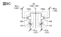
- 9A and 9B are diagrams illustrating a configuration example of a semiconductor device.
- FIG. 9C is an equivalent circuit diagram of the semiconductor device.
- FIG. 10 is a diagram showing a configuration example of a semiconductor device.
- FIG. 11 is an equivalent circuit diagram of the semiconductor device.
- FIG. 12 is a diagram showing a configuration example of a semiconductor device.
- FIG. 13 is an equivalent circuit diagram of the semiconductor device.
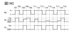
- FIG. 14A is a diagram illustrating an example of a circuit configuration of a memory cell.
- FIG. 14B is a graph showing an example of hysteresis characteristics.
- FIG. 14C is a timing chart showing an example of a method for driving a memory cell.
- 15A to 15C are diagrams showing configuration examples of storage devices.
- FIG. 16A is a diagram illustrating a configuration example of a storage device.
- FIG. 16A is a diagram illustrating a configuration example of a storage device.
- FIG. 16A is a diagram illustrating a configuration example of a storage device.
- FIG. 16A is a diagram illustrating a
- FIG. 16B is a schematic diagram of a memory string included in the storage device.
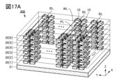
- FIG. 17A is a diagram illustrating a configuration example of a storage device.
- FIG. 17B is a schematic diagram of a memory string included in the storage device.
- FIG. 18 is a diagram showing an example of a cross-sectional configuration of a storage device.
- 19A and 19B are schematic diagrams of a semiconductor device according to one embodiment of the present invention.
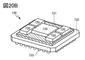
- 20A and 20B are perspective views showing an example of an electronic component.
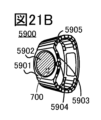
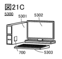
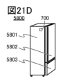
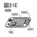
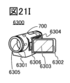
- 21A to 21J are diagrams illustrating an example of an electronic device.
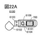
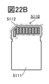
- 22A to 22E are diagrams illustrating an example of an electronic device.
- 23A to 23C are diagrams illustrating an example of an electronic device.
- FIG. 24 is a diagram showing an example of space equipment.
- a semiconductor device is a device that utilizes semiconductor characteristics, and refers to a circuit including a semiconductor element (transistor, diode, photodiode, etc.), a device having the same circuit, and the like. It also refers to any device that can function by utilizing the characteristics of semiconductors. For example, an integrated circuit, a chip including an integrated circuit, and an electronic component containing a chip in a package are examples of semiconductor devices. Furthermore, storage devices, display devices, light emitting devices, lighting devices, electronic devices, and the like are themselves semiconductor devices and may include semiconductor devices.
- arrows indicating the X direction (direction along the X axis), Y direction (direction along the Y axis), and Z direction (direction along the Z axis) may be provided.
- the "X direction” refers to the direction along the X axis, and there is no distinction between the forward direction and the reverse direction unless explicitly stated. The same applies to the "Y direction” and the "Z direction”.
- the X direction, the Y direction, and the Z direction are directions that intersect with each other. More specifically, the X direction, the Y direction, and the Z direction are directions that are orthogonal to each other.
- one of the X direction, the Y direction, or the Z direction may be referred to as a "first direction” or a “first direction.” Further, the other direction may be referred to as a “second direction” or “second direction”. Further, the remaining one may be referred to as a "third direction” or "third direction.”
- ordinal numbers such as “first,” “second,” and “third” are added to avoid confusion of constituent elements. Therefore, the number of components is not limited. Further, the order of the constituent elements is not limited. For example, a component referred to as “first” in one embodiment such as this specification is a component referred to as “second” in other embodiments, claims, etc. It is possible. Furthermore, for example, a component referred to as “first” in one of the embodiments of this specification etc. may be omitted in other embodiments or claims.
- electrode B does not need to be formed directly on insulating layer A, and there is no need to form another structure between insulating layer A and electrode B. Do not exclude things that contain elements.
- electrode B overlapping insulating layer A is not limited to the state in which electrode B is formed on insulating layer A, but also the state in which electrode B is formed under insulating layer A, or A state in which the electrode B is formed on the right side (or left side) of the insulating layer A is not excluded.
- the terms “adjacent” and “nearby” do not limit that components are in direct contact.
- insulating layer A and electrode B do not need to be formed in direct contact with each other, and other components may be placed between insulating layer A and electrode B. Do not exclude what is included.
- the term “conductive layer” or “conductive film” may be changed to the term “conductor.”
- the term “conductor” may be changed to the term “conductive layer” or “conductive film.”
- the term “insulating layer” or “insulating film” may be changed to the term “insulator.”
- the term “insulator” may be changed to the term “insulating layer” or “insulating film.”
- voltage refers to the potential difference between two points, and potential refers to the electrostatic energy (electrical potential energy) possessed by a unit charge in an electrostatic field at a certain point.
- a potential difference between a potential at a certain point and a reference potential is simply called a potential or a voltage, and potential and voltage are often used synonymously. Therefore, in this specification and the like, unless explicitly stated, a potential may be read as a voltage, and a voltage may be read as a potential.
- Electrode In this specification and the like, terms such as “electrode,” “wiring,” and “terminal” do not functionally limit these components.
- an “electrode” may be used as part of a “wiring” and vice versa.
- the term “electrode” or “wiring” includes cases where a plurality of “electrodes” or “wirings” are formed integrally.
- a “terminal” may be used as part of a “wiring” or “electrode,” and vice versa.
- the term “terminal” also includes cases where a plurality of "electrodes", “wirings", “terminals”, etc. are formed integrally.
- an “electrode” can be a part of a “wiring” or a “terminal,” and, for example, a “terminal” can be a part of a “wiring” or a “electrode.”
- terms such as “electrode,” “wiring,” and “terminal” may be replaced with terms such as "region” depending on the case.
- terms such as “wiring,” “signal line,” and “power line” can be interchanged depending on the situation or situation. For example, it may be possible to change the term “wiring” to the term “signal line.” Furthermore, for example, it may be possible to change the term “wiring” to a term such as “power line”. The reverse is also true, and terms such as “signal line” and “power line” may sometimes be changed to the term “wiring”. Terms such as “power line” may be changed to terms such as “signal line”. Moreover, the reverse is also true, and a term such as “signal line” may be changed to a term such as “power line”. Further, depending on the case or the situation, the term “potential” applied to the wiring may be changed to a term such as “signal”. Moreover, the reverse is also true, and a term such as “signal” may be changed to the term “potential”.
- a “capacitive element” refers to, for example, a circuit element having a capacitance value higher than 0F, a wiring region having a capacitance value higher than 0F, a parasitic capacitance, or It can be the gate capacitance of a transistor.
- capacitor element can sometimes be replaced with the term “capacitance.”
- capacitor may be translated into the terms “capacitive element,” “parasitic capacitance,” or “gate capacitance.”
- a “capacitor” (including a “capacitor” having three or more terminals) has a configuration including an insulator and a pair of conductors sandwiching the insulator.
- the term “pair of conductors” in “capacitance” can be paraphrased as “pair of electrodes,” “pair of conductive regions,” “pair of regions,” or “pair of terminals.” Further, the term “one of a pair of terminals” may also be referred to as “one terminal” or “first terminal.” Moreover, the term “the other of a pair of terminals” may be referred to as “the other terminal” or “the second terminal.” Note that the value of the capacitance can be, for example, 0.05 fF or more and 10 pF or less. Further, for example, it may be set to 1 pF or more and 10 ⁇ F or less.
- source and drain may be interchanged, such as when using transistors of different polarity or when the direction of current changes during circuit operation. Therefore, in this specification and the like, the terms “source” and “drain” can be used interchangeably.
- gate refers to part or all of a gate electrode and a gate wiring.
- the gate wiring refers to a wiring for electrically connecting the gate electrode of at least one transistor to another electrode or another wiring.
- source refers to part or all of a source region, a source electrode, and a source wiring.
- the source region refers to a region of the semiconductor layer where the resistivity is below a certain value.
- a source electrode refers to a conductive layer including a portion connected to a source region.
- the source wiring refers to a wiring for electrically connecting the source electrode of at least one transistor to another electrode or another wiring.
- drain refers to part or all of a drain region, a drain electrode, and a drain wiring.
- the drain region refers to a region of the semiconductor layer where the resistivity is below a certain value.
- a drain electrode refers to a conductive layer including a portion connected to a drain region.
- the drain wiring refers to a wiring for electrically connecting the drain electrode of at least one transistor to another electrode or another wiring.
- the transistors shown in this specification and the like are enhancement type (normally-off type) field effect transistors.
- the transistors described in this specification and the like are n-channel transistors, and unless otherwise specified, the threshold voltage (also referred to as "Vth") of the transistors is greater than 0V.
- the transistor shown in this specification and the like is a p-channel transistor, and unless otherwise specified, the threshold voltage (also referred to as "Vth”) of the transistor is 0V or less.
- the Vth of a plurality of transistors of the same conductivity type are all equal.
- off-state current refers to the current (current) that flows between the source and drain when the transistor is in the off state (also referred to as the "non-conducting state” or “blocking state”).
- drain current also referred to as “drain current” or “Id.”
- an off state is defined as an n-channel transistor in which the potential difference between the gate and source (also referred to as “gate voltage” or “Vg”) with respect to the source is lower than the threshold voltage.
- Vg gate voltage
- the off-state current of an n-channel transistor may refer to the drain current when Vg is lower than Vth.
- off-state current may refer to, for example, a current flowing between a source and a drain when a transistor is in an off state.
- on-current refers to Id when a transistor is in an on-state (also referred to as a "conductive state").
- the on-state refers to a state in which Vg is greater than or equal to Vth for an n-channel transistor, and a state in which Vg is less than or equal to Vth for a p-channel transistor.
- the on-current of an n-channel transistor may refer to the drain current when Vg is equal to or higher than Vth.
- parallel refers to a state in which two straight lines are arranged at an angle of -10 degrees or more and 10 degrees or less. Therefore, the case where the temperature is greater than or equal to -5 degrees and less than or equal to 5 degrees is also included.
- substantially parallel or “substantially parallel” refers to a state in which two straight lines are arranged at an angle of -30 degrees or more and 30 degrees or less.
- perpendicular refers to a state in which two straight lines are arranged at an angle of 80 degrees or more and 100 degrees or less. Therefore, cases where the angle is greater than or equal to 85 degrees and less than or equal to 95 degrees are also included.
- substantially perpendicular or “substantially perpendicular” refers to a state in which two straight lines are arranged at an angle of 60 degrees or more and 120 degrees or less.
- the conductive layer 242 may be shown divided into a conductive layer 242a and a conductive layer 242b.
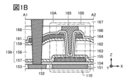
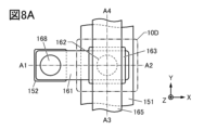
- FIG. 1A is a top view of a semiconductor device 10A.
- FIG. 1B is a cross-sectional view of the portion indicated by the dashed line A1-A2 in FIG. 1A, viewed from the Y direction. Note that in the top view of FIG. 1A, some elements are omitted for clarity.
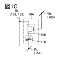
- FIGS. 1C and 1D show equivalent circuit diagrams of the semiconductor device 10A.
- one of the source and drain of the transistor 100 is electrically connected to the wiring BL, and the other is electrically connected to one electrode of the capacitor 110.
- a gate of the transistor 100 is electrically connected to the wiring WL.
- the other electrode of the capacitive element 110 is electrically connected to the wiring PL.
- the semiconductor device 10A functions as a memory circuit (also referred to as a "memory element” or "memory cell").
- FIG. 1C is an equivalent circuit diagram when the capacitive element 110 includes a ferroelectric material
- FIG. 1D is an equivalent circuit diagram when the capacitive element 110 does not include a ferroelectric material.
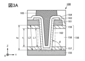
- FIG. 2A is a cross-sectional view of the portion indicated by the dashed line A3-A4 in FIG. 1A, viewed from the X direction.
- FIG. 2B is an enlarged cross-sectional view of the portion shown by the dashed line B1-B2 in FIG. 2A when viewed from the Z direction.
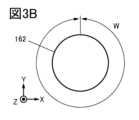
- FIG. 2C is an enlarged cross-sectional view of the portion shown by the dashed line B3-B4 in FIG. 2A when viewed from the Z direction.
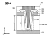
- a semiconductor device 10A of one embodiment of the present invention includes an insulating layer 153, and a conductive layer 151 and a conductive layer 152 that are embedded in the insulating layer 153.
- the conductive layer 151 and the conductive layer 152 can be formed at the same time using the same material and in the same manufacturing process. Further, it is preferable that the positions (positions in the Z direction) of the upper surfaces of the insulating layer 153, the conductive layer 151, and the conductive layer 152 match or substantially match using a chemical mechanical polishing (CMP) method or the like.
- CMP chemical mechanical polishing
- an insulating layer 154 is provided over the insulating layer 153, the conductive layer 151, and the conductive layer 152, and a conductive layer 155 is provided over the insulating layer 154.
- the conductive layer 151 and the conductive layer 155 have a region where they overlap with each other with the insulating layer 154 in between.
- the semiconductor device 10A has an insulating layer 157 on the insulating layer 154 and the conductive layer 155, an insulating layer 158 on the insulating layer 157, and an insulating layer 159 on the insulating layer 158.
- the insulating layer 157, the insulating layer 158, and the insulating layer 159 may be collectively referred to as the insulating layer 156 or a spacer layer.
- a conductive layer 161 is provided on the insulating layer 159.
- openings 162 are provided in the conductive layer 161, the insulating layer 159, the insulating layer 158, and the insulating layer 157 in a region overlapping with a part of the conductive layer 155 (see FIG. 1B and FIG. 2A).
- the semiconductor device 10A has a semiconductor layer 163 that covers the opening 162.
- the semiconductor layer 163 has a region that overlaps with the bottom of the opening 162 and a region that overlaps with the side surface of the opening 162. That is, the semiconductor layer 163 has a region in contact with the insulating layer 156.
- the semiconductor layer 163 has a region in contact with the side surface of the insulating layer 157, a region in contact with the side surface of the insulating layer 158, and a region in contact with the side surface of the insulating layer 159.
- the semiconductor layer 163 has a region in contact with the conductive layer 155 and a region in contact with the conductive layer 161. That is, a portion of the semiconductor layer 163 is electrically connected to the conductive layer 155, and another portion of the semiconductor layer 163 is electrically connected to the conductive layer 161. Further, the semiconductor layer 163 may have a region extending beyond the edge of the conductive layer 161 (see FIGS. 1A and 2A).
- an insulating layer 164 is provided over the insulating layer 159, the conductive layer 161, and the semiconductor layer 163. Further, a conductive layer 165 is provided on the insulating layer 164.
- the conductive layer 165 has a region that overlaps with the opening 162, and in this region, a region that overlaps with the side surface and bottom of the opening 162 via the insulating layer 164 and the semiconductor layer 163 (see FIG. 1B, FIG. 2A, FIG. 2B, and FIG. (See 2C).
- the thickness of the semiconductor layer 163 is preferably 1 nm or more, 3 nm or more, or 5 nm or more, and 20 nm or less, 15 nm or less, 12 nm or less, or 10 nm or less.
- the thickness of the insulating layer 164 is preferably 0.5 nm or more and 15 nm or less, more preferably 0.5 nm or more and 12 nm or less, and even more preferably 0.5 nm or more and 10 nm or less.
- the insulating layer 164 only needs to have a region with the thickness described above at least in part.
- an insulating layer 166 is provided on the insulating layer 164. It is preferable that the positions (positions in the Z direction) of the upper surfaces of the conductive layer 165 and the insulating layer 166 match or substantially match. For example, by performing CMP processing or the like, the positions of the upper surfaces of the conductive layer 165 and the insulating layer 166 (positions in the Z direction) are made to match or substantially match, thereby improving the coverage of the insulating layer and the conductive layer that will be formed later. can be increased.
- an insulating layer 167 is provided over the conductive layer 165 and the insulating layer 166. Further, in the region overlapping with the conductive layer 152, the conductive layer 167, the insulating layer 166, the insulating layer 164, the conductive layer 161, the insulating layer 159, the insulating layer 158, the insulating layer 157, and a part of the insulating layer 154 are embedded. It has a layer 168. Conductive layer 168 is electrically connected to conductive layer 161 and conductive layer 152. Conductive layer 168 and conductive layer 152 function as contact plugs.
- the conductive layer 155 functions as one electrode of the capacitive element 110.
- the conductive layer 151 functions as the other electrode of the capacitive element 110.
- a region of the insulating layer 154 overlapping with the conductive layer 155 and the conductive layer 151 functions as a dielectric of the capacitive element 110.
- Each of conductive layer 165 and conductive layer 151 extends in the Y direction.
- the conductive layer 165 functions as the wiring WL or a part of the wiring WL
- the conductive layer 151 functions as the wiring PL or a part of the wiring PL.
- the conductive layer 168 and the conductive layer 152 function as the wiring BL or a part of the wiring BL.
- a transistor 100 and a capacitor 110 are provided in an overlapping manner. By overlapping the transistor 100 and the capacitor 110, the area occupied by the semiconductor device 10A can be reduced.
- the conductive layer 161 functions as either a source electrode or a drain electrode of the transistor 100. Further, the conductive layer 155 functions as the other of the source electrode and the drain electrode of the transistor 100. For example, if the conductive layer 161 functions as a drain electrode of the transistor 100, the conductive layer 155 functions as a source electrode of the transistor 100. Note that the conductive layer 161 can also be said to function as the wiring BL or a part of the wiring BL.
- the semiconductor layer 163 functions as a semiconductor layer in which a channel of the transistor 100 is formed (a semiconductor layer including a channel formation region), the insulating layer 164 functions as a gate insulating layer, and the conductive layer 165 functions as a gate electrode. Therefore, it can be said that the transistor 100 is provided in a region including the opening 162.
- the transistor 100 has a source electrode and a drain electrode arranged in the Z direction. That is, the source and drain of the transistor 100 are arranged at different heights. In other words, the source and drain of the transistor 100 are arranged at different positions in the Z direction.
- Such a transistor is also referred to as a “vertical channel transistor,” “vertical channel transistor,” “vertical transistor,” or “VFET (Vertical Field Effect Transistor).”
- a source electrode and a drain electrode are arranged in the Z direction. That is, the channel formation region, the source region, and the drain region are arranged in the Z direction.
- the vertical transistor can reduce the area occupied by the transistor 100 compared to a conventional transistor in which a channel formation region, a source region, and a drain region are provided separately on the XY plane.
- the area occupied by the semiconductor device can be reduced.
- high integration of the semiconductor device can be achieved.
- the storage capacity per unit area of a storage device using the semiconductor device can be increased.
- the channel length is set by the exposure limit of photolithography.
- the channel length can be set by the thickness of the insulating layer 156 or the insulating layer 158. Therefore, the channel length of the transistor 100 is set to a very fine structure below the exposure limit of photolithography (for example, 60 nm or less, 50 nm or less, 40 nm or less, 30 nm or less, 20 nm or less, or 10 nm or less, but 1 nm or more, or 5 nm or more).
- the on-state current of the transistor 100 increases, and frequency characteristics can be improved.
- a vertical channel transistor a semiconductor device with high operating speed can be provided.
- ⁇ Capacitive element 110> A region where the conductive layer 151 and the conductive layer 155 overlap each other with the insulating layer 154 in between functions as the capacitive element 110. It is preferable to use a ferroelectric material for the insulating layer 154. Ferroelectric materials have the property that polarization occurs internally when an electric field is applied from the outside, and the polarization remains even when the electric field is reduced to zero. Therefore, a nonvolatile memory element can be realized using a capacitive element (also referred to as a "ferroelectric capacitor”) using this material as a dielectric.
- a capacitive element also referred to as a "ferroelectric capacitor
- the capacitive element 110 functions as a ferroelectric capacitor
- a material that easily causes polarization in the insulating layer 154 as the conductive layer 151 and the conductive layer 155 in contact with the insulating layer 154 which is a ferroelectric material.
- titanium nitride as the conductive layer 151 and the conductive layer 155.
- a nonvolatile memory element using a ferroelectric capacitor is sometimes called a "FeRAM” or a “ferroelectric memory.” Materials that can have ferroelectricity will be explained in detail later.
- a material with a high dielectric constant (also referred to as a "high-k material”) may be used for the insulating layer 154.
- a high-k material As the insulating layer 154, the capacitance necessary for the capacitive element 110 can be ensured, and the insulating layer 154 can be made thick.
- the dielectric strength voltage between the conductive layer 151 and the conductive layer 155 is increased, and electrostatic breakdown is suppressed. Therefore, the reliability of the capacitive element 110 is improved. Therefore, the reliability of the semiconductor device using the capacitor 110 is improved.
- the material used for the substrate there are no major restrictions on the material used for the substrate.
- the material may be determined by taking into account the presence or absence of translucency and heat resistance to withstand heat treatment.
- an insulating substrate, a semiconductor substrate, or a conductive substrate may be used.
- a glass substrate such as barium borosilicate glass or aluminoborosilicate glass
- a ceramic substrate such as barium borosilicate glass or aluminoborosilicate glass
- a ceramic substrate such as barium borosilicate glass or aluminoborosilicate glass
- a ceramic substrate such as barium borosilicate glass or aluminoborosilicate glass
- a ceramic substrate such as barium borosilicate glass or aluminoborosilicate glass
- a ceramic substrate such as barium borosilicate glass or aluminoborosilicate glass
- a ceramic substrate such as barium borosilicate glass or alumino
- the semiconductor substrate examples include a semiconductor substrate made of silicon or germanium, or a compound semiconductor substrate made of silicon carbide, silicon germanium, gallium arsenide, indium phosphide, zinc oxide, or gallium oxide. . Furthermore, there is a semiconductor substrate having an insulator region inside the semiconductor substrate described above, such as an SOI (Silicon On Insulator) substrate. Furthermore, the semiconductor substrate may be a single crystal semiconductor or a polycrystalline semiconductor.
- the conductive substrate examples include a graphite substrate, a metal substrate, an alloy substrate, and a conductive resin substrate.
- substrates containing metal nitrides examples include substrates containing metal oxides, and the like.
- substrates in which an insulator substrate is provided with a conductor or a semiconductor a semiconductor substrate in which a conductor or an insulator is provided, and a conductor substrate in which a semiconductor or an insulator is provided.
- polyester resins such as polyethylene terephthalate (PET) and polyethylene naphthalate (PEN), polyacrylonitrile resins, acrylic resins, polyimide resins, polymethyl methacrylate resins, and polycarbonate (PC).
- PET polyethylene terephthalate
- PEN polyethylene naphthalate
- PC polycarbonate
- ) resin polyethersulfone (PES) resin, polyamide resin (nylon, aramid, etc.), polysiloxane resin, cycloolefin resin, polystyrene resin, polyamideimide resin, polyurethane resin, polyvinyl chloride resin, polyvinylidene chloride resin, polypropylene resin , polytetrafluoroethylene (PTFE) resin, ABS resin, cellulose nanofiber, etc.
- PET polyethylene terephthalate
- PEN polyethylene naphthalate
- PES polyethersulfone
- PEN polyamide resin
- polystyrene resin polyamide
- a lightweight semiconductor device including the transistor 100 can be provided. Furthermore, by using the above material as a substrate, a semiconductor device that is resistant to impact can be provided. Further, by using the above material as a substrate, a semiconductor device that is less likely to be damaged can be provided.
- these substrates provided with elements may be used.
- Elements provided on the substrate include capacitive elements, resistive elements, switch elements, light emitting elements, and memory elements.
- an insulating oxide, nitride, oxynitride, nitride oxide, metal oxide, metal oxynitride, metal nitride oxide, or the like can be used.
- An insulating material selected from lanthanum, neodymium oxide, hafnium oxide, tantalum oxide, aluminum silicate, etc. is used in a single layer or in a stacked manner.
- a mixture of a plurality of materials among oxide materials, nitride materials, oxynitride materials, and nitrided oxide materials may be used.
- nitrided oxide refers to a material containing more nitrogen than oxygen.
- oxynitride refers to a material containing more oxygen than nitrogen. Note that the content of each element can be measured using, for example, Rutherford Backscattering Spectrometry (RBS).
- RBS Rutherford Backscattering Spectrometry
- gate insulating layers become thinner, which may cause problems such as leakage current.
- a high-k material high dielectric constant material, material with high relative permittivity
- the insulating layer a material having a high dielectric constant such as lead zirconate titanate (PZT), strontium titanate (SrTiO 3 ), (Ba,Sr)TiO 3 (BST) may be used in some cases.
- PZT lead zirconate titanate
- SBa,Sr)TiO 3 BST
- the material should be selected depending on the function required of the insulating layer.
- Materials with high dielectric constants include gallium oxide, hafnium oxide, zirconium oxide, oxides containing aluminum and hafnium, oxynitrides containing aluminum and hafnium, oxides containing silicon and hafnium, and oxides containing silicon and hafnium. These include oxynitrides or nitrides with silicon and hafnium.
- materials with low dielectric constants include silicon oxide, silicon oxynitride, silicon nitride oxide, silicon nitride, silicon oxide with fluorine added, silicon oxide with carbon added, silicon oxide with carbon and nitrogen added, and vacancies.
- silicon oxides and resins that have
- the method for forming the insulating material is not particularly limited, and various methods such as vapor deposition, ALD, CVD, sputtering, and spin coating can be used.
- the insulating layer 153 and the insulating layer 167 are preferably formed using an insulating material through which impurities hardly pass.
- insulating materials containing boron, carbon, nitrogen, oxygen, fluorine, magnesium, aluminum, silicon, phosphorous, chlorine, argon, gallium, germanium, yttrium, zirconium, lanthanum, neodymium, hafnium or tantalum, in a single layer or It may be used in a laminated manner.
- Examples of insulating materials that are difficult for impurities to pass through include aluminum oxide, aluminum nitride, aluminum oxynitride, aluminum nitride oxide, gallium oxide, germanium oxide, yttrium oxide, zirconium oxide, lanthanum oxide, neodymium oxide, hafnium oxide, tantalum oxide, Examples include silicon nitride.
- an insulating layer that can function as a planarization layer may be used as the insulating layer.
- materials that function as the flattening layer include acrylic resin, polyimide, epoxy resin, polyamide, polyimide amide, siloxane resin, benzocyclobutene resin, phenol resin, and precursors thereof.
- low-k materials low dielectric constant materials, materials with small dielectric constants
- siloxane resins PSG (phosphorus glass), BPSG (phosphorus boron glass), etc.
- a plurality of insulating layers formed of these materials may be stacked.
- the siloxane resin corresponds to a resin containing Si-O-Si bonds formed using a siloxane-based material as a starting material.
- an organic group for example, an alkyl group or an aryl group
- a fluoro group may be used as a substituent. Further, the organic group may have a fluoro group.
- insulating layer 154 that functions as a dielectric of the capacitive element 110
- three insulating layers also referred to as "ZAZ" in which aluminum oxide is sandwiched between two layers of zirconium oxide may be used.
- ZAZ is a material with a high dielectric constant, and by using ZAZ as the dielectric of the capacitive element 110, the area occupied by the capacitive element 110 can be reduced.
- the capacitive element 110 functions as a ferroelectric capacitor.
- hafnium oxide as the material that can have ferroelectricity.
- a metal oxide such as zirconium oxide or HfZrOx ( X is a real number larger than 0; hereinafter also referred to as "HfZrOx" may be used as a material that can have ferroelectricity.
- hafnium oxide can be combined with element J1 (here, element J1 is zirconium (Zr), silicon (Si), aluminum (Al), gadolinium (Gd), yttrium (Y), A material to which one or more selected from lanthanum (La), strontium (Sr), etc. is added may be used.
- the ratio of the number of atoms of hafnium atoms and element J1 can be set as appropriate.
- the number of hafnium atoms and zirconium atoms may be set to 1:1 or around 1:1.
- materials that can have ferroelectricity include zirconium oxide and element J2 (here, element J2 is hafnium (Hf), silicon (Si), aluminum (Al), gadolinium (Gd), yttrium (Y)). , lanthanum (La), strontium (Sr), etc.) can be used.
- the ratio of the number of atoms of zirconium atoms and element J2 can be set as appropriate, for example, the number of atoms of zirconium atoms and element J2 may be set to 1:1 or around 1:1.
- materials that can have ferroelectricity lead titanate (PbTiO x ), barium strontium titanate (BST), strontium titanate, lead zirconate titanate (PZT), strontium bismuthate tantalate (SBT), Piezoelectric ceramics having a perovskite structure, such as bismuth ferrite (BFO) and barium titanate, may also be used.
- materials that can have ferroelectricity include aluminum scandium nitride (Al 1-a Sc a N b (a is a real number greater than 0 and less than 0.5, and b is a value of 1 or a value near it). (hereinafter simply referred to as AlScN)), Al-Ga-Sc nitride, Ga-Sc nitride, etc. can be used.
- AlScN aluminum scandium nitride
- Al-Ga-Sc nitride Al-Ga-Sc nitride
- Ga-Sc nitride etc.
- a metal nitride containing element M1, element M2, and nitrogen can be used as a material that can have ferroelectricity.
- the element M1 is one or more selected from aluminum (Al), gallium (Ga), indium (In), and the like.
- Element M2 is boron (B), scandium (Sc), yttrium (Y), lanthanoids (lanthanum (La), cerium (Ce), praseodymium (Pr), neodymium (Nd), promethium (Pm), samarium ( Sm), europium (Eu), gadolinium (Gd), terbium (Tb), dysprosium (Dy), holmium (Ho), erbium (Er), thulium (Tm), ytterbium (Yb), and lutetium (Lu)), Actinides (15 elements from actinium (Ac) to lawrenium (Lr)), titanium (Ti), zirconium (Zr), hafnium (Hf), vanadium (V), niobium (Nb), tantalum (Ta), chromium ( Cr), etc.
- Actinides (15 elements from actinium (Ac) to lawrenium (Lr)), titanium (Ti
- the ratio between the number of atoms of element M1 and the number of atoms of element M2 can be set as appropriate.
- a metal oxide containing element M1 and nitrogen may have ferroelectricity even if it does not contain element M2.
- a material that can have ferroelectricity a material obtained by adding element M3 to the metal nitride described above can be used.
- the element M3 is one or more selected from magnesium (Mg), calcium (Ca), strontium (Sr), zinc (Zn), cadmium (Cd), and the like.
- the ratio of the number of atoms of element M1, the number of atoms of element M2, and the number of atoms of element M3 can be set as appropriate.
- the metal nitride contains at least a group 13 element and nitrogen, which is a group 15 element
- the metal nitride can be used as a group 13-15 ferroelectric material or a group 13 nitride ferroelectric material. Sometimes called dielectric.
- perovskite oxynitrides such as SrTaO 2 N and BaTaO 2 N, GaFeO 3 having a ⁇ alumina structure, and the like can be used.
- the material that can have ferroelectricity for example, a mixture or compound consisting of a plurality of materials selected from the materials listed above can be used.
- the material capable of having ferroelectricity may have a laminated structure made of a plurality of materials selected from the materials listed above.
- materials that exhibit ferroelectricity are referred to as In addition to being called a material, it is also called a material that can have ferroelectric properties or a material that has ferroelectric properties.
- hafnium oxide or a material containing hafnium oxide and zirconium oxide can have ferroelectricity even when processed into a thin film of several nm. Therefore, it is suitable.
- the thickness of the insulating layer 154 is preferably 100 nm or less, more preferably 50 nm or less, even more preferably 20 nm or less, and even more preferably 10 nm or less (typically 2 nm or more and 9 nm or less).
- the thickness of the insulating layer 154 is preferably 8 nm or more and 12 nm or less.
- AlScN aluminum scandium nitride
- AlScN aluminum scandium nitride
- AlScN aluminum scandium nitride
- the film thickness of the material that can have ferroelectricity can be 100 nm or less, preferably 50 nm or less, more preferably 20 nm or less, and still more preferably 10 nm or less (typically 2 nm or more and 9 nm or less). .
- the film thickness is preferably 8 nm or more and 12 nm or less.
- a material that can have ferroelectricity is sometimes referred to as a ferroelectric material.
- a layered material that can have ferroelectric properties is sometimes referred to as a ferroelectric layer, a metal oxide film, or a metal nitride film.
- a device having such a ferroelectric layer, metal oxide film, or metal nitride film may be referred to as a ferroelectric device in this specification and the like.
- HfZrOx when used as a material that can have ferroelectricity, it is preferable to form a film using an ALD method, particularly a thermal ALD method. Further, when forming a film of a material that can have ferroelectricity using a thermal ALD method, it is preferable to use a material that does not contain hydrocarbon (also referred to as HC) as a precursor. When a material that can have ferroelectric properties contains one or both of hydrogen and carbon, crystallization of the material that can have ferroelectric properties may be inhibited. Therefore, as described above, it is preferable to reduce the concentration of one or both of hydrogen and carbon in a material that can have ferroelectric properties by using a precursor that does not contain hydrocarbons.
- examples of precursors that do not contain hydrocarbons include chlorine-based materials.
- HfZrOx hafnium oxide and zirconium oxide
- HfCl 4 and/or ZrCl 4 may be used as the precursor.
- a dopant typically silicon, carbon, etc.
- a forming method using a material containing a hydrocarbon as a precursor may be used as one means for adding carbon as a dopant.
- the impurity concentration of the material that can have ferroelectricity is low.
- lower concentrations of hydrogen (H) and carbon (C) are more preferable.
- the hydrogen concentration of the material that can have ferroelectricity is preferably 5 ⁇ 10 20 atoms/cm 3 or less, more preferably 1 ⁇ 10 20 atoms/cm 3 or less.
- the carbon concentration of the material that can have ferroelectricity is preferably 5 ⁇ 10 19 atoms/cm 3 or less, more preferably 1 ⁇ 10 19 atoms/cm 3 or less.
- HfZrOx is used as a material that can have ferroelectricity
- H 2 O or O 3 can be used as the oxidizing agent.
- the oxidizing agent for ALD is not limited to this.
- the oxidizing agent in the ALD method may include one or more selected from O 2 , O 3 , N 2 O, NO 2 , H 2 O, and H 2 O 2 .
- a material that can have ferroelectricity it is preferable to have a rectangular crystal structure because it exhibits ferroelectricity.
- other crystal structures may be included.
- it may have one or more crystal structures selected from cubic, tetragonal, and monoclinic.
- a layer for increasing crystallinity may be formed before forming the material that can have ferroelectricity.
- a metal oxide such as hafnium oxide or zirconium oxide, or hafnium or zirconium can be used as the layer that increases crystallinity.
- AlScN is used as a material that can have ferroelectricity
- other crystal structures may be included in addition to the hexagonal crystal structure.
- a metal nitride such as aluminum nitride or scandium nitride, or aluminum or scandium.
- the layer for increasing crystallinity may be formed after forming the material that can have ferroelectricity.
- the material that can have ferroelectricity may have a composite structure having an amorphous structure and a crystalline structure.
- Conductive materials used for conductive layers such as various wirings and electrodes that make up semiconductor devices include aluminum (Al), chromium (Cr), copper (Cu), silver (Ag), gold (Au), platinum (Pt), Tantalum (Ta), nickel (Ni), titanium (Ti), molybdenum (Mo), tungsten (W), hafnium (Hf), vanadium (V), niobium (Nb), manganese (Mn), magnesium (Mg), A metal element selected from zirconium (Zr), beryllium (Be), etc., an alloy containing the above-mentioned metal elements, an alloy containing a combination of the above-mentioned metal elements, etc. can be used.
- tantalum nitride, titanium nitride, nitrides containing titanium and aluminum, nitrides containing tantalum and aluminum, ruthenium oxide, ruthenium nitride, oxides containing strontium and ruthenium, and oxides containing lanthanum and nickel are difficult to oxidize.
- a conductive material or a material that maintains conductivity even if it absorbs oxygen.
- a semiconductor having high electrical conductivity typified by polycrystalline silicon containing an impurity element such as phosphorus, or a silicide such as nickel silicide may be used.
- the method for forming the conductive material is not particularly limited, and various methods such as vapor deposition, atomic layer deposition (ALD), CVD, sputtering, and spin coating can be used.
- a Cu-X alloy (X is Mn, Ni, Cr, Fe, Co, Mo, Ta, or Ti) may be applied as the conductive material. Since the layer formed of the Cu-X alloy can be processed by a wet etching process, it is possible to suppress manufacturing costs.
- an aluminum alloy containing one or more elements selected from titanium, tantalum, tungsten, molybdenum, chromium, neodymium, and scandium may be used as the conductive material.
- conductive materials that can be used for the conductive layer indium tin oxide, indium oxide containing tungsten oxide, indium zinc oxide containing tungsten oxide, indium oxide containing titanium oxide, indium tin containing titanium oxide, etc.
- Conductive materials with oxygen can also be used, such as oxides, indium zinc oxide, indium tin oxide doped with silicon oxide.
- conductive materials containing nitrogen such as titanium nitride, tantalum nitride, and tungsten nitride can also be used.
- the conductive layer can also have a laminated structure in which a conductive material containing oxygen, a conductive material containing nitrogen, and a material containing the metal element described above are appropriately combined.
- the conductive layer may have a single-layer structure of an aluminum layer containing silicon, a two-layer structure in which a titanium layer is stacked on an aluminum layer, a two-layer structure in which a titanium layer is stacked on a titanium nitride layer, or a tungsten layer on a titanium nitride layer.
- a two-layer structure in which a tungsten layer is laminated on a tantalum nitride layer a two-layer structure in which a tungsten layer is laminated on a tantalum nitride layer, and a three-layer structure in which a titanium layer is laminated, an aluminum layer is laminated on the titanium layer, and a titanium layer is laminated on top of that. good.
- a plurality of conductive layers formed of the above-mentioned conductive materials may be laminated and used.
- the conductive layer may have a laminated structure in which a material containing the aforementioned metal element and a conductive material containing oxygen are combined.
- a laminated structure may be used in which a material containing the aforementioned metal element and a conductive material containing nitrogen are combined.
- a layered structure may be used in which a material containing the metal element described above, a conductive material containing oxygen, and a conductive material containing nitrogen are combined.
- a conductive layer is formed by laminating a conductive layer containing copper on a conductive layer containing at least one of indium or zinc and oxygen, and further laminating a conductive layer containing at least one of indium or zinc and oxygen on top of the conductive layer containing at least one of indium or zinc and oxygen. It may also have a three-layer structure. In this case, it is preferable that the side surfaces of the conductive layer containing copper are also covered with a conductive layer containing at least one of indium or zinc and oxygen. Further, for example, a plurality of conductive layers containing at least one of indium or zinc and oxygen may be stacked and used as the conductive layer.
- the capacitive element 110 functions as a ferroelectric capacitor
- a material that easily causes polarization in the insulating layer 154 as the conductive layer 151 and the conductive layer 155 in contact with the insulating layer 154 which is a ferroelectric material.
- titanium nitride as the conductive layer 151 and the conductive layer 155.
- semiconductor layer 163 As the semiconductor layer 163, a single crystal semiconductor, a polycrystalline semiconductor, a microcrystalline semiconductor, an amorphous semiconductor, or the like can be used alone or in combination.
- semiconductor material silicon, germanium, etc. can be used, for example.
- a compound semiconductor such as silicon germanium, silicon carbide, gallium arsenide, or a nitride semiconductor may be used.
- an organic substance having semiconductor properties or a metal oxide having semiconductor properties also referred to as an oxide semiconductor
- these semiconductor materials may contain impurities as dopants.
- the semiconductor layer 163 may be made of single crystal silicon, polycrystalline silicon, microcrystalline silicon, or amorphous silicon.
- polycrystalline silicon for example, low temperature polysilicon (LTPS) may be used.
- a transistor using amorphous silicon for the semiconductor layer 163 can be formed over a large glass substrate and can be manufactured at low cost.
- a transistor using polycrystalline silicon for the semiconductor layer 163 has high field effect mobility and can operate at high speed.
- a transistor using microcrystalline silicon for the semiconductor layer 163 has higher field effect mobility than a transistor using amorphous silicon, and can operate at high speed.
- the semiconductor layer 163 may include a layered material that functions as a semiconductor.
- a layered material is a general term for a group of materials having a layered crystal structure.
- a layered crystal structure is a structure in which layers formed by covalent bonds or ionic bonds are laminated via bonds that are weaker than covalent bonds or ionic bonds, such as van der Waals forces.
- a layered material has high electrical conductivity within a unit layer, that is, high two-dimensional electrical conductivity. By using a material that functions as a semiconductor and has high two-dimensional electrical conductivity for the channel formation region, a transistor with high on-state current can be provided.
- Examples of the layered material include graphene, silicene, and chalcogenide.
- a chalcogenide is a compound containing chalcogen (an element belonging to Group 16).
- examples of chalcogenides include transition metal chalcogenides, group 13 chalcogenides, and the like.
- transition metal chalcogenides that can be used as semiconductor layers of transistors include molybdenum sulfide (typically MoS 2 ), molybdenum selenide (typically MoSe 2 ), and molybdenum tellurium (typically MoTe 2 ) .
- tungsten sulfide typically WS 2
- tungsten selenide typically WSe 2
- tungsten tellurium typically WTe 2
- hafnium sulfide typically HfS 2
- hafnium selenide typically HfSe 2
- zirconium sulfide typically ZrS 2
- zirconium selenide typically ZrSe 2
- an oxide semiconductor has a band gap of 2 eV or more
- a transistor (also referred to as an "OS transistor") using an oxide semiconductor, which is a type of metal oxide, for the semiconductor layer in which a channel is formed has an off-state current of are significantly less. Therefore, power consumption of a semiconductor device including an OS transistor can be reduced.
- the OS transistor operates stably even in a high-temperature environment, with little variation in characteristics. For example, the off-state current hardly increases even in a high-temperature environment. Specifically, the off-state current hardly increases even under an environmental temperature of room temperature or higher and 200° C. or lower. Furthermore, the on-state current is less likely to decrease even in a high-temperature environment. Therefore, a semiconductor device including an OS transistor operates stably even in a high-temperature environment and has high reliability.
- the refresh operation frequency needs to be approximately 1 time/60 msec, but in the storage device of one embodiment of the present invention, the refresh operation frequency is approximately 1 time/10 sec, and 10 msec.
- the refresh operation frequency can be set to be twice or more or 100 times or more. Note that with the storage device of one embodiment of the present invention, the refresh operation can be performed once every 1 sec or more and 100 sec or less, preferably once every 5 sec or more and 50 sec or less.
- an OS transistor as the transistor 100. Since the OS transistor has a high dielectric strength voltage between the source and the drain, the channel length can be shortened. Therefore, the on-state current can be increased.
- the OS transistor is suitable for a vertical channel type transistor.
- the metal oxide contains at least indium (In) or zinc (Zn).
- the metal oxide has two or three selected from indium, element M, and zinc.
- the element M is a metal element or a metalloid element that has a high bonding energy with oxygen, for example, a metal element or a metalloid element that has a higher bonding energy with oxygen than indium.
- the element M includes aluminum, gallium, tin, yttrium, titanium, vanadium, chromium, manganese, iron, cobalt, nickel, zirconium, molybdenum, hafnium, tantalum, tungsten, lanthanum, cerium, neodymium, magnesium, and calcium. , strontium, barium, boron, silicon, germanium, and antimony.
- the element M included in the metal oxide is preferably one or more of the above elements, more preferably one or more selected from aluminum, gallium, tin, and yttrium, and further gallium. preferable. Note that in this specification and the like, metal elements and metalloid elements may be collectively referred to as "metal elements," and the "metal elements" described in this specification and the like may include semimetal elements.
- indium zinc oxide In-Zn oxide
- indium tin oxide In-Sn oxide
- indium titanium oxide In-Ti oxide
- indium gallium oxide In-Ga oxide
- Indium gallium aluminum oxide Indium gallium aluminum oxide
- indium gallium tin oxide In-Ga-Sn oxide
- gallium zinc oxide Ga-Zn oxide, also referred to as "GZO”
- aluminum Zinc oxide Al-Zn oxide, also written as "AZO”
- indium aluminum zinc oxide In-Al-Zn oxide, also written as "IAZO”
- indium tin zinc oxide In-Sn- Zn oxide
- indium titanium zinc oxide In-Ti-Zn oxide
- indium gallium tin zinc oxide In-Ga-Sn-Zn oxide, also written as "IGZTO”
- indium gallium aluminum zinc oxide In-Ga-
- the field effect mobility of the transistor can be increased.
- the metal oxide may include one or more metal elements having a large number of periods instead of indium.
- the metal oxide may contain one or more metal elements having a large number of periods in addition to indium. The greater the overlap between the orbits of the metal elements, the greater the carrier conduction in the metal oxide tends to be. Therefore, by including a metal element with a large number of periods, the field effect mobility of the transistor may be increased. Examples of metal elements having a large number of periods include metal elements belonging to the fifth period and metal elements belonging to the sixth period.
- the metal element examples include yttrium, zirconium, silver, cadmium, tin, antimony, barium, lead, bismuth, lanthanum, cerium, praseodymium, neodymium, promethium, samarium, and europium. Note that lanthanum, cerium, praseodymium, neodymium, promethium, samarium, and europium are called light rare earth elements.
- the metal oxide may contain one or more types of nonmetallic elements.
- the metal oxide contains a nonmetal element, the field effect mobility of the transistor can be increased in some cases.
- nonmetallic elements include carbon, nitrogen, phosphorus, sulfur, selenium, fluorine, chlorine, bromine, and hydrogen.
- the metal oxide becomes highly crystalline, and impurities in the metal oxide can be reduced. It can suppress the spread. Therefore, fluctuations in the electrical characteristics of the transistor are suppressed, and reliability can be improved.
- the electrical characteristics and reliability of a transistor vary depending on the composition of the metal oxide applied to the semiconductor layer. Therefore, by varying the composition of the metal oxide depending on the electrical characteristics and reliability required of the transistor, a semiconductor device that has both excellent electrical characteristics and high reliability can be realized.
- a metal oxide in which the atomic ratio of indium is greater than or equal to the atomic ratio of zinc may be used.
- a metal oxide in which the atomic ratio of indium is greater than or equal to the atomic ratio of tin may be used.
- a metal oxide in which the atomic ratio of indium is higher than the atomic ratio of tin may be used. Furthermore, it is preferable to use a metal oxide in which the atomic ratio of zinc is higher than the atomic ratio of tin.
- a metal oxide in which the atomic ratio of indium is higher than the atomic ratio of aluminum may be used. Furthermore, it is preferable to use a metal oxide in which the atomic ratio of zinc is higher than that of aluminum.
- the atomic ratio of indium to the sum of the number of atoms of metal elements contained in the In-Ga-Zn oxide is higher than the atomic ratio of gallium.
- Metal oxides may also be used.
- the atomic ratio of indium to the sum of the number of atoms of metal elements contained in the In-M-Zn oxide is higher than the atomic ratio of element M.
- High metal oxides may also be used.
- the nearby composition includes a range of ⁇ 30% of the desired atomic ratio.
- the element M it is preferable to use gallium.
- the sum of the atomic ratios of the metal elements can be the atomic ratio of the element M.
- the atomic ratio of the element M can be the sum of the atomic ratio of gallium and the atomic ratio of aluminum.
- the atomic ratio of indium, element M, and zinc is within the above range.
- the ratio of the number of atoms of indium to the sum of the number of atoms of metal elements is 30 atom % or more and 100 atom % or less, preferably 30 atom % or more and 95 atom % or less, more preferably is from 35 atom % to 95 atom %, more preferably from 35 atom % to 90 atom %, more preferably from 40 atom % to 90 atom %, more preferably from 45 atom % to 90 atom %, more preferably from 50 atom % to 90 atom %.
- the ratio of the number of indium atoms to the total number of atoms of indium, element M, and zinc is within the above range.
- the field effect mobility of the transistor can be increased by increasing the ratio of the number of indium atoms to the sum of the number of atoms of the metal elements.
- a circuit that can operate at high speed can be manufactured. Furthermore, it becomes possible to reduce the area occupied by the circuit.
- the analysis of the composition of the composition of metal oxides for example, the energy distributed X -ray optical method (EDX: ENERGY DISPERSIVE X -RAY SPECTROSCOPY), X -ray optical electron division of light (XPS: X -Ray PhotoElECTRON SPECTROSCOP). Y), guidance bond plasma mass analysis method (ICP-MS: Inductively Coupled Plasma-Mass Spectrometry), or Inductively Coupled Plasma-Atomic Emis (ICP-AES) sion Spectrometry) can be used. Alternatively, analysis may be performed by combining two or more of these methods. Note that for elements with low content rates, the actual content rate and the content rate obtained by analysis may differ due to the influence of analysis accuracy. For example, when the content of element M is low, the content of element M obtained by analysis may be lower than the actual content.
- a sputtering method or an atomic layer deposition (ALD) method can be suitably used to form the metal oxide.
- the atomic ratio of the target and the atomic ratio of the metal oxide may be different.
- the atomic ratio of the metal oxide may be smaller than the atomic ratio of the target.
- the atomic ratio of zinc contained in the target may be about 40% or more and 90% or less.
- the above atomic ratio is not limited to the atomic ratio of the formed metal oxide, but also the atomic ratio of the sputtering target used for forming the metal oxide film. It may be.
- GBT Gate Bias Temperature
- PBTS Positive Bias Temperature Stress
- NBTS Negative Bias Temperature Stress
- PBTS test and NBTS test performed under light irradiation are respectively PBTIS (Positive Bias Temperature Illumination Stress) test and NBTIS (Negative Bias Temperature I) test. Illumination Stress) test.
- n-type transistors In n-type transistors, a positive potential is applied to the gate when the transistor is turned on, so the amount of variation in threshold voltage in the PBTS test is an important indicator of transistor reliability. This is one of the items.
- a transistor with high reliability against application of a positive bias can be obtained.
- a transistor with a small threshold voltage variation in the PBTS test can be obtained.
- the gallium content is lower than the indium content.
- One of the factors that causes the threshold voltage to fluctuate in the PBTS test is the defect level at or near the interface between the semiconductor layer and the gate insulating layer.
- gallium contained in metal oxides has a property of attracting oxygen more easily than other metal elements (for example, indium or zinc). Therefore, it is presumed that at the interface between the metal oxide containing a large amount of gallium and the gate insulating layer, gallium combines with excess oxygen in the gate insulating layer, making it easier to generate carrier (electron in this case) trap sites. . Therefore, when a positive potential is applied to the gate, carriers are trapped at the interface between the semiconductor layer and the gate insulating layer, which may cause the threshold voltage to fluctuate.
- a metal oxide in which the atomic ratio of indium is higher than the atomic ratio of gallium can be applied to the semiconductor layer.
- a metal oxide in which the atomic ratio of zinc is higher than the atomic ratio of gallium it is preferable to apply a metal oxide in which the atomic ratio of metal elements satisfies In>Ga and Zn>Ga to the semiconductor layer.
- the ratio of the number of gallium atoms to the number of atoms of the metal element contained is greater than 0 atom % and less than 50 atom %, preferably from 0.1 atom % to 40 atom %, more preferably 0.1 atomic % or more and 35 atomic % or less, more preferably 0.1 atomic % or more and 30 atomic % or less, more preferably 0.1 atomic % or more and 25 atomic % or less, more preferably 0.1 atomic % or more and 20 atomic % or less % or less, more preferably 0.1 atomic % or more and 15 atomic % or less, more preferably 0.1 atomic % or more and 10 atomic % or less.
- V O oxygen vacancy
- a metal oxide that does not contain gallium may be applied to the semiconductor layer of the OS transistor.
- In--Zn oxide can be applied to the semiconductor layer.
- the field effect mobility of the transistor can be increased by increasing the ratio of the number of atoms of indium to the number of atoms of the metal element contained in the metal oxide.
- the metal oxide becomes highly crystalline, which suppresses fluctuations in the electrical characteristics of the transistor and increases reliability. be able to.
- a metal oxide that does not contain gallium and zinc, such as indium oxide may be applied to the semiconductor layer. By using a metal oxide that does not contain gallium, it is possible to make threshold voltage fluctuations extremely small, especially in PBTS tests.
- an oxide containing indium and zinc can be used for the semiconductor layer.
- the present invention can also be applied to a case where element M is used instead of gallium. It is preferable to use a metal oxide in which the atomic ratio of indium is higher than the atomic ratio of element M to the semiconductor layer. Further, it is preferable to use a metal oxide in which the atomic ratio of zinc is higher than the atomic ratio of element M.
- the semiconductor layer may have a stacked structure having two or more metal oxide layers.
- the two or more metal oxide layers included in the semiconductor layer may have the same or approximately the same composition.
- the same sputtering target can be used to form the layers, thereby reducing manufacturing costs.
- the two or more metal oxide layers included in the semiconductor layer may have different compositions.
- a first metal oxide layer having a composition of In:M:Zn 1:3:4 [atomic ratio] or a composition close to that, and In:M:Zn provided on the first metal oxide layer.
- a laminated structure with a second metal oxide layer having an atomic ratio of 1:1:1 or a composition close to this can be suitably used.
- gallium or aluminum as the element M.
- a first metal oxide layer having a composition of In:M:Zn 1:1:1 [atomic ratio] or a composition close to that, and an In:Zn layer provided on the first metal oxide layer.
- a metal oxide layer having crystallinity As the semiconductor layer, a metal oxide layer having crystallinity can be used.
- a metal oxide layer having a CAAC (c-axis aligned crystal) structure, a polycrystalline structure, a microcrystalline (NC: nano-crystal) structure, etc. can be used.
- a crystalline metal oxide layer As a semiconductor layer, the density of defect levels in the semiconductor layer can be reduced, and a highly reliable display device can be realized.
- the semiconductor layer of the OS transistor may have a stacked structure of two or more metal oxide layers having different crystallinity.
- the layered structure includes a first metal oxide layer and a second metal oxide layer provided on the first metal oxide layer, and the second metal oxide layer
- the structure can include a region having higher crystallinity than the oxide layer.
- the second metal oxide layer may have a region having lower crystallinity than the first metal oxide layer.
- the two or more metal oxide layers included in the semiconductor layer may have the same or approximately the same composition.
- a stacked structure of two or more metal oxide layers having different crystallinity can be formed.
- the two or more metal oxide layers included in the semiconductor layer may have different compositions.
- a material containing hydrogen is preferably used for the insulating layer 157 and the insulating layer 159.
- the oxide semiconductor in the region in contact with the insulating layer is made n-type and can function as a source region or a drain region.
- a material containing silicon, nitrogen, and hydrogen may be used as the insulating layer.
- silicon nitride containing hydrogen, silicon nitride oxide containing hydrogen, or the like may be used.
- the thickness of the insulating layer 157 and the insulating layer 159 is preferably 1 nm or more and 15 nm or less, more preferably 2 nm or more and 10 nm or less, more preferably 3 nm or more and 7 nm or less, and further preferably 3 nm or more and 5 nm or less.
- an oxide semiconductor is used for the semiconductor layer 163
- a region of the semiconductor layer 163 in contact with the insulating layer 157 containing hydrogen and a region in contact with the insulating layer 159 containing hydrogen function as a source region or a drain region.
- the thickness of the insulating layer 158 is preferably 1 nm or more and 50 nm or less, more preferably 2 nm or more and 30 nm or less, and even more preferably 3 nm or more and 2 nm or less.
- the thicknesses of the insulating layer 157, the insulating layer 158, and the insulating layer 159 may be appropriately set according to the characteristics required of the transistor 100.
- the insulating layer 157, the insulating layer 158, and the insulating layer 159 be formed successively without being exposed to the atmospheric environment midway.
- the interface between the insulating layer 157 and the insulating layer 158 and its vicinity, as well as the insulating layer 158 and Impurities or moisture from the atmospheric environment can be prevented from adhering to the interface of the insulating layer 159 and its vicinity.
- the conductive layer 155 in contact with the semiconductor layer 163 and the conductive layer 161 in contact with the semiconductor layer 163 can be formed using a conductive material that converts the oxide semiconductor into n-type.
- a conductive material containing nitrogen may be used.
- a conductive material containing titanium or tantalum and nitrogen may be used.
- another conductive material may be provided over the conductive material containing nitrogen.
- a material containing reduced hydrogen and oxygen for the insulating layer 158.
- a material containing silicon and oxygen may be used. Specifically, silicon oxide, silicon oxynitride, or the like may be used. Since hydrogen is an impurity element in an oxide semiconductor, the semiconductor layer 163 which is an oxide semiconductor and the insulating layer 158 with reduced hydrogen are in contact with each other, making it difficult for the semiconductor layer 163 to become n-type. Further, since the semiconductor layer 163, which is an oxide semiconductor, and the insulating layer 158 containing oxygen are in contact with each other, oxygen vacancies in the semiconductor layer 163 are reduced, the characteristics of the transistor 100 are stabilized, and reliability is improved.
- the insulating layer 158 preferably contains excess oxygen.
- excess oxygen refers to oxygen released by heating.
- a material containing excess oxygen it is preferable that a material through which oxygen does not easily permeate is used for the insulating layer 157 and the insulating layer 159.
- an oxide containing one or both of aluminum and hafnium, silicon nitride, and the like can be used as the material that is difficult for oxygen to pass through.
- an insulating layer containing silicon and oxygen may be provided between two insulating layers containing silicon and nitrogen (insulating layer 157, insulating layer 159).
- the region of the semiconductor layer 163 in contact with the insulating layer 157 and the insulating layer 159 of the semiconductor layer 163 can be Hydrogen is supplied to the contacting regions, and each region of the semiconductor layer 163 becomes n-type. Therefore, a region of the semiconductor layer 163 in contact with the conductive layer 161 and a region of the semiconductor layer 163 in contact with the insulating layer 159 function as either a source (source region) or a drain (drain region). Further, a region of the semiconductor layer 163 in contact with the conductive layer 155 and a region of the semiconductor layer 163 in contact with the insulating layer 157 function as the other of the source (source region) and the drain (drain region).
- FIG. 3A is an enlarged cross-sectional view of the transistor 100 shown in FIG. 1B.
- FIGS. 4A and 4B are modified examples of FIG. 3A, and correspond to enlarged cross-sectional views of the transistor 100 shown in FIG. 1B.
- the insulating layer 157 and the insulating layer 159 may be made of a material that does not contain hydrogen or contains very little hydrogen.
- silicon nitride with extremely low hydrogen content or silicon nitride oxide with extremely low hydrogen content may be used.
- the region where the semiconductor layer 163 contacts the insulating layer 157 and the region where the semiconductor layer 163 contacts the insulating layer 159 are not converted to n-type. Therefore, a region of the semiconductor layer 163 in contact with the conductive layer 161 functions as either a source (source region) or a drain (drain region). Further, a region of the semiconductor layer 163 in contact with the conductive layer 155 functions as the other of a source (source region) and a drain (drain region). Further, a region of the semiconductor layer 163 in contact with the insulating layer 158 functions as a channel formation region.
- the channel length L of the transistor 100 is determined according to the total thickness ts of the respective thicknesses of the insulating layer 157, the insulating layer 158, and the insulating layer 159.
- the insulating layer 158 may be provided without providing the insulating layer 157 and the insulating layer 159, and the insulating layer 158 may be in contact with the conductive layer 155 and the conductive layer 161 (see FIG. 4A).
- the length of the side surface of the insulating layer 158 when viewed from the X direction or the Y direction is the channel length L. Therefore, the channel length L of the transistor 100 is determined according to the thickness t of the insulating layer 158.
- the insulating layer 158 may be referred to as an insulating layer 156.
- the insulating layer 157 and the insulating layer 159 contain hydrogen.
- the hydrogen contained in the semiconductor layer 163 and the excess oxygen contained in the insulating layer 158 combine, and sufficient hydrogen is not supplied to the region of the semiconductor layer 163 in contact with the insulating layer 157 and the region of the semiconductor layer 163 in contact with the insulating layer 159, making it difficult to convert into n-type. .
- sufficient oxygen is no longer supplied to the region of the semiconductor layer 163 in contact with the insulating layer 158.
- an insulating layer 171 through which oxygen and nitrogen are difficult to permeate is provided between the insulating layer 157 and the insulating layer 158, and an insulating layer 172 through which oxygen and nitrogen are difficult to permeate is provided between the insulating layer 159 and the insulating layer 158.
- a material that is difficult for oxygen and nitrogen to permeate can be realized using, for example, silicon nitride. Note that in the case of the structure shown in FIG. 4B, the insulating layer 157, the insulating layer 171, the insulating layer 158, the insulating layer 172, and the insulating layer 159 may be collectively referred to as an insulating layer 156.
- the bond between the hydrogen contained in the insulating layer 157 and the insulating layer 159 and the excess oxygen contained in the insulating layer 158 is inhibited. Therefore, sufficient hydrogen is supplied to the region of the semiconductor layer 163 in contact with the insulating layer 157 and the region of the semiconductor layer 163 in contact with the insulating layer 159. Similarly, sufficient oxygen is supplied to the region of the semiconductor layer 163 in contact with the insulating layer 158.
- the channel length L is the sum of the lengths of the side surfaces of the insulating layer 171, the insulating layer 158, and the insulating layer 172 when viewed from the X direction or the Y direction. Therefore, the channel length L of the transistor 100 is determined according to the total thickness tm of the thicknesses of the insulating layer 171, the insulating layer 158, and the insulating layer 172.
- the channel length L is determined depending on the thickness of the insulating layer provided between the conductive layer 161 and the conductive layer 155. Therefore, a transistor with a short channel length L can be manufactured with high precision. Furthermore, variations in characteristics among the plurality of transistors 100 are also reduced. Therefore, the operation of the semiconductor device including the transistor 100 is stabilized, and reliability can be improved. Further, when characteristic variations are reduced, the degree of freedom in circuit design of the semiconductor device increases, and the operating voltage can also be reduced. Therefore, power consumption of the semiconductor device can be reduced.
- a structure in which three insulating layers (insulating layer 157, insulating layer 158, and insulating layer 159) are provided between conductive layer 155 and conductive layer 161 is shown;
- the number of insulating layers between layers 161 is not limited to this.
- the number of insulating layers between the conductive layer 155 and the conductive layer 161 may be one or two layers, or may be four or more layers.
- the taper angle ⁇ of the side surface of the opening 162 may be greater than or equal to 45 degrees and less than or equal to 90 degrees, preferably greater than or equal to 50 degrees and less than or equal to 75 degrees.
- the taper angle ⁇ of the side surface of a layer refers to the angle formed between the bottom surface and the side surface of the layer (see FIG. 3A).
- the circumferential length of the opening 162 when viewed from the Z direction becomes the channel width W of the transistor 100 (see FIG. 3B).
- the circumferential length may be determined, for example, at a position at half the thickness t (t/2) of the insulating layer 158 or at a position at half the thickness ts (ts/2).
- the length of the circumference of an arbitrary position of the opening 162 may be set as the channel width W.
- the length of the circumference at the bottom of the opening 162 may be set as the channel width W, or the length of the circumference at the top of the opening 162 may be set as the channel width W.
- the channel length L is preferably smaller than at least the channel width W.
- the channel length L of one aspect of the present invention is 0.1 times or more and 0.99 times or less, preferably 0.5 times or more and 0.8 times or less, with respect to the channel width W.
- the outline (planar shape) of the opening 162 viewed from the Z direction is shown as a circle, but the shape is not limited to this.
- the outline of the opening 162 viewed from the Z direction may be elliptical (see FIG. 3C) or rectangular (see FIG. 3D).
- FIG. 3D shows a rectangle with curved corners.
- the outline of the opening 162 viewed from the Z direction may have a shape including one or both of a straight part and a curved part (see FIG. 3E).
- the opening 162 is preferably fine.
- the maximum width of the opening 162 (the maximum diameter if the opening 162 is circular) as viewed from the Z direction is preferably 60 nm or less, more preferably 50 nm or less, even more preferably 40 nm or less, and extremely preferably 30 nm or less.
- the maximum width of the opening 162 viewed from the Z direction may be 20 nm or less.
- the minimum width of the opening 162 (minimum diameter when the opening 162 is circular) as viewed from the Z direction is preferably 1 nm or more, more preferably 5 nm or more. In order to form such a minute opening 162, it is preferable to use a lithography method using short wavelength light such as EUV light or an electron beam.
- FIG. 5A and 5B show an example of a planar layout in which semiconductor devices 10A are arranged in a matrix.
- FIG. 5A shows a region where conductive layers 168 and openings 162 (semiconductor device 10A) are arranged alternately along the X direction, a region where conductive layers 168 are repeatedly arranged along the Y direction, and an opening along the Y direction.
- This is a planar layout in which a region in which 162 (semiconductor devices 10A) are repeatedly arranged is generated.
- the conductive layer 168 and the opening 162 overlap when viewed from the X direction.
- FIG. 5B shows a region where the conductive layer 168 is repeatedly arranged along the X direction, a region where the opening 162 (semiconductor device 10A) is repeatedly arranged along the X direction, and a region where the conductive layer 168 is repeatedly arranged along the Y direction.
- This is a planar layout in which there are regions where the openings 162 (semiconductor device 10A) are repeatedly arranged along the Y direction.
- the conductive layer 168 and the opening 162 are arranged diagonally. Further, in FIG. 5B, the conductive layer 161 that electrically connects the conductive layer 168 and the semiconductor device 10A is arranged obliquely. That is, when viewed from the Z direction, the straight line connecting the center of the conductive layer 168 and the center of the opening 162 is neither perpendicular to the X direction nor perpendicular to the Y direction.
- the semiconductor device 10A may be arranged efficiently. Therefore, the degree of integration of the semiconductor device 10A may be improved, and the storage capacity per unit area of the storage device including the semiconductor device 10A may be increased.
- FIG. 6A and 6B show a semiconductor device 10B that is a modification of the semiconductor device 10A.
- FIG. 6A is a top view of the semiconductor device 10B.
- FIG. 6B is a cross-sectional view of the portion indicated by the dashed line A1-A2 in FIG. 6A.
- FIG. 6C is a cross-sectional view of the portion indicated by the dashed line A3-A4 in FIG. 6A.
- the taper angle ⁇ of the side surface of the opening 162 can be increased without increasing the area occupied by the semiconductor device 10B.
- the coverage of the semiconductor layer 163, the insulating layer 164, and the conductive layer 165 can be improved.
- the conductive layer 165 within the opening 162 may become thinner toward the bottom of the opening 162.
- Such a shape of the conductive layer 165 is sometimes called “acicular” or “conical”.
- FIG. 7A and 7B show a semiconductor device 10C that is a modification of the semiconductor device 10A.
- FIG. 7A is a top view of the semiconductor device 10C.
- FIG. 7B is a cross-sectional view of a portion indicated by a dashed line A1-A2 in FIG. 7A.
- FIG. 7C is a cross-sectional view of the portion indicated by the dashed line A3-A4 in FIG. 7A.
- the side surface of the opening 162 is not provided with a taper angle. If there is no problem in covering the semiconductor layer 163, the insulating layer 164, and the conductive layer 165, the side surfaces of the opening 162 may be vertical or substantially vertical. By making the side surfaces of the opening 162 vertical or substantially vertical, the area occupied by the transistor 100 can be reduced. Therefore, the area occupied by the semiconductor device including the transistor 100 can be reduced.
- FIG. 8A and 8B show a semiconductor device 10D that is a modification of the semiconductor device 10C.
- FIG. 8A is a top view of the semiconductor device 10D.
- FIG. 8B is a cross-sectional view of the portion indicated by the dashed line A1-A2 in FIG. 8A.
- FIG. 8C is a cross-sectional view of the portion indicated by the dashed line A3-A4 in FIG. 8A.
- a semiconductor device 10D shown in FIG. 8 has a configuration in which the conductive layer 155 is removed from the semiconductor device 10A. By not providing the conductive layer 155, the manufacturing process of the semiconductor device 10D is shorter than that of the semiconductor device 10A, and productivity can be improved. Note that in the semiconductor device 10D, a portion of the semiconductor layer 163 functions as one electrode of the capacitive element 110. Specifically, at the bottom of the opening 162, a region of the semiconductor layer 163 that overlaps with the insulating layer 154 and the conductive layer 151 functions as one electrode of the capacitive element 110.
- FIG. 9A is a cross-sectional view showing a configuration example in which two semiconductor devices 10A (semiconductor device 10Aa and semiconductor device 10Ab) are electrically connected to one wiring BL (conductive layer 168 and conductive layer 152).
- FIG. 9B is a cross-sectional view of the portion indicated by the dashed line A1-A2 in FIG. 9A, viewed from the Y direction.
- FIG. 9C is an equivalent circuit diagram of the cross-sectional view shown in FIG. 9B.
- Semiconductor device 10Aa is electrically connected to wiring WLa, wiring PLa, and wiring BL.
- Semiconductor device 10Ab is electrically connected to wiring WLb, wiring PLb, and wiring BL.
- the conductive layer 165 included in the semiconductor device 10Aa functions as part of the wiring WLa.
- the conductive layer 151 included in the semiconductor device 10Aa functions as a wiring PLa.
- the conductive layer 165 included in the semiconductor device 10Ab functions as part of the wiring WLb.
- the conductive layer 151 included in the semiconductor device 10Ab functions as the wiring PLb.
- the conductive layer 165 extending in the Y direction can be used as the conductive layer 165 of a plurality of semiconductor devices 10A arranged in the Y direction (see FIG. 9A).
- the conductive layer 165 of the semiconductor device 10Aa may be electrically connected to the conductive layer 165 of another semiconductor device 10Aa arranged in the Y direction.
- the conductive layer 151 extending in the Y direction can be used as the conductive layer 151 of a plurality of semiconductor devices 10A arranged in the Y direction.
- the conductive layer 151 of the semiconductor device 10Aa may be electrically connected to the conductive layer 151 of another semiconductor device 10Aa arranged in the Y direction.
- ⁇ Modification 5> By stacking the plurality of semiconductor devices 10A, the area occupied by the semiconductor devices 10A can be reduced. For example, by stacking two semiconductor devices 10A, the area occupied by each semiconductor device 10A is halved.
- FIG. 10 is a cross section showing a configuration example in which four semiconductor devices 10A (semiconductor device 10A[1], semiconductor device 10A[2], semiconductor device 10A[3], and semiconductor device 10A[4]) are stacked in the Z direction. It is a diagram.
- FIG. 11 is an equivalent circuit diagram of the stacked structure example shown in FIG. 10.
- the semiconductor device 10A formed in the first layer is indicated as a semiconductor device 10A[1]
- the semiconductor device 10A formed in the second layer is indicated as a semiconductor device 10A[2]
- the semiconductor device 10A formed in the third layer is indicated as a semiconductor device 10A[2].
- the semiconductor device 10A formed in the fourth layer is indicated as a semiconductor device 10A[3], and the semiconductor device 10A formed in the fourth layer is indicated as a semiconductor device 10A[4].
- the first layer is referred to as a "first layer”
- the second layer is referred to as a "second layer”
- the third layer is referred to as a "third layer”
- the fourth layer is referred to as a "fourth layer.”
- layers sometimes called "layers”.
- the semiconductor device 10A[1] is electrically connected to the wiring WL[1], the wiring PL[1], and the wiring BL (see FIG. 11).
- the semiconductor device 10A[2] is electrically connected to the wiring WL[2], the wiring PL[2], and the wiring BL.
- the semiconductor device 10A[3] is electrically connected to the wiring WL[3], the wiring PL[3], and the wiring BL.
- the semiconductor device 10A[4] is electrically connected to the wiring WL[4], the wiring PL[4], and the wiring BL.
- the conductive layer 165 included in the semiconductor device 10A[1] is electrically connected to the wiring WL[1]. Further, the conductive layer 165 included in the semiconductor device 10A[1] may function as the wiring WL[1] or a part of the wiring WL[1].
- the conductive layer 151 included in the semiconductor device 10A[1] is electrically connected to the wiring PL[1]. Furthermore, the conductive layer 151 included in the semiconductor device 10A[1] may function as the wiring PL[1] or a part of the wiring PL[1].
- the conductive layer 165 included in the semiconductor device 10A[2] is electrically connected to the wiring WL[2]. Further, the conductive layer 165 included in the semiconductor device 10A[2] may function as the wiring WL[2] or a part of the wiring WL[2].
- the conductive layer 151 included in the semiconductor device 10A[2] is electrically connected to the wiring PL[2]. Furthermore, the conductive layer 151 included in the semiconductor device 10A[2] may function as the wiring PL[2] or a part of the wiring PL[2].
- the conductive layer 165 included in the semiconductor device 10A[3] is electrically connected to the wiring WL[3]. Further, the conductive layer 165 included in the semiconductor device 10A[3] may function as the wiring WL[3] or a part of the wiring WL[3].
- the conductive layer 151 included in the semiconductor device 10A[3] is electrically connected to the wiring PL[3]. Further, the conductive layer 151 included in the semiconductor device 10A[3] may function as the wiring PL[3] or a part of the wiring PL[3].
- the conductive layer 165 included in the semiconductor device 10A[4] is electrically connected to the wiring WL[4]. Further, the conductive layer 165 included in the semiconductor device 10A[4] may function as the wiring WL[4] or a part of the wiring WL[4].
- the conductive layer 151 included in the semiconductor device 10A[4] is electrically connected to the wiring PL[4]. Further, the conductive layer 151 included in the semiconductor device 10A[4] may function as the wiring PL[4] or a part of the wiring PL[4].
- a semiconductor device 10A[2] is provided on the semiconductor device 10A[1]
- a semiconductor device 10A[3] is provided on the semiconductor device 10A[2]
- a semiconductor device 10A[3] is provided on the semiconductor device 10A[3].
- a device 10A[4] is provided.
- Each of semiconductor devices 10A[1] to 10A[4] shown in FIG. 10 includes a conductive layer 152 and a conductive layer 168. The conductive layer 168 of each of the semiconductor devices 10A[1] to 10A[4] shown in FIG. connected.
- the conductive layer 152 of the semiconductor device 10A[1] is electrically connected to the conductive layer 152 of the semiconductor device 10A[2] via the conductive layer 168 of the semiconductor device 10A[1]. connected to. Further, the conductive layer 152 of the semiconductor device 10A[2] is electrically connected to the conductive layer 152 of the semiconductor device 10A[3] via the conductive layer 168 of the semiconductor device 10A[2]. Furthermore, the conductive layer 152 of the semiconductor device 10A[3] is electrically connected to the conductive layer 152 of the semiconductor device 10A[4] via the conductive layer 168 of the semiconductor device 10A[3]. As shown in FIG.
- the plurality of conductive layers 168 and the plurality of conductive layers 152 are electrically connected to function as one electrode extending in the Z direction.
- the plurality of conductive layers 168 and the plurality of conductive layers 152 function as one wiring BL.
- the transistors 100 included in each of the semiconductor devices 10A[1] to 10A[4] are electrically connected to the wiring BL. Specifically, one of the source or drain of the transistor 100 included in the semiconductor device 10A[1], one of the source or drain of the transistor 100 included in the semiconductor device 10A[2], and one of the source or drain of the transistor 100 included in the semiconductor device 10A[3]. One of the source or drain and one of the source or drain of the transistor 100 included in the semiconductor device 10A[4] are electrically connected to the wiring BL.
- the area occupied by the semiconductor devices including the semiconductor device 10A can be reduced. Further, by providing a plurality of semiconductor devices 10A one on top of the other in the Z direction, the area occupied by the semiconductor devices 10A can be reduced. Therefore, the area occupied by semiconductor devices including the semiconductor device 10A can be further reduced. Further, by providing a plurality of semiconductor devices 10A in an overlapping manner in the Z direction, it is possible to increase the storage capacity per unit area of a storage device including the semiconductor devices 10A.
- FIG. 12 is a cross-sectional view showing an example of a stacked structure of a plurality of semiconductor devices 10A.
- FIG. 13 is an equivalent circuit diagram of the configuration example shown in FIG. 12. Note that in FIGS. 12 and 13, two semiconductor devices 10A (semiconductor device 10Aa and semiconductor device 10Ab) formed on the same plane are considered as one set, and one set of semiconductor devices 10A is referred to as four layers (or "stages"). ) This shows an example of overlapping.
- the semiconductor device 10Aa included in the first layer is shown as a semiconductor device 10Aa[1], and the semiconductor device 10Ab is shown as a semiconductor device 10Ab[1].
- the semiconductor device 10Aa included in the second layer is indicated as a semiconductor device 10Aa[2], and the semiconductor device 10Ab is indicated as a semiconductor device 10Ab[2].
- the semiconductor device 10Aa included in the third layer is shown as a semiconductor device 10Aa[3], and the semiconductor device 10Ab is shown as a semiconductor device 10Ab[3].
- the semiconductor device 10Aa included in the fourth layer is indicated as a semiconductor device 10Aa[4], and the semiconductor device 10Ab is indicated as a semiconductor device 10Ab[4].
- the semiconductor device 10Aa[1] is electrically connected to the wiring WLa[1], the wiring PLa[1], and the wiring BL (see FIG. 13).
- Semiconductor device 10Ab[1] is electrically connected to wiring WLb[1], wiring PLb[1], and wiring BL.
- Semiconductor device 10Aa[2] is electrically connected to wiring WLa[2], wiring PLa[2], and wiring BL.
- Semiconductor device 10Ab[2] is electrically connected to wiring WLb[2], wiring PLb[2], and wiring BL.
- Semiconductor device 10Aa[3] is electrically connected to wiring WLa[3], wiring PLa[3], and wiring BL.
- Semiconductor device 10Ab[3] is electrically connected to wiring WLb[3], wiring PLb[3], and wiring BL.
- Semiconductor device 10Aa[4] is electrically connected to wiring WLa[4], wiring PLa[4], and wiring BL.
- Semiconductor device 10Ab[4] is electrically connected to wiring WLb[4], wiring PLb[4], and wiring BL.
- the area occupied by the semiconductor devices including the semiconductor device 10A can be further reduced. Furthermore, the storage capacity per unit area of the storage device including the semiconductor device 10A can be increased.
- FIG. 14A shows an equivalent circuit diagram of the semiconductor device 10.
- the semiconductor device 10 shown in FIG. 14A functions as a DRAM type (1Tr1C type) storage element (memory cell) having one transistor M and one capacitive element Cfe.
- the capacitive element Cfe is a ferroelectric capacitor having a material capable of having ferroelectricity as a dielectric layer between two electrodes. Therefore, the semiconductor device 10 functions as a FeRAM.
- the transistor M shown in FIG. 14A corresponds to the transistor 100, and the capacitive element Cfe corresponds to the capacitive element 110.
- semiconductor layer in which the channel of the transistor M is formed can be used as the semiconductor layer in which the channel of the transistor M is formed.
- a single crystal semiconductor, a polycrystalline semiconductor, a microcrystalline semiconductor, an amorphous semiconductor, or the like can be used alone or in combination.
- the semiconductor material for example, silicon or germanium can be used.
- compound semiconductors such as silicon germanium, silicon carbide, gallium arsenide, oxide semiconductors, and nitride semiconductors may be used.
- an OS transistor has a characteristic of high dielectric strength between a source and a drain. Therefore, by using the transistor M as an OS transistor, a high voltage can be applied to the transistor M even if the transistor M is miniaturized. By miniaturizing the transistor M, the area occupied by the semiconductor device 10 can be reduced. For example, the area occupied by each semiconductor device 10 shown in FIG. 14A can be set to 1/3 to 1/6 of the area occupied by one cell of an SRAM (Static Random Access Memory). Therefore, the semiconductor devices 10 can be arranged with high density. This makes it possible to realize a storage device with a large storage capacity.
- SRAM Static Random Access Memory
- OS memory when an OS transistor is used as a transistor included in a memory cell, the memory cell can be referred to as an "OS memory.”
- DOSRAM registered trademark
- FeDOSRAM FeDOSRAM
- the wiring WL has a function as a word line, and by controlling the potential of the wiring WL, the on state and off state of the transistor M can be controlled. For example, if the transistor M is an n-channel transistor, the transistor M is turned on by setting the potential of the wiring WL to a high potential, and the transistor M is turned off by setting the potential of the wiring WL to a low potential. It can be done.
- the wiring BL has a function as a bit line, and when the transistor M is in an on state, the potential of the wiring BL is supplied to one electrode of the capacitive element Cfe.
- the wiring PL has a function as a plate line.
- the other electrode of the capacitive element Cfe is supplied with a potential via the wiring PL.
- FIG. 14B is a graph showing an example of the hysteresis characteristic.
- the horizontal axis indicates the voltage applied to the ferroelectric layer.
- the voltage can be, for example, the difference between the potential of one electrode of the capacitive element Cfe and the potential of the other electrode of the capacitive element Cfe.
- the vertical axis indicates the polarization of the ferroelectric layer, and in the case of a positive value, positive charges are biased toward one electrode side of the capacitive element Cfe, and negative charges are biased toward the other electrode side of the capacitive element Cfe. Show that you are biased.
- the polarization has a negative value, it indicates that positive charges are biased toward the other electrode of the capacitive element Cfe, and negative charges are biased toward one electrode of the capacitive element Cfe.
- the voltage shown on the horizontal axis of the graph in FIG. 14B may be the difference between the potential of the other electrode of the capacitive element Cfe and the potential of one electrode of the capacitive element Cfe.
- the polarization shown on the vertical axis of the graph in FIG. 14B is set to a positive value when positive charges are biased toward the other electrode side of the capacitive element Cfe and negative charges are biased toward one electrode side of the capacitive element Cfe, A negative value may be used when positive charges are biased towards one electrode of the capacitive element Cfe and negative charges are biased towards the other electrode of the capacitive element Cfe.
- the hysteresis characteristics of the ferroelectric layer can be represented by a curve 51 and a curve 52.
- the voltages at the intersections of the curves 51 and 52 are defined as VSP and -VSP. It can be said that VSP and -VSP have different polarities.
- VSP and -VSP can be said to be saturation polarization voltages.
- VSP may be referred to as a first saturation polarization voltage
- -VSP may be referred to as a second saturation polarization voltage.
- FIG. 14B shows a case where the absolute value of the first saturation polarization voltage and the absolute value of the second saturation polarization voltage are equal, the absolute values thereof may be different.
- the voltage applied to the ferroelectric layer when the polarization of the ferroelectric layer changes according to the curve 51 and the polarization of the ferroelectric layer is 0 is defined as Vc.
- the voltage applied to the ferroelectric layer when the polarization of the ferroelectric layer is 0 is defined as -Vc.
- Vc and -Vc can be said to be coercive voltages.
- the value of Vc and the value of -Vc can be said to be values between -VSP and VSP.
- Vc may be referred to as a first coercive voltage
- -Vc may be referred to as a second coercive voltage.
- FIG. 14B it is assumed that the absolute value of the first coercive voltage and the absolute value of the second coercive voltage are equal, but the absolute values may be different.
- the maximum value of polarization when no voltage is applied to the ferroelectric layer is called “remanent polarization Pr”, and the minimum value is called “remanent polarization -Pr”. Further, the difference between the remanent polarization Pr and the remanent polarization -Pr is called “remanent polarization 2Pr”.
- the voltage applied to the ferroelectric layer of the capacitive element Cfe can be expressed by the difference between the potential of one electrode of the capacitive element Cfe and the potential of the other electrode of the capacitive element Cfe.
- the other electrode of the capacitive element Cfe is electrically connected to the wiring PL. Therefore, by controlling the potential of the wiring PL, it is possible to control the voltage applied to the ferroelectric layer of the capacitive element Cfe.
- the voltage applied to the ferroelectric layer of the capacitive element Cfe is the potential difference between the potential of one electrode of the capacitive element Cfe and the potential of the other electrode (wiring PL) of the capacitive element Cfe.
- the transistor M is an n-channel transistor.
- FIG. 14C is a timing chart showing an example of a method for driving the semiconductor device 10.
- FIG. 14C shows an example of writing and reading binary digital data into the semiconductor device 10. Specifically, in FIG. 14C, data "1" is written in the semiconductor device 10 from time T01 to time T02, read and rewritten from time T03 to time T05, read from time T11 to time T13, and the semiconductor device 10 is written. An example is shown in which data "0" is written to the semiconductor device 10, read and rewritten from time T14 to time T16, and read and data "1" is written to the semiconductor device 10 from time T17 to time T19. ing.
- Vref is supplied as a reference potential to the sense amplifier electrically connected to the wiring BL.
- Vref is supplied as a reference potential to the sense amplifier electrically connected to the wiring BL.
- the potential of the wiring WL is set to a high potential.
- transistor M is turned on.
- the potential of the wiring BL is assumed to be Vw. Since the transistor M is in the on state, the potential of one electrode of the capacitive element Cfe becomes Vw. Further, the potential of the wiring PL is set to GND. From the above, the voltage applied to the ferroelectric layer of the capacitive element Cfe becomes "Vw-GND". Thereby, data "1" can be written into the semiconductor device 10. Therefore, it can be said that the period from time T01 to time T02 is a period during which a write operation is performed.
- Vw is preferably equal to or greater than VSP, for example, preferably equal to VSP.
- GND is a ground potential in this specification and the like, it does not necessarily have to be a ground potential as long as the semiconductor device 10 can be driven to satisfy the purpose of one embodiment of the present invention. For example, if the absolute value of the first saturation polarization voltage is different from the absolute value of the second saturation polarization voltage, and the absolute value of the first coercive voltage is different from the absolute value of the second coercive voltage. In this case, GND can be set to a potential other than ground.
- the potential of the wiring BL and the potential of the wiring PL are set to GND.
- the voltage applied to the ferroelectric layer of the capacitive element Cfe becomes 0V. Since the voltage "Vw-GND" applied to the ferroelectric layer of the capacitive element Cfe from time T01 to time T02 can be higher than VSP, the voltage "Vw-GND” applied to the ferroelectric layer of the capacitive element Cfe from time T02 to time T03 is The amount of polarization changes according to curve 52 shown in FIG. 14B. As described above, polarization reversal does not occur in the ferroelectric layer of the capacitive element Cfe between time T02 and time T03.
- the potential of the wiring WL is set to a low potential. This turns transistor M off. As described above, the write operation is completed and data "1" is held in the semiconductor device 10.
- the potentials of the wiring BL and the wiring PL are such that polarization reversal does not occur in the ferroelectric layer of the capacitive element Cfe, that is, the voltage applied to the ferroelectric layer of the capacitive element Cfe is the second coercive voltage. Any potential can be used as long as it is equal to or higher than Vc.
- the potential of the wiring WL is set to a high potential.
- transistor M is turned on.
- the potential of the wiring PL is assumed to be Vw.
- the voltage applied to the ferroelectric layer of the capacitive element Cfe becomes "GND-Vw".
- the voltage applied to the ferroelectric layer of the capacitive element Cfe from time T01 to time T02 is "Vw-GND”. Therefore, polarization inversion occurs in the ferroelectric layer of the capacitive element Cfe.
- a current flows through the wiring BL, and the potential of the wiring BL becomes higher than Vref.
- time T03 to time T04 can be said to be a period in which a read operation is performed.
- Vref is assumed to be higher than GND and lower than Vw, it may be higher than Vw, for example.
- time T04 to time T05 is a period in which a rewriting operation is performed.
- the potential of the wiring BL and the potential of the wiring PL are set to GND. After that, the potential of the wiring WL is set to a low potential. With the above, the rewrite operation is completed and data "1" is held in the semiconductor device 10.
- the potential of the wiring WL is set to a high potential, and the potential of the wiring PL is set to Vw. Since the data “1” is held in the semiconductor device 10, the potential of the wiring BL becomes higher than Vref, and the data “1” held in the semiconductor device 10 is read out. Therefore, it can be said that the period from time T11 to time T12 is a period in which a read operation is performed.
- time T12 to time T13 the potential of the wiring BL is set to GND. Since the transistor M is in the on state, the potential of one electrode of the capacitive element Cfe becomes GND. Further, the potential of the wiring PL is assumed to be Vw. From the above, the voltage applied to the ferroelectric layer of the capacitive element Cfe becomes "GND-Vw". Thereby, data "0" can be written into the semiconductor device 10. Therefore, it can be said that time T12 to time T13 is a period in which a write operation is performed.
- the potential of the wiring BL and the potential of the wiring PL are set to GND.
- the voltage applied to the ferroelectric layer of the capacitive element Cfe becomes 0V. Since the voltage "GND-Vw" applied to the ferroelectric layer of the capacitive element Cfe from time T12 to time T13 can be set to -VSP or less, the voltage "GND-Vw” applied to the ferroelectric layer of the capacitive element Cfe from time T13 to time T14 is The amount of polarization changes according to a curve 51 shown in FIG. 14B. As described above, polarization reversal does not occur in the ferroelectric layer of the capacitive element Cfe between time T13 and time T14.
- the potential of the wiring WL is set to a low potential. This turns transistor M off.
- the write operation is completed and data "0" is held in the semiconductor device 10.
- the potentials of the wiring BL and the wiring PL are such that polarization reversal does not occur in the ferroelectric layer of the capacitive element Cfe, that is, the voltage applied to the ferroelectric layer of the capacitive element Cfe is a first coercive voltage Vc. Any potential can be used as long as it is below.
- the potential of the wiring WL is set to a high potential.
- transistor M is turned on.
- the potential of the wiring PL is assumed to be Vw.
- the voltage applied to the ferroelectric layer of the capacitive element Cfe becomes "GND-Vw".
- the voltage applied to the ferroelectric layer of the capacitive element Cfe from time T12 to time T13 is "GND-Vw”. Therefore, polarization reversal does not occur in the ferroelectric layer of the capacitive element Cfe.
- the bit line driver circuit can read data "0" held in the semiconductor device 10. Therefore, it can be said that time T14 to time T15 is a period in which a read operation is performed.
- the period from time T15 to time T16 is a period in which a rewriting operation is performed.
- the potential of the wiring BL and the potential of the wiring PL are set to GND. After that, the potential of the wiring WL is set to a low potential. With the above, the rewrite operation is completed and data "0" is held in the semiconductor device 10.
- time T17 to time T18 the potential of the wiring WL is set to a high potential, and the potential of the wiring PL is set to Vw. Since the data "0" is held in the semiconductor device 10, the potential of the wiring BL becomes lower than Vref, and the data "0" held in the semiconductor device 10 is read out. Therefore, it can be said that time T17 to time T18 is a period in which a read operation is performed.
- time T18 to time T19 the potential of the wiring BL is set to Vw. Since the transistor M is in the on state, the potential of one electrode of the capacitive element Cfe becomes Vw. Further, the potential of the wiring PL is set to GND. From the above, the voltage applied to the ferroelectric layer of the capacitive element Cfe becomes "Vw-GND". Thereby, data "1" can be written into the semiconductor device 10. Therefore, time T18 to time T19 can be said to be a period in which a write operation is performed.
- the potential of the wiring BL and the potential of the wiring PL are set to GND. After that, the potential of the wiring WL is set to a low potential. As described above, the write operation is completed and data "1" is held in the semiconductor device 10.
- the semiconductor device 10 using a ferroelectric layer for the capacitive element Cfe functions as a nonvolatile memory element that can retain written information even if power supply is stopped.
- DRAM Dynamic Random Access Memory
- a memory element or a memory circuit including a ferroelectric layer is sometimes referred to as a "ferroelectric memory” or "FE memory.” Therefore, the semiconductor device 10 is both a ferroelectric memory and an FE memory.
- the FE memory can be expected to achieve a rewriting frequency of 1 ⁇ 10 10 or more, preferably 1 ⁇ 10 12 or more, more preferably 1 ⁇ 10 15 or more. Furthermore, the FE memory can be expected to achieve an operating frequency of 10 MHz or higher, preferably 1 GHz or higher.
- FE memory can be expected to have a memory retention period of 10 days or more, preferably 1 year or more, and more preferably 10 years or more at an environmental temperature of 150° C. or 200° C.
- the FE memory can also be applied to cache memories and registers of CPUs (Central Processing Units), GPUs (Graphics Processing Units), and the like.
- CPUs Central Processing Units
- GPUs Graphics Processing Units
- the FE memory can also be applied to cache memories and registers of CPUs (Central Processing Units), GPUs (Graphics Processing Units), and the like.
- an off-CPU Normally off CPU
- Noff-GPU Normally off GPU
- FIG. 15A shows a block diagram illustrating a configuration example of a storage device 300 according to one embodiment of the present invention.
- the storage device 300 shown in FIG. 15A includes a drive circuit 21 and a memory array 20.
- Memory array 20 includes a plurality of semiconductor devices 10.
- FIG. 15A shows an example in which the memory array 20 includes a plurality of semiconductor devices 10 arranged in a matrix of m rows and n columns (m and n are integers of 2 or more).
- the rows and columns extend in directions perpendicular to each other.
- the Y direction is defined as a "row” and the X direction is defined as a "column,” but the Y direction may be defined as a "column” and the X direction may be defined as a "row.”
- the semiconductor device 10 in the first row and first column is shown as a semiconductor device 10[1,1] and the semiconductor device 10 in the mth row and nth column is shown as a semiconductor device 10[m,n].
- the semiconductor device 10 in the mth row and nth column is shown as a semiconductor device 10[m,n].
- i line when indicating an arbitrary line, it may be written as i line.
- column j when indicating an arbitrary column, it may be written as column j. Therefore, i is an integer of 1 or more and m or less, and j is an integer of 1 or more and n or less.
- the semiconductor device 10 in the i-th row and j-th column is referred to as a semiconductor device 10[i,j].
- the memory array 20 also includes m wires WL extending in the row direction (Y direction), m wires PL extending in the row direction (Y direction), and n wires extending in the Z direction.
- a wiring BL is provided. Note that although the n wires BL extend in the Z direction, in order to make it easier to understand the relationship between the wires WL, the wires PL, and the wires BL, in FIG. 15A, the n wires BL extend in the column direction (X direction). It is shown as follows.
- the wiring WL provided in the first (first row) is referred to as wiring WL[1], and the wiring WL provided in m-th (m-th row) is referred to as wiring WL[m]. .
- the first wiring PL (first row) is designated as wiring PL[1]
- the mth wiring PL (mth row) is designated as wiring PL[m].
- the wiring BL provided in the first (first column) is referred to as wiring BL[1]
- the wiring BL provided in the nth (nth column) is referred to as wiring BL[n].
- the plurality of semiconductor devices 10 provided in the i-th row are electrically connected to the i-th wiring WL (wiring WL[i]) and the i-th wiring PL (wiring PL[i]).
- the plurality of semiconductor devices 10 provided in the j-th column are electrically connected to the wiring BL (wiring BL[j]) in the j-th column.
- the drive circuit 21 includes a PSW 22 (power switch), a PSW 23, and a peripheral circuit 31.
- the peripheral circuit 31 includes a peripheral circuit 41, a control circuit 32, and a voltage generation circuit 33.
- each circuit, each signal, and each voltage can be removed or discarded as necessary. Alternatively, other circuits or other signals may be added.
- Signal BW, signal CE, signal GW, signal CLK, signal WAKE, signal ADDR, signal WDA, signal PON1, and signal PON2 are input signals from the outside, and signal RDA is an output signal to the outside.
- Signal CLK is a clock signal.
- signal BW, the signal CE, and the signal GW are control signals.
- Signal CE is a chip enable signal
- signal GW is a global write enable signal
- signal BW is a byte write enable signal.
- Signal ADDR is an address signal.
- Signal WDA is write data
- signal RDA is read data.
- Signal PON1 and signal PON2 are power gating control signals. Note that the signal PON1 and the signal PON2 may be generated by the control circuit 32.
- the control circuit 32 is a logic circuit that has a function of controlling the overall operation of the storage device 300. For example, the control circuit performs a logical operation on the signal CE, the signal GW, and the signal BW to determine the operation mode (eg, write operation, read operation) of the storage device 300. Alternatively, the control circuit 32 generates a control signal for the peripheral circuit 41 so that this operation mode is executed.
- the control circuit performs a logical operation on the signal CE, the signal GW, and the signal BW to determine the operation mode (eg, write operation, read operation) of the storage device 300.
- the control circuit 32 generates a control signal for the peripheral circuit 41 so that this operation mode is executed.
- the voltage generation circuit 33 has a function of generating voltage.
- the signal WAKE has a function of controlling input of the signal CLK to the voltage generation circuit 33. For example, when an H level signal is applied to the signal WAKE, the signal CLK is input to the voltage generation circuit 33, and the voltage generation circuit 33 generates a voltage.
- the peripheral circuit 41 is a circuit for writing and reading data to and from the semiconductor device 10.
- the peripheral circuit 41 includes a row decoder 42, a column decoder 44, a row driver 43, a column driver 45, an input circuit 47, and an output circuit 48 ( It has an Output Cir.) and a sense amplifier 46 (Sense Amplifier).
- Row decoder 42 and column decoder 44 have the function of decoding signal ADDR.
- the row decoder 42 is a circuit for specifying a row to be accessed
- the column decoder 44 is a circuit for specifying a column to be accessed.
- the row driver 43 has a function of selecting the wiring WL specified by the row decoder 42.
- the column driver 45 has a function of writing data into the semiconductor device 10, a function of reading data from the semiconductor device 10, a function of holding the read data, and the like.
- Input circuit 47 has a function of holding signal WDA.
- the data held by the input circuit 47 is output to the column driver 45.
- the output data of the input circuit 47 is the data (Din) to be written into the semiconductor device 10.
- the data (Dout) read from the semiconductor device 10 by the column driver 45 is output to the output circuit 48.
- the output circuit 48 has a function of holding Dout. Further, the output circuit 48 has a function of outputting Dout to the outside of the storage device 300.
- the data output from the output circuit 48 is the signal RDA.
- the PSW 22 has a function of controlling the supply of VDD to the peripheral circuit 31.
- the PSW 23 has a function of controlling the supply of VHM to the row driver 43.
- the high power supply voltage of the storage device 300 is VDD
- the low power supply voltage is GND (ground potential).
- VHM is a high power supply voltage used to bring the word line to a high level, and is higher than VDD.
- the signal PON1 controls the on/off of the PSW22
- the signal PON2 controls the on/off of the PSW23.
- the number of power domains to which VDD is supplied is one, but the number may be plural. In this case, a power switch may be provided for each power domain.
- the drive circuit 21 and the memory array 20 may be provided on the same plane. Furthermore, as shown in FIG. 15B, a layer containing the memory array 20 may be provided directly above the layer containing the drive circuit 21. By overlapping the drive circuit 21 and the memory array 20, the signal propagation distance between the drive circuit 21 and the memory array 20 can be shortened. Therefore, resistance and parasitic capacitance between drive circuit 21 and memory array 20 are reduced, and power consumption and signal delay can be reduced. Furthermore, the storage device 300 can be made smaller.
- FIG. 15B one layer of the memory array 20 is provided on the drive circuit 21, but a plurality of layers of memory arrays 20 may be provided on the drive circuit 21.
- FIG. 15C shows an example in which k-layer (k is an integer of 2 or more) memory arrays 20 are stacked on the drive circuit 21.
- the memory array 20 provided in the first layer is indicated as memory array 20[1]
- the memory array 20 provided in the second layer is indicated as memory array 20[2]
- the memory array 20 provided in the kth layer is indicated as memory array 20[2].
- the memory array 20 thus obtained is designated as memory array 20[k].
- FIG. 16A shows a schematic diagram illustrating a configuration example of the storage device 300.
- a memory device 300 shown in FIG. 16A has a six-layer memory array 20 provided on a drive circuit 21.
- the memory array 20 provided in the third layer is indicated as memory array 20[3]
- the memory array 20 provided in the fourth layer is indicated as memory array 20[4]
- the memory array 20 provided in the fifth layer is indicated as memory array 20[5]
- the memory array 20 provided in the sixth layer is indicated as memory array 20[6].
- the memory array 20 in each layer includes a plurality of semiconductor devices 10 arranged in a matrix, and a wiring WL and a wiring PL extending in the Y direction. Note that in order to make the drawing easier to read, the wiring WL and wiring PL included in each of the first to fifth memory arrays 20 are omitted.
- the storage device 300 shown in FIG. 16A has a plurality of wirings BL extending in the Z direction.
- the wiring BL is formed through each of the six layers of memory arrays 20 and electrically connected to the drive circuit 21.
- the plurality of wirings BL are arranged in a matrix.
- connection distance between the semiconductor device 10 and the drive circuit 21 can be made shorter than when the wiring BL is extended in the X or Y direction. Can be shortened. Therefore, since the signal propagation distance between the semiconductor device 10 and the drive circuit 21 is shortened, the operating speed of the memory device can be increased. Furthermore, since the parasitic capacitance attached to the wiring BL is reduced, power consumption can be reduced.
- each of the memory arrays 20 in each layer one of the plurality of semiconductor devices 10 included in the memory array 20 is electrically connected to one of the plurality of wirings BL. Therefore, in the memory device 300 shown in FIG. 16A, a total of six semiconductor devices 10, one from each layer of the memory array 20, are electrically connected to one wiring BL.
- a configuration in which a plurality of memory cells (semiconductor devices 10) are electrically connected to one wiring BL is also referred to as a "memory string.” Therefore, it can be said that the storage device 300 shown in FIG. 16A is configured to include a plurality of memory strings.
- FIG. 16B shows a schematic diagram of a memory string included in the storage device 300 shown in FIG. 16A. Note that in order to make the drawing easier to read, the wiring WL and wiring PL electrically connected to the semiconductor device 10 are omitted in the schematic diagram of the memory string shown in FIG. 16B. Further, a part of the equivalent circuit of the memory string is added to FIG. 16B.
- FIG. 17A shows a schematic diagram illustrating a configuration example of the storage device 300.
- the storage device 300 shown in FIG. 17A is a modification of the storage device 300 shown in FIG. 16A. Therefore, in order to reduce the repetition of explanation, mainly the points different from the storage device 300 shown in FIG. 16A will be explained.
- each of the memory arrays 20 in each layer two of the plurality of semiconductor devices 10 included in the memory array 20 are electrically connected to one of the plurality of wirings BL. This is different from the storage device 300 shown in FIG. That is, a total of 12 semiconductor devices 10 are electrically connected to one wiring BL.
- FIG. 17B shows a schematic diagram of a memory string included in the storage device 300 shown in FIG. 17A. Further, a part of the equivalent circuit of the memory string is added to FIG. 17B.
- the number of wirings BL can be reduced more than in the storage device 300 shown in FIG. 16A. Therefore, the area occupied by the storage device 300 is reduced.
- the semiconductor device 10 is an FE memory, and can retain written information for a long period of time even if power supply is stopped. Furthermore, since the refresh operation required in DRAM is not required, a storage device 300 with low power consumption can be realized.
- FIG. 18 shows an example of a cross-sectional configuration of a storage device 300 according to one embodiment of the present invention.
- a memory device 300 shown in FIG. 18 has a k-layer memory array 20 above a drive circuit 21.
- the configuration shown in FIGS. 11 and 17 is illustrated as the k-layer memory array 20.
- explanation of the k-layer memory array 20 will be omitted here.
- FIG. 18 illustrates a transistor 400 included in the drive circuit 21.
- the transistor 400 is provided over a substrate 311 and includes a conductive layer 316 that functions as a gate, an insulating layer 315 that functions as a gate insulator, a semiconductor region 313 that is a part of the substrate 311, and a low layer that functions as a source region or a drain region. It has a resistance region 314a and a low resistance region 314b.
- the transistor 400 may be either a p-channel transistor or an n-channel transistor.
- the substrate 311 for example, a single crystal silicon substrate can be used.
- a semiconductor region 313 (a part of the substrate 311) in which a channel is formed has a convex shape.
- a conductive layer 316 is provided to cover the side and top surfaces of the semiconductor region 313 with an insulating layer 315 interposed therebetween.
- the conductive layer 316 may be formed using a material that adjusts the work function.
- Such a transistor 400 is also called a FIN type transistor because it utilizes a convex portion of a semiconductor substrate.
- an insulator may be provided in contact with the upper portion of the convex portion to function as a mask for forming the convex portion.
- a semiconductor film having a convex shape may be formed by processing an SOI (Silicon on Insulator) substrate.
- transistor 400 illustrated in FIG. 18 is an example, and the structure is not limited, and an appropriate transistor may be used depending on the circuit configuration or driving method.
- a wiring layer including an interlayer film, wiring, plug, etc. may be provided between each structure. Further, a plurality of wiring layers can be provided depending on the design. Further, in this specification and the like, the wiring and the plug electrically connected to the wiring may be integrated. That is, a part of the conductor may function as a wiring, and a part of the conductor may function as a plug.
- an insulating layer 320, an insulating layer 322, an insulating layer 324, and an insulating layer 326 are sequentially stacked and provided as interlayer films. Further, a conductive layer 328, a conductive layer 330, and the like that are electrically connected to the conductive layer 152 are embedded in the insulating layer 320, the insulating layer 322, the insulating layer 324, and the insulating layer 326. Note that the conductive layer 328 and the conductive layer 330 function as a contact plug or a wiring.
- the insulator that functions as an interlayer film may function as a flattening film that covers the uneven shape below it.
- the upper surface of the insulating layer 322 may be subjected to CMP treatment or the like to improve flatness.
- a wiring layer may be provided over the insulating layer 326 and the conductive layer 330.
- an insulating layer 350, an insulating layer 352, and an insulating layer 354 are sequentially stacked on an insulating layer 326 and a conductive layer 330.
- a conductive layer 356 is formed on the insulating layer 350, the insulating layer 352, and the insulating layer 354.
- the conductive layer 356 functions as a contact plug or a wiring.
- Conductive layer 356 is electrically connected to conductive layer 152.
- This embodiment mode describes a metal oxide (hereinafter also referred to as an oxide semiconductor) that can be used for the OS transistor described in the above embodiment mode.
- the metal oxide used in the OS transistor preferably contains at least indium or zinc, more preferably indium and zinc.
- metal oxides include indium and M (M is gallium, aluminum, yttrium, tin, silicon, boron, copper, vanadium, beryllium, titanium, iron, nickel, germanium, zirconium, molybdenum, lanthanum, cerium, neodymium). , hafnium, tantalum, tungsten, magnesium, and cobalt) and zinc.
- M is preferably one or more selected from gallium, aluminum, yttrium, antimony, and tin, with gallium being more preferred.
- Metal oxides can be produced by chemical vapor deposition (CVD) methods such as sputtering, metal organic chemical vapor deposition (MOCVD), or atomic layer deposition (AL).
- CVD chemical vapor deposition
- MOCVD metal organic chemical vapor deposition
- A atomic layer deposition
- D Atomic Layer Deposition
- oxides containing indium (In), gallium (Ga), and zinc (Zn) will be described as examples of metal oxides.
- an oxide containing indium (In), gallium (Ga), and zinc (Zn) may be referred to as an In-Ga-Zn oxide.
- the crystal structures of oxide semiconductors include amorphous (including completely amorphous), CAAC (c-axis-aligned crystalline), nc (nanocrystalline), CAC (cloud-aligned composite), and single crystal ( single crystal), and polycrystalline (poly crystal), etc.
- the crystal structure of the film or substrate can be evaluated using an X-ray diffraction (XRD) spectrum.
- XRD X-ray diffraction
- it can be evaluated using an XRD spectrum obtained by GIXD (Grazing-Incidence XRD) measurement.
- GIXD Gram-Incidence XRD
- the GIXD method is also referred to as a thin film method or Seemann-Bohlin method.
- the XRD spectrum obtained by GIXD measurement may be simply referred to as an XRD spectrum.
- the shape of the peak in the XRD spectrum is approximately symmetrical.
- the peak shape of the XRD spectrum is asymmetrical.
- the fact that the peak shape of the XRD spectrum is asymmetrical indicates the presence of crystals in the film or substrate. In other words, if the shape of the peak in the XRD spectrum is not bilaterally symmetrical, the film or substrate cannot be said to be in an amorphous state.
- the crystal structure of a film or substrate can be evaluated based on a diffraction pattern (also referred to as a nanobeam electron diffraction pattern) observed by nanobeam electron diffraction (NBED).
- a diffraction pattern also referred to as a nanobeam electron diffraction pattern
- NBED nanobeam electron diffraction
- the In-Ga-Zn oxide film formed at room temperature is neither single crystal nor polycrystalline, nor is it in an amorphous state, but in an intermediate state, and it cannot be concluded that it is in an amorphous state. be done.
- oxide semiconductors may be classified into a different classification from the above.
- oxide semiconductors are classified into single-crystal oxide semiconductors and other non-single-crystal oxide semiconductors.
- non-single crystal oxide semiconductors include the above-mentioned CAAC-OS and nc-OS.
- non-single crystal oxide semiconductors include polycrystalline oxide semiconductors, pseudo-amorphous oxide semiconductors (a-like OS), amorphous oxide semiconductors, and the like.
- CAAC-OS is an oxide semiconductor that has a plurality of crystal regions, and the c-axes of the plurality of crystal regions are oriented in a specific direction.
- the specific direction is the thickness direction of the CAAC-OS film, the normal direction to the surface on which the CAAC-OS film is formed, or the normal direction to the surface of the CAAC-OS film.
- a crystal region is a region having periodicity in atomic arrangement. Note that if the atomic arrangement is regarded as a lattice arrangement, a crystal region is also a region with a uniform lattice arrangement.
- the CAAC-OS has a region where a plurality of crystal regions are connected in the a-b plane direction, and this region may have distortion.
- CAAC-OS is an oxide semiconductor that has c-axis orientation and no obvious orientation in the a-b plane direction.
- each of the plurality of crystal regions is composed of one or more minute crystals (crystals with a maximum diameter of less than 10 nm).
- the maximum diameter of the crystal region is less than 10 nm.
- the maximum diameter of the crystal region may be about several tens of nanometers.
- CAAC-OS indium (In) and oxygen (hereinafter referred to as In layer), and a layer containing gallium (Ga), zinc (Zn), and oxygen (hereinafter referred to as In layer).
- In layer a layer containing indium (In) and oxygen
- In layer a layer containing gallium (Ga), zinc (Zn), and oxygen
- the (Ga, Zn) layer may contain indium.
- the In layer may contain gallium.
- the In layer may contain zinc.
- the layered structure is observed, for example, as a lattice image in a high-resolution TEM (Transmission Electron Microscope) image.
- the position of the peak indicating c-axis orientation (2 ⁇ value) may vary depending on the type, composition, etc. of the metal element constituting the CAAC-OS.
- a plurality of bright points are observed in the electron diffraction pattern of the CAAC-OS film. Note that a certain spot and another spot are observed at points symmetrical positions with the spot of the incident electron beam transmitted through the sample (also referred to as a direct spot) as the center of symmetry.
- the lattice arrangement within the crystal region is basically a hexagonal lattice, but the unit cell is not necessarily a regular hexagon but may be a non-regular hexagon. Further, the above distortion may have a pentagonal, heptagonal, etc. lattice arrangement.
- CAAC-OS clear grain boundaries cannot be confirmed even in the vicinity of strain. That is, it can be seen that the formation of grain boundaries is suppressed by the distortion of the lattice arrangement. This is because CAAC-OS can tolerate distortion due to the fact that the arrangement of oxygen atoms is not dense in the a-b plane direction, the bond distance between atoms changes due to substitution of metal atoms, etc. It is thought that this is because of this.
- CAAC-OS in which clear grain boundaries are not confirmed, is one of the crystalline oxides having a crystal structure suitable for a semiconductor layer of a transistor.
- a configuration including Zn is preferable.
- In--Zn oxide and In--Ga--Zn oxide are more suitable than In oxide because they can suppress the generation of grain boundaries.
- CAAC-OS is an oxide semiconductor with high crystallinity and no clear grain boundaries. Therefore, it can be said that in CAAC-OS, reduction in electron mobility due to grain boundaries is less likely to occur. Further, since the crystallinity of an oxide semiconductor may be reduced due to the incorporation of impurities and/or the generation of defects, CAAC-OS can also be said to be an oxide semiconductor with few impurities and defects (such as oxygen vacancies). Therefore, the oxide semiconductor having CAAC-OS has stable physical properties. Therefore, an oxide semiconductor including a CAAC-OS is resistant to heat and has high reliability. Furthermore, CAAC-OS is stable even at high temperatures (so-called thermal budget) during the manufacturing process. Therefore, if CAAC-OS is used for the OS transistor, the degree of freedom in the manufacturing process can be expanded.
- nc-OS has periodicity in the atomic arrangement in a minute region (for example, a region of 1 nm or more and 10 nm or less, particularly a region of 1 nm or more and 3 nm or less).
- the nc-OS has minute crystals.
- the size of the microcrystal is, for example, 1 nm or more and 10 nm or less, particularly 1 nm or more and 3 nm or less, the microcrystal is also referred to as a nanocrystal.
- no regularity is observed in crystal orientation between different nanocrystals. Therefore, no orientation is observed throughout the film.
- nc-OS may be indistinguishable from a-like OS and amorphous oxide semiconductor.
- a-like OS and amorphous oxide semiconductor For example, when an nc-OS film is subjected to structural analysis using an XRD device, no peak indicating crystallinity is detected in out-of-plane XRD measurement using a ⁇ /2 ⁇ scan.
- electron diffraction also called selected area electron diffraction
- an electron beam with a probe diameter larger than that of nanocrystals for example, 50 nm or more
- an nc-OS film is subjected to electron beam diffraction (also referred to as nanobeam electron diffraction) using an electron beam with a probe diameter that is close to the size of a nanocrystal or smaller than a nanocrystal (for example, from 1 nm to 30 nm)
- An electron diffraction pattern in which a plurality of spots are observed within a ring-shaped region centered on a direct spot may be obtained.
- the a-like OS is an oxide semiconductor having a structure between that of an nc-OS and an amorphous oxide semiconductor.
- A-like OS has holes or low density areas. That is, a-like OS has lower crystallinity than nc-OS and CAAC-OS. Furthermore, the a-like OS has a higher hydrogen concentration in the film than the nc-OS and the CAAC-OS.
- CAC-OS relates to material composition.
- CAC-OS is, for example, a structure of a material in which elements constituting a metal oxide are unevenly distributed in a size of 0.5 nm or more and 10 nm or less, preferably 1 nm or more and 3 nm or less, or in the vicinity thereof.
- the metal oxide one or more metal elements are unevenly distributed, and the region having the metal element has a size of 0.5 nm or more and 10 nm or less, preferably 1 nm or more and 3 nm or less, or a size in the vicinity thereof.
- the mixed state is also called a mosaic or a patch.
- CAC-OS has a structure in which the material is separated into a first region and a second region, resulting in a mosaic shape, and the first region is distributed throughout the film (hereinafter also referred to as cloud shape). ). That is, CAC-OS is a composite metal oxide having a configuration in which the first region and the second region are mixed.
- the atomic ratios of In, Ga, and Zn to the metal elements constituting the CAC-OS in the In-Ga-Zn oxide are expressed as [In], [Ga], and [Zn], respectively.
- the first region is a region where [In] is larger than [In] in the composition of the CAC-OS film.
- the second region is a region where [Ga] is larger than [Ga] in the composition of the CAC-OS film.
- [In] is larger than [In] in the second region
- [Ga] is smaller than [Ga] in the second region.
- the second region is a region in which [Ga] is larger than [Ga] in the first region, and [In] is smaller than [In] in the first region.
- the first region is a region whose main component is indium oxide, indium zinc oxide, or the like.
- the second region is a region whose main component is gallium oxide, gallium zinc oxide, or the like.
- the first region can be rephrased as a region containing In as a main component.
- the second region can be rephrased as a region containing Ga as a main component.
- CAC-OS in In-Ga-Zn oxide is a material composition containing In, Ga, Zn, and O, with a region mainly composed of Ga and a region mainly composed of In. Each area has a mosaic shape, and these areas exist randomly. Therefore, it is presumed that CAC-OS has a structure in which metal elements are unevenly distributed.
- the CAC-OS can be formed, for example, by sputtering without intentionally heating the substrate.
- one or more selected from inert gas (typically argon), oxygen gas, and nitrogen gas may be used as the film-forming gas. good.
- the lower the flow rate ratio of oxygen gas to the total flow rate of film-forming gas during film formation the more preferable it is.
- the flow rate ratio of oxygen gas to the total flow rate of film forming gas during film formation is set to 0% or more and less than 30%, preferably 0% or more and 10% or less.
- EDX mapping obtained using energy dispersive X-ray spectroscopy (EDX) reveals regions mainly composed of In. It can be confirmed that the structure has a structure in which the (first region) and the region (second region) whose main component is Ga are unevenly distributed and mixed.
- the first region is a region with higher conductivity than the second region.
- carriers flow through the first region, thereby exhibiting conductivity as a metal oxide. Therefore, by distributing the first region in a cloud shape in the metal oxide, high field effect mobility ( ⁇ ) can be achieved.
- the second region is a region with higher insulation than the first region. That is, by distributing the second region in the metal oxide, leakage current can be suppressed.
- CAC-OS when CAC-OS is used in a transistor, the conductivity caused by the first region and the insulation caused by the second region act complementary to each other, thereby providing a switching function (on/off). functions) can be added to CAC-OS.
- a part of the material has a conductive function
- a part of the material has an insulating function
- the entire material has a semiconductor function.
- CAC-OS is optimal for various semiconductor devices including display devices.
- Oxide semiconductors have a variety of structures, each with different properties.
- the oxide semiconductor of one embodiment of the present invention includes two or more of an amorphous oxide semiconductor, a polycrystalline oxide semiconductor, an a-like OS, a CAC-OS, an nc-OS, and a CAAC-OS. It's okay.
- ⁇ OS transistor> By using the metal oxide (oxide semiconductor) of one embodiment of the present invention for a transistor, a transistor with high field-effect mobility can be achieved. Furthermore, a highly reliable transistor can be realized. Further, it is possible to realize miniaturized or highly integrated transistors. For example, a transistor with a channel length of 2 nm or more and 30 nm or less can be manufactured.
- the carrier concentration in the channel formation region of the oxide semiconductor is 1 ⁇ 10 18 cm ⁇ 3 or less, preferably 1 ⁇ 10 17 cm ⁇ 3 or less, more preferably 1 ⁇ 10 15 cm ⁇ 3 or less, more preferably 1 ⁇ It is 1013 cm -3 or less, more preferably 1x1011 cm -3 or less, even more preferably less than 1x1010 cm- 3 , and 1x10⁻⁹ cm- 3 or more. Note that in the case of lowering the carrier concentration of the oxide semiconductor film, the impurity concentration in the oxide semiconductor film may be lowered to lower the defect level density.
- low impurity concentration and low defect level density are referred to as high purity intrinsic or substantially high purity intrinsic.
- an oxide semiconductor with a low carrier concentration is sometimes referred to as a high-purity intrinsic oxide semiconductor or a substantially high-purity intrinsic oxide semiconductor.
- the trap level density may also be low.
- charges captured in trap levels of an oxide semiconductor may take a long time to disappear, and may behave as if they were fixed charges. Therefore, a transistor in which a channel formation region is formed in an oxide semiconductor with a high trap level density may have unstable electrical characteristics.
- the impurity in the oxide semiconductor refers to, for example, a substance other than the main component that constitutes the oxide semiconductor.
- an element having a concentration of less than 0.1 atomic% can be considered an impurity.
- the band gap of the oxide semiconductor is preferably larger than the band gap of silicon (typically 1.1 eV), preferably 2 eV or more, more preferably 2.5 eV or more, and even more preferably 3.0 eV or more. It is.
- the off-state current (also referred to as Ioff) of the transistor can be reduced.
- Si transistors transistors in which silicon is used as a semiconductor layer in which a channel is formed
- a short channel effect also referred to as SCE
- silicon has a small band gap.
- an OS transistor uses an oxide semiconductor, which is a semiconductor material with a large band gap, short channel effects can be suppressed.
- an OS transistor is a transistor that has no short channel effect or has very little short channel effect.
- the short channel effect is a deterioration in electrical characteristics that becomes apparent as transistors become smaller (reduction in channel length).
- Specific examples of short channel effects include a decrease in threshold voltage, an increase in subthreshold swing value (sometimes referred to as S value), and an increase in leakage current.
- the S value refers to the amount of change in gate voltage in a subthreshold region that causes a drain current to change by one order of magnitude with a constant drain voltage.
- characteristic length is widely used as an index of resistance to short channel effects.
- the characteristic length is an index of the bendability of the potential in the channel forming region. The smaller the characteristic length, the more steeply the potential rises, so it can be said to be resistant to short channel effects.
- the OS transistor is an accumulation type transistor, and the Si transistor is an inversion type transistor. Therefore, compared to a Si transistor, an OS transistor has a smaller characteristic length between the source region and the channel forming region and a smaller characteristic length between the drain region and the channel forming region. Therefore, OS transistors are more resistant to short channel effects than Si transistors. That is, when it is desired to manufacture a transistor with a short channel length, an OS transistor is more suitable than a Si transistor.
- the carrier concentration of the oxide semiconductor is lowered until the channel formation region becomes i-type or substantially i-type, conduction in the channel formation region decreases due to the conduction-band-lowering (CBL) effect in short-channel transistors. Since the lower end of the conduction band is lowered, the energy difference at the lower end of the conduction band between the source region or the drain region and the channel formation region may be reduced to 0.1 eV or more and 0.2 eV or less.
- the OS transistor has an n + /n- / n + accumulation type junction-less transistor structure, in which the channel forming region becomes an n - type region and the source and drain regions become n + -type regions, or , n + /n ⁇ /n + storage type non-junction transistor structure.
- the OS transistor By making the OS transistor have the above structure, it is possible to have good electrical characteristics even if the semiconductor device is miniaturized or highly integrated. For example, even if the channel length or gate length of an OS transistor is 20 nm or less, 15 nm or less, 10 nm or less, 7 nm or less, or 6 nm or less, and it is 1 nm or more, 3 nm or more, or 5 nm or more, good electrical characteristics can be obtained. Obtainable. On the other hand, since a short channel effect occurs in a Si transistor, it may be difficult to set the gate length to 20 nm or less or 15 nm or less. Therefore, the OS transistor can be suitably used as a transistor having a shorter channel length than a Si transistor. Note that the gate length is the length of the gate electrode in the direction in which carriers move inside the channel formation region during transistor operation.
- the high frequency characteristics of the transistor can be improved.
- the cutoff frequency of the transistor can be improved.
- the cutoff frequency of the transistor can be set to 50 GHz or more, preferably 100 GHz or more, more preferably 150 GHz or more, for example in a room temperature environment.
- OS transistors have excellent effects compared to Si transistors, such as a smaller off-state current and the ability to manufacture a transistor with a short channel length.
- the carbon concentration in the channel formation region of the oxide semiconductor obtained by SIMS is 1 ⁇ 10 20 atoms/cm 3 or less, preferably 5 ⁇ 10 19 atoms/cm 3 or less, more preferably 3 ⁇ 10 19 atoms /cm 3 or less, more preferably 1 ⁇ 10 19 atoms/cm 3 or less, more preferably 3 ⁇ 10 18 atoms/cm 3 or less, even more preferably 1 ⁇ 10 18 atoms/cm 3 or less.
- the silicon concentration in the channel formation region of the oxide semiconductor obtained by SIMS is 1 ⁇ 10 20 atoms/cm 3 or less, preferably 5 ⁇ 10 19 atoms/cm 3 or less, and more preferably 3 ⁇ 10 19 atoms/cm 3 or less. cm 3 or less, more preferably 1 ⁇ 10 19 atoms/cm 3 or less, more preferably 3 ⁇ 10 18 atoms/cm 3 or less, even more preferably 1 ⁇ 10 18 atoms/cm 3 or less.
- the nitrogen concentration in the channel formation region of the oxide semiconductor obtained by SIMS is 1 ⁇ 10 20 atoms/cm 3 or less, preferably 5 ⁇ 10 19 atoms/cm 3 or less, and more preferably 1 ⁇ 10 19 atoms/cm 3 or less. cm 3 or less, more preferably 5 ⁇ 10 18 atoms/cm 3 or less, more preferably 1 ⁇ 10 18 atoms/cm 3 or less, still more preferably 5 ⁇ 10 17 atoms/cm 3 or less.
- hydrogen contained in the oxide semiconductor reacts with oxygen bonded to metal atoms to become water, which may result in the formation of oxygen vacancies.
- oxygen vacancies When hydrogen enters the oxygen vacancies, electrons, which are carriers, may be generated. Further, a portion of hydrogen may combine with oxygen that is bonded to a metal atom to generate electrons, which are carriers. Therefore, a transistor using an oxide semiconductor containing hydrogen tends to have normally-on characteristics. Therefore, it is preferable that hydrogen in the channel formation region of the oxide semiconductor be reduced as much as possible.
- the hydrogen concentration in the channel formation region of the oxide semiconductor obtained by SIMS is less than 1 ⁇ 10 20 atoms/cm 3 , preferably less than 5 ⁇ 10 19 atoms/cm 3 , more preferably 1 ⁇ 10 19 atoms/cm 3 , more preferably less than 5 ⁇ 10 18 atoms/cm 3 , even more preferably less than 1 ⁇ 10 18 atoms/cm 3 .
- the concentration of alkali metal or alkaline earth metal in the channel formation region of the oxide semiconductor obtained by SIMS is set to 1 ⁇ 10 18 atoms/cm 3 or less, preferably 2 ⁇ 10 16 atoms/cm 3 or less.
- FIGS. 19A and 19B An example of a chip 1200 on which a semiconductor device of the present invention is mounted is shown using FIGS. 19A and 19B.
- a plurality of circuits (systems) are mounted on the chip 1200.
- SoC system on chip
- the chip 1200 includes a CPU 1211, a GPU 1212, one or more analog calculation units 1213, one or more memory controllers 1214, one or more interfaces 1215, one or more network circuits 1216, and the like.
- the chip 1200 is provided with bumps (not shown) and is connected to the first surface of the package substrate 1201, as shown in FIG. 19B. Furthermore, a plurality of bumps 1202 are provided on the back surface of the first surface of the package substrate 1201 and are connected to a motherboard 1203.
- the motherboard 1203 may be provided with storage devices such as a storage device 1221 and a flash memory 1222.
- the semiconductor device 10 can be used as the storage device 1221. Further, for example, the semiconductor device 10 may be used instead of the flash memory 1222.
- the CPU 1211 has multiple CPU cores.
- the GPU 1212 has a plurality of GPU cores.
- the CPU 1211 and the GPU 1212 may each have a memory that temporarily stores data.
- a memory common to the CPU 1211 and the GPU 1212 may be provided in the chip 1200.
- the semiconductor device 10 can be used for the memory.
- the GPU 1212 is suitable for parallel calculation of a large amount of data, and can be used for image processing or product-sum calculation. By providing the GPU 1212 with an image processing circuit using an oxide semiconductor or a product-sum calculation circuit, image processing and product-sum calculation can be performed with low power consumption.
- the CPU 1211 and the GPU 1212 are provided on the same chip, the wiring between the CPU 1211 and the GPU 1212 can be shortened, and data transfer from the CPU 1211 to the GPU 1212 and between the memory of the CPU 1211 and the GPU 1212 is possible. , and after the calculation by the GPU 1212, the calculation result can be transferred from the GPU 1212 to the CPU 1211 at high speed.
- the analog calculation unit 1213 has one or both of an A/D (analog/digital) conversion circuit and a D/A (digital/analog) conversion circuit. Further, the analog calculation section 1213 may be provided with the above product-sum calculation circuit.
- the memory controller 1214 includes a circuit that functions as a controller for the storage device 1221 and a circuit that functions as an interface for the flash memory 1222.
- the interface 1215 has an interface circuit with externally connected devices such as a display device, speaker, microphone, camera, and controller. Controllers include mice, keyboards, game controllers, and the like. As such an interface, USB (Universal Serial Bus), HDMI (registered trademark) (High-Definition Multimedia Interface), etc. can be used.
- USB Universal Serial Bus
- HDMI registered trademark
- High-Definition Multimedia Interface High-Definition Multimedia Interface
- the network circuit 1216 includes a network circuit such as a LAN (Local Area Network). It may also include a circuit for network security.
- LAN Local Area Network
- the above circuit (system) can be formed on the chip 1200 using the same manufacturing process. Therefore, even if the number of circuits required for the chip 1200 increases, there is no need to increase the manufacturing process, and the chip 1200 can be manufactured at low cost.
- a package substrate 1201 provided with a chip 1200 having a GPU 1212, a motherboard 1203 provided with a storage device 1221, and a flash memory 1222 can be called a GPU module 1204.
- the GPU module 1204 includes a chip 1200 using SoC technology, its size can be reduced. Furthermore, since it is excellent in image processing, it is suitable for use in portable electronic devices such as smartphones, tablet terminals, laptop PCs, and portable (portable) game machines.
- a product-sum calculation circuit using the GPU 1212 can be used to create deep neural networks (DNNs), convolutional neural networks (CNNs), recurrent neural networks (RNNs), autoencoders, deep Boltzmann machines (DBMs), and deep belief networks ( DBN), etc.
- the chip 1200 can be used as an AI chip or the GPU module 1204 can be used as an AI system module.
- This embodiment mode shows an example of an electronic component incorporating the semiconductor device described in the above embodiment mode.
- FIG. 20A shows a perspective view of an electronic component 700 and a board (mounted board 704) on which the electronic component 700 is mounted.
- the electronic component 700 shown in FIG. 20A includes a storage device 720 within a mold 711. In FIG. 20A, a part is omitted to show the inside of the electronic component 700.
- the electronic component 700 has a land 712 on the outside of the mold 711. Land 712 is electrically connected to electrode pad 713, and electrode pad 713 is electrically connected to memory device 720 by wire 714.
- the electronic component 700 is mounted on a printed circuit board 702, for example.
- a mounting board 704 is completed by combining a plurality of such electronic components and electrically connecting them on the printed circuit board 702.
- the memory device 720 includes a drive circuit layer 721 and a memory circuit layer 722.
- the storage device 300 can be used as the storage device 720. Therefore, the drive circuit layer 721 can be said to be a layer including the drive circuit 21. Furthermore, a single-layer or multi-layer memory array 20 can be used for the memory circuit layer 722. Therefore, the drive circuit layer 721 can be said to be a layer that includes the memory array 20.
- FIG. 20B shows a perspective view of the electronic component 730.
- the electronic component 730 is an example of a SiP (System in package) or an MCM (Multi Chip Module).
- an interposer 731 is provided on a package substrate 732 (printed circuit board), and a semiconductor device 735 and a plurality of storage devices 720 are provided on the interposer 731.
- the storage device 720 is used as a high bandwidth memory (HBM).
- HBM high bandwidth memory
- the semiconductor device 735 an integrated circuit (semiconductor device) such as a CPU, GPU, or FPGA can be used.
- the package substrate 732 a ceramic substrate, a plastic substrate, a glass epoxy substrate, or the like can be used.
- the interposer 731 a silicon interposer, a resin interposer, or the like can be used.
- the interposer 731 has a plurality of wiring lines and has a function of electrically connecting a plurality of integrated circuits having different terminal pitches.
- the plurality of wirings are provided in a single layer or in multiple layers.
- the interposer 731 has a function of electrically connecting the integrated circuit provided on the interposer 731 to the electrodes provided on the package substrate 732.
- interposers are sometimes called "rewiring boards” or “intermediate boards.”
- a through electrode is provided in the interposer 731, and the integrated circuit and the package substrate 732 are electrically connected using the through electrode.
- TSV Three Silicon Via
- interposer 731 It is preferable to use a silicon interposer as the interposer 731. Since silicon interposers do not require active elements, they can be manufactured at lower cost than integrated circuits. On the other hand, since wiring formation in a silicon interposer can be performed by a semiconductor process, it is easy to form fine wiring, which is difficult to do with a resin interposer.
- HBM In HBM, it is necessary to connect many wires to realize a wide memory bandwidth. For this reason, an interposer mounting an HBM is required to form fine and high-density wiring. Therefore, it is preferable to use a silicon interposer as the interposer for mounting the HBM.
- a silicon interposer in SiP, MCM, etc. using a silicon interposer, reliability is less likely to deteriorate due to a difference in expansion coefficient between the integrated circuit and the interposer. Furthermore, since the silicon interposer has a highly flat surface, poor connection between the integrated circuit provided on the silicon interposer and the silicon interposer is less likely to occur. In particular, it is preferable to use a silicon interposer in a 2.5D package (2.5-dimensional packaging) in which a plurality of integrated circuits are arranged side by side on an interposer.
- 2.5D package 2.5-dimensional packaging
- a heat sink may be provided to overlap the electronic component 730.
- a heat sink it is preferable that the heights of the integrated circuits provided on the interposer 731 are the same.
- the storage device 720 and the semiconductor device 735 have the same height.
- an electrode 733 may be provided at the bottom of the package substrate 732.
- FIG. 20B shows an example in which the electrode 733 is formed with a solder ball. By providing solder balls in a matrix on the bottom of the package substrate 732, BGA (Ball Grid Array) mounting can be realized.
- the electrode 733 may be formed of a conductive pin. By providing conductive pins in a matrix on the bottom of the package substrate 732, PGA (Pin Grid Array) mounting can be realized.
- the electronic component 730 can be mounted on other boards using various mounting methods, not limited to BGA and PGA.
- SPGA Sttaggered Pin Grid Array
- LGA Land Grid Array
- QFP Quad Flat Package
- QFJ Quad Flat J-leaded pack
- QFN Quad Flat Non-leaded package
- the semiconductor device is, for example, a memory device for various electronic devices (for example, an information terminal, a computer, a smartphone, an electronic book terminal, a digital still camera, a video camera, a recording/playback device, a navigation system, a game console, etc.). Applicable to equipment. Moreover, it can also be used for image sensors, IoT (Internet of Things), healthcare-related equipment, and the like.
- computer includes a tablet computer, a notebook computer, a desktop computer, and a large computer such as a server system.
- FIGS. 21A to 21J and 22A to 22E illustrate how each electronic device includes an electronic component 700 or an electronic component 730 having the semiconductor device.
- Information terminal 5500 shown in FIG. 21A is a mobile phone (smartphone) that is a type of information terminal.
- the information terminal 5500 includes a housing 5510 and a display section 5511.
- the display section 5511 is equipped with a touch panel
- the housing 5510 is equipped with buttons.
- the information terminal 5500 can hold temporary files that are generated when an application is executed (for example, a cache when a web browser is used).
- FIG. 21B illustrates an information terminal 5900 that is an example of a wearable terminal.
- the information terminal 5900 includes a housing 5901, a display portion 5902, an operation switch 5903, an operation switch 5904, a band 5905, and the like.
- the wearable terminal can hold temporary files generated when an application is executed by applying a semiconductor device according to one embodiment of the present invention.
- the desktop information terminal 5300 includes an information terminal main body 5301, a display section 5302, and a keyboard 5303.
- the desktop information terminal 5300 can hold temporary files generated when an application is executed by applying a semiconductor device according to one embodiment of the present invention.
- a smartphone, a wearable terminal, and a desktop information terminal are shown as examples of electronic devices in FIGS. 21A to 21C, but information terminals other than smartphones, wearable terminals, and desktop information terminals may also be applied. can. Examples of information terminals other than smartphones, wearable terminals, and desktop information terminals include PDAs (Personal Digital Assistants), notebook information terminals, and workstations.
- PDAs Personal Digital Assistants
- FIG. 21D shows an electric refrigerator-freezer 5800 as an example of an electrical appliance.
- the electric refrigerator-freezer 5800 includes a housing 5801, a refrigerator door 5802, a freezer door 5803, and the like.
- the electric refrigerator-freezer 5800 is an electric refrigerator-freezer that is compatible with IoT (Internet of Things).
- a semiconductor device can be applied to an electric refrigerator-freezer 5800.
- the electric refrigerator-freezer 5800 can send and receive information such as the foods stored in the electric refrigerator-freezer 5800 and the expiration date of the foods to an information terminal or the like via the Internet or the like.
- the electric refrigerator-freezer 5800 can hold a temporary file generated when transmitting the information in the semiconductor device.
- an electric refrigerator-freezer was explained as an electric appliance, but other electric appliances include air conditioners including vacuum cleaners, microwave ovens, electric ovens, rice cookers, water heaters, IH cookers, water servers, and air conditioners. Examples include appliances, washing machines, dryers, and audio-visual equipment.
- FIG. 21E shows a portable game machine 5200, which is an example of a game machine.
- the portable game machine 5200 includes a housing 5201, a display portion 5202, buttons 5203, and the like.
- FIG. 21F shows a stationary game machine 7500, which is an example of a game machine.
- Stationary game machine 7500 includes a main body 7520 and a controller 7522.
- a controller 7522 can be connected to the main body 7520 wirelessly or by wire.
- the controller 7522 can include a touch panel, a stick, a rotary knob, a sliding knob, or the like that serves as an input interface other than a display unit that displays game images, buttons, or the like.
- the shape of the controller 7522 is not limited to the shape shown in FIG. 21F, and the shape of the controller 7522 may be changed in various ways depending on the genre of the game.
- a trigger in a shooting game such as FPS (First Person Shooter), a trigger can be a button and a controller shaped like a gun can be used.
- a controller shaped like a musical instrument, music device, etc. can be used.
- the stationary game machine may not use a controller, but instead may be equipped with a camera, a depth sensor, a microphone, etc., and be operated by the game player's gestures or voice.
- the video of the game machine described above can be output by a display device such as a television device, a display for a personal computer, a display for a game, a head-mounted display, or the like.
- a display device such as a television device, a display for a personal computer, a display for a game, a head-mounted display, or the like.
- the portable game machine 5200 or the stationary game machine 7500 By applying the semiconductor device described in the above embodiment to the portable game machine 5200 or the stationary game machine 7500, the portable game machine 5200 or the stationary game machine 7500 with low power consumption can be realized. . Furthermore, low power consumption makes it possible to reduce heat generation from the circuit, thereby reducing the effect of heat generation on the circuit itself, peripheral circuits, and modules.
- FIG. 21E A portable game machine is shown in FIG. 21E as an example of a game machine. Further, FIG. 21F shows a home-use stationary game machine. Note that the electronic device of one embodiment of the present invention is not limited to this. Examples of electronic devices according to one embodiment of the present invention include arcade game machines installed in entertainment facilities (game centers, amusement parks, etc.), pitching machines for batting practice installed in sports facilities, and the like.
- the semiconductor device described in the above embodiments can be applied to an automobile, which is a moving object, and to the vicinity of the driver's seat of the automobile.
- FIG. 21G shows an automobile 5700 that is an example of a moving object.
- the 5700 car is equipped with an instrument panel near the driver's seat that provides a variety of information by displaying speedometer, tachometer, mileage, fuel gauge, gear status, air conditioner settings, etc. Further, a display device showing such information may be provided around the driver's seat.
- the semiconductor device described in the above embodiment mode can temporarily hold information
- the semiconductor device can be used, for example, in a system that performs automatic driving of the automobile 5700, road guidance, danger prediction, etc. It can be used to temporarily hold information.
- the display device may be configured to display temporary information such as road guidance and danger prediction.
- a configuration may be adopted in which images from a driving recorder installed in the automobile 5700 are held.
- moving body is not limited to a car.
- moving objects include trains, monorails, ships, and flying objects (helicopters, unmanned aerial vehicles (drones), airplanes, and rockets).
- FIG. 21H illustrates a digital camera 6240 that is an example of an imaging device.
- the digital camera 6240 includes a housing 6241, a display section 6242, an operation switch 6243, a shutter button 6244, and the like, and a detachable lens 6246 is attached to the digital camera 6240.
- the digital camera 6240 is configured here so that the lens 6246 can be removed from the housing 6241 and replaced, the lens 6246 and the housing 6241 may be integrated. Further, the digital camera 6240 may have a configuration in which a strobe device, a viewfinder, etc. can be separately attached.
- the digital camera 6240 By applying the semiconductor device described in the above embodiment to the digital camera 6240, the digital camera 6240 with low power consumption can be realized. Furthermore, low power consumption makes it possible to reduce heat generation from the circuit, thereby reducing the effect of heat generation on the circuit itself, peripheral circuits, and modules.
- Video camera The semiconductor device described in the above embodiment can be applied to a video camera.
- FIG. 21I illustrates a video camera 6300, which is an example of an imaging device.
- the video camera 6300 includes a first housing 6301, a second housing 6302, a display portion 6303, an operation switch 6304, a lens 6305, a connecting portion 6306, and the like.
- the operation switch 6304 and the lens 6305 are provided in the first casing 6301, and the display portion 6303 is provided in the second casing 6302.
- the first casing 6301 and the second casing 6302 are connected by a connecting part 6306, and the angle between the first casing 6301 and the second casing 6302 can be changed by the connecting part 6306. be.
- the image on the display section 6303 may be switched according to the angle between the first casing 6301 and the second casing 6302 at the connection section 6306.
- the video camera 6300 When recording video captured by the video camera 6300, it is necessary to perform encoding according to the data recording format. By using the semiconductor device described above, the video camera 6300 can hold temporary files generated during encoding.
- ICD implantable cardioverter defibrillator
- FIG. 21J is a schematic cross-sectional view showing an example of an ICD.
- the ICD main body 5400 includes at least a battery 5401, an electronic component 700, a regulator, a control circuit, an antenna 5404, a wire 5402 to the right atrium, and a wire 5403 to the right ventricle.
- the ICD main body 5400 is surgically installed in the body, and the two wires are passed through the subclavian vein 5405 and the superior vena cava 5406, and the tip of one wire is placed in the right ventricle and the tip of the other wire is placed in the right atrium. to be done.
- the ICD main body 5400 has a function as a pacemaker, and paces the heart when the heart rate falls outside of a specified range. In addition, if the heart rate does not improve with pacing (such as rapid ventricular tachycardia or ventricular fibrillation), electric shock treatment is performed.
- pacing such as rapid ventricular tachycardia or ventricular fibrillation
- the ICD main body 5400 needs to constantly monitor heart rate in order to properly perform pacing and electric shock. Therefore, ICD main body 5400 has a sensor for detecting heart rate. Further, the ICD main body 5400 can store heart rate data acquired by the sensor, the number of times pacing treatment has been performed, time, etc. in the electronic component 700.
- the ICD main body 5400 can have higher safety by having a plurality of batteries. Specifically, even if some of the batteries in the ICD main body 5400 become unusable, the remaining batteries can function, so it also functions as an auxiliary power source.
- antenna 5404 may have an antenna that can transmit physiological signals.
- a system may be configured to monitor cardiac activity.
- FIG. 22A shows, as an example of the expansion device, an expansion device 6100 that is portable and equipped with a chip that can store information and is externally attached to a PC.
- the expansion device 6100 can store information using the chip by connecting it to a PC via, for example, a USB (Universal Serial Bus).
- FIG. 22A illustrates a portable expansion device 6100
- the expansion device according to one embodiment of the present invention is not limited to this, and for example, a relatively portable expansion device equipped with a cooling fan or the like. It may also be a large form expansion device.
- Expansion device 6100 includes a housing 6101, a cap 6102, a USB connector 6103, and a board 6104.
- a board 6104 is housed in a housing 6101.
- a circuit for driving the semiconductor device described in the above embodiment mode or the like is provided on the substrate 6104.
- an electronic component 700 and a controller chip 6106 are attached to the board 6104.
- the USB connector 6103 functions as an interface for connecting to an external device.
- SD card The semiconductor device described in the above embodiments can be applied to an SD card that can be attached to electronic devices such as information terminals and digital cameras.
- FIG. 22B is a schematic diagram of the external appearance of the SD card
- FIG. 22C is a schematic diagram of the internal structure of the SD card.
- the SD card 5110 has a housing 5111, a connector 5112, and a board 5113.
- a connector 5112 functions as an interface for connecting to an external device.
- the board 5113 is housed in a housing 5111.
- the substrate 5113 is provided with a semiconductor device and a circuit for driving the semiconductor device.
- an electronic component 700 and a controller chip 5115 are attached to the board 5113.
- the circuit configurations of the electronic component 700 and the controller chip 5115 are not limited to those described above, and the circuit configurations may be changed as appropriate depending on the situation. For example, a write circuit, a row driver, a read circuit, etc. included in the electronic component may be incorporated into the controller chip 5115 instead of the electronic component 700.
- the capacity of the SD card 5110 can be increased.
- a wireless chip having a wireless communication function may be provided on the substrate 5113. Thereby, wireless communication can be performed between the external device and the SD card 5110, and data can be read from and written to the electronic component 700.
- SSD Solid State Drive
- electronic device such as an information terminal.
- FIG. 22D is a schematic diagram of the external appearance of the SSD
- FIG. 22E is a schematic diagram of the internal structure of the SSD.
- the SSD 5150 includes a housing 5151, a connector 5152, and a board 5153.
- a connector 5152 functions as an interface for connecting to an external device.
- the board 5153 is housed in a housing 5151.
- the substrate 5153 is provided with a memory device and a circuit that drives the memory device.
- an electronic component 700, a memory chip 5155, and a controller chip 5156 are attached to the board 5153.
- the capacity of the SSD 5150 can be increased.
- a work memory is incorporated in the memory chip 5155.
- a DRAM chip may be used as the memory chip 5155.
- the controller chip 5156 incorporates a processor, an ECC circuit, and the like. Note that the circuit configurations of the electronic component 700, the memory chip 5155, and the controller chip 5115 are not limited to those described above, and the circuit configurations may be changed as appropriate depending on the situation.
- the controller chip 5156 may also be provided with a memory that functions as a work memory.
- a computer 5600 shown in FIG. 23A is an example of a large computer (supercomputer) mainly used for scientific and technical calculations. Scientific and technical calculations require high-speed processing of huge amounts of calculations, which consumes a lot of power and generates a lot of heat from the chip. For example, in a data center having a plurality of computers 5600, the amount of digital data used becomes extremely large. Specifically, the amount of digital data in the world is expected to exceed 10 24 (yotta) bytes or 10 30 (quetta) bytes.
- a supercomputer with low power consumption can be realized. Furthermore, low power consumption makes it possible to reduce heat generation from the circuit, thereby reducing the effect of heat generation on the circuit itself, peripheral circuits, and modules. Furthermore, by using the semiconductor device of one embodiment of the present invention, a supercomputer with low power consumption can be realized. This is expected to reduce the amount of digital data in the world and make a major contribution to global warming countermeasures.
- a plurality of rack-mounted computers 5620 are stored in a rack 5610.
- the computer 5620 can have, for example, the configuration shown in the perspective view shown in FIG. 23B.
- a computer 5620 has a motherboard 5630, and the motherboard 5630 has a plurality of slots 5631 and a plurality of connection terminals.
- a PC card 5621 is inserted into the slot 5631.
- the PC card 5621 has a connection terminal 5623, a connection terminal 5624, and a connection terminal 5625, each of which is connected to the motherboard 5630.
- a PC card 5621 shown in FIG. 23C is an example of a processing board that includes a CPU, a GPU, a storage device, and the like.
- PC card 5621 has a board 5622.
- the board 5622 includes a connection terminal 5623, a connection terminal 5624, a connection terminal 5625, a semiconductor device 5626, a semiconductor device 5627, a semiconductor device 5628, and a connection terminal 5629.
- semiconductor devices other than the semiconductor device 5626, the semiconductor device 5627, and the semiconductor device 5628 are illustrated in FIG. The description of the semiconductor device 5628 may be referred to.
- connection terminal 5629 has a shape that can be inserted into the slot 5631 of the motherboard 5630, and the connection terminal 5629 functions as an interface for connecting the PC card 5621 and the motherboard 5630.
- Examples of the standard of the connection terminal 5629 include PCIe.
- connection terminal 5623, the connection terminal 5624, and the connection terminal 5625 can be used as an interface for supplying power, inputting signals, etc. to the PC card 5621, for example. Further, for example, it can be used as an interface for outputting a signal calculated by the PC card 5621.
- the respective standards of the connection terminal 5623, connection terminal 5624, and connection terminal 5625 include, for example, USB (Universal Serial Bus), SATA (Serial ATA), SCSI (Small Computer System Interface), etc. Can be mentioned.
- the respective standards include HDMI (registered trademark).
- the semiconductor device 5626 has a terminal (not shown) for inputting and outputting signals, and by inserting the terminal into a socket (not shown) provided on the board 5622, the semiconductor device 5626 and the board 5622 can be connected. Can be electrically connected.
- the semiconductor device 5627 has a plurality of terminals, and the semiconductor device 5627 and the board 5622 are electrically connected by, for example, reflow soldering the terminals to wiring provided on the board 5622. be able to.
- Examples of the semiconductor device 5627 include an FPGA (Field Programmable Gate Array), a GPU, and a CPU.
- an electronic component 730 can be used as the semiconductor device 5627.
- the semiconductor device 5628 has a plurality of terminals, and the semiconductor device 5628 and the board 5622 are electrically connected by, for example, reflow soldering the terminals to wiring provided on the board 5622. be able to.
- Examples of the semiconductor device 5628 include a storage device.
- the electronic component 700 can be used as the semiconductor device 5628.
- Computer 5600 can also function as a parallel computer. By using the computer 5600 as a parallel computer, for example, large-scale calculations required for artificial intelligence learning and inference can be performed.
- the electronic devices can be made smaller and have lower power consumption. Further, since the semiconductor device of one embodiment of the present invention consumes less power, heat generated from the circuit can be reduced. Therefore, the adverse effect of the heat generation on the circuit itself, peripheral circuits, and module can be reduced. Furthermore, by using the semiconductor device of one embodiment of the present invention, an electronic device that operates stably even in a high-temperature environment can be achieved. Therefore, the reliability of electronic equipment can be improved.
- a semiconductor device of one embodiment of the present invention includes an OS transistor.
- the OS transistor has small variations in electrical characteristics due to radiation irradiation. In other words, since it has high resistance to radiation, it can be suitably used in environments where radiation may be incident. For example, OS transistors can be suitably used when used in outer space.
- OS transistors can be suitably used when used in outer space.
- FIG. 24 shows an artificial satellite 6800 as an example of space equipment.
- the artificial satellite 6800 includes a body 6801, a solar panel 6802, an antenna 6803, a secondary battery 6805, and a control device 6807.
- a planet 6804 is illustrated in outer space.
- outer space refers to, for example, an altitude of 100 km or more, but outer space described in this specification may include the thermosphere, mesosphere, and stratosphere.
- outer space is an environment with more than 100 times higher radiation levels than on the ground.
- radiation include electromagnetic waves (electromagnetic radiation) represented by X-rays and gamma rays, and particle radiation represented by alpha rays, beta rays, neutron rays, proton rays, heavy ion rays, meson rays, etc. It will be done.
- the solar panel 6802 By irradiating the solar panel 6802 with sunlight, electric power necessary for the operation of the artificial satellite 6800 is generated. However, for example, in a situation where the solar panel is not irradiated with sunlight, or in a situation where the amount of sunlight irradiated onto the solar panel is small, less electric power is generated. Therefore, the power necessary for satellite 6800 to operate may not be generated. In order to operate the artificial satellite 6800 even in a situation where generated power is small, it is preferable to provide the artificial satellite 6800 with a secondary battery 6805. Note that the solar panel is sometimes called a solar cell module.
- Satellite 6800 can generate signals.
- the signal is transmitted via antenna 6803 and can be received by, for example, a ground-based receiver or other satellite.
- the position of the receiver that received the signal can be measured.
- the artificial satellite 6800 can constitute a satellite positioning system.
- control device 6807 has a function of controlling the artificial satellite 6800.
- the control device 6807 is configured using one or more selected from, for example, a CPU, a GPU, and a storage device.
- a semiconductor device including an OS transistor which is one embodiment of the present invention, is preferably used for the control device 6807.
- OS transistors Compared to Si transistors, OS transistors have smaller fluctuations in electrical characteristics due to radiation irradiation. In other words, it is highly reliable and can be suitably used even in environments where radiation may be incident.
- the artificial satellite 6800 can be configured to include a sensor.
- the artificial satellite 6800 can have a function of detecting sunlight reflected by hitting an object provided on the ground.
- the artificial satellite 6800 can have a function of detecting thermal infrared rays emitted from the earth's surface.
- the artificial satellite 6800 can have the function of, for example, an earth observation satellite.
- an artificial satellite is illustrated as an example of space equipment, but the present invention is not limited to this.
- the semiconductor device of one embodiment of the present invention can be suitably used for space equipment such as a spacecraft, a space capsule, and a space probe.
Abstract
Provided is a novel semiconductor device. A vertical channel transistor is provided overlapping a capacitive element. A ferroelectric body is used as a dielectric layer of the capacitive element. It is preferable that the ferroelectric body contains hafnium, zirconium, or at least one element that is selected from among group 13 to 15 elements. Using an oxide semiconductor for a semiconductor layer of the vertical channel transistor makes it possible to raise the dielectric breakdown voltage between the source and drain and to reduce the channel length.
Description
本発明の一態様は、半導体装置に関する。
One embodiment of the present invention relates to a semiconductor device.
なお本発明の一態様は、上記の技術分野に限定されない。本明細書等で開示する発明の技術分野は、物、方法、または、製造方法に関するものである。または、本発明の一態様は、プロセス、マシン、マニュファクチャ、または、組成物(コンポジション・オブ・マター)に関するものである。
Note that one embodiment of the present invention is not limited to the above technical field. The technical field of the invention disclosed in this specification and the like relates to products, methods, or manufacturing methods. Alternatively, one aspect of the present invention relates to a process, machine, manufacture, or composition of matter.
そのため、本発明の一態様に係る技術分野の一例として、半導体装置、表示装置、液晶表示装置、発光装置、蓄電装置、撮像装置、記憶装置、信号処理装置、プロセッサ、電子機器、システム、それらの駆動方法、それらの製造方法、それらの検査方法、またはそれらの使用方法などを挙げることができる。
Therefore, examples of the technical field according to one embodiment of the present invention include semiconductor devices, display devices, liquid crystal display devices, light-emitting devices, power storage devices, imaging devices, storage devices, signal processing devices, processors, electronic devices, systems, and the like. Examples include driving methods, methods of manufacturing them, methods of testing them, and methods of using them.
近年、LSI、CPU、メモリ(記憶装置)などの半導体装置の開発が進められている。これらの半導体装置は、コンピュータ、携帯情報端末など様々な電子機器に使用されている。また、メモリは、演算処理実行時の一時記憶、データの長期記憶など、用途に応じて様々な記憶方式のメモリが開発されている。代表的な記憶方式のメモリとして、DRAM、SRAM、フラッシュメモリなどがある。
In recent years, development of semiconductor devices such as LSIs, CPUs, and memories (storage devices) has been progressing. These semiconductor devices are used in various electronic devices such as computers and portable information terminals. Furthermore, various types of memory have been developed depending on the purpose, such as temporary storage during execution of arithmetic processing and long-term storage of data. Typical memory types include DRAM, SRAM, and flash memory.
また、非特許文献1に示すように、強誘電体(ferroelectric)を用いたメモリの研究開発が活発に行われている。また、次世代の強誘電体メモリのために、強誘電性のHfO2ベースの材料の研究(非特許文献2)、ハフニウム酸化物薄膜の強誘電性に関する研究(非特許文献3)、HfO2薄膜の強誘電性に関する研究(非特許文献4)、及び強誘電体Hf0.5Zr0.5O2を用いたFeRAM(Ferroelectric Random Access Memory)とCMOSとの統合の実証(非特許文献5)など、酸化ハフニウム関連の研究も活発に行われている。
Furthermore, as shown in Non-Patent Document 1, research and development of memories using ferroelectrics are actively being conducted. In addition, for the next generation of ferroelectric memory, research on ferroelectric HfO 2 -based materials (Non-Patent Document 2), research on ferroelectricity of hafnium oxide thin films (Non-Patent Document 3), HfO 2 Research on ferroelectricity of thin films (Non-Patent Document 4), and demonstration of integration of FeRAM (Ferroelectric Random Access Memory) using ferroelectric material Hf 0.5 Zr 0.5 O 2 with CMOS (Non-Patent Document 5) ) and other studies related to hafnium oxide are also actively being conducted.
本発明の一態様は、新規な半導体装置を提供することを課題の一つとする。または、本発明の一態様は、占有面積が小さい半導体装置を提供することを課題の一とする。または、本発明の一態様は、信頼性が高い半導体装置を提供することを課題の一とする。または、本発明の一態様は、消費電力が少ない半導体装置を提供することを課題の一とする。または、本発明の一態様は、記憶容量が大きい半導体装置を提供することを課題の一とする。
An object of one embodiment of the present invention is to provide a novel semiconductor device. Alternatively, an object of one embodiment of the present invention is to provide a semiconductor device that occupies a small area. Alternatively, an object of one embodiment of the present invention is to provide a highly reliable semiconductor device. Alternatively, an object of one embodiment of the present invention is to provide a semiconductor device with low power consumption. Alternatively, an object of one embodiment of the present invention is to provide a semiconductor device with a large storage capacity.
なお本発明の一態様に係る課題は、上記列挙した課題に限定されない。上記列挙した課題は、他の課題の存在を妨げるものではない。なお他の課題とは、以下の記載で述べる、本項目で言及していない課題である。本項目で言及していない課題は、当業者であれば明細書または図面等の記載から導き出せるものであり、これらの記載から適宜抽出することができる。なお、本発明の一態様は、上記列挙した課題および他の課題の全てを解決する必要はない。本発明の一態様は、上記列挙した課題および他の課題のうち、少なくとも一つの課題を解決するものである。
Note that the problems related to one embodiment of the present invention are not limited to the problems listed above. The issues listed above do not preclude the existence of other issues. Other issues are those that are not mentioned in this section and are described below. Problems not mentioned in this section can be derived from the descriptions, drawings, etc. by those skilled in the art, and can be extracted as appropriate from these descriptions. Note that one embodiment of the present invention does not need to solve all of the problems listed above and other problems. One embodiment of the present invention solves at least one of the problems listed above and other problems.
本発明の一態様は、容量素子と、容量素子上のトランジスタとを有し、容量素子は、第1導電層と、第1導電層上の第1絶縁層と、第1絶縁層上の第2導電層と、を有し、トランジスタは、第2導電層上の第2絶縁層と、第2絶縁層上の第3導電層と、第2絶縁層および第3導電層に設けられた開口と、開口を覆う半導体層と、半導体層上の第3絶縁層と、第3絶縁層上の第4導電層と、を有し、開口は第2導電層と重なり、第1絶縁層は強誘電体を含む半導体装置である。
One embodiment of the present invention includes a capacitor and a transistor on the capacitor, and the capacitor includes a first conductive layer, a first insulating layer on the first conductive layer, and a transistor on the first insulating layer. two conductive layers, the transistor includes a second insulating layer on the second conductive layer, a third conductive layer on the second insulating layer, and an opening provided in the second insulating layer and the third conductive layer. a semiconductor layer covering the opening, a third insulating layer on the semiconductor layer, and a fourth conductive layer on the third insulating layer, the opening overlaps with the second conductive layer, and the first insulating layer has a strong This is a semiconductor device that includes a dielectric.
本発明の別の一態様は、積層された複数の層と、複数の層を貫通する第1電極と、を有し、複数の層のそれぞれは、容量素子と、容量素子上のトランジスタとを有し、容量素子は、第1導電層と、第1導電層上の第1絶縁層と、第1絶縁層上の第2導電層と、を有し、トランジスタは、第2導電層上の第2絶縁層と、第2絶縁層上の第3導電層と、第2絶縁層および第3導電層に設けられた開口と、開口を覆う半導体層と、半導体層上の第3絶縁層と、第3絶縁層上の第4導電層と、を有し、開口は第2導電層と重なり、第1絶縁層は強誘電体を含み、第3導電層は第1電極と電気的に接続する半導体装置である。
Another embodiment of the present invention includes a plurality of stacked layers and a first electrode penetrating the plurality of layers, and each of the plurality of layers includes a capacitor and a transistor on the capacitor. The capacitor has a first conductive layer, a first insulating layer on the first conductive layer, and a second conductive layer on the first insulating layer, and the transistor has a first conductive layer on the second conductive layer. a second insulating layer, a third conductive layer on the second insulating layer, an opening provided in the second insulating layer and the third conductive layer, a semiconductor layer covering the opening, and a third insulating layer on the semiconductor layer. , a fourth conductive layer on the third insulating layer, the opening overlaps with the second conductive layer, the first insulating layer includes a ferroelectric material, and the third conductive layer is electrically connected to the first electrode. This is a semiconductor device.
上記開口における第2絶縁層の側面と、第2絶縁層の底面のなす角度は、45度以上90度以下が好ましい。
The angle between the side surface of the second insulating layer and the bottom surface of the second insulating layer in the opening is preferably 45 degrees or more and 90 degrees or less.
また、上記半導体装置は、150℃の環境温度下において、メモリ保持期間が10日以上であることが好ましい。
Further, it is preferable that the semiconductor device has a memory retention period of 10 days or more at an environmental temperature of 150°C.
第2絶縁層は、第4絶縁層と、第4絶縁層上の第5絶縁層と、第5絶縁層上の第6絶縁層と、を有してもよい。例えば、第4絶縁層と第6絶縁層のそれぞれは、窒素およびシリコンを有してもよい。例えば、第5絶縁層は、酸素およびシリコンを有してもよい。また、第4絶縁層と第6絶縁層のそれぞれは、水素を有してもよい。
The second insulating layer may include a fourth insulating layer, a fifth insulating layer on the fourth insulating layer, and a sixth insulating layer on the fifth insulating layer. For example, each of the fourth insulating layer and the sixth insulating layer may include nitrogen and silicon. For example, the fifth insulating layer may include oxygen and silicon. Furthermore, each of the fourth insulating layer and the sixth insulating layer may contain hydrogen.
半導体層として、例えば、酸化物半導体を用いてもよい。半導体層は、インジウムおよび亜鉛の少なくとも一と、酸素と、を含むことが好ましい。第1電極は、複数の導電層を含んで構成されてもよい。第1絶縁層は、ハフニウム、ジルコニウム、および酸素を含むことが好ましい。第1導電層および第2導電層は、チタンおよび窒素を含むことが好ましい。
For example, an oxide semiconductor may be used as the semiconductor layer. Preferably, the semiconductor layer contains at least one of indium and zinc, and oxygen. The first electrode may include a plurality of conductive layers. Preferably, the first insulating layer contains hafnium, zirconium, and oxygen. Preferably, the first conductive layer and the second conductive layer contain titanium and nitrogen.
本発明の一態様によって、新規な半導体装置を提供できる。または、本発明の一態様によって、占有面積が小さい半導体装置を提供できる。または、本発明の一態様によって、信頼性が高い半導体装置を提供できる。または、本発明の一態様によって、消費電力が少ない半導体装置を提供できる。または、本発明の一態様によって、記憶容量が大きい半導体装置を提供できる。
According to one embodiment of the present invention, a novel semiconductor device can be provided. Alternatively, according to one embodiment of the present invention, a semiconductor device that occupies a small area can be provided. Alternatively, according to one embodiment of the present invention, a highly reliable semiconductor device can be provided. Alternatively, according to one embodiment of the present invention, a semiconductor device with low power consumption can be provided. Alternatively, according to one embodiment of the present invention, a semiconductor device with a large storage capacity can be provided.
なお本発明の一態様の効果は、上記列挙した効果に限定されない。上記列挙した効果は、他の効果の存在を妨げるものではない。従って本発明の一態様は、上記列挙した効果を有さない場合もある。なお、他の効果とは、以下の記載で述べる、本項目で言及していない効果である。他の効果は、当業者であれば明細書または図面等の記載から導き出せるものであり、これらの記載から適宜抽出することができる。本発明の一態様は、上記列挙した効果、および他の効果のうち、少なくとも一つの効果を有するものである。
Note that the effects of one embodiment of the present invention are not limited to the effects listed above. The effects listed above do not preclude the existence of other effects. Therefore, one embodiment of the present invention may not have the effects listed above. Note that other effects are effects that are not mentioned in this item and are described below. Other effects can be derived from descriptions such as the specification or drawings by those skilled in the art, and can be extracted as appropriate from these descriptions. One embodiment of the present invention has at least one of the effects listed above and other effects.
図1Aおよび図1Bは、半導体装置の構成例を示す図である。図1Cおよび図1Dは、半導体装置の等価回路図である。
図2A乃至図2Cは、半導体装置の構成例を示す図である。
図3A乃至図3Eは、半導体装置の構成例を示す図である。
図4Aおよび図4Bは、半導体装置の構成例を示す図である。
図5Aおよび図5Bは、半導体装置の構成例を示す図である。
図6A乃至図6Cは、半導体装置の構成例を示す図である。
図7A乃至図7Cは、半導体装置の構成例を示す図である。
図8A乃至図8Cは、半導体装置の構成例を示す図である。
図9Aおよび図9Bは、半導体装置の構成例を示す図である。図9Cは、半導体装置の等価回路図である。
図10は、半導体装置の構成例を示す図である。
図11は、半導体装置の等価回路図である。
図12は、半導体装置の構成例を示す図である。
図13は、半導体装置の等価回路図である。
図14Aは、メモリセルの回路構成例を説明する図である。図14Bは、ヒステリシス特性の一例を示すグラフである。図14Cは、メモリセルの駆動方法例を示すタイミングチャートである。
図15A乃至図15Cは、記憶装置の構成例を示す図である。
図16Aは、記憶装置の構成例を示す図である。図16Bは、記憶装置が有するメモリストリングの模式図である。
図17Aは、記憶装置の構成例を示す図である。図17Bは、記憶装置が有するメモリストリングの模式図である。
図18は、記憶装置の断面構成例を示す図である。
図19Aおよび図19Bは本発明の一態様に係る半導体装置の模式図である。
図20Aおよび図20Bは電子部品の一例を示す斜視図である。
図21A乃至図21Jは、電子機器の一例を説明する図である。
図22A乃至図22Eは、電子機器の一例を説明する図である。
図23A乃至図23Cは、電子機器の一例を説明する図である。
図24は、宇宙用機器の一例を示す図である。 FIG. 1A and FIG. 1B are diagrams illustrating a configuration example of a semiconductor device. FIGS. 1C and 1D are equivalent circuit diagrams of the semiconductor device.
2A to 2C are diagrams showing configuration examples of a semiconductor device.
3A to 3E are diagrams showing configuration examples of semiconductor devices.
4A and 4B are diagrams illustrating a configuration example of a semiconductor device.
5A and 5B are diagrams illustrating a configuration example of a semiconductor device.
6A to 6C are diagrams showing configuration examples of semiconductor devices.
7A to 7C are diagrams showing configuration examples of semiconductor devices.
8A to 8C are diagrams showing configuration examples of semiconductor devices.
9A and 9B are diagrams illustrating a configuration example of a semiconductor device. FIG. 9C is an equivalent circuit diagram of the semiconductor device.
FIG. 10 is a diagram showing a configuration example of a semiconductor device.
FIG. 11 is an equivalent circuit diagram of the semiconductor device.
FIG. 12 is a diagram showing a configuration example of a semiconductor device.
FIG. 13 is an equivalent circuit diagram of the semiconductor device.
FIG. 14A is a diagram illustrating an example of a circuit configuration of a memory cell. FIG. 14B is a graph showing an example of hysteresis characteristics. FIG. 14C is a timing chart showing an example of a method for driving a memory cell.
15A to 15C are diagrams showing configuration examples of storage devices.
FIG. 16A is a diagram illustrating a configuration example of a storage device. FIG. 16B is a schematic diagram of a memory string included in the storage device.
FIG. 17A is a diagram illustrating a configuration example of a storage device. FIG. 17B is a schematic diagram of a memory string included in the storage device.
FIG. 18 is a diagram showing an example of a cross-sectional configuration of a storage device.
19A and 19B are schematic diagrams of a semiconductor device according to one embodiment of the present invention.
20A and 20B are perspective views showing an example of an electronic component.
21A to 21J are diagrams illustrating an example of an electronic device.
22A to 22E are diagrams illustrating an example of an electronic device.
23A to 23C are diagrams illustrating an example of an electronic device.
FIG. 24 is a diagram showing an example of space equipment.
以下、実施の形態について図面を参照しながら説明する。ただし、実施の形態は多くの異なる態様で実施することが可能であり、趣旨およびその範囲から逸脱することなくその形態および詳細を様々に変更し得ることは当業者であれば容易に理解される。従って、本発明は、以下の実施の形態の記載内容に限定して解釈されるものではない。
Hereinafter, embodiments will be described with reference to the drawings. However, those skilled in the art will readily understand that the embodiments can be implemented in many different ways and that the form and details thereof can be changed in various ways without departing from the spirit and scope thereof. . Therefore, the present invention should not be construed as being limited to the contents described in the following embodiments.
本明細書等において、半導体装置とは、半導体特性を利用した装置であり、半導体素子(トランジスタ、ダイオード、フォトダイオード等)を含む回路、同回路を有する装置等をいう。また、半導体特性を利用することで機能しうる装置全般をいう。例えば、集積回路、集積回路を備えたチップ、パッケージにチップを収納した電子部品は半導体装置の一例である。また、記憶装置、表示装置、発光装置、照明装置および電子機器等は、それ自体が半導体装置であり、かつ、半導体装置を有している場合がある。
In this specification and the like, a semiconductor device is a device that utilizes semiconductor characteristics, and refers to a circuit including a semiconductor element (transistor, diode, photodiode, etc.), a device having the same circuit, and the like. It also refers to any device that can function by utilizing the characteristics of semiconductors. For example, an integrated circuit, a chip including an integrated circuit, and an electronic component containing a chip in a package are examples of semiconductor devices. Furthermore, storage devices, display devices, light emitting devices, lighting devices, electronic devices, and the like are themselves semiconductor devices and may include semiconductor devices.
本明細書に係る図面等において、大きさ、層の厚さ、または領域は、明瞭化のために誇張されている場合がある。よって、必ずしもその大きさもしくは縦横比などに限定されない。なお図面は、理想的な例を模式的に示したものであり、図面に示す形状または値などに限定されない。
In the drawings and the like related to the present specification, sizes, layer thicknesses, and regions may be exaggerated for clarity. Therefore, it is not necessarily limited to its size or aspect ratio. Note that the drawings schematically show ideal examples and are not limited to the shapes or values shown in the drawings.
なお、実施の形態の発明の構成において、同一部分または同様な機能を有する部分には同一の符号を異なる図面間で共通して用い、その繰り返しの説明は省略する場合がある。また、同様の機能を指す場合には、ハッチパターンを同じくし、特に符号を付さない場合がある。また、図面を理解しやすくするため、斜視図または上面図などにおいて、一部の構成要素の記載を省略している場合がある。
In addition, in the configuration of the invention of the embodiment, the same reference numerals are used in common between different drawings for the same parts or parts having similar functions, and repeated explanation thereof may be omitted. Furthermore, when referring to similar functions, the same hatch pattern may be used and no particular reference numeral may be attached. Furthermore, in order to make the drawings easier to understand, some components may be omitted in perspective views, top views, or the like.
なお、図面などにおいて、X方向(X軸に沿う方向)、Y方向(Y軸に沿う方向)、およびZ方向(Z軸に沿う方向)を示す矢印を付す場合がある。なお、本明細書等において、「X方向」とはX軸に沿う方向であり、明示する場合を除き、順方向と逆方向を区別しない。「Y方向」および「Z方向」についても同様である。また、X方向、Y方向、およびZ方向は、それぞれが互いに交差する方向である。より具体的には、X方向、Y方向、およびZ方向は、それぞれが互いに直交する方向である。本明細書などでは、X方向、Y方向、またはZ方向の1つを「第1方向」または「第1の方向」と呼ぶ場合がある。また、他の1つを「第2方向」または「第2の方向」と呼ぶ場合がある。また、残りの1つを「第3方向」または「第3の方向」と呼ぶ場合がある。
Note that in drawings and the like, arrows indicating the X direction (direction along the X axis), Y direction (direction along the Y axis), and Z direction (direction along the Z axis) may be provided. Note that in this specification and the like, the "X direction" refers to the direction along the X axis, and there is no distinction between the forward direction and the reverse direction unless explicitly stated. The same applies to the "Y direction" and the "Z direction". Further, the X direction, the Y direction, and the Z direction are directions that intersect with each other. More specifically, the X direction, the Y direction, and the Z direction are directions that are orthogonal to each other. In this specification and the like, one of the X direction, the Y direction, or the Z direction may be referred to as a "first direction" or a "first direction." Further, the other direction may be referred to as a "second direction" or "second direction". Further, the remaining one may be referred to as a "third direction" or "third direction."
本明細書等において、「第1」、「第2」、「第3」という序数詞は、構成要素の混同を避けるために付したものである。従って、構成要素の数を限定するものではない。また、構成要素の順序を限定するものではない。例えば、本明細書などの実施の形態の一において「第1」に言及された構成要素が、他の実施の形態、あるいは特許請求の範囲などにおいて「第2」に言及された構成要素とすることもありうる。また例えば、本明細書等の実施の形態の一において「第1」に言及された構成要素を、他の実施の形態、あるいは特許請求の範囲などにおいて省略することもありうる。
In this specification and the like, ordinal numbers such as "first," "second," and "third" are added to avoid confusion of constituent elements. Therefore, the number of components is not limited. Further, the order of the constituent elements is not limited. For example, a component referred to as "first" in one embodiment such as this specification is a component referred to as "second" in other embodiments, claims, etc. It is possible. Furthermore, for example, a component referred to as "first" in one of the embodiments of this specification etc. may be omitted in other embodiments or claims.
本明細書等において、「上に」、「下に」、「上方に」、または「下方に」などの配置を示す語句は、構成要素同士の位置関係を、図面を参照して説明するために、便宜上用いている場合がある。また、構成要素同士の位置関係は、各構成を描写する方向に応じて適宜変化するものである。従って、明細書等で説明した語句に限定されず、状況に応じて適切に言い換えることができる。例えば、「導電体の上面に位置する絶縁体」の表現では、示している図面の向きを180度回転することによって、「導電体の下面に位置する絶縁体」と言い換えることができる。
In this specification, etc., words indicating arrangement such as "above," "below," "above," or "below" are used to explain the positional relationship between constituent elements with reference to the drawings. In some cases, it is used for convenience. Further, the positional relationship between the components changes as appropriate depending on the direction in which each component is depicted. Therefore, the terms are not limited to those explained in the specification, etc., and can be appropriately rephrased depending on the situation. For example, the expression "an insulator located on the upper surface of a conductor" can be translated into "an insulator located on the lower surface of a conductor" by rotating the orientation of the drawing by 180 degrees.
また、「上」および「下」の用語は、構成要素の位置関係が直上または直下で、かつ、直接接していることを限定するものではない。例えば、「絶縁層A上の電極B」の表現であれば、絶縁層Aの上に電極Bが直接接して形成されている必要はなく、絶縁層Aと電極Bとの間に他の構成要素を含むものを除外しない。
Further, the terms "above" and "below" do not limit the positional relationship of the components to be directly above or below, and directly in contact with each other. For example, if the expression is "electrode B on insulating layer A," electrode B does not need to be formed directly on insulating layer A, and there is no need to form another structure between insulating layer A and electrode B. Do not exclude things that contain elements.
本明細書等において、「重なる」などの用語は、構成要素の積層順などの状態を限定するものではない。例えば、「絶縁層Aに重なる電極B」の表現であれば、絶縁層Aの上に電極Bが形成されている状態に限らず、絶縁層Aの下に電極Bが形成されている状態または絶縁層Aの右側(もしくは左側)に電極Bが形成されている状態などを除外しない。
In this specification and the like, terms such as "overlapping" do not limit the state such as the stacking order of components. For example, the expression "electrode B overlapping insulating layer A" is not limited to the state in which electrode B is formed on insulating layer A, but also the state in which electrode B is formed under insulating layer A, or A state in which the electrode B is formed on the right side (or left side) of the insulating layer A is not excluded.
本明細書等において、「隣接」および「近接」の用語は、構成要素が直接接していることを限定するものではない。例えば、「絶縁層Aに隣接する電極B」の表現であれば、絶縁層Aと電極Bが直接接して形成されている必要はなく、絶縁層Aと電極Bの間に他の構成要素を含むものを除外しない。
In this specification and the like, the terms "adjacent" and "nearby" do not limit that components are in direct contact. For example, in the expression "electrode B adjacent to insulating layer A", insulating layer A and electrode B do not need to be formed in direct contact with each other, and other components may be placed between insulating layer A and electrode B. Do not exclude what is included.
本明細書等において、「膜」、「層」などの語句は、状況に応じて、互いに入れ替えることが可能である。例えば、「導電層」という用語を、「導電膜」という用語に変更することが可能な場合がある。または、例えば、「絶縁膜」という用語を、「絶縁層」という用語に変更することが可能な場合がある。または、場合によっては、または、状況に応じて、「膜」、「層」などの語句を使わずに、別の用語に入れ替えることが可能である。例えば、「導電層」または「導電膜」という用語を、「導電体」という用語に変更することが可能な場合がある。または、「導電体」という用語を、「導電層」または「導電膜」という用語に変更することが可能な場合がある。または、例えば、「絶縁層」または「絶縁膜」という用語を、「絶縁体」という用語に変更することが可能な場合がある。または、「絶縁体」という用語を、「絶縁層」または「絶縁膜」という用語に変更することが可能な場合がある。
In this specification and the like, terms such as "film" and "layer" can be interchanged depending on the situation. For example, the term "conductive layer" may be changed to the term "conductive film." Alternatively, for example, the term "insulating film" may be changed to the term "insulating layer." Alternatively, in some cases or depending on the situation, words such as "film" and "layer" may be omitted and replaced with other terms. For example, the term "conductive layer" or "conductive film" may be changed to the term "conductor." Alternatively, the term "conductor" may be changed to the term "conductive layer" or "conductive film." Alternatively, for example, the term "insulating layer" or "insulating film" may be changed to the term "insulator." Alternatively, the term "insulator" may be changed to the term "insulating layer" or "insulating film."
なお、電圧とは2点間における電位差のことをいい、電位とはある一点における静電場の中にある単位電荷が持つ静電エネルギー(電気的な位置エネルギー)のことをいう。ただし、一般的に、ある一点における電位と基準となる電位(例えば接地電位)との電位差のことを、単に電位もしくは電圧と呼び、電位と電圧が同義語として用いられることが多い。このため、本明細書などでは、明示する場合を除き、電位を電圧と読み替えてもよいし、電圧を電位と読み替えてもよいこととする。
Note that voltage refers to the potential difference between two points, and potential refers to the electrostatic energy (electrical potential energy) possessed by a unit charge in an electrostatic field at a certain point. However, in general, a potential difference between a potential at a certain point and a reference potential (for example, ground potential) is simply called a potential or a voltage, and potential and voltage are often used synonymously. Therefore, in this specification and the like, unless explicitly stated, a potential may be read as a voltage, and a voltage may be read as a potential.
本明細書等において「電極」「配線」「端子」などの用語は、これらの構成要素を機能的に限定するものではない。例えば、「電極」は「配線」の一部として用いられることがあり、その逆もまた同様である。さらに、「電極」または「配線」の用語は、複数の「電極」または「配線」が一体となって形成されている場合なども含む。また、例えば、「端子」は「配線」または「電極」の一部として用いられることがあり、その逆もまた同様である。更に、「端子」の用語は、複数の「電極」「配線」「端子」などが一体となって形成されている場合なども含む。そのため、例えば、「電極」は「配線」または「端子」の一部とすることができ、また、例えば、「端子」は「配線」または「電極」の一部とすることができる。また、「電極」「配線」「端子」などの用語は、場合によって、「領域」などの用語に置き換える場合がある。
In this specification and the like, terms such as "electrode," "wiring," and "terminal" do not functionally limit these components. For example, an "electrode" may be used as part of a "wiring" and vice versa. Furthermore, the term "electrode" or "wiring" includes cases where a plurality of "electrodes" or "wirings" are formed integrally. Also, for example, a "terminal" may be used as part of a "wiring" or "electrode," and vice versa. Furthermore, the term "terminal" also includes cases where a plurality of "electrodes", "wirings", "terminals", etc. are formed integrally. Therefore, for example, an "electrode" can be a part of a "wiring" or a "terminal," and, for example, a "terminal" can be a part of a "wiring" or a "electrode." Further, terms such as "electrode," "wiring," and "terminal" may be replaced with terms such as "region" depending on the case.
本明細書等において、「配線」、「信号線」、「電源線」などの用語は、場合によっては、または、状況に応じて、互いに入れ替えることが可能である。例えば、「配線」という用語を、「信号線」という用語に変更することが可能な場合がある。また、例えば、「配線」という用語を、「電源線」などの用語に変更することが可能な場合がある。また、その逆も同様で、「信号線」「電源線」などの用語を、「配線」という用語に変更することが可能な場合がある。「電源線」などの用語は、「信号線」などの用語に変更することが可能な場合がある。また、その逆も同様で「信号線」などの用語は、「電源線」などの用語に変更することが可能な場合がある。また、配線に印加されている「電位」という用語を、場合によっては、または、状況に応じて、「信号」などという用語に変更することが可能な場合がある。また、その逆も同様で、「信号」などの用語は、「電位」という用語に変更することが可能な場合がある。
In this specification and the like, terms such as "wiring," "signal line," and "power line" can be interchanged depending on the situation or situation. For example, it may be possible to change the term "wiring" to the term "signal line." Furthermore, for example, it may be possible to change the term "wiring" to a term such as "power line". The reverse is also true, and terms such as "signal line" and "power line" may sometimes be changed to the term "wiring". Terms such as "power line" may be changed to terms such as "signal line". Moreover, the reverse is also true, and a term such as "signal line" may be changed to a term such as "power line". Further, depending on the case or the situation, the term "potential" applied to the wiring may be changed to a term such as "signal". Moreover, the reverse is also true, and a term such as "signal" may be changed to the term "potential".
また、本明細書等において、「容量素子」とは、例えば、0Fよりも高い静電容量の値を有する回路素子、0Fよりも高い静電容量の値を有する配線の領域、寄生容量、またはトランジスタのゲート容量とすることができる。また、「容量素子」、「寄生容量」、または「ゲート容量」という用語は、「容量」という用語に言い換えることができる場合がある。逆に、「容量」という用語は、「容量素子」、「寄生容量」、または「ゲート容量」という用語に言い換えることができる場合がある。また、「容量」(3端子以上の「容量」を含む)は、絶縁体と、当該絶縁体を挟んだ一対の導電体と、を含む構成となっている。そのため、「容量」の「一対の導電体」という用語は、「一対の電極」、「一対の導電領域」、「一対の領域」、または「一対の端子」に言い換えることができる。また、「一対の端子の一方」という用語は、「一方の端子」または「第1端子」と呼称する場合がある。また、「一対の端子の他方」という用語は、「他方の端子」または「第2端子」と呼称する場合がある。なお、静電容量の値としては、例えば、0.05fF以上10pF以下とすることができる。また、例えば、1pF以上10μF以下としてもよい。
In addition, in this specification and the like, a "capacitive element" refers to, for example, a circuit element having a capacitance value higher than 0F, a wiring region having a capacitance value higher than 0F, a parasitic capacitance, or It can be the gate capacitance of a transistor. Further, the term "capacitive element," "parasitic capacitance," or "gate capacitance" can sometimes be replaced with the term "capacitance." Conversely, the term "capacitance" may be translated into the terms "capacitive element," "parasitic capacitance," or "gate capacitance." Further, a "capacitor" (including a "capacitor" having three or more terminals) has a configuration including an insulator and a pair of conductors sandwiching the insulator. Therefore, the term "pair of conductors" in "capacitance" can be paraphrased as "pair of electrodes," "pair of conductive regions," "pair of regions," or "pair of terminals." Further, the term "one of a pair of terminals" may also be referred to as "one terminal" or "first terminal." Moreover, the term "the other of a pair of terminals" may be referred to as "the other terminal" or "the second terminal." Note that the value of the capacitance can be, for example, 0.05 fF or more and 10 pF or less. Further, for example, it may be set to 1 pF or more and 10 μF or less.
トランジスタの「ソース」および「ドレイン」の機能は、異なる極性のトランジスタを採用する場合、もしくは、回路動作において電流の方向が変化する場合などで入れ替わることがある。このため、本明細書等においては、「ソース」および「ドレイン」の用語は、入れ替えて用いることができるものとする。
The functions of a transistor's "source" and "drain" may be interchanged, such as when using transistors of different polarity or when the direction of current changes during circuit operation. Therefore, in this specification and the like, the terms "source" and "drain" can be used interchangeably.
本明細書などにおいて、「ゲート」とは、ゲート電極およびゲート配線の一部または全部のことをいう。ゲート配線とは、少なくとも一つのトランジスタのゲート電極と、別の電極または別の配線とを電気的に接続させるための配線のことをいう。
In this specification and the like, the term "gate" refers to part or all of a gate electrode and a gate wiring. The gate wiring refers to a wiring for electrically connecting the gate electrode of at least one transistor to another electrode or another wiring.
本明細書などにおいて、「ソース」とは、ソース領域、ソース電極、およびソース配線の一部または全部のことをいう。ソース領域とは、半導体層のうち、抵抗率が一定値以下の領域のことをいう。ソース電極とは、ソース領域に接続される部分を含む導電層のことをいう。ソース配線とは、少なくとも一つのトランジスタのソース電極と、別の電極または別の配線とを電気的に接続させるための配線のことをいう。
In this specification and the like, the term "source" refers to part or all of a source region, a source electrode, and a source wiring. The source region refers to a region of the semiconductor layer where the resistivity is below a certain value. A source electrode refers to a conductive layer including a portion connected to a source region. The source wiring refers to a wiring for electrically connecting the source electrode of at least one transistor to another electrode or another wiring.
本明細書などにおいて、「ドレイン」とは、ドレイン領域、ドレイン電極、およびドレイン配線の一部または全部のことをいう。ドレイン領域とは、半導体層のうち、抵抗率が一定値以下の領域のことをいう。ドレイン電極とは、ドレイン領域に接続される部分を含む導電層のことをいう。ドレイン配線とは、少なくとも一つのトランジスタのドレイン電極と、別の電極または別の配線とを電気的に接続させるための配線のことをいう。
In this specification and the like, the term "drain" refers to part or all of a drain region, a drain electrode, and a drain wiring. The drain region refers to a region of the semiconductor layer where the resistivity is below a certain value. A drain electrode refers to a conductive layer including a portion connected to a drain region. The drain wiring refers to a wiring for electrically connecting the drain electrode of at least one transistor to another electrode or another wiring.
また、本明細書等に示すトランジスタは、特に断りがない場合、エンハンスメント型(ノーマリーオフ型)の電界効果トランジスタとする。また、本明細書等に示すトランジスタがnチャネル型トランジスタであり、特に断りがない場合、該トランジスタのしきい値電圧(「Vth」ともいう。)は、0Vよりも大きいものとする。また、本明細書等に示すトランジスタがpチャネル型トランジスタであり、特に断りがない場合、該トランジスタのしきい値電圧(「Vth」ともいう。)は、0V以下であるものとする。また、特に断りがない場合、同じ導電型の複数のトランジスタのVthは、全て等しいものとする。
Further, unless otherwise specified, the transistors shown in this specification and the like are enhancement type (normally-off type) field effect transistors. Furthermore, the transistors described in this specification and the like are n-channel transistors, and unless otherwise specified, the threshold voltage (also referred to as "Vth") of the transistors is greater than 0V. Further, the transistor shown in this specification and the like is a p-channel transistor, and unless otherwise specified, the threshold voltage (also referred to as "Vth") of the transistor is 0V or less. Furthermore, unless otherwise specified, the Vth of a plurality of transistors of the same conductivity type are all equal.
また、本明細書等において、特に断りがない場合、オフ電流とは、トランジスタがオフ状態(「非導通状態」または「遮断状態」ともいう)にあるときにソースとドレインの間に流れる電流(「ドレイン電流」または「Id」ともいう。)をいう。オフ状態とは、特に断りがない場合、nチャネル型トランジスタでは、ソースを基準とした時のゲートとソースの間の電位差(「ゲート電圧」または「Vg」ともいう。)がしきい値電圧よりも低い状態、pチャネル型トランジスタでは、Vgがしきい値電圧よりも高い状態をいう。例えば、nチャネル型のトランジスタのオフ電流とは、VgがVthよりも低いときのドレイン電流を言う場合がある。
In addition, in this specification, etc., unless otherwise specified, off-state current refers to the current (current) that flows between the source and drain when the transistor is in the off state (also referred to as the "non-conducting state" or "blocking state"). (Also referred to as "drain current" or "Id.") Unless otherwise specified, an off state is defined as an n-channel transistor in which the potential difference between the gate and source (also referred to as "gate voltage" or "Vg") with respect to the source is lower than the threshold voltage. For p-channel transistors, this is a state in which Vg is higher than the threshold voltage. For example, the off-state current of an n-channel transistor may refer to the drain current when Vg is lower than Vth.
また、本明細書等では、オフ電流と同じ意味で、リーク電流と記載する場合がある。また、本明細書等において、オフ電流とは、例えば、トランジスタがオフ状態にあるときに、ソースとドレインとの間に流れる電流を指す場合がある。
Further, in this specification and the like, it may be referred to as leak current to have the same meaning as off-state current. Further, in this specification and the like, off-state current may refer to, for example, a current flowing between a source and a drain when a transistor is in an off state.
また、本明細書等において、特に断りがない場合、オン電流とは、トランジスタがオン状態(「導通状態」ともいう。)にあるときのIdをいう。オン状態とは、特に断りがない場合、nチャネル型トランジスタでは、VgがVth以上である状態、pチャネル型トランジスタでは、VgがVth以下である状態をいう。例えば、nチャネル型のトランジスタのオン電流とは、VgがVth以上であるときのドレイン電流を言う場合がある。
Further, in this specification and the like, unless otherwise specified, on-current refers to Id when a transistor is in an on-state (also referred to as a "conductive state"). Unless otherwise specified, the on-state refers to a state in which Vg is greater than or equal to Vth for an n-channel transistor, and a state in which Vg is less than or equal to Vth for a p-channel transistor. For example, the on-current of an n-channel transistor may refer to the drain current when Vg is equal to or higher than Vth.
本明細書において、「平行」とは、二つの直線が−10度以上10度以下の角度で配置されている状態をいう。したがって、−5度以上5度以下の場合も含まれる。また、「略平行」または「概略平行」とは、二つの直線が−30度以上30度以下の角度で配置されている状態をいう。また、「垂直」とは、二つの直線が80度以上100度以下の角度で配置されている状態をいう。したがって、85度以上95度以下の場合も含まれる。また、「略垂直」または「概略垂直」とは、二つの直線が60度以上120度以下の角度で配置されている状態をいう。
In this specification, "parallel" refers to a state in which two straight lines are arranged at an angle of -10 degrees or more and 10 degrees or less. Therefore, the case where the temperature is greater than or equal to -5 degrees and less than or equal to 5 degrees is also included. Moreover, "substantially parallel" or "substantially parallel" refers to a state in which two straight lines are arranged at an angle of -30 degrees or more and 30 degrees or less. Moreover, "perpendicular" refers to a state in which two straight lines are arranged at an angle of 80 degrees or more and 100 degrees or less. Therefore, cases where the angle is greater than or equal to 85 degrees and less than or equal to 95 degrees are also included. Moreover, "substantially perpendicular" or "substantially perpendicular" refers to a state in which two straight lines are arranged at an angle of 60 degrees or more and 120 degrees or less.
本明細書等において、計数値および計量値に関して「同一」、「同じ」、「等しい」または「均一」(これらの同意語を含む)などと言う場合は、明示されている場合を除き、プラスマイナス20%の誤差を含むものとする。
In this specification, etc., when we refer to count values and measurement values as "same", "same", "equal", "uniform", etc. (including synonyms), we use plus, unless explicitly stated otherwise. It is assumed that an error of -20% is included.
本明細書等において、複数の要素に同じ符号を用いる場合、特に、それらを区別する必要があるときには、符号に“A”、“b”、“_1”、“[n]”、“[m,n]”などの識別用の符号を付記して記載する場合がある。例えば、導電層242を、導電層242a、および導電層242bに分けて示す場合がある。
In this specification, etc., when the same code is used for multiple elements, especially when it is necessary to distinguish between them, the code is "A", "b", "_1", "[n]", "[m , n]" may be added and described. For example, the conductive layer 242 may be shown divided into a conductive layer 242a and a conductive layer 242b.
(実施の形態1)
本発明の一態様に係る半導体装置10Aについて説明する。半導体装置10Aは、容量素子110と、容量素子110上のトランジスタ100と、を有する。図1Aは、半導体装置10Aの上面図である。図1Bは、図1AにA1−A2の一点鎖線で示す部位をY方向から見た断面図である。なお、図1Aの上面図では、図の明瞭化のために一部の要素を省いている。 (Embodiment 1)
Asemiconductor device 10A according to one embodiment of the present invention will be described. The semiconductor device 10A includes a capacitive element 110 and a transistor 100 on the capacitive element 110. FIG. 1A is a top view of a semiconductor device 10A. FIG. 1B is a cross-sectional view of the portion indicated by the dashed line A1-A2 in FIG. 1A, viewed from the Y direction. Note that in the top view of FIG. 1A, some elements are omitted for clarity.
本発明の一態様に係る半導体装置10Aについて説明する。半導体装置10Aは、容量素子110と、容量素子110上のトランジスタ100と、を有する。図1Aは、半導体装置10Aの上面図である。図1Bは、図1AにA1−A2の一点鎖線で示す部位をY方向から見た断面図である。なお、図1Aの上面図では、図の明瞭化のために一部の要素を省いている。 (Embodiment 1)
A
図1Cおよび図1Dに半導体装置10Aの等価回路図を示す。図1Cおよび図1Dにおいて、トランジスタ100のソースまたはドレインの一方は配線BLと電気的に接続され、他方は容量素子110の一方の電極と電気的に接続される。トランジスタ100のゲートは配線WLと電気的に接続される。また、容量素子110の他方の電極は、配線PLと電気的に接続される。半導体装置10Aは記憶回路(「記憶素子」または「メモリセル」ともいう。)として機能する。
FIGS. 1C and 1D show equivalent circuit diagrams of the semiconductor device 10A. In FIGS. 1C and 1D, one of the source and drain of the transistor 100 is electrically connected to the wiring BL, and the other is electrically connected to one electrode of the capacitor 110. A gate of the transistor 100 is electrically connected to the wiring WL. Further, the other electrode of the capacitive element 110 is electrically connected to the wiring PL. The semiconductor device 10A functions as a memory circuit (also referred to as a "memory element" or "memory cell").
なお、図1Cは容量素子110が強誘電体を含む場合の等価回路図であり、図1Dは容量素子110が強誘電体を含まない場合の等価回路図である。
Note that FIG. 1C is an equivalent circuit diagram when the capacitive element 110 includes a ferroelectric material, and FIG. 1D is an equivalent circuit diagram when the capacitive element 110 does not include a ferroelectric material.
また、図2Aは、図1AにA3−A4の一点鎖線で示す部位をX方向から見た断面図である。また、図2Bは、図2AにB1−B2の一点鎖線で示す部位をZ方向から見た断面を拡大した図である。また、図2Cは、図2AにB3−B4の一点鎖線で示す部位をZ方向から見た断面を拡大した図である。
Further, FIG. 2A is a cross-sectional view of the portion indicated by the dashed line A3-A4 in FIG. 1A, viewed from the X direction. Further, FIG. 2B is an enlarged cross-sectional view of the portion shown by the dashed line B1-B2 in FIG. 2A when viewed from the Z direction. Further, FIG. 2C is an enlarged cross-sectional view of the portion shown by the dashed line B3-B4 in FIG. 2A when viewed from the Z direction.
本発明の一態様の半導体装置10Aは、絶縁層153と、絶縁層153に埋め込むように形成された導電層151および導電層152とを有する。導電層151および導電層152は、同じ材料を用いて同じ作製工程で同時に形成できる。また、化学機械研磨(CMP:Chemical Mechanical Polishing)法などを用いて、絶縁層153、導電層151、および導電層152の上面の位置(Z方向の位置)を一致または略一致させることが好ましい。CMP処理を行うことにより、試料表面の凹凸が低減し、この後形成される絶縁層および導電層の被覆性を高めることができる。
A semiconductor device 10A of one embodiment of the present invention includes an insulating layer 153, and a conductive layer 151 and a conductive layer 152 that are embedded in the insulating layer 153. The conductive layer 151 and the conductive layer 152 can be formed at the same time using the same material and in the same manufacturing process. Further, it is preferable that the positions (positions in the Z direction) of the upper surfaces of the insulating layer 153, the conductive layer 151, and the conductive layer 152 match or substantially match using a chemical mechanical polishing (CMP) method or the like. By performing the CMP treatment, the unevenness on the sample surface can be reduced, and the coverage of the insulating layer and conductive layer that will be formed later can be improved.
また、絶縁層153、導電層151、および導電層152の上に絶縁層154を有し、絶縁層154上に導電層155を有する。導電層151と導電層155は、絶縁層154を介して互いに重なる領域を有する。
Further, an insulating layer 154 is provided over the insulating layer 153, the conductive layer 151, and the conductive layer 152, and a conductive layer 155 is provided over the insulating layer 154. The conductive layer 151 and the conductive layer 155 have a region where they overlap with each other with the insulating layer 154 in between.
また、半導体装置10Aは、絶縁層154および導電層155の上に絶縁層157を有し、絶縁層157の上に絶縁層158を有し、絶縁層158の上に絶縁層159を有する。なお、絶縁層157、絶縁層158、および絶縁層159をまとめて、絶縁層156またはスペーサ層と呼ぶ場合がある。また、絶縁層159の上に導電層161を有する。
Further, the semiconductor device 10A has an insulating layer 157 on the insulating layer 154 and the conductive layer 155, an insulating layer 158 on the insulating layer 157, and an insulating layer 159 on the insulating layer 158. Note that the insulating layer 157, the insulating layer 158, and the insulating layer 159 may be collectively referred to as the insulating layer 156 or a spacer layer. Further, a conductive layer 161 is provided on the insulating layer 159.
また、導電層155の一部と重なる領域において、導電層161、絶縁層159、絶縁層158、および絶縁層157に開口162が設けられている(図1Bおよび図2A参照)。半導体装置10Aは、開口162を覆う半導体層163を有する。半導体層163は、開口162の底部と重なる領域と、開口162の側面と重なる領域と、を有する。すなわち、半導体層163は絶縁層156と接する領域を有する。図1Bでは、半導体層163は、絶縁層157の側面と接する領域と、絶縁層158の側面と接する領域と、絶縁層159の側面と接する領域と、を有する。
Further, openings 162 are provided in the conductive layer 161, the insulating layer 159, the insulating layer 158, and the insulating layer 157 in a region overlapping with a part of the conductive layer 155 (see FIG. 1B and FIG. 2A). The semiconductor device 10A has a semiconductor layer 163 that covers the opening 162. The semiconductor layer 163 has a region that overlaps with the bottom of the opening 162 and a region that overlaps with the side surface of the opening 162. That is, the semiconductor layer 163 has a region in contact with the insulating layer 156. In FIG. 1B, the semiconductor layer 163 has a region in contact with the side surface of the insulating layer 157, a region in contact with the side surface of the insulating layer 158, and a region in contact with the side surface of the insulating layer 159.
また、半導体層163は導電層155と接する領域と、導電層161と接する領域を有する。すなわち、半導体層163の一部が導電層155と電気的に接続し、半導体層163の他の一部が導電層161と電気的に接続する。また、半導体層163は、導電層161の端部を越えて延在する領域を有してもよい(図1Aおよび図2A参照)。
Further, the semiconductor layer 163 has a region in contact with the conductive layer 155 and a region in contact with the conductive layer 161. That is, a portion of the semiconductor layer 163 is electrically connected to the conductive layer 155, and another portion of the semiconductor layer 163 is electrically connected to the conductive layer 161. Further, the semiconductor layer 163 may have a region extending beyond the edge of the conductive layer 161 (see FIGS. 1A and 2A).
また、絶縁層159、導電層161、および半導体層163の上に絶縁層164を有する。また、絶縁層164の上に導電層165を有する。導電層165は開口162と重なる領域を有し、当該領域において、絶縁層164および半導体層163を介して開口162の側面および底部と重なる領域を有する(図1B、図2A、図2B、および図2C参照)。
Further, an insulating layer 164 is provided over the insulating layer 159, the conductive layer 161, and the semiconductor layer 163. Further, a conductive layer 165 is provided on the insulating layer 164. The conductive layer 165 has a region that overlaps with the opening 162, and in this region, a region that overlaps with the side surface and bottom of the opening 162 via the insulating layer 164 and the semiconductor layer 163 (see FIG. 1B, FIG. 2A, FIG. 2B, and FIG. (See 2C).
半導体層163の膜厚は、1nm以上、3nm以上、または5nm以上であって、20nm以下、15nm以下、12nm以下、または10nm以下であることが好ましい。絶縁層164の膜厚は、0.5nm以上15nm以下とするのが好ましく、0.5nm以上12nm以下とするのがより好ましく、0.5nm以上10nm以下とすることがさらに好ましい。絶縁層164は、少なくとも一部において、上記のような膜厚の領域を有していればよい。
The thickness of the semiconductor layer 163 is preferably 1 nm or more, 3 nm or more, or 5 nm or more, and 20 nm or less, 15 nm or less, 12 nm or less, or 10 nm or less. The thickness of the insulating layer 164 is preferably 0.5 nm or more and 15 nm or less, more preferably 0.5 nm or more and 12 nm or less, and even more preferably 0.5 nm or more and 10 nm or less. The insulating layer 164 only needs to have a region with the thickness described above at least in part.
また、絶縁層164の上に絶縁層166を有する。導電層165および絶縁層166の上面の位置(Z方向の位置)を一致または略一致させることが好ましい。例えば、CMP処理などを行うことにより、導電層165および絶縁層166の上面の位置(Z方向の位置)を一致または略一致させることで、この後形成される絶縁層および導電層の被覆性を高めることができる。
Further, an insulating layer 166 is provided on the insulating layer 164. It is preferable that the positions (positions in the Z direction) of the upper surfaces of the conductive layer 165 and the insulating layer 166 match or substantially match. For example, by performing CMP processing or the like, the positions of the upper surfaces of the conductive layer 165 and the insulating layer 166 (positions in the Z direction) are made to match or substantially match, thereby improving the coverage of the insulating layer and the conductive layer that will be formed later. can be increased.
また、導電層165および絶縁層166の上に絶縁層167を有する。また、導電層152と重なる領域において、絶縁層167、絶縁層166、絶縁層164、導電層161、絶縁層159、絶縁層158、絶縁層157、および絶縁層154の一部に埋め込むように導電層168を有する。導電層168は、導電層161および導電層152と電気的に接続される。導電層168および導電層152は、コンタクトプラグとして機能する。
Further, an insulating layer 167 is provided over the conductive layer 165 and the insulating layer 166. Further, in the region overlapping with the conductive layer 152, the conductive layer 167, the insulating layer 166, the insulating layer 164, the conductive layer 161, the insulating layer 159, the insulating layer 158, the insulating layer 157, and a part of the insulating layer 154 are embedded. It has a layer 168. Conductive layer 168 is electrically connected to conductive layer 161 and conductive layer 152. Conductive layer 168 and conductive layer 152 function as contact plugs.
また、導電層155は容量素子110の一方の電極として機能する。導電層151は容量素子110の他方の電極として機能する。絶縁層154の、導電層155および導電層151と重なる領域が容量素子110の誘電体として機能する。
Further, the conductive layer 155 functions as one electrode of the capacitive element 110. The conductive layer 151 functions as the other electrode of the capacitive element 110. A region of the insulating layer 154 overlapping with the conductive layer 155 and the conductive layer 151 functions as a dielectric of the capacitive element 110.
導電層165および導電層151のそれぞれはY方向に延在する。導電層165は配線WLまたは配線WLの一部として機能し、導電層151は配線PLまたは配線PLの一部として機能する。また、導電層168および導電層152は、配線BLまたは配線BLの一部として機能する。
Each of conductive layer 165 and conductive layer 151 extends in the Y direction. The conductive layer 165 functions as the wiring WL or a part of the wiring WL, and the conductive layer 151 functions as the wiring PL or a part of the wiring PL. Further, the conductive layer 168 and the conductive layer 152 function as the wiring BL or a part of the wiring BL.
本発明の一態様である半導体装置10Aは、トランジスタ100と容量素子110を重ねて設ける。トランジスタ100と容量素子110を重ねて設けることにより、半導体装置10Aの占有面積を低減できる。
In a semiconductor device 10A that is one embodiment of the present invention, a transistor 100 and a capacitor 110 are provided in an overlapping manner. By overlapping the transistor 100 and the capacitor 110, the area occupied by the semiconductor device 10A can be reduced.
<トランジスタ100>
導電層161は、トランジスタ100のソース電極またはドレイン電極の一方として機能する。また、導電層155は、トランジスタ100のソース電極またはドレイン電極の他方として機能する。例えば、導電層161がトランジスタ100のドレイン電極として機能する場合、導電層155はトランジスタ100のソース電極として機能する。なお、導電層161は、配線BLまたは配線BLの一部として機能するともいえる。 <Transistor 100>
Theconductive layer 161 functions as either a source electrode or a drain electrode of the transistor 100. Further, the conductive layer 155 functions as the other of the source electrode and the drain electrode of the transistor 100. For example, if the conductive layer 161 functions as a drain electrode of the transistor 100, the conductive layer 155 functions as a source electrode of the transistor 100. Note that the conductive layer 161 can also be said to function as the wiring BL or a part of the wiring BL.
導電層161は、トランジスタ100のソース電極またはドレイン電極の一方として機能する。また、導電層155は、トランジスタ100のソース電極またはドレイン電極の他方として機能する。例えば、導電層161がトランジスタ100のドレイン電極として機能する場合、導電層155はトランジスタ100のソース電極として機能する。なお、導電層161は、配線BLまたは配線BLの一部として機能するともいえる。 <
The
半導体層163は、トランジスタ100のチャネルが形成される半導体層(チャネル形成領域を含む半導体層)として機能し、絶縁層164はゲート絶縁層として機能し、導電層165はゲート電極として機能する。よって、トランジスタ100は、開口162を含む領域に設けられていると言える。
The semiconductor layer 163 functions as a semiconductor layer in which a channel of the transistor 100 is formed (a semiconductor layer including a channel formation region), the insulating layer 164 functions as a gate insulating layer, and the conductive layer 165 functions as a gate electrode. Therefore, it can be said that the transistor 100 is provided in a region including the opening 162.
トランジスタ100はソース電極とドレイン電極がZ方向に配置される。すなわち、トランジスタ100のソースとドレインは、それぞれが異なる高さに配置される。言い換えると、トランジスタ100のソースとドレインは、それぞれがZ方向の異なる位置に配置される。このようなトランジスタを、「縦チャネル型トランジスタ」、「縦型チャネルトランジスタ」、「縦型トランジスタ」、または「VFET(Vertical Field Effect Transistor)」ともいう。
The transistor 100 has a source electrode and a drain electrode arranged in the Z direction. That is, the source and drain of the transistor 100 are arranged at different heights. In other words, the source and drain of the transistor 100 are arranged at different positions in the Z direction. Such a transistor is also referred to as a "vertical channel transistor," "vertical channel transistor," "vertical transistor," or "VFET (Vertical Field Effect Transistor)."
本発明の一態様に係る縦チャネル型トランジスタは、ソース電極とドレイン電極がZ方向に配置される。すなわち、チャネル形成領域、ソース領域、およびドレイン領域がZ方向に配置される。縦型トランジスタは、チャネル形成領域、ソース領域、およびドレイン領域が、XY平面上に別々に設けられていた従来のトランジスタを比較して、トランジスタ100の占有面積を低減できる。
In the vertical channel transistor according to one embodiment of the present invention, a source electrode and a drain electrode are arranged in the Z direction. That is, the channel formation region, the source region, and the drain region are arranged in the Z direction. The vertical transistor can reduce the area occupied by the transistor 100 compared to a conventional transistor in which a channel formation region, a source region, and a drain region are provided separately on the XY plane.
また、縦チャネル型トランジスタを半導体装置に用いることにより、半導体装置の占有面積を低減できる。半導体装置に縦チャネル型トランジスタを用いることにより、半導体装置の高集積化を実現できる。また、当該半導体装置を用いた記憶装置の単位面積当たりの記憶容量を大きくすることができる。
Further, by using a vertical channel transistor in a semiconductor device, the area occupied by the semiconductor device can be reduced. By using vertical channel transistors in a semiconductor device, high integration of the semiconductor device can be achieved. Furthermore, the storage capacity per unit area of a storage device using the semiconductor device can be increased.
また、従来のトランジスタでは、チャネル長がフォトリソグラフィの露光限界で設定されていた。本発明の一態様に係る縦チャネル型トランジスタは、絶縁層156または絶縁層158の膜厚でチャネル長を設定することができる。よって、トランジスタ100のチャネル長を、フォトリソグラフィの露光限界以下の非常に微細な構造(例えば、60nm以下、50nm以下、40nm以下、30nm以下、20nm以下、または10nm以下であって、1nm以上、または5nm以上)にすることができる。これにより、トランジスタ100のオン電流が大きくなり、周波数特性の向上を図ることができる。縦チャネル型トランジスタを用いることにより、動作速度が速い半導体装置を提供できる。
Furthermore, in conventional transistors, the channel length is set by the exposure limit of photolithography. In the vertical channel transistor according to one embodiment of the present invention, the channel length can be set by the thickness of the insulating layer 156 or the insulating layer 158. Therefore, the channel length of the transistor 100 is set to a very fine structure below the exposure limit of photolithography (for example, 60 nm or less, 50 nm or less, 40 nm or less, 30 nm or less, 20 nm or less, or 10 nm or less, but 1 nm or more, or 5 nm or more). As a result, the on-state current of the transistor 100 increases, and frequency characteristics can be improved. By using a vertical channel transistor, a semiconductor device with high operating speed can be provided.
なお、トランジスタ100のチャネル長L、チャネル幅Wなどについては、追って詳細に説明する。
Note that the channel length L, channel width W, etc. of the transistor 100 will be explained in detail later.
<容量素子110>
導電層151と導電層155が、絶縁層154を介して互いに重なる領域が容量素子110として機能する。絶縁層154に強誘電体を用いることが好ましい。強誘電体は、外部から電場を与えることによって内部に分極が生じ、かつ当該電場をゼロにしても分極が残る性質を有する。このため、当該材料を誘電体として用いた容量素子(「強誘電体キャパシタ」ともいう。)を用いて、不揮発性の記憶素子を実現できる。 <Capacitive element 110>
A region where theconductive layer 151 and the conductive layer 155 overlap each other with the insulating layer 154 in between functions as the capacitive element 110. It is preferable to use a ferroelectric material for the insulating layer 154. Ferroelectric materials have the property that polarization occurs internally when an electric field is applied from the outside, and the polarization remains even when the electric field is reduced to zero. Therefore, a nonvolatile memory element can be realized using a capacitive element (also referred to as a "ferroelectric capacitor") using this material as a dielectric.
導電層151と導電層155が、絶縁層154を介して互いに重なる領域が容量素子110として機能する。絶縁層154に強誘電体を用いることが好ましい。強誘電体は、外部から電場を与えることによって内部に分極が生じ、かつ当該電場をゼロにしても分極が残る性質を有する。このため、当該材料を誘電体として用いた容量素子(「強誘電体キャパシタ」ともいう。)を用いて、不揮発性の記憶素子を実現できる。 <
A region where the
また、容量素子110を強誘電体キャパシタとして機能させる場合は、強誘電体である絶縁層154と接する導電層151および導電層155として、絶縁層154に分極を生じさせやすい材料を用いることが好ましい。例えば、導電層151および導電層155として窒化チタンを用いることが好ましい。
Furthermore, when the capacitive element 110 functions as a ferroelectric capacitor, it is preferable to use a material that easily causes polarization in the insulating layer 154 as the conductive layer 151 and the conductive layer 155 in contact with the insulating layer 154 which is a ferroelectric material. . For example, it is preferable to use titanium nitride as the conductive layer 151 and the conductive layer 155.
なお、強誘電体キャパシタを用いた、不揮発性の記憶素子は、「FeRAM」または「強誘電体メモリ」などと呼ばれる場合がある。強誘電性を有しうる材料については追って詳細に説明する。
Note that a nonvolatile memory element using a ferroelectric capacitor is sometimes called a "FeRAM" or a "ferroelectric memory." Materials that can have ferroelectricity will be explained in detail later.
また、絶縁層154に比誘電率が高い材料(「high−k材料」ともいう。)を用いてもよい。絶縁層154としてhigh−k材料を用いることで容量素子110に必要な静電容量を確保し、かつ絶縁層154を厚くすることができる。絶縁層154を厚くすることで、導電層151と導電層155の間の絶縁耐圧が高まり、静電破壊が抑制される。よって、容量素子110の信頼性が向上する。よって、容量素子110を用いた半導体装置の信頼性が向上する。
Further, a material with a high dielectric constant (also referred to as a "high-k material") may be used for the insulating layer 154. By using a high-k material as the insulating layer 154, the capacitance necessary for the capacitive element 110 can be ensured, and the insulating layer 154 can be made thick. By increasing the thickness of the insulating layer 154, the dielectric strength voltage between the conductive layer 151 and the conductive layer 155 is increased, and electrostatic breakdown is suppressed. Therefore, the reliability of the capacitive element 110 is improved. Therefore, the reliability of the semiconductor device using the capacitor 110 is improved.
<半導体装置の構成材料>
本発明の一態様に係る半導体装置10Aに用いることができる材料の一例について説明する。 <Constituent materials of semiconductor devices>
An example of a material that can be used for thesemiconductor device 10A according to one embodiment of the present invention will be described.
本発明の一態様に係る半導体装置10Aに用いることができる材料の一例について説明する。 <Constituent materials of semiconductor devices>
An example of a material that can be used for the
[基板]
半導体装置10Aを基板上に設ける場合、当該基板に用いる材料に大きな制限はない。目的に応じて、透光性の有無および加熱処理に耐えうる程度の耐熱性などを勘案して決定すればよい。例えば、絶縁体基板、半導体基板、または導電体基板を用いればよい。絶縁体基板としては、例えばバリウムホウケイ酸ガラスおよびアルミノホウケイ酸ガラスなどのガラス基板、セラミックス基板、石英基板、サファイア基板、安定化ジルコニア基板(イットリア安定化ジルコニア基板など)などを用いることができる。また、半導体基板、可撓性基板(フレキシブル基板)、樹脂基板などを用いてもよい。 [substrate]
When thesemiconductor device 10A is provided on a substrate, there are no major restrictions on the material used for the substrate. Depending on the purpose, the material may be determined by taking into account the presence or absence of translucency and heat resistance to withstand heat treatment. For example, an insulating substrate, a semiconductor substrate, or a conductive substrate may be used. As the insulating substrate, for example, a glass substrate such as barium borosilicate glass or aluminoborosilicate glass, a ceramic substrate, a quartz substrate, a sapphire substrate, a stabilized zirconia substrate (such as an yttria stabilized zirconia substrate), etc. can be used. Further, a semiconductor substrate, a flexible substrate, a resin substrate, or the like may be used.
半導体装置10Aを基板上に設ける場合、当該基板に用いる材料に大きな制限はない。目的に応じて、透光性の有無および加熱処理に耐えうる程度の耐熱性などを勘案して決定すればよい。例えば、絶縁体基板、半導体基板、または導電体基板を用いればよい。絶縁体基板としては、例えばバリウムホウケイ酸ガラスおよびアルミノホウケイ酸ガラスなどのガラス基板、セラミックス基板、石英基板、サファイア基板、安定化ジルコニア基板(イットリア安定化ジルコニア基板など)などを用いることができる。また、半導体基板、可撓性基板(フレキシブル基板)、樹脂基板などを用いてもよい。 [substrate]
When the
半導体基板としては、例えば、シリコン、もしくはゲルマニウムなどを材料とした半導体基板、または炭化シリコン、シリコンゲルマニウム、ヒ化ガリウム、リン化インジウム、酸化亜鉛、もしくは酸化ガリウムを材料とした化合物半導体基板などがある。さらには、前述の半導体基板内部に絶縁体領域を有する半導体基板、例えば、SOI(Silicon On Insulator)基板などがある。また、半導体基板は、単結晶半導体であってもよいし、多結晶半導体であってもよい。
Examples of the semiconductor substrate include a semiconductor substrate made of silicon or germanium, or a compound semiconductor substrate made of silicon carbide, silicon germanium, gallium arsenide, indium phosphide, zinc oxide, or gallium oxide. . Furthermore, there is a semiconductor substrate having an insulator region inside the semiconductor substrate described above, such as an SOI (Silicon On Insulator) substrate. Furthermore, the semiconductor substrate may be a single crystal semiconductor or a polycrystalline semiconductor.
導電体基板としては、黒鉛基板、金属基板、合金基板、導電性樹脂基板などがある。または、金属の窒化物を有する基板、金属の酸化物を有する基板などがある。さらには、絶縁体基板に導電体または半導体が設けられた基板、半導体基板に導電体または絶縁体が設けられた基板、導電体基板に半導体または絶縁体が設けられた基板などがある。
Examples of the conductive substrate include a graphite substrate, a metal substrate, an alloy substrate, and a conductive resin substrate. Alternatively, there are substrates containing metal nitrides, substrates containing metal oxides, and the like. Furthermore, there are substrates in which an insulator substrate is provided with a conductor or a semiconductor, a semiconductor substrate in which a conductor or an insulator is provided, and a conductor substrate in which a semiconductor or an insulator is provided.
可撓性基板または樹脂基板などの材料としては、例えば、ポリエチレンテレフタレート(PET)、ポリエチレンナフタレート(PEN)等のポリエステル樹脂、ポリアクリロニトリル樹脂、アクリル樹脂、ポリイミド樹脂、ポリメチルメタクリレート樹脂、ポリカーボネイト(PC)樹脂、ポリエーテルスルホン(PES)樹脂、ポリアミド樹脂(ナイロン、アラミド等)、ポリシロキサン樹脂、シクロオレフィン樹脂、ポリスチレン樹脂、ポリアミドイミド樹脂、ポリウレタン樹脂、ポリ塩化ビニル樹脂、ポリ塩化ビニリデン樹脂、ポリプロピレン樹脂、ポリテトラフルオロエチレン(PTFE)樹脂、ABS樹脂、セルロースナノファイバーなどを用いることができる。
Examples of materials for the flexible substrate or resin substrate include polyester resins such as polyethylene terephthalate (PET) and polyethylene naphthalate (PEN), polyacrylonitrile resins, acrylic resins, polyimide resins, polymethyl methacrylate resins, and polycarbonate (PC). ) resin, polyethersulfone (PES) resin, polyamide resin (nylon, aramid, etc.), polysiloxane resin, cycloolefin resin, polystyrene resin, polyamideimide resin, polyurethane resin, polyvinyl chloride resin, polyvinylidene chloride resin, polypropylene resin , polytetrafluoroethylene (PTFE) resin, ABS resin, cellulose nanofiber, etc. can be used.
基板として上記材料を用いることにより、トランジスタ100を含む軽量な半導体装置を提供できる。また、基板として上記材料を用いることにより、衝撃に強い半導体装置を提供できる。また、基板として上記材料を用いることにより、破損しにくい半導体装置を提供できる。
By using the above material for the substrate, a lightweight semiconductor device including the transistor 100 can be provided. Furthermore, by using the above material as a substrate, a semiconductor device that is resistant to impact can be provided. Further, by using the above material as a substrate, a semiconductor device that is less likely to be damaged can be provided.
または、これらの基板に素子が設けられたものを用いてもよい。基板に設けられる素子としては、容量素子、抵抗素子、スイッチ素子、発光素子、記憶素子などがある。
Alternatively, these substrates provided with elements may be used. Elements provided on the substrate include capacitive elements, resistive elements, switch elements, light emitting elements, and memory elements.
[絶縁層]
絶縁層としては、絶縁性を有する酸化物、窒化物、酸化窒化物、窒化酸化物、金属酸化物、金属酸化窒化物、金属窒化酸化物などを用いることができる。例えば、絶縁層として、窒化アルミニウム、酸化アルミニウム、窒化酸化アルミニウム、酸化窒化アルミニウム、酸化マグネシウム、窒化シリコン、酸化シリコン、窒化酸化シリコン、酸化窒化シリコン、酸化ガリウム、酸化ゲルマニウム、酸化イットリウム、酸化ジルコニウム、酸化ランタン、酸化ネオジム、酸化ハフニウム、酸化タンタル、アルミニウムシリケートなどから選ばれた絶縁性材料を、単層でまたは積層して用いる。また、酸化物材料、窒化物材料、酸化窒化物材料、窒化酸化物材料のうち、複数の材料を混合した材料を用いてもよい。 [Insulating layer]
As the insulating layer, an insulating oxide, nitride, oxynitride, nitride oxide, metal oxide, metal oxynitride, metal nitride oxide, or the like can be used. For example, as an insulating layer, aluminum nitride, aluminum oxide, aluminum nitride oxide, aluminum oxynitride, magnesium oxide, silicon nitride, silicon oxide, silicon nitride oxide, silicon oxynitride, gallium oxide, germanium oxide, yttrium oxide, zirconium oxide, An insulating material selected from lanthanum, neodymium oxide, hafnium oxide, tantalum oxide, aluminum silicate, etc. is used in a single layer or in a stacked manner. Alternatively, a mixture of a plurality of materials among oxide materials, nitride materials, oxynitride materials, and nitrided oxide materials may be used.
なお、本明細書などにおいて、窒化酸化物とは、酸素よりも窒素の含有量が多い材料をいう。また、酸化窒化物とは、窒素よりも酸素の含有量が多い材料をいう。なお、各元素の含有量は、例えば、ラザフォード後方散乱法(RBS:Rutherford Backscattering Spectrometry)等を用いて測定することができる。
Note that in this specification and the like, nitrided oxide refers to a material containing more nitrogen than oxygen. Further, oxynitride refers to a material containing more oxygen than nitrogen. Note that the content of each element can be measured using, for example, Rutherford Backscattering Spectrometry (RBS).
トランジスタの微細化、および高集積化が進むと、ゲート絶縁層の薄膜化により、リーク電流などの問題が生じる場合がある。ゲート絶縁層として機能する絶縁層にhigh−k材料(高誘電率材料。比誘電率の高い材料。)を用いることで、物理膜厚を保ちながら、トランジスタ動作時のゲート電位の低減が可能となる。また、絶縁層として、チタン酸ジルコン酸鉛(PZT)、チタン酸ストロンチウム(SrTiO3)、(Ba,Sr)TiO3(BST)などの誘電率が高い物質を用いることができる場合もある。一方、層間膜として機能する絶縁層には、比誘電率が低い材料を用いることで、配線間に生じる寄生容量を低減することができる。したがって、絶縁層に求められる機能に応じて、材料を選択するとよい。
As transistors become smaller and more highly integrated, gate insulating layers become thinner, which may cause problems such as leakage current. By using a high-k material (high dielectric constant material, material with high relative permittivity) for the insulating layer that functions as the gate insulating layer, it is possible to reduce the gate potential during transistor operation while maintaining the physical film thickness. Become. Further, as the insulating layer, a material having a high dielectric constant such as lead zirconate titanate (PZT), strontium titanate (SrTiO 3 ), (Ba,Sr)TiO 3 (BST) may be used in some cases. On the other hand, by using a material with a low dielectric constant for the insulating layer that functions as an interlayer film, parasitic capacitance occurring between wirings can be reduced. Therefore, the material should be selected depending on the function required of the insulating layer.
また、比誘電率の高い材料としては、酸化ガリウム、酸化ハフニウム、酸化ジルコニウム、アルミニウムおよびハフニウムを有する酸化物、アルミニウムおよびハフニウムを有する酸化窒化物、シリコンおよびハフニウムを有する酸化物、シリコンおよびハフニウムを有する酸化窒化物、またはシリコンおよびハフニウムを有する窒化物などがある。
Materials with high dielectric constants include gallium oxide, hafnium oxide, zirconium oxide, oxides containing aluminum and hafnium, oxynitrides containing aluminum and hafnium, oxides containing silicon and hafnium, and oxides containing silicon and hafnium. These include oxynitrides or nitrides with silicon and hafnium.
また、比誘電率が低い材料としては、酸化シリコン、酸化窒化シリコン、窒化酸化シリコン、窒化シリコン、フッ素を添加した酸化シリコン、炭素を添加した酸化シリコン、炭素および窒素を添加した酸化シリコン、空孔を有する酸化シリコン、または樹脂などがある。
In addition, materials with low dielectric constants include silicon oxide, silicon oxynitride, silicon nitride oxide, silicon nitride, silicon oxide with fluorine added, silicon oxide with carbon added, silicon oxide with carbon and nitrogen added, and vacancies. There are silicon oxides and resins that have
絶縁性材料の形成方法は特に限定されず、蒸着法、ALD法、CVD法、スパッタリング法、スピンコート法などの各種形成方法を用いることができる。
The method for forming the insulating material is not particularly limited, and various methods such as vapor deposition, ALD, CVD, sputtering, and spin coating can be used.
例えば、絶縁層153および絶縁層167は、不純物が透過しにくい絶縁性材料を用いて形成することが好ましい。例えば、ホウ素、炭素、窒素、酸素、フッ素、マグネシウム、アルミニウム、シリコン、リン、塩素、アルゴン、ガリウム、ゲルマニウム、イットリウム、ジルコニウム、ランタン、ネオジム、ハフニウムまたはタンタルを含む絶縁材料を、単層で、または積層で用いればよい。不純物が透過しにくい絶縁性材料の一例として、酸化アルミニウム、窒化アルミニウム、酸化窒化アルミニウム、窒化酸化アルミニウム、酸化ガリウム、酸化ゲルマニウム、酸化イットリウム、酸化ジルコニウム、酸化ランタン、酸化ネオジム、酸化ハフニウム、酸化タンタル、窒化シリコンなどを挙げることができる。
For example, the insulating layer 153 and the insulating layer 167 are preferably formed using an insulating material through which impurities hardly pass. For example, insulating materials containing boron, carbon, nitrogen, oxygen, fluorine, magnesium, aluminum, silicon, phosphorous, chlorine, argon, gallium, germanium, yttrium, zirconium, lanthanum, neodymium, hafnium or tantalum, in a single layer or It may be used in a laminated manner. Examples of insulating materials that are difficult for impurities to pass through include aluminum oxide, aluminum nitride, aluminum oxynitride, aluminum nitride oxide, gallium oxide, germanium oxide, yttrium oxide, zirconium oxide, lanthanum oxide, neodymium oxide, hafnium oxide, tantalum oxide, Examples include silicon nitride.
絶縁層153に不純物が透過しにくい絶縁性材料を用いることで、絶縁層153よりも下側からの不純物の拡散を抑制し、トランジスタ100の信頼性を高めることができる。すなわち、トランジスタ100を含む半導体装置の信頼性を高めることができる。絶縁層167に不純物が透過しにくい絶縁性材料を用いることで、絶縁層167よりも上側からの不純物の拡散を抑制し、トランジスタ100の信頼性を高めることができる。すなわち、トランジスタ100を含む半導体装置の信頼性を高めることができる。
By using an insulating material through which impurities hardly pass through the insulating layer 153, diffusion of impurities from below the insulating layer 153 can be suppressed, and the reliability of the transistor 100 can be improved. That is, the reliability of the semiconductor device including the transistor 100 can be improved. By using an insulating material through which impurities are difficult to pass through for the insulating layer 167, diffusion of impurities from above the insulating layer 167 can be suppressed, and the reliability of the transistor 100 can be improved. That is, the reliability of the semiconductor device including the transistor 100 can be improved.
また、絶縁層として平坦化層として機能できる絶縁層を用いてもよい。平坦化層として機能する材料としては、アクリル樹脂、ポリイミド、エポキシ樹脂、ポリアミド、ポリイミドアミド、シロキサン樹脂、ベンゾシクロブテン樹脂、フェノール樹脂、およびこれらの前駆体等が挙げられる。また上記有機材料の他に、low−k材料(低誘電率材料。比誘電率が小さい材料。)、シロキサン樹脂、PSG(リンガラス)、BPSG(リンボロンガラス)等を用いることができる。なお、これらの材料で形成される絶縁層を複数積層してもよい。
Furthermore, an insulating layer that can function as a planarization layer may be used as the insulating layer. Examples of materials that function as the flattening layer include acrylic resin, polyimide, epoxy resin, polyamide, polyimide amide, siloxane resin, benzocyclobutene resin, phenol resin, and precursors thereof. In addition to the above-mentioned organic materials, low-k materials (low dielectric constant materials, materials with small dielectric constants), siloxane resins, PSG (phosphorus glass), BPSG (phosphorus boron glass), etc. can be used. Note that a plurality of insulating layers formed of these materials may be stacked.
なお、シロキサン樹脂とは、シロキサン系材料を出発材料として形成されたSi−O−Si結合を含む樹脂に相当する。シロキサン樹脂は置換基としては有機基(例えばアルキル基またはアリール基)またはフルオロ基を用いても良い。また、有機基はフルオロ基を有していても良い。
Note that the siloxane resin corresponds to a resin containing Si-O-Si bonds formed using a siloxane-based material as a starting material. In the siloxane resin, an organic group (for example, an alkyl group or an aryl group) or a fluoro group may be used as a substituent. Further, the organic group may have a fluoro group.
また、容量素子110の誘電体として機能する絶縁層154として、2層の酸化ジルコニウムの間に酸化アルミニウムを挟んだ3層の絶縁層(「ZAZ」ともいう。)を用いてもよい。ZAZは比誘電率が高い材料であり、容量素子110の誘電体としてZAZを用いることで、容量素子110の占有面積を低減できる。
Further, as the insulating layer 154 that functions as a dielectric of the capacitive element 110, three insulating layers (also referred to as "ZAZ") in which aluminum oxide is sandwiched between two layers of zirconium oxide may be used. ZAZ is a material with a high dielectric constant, and by using ZAZ as the dielectric of the capacitive element 110, the area occupied by the capacitive element 110 can be reduced.
前述した通り、絶縁層154として強誘電性を有しうる材料を用いて、容量素子110を強誘電体キャパシタとして機能させることが好ましい。
As described above, it is preferable to use a material that can have ferroelectricity as the insulating layer 154 so that the capacitive element 110 functions as a ferroelectric capacitor.
強誘電性を有しうる材料として、例えば、酸化ハフニウムを用いることが好ましい。または、強誘電性を有しうる材料として、酸化ジルコニウム、HfZrOX(Xは0よりも大きい実数とする。以下、「HfZrOx」ともいう。)などの金属酸化物を用いてもよい。または、強誘電性を有しうる材料として、酸化ハフニウムに元素J1(ここでの元素J1は、ジルコニウム(Zr)、シリコン(Si)、アルミニウム(Al)、ガドリニウム(Gd)、イットリウム(Y)、ランタン(La)、ストロンチウム(Sr)などから選ばれた一つ又は複数。)を添加した材料を用いてもよい。
For example, it is preferable to use hafnium oxide as the material that can have ferroelectricity. Alternatively, a metal oxide such as zirconium oxide or HfZrOx ( X is a real number larger than 0; hereinafter also referred to as "HfZrOx") may be used as a material that can have ferroelectricity. Alternatively, as a material that can have ferroelectricity, hafnium oxide can be combined with element J1 (here, element J1 is zirconium (Zr), silicon (Si), aluminum (Al), gadolinium (Gd), yttrium (Y), A material to which one or more selected from lanthanum (La), strontium (Sr), etc. is added may be used.
ここで、ハフニウム原子と元素J1の原子数の比は適宜設定することができる。例えば、ハフニウム原子とジルコニウム原子の原子数を1:1またはその近傍にすればよい。又は、強誘電性を有しうる材料としては、酸化ジルコニウムに元素J2(ここでの元素J2は、ハフニウム(Hf)、シリコン(Si)、アルミニウム(Al)、ガドリニウム(Gd)、イットリウム(Y)、ランタン(La)、ストロンチウム(Sr)などから選ばれた一つ又は複数。)を添加した材料などを用いることができる。また、ジルコニウム原子と元素J2の原子数の比は適宜設定することができ、例えば、ジルコニウム原子と元素J2の原子数を1:1またはその近傍にすればよい。また、強誘電性を有しうる材料として、チタン酸鉛(PbTiOX)、チタン酸バリウムストロンチウム(BST)、チタン酸ストロンチウム、チタン酸ジルコン酸鉛(PZT)、タンタル酸ビスマス酸ストロンチウム(SBT)、ビスマスフェライト(BFO)、チタン酸バリウム、などのペロブスカイト構造を有する圧電性セラミックスを用いてもよい。
Here, the ratio of the number of atoms of hafnium atoms and element J1 can be set as appropriate. For example, the number of hafnium atoms and zirconium atoms may be set to 1:1 or around 1:1. Alternatively, materials that can have ferroelectricity include zirconium oxide and element J2 (here, element J2 is hafnium (Hf), silicon (Si), aluminum (Al), gadolinium (Gd), yttrium (Y)). , lanthanum (La), strontium (Sr), etc.) can be used. Further, the ratio of the number of atoms of zirconium atoms and element J2 can be set as appropriate, for example, the number of atoms of zirconium atoms and element J2 may be set to 1:1 or around 1:1. In addition, as materials that can have ferroelectricity, lead titanate (PbTiO x ), barium strontium titanate (BST), strontium titanate, lead zirconate titanate (PZT), strontium bismuthate tantalate (SBT), Piezoelectric ceramics having a perovskite structure, such as bismuth ferrite (BFO) and barium titanate, may also be used.
また、強誘電性を有しうる材料としては、窒化アルミニウムスカンジウム(Al1−aScaNb(aは0より大きく、0.5より小さい実数であり、bは1またはその近傍の値である。以下、単にAlScNとして示す。))、Al−Ga−Sc窒化物、Ga−Sc窒化物などを用いることができる。また、強誘電性を有しうる材料としては、元素M1と、元素M2と、窒素と、を有する金属窒化物を用いることができる。ここで、元素M1は、アルミニウム(Al)、ガリウム(Ga)、インジウム(In)などから選ばれた一つまたは複数である。また、元素M2は、ホウ素(B)、スカンジウム(Sc)、イットリウム(Y)、ランタノイド(ランタン(La)、セリウム(Ce)、プラセオジム(Pr)、ネオジム(Nd)、プロメチウム(Pm)、サマリウム(Sm)、ユウロピウム(Eu)、ガドリニウム(Gd)、テルビウム(Tb)、ジスプロシウム(Dy)、ホルミウム(Ho)、エルビウム(Er)、ツリウム(Tm)、イッテルビウム(Yb)、及びルテチウム(Lu))、アクチノイド(アクチニウム(Ac)からローレンシウム(Lr)までの15の元素)、チタン(Ti)、ジルコニウム(Zr)、ハフニウム(Hf)、バナジウム(V)、ニオブ(Nb)、タンタル(Ta)、クロム(Cr)などから選ばれた一つまたは複数である。なお、元素M1の原子数と元素M2の原子数の比は適宜設定することができる。また、元素M1と、窒素と、を有する金属酸化物は、元素M2を含まなくても、強誘電性を有する場合がある。また、強誘電性を有しうる材料としては、上記金属窒化物に元素M3が添加された材料を用いることができる。なお、元素M3は、マグネシウム(Mg)、カルシウム(Ca)、ストロンチウム(Sr)、亜鉛(Zn)、カドミウム(Cd)などから選ばれた一つまたは複数である。ここで、元素M1の原子数、元素M2の原子数、および元素M3の原子数の比は適宜設定することができる。なお、上記の金属窒化物は、少なくとも、第13族元素と、第15族元素である窒素とを含むため、当該金属窒化物を、13−15族の強誘電体、13族窒化物の強誘電体などと呼ぶ場合がある。
In addition, materials that can have ferroelectricity include aluminum scandium nitride (Al 1-a Sc a N b (a is a real number greater than 0 and less than 0.5, and b is a value of 1 or a value near it). (hereinafter simply referred to as AlScN)), Al-Ga-Sc nitride, Ga-Sc nitride, etc. can be used. Further, as a material that can have ferroelectricity, a metal nitride containing element M1, element M2, and nitrogen can be used. Here, the element M1 is one or more selected from aluminum (Al), gallium (Ga), indium (In), and the like. Element M2 is boron (B), scandium (Sc), yttrium (Y), lanthanoids (lanthanum (La), cerium (Ce), praseodymium (Pr), neodymium (Nd), promethium (Pm), samarium ( Sm), europium (Eu), gadolinium (Gd), terbium (Tb), dysprosium (Dy), holmium (Ho), erbium (Er), thulium (Tm), ytterbium (Yb), and lutetium (Lu)), Actinides (15 elements from actinium (Ac) to lawrenium (Lr)), titanium (Ti), zirconium (Zr), hafnium (Hf), vanadium (V), niobium (Nb), tantalum (Ta), chromium ( Cr), etc. Note that the ratio between the number of atoms of element M1 and the number of atoms of element M2 can be set as appropriate. Further, a metal oxide containing element M1 and nitrogen may have ferroelectricity even if it does not contain element M2. Moreover, as a material that can have ferroelectricity, a material obtained by adding element M3 to the metal nitride described above can be used. Note that the element M3 is one or more selected from magnesium (Mg), calcium (Ca), strontium (Sr), zinc (Zn), cadmium (Cd), and the like. Here, the ratio of the number of atoms of element M1, the number of atoms of element M2, and the number of atoms of element M3 can be set as appropriate. In addition, since the above metal nitride contains at least a group 13 element and nitrogen, which is a group 15 element, the metal nitride can be used as a group 13-15 ferroelectric material or a group 13 nitride ferroelectric material. Sometimes called dielectric.
また、強誘電性を有しうる材料としては、SrTaO2N、BaTaO2Nなどのペロブスカイト型酸窒化物、κアルミナ型構造のGaFeO3などを用いることができる。
Furthermore, as the material that can have ferroelectricity, perovskite oxynitrides such as SrTaO 2 N and BaTaO 2 N, GaFeO 3 having a κ alumina structure, and the like can be used.
また、強誘電性を有しうる材料としては、例えば、上記に列挙した材料から選ばれた複数の材料からなる混合物又は化合物を用いることができる。又は、強誘電性を有しうる材料としては、上記に列挙した材料から選ばれた複数の材料からなる積層構造とすることができる。ところで、上記に列挙した材料は、成膜条件だけでなく、各種プロセスなどによっても結晶構造、または特性が変わり得る可能性があるため、本明細書等では強誘電性を発現する材料を強誘電体と呼ぶだけでなく、強誘電性を有しうる材料または強誘電性を有する材料とも呼んでいる。
Furthermore, as the material that can have ferroelectricity, for example, a mixture or compound consisting of a plurality of materials selected from the materials listed above can be used. Alternatively, the material capable of having ferroelectricity may have a laminated structure made of a plurality of materials selected from the materials listed above. By the way, since the crystal structure or characteristics of the materials listed above may change not only due to film formation conditions but also due to various processes, in this specification etc., materials that exhibit ferroelectricity are referred to as In addition to being called a material, it is also called a material that can have ferroelectric properties or a material that has ferroelectric properties.
強誘電性を有しうる材料として、酸化ハフニウム、あるいは酸化ハフニウムおよび酸化ジルコニウムを有する材料(代表的にはHfZrOx)は、数nmといった薄膜に加工しても強誘電性を有しうることができるため好適である。
As a material that can have ferroelectricity, hafnium oxide or a material containing hafnium oxide and zirconium oxide (typically HfZrOx) can have ferroelectricity even when processed into a thin film of several nm. Therefore, it is suitable.
ここで、絶縁層154の膜厚は、100nm以下が好ましく、50nm以下がより好ましく、20nm以下がさらに好ましく、10nm以下(代表的には、2nm以上9nm以下)がさらに好ましい。例えば、絶縁層154の膜厚を、8nm以上12nm以下にすることが好ましい。
Here, the thickness of the insulating layer 154 is preferably 100 nm or less, more preferably 50 nm or less, even more preferably 20 nm or less, and even more preferably 10 nm or less (typically 2 nm or more and 9 nm or less). For example, the thickness of the insulating layer 154 is preferably 8 nm or more and 12 nm or less.
または、強誘電性を有しうる材料として、窒化アルミニウムスカンジウム(AlScN)は、スパッタリング法により形成することが可能であり、膜中の不純物濃度を低減することができる、または緻密な膜を形成することができるため好適である。強誘電性を有しうる材料として、窒化アルミニウムスカンジウム(AlScN)を用いる場合、信頼性の高い膜とすることが期待できる。
Alternatively, aluminum scandium nitride (AlScN), which is a material that can have ferroelectricity, can be formed by a sputtering method, and can reduce the impurity concentration in the film or form a dense film. This is suitable because it allows When aluminum scandium nitride (AlScN) is used as a material that can have ferroelectricity, a highly reliable film can be expected.
また、強誘電性を有しうる材料の膜厚は、100nm以下、好ましくは50nm以下、より好ましくは20nm以下、さらに好ましくは10nm以下(代表的には、2nm以上9nm以下)にすることができる。例えば、膜厚を、8nm以上12nm以下にすることが好ましい。強誘電性を有しうる材料の膜厚を上記のようにすることで、薄膜化、かつ、強誘電性の発現を図ることができる。薄膜化することで、容量素子の一対の電極に当該強誘電体層を挟むことができ、また、当該容量素子を、微細化されたトランジスタなどの半導体素子と組み合わせて半導体装置を形成することができる。すなわち、占有面積が低減された半導体装置の実現が容易となる。
Further, the film thickness of the material that can have ferroelectricity can be 100 nm or less, preferably 50 nm or less, more preferably 20 nm or less, and still more preferably 10 nm or less (typically 2 nm or more and 9 nm or less). . For example, the film thickness is preferably 8 nm or more and 12 nm or less. By setting the thickness of the material that can have ferroelectricity as described above, it is possible to make the film thinner and to exhibit ferroelectricity. By making the film thinner, the ferroelectric layer can be sandwiched between a pair of electrodes of a capacitive element, and the capacitive element can be combined with a semiconductor element such as a miniaturized transistor to form a semiconductor device. can. That is, it becomes easy to realize a semiconductor device with a reduced occupied area.
なお、本明細書等において、強誘電性を有しうる材料を強誘電性材料と呼ぶ場合がある。また、本明細書等において、強誘電性を有しうる材料を層状にしたものを指して、強誘電体層、金属酸化物膜、または金属窒化物膜と呼ぶ場合がある。また、このような、強誘電体層、金属酸化物膜、または金属窒化物膜を有する装置を、本明細書等において、強誘電体デバイスと呼ぶ場合がある。
Note that in this specification and the like, a material that can have ferroelectricity is sometimes referred to as a ferroelectric material. Further, in this specification and the like, a layered material that can have ferroelectric properties is sometimes referred to as a ferroelectric layer, a metal oxide film, or a metal nitride film. Furthermore, a device having such a ferroelectric layer, metal oxide film, or metal nitride film may be referred to as a ferroelectric device in this specification and the like.
また、強誘電性を有しうる材料としてHfZrOxを用いる場合、ALD法、特に熱ALD法を用いて成膜することが好ましい。また、熱ALD法を用いて、強誘電性を有しうる材料を成膜する場合、プリカーサとして炭化水素(Hydro Carbon、HCともいう)を含まない材料を用いると好適である。強誘電性を有しうる材料中に、水素、及び炭素のいずれか一方または双方が含まれる場合、強誘電性を有しうる材料の結晶化を阻害する場合がある。このため、上記のように、炭化水素を含まないプリカーサを用いることで、強誘電性を有しうる材料中の、水素、及び炭素のいずれか一方または双方の濃度を低減することが好ましい。例えば、炭化水素を含まないプリカーサとしては、塩素系材料があげられる。なお、強誘電性を有しうる材料として、酸化ハフニウムおよび酸化ジルコニウムを有する材料(HfZrOx)を用いる場合、プリカーサとしては、HfCl4、及び/またはZrCl4を用いればよい。一方で、強誘電性を有しうる材料に、分極状態を制御するためのドーパント(代表的にはシリコン、炭素など)を添加してもよい。この場合、ドーパントとして炭素を添加する手段の一つとして、プリカーサに炭化水素を含む材料を用いた形成方法を用いてもよい。
Furthermore, when HfZrOx is used as a material that can have ferroelectricity, it is preferable to form a film using an ALD method, particularly a thermal ALD method. Further, when forming a film of a material that can have ferroelectricity using a thermal ALD method, it is preferable to use a material that does not contain hydrocarbon (also referred to as HC) as a precursor. When a material that can have ferroelectric properties contains one or both of hydrogen and carbon, crystallization of the material that can have ferroelectric properties may be inhibited. Therefore, as described above, it is preferable to reduce the concentration of one or both of hydrogen and carbon in a material that can have ferroelectric properties by using a precursor that does not contain hydrocarbons. For example, examples of precursors that do not contain hydrocarbons include chlorine-based materials. Note that when a material containing hafnium oxide and zirconium oxide (HfZrOx) is used as a material that can have ferroelectricity, HfCl 4 and/or ZrCl 4 may be used as the precursor. On the other hand, a dopant (typically silicon, carbon, etc.) for controlling the polarization state may be added to a material that can have ferroelectricity. In this case, as one means for adding carbon as a dopant, a forming method using a material containing a hydrocarbon as a precursor may be used.
なお、強誘電性を有しうる材料を用いた膜を成膜する場合、膜中の不純物、ここでは水素、炭化水素、及び炭素の少なくとも一以上を徹底的に排除することで、高純度真性な強誘電性を有する膜を形成することができる。なお、高純度真性な強誘電性を有する膜と、後述する実施の形態に示す高純度真性な酸化物半導体とは、製造プロセスの整合性が非常に高い。よって、生産性が高い半導体装置の作製方法を提供することができる。
Note that when forming a film using a material that can have ferroelectricity, it is necessary to thoroughly eliminate impurities in the film, in this case at least one of hydrogen, hydrocarbons, and carbon. A film having strong ferroelectricity can be formed. Note that the manufacturing process of a film having high-purity intrinsic ferroelectricity and a high-purity intrinsic oxide semiconductor described in an embodiment described later is very high. Therefore, a method for manufacturing a semiconductor device with high productivity can be provided.
また、強誘電性を有しうる材料の不純物濃度は低い方が好ましい。特に、水素(H)および炭素(C)の濃度が低いほど好ましい。具体的には、強誘電性を有しうる材料の水素濃度は、5×10²⁰atoms/cm3以下が好ましく、1×1020atoms/cm3以下がより好ましい。また、強誘電性を有しうる材料の炭素濃度は、5×1019atoms/cm3以下が好ましく、1×1019atoms/cm3以下がより好ましい。
Further, it is preferable that the impurity concentration of the material that can have ferroelectricity is low. In particular, lower concentrations of hydrogen (H) and carbon (C) are more preferable. Specifically, the hydrogen concentration of the material that can have ferroelectricity is preferably 5×10 20 atoms/cm 3 or less, more preferably 1×10 20 atoms/cm 3 or less. Further, the carbon concentration of the material that can have ferroelectricity is preferably 5×10 19 atoms/cm 3 or less, more preferably 1×10 19 atoms/cm 3 or less.
また、強誘電性を有しうる材料としてHfZrOxを用いる場合、ALD法を用いて酸化ハフニウムと酸化ジルコニウムとを1:1の組成になるように交互に成膜すると好ましい。
Furthermore, when HfZrOx is used as a material that can have ferroelectricity, it is preferable to alternately form films of hafnium oxide and zirconium oxide at a composition of 1:1 using an ALD method.
また、ALD法を用いて、強誘電性を有しうる材料を成膜する場合、酸化剤はH2OまたはO3を用いることができる。ただし、ALD法の酸化剤としては、これに限定されない。例えば、ALD法の酸化剤としては、O2、O3、N2O、NO2、H2O、及びH2O2の中から選ばれるいずれか一または複数を含んでもよい。
Further, when forming a film of a material that can have ferroelectricity using the ALD method, H 2 O or O 3 can be used as the oxidizing agent. However, the oxidizing agent for ALD is not limited to this. For example, the oxidizing agent in the ALD method may include one or more selected from O 2 , O 3 , N 2 O, NO 2 , H 2 O, and H 2 O 2 .
特に強誘電性を有しうる材料としては、直方晶系の結晶構造を有すると、強誘電性が発現するため好ましい。なお、直方晶系の結晶構造の他に、他の結晶構造を含んでもよい。例えば、直方晶系の結晶構造の他に、立方晶系、正方晶系、及び単斜晶系の中から選ばれるいずれか一または複数の結晶構造を有してもよい。なお、強誘電性を有しうる材料を形成する前に結晶性を高める層を形成してもよい。例えば、強誘電性を有しうる材料として、HfZrOxを用いる場合、結晶性を高める層としては、酸化ハフニウム、または酸化ジルコニウムなどの金属酸化物、もしくは、ハフニウム、またはジルコニウムを用いることができる。
In particular, as a material that can have ferroelectricity, it is preferable to have a rectangular crystal structure because it exhibits ferroelectricity. Note that other than the rectangular crystal structure, other crystal structures may be included. For example, in addition to the rectangular crystal structure, it may have one or more crystal structures selected from cubic, tetragonal, and monoclinic. Note that a layer for increasing crystallinity may be formed before forming the material that can have ferroelectricity. For example, when HfZrOx is used as a material that can have ferroelectricity, a metal oxide such as hafnium oxide or zirconium oxide, or hafnium or zirconium can be used as the layer that increases crystallinity.
また、強誘電性を有しうる材料として、AlScNを用いる場合、六方晶系の結晶構造を有することが好ましい。なお、六方晶系の結晶構造の他に、他の結晶構造を含んでもよい。結晶性を高める層としては、窒化アルミニウム、または窒化スカンジウムなどの金属窒化物、もしくは、アルミニウム、またはスカンジウムを用いると好ましい。
Further, when AlScN is used as a material that can have ferroelectricity, it is preferable to have a hexagonal crystal structure. Note that other crystal structures may be included in addition to the hexagonal crystal structure. As the layer for increasing crystallinity, it is preferable to use a metal nitride such as aluminum nitride or scandium nitride, or aluminum or scandium.
なお、結晶性を高める層は、強誘電性を有しうる材料を形成した後に形成してもよい。または、強誘電性を有しうる材料として、アモルファス構造と、結晶構造とを有する複合構造としてもよい。
Note that the layer for increasing crystallinity may be formed after forming the material that can have ferroelectricity. Alternatively, the material that can have ferroelectricity may have a composite structure having an amorphous structure and a crystalline structure.
[導電層]
半導体装置を構成する各種配線および電極などの導電層に用いる導電性材料として、アルミニウム(Al)、クロム(Cr)、銅(Cu)、銀(Ag)、金(Au)、白金(Pt)、タンタル(Ta)、ニッケル(Ni)、チタン(Ti)、モリブデン(Mo)、タングステン(W)、ハフニウム(Hf)、バナジウム(V)、ニオブ(Nb)、マンガン(Mn)、マグネシウム(Mg)、ジルコニウム(Zr)、ベリリウム(Be)等から選ばれた金属元素、上述した金属元素を成分とする合金、または上述した金属元素を組み合わせた合金などを用いることができる。 [Conductive layer]
Conductive materials used for conductive layers such as various wirings and electrodes that make up semiconductor devices include aluminum (Al), chromium (Cr), copper (Cu), silver (Ag), gold (Au), platinum (Pt), Tantalum (Ta), nickel (Ni), titanium (Ti), molybdenum (Mo), tungsten (W), hafnium (Hf), vanadium (V), niobium (Nb), manganese (Mn), magnesium (Mg), A metal element selected from zirconium (Zr), beryllium (Be), etc., an alloy containing the above-mentioned metal elements, an alloy containing a combination of the above-mentioned metal elements, etc. can be used.
例えば、窒化タンタル、窒化チタン、タングステン、チタンとアルミニウムを含む窒化物、タンタルとアルミニウムを含む窒化物、酸化ルテニウム、窒化ルテニウム、ストロンチウムとルテニウムを含む酸化物、ランタンとニッケルを含む酸化物などを用いることが好ましい。また、窒化タンタル、窒化チタン、チタンとアルミニウムを含む窒化物、タンタルとアルミニウムを含む窒化物、酸化ルテニウム、窒化ルテニウム、ストロンチウムとルテニウムを含む酸化物、ランタンとニッケルを含む酸化物は、酸化しにくい導電性材料、または、酸素を吸収しても導電性を維持する材料であるため、好ましい。また、リン等の不純物元素を含有させた多結晶シリコンに代表される、電気伝導度が高い半導体、ニッケルシリサイドなどのシリサイドを用いてもよい。導電性材料の形成方法は特に限定されず、蒸着法、原子層堆積(ALD:Atomic Layer Deposition)法、CVD法、スパッタリング法、スピンコート法などの各種形成方法を用いることができる。
For example, use of tantalum nitride, titanium nitride, tungsten, nitride containing titanium and aluminum, nitride containing tantalum and aluminum, ruthenium oxide, ruthenium nitride, oxide containing strontium and ruthenium, oxide containing lanthanum and nickel, etc. It is preferable. In addition, tantalum nitride, titanium nitride, nitrides containing titanium and aluminum, nitrides containing tantalum and aluminum, ruthenium oxide, ruthenium nitride, oxides containing strontium and ruthenium, and oxides containing lanthanum and nickel are difficult to oxidize. It is preferable because it is a conductive material or a material that maintains conductivity even if it absorbs oxygen. Further, a semiconductor having high electrical conductivity, typified by polycrystalline silicon containing an impurity element such as phosphorus, or a silicide such as nickel silicide may be used. The method for forming the conductive material is not particularly limited, and various methods such as vapor deposition, atomic layer deposition (ALD), CVD, sputtering, and spin coating can be used.
また、導電性材料として、Cu−X合金(Xは、Mn、Ni、Cr、Fe、Co、Mo、Ta、またはTi)を適用してもよい。Cu−X合金で形成した層は、ウエットエッチングプロセスで加工できるため、製造コストを抑制することが可能となる。また、導電性材料として、チタン、タンタル、タングステン、モリブデン、クロム、ネオジム、スカンジウムから選ばれた一または複数の元素を含むアルミニウム合金を用いてもよい。
Moreover, a Cu-X alloy (X is Mn, Ni, Cr, Fe, Co, Mo, Ta, or Ti) may be applied as the conductive material. Since the layer formed of the Cu-X alloy can be processed by a wet etching process, it is possible to suppress manufacturing costs. Alternatively, an aluminum alloy containing one or more elements selected from titanium, tantalum, tungsten, molybdenum, chromium, neodymium, and scandium may be used as the conductive material.
また、導電層に用いることのできる導電性材料として、インジウム錫酸化物、酸化タングステンを含むインジウム酸化物、酸化タングステンを含むインジウム亜鉛酸化物、酸化チタンを含むインジウム酸化物、酸化チタンを含むインジウム錫酸化物、インジウム亜鉛酸化物、酸化ケイ素を添加したインジウム錫酸化物などの、酸素を有する導電性材料を用いることもできる。また、窒化チタン、窒化タンタル、窒化タングステンなどの、窒素を含む導電性材料を用いることもできる。また、導電層を、酸素を有する導電性材料、窒素を含む導電性材料、前述した金属元素を含む材料を適宜組み合わせた積層構造とすることもできる。
In addition, as conductive materials that can be used for the conductive layer, indium tin oxide, indium oxide containing tungsten oxide, indium zinc oxide containing tungsten oxide, indium oxide containing titanium oxide, indium tin containing titanium oxide, etc. Conductive materials with oxygen can also be used, such as oxides, indium zinc oxide, indium tin oxide doped with silicon oxide. Further, conductive materials containing nitrogen such as titanium nitride, tantalum nitride, and tungsten nitride can also be used. Further, the conductive layer can also have a laminated structure in which a conductive material containing oxygen, a conductive material containing nitrogen, and a material containing the metal element described above are appropriately combined.
例えば、導電層を、シリコンを含むアルミニウム層の単層構造、アルミニウム層上にチタン層を積層する二層構造、窒化チタン層上にチタン層を積層する二層構造、窒化チタン層上にタングステン層を積層する二層構造、窒化タンタル層上にタングステン層を積層する二層構造、チタン層と、そのチタン層上にアルミニウム層を積層し、さらにその上にチタン層を積層する三層構造としてもよい。
For example, the conductive layer may have a single-layer structure of an aluminum layer containing silicon, a two-layer structure in which a titanium layer is stacked on an aluminum layer, a two-layer structure in which a titanium layer is stacked on a titanium nitride layer, or a tungsten layer on a titanium nitride layer. A two-layer structure in which a tungsten layer is laminated on a tantalum nitride layer, a two-layer structure in which a tungsten layer is laminated on a tantalum nitride layer, and a three-layer structure in which a titanium layer is laminated, an aluminum layer is laminated on the titanium layer, and a titanium layer is laminated on top of that. good.
また、上記の導電性材料で形成される導電層を複数積層して用いてもよい。例えば、導電層を前述した金属元素を含む材料と酸素を含む導電性材料を組み合わせた積層構造としてもよい。また、前述した金属元素を含む材料と、窒素を含む導電性材料を組み合わせた積層構造としてもよい。また、前述した金属元素を含む材料、酸素を含む導電性材料、および窒素を含む導電性材料を組み合わせた積層構造としてもよい。
Further, a plurality of conductive layers formed of the above-mentioned conductive materials may be laminated and used. For example, the conductive layer may have a laminated structure in which a material containing the aforementioned metal element and a conductive material containing oxygen are combined. Alternatively, a laminated structure may be used in which a material containing the aforementioned metal element and a conductive material containing nitrogen are combined. Alternatively, a layered structure may be used in which a material containing the metal element described above, a conductive material containing oxygen, and a conductive material containing nitrogen are combined.
例えば、導電層を、インジウムまたは亜鉛の少なくとも一方と酸素とを含む導電層上に、銅を含む導電層を積層し、さらにその上にインジウムまたは亜鉛の少なくとも一方と酸素とを含む導電層を積層する三層構造としてもよい。この場合、銅を含む導電層の側面もインジウムまたは亜鉛の少なくとも一方と酸素とを含む導電層で覆うことが好ましい。また、例えば、導電層としてインジウムまたは亜鉛の少なくとも一方と酸素とを含む導電層を複数積層して用いてもよい。
For example, a conductive layer is formed by laminating a conductive layer containing copper on a conductive layer containing at least one of indium or zinc and oxygen, and further laminating a conductive layer containing at least one of indium or zinc and oxygen on top of the conductive layer containing at least one of indium or zinc and oxygen. It may also have a three-layer structure. In this case, it is preferable that the side surfaces of the conductive layer containing copper are also covered with a conductive layer containing at least one of indium or zinc and oxygen. Further, for example, a plurality of conductive layers containing at least one of indium or zinc and oxygen may be stacked and used as the conductive layer.
また、容量素子110を強誘電体キャパシタとして機能させる場合は、強誘電体である絶縁層154と接する導電層151および導電層155として、絶縁層154に分極を生じさせやすい材料を用いることが好ましい。例えば、導電層151および導電層155として窒化チタンを用いることが好ましい。
Furthermore, when the capacitive element 110 functions as a ferroelectric capacitor, it is preferable to use a material that easily causes polarization in the insulating layer 154 as the conductive layer 151 and the conductive layer 155 in contact with the insulating layer 154 which is a ferroelectric material. . For example, it is preferable to use titanium nitride as the conductive layer 151 and the conductive layer 155.
[半導体層]
半導体層163として、単結晶半導体、多結晶半導体、微結晶半導体、または非晶質半導体などを、単体でまたは組み合わせて用いることができる。半導体材料としては、例えば、シリコン、ゲルマニウムなどを用いることができる。また、シリコンゲルマニウム、炭化シリコン、ヒ化ガリウム、窒化物半導体などの化合物半導体を用いてもよい。化合物半導体として、半導体特性を有する有機物、または半導体特性を有する金属酸化物(酸化物半導体ともいう)を用いることができる。なお、これらの半導体材料に、ドーパントとして不純物が含まれてもよい。 [Semiconductor layer]
As thesemiconductor layer 163, a single crystal semiconductor, a polycrystalline semiconductor, a microcrystalline semiconductor, an amorphous semiconductor, or the like can be used alone or in combination. As the semiconductor material, silicon, germanium, etc. can be used, for example. Further, a compound semiconductor such as silicon germanium, silicon carbide, gallium arsenide, or a nitride semiconductor may be used. As the compound semiconductor, an organic substance having semiconductor properties or a metal oxide having semiconductor properties (also referred to as an oxide semiconductor) can be used. Note that these semiconductor materials may contain impurities as dopants.
半導体層163として、単結晶半導体、多結晶半導体、微結晶半導体、または非晶質半導体などを、単体でまたは組み合わせて用いることができる。半導体材料としては、例えば、シリコン、ゲルマニウムなどを用いることができる。また、シリコンゲルマニウム、炭化シリコン、ヒ化ガリウム、窒化物半導体などの化合物半導体を用いてもよい。化合物半導体として、半導体特性を有する有機物、または半導体特性を有する金属酸化物(酸化物半導体ともいう)を用いることができる。なお、これらの半導体材料に、ドーパントとして不純物が含まれてもよい。 [Semiconductor layer]
As the
例えば、半導体層163として、単結晶シリコン、多結晶シリコン、微結晶シリコン、及び非晶質シリコンを用いてもよい。多結晶シリコンとして、例えば、低温ポリシリコン(LTPS:Low Temperature Poly Silicon)を用いてもよい。
For example, the semiconductor layer 163 may be made of single crystal silicon, polycrystalline silicon, microcrystalline silicon, or amorphous silicon. As the polycrystalline silicon, for example, low temperature polysilicon (LTPS) may be used.
半導体層163に非晶質シリコンを用いたトランジスタは、大型のガラス基板上に形成でき、低コストで作製することができる。半導体層163に多結晶シリコンを用いたトランジスタは、電界効果移動度が高く、高速動作が可能である。また、半導体層163に微結晶シリコンを用いたトランジスタは、非晶質シリコンを用いたトランジスタより電界効果移動度が高く、高速動作が可能である。
A transistor using amorphous silicon for the semiconductor layer 163 can be formed over a large glass substrate and can be manufactured at low cost. A transistor using polycrystalline silicon for the semiconductor layer 163 has high field effect mobility and can operate at high speed. Further, a transistor using microcrystalline silicon for the semiconductor layer 163 has higher field effect mobility than a transistor using amorphous silicon, and can operate at high speed.
半導体層163は、半導体として機能する層状物質を有してもよい。層状物質とは、層状の結晶構造を有する材料群の総称である。層状の結晶構造は、共有結合またはイオン結合によって形成される層が、ファンデルワールス力のような、共有結合またはイオン結合よりも弱い結合を介して積層している構造である。層状物質は、単位層内における電気伝導性が高く、つまり、2次元電気伝導性が高い。半導体として機能し、かつ、2次元電気伝導性の高い材料をチャネル形成領域に用いることで、オン電流の大きいトランジスタを提供することができる。
The semiconductor layer 163 may include a layered material that functions as a semiconductor. A layered material is a general term for a group of materials having a layered crystal structure. A layered crystal structure is a structure in which layers formed by covalent bonds or ionic bonds are laminated via bonds that are weaker than covalent bonds or ionic bonds, such as van der Waals forces. A layered material has high electrical conductivity within a unit layer, that is, high two-dimensional electrical conductivity. By using a material that functions as a semiconductor and has high two-dimensional electrical conductivity for the channel formation region, a transistor with high on-state current can be provided.
上記層状物質として、例えば、グラフェン、シリセン、カルコゲン化物などが挙げられる。カルコゲン化物は、カルコゲン(第16族に属する元素)を含む化合物である。また、カルコゲン化物として、遷移金属カルコゲナイド、13族カルコゲナイドなどが挙げられる。トランジスタの半導体層として適用可能な遷移金属カルコゲナイドとして、具体的には、硫化モリブデン(代表的にはMoS2)、セレン化モリブデン(代表的にはMoSe2)、モリブデンテルル(代表的にはMoTe2)、硫化タングステン(代表的にはWS2)、セレン化タングステン(代表的にはWSe2)、タングステンテルル(代表的にはWTe2)、硫化ハフニウム(代表的にはHfS2)、セレン化ハフニウム(代表的にはHfSe2)、硫化ジルコニウム(代表的にはZrS2)、セレン化ジルコニウム(代表的にはZrSe2)などが挙げられる。
Examples of the layered material include graphene, silicene, and chalcogenide. A chalcogenide is a compound containing chalcogen (an element belonging to Group 16). Furthermore, examples of chalcogenides include transition metal chalcogenides, group 13 chalcogenides, and the like. Specifically, transition metal chalcogenides that can be used as semiconductor layers of transistors include molybdenum sulfide (typically MoS 2 ), molybdenum selenide (typically MoSe 2 ), and molybdenum tellurium (typically MoTe 2 ) . ), tungsten sulfide (typically WS 2 ), tungsten selenide (typically WSe 2 ), tungsten tellurium (typically WTe 2 ), hafnium sulfide (typically HfS 2 ), hafnium selenide (typically HfSe 2 ), zirconium sulfide (typically ZrS 2 ), zirconium selenide (typically ZrSe 2 ), and the like.
また、酸化物半導体はバンドギャップが2eV以上であるため、チャネルが形成される半導体層に金属酸化物の一種である酸化物半導体を用いたトランジスタ(「OSトランジスタ」ともいう。)は、オフ電流が著しく少ない。よって、OSトランジスタを含む半導体装置の消費電力を低減できる。また、OSトランジスタは高温環境下においても動作が安定し、特性変動が少ない。例えば、高温環境下でもオフ電流がほとんど増加しない。具体的には、室温以上200℃以下の環境温度下でもオフ電流がほとんど増加しない。また、高温環境下でもオン電流が低下しにくい。よって、OSトランジスタを含む半導体装置は、高温環境下においても動作が安定し、高い信頼性が得られる。
Furthermore, since an oxide semiconductor has a band gap of 2 eV or more, a transistor (also referred to as an "OS transistor") using an oxide semiconductor, which is a type of metal oxide, for the semiconductor layer in which a channel is formed has an off-state current of are significantly less. Therefore, power consumption of a semiconductor device including an OS transistor can be reduced. Furthermore, the OS transistor operates stably even in a high-temperature environment, with little variation in characteristics. For example, the off-state current hardly increases even in a high-temperature environment. Specifically, the off-state current hardly increases even under an environmental temperature of room temperature or higher and 200° C. or lower. Furthermore, the on-state current is less likely to decrease even in a high-temperature environment. Therefore, a semiconductor device including an OS transistor operates stably even in a high-temperature environment and has high reliability.
このため、容量素子に強誘電体キャパシタを用いない記憶装置においても、書き込まれたデータを長時間保持できる。例えば、一般的なDRAMにおいては、リフレッシュ動作の頻度を約1回/60msecとする必要があるが、本発明の一態様の記憶装置においては、リフレッシュ動作の頻度を約1回/10secと、10倍以上または100倍以上のリフレッシュ動作の頻度とすることができる。なお、本発明の一態様の記憶装置とすることで、リフレッシュ動作は、1sec以上100sec以下、好ましくは、5sec以上50sec以下に1回の頻度とすることができる。
Therefore, written data can be retained for a long time even in a storage device that does not use a ferroelectric capacitor as a capacitive element. For example, in a general DRAM, the refresh operation frequency needs to be approximately 1 time/60 msec, but in the storage device of one embodiment of the present invention, the refresh operation frequency is approximately 1 time/10 sec, and 10 msec. The refresh operation frequency can be set to be twice or more or 100 times or more. Note that with the storage device of one embodiment of the present invention, the refresh operation can be performed once every 1 sec or more and 100 sec or less, preferably once every 5 sec or more and 50 sec or less.
なお、本実施の形態などでは、トランジスタ100としてOSトランジスタを用いることが好ましい。OSトランジスタはソースとドレイン間の絶縁耐圧が高いため、チャネル長を短くすることができる。よって、オン電流を大きくすることができる。OSトランジスタは、縦チャネル型トランジスタに好適である。
Note that in this embodiment and the like, it is preferable to use an OS transistor as the transistor 100. Since the OS transistor has a high dielectric strength voltage between the source and the drain, the channel length can be shortened. Therefore, the on-state current can be increased. The OS transistor is suitable for a vertical channel type transistor.
OSトランジスタの半導体層に用いることができる金属酸化物として、例えば、インジウム酸化物、ガリウム酸化物、および亜鉛酸化物が挙げられる。金属酸化物は、少なくともインジウム(In)または亜鉛(Zn)を含むことが好ましい。また、金属酸化物は、インジウムと、元素Mと、亜鉛と、の中から選ばれる二または三を有することが好ましい。なお、元素Mは、酸素との結合エネルギーが高い金属元素または半金属元素であり、例えば、酸素との結合エネルギーがインジウムよりも高い金属元素または半金属元素である。
Examples of metal oxides that can be used in the semiconductor layer of the OS transistor include indium oxide, gallium oxide, and zinc oxide. Preferably, the metal oxide contains at least indium (In) or zinc (Zn). Moreover, it is preferable that the metal oxide has two or three selected from indium, element M, and zinc. Note that the element M is a metal element or a metalloid element that has a high bonding energy with oxygen, for example, a metal element or a metalloid element that has a higher bonding energy with oxygen than indium.
元素Mとして、具体的には、アルミニウム、ガリウム、スズ、イットリウム、チタン、バナジウム、クロム、マンガン、鉄、コバルト、ニッケル、ジルコニウム、モリブデン、ハフニウム、タンタル、タングステン、ランタン、セリウム、ネオジム、マグネシウム、カルシウム、ストロンチウム、バリウム、ホウ素、シリコン、ゲルマニウム、及びアンチモンなどが挙げられる。金属酸化物が有する元素Mは、上記元素のいずれか一種または複数種であることが好ましく、アルミニウム、ガリウム、スズ、及びイットリウムから選ばれた一種または複数種であることがより好ましく、ガリウムがさらに好ましい。なお、本明細書等において、金属元素と半金属元素をまとめて「金属元素」と呼ぶことがあり、本明細書等に記載の「金属元素」には半金属元素が含まれることがある。
Specifically, the element M includes aluminum, gallium, tin, yttrium, titanium, vanadium, chromium, manganese, iron, cobalt, nickel, zirconium, molybdenum, hafnium, tantalum, tungsten, lanthanum, cerium, neodymium, magnesium, and calcium. , strontium, barium, boron, silicon, germanium, and antimony. The element M included in the metal oxide is preferably one or more of the above elements, more preferably one or more selected from aluminum, gallium, tin, and yttrium, and further gallium. preferable. Note that in this specification and the like, metal elements and metalloid elements may be collectively referred to as "metal elements," and the "metal elements" described in this specification and the like may include semimetal elements.
例えば、インジウム亜鉛酸化物(In−Zn酸化物)、インジウムスズ酸化物(In−Sn酸化物)、インジウムチタン酸化物(In−Ti酸化物)、インジウムガリウム酸化物(In−Ga酸化物)、インジウムガリウムアルミニウム酸化物(In−Ga−Al酸化物)、インジウムガリウムスズ酸化物(In−Ga−Sn酸化物)、ガリウム亜鉛酸化物(Ga−Zn酸化物、「GZO」とも記す。)、アルミニウム亜鉛酸化物(Al−Zn酸化物、「AZO」とも記す。)、インジウムアルミニウム亜鉛酸化物(In−Al−Zn酸化物、「IAZO」とも記す。)、インジウムスズ亜鉛酸化物(In−Sn−Zn酸化物)、インジウムチタン亜鉛酸化物(In−Ti−Zn酸化物)、インジウムガリウム亜鉛酸化物(In−Ga−Zn酸化物、「IGZO」とも記す。)、インジウムガリウムスズ亜鉛酸化物(In−Ga−Sn−Zn酸化物、「IGZTO」とも記す。)、インジウムガリウムアルミニウム亜鉛酸化物(In−Ga−Al−Zn酸化物、「IGAZO」または「IAGZO」とも記す。)などを用いることができる。または、シリコンを含むインジウムスズ酸化物、ガリウムスズ酸化物(Ga−Sn酸化物)、アルミニウムスズ酸化物(Al−Sn酸化物)などを用いることができる。
For example, indium zinc oxide (In-Zn oxide), indium tin oxide (In-Sn oxide), indium titanium oxide (In-Ti oxide), indium gallium oxide (In-Ga oxide), Indium gallium aluminum oxide (In-Ga-Al oxide), indium gallium tin oxide (In-Ga-Sn oxide), gallium zinc oxide (Ga-Zn oxide, also referred to as "GZO"), aluminum Zinc oxide (Al-Zn oxide, also written as "AZO"), indium aluminum zinc oxide (In-Al-Zn oxide, also written as "IAZO"), indium tin zinc oxide (In-Sn- Zn oxide), indium titanium zinc oxide (In-Ti-Zn oxide), indium gallium zinc oxide (In-Ga-Zn oxide, also referred to as "IGZO"), indium gallium tin zinc oxide (In -Ga-Sn-Zn oxide, also written as "IGZTO"), indium gallium aluminum zinc oxide (In-Ga-Al-Zn oxide, also written as "IGAZO" or "IAGZO"), etc. can be used. can. Alternatively, indium tin oxide, gallium tin oxide (Ga-Sn oxide), aluminum tin oxide (Al-Sn oxide), etc. containing silicon can be used.
金属酸化物に含まれる全ての金属元素の原子数の和に対するインジウムの原子数の割合を高くすることにより、トランジスタの電界効果移動度を高めることができる。
By increasing the ratio of the number of indium atoms to the sum of the numbers of atoms of all metal elements contained in the metal oxide, the field effect mobility of the transistor can be increased.
なお、金属酸化物は、インジウムに代えて周期の数が大きい金属元素の一種または複数種を有してもよい。または、金属酸化物は、インジウムに加えて周期の数が大きい金属元素の一種または複数種を有してもよい。金属元素の軌道の重なりが大きいほど、金属酸化物におけるキャリア伝導は大きくなる傾向がある。よって、周期の数が大きい金属元素を含むことで、トランジスタの電界効果移動度を高めることができる場合がある。周期の数が大きい金属元素として、第5周期に属する金属元素、及び第6周期に属する金属元素などが挙げられる。当該金属元素として、具体的には、イットリウム、ジルコニウム、銀、カドミウム、スズ、アンチモン、バリウム、鉛、ビスマス、ランタン、セリウム、プラセオジム、ネオジム、プロメチウム、サマリウム、及びユウロピウムなどが挙げられる。なお、ランタン、セリウム、プラセオジム、ネオジム、プロメチウム、サマリウム、及びユウロピウムは、軽希土類元素と呼ばれる。
Note that the metal oxide may include one or more metal elements having a large number of periods instead of indium. Alternatively, the metal oxide may contain one or more metal elements having a large number of periods in addition to indium. The greater the overlap between the orbits of the metal elements, the greater the carrier conduction in the metal oxide tends to be. Therefore, by including a metal element with a large number of periods, the field effect mobility of the transistor may be increased. Examples of metal elements having a large number of periods include metal elements belonging to the fifth period and metal elements belonging to the sixth period. Specific examples of the metal element include yttrium, zirconium, silver, cadmium, tin, antimony, barium, lead, bismuth, lanthanum, cerium, praseodymium, neodymium, promethium, samarium, and europium. Note that lanthanum, cerium, praseodymium, neodymium, promethium, samarium, and europium are called light rare earth elements.
また、金属酸化物は、非金属元素の一種または複数種を有してもよい。金属酸化物が非金属元素を有することで、トランジスタの電界効果移動度を高めることができる場合がある。非金属元素として、例えば、炭素、窒素、リン、硫黄、セレン、フッ素、塩素、臭素、及び水素などが挙げられる。
Further, the metal oxide may contain one or more types of nonmetallic elements. When the metal oxide contains a nonmetal element, the field effect mobility of the transistor can be increased in some cases. Examples of nonmetallic elements include carbon, nitrogen, phosphorus, sulfur, selenium, fluorine, chlorine, bromine, and hydrogen.
また、金属酸化物に含まれる主成分元素のうち、金属元素の原子数の和に対する亜鉛の原子数の割合を高くすることにより、結晶性の高い金属酸化物となり、金属酸化物中の不純物の拡散を抑制できる。したがって、トランジスタの電気特性の変動が抑制され、信頼性を高めることができる。
In addition, among the main component elements contained in the metal oxide, by increasing the ratio of the number of zinc atoms to the sum of the number of atoms of the metal elements, the metal oxide becomes highly crystalline, and impurities in the metal oxide can be reduced. It can suppress the spread. Therefore, fluctuations in the electrical characteristics of the transistor are suppressed, and reliability can be improved.
また、金属酸化物に含まれる主成分元素のうち、金属元素の原子数の和に対する元素Mの原子数の割合を高くすることにより、金属酸化物に酸素欠損が形成されるのを抑制できる。したがって、酸素欠損に起因するキャリア生成が抑制され、オフ電流の小さいトランジスタとすることができる。また、トランジスタの電気特性の変動が抑制され、信頼性を高めることができる。
Further, by increasing the ratio of the number of atoms of element M to the sum of the number of atoms of metal elements among the main component elements contained in the metal oxide, it is possible to suppress the formation of oxygen vacancies in the metal oxide. Therefore, carrier generation due to oxygen vacancies is suppressed, and a transistor with low off-state current can be obtained. Further, fluctuations in the electrical characteristics of the transistor are suppressed, and reliability can be improved.
半導体層に適用する金属酸化物の組成により、トランジスタの電気特性、および信頼性が異なる。したがって、トランジスタに求められる電気特性、および信頼性に応じて金属酸化物の組成を異ならせることにより、優れた電気特性と高い信頼性を両立した半導体装置が実現できる。
The electrical characteristics and reliability of a transistor vary depending on the composition of the metal oxide applied to the semiconductor layer. Therefore, by varying the composition of the metal oxide depending on the electrical characteristics and reliability required of the transistor, a semiconductor device that has both excellent electrical characteristics and high reliability can be realized.
OSトランジスタの半導体層にIn−Zn酸化物を用いる場合、インジウムの原子数比が亜鉛の原子数比以上である金属酸化物を用いてもよい。例えば、金属元素の原子数比が、In:Zn=1:1、In:Zn=2:1、In:Zn=3:1、In:Zn=4:1、In:Zn=5:1、In:Zn=7:1、またはIn:Zn=10:1、またはこれらの近傍の金属酸化物を用いてもよい。
When using In--Zn oxide for the semiconductor layer of the OS transistor, a metal oxide in which the atomic ratio of indium is greater than or equal to the atomic ratio of zinc may be used. For example, the atomic ratio of the metal elements is In:Zn=1:1, In:Zn=2:1, In:Zn=3:1, In:Zn=4:1, In:Zn=5:1, In:Zn=7:1, In:Zn=10:1, or a metal oxide in the vicinity thereof may be used.
OSトランジスタの半導体層にIn−Sn酸化物を用いる場合、インジウムの原子数比がスズの原子数比以上である金属酸化物を用いてもよい。例えば、金属元素の原子数比が、In:Sn=1:1、In:Sn=2:1、In:Sn=3:1、In:Sn=4:1、In:Sn=5:1、In:Sn=7:1、またはIn:Sn=10:1、またはこれらの近傍の金属酸化物を用いてもよい。
When using an In-Sn oxide for the semiconductor layer of the OS transistor, a metal oxide in which the atomic ratio of indium is greater than or equal to the atomic ratio of tin may be used. For example, the atomic ratio of the metal elements is In:Sn=1:1, In:Sn=2:1, In:Sn=3:1, In:Sn=4:1, In:Sn=5:1, In:Sn=7:1, In:Sn=10:1, or a metal oxide in the vicinity thereof may be used.
OSトランジスタの半導体層にIn−Sn−Zn酸化物を用いる場合、インジウムの原子数比が、スズの原子数比よりも高い金属酸化物を用いてもよい。さらには、亜鉛の原子数比が、スズの原子数比よりも高い金属酸化物を用いることが好ましい。例えば、金属元素の原子数比が、In:Sn:Zn=2:1:3、In:Sn:Zn=3:1:2、In:Sn:Zn=4:2:3、In:Sn:Zn=4:2:4.1、In:Sn:Zn=5:1:3、In:Sn:Zn=5:1:6、In:Sn:Zn=5:1:7、In:Sn:Zn=5:1:8、In:Sn:Zn=6:1:6、In:Sn:Zn=10:1:3、In:Sn:Zn=10:1:6、In:Sn:Zn=10:1:7、In:Sn:Zn=10:1:8、In:Sn:Zn=5:2:5、In:Sn:Zn=10:1:10、In:Sn:Zn=20:1:10、In:Sn:Zn=40:1:10、またはこれらの近傍の金属酸化物を用いてもよい。
When using In-Sn-Zn oxide for the semiconductor layer of the OS transistor, a metal oxide in which the atomic ratio of indium is higher than the atomic ratio of tin may be used. Furthermore, it is preferable to use a metal oxide in which the atomic ratio of zinc is higher than the atomic ratio of tin. For example, the atomic ratio of the metal elements is In:Sn:Zn=2:1:3, In:Sn:Zn=3:1:2, In:Sn:Zn=4:2:3, In:Sn: Zn=4:2:4.1, In:Sn:Zn=5:1:3, In:Sn:Zn=5:1:6, In:Sn:Zn=5:1:7, In:Sn: Zn=5:1:8, In:Sn:Zn=6:1:6, In:Sn:Zn=10:1:3, In:Sn:Zn=10:1:6, In:Sn:Zn= 10:1:7, In:Sn:Zn=10:1:8, In:Sn:Zn=5:2:5, In:Sn:Zn=10:1:10, In:Sn:Zn=20: 1:10, In:Sn:Zn=40:1:10, or metal oxides in the vicinity thereof may be used.
OSトランジスタの半導体層にIn−Al−Zn酸化物を用いる場合、インジウムの原子数比が、アルミニウムの原子数比よりも高い金属酸化物を適用してもよい。さらには、亜鉛の原子数比が、アルミニウムの原子数比よりも高い金属酸化物を用いることが好ましい。例えば、金属元素の原子数比が、In:Al:Zn=2:1:3、In:Al:Zn=3:1:2、In:Al:Zn=4:2:3、In:Al:Zn=4:2:4.1、In:Al:Zn=5:1:3、In:Al:Zn=5:1:6、In:Al:Zn=5:1:7、In:Al:Zn=5:1:8、In:Al:Zn=6:1:6、In:Al:Zn=10:1:3、In:Al:Zn=10:1:6、In:Al:Zn=10:1:7、In:Al:Zn=10:1:8、In:Al:Zn=5:2:5、In:Al:Zn=10:1:10、In:Al:Zn=20:1:10、In:Al:Zn=40:1:10、またはこれらの近傍の金属酸化物を用いてもよい。
When using In-Al-Zn oxide for the semiconductor layer of the OS transistor, a metal oxide in which the atomic ratio of indium is higher than the atomic ratio of aluminum may be used. Furthermore, it is preferable to use a metal oxide in which the atomic ratio of zinc is higher than that of aluminum. For example, the atomic ratio of the metal elements is In:Al:Zn=2:1:3, In:Al:Zn=3:1:2, In:Al:Zn=4:2:3, In:Al: Zn=4:2:4.1, In:Al:Zn=5:1:3, In:Al:Zn=5:1:6, In:Al:Zn=5:1:7, In:Al: Zn=5:1:8, In:Al:Zn=6:1:6, In:Al:Zn=10:1:3, In:Al:Zn=10:1:6, In:Al:Zn= 10:1:7, In:Al:Zn=10:1:8, In:Al:Zn=5:2:5, In:Al:Zn=10:1:10, In:Al:Zn=20: 1:10, In:Al:Zn=40:1:10, or a metal oxide in the vicinity thereof may be used.
OSトランジスタの半導体層にIn−Ga−Zn酸化物を用いる場合、In−Ga−Zn酸化物に含まれる金属元素の原子数の和に対するインジウムの原子数比が、ガリウムの原子数比よりも高い金属酸化物を用いてもよい。さらには、亜鉛の原子数比が、ガリウムの原子数比よりも高い金属酸化物を用いることが好ましい。例えば、半導体層は、金属元素の原子数比が、In:Ga:Zn=2:1:3、In:Ga:Zn=3:1:2、In:Ga:Zn=4:2:3、In:Ga:Zn=4:2:4.1、In:Ga:Zn=5:1:3、In:Ga:Zn=5:1:6、In:Ga:Zn=5:1:7、In:Ga:Zn=5:1:8、In:Ga:Zn=6:1:6、In:Ga:Zn=10:1:3、In:Ga:Zn=10:1:6、In:Ga:Zn=10:1:7、In:Ga:Zn=10:1:8、In:Ga:Zn=5:2:5、In:Ga:Zn=10:1:10、In:Ga:Zn=20:1:10、In:Ga:Zn=40:1:10、またはこれらの近傍の金属酸化物を用いてもよい。
When using In-Ga-Zn oxide for the semiconductor layer of an OS transistor, the atomic ratio of indium to the sum of the number of atoms of metal elements contained in the In-Ga-Zn oxide is higher than the atomic ratio of gallium. Metal oxides may also be used. Furthermore, it is preferable to use a metal oxide in which the atomic ratio of zinc is higher than that of gallium. For example, in the semiconductor layer, the atomic ratio of the metal elements is In:Ga:Zn=2:1:3, In:Ga:Zn=3:1:2, In:Ga:Zn=4:2:3, In:Ga:Zn=4:2:4.1, In:Ga:Zn=5:1:3, In:Ga:Zn=5:1:6, In:Ga:Zn=5:1:7, In:Ga:Zn=5:1:8, In:Ga:Zn=6:1:6, In:Ga:Zn=10:1:3, In:Ga:Zn=10:1:6, In: Ga:Zn=10:1:7, In:Ga:Zn=10:1:8, In:Ga:Zn=5:2:5, In:Ga:Zn=10:1:10, In:Ga: Zn=20:1:10, In:Ga:Zn=40:1:10, or metal oxides in the vicinity thereof may be used.
OSトランジスタの半導体層にIn−M−Zn酸化物を用いる場合、In−M−Zn酸化物に含まれる金属元素の原子数の和に対するインジウムの原子数比が、元素Mの原子数比よりも高い金属酸化物を用いてもよい。さらには、亜鉛の原子数比が、元素Mの原子数比よりも高い金属酸化物を用いることが、より好ましい。例えば、半導体層は、金属元素の原子数比が、In:M:Zn=2:1:3、In:M:Zn=3:1:2、In:M:Zn=4:2:3、In:M:Zn=4:2:4.1、In:M:Zn=5:1:3、In:M:Zn=5:1:6、In:M:Zn=5:1:7、In:M:Zn=5:1:8、In:M:Zn=6:1:6、In:M:Zn=10:1:3、In:M:Zn=10:1:6、In:M:Zn=10:1:7、In:M:Zn=10:1:8、In:M:Zn=5:2:5、In:M:Zn=10:1:10、In:M:Zn=20:1:10、In:M:Zn=40:1:10、またはこれらの近傍の金属酸化物を用いてもよい。
When using In-M-Zn oxide for the semiconductor layer of an OS transistor, the atomic ratio of indium to the sum of the number of atoms of metal elements contained in the In-M-Zn oxide is higher than the atomic ratio of element M. High metal oxides may also be used. Furthermore, it is more preferable to use a metal oxide in which the atomic ratio of zinc is higher than the atomic ratio of element M. For example, in the semiconductor layer, the atomic ratio of the metal elements is In:M:Zn=2:1:3, In:M:Zn=3:1:2, In:M:Zn=4:2:3, In:M:Zn=4:2:4.1, In:M:Zn=5:1:3, In:M:Zn=5:1:6, In:M:Zn=5:1:7, In:M:Zn=5:1:8, In:M:Zn=6:1:6, In:M:Zn=10:1:3, In:M:Zn=10:1:6, In: M:Zn=10:1:7, In:M:Zn=10:1:8, In:M:Zn=5:2:5, In:M:Zn=10:1:10, In:M: Zn=20:1:10, In:M:Zn=40:1:10, or metal oxides in the vicinity thereof may be used.
半導体層にIn−M−Zn酸化物を用いる場合、金属元素の原子数比を、In:M:Zn=1:3:2[原子数比]もしくはその近傍の組成、In:M:Zn=1:3:4[原子数比]もしくはその近傍の組成、In:M:Zn=1:1:0.5[原子数比]もしくはその近傍の組成、In:M:Zn=1:1:1[原子数比]もしくはその近傍の組成、In:M:Zn=1:1:1.2[原子数比]もしくはその近傍の組成、In:M:Zn=1:1:2[原子数比]もしくはその近傍の組成、またはIn:M:Zn=4:2:3[原子数比]もしくはその近傍の組成の金属酸化物を用いてもよい。なお、近傍の組成とは、所望の原子数比の±30%の範囲を含む。また、元素Mとして、ガリウムを用いることが好ましい。
When using In-M-Zn oxide for the semiconductor layer, the atomic ratio of the metal elements is In:M:Zn=1:3:2 [atomic ratio] or a composition in the vicinity thereof, In:M:Zn= Composition at or near 1:3:4 [atomic ratio], In:M:Zn=1:1:0.5 [atomic ratio] or near therein, In:M:Zn=1:1: 1 [atomic ratio] or a composition near it, In:M:Zn=1:1:1.2 [atomic ratio] or a composition near it, In:M:Zn=1:1:2 [number of atoms A metal oxide having a composition of In:M:Zn=4:2:3 [atomic ratio] or a composition near it may be used. Note that the nearby composition includes a range of ±30% of the desired atomic ratio. Further, as the element M, it is preferable to use gallium.
なお、元素Mとして複数の金属元素を有する場合は、当該金属元素の原子数比の合計を、元素Mの原子数比とすることができる。例えば、元素Mとしてガリウムとアルミニウムを有するIn−Ga−Al−Zn酸化物の場合、ガリウムの原子数比とアルミニウムの原子数比の合計を元素Mの原子数比とすることができる。また、インジウム、元素M、および亜鉛の原子数比が前述の範囲であることが好ましい。
Note that when the element M includes a plurality of metal elements, the sum of the atomic ratios of the metal elements can be the atomic ratio of the element M. For example, in the case of an In-Ga-Al-Zn oxide having gallium and aluminum as the element M, the atomic ratio of the element M can be the sum of the atomic ratio of gallium and the atomic ratio of aluminum. Further, it is preferable that the atomic ratio of indium, element M, and zinc is within the above range.
金属酸化物に含まれる主成分元素のうち、金属元素の原子数の和に対するインジウムの原子数の割合が、30原子%以上100原子%以下、好ましくは30原子%以上95原子%以下、より好ましくは35原子%以上95原子%以下、より好ましくは35原子%以上90原子%以下、より好ましくは40原子%以上90原子%以下、より好ましくは45原子%以上90原子%以下、より好ましくは50原子%以上80原子%以下、より好ましくは60原子%以上80原子%以下、より好ましくは70原子%以上80原子%以下である金属酸化物を用いることが好ましい。例えば、半導体層にIn−M−Zn酸化物を用いる場合、インジウム、元素M、および亜鉛の原子数の合計に対する、インジウムの原子数の割合が前述の範囲であることが好ましい。
Among the main component elements contained in the metal oxide, the ratio of the number of atoms of indium to the sum of the number of atoms of metal elements is 30 atom % or more and 100 atom % or less, preferably 30 atom % or more and 95 atom % or less, more preferably is from 35 atom % to 95 atom %, more preferably from 35 atom % to 90 atom %, more preferably from 40 atom % to 90 atom %, more preferably from 45 atom % to 90 atom %, more preferably from 50 atom % to 90 atom %. It is preferable to use a metal oxide having a content of at least 60 at % and no more than 80 at %, more preferably at least 60 at % and no more than 80 at %. For example, when using In-M-Zn oxide for the semiconductor layer, it is preferable that the ratio of the number of indium atoms to the total number of atoms of indium, element M, and zinc is within the above range.
前述した通り、金属酸化物に含まれる主成分元素のうち、金属元素の原子数の和に対するインジウムの原子数の割合を高くすることにより、トランジスタの電界効果移動度を高めることができる。当該トランジスタを用いることにより、高速動作が可能な回路を作製することができる。さらには回路の占有面積を縮小することが可能となる。
As described above, among the main component elements contained in the metal oxide, the field effect mobility of the transistor can be increased by increasing the ratio of the number of indium atoms to the sum of the number of atoms of the metal elements. By using this transistor, a circuit that can operate at high speed can be manufactured. Furthermore, it becomes possible to reduce the area occupied by the circuit.
金属酸化物の組成の分析は、例えば、エネルギー分散型X線分光法(EDX:Energy Dispersive X−ray spectroscopy)、X線光電子分光法(XPS:X−ray Photoelectron Spectroscopy)、誘導結合プラズマ質量分析法(ICP−MS:Inductively Coupled Plasma−Mass Spectrometry)、または誘導結合高周波プラズマ発光分光法(ICP−AES:Inductively Coupled Plasma−Atomic Emission Spectrometry)を用いることができる。または、これらの手法を複数組み合わせて分析を行ってもよい。なお、含有率が低い元素は、分析精度の影響により、実際の含有率と分析によって得られた含有率が異なる場合がある。例えば、元素Mの含有率が低い場合、分析によって得られた元素Mの含有率が、実際の含有率より低くなる場合がある。
The analysis of the composition of the composition of metal oxides, for example, the energy distributed X -ray optical method (EDX: ENERGY DISPERSIVE X -RAY SPECTROSCOPY), X -ray optical electron division of light (XPS: X -Ray PhotoElECTRON SPECTROSCOP). Y), guidance bond plasma mass analysis method (ICP-MS: Inductively Coupled Plasma-Mass Spectrometry), or Inductively Coupled Plasma-Atomic Emis (ICP-AES) sion Spectrometry) can be used. Alternatively, analysis may be performed by combining two or more of these methods. Note that for elements with low content rates, the actual content rate and the content rate obtained by analysis may differ due to the influence of analysis accuracy. For example, when the content of element M is low, the content of element M obtained by analysis may be lower than the actual content.
金属酸化物の形成は、スパッタリング法、または原子層堆積(ALD:Atomic Layer Deposition)法を好適に用いることができる。なお、金属酸化物をスパッタリング法で形成する場合、ターゲットの原子数比と、当該金属酸化物の原子数比が異なる場合がある。特に、亜鉛は、ターゲットの原子数比よりも金属酸化物の原子数比が小さくなる場合がある。具体的には、ターゲットに含まれる亜鉛の原子数比の40%以上90%以下程度となる場合がある。
A sputtering method or an atomic layer deposition (ALD) method can be suitably used to form the metal oxide. Note that when a metal oxide is formed by a sputtering method, the atomic ratio of the target and the atomic ratio of the metal oxide may be different. In particular, for zinc, the atomic ratio of the metal oxide may be smaller than the atomic ratio of the target. Specifically, the atomic ratio of zinc contained in the target may be about 40% or more and 90% or less.
なお、金属酸化物をスパッタリング法により成膜する場合、上記の原子数比は、成膜された金属酸化物の原子数比に限られず、金属酸化物の成膜に用いるスパッタリングターゲットの原子数比であってもよい。
In addition, when forming a metal oxide film by sputtering method, the above atomic ratio is not limited to the atomic ratio of the formed metal oxide, but also the atomic ratio of the sputtering target used for forming the metal oxide film. It may be.
ここで、トランジスタの信頼性について、説明する。トランジスタの信頼性を評価する指標の1つとして、ゲートに電界を印加した状態で保持する、GBT(Gate Bias Temperature)ストレス試験がある。その中でも、ソース電位およびドレイン電位に対して、ゲートに正の電位(正バイアス)を与えた状態で、高温下で保持する試験をPBTS(Positive Bias Temperature Stress)試験、ゲートに負の電位(負バイアス)を与えた状態で、高温下で保持する試験をNBTS(Negative Bias Temperature Stress)試験と呼ぶ。また、光を照射した状態で行うPBTS試験およびNBTS試験をそれぞれ、PBTIS(Positive Bias Temperature Illumination Stress)試験、NBTIS(Negative Bias Temperature Illumination Stress)試験と呼ぶ。
Here, the reliability of the transistor will be explained. One of the indicators for evaluating the reliability of a transistor is a GBT (Gate Bias Temperature) stress test in which an electric field is applied to the gate and maintained. Among them, the PBTS (Positive Bias Temperature Stress) test is a test in which a positive potential (positive bias) is applied to the gate with respect to the source potential and drain potential, and the test is held at high temperature. A test in which the sample is held at a high temperature while applying a bias is called an NBTS (Negative Bias Temperature Stress) test. In addition, the PBTS test and NBTS test performed under light irradiation are respectively PBTIS (Positive Bias Temperature Illumination Stress) test and NBTIS (Negative Bias Temperature I) test. Illumination Stress) test.
n型のトランジスタにおいては、トランジスタをオン状態とする際にゲートに正の電位が与えられるため、PBTS試験でのしきい値電圧の変動量が、トランジスタの信頼性の指標として着目すべき重要な項目の1つとなる。
In n-type transistors, a positive potential is applied to the gate when the transistor is turned on, so the amount of variation in threshold voltage in the PBTS test is an important indicator of transistor reliability. This is one of the items.
半導体層にガリウムを含まない、またはガリウムの含有率の低い金属酸化物を用いることにより、正バイアス印加に対する信頼性が高いトランジスタとすることができる。つまり、PBTS試験でのしきい値電圧の変動量が小さいトランジスタとすることができる。また、ガリウムを含む金属酸化物を用いる場合は、インジウムの含有率よりも、ガリウムの含有率を低くすることが好ましい。これにより、信頼性の高いトランジスタを実現することができる。
By using a metal oxide that does not contain gallium or has a low gallium content in the semiconductor layer, a transistor with high reliability against application of a positive bias can be obtained. In other words, a transistor with a small threshold voltage variation in the PBTS test can be obtained. Further, when using a metal oxide containing gallium, it is preferable that the gallium content is lower than the indium content. Thereby, a highly reliable transistor can be realized.
PBTS試験でのしきい値電圧の変動の1つの要因として、半導体層とゲート絶縁層の界面、または界面近傍における欠陥準位が挙げられる。欠陥準位密度が大きいほど、PBTS試験での劣化が顕著になる。半導体層の、ゲート絶縁層と接する領域におけるガリウムの含有率を低くすることにより、当該欠陥準位の生成を抑制できる。
One of the factors that causes the threshold voltage to fluctuate in the PBTS test is the defect level at or near the interface between the semiconductor layer and the gate insulating layer. The greater the defect level density, the more significant the deterioration in the PBTS test. By lowering the gallium content in the region of the semiconductor layer that is in contact with the gate insulating layer, generation of the defect level can be suppressed.
ガリウムを含まない、またはガリウムの含有率の低い金属酸化物を半導体層に用いることによりPBTS試験でのしきい値電圧の変動を抑制できる理由として、例えば、以下のようなことが考えられる。金属酸化物に含まれるガリウムは、他の金属元素(例えば、インジウムまたは亜鉛)と比較して、酸素を誘引しやすい性質を有する。そのため、ガリウムを多く含む金属酸化物と、ゲート絶縁層との界面において、ガリウムがゲート絶縁層中の余剰酸素と結合することにより、キャリア(ここでは電子)トラップサイトを生じさせやすくなると推察される。そのため、ゲートに正の電位を与えた際に、半導体層とゲート絶縁層との界面にキャリアがトラップされることにより、しきい値電圧が変動することが考えられる。
Possible reasons for suppressing threshold voltage fluctuations in the PBTS test by using a metal oxide that does not contain gallium or has a low gallium content in the semiconductor layer are as follows, for example. Gallium contained in metal oxides has a property of attracting oxygen more easily than other metal elements (for example, indium or zinc). Therefore, it is presumed that at the interface between the metal oxide containing a large amount of gallium and the gate insulating layer, gallium combines with excess oxygen in the gate insulating layer, making it easier to generate carrier (electron in this case) trap sites. . Therefore, when a positive potential is applied to the gate, carriers are trapped at the interface between the semiconductor layer and the gate insulating layer, which may cause the threshold voltage to fluctuate.
より具体的には、半導体層にIn−Ga−Zn酸化物を用いた場合、インジウムの原子数比が、ガリウムの原子数比よりも高い金属酸化物を、半導体層に適用することができる。また、亜鉛の原子数比が、ガリウムの原子数比よりも高い金属酸化物を用いることが、より好ましい。言い換えると、金属元素の原子数比が、In>Ga、且つZn>Gaを満たす金属酸化物を、半導体層に適用することが好ましい。
More specifically, when an In-Ga-Zn oxide is used for the semiconductor layer, a metal oxide in which the atomic ratio of indium is higher than the atomic ratio of gallium can be applied to the semiconductor layer. Further, it is more preferable to use a metal oxide in which the atomic ratio of zinc is higher than the atomic ratio of gallium. In other words, it is preferable to apply a metal oxide in which the atomic ratio of metal elements satisfies In>Ga and Zn>Ga to the semiconductor layer.
例えば、OSトランジスタの半導体層に、金属元素の原子数比が、In:Ga:Zn=2:1:3、In:Ga:Zn=3:1:2、In:Ga:Zn=4:2:3、In:Ga:Zn=4:2:4.1、In:Ga:Zn=5:1:3、In:Ga:Zn=5:1:6、In:Ga:Zn=5:1:7、In:Ga:Zn=5:1:8、In:Ga:Zn=6:1:6、In:Ga:Zn=10:1:3、In:Ga:Zn=10:1:6、In:Ga:Zn=10:1:7、In:Ga:Zn=10:1:8、In:Ga:Zn=5:2:5、In:Ga:Zn=10:1:10、In:Ga:Zn=20:1:10、In:Ga:Zn=40:1:10、またはこれらの近傍の金属酸化物を用いることができる。
For example, in the semiconductor layer of an OS transistor, the atomic ratio of metal elements is In:Ga:Zn=2:1:3, In:Ga:Zn=3:1:2, In:Ga:Zn=4:2. :3, In:Ga:Zn=4:2:4.1, In:Ga:Zn=5:1:3, In:Ga:Zn=5:1:6, In:Ga:Zn=5:1 :7, In:Ga:Zn=5:1:8, In:Ga:Zn=6:1:6, In:Ga:Zn=10:1:3, In:Ga:Zn=10:1:6 , In:Ga:Zn=10:1:7, In:Ga:Zn=10:1:8, In:Ga:Zn=5:2:5, In:Ga:Zn=10:1:10, In :Ga:Zn=20:1:10, In:Ga:Zn=40:1:10, or metal oxides in the vicinity thereof can be used.
OSトランジスタの半導体層は、含有される金属元素の原子数に対するガリウムの原子数の割合が、0原子%より高く50原子%以下、好ましくは0.1原子%以上40原子%以下、より好ましくは0.1原子%以上35原子%以下、より好ましくは0.1原子%以上30原子%以下、より好ましくは0.1原子%以上25原子%以下、より好ましくは0.1原子%以上20原子%以下、より好ましくは0.1原子%以上15原子%以下、より好ましくは0.1原子%以上10原子%以下である金属酸化物を用いることが好ましい。半導体層中のガリウムの含有率を低くすることにより、PBTS試験に対する耐性の高いトランジスタとすることができる。なお、金属酸化物にガリウムを含有させることにより、金属酸化物に酸素欠損(VO:Oxygen Vacancy)が生じにくくなるといった効果を奏する。
In the semiconductor layer of the OS transistor, the ratio of the number of gallium atoms to the number of atoms of the metal element contained is greater than 0 atom % and less than 50 atom %, preferably from 0.1 atom % to 40 atom %, more preferably 0.1 atomic % or more and 35 atomic % or less, more preferably 0.1 atomic % or more and 30 atomic % or less, more preferably 0.1 atomic % or more and 25 atomic % or less, more preferably 0.1 atomic % or more and 20 atomic % or less % or less, more preferably 0.1 atomic % or more and 15 atomic % or less, more preferably 0.1 atomic % or more and 10 atomic % or less. By lowering the gallium content in the semiconductor layer, a transistor with high resistance to the PBTS test can be obtained. Note that by including gallium in the metal oxide, there is an effect that oxygen vacancy (V O ) is less likely to occur in the metal oxide.
OSトランジスタの半導体層に、ガリウムを含まない金属酸化物を適用してもよい。例えば、In−Zn酸化物を半導体層に適用することができる。このとき、金属酸化物に含まれる金属元素の原子数に対するインジウムの原子数比を高くすることにより、トランジスタの電界効果移動度を高めることができる。一方、金属酸化物に含まれる金属元素の原子数に対する亜鉛の原子数比を高くすることにより、結晶性の高い金属酸化物となるため、トランジスタの電気特性の変動が抑制され、信頼性を高めることができる。また、半導体層には、酸化インジウムなどの、ガリウムおよび亜鉛を含まない金属酸化物を適用してもよい。ガリウムを含まない金属酸化物を用いることにより、特に、PBTS試験におけるしきい値電圧の変動を極めて小さなものとすることができる。
A metal oxide that does not contain gallium may be applied to the semiconductor layer of the OS transistor. For example, In--Zn oxide can be applied to the semiconductor layer. At this time, the field effect mobility of the transistor can be increased by increasing the ratio of the number of atoms of indium to the number of atoms of the metal element contained in the metal oxide. On the other hand, by increasing the ratio of the number of zinc atoms to the number of atoms of the metal elements contained in the metal oxide, the metal oxide becomes highly crystalline, which suppresses fluctuations in the electrical characteristics of the transistor and increases reliability. be able to. Furthermore, a metal oxide that does not contain gallium and zinc, such as indium oxide, may be applied to the semiconductor layer. By using a metal oxide that does not contain gallium, it is possible to make threshold voltage fluctuations extremely small, especially in PBTS tests.
例えば、半導体層に、インジウムと亜鉛を含む酸化物を用いることができる。このとき、金属元素の原子数比が、例えばIn:Zn=2:3、In:Zn=4:1、またはこれらの近傍である金属酸化物を用いることができる。
For example, an oxide containing indium and zinc can be used for the semiconductor layer. At this time, a metal oxide in which the atomic ratio of metal elements is, for example, In:Zn=2:3, In:Zn=4:1, or in the vicinity thereof can be used.
なお、代表的にガリウムを挙げて説明したが、ガリウムに代えて元素Mを用いた場合にも適用できる。半導体層には、インジウムの原子数比が元素Mの原子数比よりも高い金属酸化物を適用することが好ましい。また、亜鉛の原子数比が元素Mの原子数比よりも高い金属酸化物を適用することが好ましい。
Although the explanation has been given using gallium as a representative example, the present invention can also be applied to a case where element M is used instead of gallium. It is preferable to use a metal oxide in which the atomic ratio of indium is higher than the atomic ratio of element M to the semiconductor layer. Further, it is preferable to use a metal oxide in which the atomic ratio of zinc is higher than the atomic ratio of element M.
半導体層に元素Mの含有率が低い金属酸化物を適用することにより、正バイアス印加に対する信頼性が高いトランジスタが実現できる。当該トランジスタを正バイアス印加に対する高い信頼性が求められるトランジスタに適用することにより、高い信頼性を有する半導体装置が実現できる。
By applying a metal oxide with a low content of element M to the semiconductor layer, a transistor with high reliability against application of a positive bias can be realized. By applying this transistor to a transistor that requires high reliability against application of a positive bias, a highly reliable semiconductor device can be realized.
半導体層は、2以上の金属酸化物層を有する積層構造としてもよい。半導体層が有する2以上の金属酸化物層は、組成が互いに同じ、または概略同じであってもよい。組成が同じ金属酸化物層の積層構造とすることで、例えば、同じスパッタリングターゲットを用いて形成できるため、製造コストを削減できる。
The semiconductor layer may have a stacked structure having two or more metal oxide layers. The two or more metal oxide layers included in the semiconductor layer may have the same or approximately the same composition. By forming a stacked structure of metal oxide layers having the same composition, for example, the same sputtering target can be used to form the layers, thereby reducing manufacturing costs.
半導体層が有する2以上の金属酸化物層は、組成が互いに異なってもよい。例えば、In:M:Zn=1:3:4[原子数比]もしくはその近傍の組成の第1の金属酸化物層と、当該第1の金属酸化物層上に設けられるIn:M:Zn=1:1:1[原子数比]もしくはその近傍の組成の第2の金属酸化物層と、の積層構造を好適に用いることができる。また、元素Mとして、ガリウムまたはアルミニウムを用いることが特に好ましい。例えば、インジウム酸化物、インジウムガリウム酸化物、およびIGZOの中から選ばれるいずれか一と、IAZO、IAGZO、およびITZO(登録商標)の中から選ばれるいずれか一と、の積層構造などを用いてもよい。
The two or more metal oxide layers included in the semiconductor layer may have different compositions. For example, a first metal oxide layer having a composition of In:M:Zn=1:3:4 [atomic ratio] or a composition close to that, and In:M:Zn provided on the first metal oxide layer. A laminated structure with a second metal oxide layer having an atomic ratio of 1:1:1 or a composition close to this can be suitably used. Moreover, it is particularly preferable to use gallium or aluminum as the element M. For example, using a laminated structure of one selected from indium oxide, indium gallium oxide, and IGZO and one selected from IAZO, IAGZO, and ITZO (registered trademark), etc. Good too.
また、例えば、In:M:Zn=1:1:1[原子数比]もしくはその近傍の組成の第1の金属酸化物層と、当該第1の金属酸化物層上に設けられるIn:Zn=4:1[原子数比]もしくはその近傍の組成の第2の金属酸化物層と、の積層構造を用いてもよい。
Further, for example, a first metal oxide layer having a composition of In:M:Zn=1:1:1 [atomic ratio] or a composition close to that, and an In:Zn layer provided on the first metal oxide layer. A stacked structure with a second metal oxide layer having a composition of =4:1 [atomic ratio] or a composition close to this may also be used.
半導体層は、結晶性を有する金属酸化物層を用いることが好ましい。例えば、CAAC(c−axis aligned crystal)構造、多結晶構造、微結晶(nc:nano−crystal)構造等を有する金属酸化物層を用いることができる。結晶性を有する金属酸化物層を半導体層に用いることにより、半導体層中の欠陥準位密度を低減でき、信頼性の高い表示装置を実現できる。
It is preferable to use a metal oxide layer having crystallinity as the semiconductor layer. For example, a metal oxide layer having a CAAC (c-axis aligned crystal) structure, a polycrystalline structure, a microcrystalline (NC: nano-crystal) structure, etc. can be used. By using a crystalline metal oxide layer as a semiconductor layer, the density of defect levels in the semiconductor layer can be reduced, and a highly reliable display device can be realized.
半導体層に用いる金属酸化物層の結晶性が高いほど、半導体層中の欠陥準位密度を低減できる。一方、結晶性の低い金属酸化物層を用いることで、大きな電流を流すことができるトランジスタを実現することができる。
The higher the crystallinity of the metal oxide layer used in the semiconductor layer, the more the density of defect levels in the semiconductor layer can be reduced. On the other hand, by using a metal oxide layer with low crystallinity, a transistor that can flow a large current can be realized.
金属酸化物層をスパッタリング法により形成する場合、形成時の基板温度(ステージ温度)が高いほど、結晶性の高い金属酸化物層を形成することができる。また、形成時に用いる成膜ガス全体に対する酸素ガスの流量の割合(以下、酸素流量比ともいう)が高いほど、結晶性の高い金属酸化物層を形成することができる。
When forming a metal oxide layer by a sputtering method, the higher the substrate temperature (stage temperature) during formation, the more crystalline the metal oxide layer can be formed. Furthermore, the higher the ratio of the flow rate of oxygen gas to the entire film-forming gas used during formation (hereinafter also referred to as oxygen flow rate ratio), the more crystalline the metal oxide layer can be formed.
OSトランジスタの半導体層は、結晶性が異なる2以上の金属酸化物層の積層構造であってもよい。例えば、第1の金属酸化物層と、当該第1の金属酸化物層上に設けられる第2の金属酸化物層と、の積層構造とし、第2の金属酸化物層は、第1の金属酸化物層より結晶性が高い領域を有する構成とすることができる。または、第2の金属酸化物層は、第1の金属酸化物層より結晶性が低い領域を有する構成とすることができる。半導体層が有する2以上の金属酸化物層は、組成が互いに同じ、または概略同じであってもよい。組成が同じ金属酸化物層の積層構造とすることで、例えば、同じスパッタリングターゲットを用いて形成できるため、製造コストを削減できる。例えば、同じスパッタリングターゲットを用いて、酸素流量比を異ならせることにより、結晶性が異なる2以上の金属酸化物層の積層構造を形成することができる。なお、半導体層が有する2以上の金属酸化物層は、組成が互いに異なってもよい。
The semiconductor layer of the OS transistor may have a stacked structure of two or more metal oxide layers having different crystallinity. For example, the layered structure includes a first metal oxide layer and a second metal oxide layer provided on the first metal oxide layer, and the second metal oxide layer The structure can include a region having higher crystallinity than the oxide layer. Alternatively, the second metal oxide layer may have a region having lower crystallinity than the first metal oxide layer. The two or more metal oxide layers included in the semiconductor layer may have the same or approximately the same composition. By forming a stacked structure of metal oxide layers having the same composition, for example, the same sputtering target can be used to form the layers, thereby reducing manufacturing costs. For example, by using the same sputtering target and varying the oxygen flow rate ratio, a stacked structure of two or more metal oxide layers having different crystallinity can be formed. Note that the two or more metal oxide layers included in the semiconductor layer may have different compositions.
半導体層163に酸化物半導体を用いる場合は、絶縁層157と絶縁層159に水素を含む材料を用いることが好ましい。水素を含む絶縁層が酸化物半導体に接することで、該絶縁層が接する領域の酸化物半導体がn型化され、ソース領域またはドレイン領域として機能できる。該絶縁層として、例えば、シリコン、窒素、および水素を含む材料を用いればよい。具体的には、水素を含む窒化シリコンまたは水素を含む窒化酸化シリコンなどを用いればよい。
When an oxide semiconductor is used for the semiconductor layer 163, a material containing hydrogen is preferably used for the insulating layer 157 and the insulating layer 159. When the insulating layer containing hydrogen is in contact with the oxide semiconductor, the oxide semiconductor in the region in contact with the insulating layer is made n-type and can function as a source region or a drain region. For example, a material containing silicon, nitrogen, and hydrogen may be used as the insulating layer. Specifically, silicon nitride containing hydrogen, silicon nitride oxide containing hydrogen, or the like may be used.
絶縁層157および絶縁層159の膜厚はそれぞれ、1nm以上15nm以下が好ましく、2nm以上10nm以下がより好ましく、3nm以上7nm以下がより好ましく、さらには3nm以上5nm以下が好ましい。半導体層163に酸化物半導体を用いる場合は、半導体層163の水素を含む絶縁層157と接する領域と、水素を含む絶縁層159と接する領域がソース領域またはドレイン領域として機能する。絶縁層157および絶縁層159の膜厚を調整することで、半導体層163に形成されるソース領域およびドレイン領域の大きさを制御できる。
The thickness of the insulating layer 157 and the insulating layer 159 is preferably 1 nm or more and 15 nm or less, more preferably 2 nm or more and 10 nm or less, more preferably 3 nm or more and 7 nm or less, and further preferably 3 nm or more and 5 nm or less. When an oxide semiconductor is used for the semiconductor layer 163, a region of the semiconductor layer 163 in contact with the insulating layer 157 containing hydrogen and a region in contact with the insulating layer 159 containing hydrogen function as a source region or a drain region. By adjusting the thicknesses of the insulating layer 157 and the insulating layer 159, the sizes of the source region and drain region formed in the semiconductor layer 163 can be controlled.
絶縁層158の膜厚は、1nm以上50nm以下が好ましく、2nm以上30nm以下がより好ましく、3nm以上2nm以下がさらに好ましい。絶縁層158の膜厚を調整することで、半導体層163のチャネル形成領域の大きさを制御できる。
The thickness of the insulating layer 158 is preferably 1 nm or more and 50 nm or less, more preferably 2 nm or more and 30 nm or less, and even more preferably 3 nm or more and 2 nm or less. By adjusting the thickness of the insulating layer 158, the size of the channel formation region of the semiconductor layer 163 can be controlled.
絶縁層157、絶縁層158、および絶縁層159の膜厚は、トランジスタ100に求める特性に合わせて、適宜設定すればよい。
The thicknesses of the insulating layer 157, the insulating layer 158, and the insulating layer 159 may be appropriately set according to the characteristics required of the transistor 100.
また、絶縁層157、絶縁層158、および絶縁層159の成膜は、途中で大気環境にさらすことなく連続して行なうことが好ましい。絶縁層157、絶縁層158、および絶縁層159の成膜を途中で大気環境にさらすことなく連続して行なうことで、絶縁層157と絶縁層158の界面およびその近傍、ならびに、絶縁層158と絶縁層159の界面およびその近傍に大気環境からの不純物または水分が付着することを防ぐことができる。
Further, it is preferable that the insulating layer 157, the insulating layer 158, and the insulating layer 159 be formed successively without being exposed to the atmospheric environment midway. By sequentially forming the insulating layer 157, the insulating layer 158, and the insulating layer 159 without exposing them to the atmospheric environment during the process, the interface between the insulating layer 157 and the insulating layer 158 and its vicinity, as well as the insulating layer 158 and Impurities or moisture from the atmospheric environment can be prevented from adhering to the interface of the insulating layer 159 and its vicinity.
また、半導体層163に酸化物半導体を用いる場合は、半導体層163と接する導電層155、および、半導体層163と接する導電層161は、酸化物半導体をn型化する導電性材料を用いることが好ましい。例えば、窒素を含む導電性材料を用いればよい。例えば、チタンまたはタンタルと、窒素と、を含む導電性材料を用いればよい。また、窒素を含む導電性材料に重ねて、他の導電性材料を設けてもよい。
Further, when an oxide semiconductor is used for the semiconductor layer 163, the conductive layer 155 in contact with the semiconductor layer 163 and the conductive layer 161 in contact with the semiconductor layer 163 can be formed using a conductive material that converts the oxide semiconductor into n-type. preferable. For example, a conductive material containing nitrogen may be used. For example, a conductive material containing titanium or tantalum and nitrogen may be used. Further, another conductive material may be provided over the conductive material containing nitrogen.
一方で、絶縁層158には水素が低減され、酸素を含む材料を用いることが好ましい。例えば、シリコンおよび酸素を含む材料を用いればよい。具体的には、酸化シリコンまたは酸化窒化シリコンなどを用いればよい。酸化物半導体において水素は不純物元素であるため、酸化物半導体である半導体層163と水素が低減された絶縁層158が接することで、半導体層163がn型化されにくくなる。また、酸化物半導体である半導体層163と酸素を含む絶縁層158が接することで、半導体層163の酸素欠損が低減され、トランジスタ100の特性が安定し、信頼性が向上する。
On the other hand, it is preferable to use a material containing reduced hydrogen and oxygen for the insulating layer 158. For example, a material containing silicon and oxygen may be used. Specifically, silicon oxide, silicon oxynitride, or the like may be used. Since hydrogen is an impurity element in an oxide semiconductor, the semiconductor layer 163 which is an oxide semiconductor and the insulating layer 158 with reduced hydrogen are in contact with each other, making it difficult for the semiconductor layer 163 to become n-type. Further, since the semiconductor layer 163, which is an oxide semiconductor, and the insulating layer 158 containing oxygen are in contact with each other, oxygen vacancies in the semiconductor layer 163 are reduced, the characteristics of the transistor 100 are stabilized, and reliability is improved.
また、半導体層163に酸化物半導体を用いる場合は、絶縁層158は過剰酸素を含むことが好ましい。本明細書等において、過剰酸素とは、加熱により離脱する酸素のことを示す。また、絶縁層158に過剰酸素を含む材料を用いる場合、絶縁層157と絶縁層159に酸素が透過しにくい材料を用いることが好ましい。酸素が透過しにくい材料として、例えば、アルミニウムおよびハフニウムの一方または双方を含む酸化物、シリコンの窒化物などを用いることができる。絶縁層157と絶縁層159に酸素が透過しにくい材料を用いることで、絶縁層158に含まれる過剰酸素が下層または上層に脱離しにくくなる。よって、酸化物半導体に十分な酸素を供給できる。例えば、シリコンおよび窒素を含む2層の絶縁層(絶縁層157、絶縁層159)の間に、シリコンおよび酸素を含む絶縁層(絶縁層158)を有する構成とすればよい。
Further, when an oxide semiconductor is used for the semiconductor layer 163, the insulating layer 158 preferably contains excess oxygen. In this specification and the like, excess oxygen refers to oxygen released by heating. Further, when a material containing excess oxygen is used for the insulating layer 158, it is preferable that a material through which oxygen does not easily permeate is used for the insulating layer 157 and the insulating layer 159. For example, an oxide containing one or both of aluminum and hafnium, silicon nitride, and the like can be used as the material that is difficult for oxygen to pass through. By using a material that is difficult for oxygen to permeate for the insulating layer 157 and the insulating layer 159, excess oxygen contained in the insulating layer 158 is difficult to desorb into the lower layer or the upper layer. Therefore, sufficient oxygen can be supplied to the oxide semiconductor. For example, an insulating layer containing silicon and oxygen (insulating layer 158) may be provided between two insulating layers containing silicon and nitrogen (insulating layer 157, insulating layer 159).
また、半導体層163に酸化物半導体を用いて、絶縁層157と絶縁層159に水素を含む材料を用いることにより、半導体層163の絶縁層157と接する領域と、半導体層163の絶縁層159と接する領域に水素が供給され、半導体層163のそれぞれの領域がn型化する。よって、半導体層163の導電層161と接する領域、および、半導体層163の絶縁層159と接する領域が、ソース(ソース領域)またはドレイン(ドレイン領域)の一方として機能する。また、半導体層163の導電層155と接する領域、および、半導体層163の絶縁層157と接する領域が、ソース(ソース領域)またはドレイン(ドレイン領域)の他方として機能する。
Further, by using an oxide semiconductor for the semiconductor layer 163 and using a material containing hydrogen for the insulating layer 157 and the insulating layer 159, the region of the semiconductor layer 163 in contact with the insulating layer 157 and the insulating layer 159 of the semiconductor layer 163 can be Hydrogen is supplied to the contacting regions, and each region of the semiconductor layer 163 becomes n-type. Therefore, a region of the semiconductor layer 163 in contact with the conductive layer 161 and a region of the semiconductor layer 163 in contact with the insulating layer 159 function as either a source (source region) or a drain (drain region). Further, a region of the semiconductor layer 163 in contact with the conductive layer 155 and a region of the semiconductor layer 163 in contact with the insulating layer 157 function as the other of the source (source region) and the drain (drain region).
この場合、X方向またはY方向から見た絶縁層158側面の長さがチャネル長L(チャネル長L1)になる(図3A参照)。よって、絶縁層158の厚さtに応じてトランジスタ100のチャネル長Lが決定される。図3Aは、図1Bに示したトランジスタ100を拡大した断面図である。また、図4Aおよび図4Bは、図3Aの変形例であり、図1Bに示したトランジスタ100を拡大した断面図に相当する。
In this case, the length of the side surface of the insulating layer 158 when viewed from the X direction or the Y direction becomes the channel length L (channel length L1) (see FIG. 3A). Therefore, the channel length L of the transistor 100 is determined according to the thickness t of the insulating layer 158. FIG. 3A is an enlarged cross-sectional view of the transistor 100 shown in FIG. 1B. Further, FIGS. 4A and 4B are modified examples of FIG. 3A, and correspond to enlarged cross-sectional views of the transistor 100 shown in FIG. 1B.
また、絶縁層157と絶縁層159に、水素を含まないまたは水素が極めて少ない材料を用いてもよい。例えば、水素が極めて少ない窒化シリコンまたは水素が極めて少ない窒化酸化シリコンなどを用いてもよい。この場合は、半導体層163が絶縁層157と接する領域および半導体層163が絶縁層159と接する領域がn型化されない。よって、半導体層163の導電層161と接する領域が、ソース(ソース領域)またはドレイン(ドレイン領域)の一方として機能する。また、半導体層163の導電層155と接する領域が、ソース(ソース領域)またはドレイン(ドレイン領域)の他方として機能する。また、半導体層163の絶縁層158と接する領域が、チャネル形成領域として機能する。
Further, the insulating layer 157 and the insulating layer 159 may be made of a material that does not contain hydrogen or contains very little hydrogen. For example, silicon nitride with extremely low hydrogen content or silicon nitride oxide with extremely low hydrogen content may be used. In this case, the region where the semiconductor layer 163 contacts the insulating layer 157 and the region where the semiconductor layer 163 contacts the insulating layer 159 are not converted to n-type. Therefore, a region of the semiconductor layer 163 in contact with the conductive layer 161 functions as either a source (source region) or a drain (drain region). Further, a region of the semiconductor layer 163 in contact with the conductive layer 155 functions as the other of a source (source region) and a drain (drain region). Further, a region of the semiconductor layer 163 in contact with the insulating layer 158 functions as a channel formation region.
この場合、X方向またはY方向から見た絶縁層157、絶縁層158、および絶縁層159それぞれの側面の長さの合計がチャネル長L(チャネル長L2)になる。よって、絶縁層157、絶縁層158および絶縁層159それぞれの厚さを合算した厚さtsに応じてトランジスタ100のチャネル長Lが決定される。
In this case, the sum of the lengths of the side surfaces of the insulating layer 157, the insulating layer 158, and the insulating layer 159 when viewed from the X direction or the Y direction is the channel length L (channel length L2). Therefore, the channel length L of the transistor 100 is determined according to the total thickness ts of the respective thicknesses of the insulating layer 157, the insulating layer 158, and the insulating layer 159.
また、絶縁層157と絶縁層159を設けずに、絶縁層158のみを設けて、絶縁層158が導電層155と導電層161に接する構成としてもよい(図4A参照)。この場合、X方向またはY方向から見た絶縁層158の側面の長さがチャネル長Lになる。よって、絶縁層158の厚さtに応じてトランジスタ100のチャネル長Lが決定される。また、図4Aに示す構成の場合、絶縁層158を絶縁層156と呼ぶ場合がある。
Alternatively, only the insulating layer 158 may be provided without providing the insulating layer 157 and the insulating layer 159, and the insulating layer 158 may be in contact with the conductive layer 155 and the conductive layer 161 (see FIG. 4A). In this case, the length of the side surface of the insulating layer 158 when viewed from the X direction or the Y direction is the channel length L. Therefore, the channel length L of the transistor 100 is determined according to the thickness t of the insulating layer 158. Further, in the case of the structure shown in FIG. 4A, the insulating layer 158 may be referred to as an insulating layer 156.
また、半導体層163に酸化物半導体を用いて、絶縁層157と絶縁層159に水素を含む材料を用い、絶縁層158に過剰酸素を含む材料を用いると、絶縁層157と絶縁層159に含まれる水素と、絶縁層158に含まれる過剰酸素が結合し、半導体層163の絶縁層157と接する領域および半導体層163の絶縁層159と接する領域に十分な水素が供給されなくなりn型化しにくくなる。同様に、半導体層163の絶縁層158と接する領域に十分な酸素が供給されなくなる。
Further, when an oxide semiconductor is used for the semiconductor layer 163, a material containing hydrogen is used for the insulating layer 157 and the insulating layer 159, and a material containing excess oxygen is used for the insulating layer 158, the insulating layer 157 and the insulating layer 159 contain hydrogen. The hydrogen contained in the semiconductor layer 163 and the excess oxygen contained in the insulating layer 158 combine, and sufficient hydrogen is not supplied to the region of the semiconductor layer 163 in contact with the insulating layer 157 and the region of the semiconductor layer 163 in contact with the insulating layer 159, making it difficult to convert into n-type. . Similarly, sufficient oxygen is no longer supplied to the region of the semiconductor layer 163 in contact with the insulating layer 158.
このような問題を解決するため、酸素および窒素が透過しにくい絶縁層171を絶縁層157と絶縁層158の間に設け、酸素および窒素が透過しにくい絶縁層172を絶縁層159と絶縁層158の間に設けてもよい(図4B参照)。酸素および窒素が透過しにくい材料は、例えば、シリコンの窒化物などを用いて実現できる。なお、図4Bに示す構成の場合、絶縁層157、絶縁層171、絶縁層158、絶縁層172、および絶縁層159を併せて絶縁層156と呼ぶ場合がある。
In order to solve this problem, an insulating layer 171 through which oxygen and nitrogen are difficult to permeate is provided between the insulating layer 157 and the insulating layer 158, and an insulating layer 172 through which oxygen and nitrogen are difficult to permeate is provided between the insulating layer 159 and the insulating layer 158. (See FIG. 4B). A material that is difficult for oxygen and nitrogen to permeate can be realized using, for example, silicon nitride. Note that in the case of the structure shown in FIG. 4B, the insulating layer 157, the insulating layer 171, the insulating layer 158, the insulating layer 172, and the insulating layer 159 may be collectively referred to as an insulating layer 156.
絶縁層171と絶縁層172に酸素が透過しにくい材料を用いることで、絶縁層157と絶縁層159に含まれる水素と絶縁層158に含まれる過剰酸素の結合が阻害される。よって、半導体層163の絶縁層157と接する領域および半導体層163の絶縁層159と接する領域に十分な水素が供給される。同様に、半導体層163の絶縁層158と接する領域に十分な酸素が供給される。
By using a material that is difficult for oxygen to permeate for the insulating layer 171 and the insulating layer 172, the bond between the hydrogen contained in the insulating layer 157 and the insulating layer 159 and the excess oxygen contained in the insulating layer 158 is inhibited. Therefore, sufficient hydrogen is supplied to the region of the semiconductor layer 163 in contact with the insulating layer 157 and the region of the semiconductor layer 163 in contact with the insulating layer 159. Similarly, sufficient oxygen is supplied to the region of the semiconductor layer 163 in contact with the insulating layer 158.
この場合、X方向またはY方向から見た絶縁層171、絶縁層158、および絶縁層172それぞれの側面の長さの合計がチャネル長Lになる。よって、絶縁層171、絶縁層158および絶縁層172それぞれの厚さを合算した厚さtmに応じてトランジスタ100のチャネル長Lが決定される。
In this case, the channel length L is the sum of the lengths of the side surfaces of the insulating layer 171, the insulating layer 158, and the insulating layer 172 when viewed from the X direction or the Y direction. Therefore, the channel length L of the transistor 100 is determined according to the total thickness tm of the thicknesses of the insulating layer 171, the insulating layer 158, and the insulating layer 172.
本発明の一態様に係るトランジスタ100は、導電層161と導電層155の間に設けられる絶縁層の厚さに応じてチャネル長Lが決定される。よって、チャネル長Lが短いトランジスタを精度よく作製できる。また、複数のトランジスタ100間の特性ばらつきも低減される。よって、トランジスタ100を含む半導体装置の動作が安定し、信頼性を高めることができる。また、特性ばらつきが減ると、半導体装置の回路設計自由度が高くなり、動作電圧も低減できる。よって、半導体装置の消費電力を低減できる。
In the transistor 100 according to one embodiment of the present invention, the channel length L is determined depending on the thickness of the insulating layer provided between the conductive layer 161 and the conductive layer 155. Therefore, a transistor with a short channel length L can be manufactured with high precision. Furthermore, variations in characteristics among the plurality of transistors 100 are also reduced. Therefore, the operation of the semiconductor device including the transistor 100 is stabilized, and reliability can be improved. Further, when characteristic variations are reduced, the degree of freedom in circuit design of the semiconductor device increases, and the operating voltage can also be reduced. Therefore, power consumption of the semiconductor device can be reduced.
なお、本実施の形態では、導電層155と導電層161の間に3層の絶縁層(絶縁層157、絶縁層158、絶縁層159)を有する構成を示しているが、導電層155と導電層161の間の絶縁層の層数はこれに限定されない。導電層155と導電層161の間の絶縁層は1層または2層でもよいし、4層以上であってもよい。
Note that in this embodiment, a structure in which three insulating layers (insulating layer 157, insulating layer 158, and insulating layer 159) are provided between conductive layer 155 and conductive layer 161 is shown; The number of insulating layers between layers 161 is not limited to this. The number of insulating layers between the conductive layer 155 and the conductive layer 161 may be one or two layers, or may be four or more layers.
また、開口162内に形成される半導体層163、絶縁層164、および導電層165の被覆性を高めるため、開口162側面のテーパー角θ、すなわち、絶縁層157、絶縁層158、および絶縁層159それぞれの側面のテーパー角θを、45度以上90度以下、好ましくは50度以上75度以下とすればよい。なお、層(絶縁層、導電層、または半導体層)側面のテーパー角θとは、当該層の底面と側面のなす角度を言う(図3A参照)。
In addition, in order to improve the coverage of the semiconductor layer 163, insulating layer 164, and conductive layer 165 formed in the opening 162, the taper angle θ of the side surface of the opening 162, that is, the insulating layer 157, the insulating layer 158, and the insulating layer 159 The taper angle θ of each side surface may be greater than or equal to 45 degrees and less than or equal to 90 degrees, preferably greater than or equal to 50 degrees and less than or equal to 75 degrees. Note that the taper angle θ of the side surface of a layer (insulating layer, conductive layer, or semiconductor layer) refers to the angle formed between the bottom surface and the side surface of the layer (see FIG. 3A).
また、半導体層163は開口162に設けられているため、Z方向から見た時の開口162の周の長さがトランジスタ100のチャネル幅Wとなる(図3B参照)。周の長さは、例えば、絶縁層158の厚さtの半分(t/2)の位置もしくは、厚さtsの半分(ts/2)の位置で求めればよい。なお、必要に応じて、開口162の任意の位置の周の長さをチャネル幅Wとしてもよい。例えば、開口162の最下部の周の長さをチャネル幅Wとしてもよいし、開口162の最上部の周の長さをチャネル幅Wとしてもよい。
Further, since the semiconductor layer 163 is provided in the opening 162, the circumferential length of the opening 162 when viewed from the Z direction becomes the channel width W of the transistor 100 (see FIG. 3B). The circumferential length may be determined, for example, at a position at half the thickness t (t/2) of the insulating layer 158 or at a position at half the thickness ts (ts/2). Note that, if necessary, the length of the circumference of an arbitrary position of the opening 162 may be set as the channel width W. For example, the length of the circumference at the bottom of the opening 162 may be set as the channel width W, or the length of the circumference at the top of the opening 162 may be set as the channel width W.
また、本発明の一態様の記憶装置においては、チャネル長Lは、少なくともチャネル幅Wよりも小さいことが好ましい。本発明の一態様のチャネル長Lは、チャネル幅Wに対し、0.1倍以上0.99倍以下、好ましくは0.5倍以上0.8倍以下である。
Further, in the storage device of one embodiment of the present invention, the channel length L is preferably smaller than at least the channel width W. The channel length L of one aspect of the present invention is 0.1 times or more and 0.99 times or less, preferably 0.5 times or more and 0.8 times or less, with respect to the channel width W.
また、図3Bでは、Z方向から見た開口162の輪郭(平面形状)を円形で示しているが、これに限定されない。例えば、Z方向から見た開口162の輪郭は、楕円形(図3C参照)でもよいし、矩形(図3D参照)でもよい。なお、図3Dでは角部が湾曲した矩形を示している。また、例えば、Z方向から見た開口162の輪郭は、直線部と曲線部の一方または双方を含む形状(図3E参照)であってもよい。
Further, in FIG. 3B, the outline (planar shape) of the opening 162 viewed from the Z direction is shown as a circle, but the shape is not limited to this. For example, the outline of the opening 162 viewed from the Z direction may be elliptical (see FIG. 3C) or rectangular (see FIG. 3D). Note that FIG. 3D shows a rectangle with curved corners. Further, for example, the outline of the opening 162 viewed from the Z direction may have a shape including one or both of a straight part and a curved part (see FIG. 3E).
なお、開口162は微細であることが好ましい。例えば、Z方向から見た開口162の最大幅(開口162が円形である場合は最大径。)は、60nm以下が好ましく、50nm以下がより好ましく、40nm以下がさらに好ましく、30nm以下が極めて好ましい。Z方向から見た開口162の最大幅は20nm以下であってもよい。なお、Z方向から見た開口162の最小幅(開口162が円形である場合は最小径。)は、1nm以上が好ましく、5nm以上がより好ましい。このように微細な開口162を形成するには、EUV光などの短波長の光、または電子ビームを用いたリソグラフィー法を用いることが好ましい。
Note that the opening 162 is preferably fine. For example, the maximum width of the opening 162 (the maximum diameter if the opening 162 is circular) as viewed from the Z direction is preferably 60 nm or less, more preferably 50 nm or less, even more preferably 40 nm or less, and extremely preferably 30 nm or less. The maximum width of the opening 162 viewed from the Z direction may be 20 nm or less. Note that the minimum width of the opening 162 (minimum diameter when the opening 162 is circular) as viewed from the Z direction is preferably 1 nm or more, more preferably 5 nm or more. In order to form such a minute opening 162, it is preferable to use a lithography method using short wavelength light such as EUV light or an electron beam.
図5Aおよび図5Bに、半導体装置10Aをマトリクス状に配置した平面レイアウトの一例を示す。図5Aは、X方向に沿って導電層168と開口162(半導体装置10A)が交互に配置される領域、Y方向に沿って導電層168が繰り返し配置される領域、およびY方向に沿って開口162(半導体装置10A)が繰り返し配置される領域が生じる平面レイアウトである。図5Aに示す平面レイアウトでは、X方向から見た時に、導電層168と開口162が重なる。
5A and 5B show an example of a planar layout in which semiconductor devices 10A are arranged in a matrix. FIG. 5A shows a region where conductive layers 168 and openings 162 (semiconductor device 10A) are arranged alternately along the X direction, a region where conductive layers 168 are repeatedly arranged along the Y direction, and an opening along the Y direction. This is a planar layout in which a region in which 162 (semiconductor devices 10A) are repeatedly arranged is generated. In the planar layout shown in FIG. 5A, the conductive layer 168 and the opening 162 overlap when viewed from the X direction.
図5Bは、X方向に沿って導電層168が繰り返し配置される領域、X方向に沿って開口162(半導体装置10A)が繰り返し配置される領域、Y方向に沿って導電層168が繰り返し配置される領域、およびY方向に沿って開口162(半導体装置10A)が繰り返し配置される領域が生じる平面レイアウトである。
FIG. 5B shows a region where the conductive layer 168 is repeatedly arranged along the X direction, a region where the opening 162 (semiconductor device 10A) is repeatedly arranged along the X direction, and a region where the conductive layer 168 is repeatedly arranged along the Y direction. This is a planar layout in which there are regions where the openings 162 (semiconductor device 10A) are repeatedly arranged along the Y direction.
図5Bに示す平面レイアウトでは、導電層168と開口162が斜めに配置されている。また、図5Bでは、導電層168と半導体装置10Aを電気的に接続する導電層161が斜めに配置されている。すなわち、Z方向から見た時に、導電層168の中央と開口162の中央を結ぶ直線が、X方向と直交せず、Y方向とも直交しない。導電層168と開口162を斜めに配置することで、半導体装置10Aを効率よく配置できる場合がある。よって、半導体装置10Aの集積度が向上し、半導体装置10Aを含む記憶装置の単位面積当たりの記憶容量を増やすことができる場合がある。
In the planar layout shown in FIG. 5B, the conductive layer 168 and the opening 162 are arranged diagonally. Further, in FIG. 5B, the conductive layer 161 that electrically connects the conductive layer 168 and the semiconductor device 10A is arranged obliquely. That is, when viewed from the Z direction, the straight line connecting the center of the conductive layer 168 and the center of the opening 162 is neither perpendicular to the X direction nor perpendicular to the Y direction. By arranging the conductive layer 168 and the opening 162 diagonally, the semiconductor device 10A may be arranged efficiently. Therefore, the degree of integration of the semiconductor device 10A may be improved, and the storage capacity per unit area of the storage device including the semiconductor device 10A may be increased.
<変形例1>
図6Aおよび図6Bに、半導体装置10Aの変形例である半導体装置10Bを示す。図6Aは、半導体装置10Bの上面図である。図6Bは、図6AにA1−A2の一点鎖線で示す部位の断面図である。図6Cは、図6AにA3−A4の一点鎖線で示す部位の断面図である。 <Modification 1>
6A and 6B show asemiconductor device 10B that is a modification of the semiconductor device 10A. FIG. 6A is a top view of the semiconductor device 10B. FIG. 6B is a cross-sectional view of the portion indicated by the dashed line A1-A2 in FIG. 6A. FIG. 6C is a cross-sectional view of the portion indicated by the dashed line A3-A4 in FIG. 6A.
図6Aおよび図6Bに、半導体装置10Aの変形例である半導体装置10Bを示す。図6Aは、半導体装置10Bの上面図である。図6Bは、図6AにA1−A2の一点鎖線で示す部位の断面図である。図6Cは、図6AにA3−A4の一点鎖線で示す部位の断面図である。 <
6A and 6B show a
開口162の底部の面積を小さくすることで、半導体装置10Bの占有面積を大きくすることなく開口162側面のテーパー角θを大きくすることができる。開口162側面のテーパー角θを大きくすることによって、半導体層163、絶縁層164、および導電層165の被覆性を高めることができる。
By reducing the area of the bottom of the opening 162, the taper angle θ of the side surface of the opening 162 can be increased without increasing the area occupied by the semiconductor device 10B. By increasing the taper angle θ of the side surface of the opening 162, the coverage of the semiconductor layer 163, the insulating layer 164, and the conductive layer 165 can be improved.
また、開口162の底部の面積を小さくすると、開口162内において導電層165が開口162の底部に向かって細くなる場合がある。このような導電層165の形状を「針状」または「錐状」と呼ぶ場合がある。
Furthermore, if the area of the bottom of the opening 162 is reduced, the conductive layer 165 within the opening 162 may become thinner toward the bottom of the opening 162. Such a shape of the conductive layer 165 is sometimes called "acicular" or "conical".
<変形例2>
図7Aおよび図7Bに、半導体装置10Aの変形例である半導体装置10Cを示す。図7Aは、半導体装置10Cの上面図である。図7Bは、図7AにA1−A2の一点鎖線で示す部位の断面図である。図7Cは、図7AにA3−A4の一点鎖線で示す部位の断面図である。 <Modification 2>
7A and 7B show asemiconductor device 10C that is a modification of the semiconductor device 10A. FIG. 7A is a top view of the semiconductor device 10C. FIG. 7B is a cross-sectional view of a portion indicated by a dashed line A1-A2 in FIG. 7A. FIG. 7C is a cross-sectional view of the portion indicated by the dashed line A3-A4 in FIG. 7A.
図7Aおよび図7Bに、半導体装置10Aの変形例である半導体装置10Cを示す。図7Aは、半導体装置10Cの上面図である。図7Bは、図7AにA1−A2の一点鎖線で示す部位の断面図である。図7Cは、図7AにA3−A4の一点鎖線で示す部位の断面図である。 <
7A and 7B show a
半導体装置10Cは、開口162の側面にテーパー角を設けていない。半導体層163、絶縁層164、導電層165の被覆性に問題がなければ、開口162の側面を垂直または略垂直にしてもよい。開口162の側面を垂直または略垂直にすることで、トランジスタ100の占有面積を低減できる。よって、トランジスタ100を含む半導体装置の占有面積を低減できる。
In the semiconductor device 10C, the side surface of the opening 162 is not provided with a taper angle. If there is no problem in covering the semiconductor layer 163, the insulating layer 164, and the conductive layer 165, the side surfaces of the opening 162 may be vertical or substantially vertical. By making the side surfaces of the opening 162 vertical or substantially vertical, the area occupied by the transistor 100 can be reduced. Therefore, the area occupied by the semiconductor device including the transistor 100 can be reduced.
<変形例3>
図8Aおよび図8Bに、半導体装置10Cの変形例である半導体装置10Dを示す。図8Aは、半導体装置10Dの上面図である。図8Bは、図8AにA1−A2の一点鎖線で示す部位の断面図である。図8Cは、図8AにA3−A4の一点鎖線で示す部位の断面図である。 <Modification 3>
8A and 8B show asemiconductor device 10D that is a modification of the semiconductor device 10C. FIG. 8A is a top view of the semiconductor device 10D. FIG. 8B is a cross-sectional view of the portion indicated by the dashed line A1-A2 in FIG. 8A. FIG. 8C is a cross-sectional view of the portion indicated by the dashed line A3-A4 in FIG. 8A.
図8Aおよび図8Bに、半導体装置10Cの変形例である半導体装置10Dを示す。図8Aは、半導体装置10Dの上面図である。図8Bは、図8AにA1−A2の一点鎖線で示す部位の断面図である。図8Cは、図8AにA3−A4の一点鎖線で示す部位の断面図である。 <
8A and 8B show a
図8に示す半導体装置10Dは、半導体装置10Aから導電層155を除いた構成を有する。導電層155を設けないことにより、半導体装置10Aよりも半導体装置10Dの作製工程が短縮され生産性を高めることができる。なお、半導体装置10Dでは、半導体層163の一部が容量素子110の一方の電極として機能する。具体的には、開口162の底部において、絶縁層154および導電層151と重なる半導体層163の領域が容量素子110の一方の電極として機能する。
A semiconductor device 10D shown in FIG. 8 has a configuration in which the conductive layer 155 is removed from the semiconductor device 10A. By not providing the conductive layer 155, the manufacturing process of the semiconductor device 10D is shorter than that of the semiconductor device 10A, and productivity can be improved. Note that in the semiconductor device 10D, a portion of the semiconductor layer 163 functions as one electrode of the capacitive element 110. Specifically, at the bottom of the opening 162, a region of the semiconductor layer 163 that overlaps with the insulating layer 154 and the conductive layer 151 functions as one electrode of the capacitive element 110.
<変形例4>
図9Aは、2つの半導体装置10A(半導体装置10Aaおよび半導体装置10Ab)が1つの配線BL(導電層168および導電層152)と電気的に接続する構成例を示す断面図である。図9Bは、図9AにA1−A2の一点鎖線で示す部位をY方向から見た断面図である。図9Cは、図9Bに示す断面図の等価回路図である。 <Modification 4>
FIG. 9A is a cross-sectional view showing a configuration example in which twosemiconductor devices 10A (semiconductor device 10Aa and semiconductor device 10Ab) are electrically connected to one wiring BL (conductive layer 168 and conductive layer 152). FIG. 9B is a cross-sectional view of the portion indicated by the dashed line A1-A2 in FIG. 9A, viewed from the Y direction. FIG. 9C is an equivalent circuit diagram of the cross-sectional view shown in FIG. 9B.
図9Aは、2つの半導体装置10A(半導体装置10Aaおよび半導体装置10Ab)が1つの配線BL(導電層168および導電層152)と電気的に接続する構成例を示す断面図である。図9Bは、図9AにA1−A2の一点鎖線で示す部位をY方向から見た断面図である。図9Cは、図9Bに示す断面図の等価回路図である。 <
FIG. 9A is a cross-sectional view showing a configuration example in which two
半導体装置10Aaは、配線WLa、配線PLa、および配線BLと電気的に接続される。半導体装置10Abは、配線WLb、配線PLb、および配線BLと電気的に接続される。2つの半導体装置10Aが1つの配線BLと電気的に接続する構成にすることで、半導体装置10Aを含む半導体装置の占有面積を低減できる。
Semiconductor device 10Aa is electrically connected to wiring WLa, wiring PLa, and wiring BL. Semiconductor device 10Ab is electrically connected to wiring WLb, wiring PLb, and wiring BL. By configuring the two semiconductor devices 10A to be electrically connected to one wiring BL, the area occupied by the semiconductor devices including the semiconductor device 10A can be reduced.
半導体装置10Aaが有する導電層165は、配線WLaの一部として機能する。半導体装置10Aaが有する導電層151は、配線PLaとして機能する。半導体装置10Abが有する導電層165は、配線WLbの一部として機能する。半導体装置10Abが有する導電層151は、配線PLbとして機能する。
The conductive layer 165 included in the semiconductor device 10Aa functions as part of the wiring WLa. The conductive layer 151 included in the semiconductor device 10Aa functions as a wiring PLa. The conductive layer 165 included in the semiconductor device 10Ab functions as part of the wiring WLb. The conductive layer 151 included in the semiconductor device 10Ab functions as the wiring PLb.
なお、配線PLaおよび配線PLbに同じ電位を供給する場合は、両者を電気的に接続してもよい。
Note that when the same potential is supplied to the wiring PLa and the wiring PLb, they may be electrically connected.
また、Y方向に延在する導電層165は、Y方向に配置される複数の半導体装置10Aの導電層165として用いることができる(図9A参照)。換言すると、半導体装置10Aaが有する導電層165は、Y方向に配置される他の半導体装置10Aaの導電層165と電気的に接続してもよい。
Further, the conductive layer 165 extending in the Y direction can be used as the conductive layer 165 of a plurality of semiconductor devices 10A arranged in the Y direction (see FIG. 9A). In other words, the conductive layer 165 of the semiconductor device 10Aa may be electrically connected to the conductive layer 165 of another semiconductor device 10Aa arranged in the Y direction.
また、Y方向に延在する導電層151は、Y方向に配置される複数の半導体装置10Aの導電層151として用いることができる。換言すると、半導体装置10Aaが有する導電層151は、Y方向に配置される他の半導体装置10Aaの導電層151と電気的に接続してもよい。
Further, the conductive layer 151 extending in the Y direction can be used as the conductive layer 151 of a plurality of semiconductor devices 10A arranged in the Y direction. In other words, the conductive layer 151 of the semiconductor device 10Aa may be electrically connected to the conductive layer 151 of another semiconductor device 10Aa arranged in the Y direction.
<変形例5>
複数の半導体装置10Aを、重ねて設けることで、半導体装置10Aの占有面積を低減できる。例えば、半導体装置10Aを2つ重ねて設けることで、半導体装置10Aの1つ当たりの占有面積が半分になる。 <Modification 5>
By stacking the plurality ofsemiconductor devices 10A, the area occupied by the semiconductor devices 10A can be reduced. For example, by stacking two semiconductor devices 10A, the area occupied by each semiconductor device 10A is halved.
複数の半導体装置10Aを、重ねて設けることで、半導体装置10Aの占有面積を低減できる。例えば、半導体装置10Aを2つ重ねて設けることで、半導体装置10Aの1つ当たりの占有面積が半分になる。 <
By stacking the plurality of
図10は、4つの半導体装置10A(半導体装置10A[1]、半導体装置10A[2]、半導体装置10A[3]、および半導体装置10A[4])をZ方向に積層した構成例を示す断面図である。図11は、図10に示す積層構成例の等価回路図である。図10および図11では、1層目に形成された半導体装置10Aを半導体装置10A[1]と示し、2層目に形成された半導体装置10Aを半導体装置10A[2]と示し、3層目に形成された半導体装置10Aを半導体装置10A[3]と示し、4層目に形成された半導体装置10Aを半導体装置10A[4]と示している。なお、本実施の形態などでは、1層目を「第1の層」、2層目を「第2の層」、3層目を「第3の層」、4層目を「第4の層」と呼ぶ場合がある。
FIG. 10 is a cross section showing a configuration example in which four semiconductor devices 10A (semiconductor device 10A[1], semiconductor device 10A[2], semiconductor device 10A[3], and semiconductor device 10A[4]) are stacked in the Z direction. It is a diagram. FIG. 11 is an equivalent circuit diagram of the stacked structure example shown in FIG. 10. In FIGS. 10 and 11, the semiconductor device 10A formed in the first layer is indicated as a semiconductor device 10A[1], the semiconductor device 10A formed in the second layer is indicated as a semiconductor device 10A[2], and the semiconductor device 10A formed in the third layer is indicated as a semiconductor device 10A[2]. The semiconductor device 10A formed in the fourth layer is indicated as a semiconductor device 10A[3], and the semiconductor device 10A formed in the fourth layer is indicated as a semiconductor device 10A[4]. In this embodiment, the first layer is referred to as a "first layer," the second layer is referred to as a "second layer," the third layer is referred to as a "third layer," and the fourth layer is referred to as a "fourth layer." Sometimes called "layers".
半導体装置10A[1]は、配線WL[1]、配線PL[1]、および配線BLと電気的に接続される(図11参照)。半導体装置10A[2]は、配線WL[2]、配線PL[2]、および配線BLと電気的に接続される。半導体装置10A[3]は、配線WL[3]、配線PL[3]、および配線BLと電気的に接続される。半導体装置10A[4]は、配線WL[4]、配線PL[4]、および配線BLと電気的に接続される。
The semiconductor device 10A[1] is electrically connected to the wiring WL[1], the wiring PL[1], and the wiring BL (see FIG. 11). The semiconductor device 10A[2] is electrically connected to the wiring WL[2], the wiring PL[2], and the wiring BL. The semiconductor device 10A[3] is electrically connected to the wiring WL[3], the wiring PL[3], and the wiring BL. The semiconductor device 10A[4] is electrically connected to the wiring WL[4], the wiring PL[4], and the wiring BL.
半導体装置10A[1]が有する導電層165は、配線WL[1]と電気的に接続される。また、半導体装置10A[1]が有する導電層165は、配線WL[1]または配線WL[1]の一部として機能する場合がある。半導体装置10A[1]が有する導電層151は、配線PL[1]と電気的に接続される。また、半導体装置10A[1]が有する導電層151は、配線PL[1]または配線PL[1]の一部として機能する場合がある。
The conductive layer 165 included in the semiconductor device 10A[1] is electrically connected to the wiring WL[1]. Further, the conductive layer 165 included in the semiconductor device 10A[1] may function as the wiring WL[1] or a part of the wiring WL[1]. The conductive layer 151 included in the semiconductor device 10A[1] is electrically connected to the wiring PL[1]. Furthermore, the conductive layer 151 included in the semiconductor device 10A[1] may function as the wiring PL[1] or a part of the wiring PL[1].
半導体装置10A[2]が有する導電層165は、配線WL[2]と電気的に接続される。また、半導体装置10A[2]が有する導電層165は、配線WL[2]または配線WL[2]の一部として機能する場合がある。半導体装置10A[2]が有する導電層151は、配線PL[2]と電気的に接続される。また、半導体装置10A[2]が有する導電層151は、配線PL[2]または配線PL[2]の一部として機能する場合がある。
The conductive layer 165 included in the semiconductor device 10A[2] is electrically connected to the wiring WL[2]. Further, the conductive layer 165 included in the semiconductor device 10A[2] may function as the wiring WL[2] or a part of the wiring WL[2]. The conductive layer 151 included in the semiconductor device 10A[2] is electrically connected to the wiring PL[2]. Furthermore, the conductive layer 151 included in the semiconductor device 10A[2] may function as the wiring PL[2] or a part of the wiring PL[2].
半導体装置10A[3]が有する導電層165は、配線WL[3]と電気的に接続される。また、半導体装置10A[3]が有する導電層165は、配線WL[3]または配線WL[3]の一部として機能する場合がある。半導体装置10A[3]が有する導電層151は、配線PL[3]と電気的に接続される。また、半導体装置10A[3]が有する導電層151は、配線PL[3]または配線PL[3]の一部として機能する場合がある。
The conductive layer 165 included in the semiconductor device 10A[3] is electrically connected to the wiring WL[3]. Further, the conductive layer 165 included in the semiconductor device 10A[3] may function as the wiring WL[3] or a part of the wiring WL[3]. The conductive layer 151 included in the semiconductor device 10A[3] is electrically connected to the wiring PL[3]. Further, the conductive layer 151 included in the semiconductor device 10A[3] may function as the wiring PL[3] or a part of the wiring PL[3].
半導体装置10A[4]が有する導電層165は、配線WL[4]と電気的に接続される。また、半導体装置10A[4]が有する導電層165は、配線WL[4]または配線WL[4]の一部として機能する場合がある。半導体装置10A[4]が有する導電層151は、配線PL[4]と電気的に接続される。また、半導体装置10A[4]が有する導電層151は、配線PL[4]または配線PL[4]の一部として機能する場合がある。
The conductive layer 165 included in the semiconductor device 10A[4] is electrically connected to the wiring WL[4]. Further, the conductive layer 165 included in the semiconductor device 10A[4] may function as the wiring WL[4] or a part of the wiring WL[4]. The conductive layer 151 included in the semiconductor device 10A[4] is electrically connected to the wiring PL[4]. Further, the conductive layer 151 included in the semiconductor device 10A[4] may function as the wiring PL[4] or a part of the wiring PL[4].
図10では、半導体装置10A[1]の上に半導体装置10A[2]を設け、半導体装置10A[2]の上に半導体装置10A[3]を設け、半導体装置10A[3]の上に半導体装置10A[4]を設けている。図10に示す半導体装置10A[1]乃至半導体装置10A[4]のそれぞれは、導電層152および導電層168を有する。図10に示す半導体装置10A[1]乃至半導体装置10A[4]のそれぞれが有する導電層168は、半導体装置10A[1]乃至半導体装置10A[4]のそれぞれが有する導電層152を介して電気的に接続される。
In FIG. 10, a semiconductor device 10A[2] is provided on the semiconductor device 10A[1], a semiconductor device 10A[3] is provided on the semiconductor device 10A[2], and a semiconductor device 10A[3] is provided on the semiconductor device 10A[3]. A device 10A[4] is provided. Each of semiconductor devices 10A[1] to 10A[4] shown in FIG. 10 includes a conductive layer 152 and a conductive layer 168. The conductive layer 168 of each of the semiconductor devices 10A[1] to 10A[4] shown in FIG. connected.
具体的には、図10において、半導体装置10A[1]が有する導電層152は、半導体装置10A[1]が有する導電層168を介して半導体装置10A[2]が有する導電層152と電気的に接続される。また、半導体装置10A[2]が有する導電層152は、半導体装置10A[2]が有する導電層168を介して半導体装置10A[3]が有する導電層152と電気的に接続される。また、半導体装置10A[3]が有する導電層152は、半導体装置10A[3]が有する導電層168を介して半導体装置10A[4]が有する導電層152と電気的に接続される。図10に示すように、複数の導電層168および複数の導電層152が電気的に接続することによって、Z方向に延在する1つの電極として機能する。換言すると、複数の導電層168および複数の導電層152が1つの配線BLとして機能する。
Specifically, in FIG. 10, the conductive layer 152 of the semiconductor device 10A[1] is electrically connected to the conductive layer 152 of the semiconductor device 10A[2] via the conductive layer 168 of the semiconductor device 10A[1]. connected to. Further, the conductive layer 152 of the semiconductor device 10A[2] is electrically connected to the conductive layer 152 of the semiconductor device 10A[3] via the conductive layer 168 of the semiconductor device 10A[2]. Furthermore, the conductive layer 152 of the semiconductor device 10A[3] is electrically connected to the conductive layer 152 of the semiconductor device 10A[4] via the conductive layer 168 of the semiconductor device 10A[3]. As shown in FIG. 10, the plurality of conductive layers 168 and the plurality of conductive layers 152 are electrically connected to function as one electrode extending in the Z direction. In other words, the plurality of conductive layers 168 and the plurality of conductive layers 152 function as one wiring BL.
図10および図11に示すように、半導体装置10A[1]乃至半導体装置10A[4]それぞれが有するトランジスタ100は、配線BLと電気的に接続される。具体的には、半導体装置10A[1]が有するトランジスタ100のソースまたはドレインの一方、半導体装置10A[2]が有するトランジスタ100のソースまたはドレインの一方、半導体装置10A[3]が有するトランジスタ100のソースまたはドレインの一方、および半導体装置10A[4]が有するトランジスタ100のソースまたはドレインの一方は、配線BLと電気的に接続される。
As shown in FIGS. 10 and 11, the transistors 100 included in each of the semiconductor devices 10A[1] to 10A[4] are electrically connected to the wiring BL. Specifically, one of the source or drain of the transistor 100 included in the semiconductor device 10A[1], one of the source or drain of the transistor 100 included in the semiconductor device 10A[2], and one of the source or drain of the transistor 100 included in the semiconductor device 10A[3]. One of the source or drain and one of the source or drain of the transistor 100 included in the semiconductor device 10A[4] are electrically connected to the wiring BL.
複数の半導体装置10Aが1つの配線BLと電気的に接続すること、すなわち、複数の半導体装置10Aで1つの配線BLを共用することによって、半導体装置10Aを含む半導体装置の占有面積を低減できる。また、複数の半導体装置10Aを、Z方向に重ねて設けることで、半導体装置10Aの占有面積を低減できる。よって、半導体装置10Aを含む半導体装置の占有面積をさらに低減できる。また、複数の半導体装置10Aを、Z方向に重ねて設けることで、半導体装置10Aを含む記憶装置の単位面積当たりの記憶容量を増やすことができる。
By electrically connecting a plurality of semiconductor devices 10A to one wiring BL, that is, by allowing a plurality of semiconductor devices 10A to share one wiring BL, the area occupied by the semiconductor devices including the semiconductor device 10A can be reduced. Further, by providing a plurality of semiconductor devices 10A one on top of the other in the Z direction, the area occupied by the semiconductor devices 10A can be reduced. Therefore, the area occupied by semiconductor devices including the semiconductor device 10A can be further reduced. Further, by providing a plurality of semiconductor devices 10A in an overlapping manner in the Z direction, it is possible to increase the storage capacity per unit area of a storage device including the semiconductor devices 10A.
<変形例6>
変形例4および変形例5を組み合わせることで、半導体装置10Aの1つ当たりの占有面積をさらに低減できる。 <Modification 6>
By combining Modifications 4 and 5, the area occupied by each semiconductor device 10A can be further reduced.
変形例4および変形例5を組み合わせることで、半導体装置10Aの1つ当たりの占有面積をさらに低減できる。 <
By combining
図12は、複数の半導体装置10Aの積層構成例を示す断面図である。図13は、図12に示す構成例の等価回路図である。なお、図12および図13では、同一平面上に形成された2つの半導体装置10A(半導体装置10Aaおよび半導体装置10Ab)を一組として、一組の半導体装置10Aを4層(または「段」ともいう。)重ねて設ける例を示している。
FIG. 12 is a cross-sectional view showing an example of a stacked structure of a plurality of semiconductor devices 10A. FIG. 13 is an equivalent circuit diagram of the configuration example shown in FIG. 12. Note that in FIGS. 12 and 13, two semiconductor devices 10A (semiconductor device 10Aa and semiconductor device 10Ab) formed on the same plane are considered as one set, and one set of semiconductor devices 10A is referred to as four layers (or "stages"). ) This shows an example of overlapping.
図12および図13では、第1の層に含まれる半導体装置10Aaを半導体装置10Aa[1]と示し、半導体装置10Abを半導体装置10Ab[1]と示している。また、第2の層に含まれる半導体装置10Aaを半導体装置10Aa[2]と示し、半導体装置10Abを半導体装置10Ab[2]と示している。また、第3の層に含まれる半導体装置10Aaを半導体装置10Aa[3]と示し、半導体装置10Abを半導体装置10Ab[3]と示している。また、第4の層に含まれる半導体装置10Aaを半導体装置10Aa[4]と示し、半導体装置10Abを半導体装置10Ab[4]と示している。
In FIGS. 12 and 13, the semiconductor device 10Aa included in the first layer is shown as a semiconductor device 10Aa[1], and the semiconductor device 10Ab is shown as a semiconductor device 10Ab[1]. Further, the semiconductor device 10Aa included in the second layer is indicated as a semiconductor device 10Aa[2], and the semiconductor device 10Ab is indicated as a semiconductor device 10Ab[2]. Furthermore, the semiconductor device 10Aa included in the third layer is shown as a semiconductor device 10Aa[3], and the semiconductor device 10Ab is shown as a semiconductor device 10Ab[3]. Furthermore, the semiconductor device 10Aa included in the fourth layer is indicated as a semiconductor device 10Aa[4], and the semiconductor device 10Ab is indicated as a semiconductor device 10Ab[4].
また、半導体装置10Aa[1]は、配線WLa[1]、配線PLa[1]、および配線BLと電気的に接続される(図13参照)。半導体装置10Ab[1]は、配線WLb[1]、配線PLb[1]、および配線BLと電気的に接続される。半導体装置10Aa[2]は、配線WLa[2]、配線PLa[2]、および配線BLと電気的に接続される。半導体装置10Ab[2]は、配線WLb[2]、配線PLb[2]、および配線BLと電気的に接続される。半導体装置10Aa[3]は、配線WLa[3]、配線PLa[3]、および配線BLと電気的に接続される。半導体装置10Ab[3]は、配線WLb[3]、配線PLb[3]、および配線BLと電気的に接続される。半導体装置10Aa[4]は、配線WLa[4]、配線PLa[4]、および配線BLと電気的に接続される。半導体装置10Ab[4]は、配線WLb[4]、配線PLb[4]、および配線BLと電気的に接続される。
Further, the semiconductor device 10Aa[1] is electrically connected to the wiring WLa[1], the wiring PLa[1], and the wiring BL (see FIG. 13). Semiconductor device 10Ab[1] is electrically connected to wiring WLb[1], wiring PLb[1], and wiring BL. Semiconductor device 10Aa[2] is electrically connected to wiring WLa[2], wiring PLa[2], and wiring BL. Semiconductor device 10Ab[2] is electrically connected to wiring WLb[2], wiring PLb[2], and wiring BL. Semiconductor device 10Aa[3] is electrically connected to wiring WLa[3], wiring PLa[3], and wiring BL. Semiconductor device 10Ab[3] is electrically connected to wiring WLb[3], wiring PLb[3], and wiring BL. Semiconductor device 10Aa[4] is electrically connected to wiring WLa[4], wiring PLa[4], and wiring BL. Semiconductor device 10Ab[4] is electrically connected to wiring WLb[4], wiring PLb[4], and wiring BL.
図12および図13に示す構成とすることで、半導体装置10Aを含む半導体装置の占有面積をより低減できる。また、半導体装置10Aを含む記憶装置の単位面積当たりの記憶容量を増やすことができる。
With the configurations shown in FIGS. 12 and 13, the area occupied by the semiconductor devices including the semiconductor device 10A can be further reduced. Furthermore, the storage capacity per unit area of the storage device including the semiconductor device 10A can be increased.
<半導体装置10の動作例>
続いて、半導体装置10(半導体装置10A、半導体装置10C、および半導体装置10D)の動作例について説明する。図14Aに半導体装置10の等価回路図を示す。図14Aに示す半導体装置10は、1つのトランジスタMと1つの容量素子Cfeを有するDRAM型(1Tr1C型)の記憶素子(メモリセル)として機能する。 <Example of operation ofsemiconductor device 10>
Next, an example of the operation of the semiconductor device 10 (semiconductor device 10A, semiconductor device 10C, and semiconductor device 10D) will be described. FIG. 14A shows an equivalent circuit diagram of the semiconductor device 10. The semiconductor device 10 shown in FIG. 14A functions as a DRAM type (1Tr1C type) storage element (memory cell) having one transistor M and one capacitive element Cfe.
続いて、半導体装置10(半導体装置10A、半導体装置10C、および半導体装置10D)の動作例について説明する。図14Aに半導体装置10の等価回路図を示す。図14Aに示す半導体装置10は、1つのトランジスタMと1つの容量素子Cfeを有するDRAM型(1Tr1C型)の記憶素子(メモリセル)として機能する。 <Example of operation of
Next, an example of the operation of the semiconductor device 10 (
また、容量素子Cfeは、2つの電極の間に、誘電体層として強誘電性を有しうる材料を有する強誘電体キャパシタである。よって、半導体装置10は、FeRAMとして機能する。図14Aに示すトランジスタMはトランジスタ100に相当し、容量素子Cfeは容量素子110に相当する。
Further, the capacitive element Cfe is a ferroelectric capacitor having a material capable of having ferroelectricity as a dielectric layer between two electrodes. Therefore, the semiconductor device 10 functions as a FeRAM. The transistor M shown in FIG. 14A corresponds to the transistor 100, and the capacitive element Cfe corresponds to the capacitive element 110.
トランジスタMのチャネルが形成される半導体層として、様々な半導体材料を用いることができる。例えば、トランジスタMのチャネルが形成される半導体層として、単結晶半導体、多結晶半導体、微結晶半導体、または非晶質半導体などを、単体でまたは組み合わせて用いることができる。また、半導体材料としては、例えば、シリコンまたはゲルマニウムなどを用いることができる。また、シリコンゲルマニウム、炭化シリコン、ヒ化ガリウム、酸化物半導体、窒化物半導体などの化合物半導体を用いてもよい。
Various semiconductor materials can be used as the semiconductor layer in which the channel of the transistor M is formed. For example, as the semiconductor layer in which the channel of the transistor M is formed, a single crystal semiconductor, a polycrystalline semiconductor, a microcrystalline semiconductor, an amorphous semiconductor, or the like can be used alone or in combination. Further, as the semiconductor material, for example, silicon or germanium can be used. Further, compound semiconductors such as silicon germanium, silicon carbide, gallium arsenide, oxide semiconductors, and nitride semiconductors may be used.
特に、トランジスタMとして、OSトランジスタを用いることが好ましい。OSトランジスタは、ソースとドレイン間の絶縁耐圧が高いという特性を有する。よって、トランジスタMをOSトランジスタとすることにより、トランジスタMを微細化しても、トランジスタMに高電圧を印加できる。トランジスタMを微細化することにより、半導体装置10の占有面積を小さくすることができる。例えば、図14Aに示す半導体装置10の1個あたりの占有面積は、SRAM(Static Random Access Memory)の1セルあたりの占有面積の1/3乃至1/6とすることができる。よって、半導体装置10を高密度に配置することができる。これにより、記憶容量が大きな記憶装置を実現できる。
In particular, it is preferable to use an OS transistor as the transistor M. An OS transistor has a characteristic of high dielectric strength between a source and a drain. Therefore, by using the transistor M as an OS transistor, a high voltage can be applied to the transistor M even if the transistor M is miniaturized. By miniaturizing the transistor M, the area occupied by the semiconductor device 10 can be reduced. For example, the area occupied by each semiconductor device 10 shown in FIG. 14A can be set to 1/3 to 1/6 of the area occupied by one cell of an SRAM (Static Random Access Memory). Therefore, the semiconductor devices 10 can be arranged with high density. This makes it possible to realize a storage device with a large storage capacity.
なお、メモリセルを構成するトランジスタにOSトランジスタを用いた場合、当該メモリセルを「OSメモリ」と呼ぶことができる。特に、DRAM型のOSメモリをDOSRAM(登録商標)と呼ぶ場合がある。また、メモリセルを構成するトランジスタにOSトランジスタを用いたFeRAMをFeDOSRAMと呼ぶ場合がある。
Note that when an OS transistor is used as a transistor included in a memory cell, the memory cell can be referred to as an "OS memory." In particular, a DRAM type OS memory is sometimes called DOSRAM (registered trademark). Further, an FeRAM using an OS transistor as a transistor constituting a memory cell is sometimes called a FeDOSRAM.
配線WLは、ワード線としての機能を有し、配線WLの電位を制御することにより、トランジスタMのオン状態とオフ状態を制御できる。例えば、トランジスタMがnチャネル型のトランジスタである場合、配線WLの電位を高電位とすることにより、トランジスタMをオン状態とし、配線WLの電位を低電位とすることにより、トランジスタMをオフ状態とすることができる。
The wiring WL has a function as a word line, and by controlling the potential of the wiring WL, the on state and off state of the transistor M can be controlled. For example, if the transistor M is an n-channel transistor, the transistor M is turned on by setting the potential of the wiring WL to a high potential, and the transistor M is turned off by setting the potential of the wiring WL to a low potential. It can be done.
配線BLは、ビット線としての機能を有し、トランジスタMがオン状態である場合において、配線BLの電位が容量素子Cfeの一方の電極に供給される。
The wiring BL has a function as a bit line, and when the transistor M is in an on state, the potential of the wiring BL is supplied to one electrode of the capacitive element Cfe.
配線PLは、プレート線としての機能を有する。容量素子Cfeの他方の電極は、配線PLを介して電位が供給される。
The wiring PL has a function as a plate line. The other electrode of the capacitive element Cfe is supplied with a potential via the wiring PL.
<強誘電体層のヒステリシス特性>
容量素子Cfeが有する強誘電体層は、ヒステリシス特性を有する。図14Bは、当該ヒステリシス特性の一例を示すグラフである。図14Bにおいて、横軸は強誘電体層に印加する電圧を示す。当該電圧は、例えば容量素子Cfeの一方の電極の電位と、容量素子Cfeの他方の電極の電位と、の差とすることができる。 <Hysteresis characteristics of ferroelectric layer>
The ferroelectric layer included in the capacitive element Cfe has hysteresis characteristics. FIG. 14B is a graph showing an example of the hysteresis characteristic. In FIG. 14B, the horizontal axis indicates the voltage applied to the ferroelectric layer. The voltage can be, for example, the difference between the potential of one electrode of the capacitive element Cfe and the potential of the other electrode of the capacitive element Cfe.
また、図14Bにおいて、縦軸は強誘電体層の分極を示し、正の値の場合は正電荷が容量素子Cfeの一方の電極側に偏り、負電荷が容量素子Cfeの他方の電極側に偏っていることを示す。一方、分極が負の値の場合は、正電荷が容量素子Cfeの他方の電極側に偏り、負電荷が容量素子Cfeの一方の電極側に偏っていることを示す。
In addition, in FIG. 14B, the vertical axis indicates the polarization of the ferroelectric layer, and in the case of a positive value, positive charges are biased toward one electrode side of the capacitive element Cfe, and negative charges are biased toward the other electrode side of the capacitive element Cfe. Show that you are biased. On the other hand, when the polarization has a negative value, it indicates that positive charges are biased toward the other electrode of the capacitive element Cfe, and negative charges are biased toward one electrode of the capacitive element Cfe.
なお、図14Bのグラフの横軸に示す電圧を、容量素子Cfeの他方の電極の電位と、容量素子Cfeの一方の電極の電位と、の差としてもよい。また、図14Bのグラフの縦軸に示す分極を、正電荷が容量素子Cfeの他方の電極側に偏り、負電荷が容量素子Cfeの一方の電極側に偏っている場合に正の値とし、正電荷が容量素子Cfeの一方の電極側に偏り、負電荷が容量素子Cfeの他方の電極側に偏っている場合に負の値としてもよい。
Note that the voltage shown on the horizontal axis of the graph in FIG. 14B may be the difference between the potential of the other electrode of the capacitive element Cfe and the potential of one electrode of the capacitive element Cfe. Further, the polarization shown on the vertical axis of the graph in FIG. 14B is set to a positive value when positive charges are biased toward the other electrode side of the capacitive element Cfe and negative charges are biased toward one electrode side of the capacitive element Cfe, A negative value may be used when positive charges are biased towards one electrode of the capacitive element Cfe and negative charges are biased towards the other electrode of the capacitive element Cfe.
図14Bに示すように、強誘電体層のヒステリシス特性は、曲線51と、曲線52と、により表すことができる。曲線51と曲線52の交点における電圧を、VSP、および−VSPとする。VSPと−VSPは、極性が異なるということができる。
As shown in FIG. 14B, the hysteresis characteristics of the ferroelectric layer can be represented by a curve 51 and a curve 52. The voltages at the intersections of the curves 51 and 52 are defined as VSP and -VSP. It can be said that VSP and -VSP have different polarities.
強誘電体層に−VSP以下の電圧を印加した後に、強誘電体層に印加する電圧を高くしていくと、強誘電体層の分極は、曲線51に従って増加する。一方、強誘電体層にVSP以上の電圧を印加した後に、強誘電体層に印加する電圧を低くしていくと、強誘電体層の分極は、曲線52に従って減少する。よって、VSP、および−VSPは、飽和分極電圧ということができる。なお、例えばVSPを第1の飽和分極電圧と呼び、−VSPを第2の飽和分極電圧と呼ぶ場合がある。また、図14Bでは、第1の飽和分極電圧の絶対値と第2の飽和分極電圧の絶対値が等しい場合を示しているが、両者の絶対値は異なっていてもよい。
After applying a voltage equal to or lower than -VSP to the ferroelectric layer, when the voltage applied to the ferroelectric layer is increased, the polarization of the ferroelectric layer increases according to a curve 51. On the other hand, when a voltage higher than VSP is applied to the ferroelectric layer and then the voltage applied to the ferroelectric layer is lowered, the polarization of the ferroelectric layer decreases according to curve 52. Therefore, VSP and -VSP can be said to be saturation polarization voltages. Note that, for example, VSP may be referred to as a first saturation polarization voltage, and -VSP may be referred to as a second saturation polarization voltage. Further, although FIG. 14B shows a case where the absolute value of the first saturation polarization voltage and the absolute value of the second saturation polarization voltage are equal, the absolute values thereof may be different.
ここで、強誘電体層の分極が曲線51に従って変化する際の、強誘電体層の分極が0である場合における、強誘電体層に印加される電圧をVcとする。また、強誘電体層の分極が曲線52に従って変化する際の、強誘電体層の分極が0である場合における、強誘電体層に印加される電圧を−Vcとする。Vc、および−Vcは、抗電圧ということができる。Vcの値、および−Vcの値は、−VSPとVSPの間の値であるということができる。なお、例えばVcを第1の抗電圧と呼び、−Vcを第2の抗電圧と呼ぶ場合がある。また、図14Bでは、第1の抗電圧の絶対値と、第2の抗電圧の絶対値と、が等しいとしているが、両者の絶対値は異なってもよい。
Here, the voltage applied to the ferroelectric layer when the polarization of the ferroelectric layer changes according to the curve 51 and the polarization of the ferroelectric layer is 0 is defined as Vc. Further, when the polarization of the ferroelectric layer changes according to the curve 52, the voltage applied to the ferroelectric layer when the polarization of the ferroelectric layer is 0 is defined as -Vc. Vc and -Vc can be said to be coercive voltages. The value of Vc and the value of -Vc can be said to be values between -VSP and VSP. Note that, for example, Vc may be referred to as a first coercive voltage, and -Vc may be referred to as a second coercive voltage. Further, in FIG. 14B, it is assumed that the absolute value of the first coercive voltage and the absolute value of the second coercive voltage are equal, but the absolute values may be different.
また、強誘電体層に電圧が印加されていない時の、分極の最大値を「残留分極Pr」と呼び、最小値を「残留分極−Pr」と呼ぶ。また、残留分極Prと残留分極−Prの差を「残留分極2Pr」と呼ぶ。
Further, the maximum value of polarization when no voltage is applied to the ferroelectric layer is called "remanent polarization Pr", and the minimum value is called "remanent polarization -Pr". Further, the difference between the remanent polarization Pr and the remanent polarization -Pr is called "remanent polarization 2Pr".
前述のように、容量素子Cfeが有する強誘電体層に印加される電圧は、容量素子Cfeの一方の電極の電位と、容量素子Cfeの他方の電極の電位と、の差により表すことができる。また、前述のように、容量素子Cfeの他方の電極は、配線PLと電気的に接続される。よって、配線PLの電位を制御することにより、容量素子Cfeが有する強誘電体層に印加される電圧を制御することができる。
As described above, the voltage applied to the ferroelectric layer of the capacitive element Cfe can be expressed by the difference between the potential of one electrode of the capacitive element Cfe and the potential of the other electrode of the capacitive element Cfe. . Further, as described above, the other electrode of the capacitive element Cfe is electrically connected to the wiring PL. Therefore, by controlling the potential of the wiring PL, it is possible to control the voltage applied to the ferroelectric layer of the capacitive element Cfe.
メモリセルとして機能する半導体装置10の駆動方法の一例を説明する。以下の説明において、容量素子Cfeの強誘電体層に印加される電圧とは、容量素子Cfeの一方の電極の電位と、容量素子Cfeの他方の電極(配線PL)の電位の電位差である。また、トランジスタMは、nチャネル型トランジスタとする。
An example of a method for driving the semiconductor device 10 functioning as a memory cell will be described. In the following description, the voltage applied to the ferroelectric layer of the capacitive element Cfe is the potential difference between the potential of one electrode of the capacitive element Cfe and the potential of the other electrode (wiring PL) of the capacitive element Cfe. Furthermore, the transistor M is an n-channel transistor.
図14Cは、半導体装置10の駆動方法例を示すタイミングチャートである。図14Cでは、半導体装置10に2値のデジタルデータを書き込み、読み出す例を示している。具体的には、図14Cでは、時刻T01乃至時刻T02において半導体装置10にデータ“1”を書き込み、時刻T03乃至時刻T05において読み出しおよび再書き込みを行い、時刻T11乃至時刻T13において読み出し、および半導体装置10へのデータ“0”の書き込みを行い、時刻T14乃至時刻T16において読み出しおよび再書き込みを行い、時刻T17乃至時刻T19において読み出し、および半導体装置10へのデータ“1”の書き込みを行う例を示している。
FIG. 14C is a timing chart showing an example of a method for driving the semiconductor device 10. FIG. 14C shows an example of writing and reading binary digital data into the semiconductor device 10. Specifically, in FIG. 14C, data "1" is written in the semiconductor device 10 from time T01 to time T02, read and rewritten from time T03 to time T05, read from time T11 to time T13, and the semiconductor device 10 is written. An example is shown in which data "0" is written to the semiconductor device 10, read and rewritten from time T14 to time T16, and read and data "1" is written to the semiconductor device 10 from time T17 to time T19. ing.
配線BLと電気的に接続されるセンスアンプには、基準電位としてVrefが供給されるものとする。図14C等に示す読み出し動作において、配線BLの電位がVrefより高い場合は、ビット線ドライバ回路によりデータ“1”が読み出されるものとする。一方、配線BLの電位がVrefより低い場合は、ビット線ドライバ回路によりデータ“0”が読み出されるものとする。
It is assumed that Vref is supplied as a reference potential to the sense amplifier electrically connected to the wiring BL. In the read operation shown in FIG. 14C and the like, if the potential of the wiring BL is higher than Vref, data "1" is read by the bit line driver circuit. On the other hand, when the potential of the wiring BL is lower than Vref, data "0" is read by the bit line driver circuit.
時刻T01乃至時刻T02において、配線WLの電位を高電位とする。これにより、トランジスタMがオン状態となる。また、配線BLの電位をVwとする。トランジスタMはオン状態であるため、容量素子Cfeの一方の電極の電位はVwとなる。さらに、配線PLの電位をGNDとする。以上より、容量素子Cfeの強誘電体層に印加される電圧は、“Vw−GND”となる。これにより、半導体装置10にデータ“1”を書き込むことができる。よって、時刻T01乃至時刻T02は、書き込み動作を行う期間であるということができる。
From time T01 to time T02, the potential of the wiring WL is set to a high potential. As a result, transistor M is turned on. Further, the potential of the wiring BL is assumed to be Vw. Since the transistor M is in the on state, the potential of one electrode of the capacitive element Cfe becomes Vw. Further, the potential of the wiring PL is set to GND. From the above, the voltage applied to the ferroelectric layer of the capacitive element Cfe becomes "Vw-GND". Thereby, data "1" can be written into the semiconductor device 10. Therefore, it can be said that the period from time T01 to time T02 is a period during which a write operation is performed.
ここで、Vwは、VSP以上とすることが好ましく、例えばVSPと等しくすることが好ましい。また、本明細書等において、GNDは接地電位であるが、半導体装置10を本発明の一態様の趣旨を充足するように駆動させることができるのであれば、必ずしも接地電位としなくてもよい。例えば、第1の飽和分極電圧の絶対値と、第2の飽和分極電圧の絶対値と、が異なり、第1の抗電圧の絶対値と、第2の抗電圧の絶対値と、が異なる場合は、GNDは接地以外の電位とすることができる。
Here, Vw is preferably equal to or greater than VSP, for example, preferably equal to VSP. Further, although GND is a ground potential in this specification and the like, it does not necessarily have to be a ground potential as long as the semiconductor device 10 can be driven to satisfy the purpose of one embodiment of the present invention. For example, if the absolute value of the first saturation polarization voltage is different from the absolute value of the second saturation polarization voltage, and the absolute value of the first coercive voltage is different from the absolute value of the second coercive voltage. In this case, GND can be set to a potential other than ground.
時刻T02乃至時刻T03において、配線BLの電位、および配線PLの電位をGNDとする。これにより、容量素子Cfeの強誘電体層に印加される電圧は、0Vとなる。時刻T01乃至時刻T02において容量素子Cfeの強誘電体層に印加される電圧“Vw−GND”はVSP以上とすることができることから、時刻T02乃至時刻T03において、容量素子Cfeの強誘電体層の分極量は図14Bに示す曲線52に従って変化する。以上より、時刻T02乃至時刻T03では、容量素子Cfeの強誘電体層において分極反転は発生しない。
From time T02 to time T03, the potential of the wiring BL and the potential of the wiring PL are set to GND. As a result, the voltage applied to the ferroelectric layer of the capacitive element Cfe becomes 0V. Since the voltage "Vw-GND" applied to the ferroelectric layer of the capacitive element Cfe from time T01 to time T02 can be higher than VSP, the voltage "Vw-GND" applied to the ferroelectric layer of the capacitive element Cfe from time T02 to time T03 is The amount of polarization changes according to curve 52 shown in FIG. 14B. As described above, polarization reversal does not occur in the ferroelectric layer of the capacitive element Cfe between time T02 and time T03.
配線BLの電位、および配線PLの電位をGNDとした後、配線WLの電位を低電位とする。これにより、トランジスタMがオフ状態となる。以上により、書き込み動作が完了し、半導体装置10へデータ“1”が保持される。なお、配線BL、および配線PLの電位は、容量素子Cfeの強誘電体層において分極反転が発生しない、つまり容量素子Cfeの強誘電体層に印加される電圧が第2の抗電圧である−Vc以上となるのであれば任意の電位とすることができる。
After the potential of the wiring BL and the potential of the wiring PL are set to GND, the potential of the wiring WL is set to a low potential. This turns transistor M off. As described above, the write operation is completed and data "1" is held in the semiconductor device 10. Note that the potentials of the wiring BL and the wiring PL are such that polarization reversal does not occur in the ferroelectric layer of the capacitive element Cfe, that is, the voltage applied to the ferroelectric layer of the capacitive element Cfe is the second coercive voltage. Any potential can be used as long as it is equal to or higher than Vc.
時刻T03乃至時刻T04において、配線WLの電位を高電位とする。これにより、トランジスタMがオン状態となる。また、配線PLの電位をVwとする。配線PLの電位をVwとすることにより、容量素子Cfeの強誘電体層に印加される電圧が、“GND−Vw”となる。前述のように、時刻T01乃至時刻T02において容量素子Cfeの強誘電体層に印加される電圧は“Vw−GND”である。よって、容量素子Cfeの強誘電体層において分極反転が発生する。分極反転の際に、配線BLに電流が流れ、配線BLの電位はVrefより高くなる。よって、ビット線ドライバ回路が、半導体装置10に保持されたデータ“1”を読み出すことができる。したがって、時刻T03乃至時刻T04は、読み出し動作を行う期間であるということができる。なお、VrefはGNDより高く、Vwより低いものとしているが、例えばVwより高くてもよい。
From time T03 to time T04, the potential of the wiring WL is set to a high potential. As a result, transistor M is turned on. Further, the potential of the wiring PL is assumed to be Vw. By setting the potential of the wiring PL to Vw, the voltage applied to the ferroelectric layer of the capacitive element Cfe becomes "GND-Vw". As described above, the voltage applied to the ferroelectric layer of the capacitive element Cfe from time T01 to time T02 is "Vw-GND". Therefore, polarization inversion occurs in the ferroelectric layer of the capacitive element Cfe. At the time of polarization reversal, a current flows through the wiring BL, and the potential of the wiring BL becomes higher than Vref. Therefore, the bit line driver circuit can read data "1" held in the semiconductor device 10. Therefore, time T03 to time T04 can be said to be a period in which a read operation is performed. Although Vref is assumed to be higher than GND and lower than Vw, it may be higher than Vw, for example.
上記読み出しは、破壊読み出しであるため、半導体装置10に保持されたデータ“1”は失われる。そこで、時刻T04乃至時刻T05において、配線BLの電位をVwとし、配線PLの電位をGNDとする。これにより、半導体装置10にデータ“1”を再書き込みする。よって、時刻T04乃至時刻T05は、再書き込み動作を行う期間であるということができる。
Since the above reading is destructive reading, the data "1" held in the semiconductor device 10 is lost. Therefore, from time T04 to time T05, the potential of the wiring BL is set to Vw, and the potential of the wiring PL is set to GND. As a result, data "1" is rewritten into the semiconductor device 10. Therefore, it can be said that time T04 to time T05 is a period in which a rewriting operation is performed.
時刻T05乃至時刻T11において、配線BLの電位、および配線PLの電位をGNDとする。その後、配線WLの電位を低電位とする。以上により、再書き込み動作が完了し、半導体装置10にデータ“1”が保持される。
From time T05 to time T11, the potential of the wiring BL and the potential of the wiring PL are set to GND. After that, the potential of the wiring WL is set to a low potential. With the above, the rewrite operation is completed and data "1" is held in the semiconductor device 10.
時刻T11乃至時刻T12において、配線WLの電位を高電位とし、配線PLの電位をVwとする。半導体装置10にはデータ“1”が保持されているため、配線BLの電位がVrefより高くなり、半導体装置10に保持されているデータ“1”が読み出される。よって、時刻T11乃至時刻T12は、読み出し動作を行う期間であるということができる。
From time T11 to time T12, the potential of the wiring WL is set to a high potential, and the potential of the wiring PL is set to Vw. Since the data “1” is held in the semiconductor device 10, the potential of the wiring BL becomes higher than Vref, and the data “1” held in the semiconductor device 10 is read out. Therefore, it can be said that the period from time T11 to time T12 is a period in which a read operation is performed.
時刻T12乃至時刻T13において、配線BLの電位をGNDとする。トランジスタMはオン状態であるため、容量素子Cfeの一方の電極の電位はGNDとなる。また、配線PLの電位をVwとする。以上より、容量素子Cfeの強誘電体層に印加される電圧は、“GND−Vw”となる。これにより、半導体装置10にデータ“0”を書き込むことができる。よって、時刻T12乃至時刻T13は、書き込み動作を行う期間であるということができる。
From time T12 to time T13, the potential of the wiring BL is set to GND. Since the transistor M is in the on state, the potential of one electrode of the capacitive element Cfe becomes GND. Further, the potential of the wiring PL is assumed to be Vw. From the above, the voltage applied to the ferroelectric layer of the capacitive element Cfe becomes "GND-Vw". Thereby, data "0" can be written into the semiconductor device 10. Therefore, it can be said that time T12 to time T13 is a period in which a write operation is performed.
時刻T13乃至時刻T14において、配線BLの電位、および配線PLの電位をGNDとする。これにより、容量素子Cfeの強誘電体層に印加される電圧は、0Vとなる。時刻T12乃至時刻T13において容量素子Cfeの強誘電体層に印加される電圧“GND−Vw”は−VSP以下とすることができることから、時刻T13乃至時刻T14において、容量素子Cfeの強誘電体層の分極量は図14Bに示す曲線51に従って変化する。以上より、時刻T13乃至時刻T14では、容量素子Cfeの強誘電体層において分極反転は発生しない。
From time T13 to time T14, the potential of the wiring BL and the potential of the wiring PL are set to GND. As a result, the voltage applied to the ferroelectric layer of the capacitive element Cfe becomes 0V. Since the voltage "GND-Vw" applied to the ferroelectric layer of the capacitive element Cfe from time T12 to time T13 can be set to -VSP or less, the voltage "GND-Vw" applied to the ferroelectric layer of the capacitive element Cfe from time T13 to time T14 is The amount of polarization changes according to a curve 51 shown in FIG. 14B. As described above, polarization reversal does not occur in the ferroelectric layer of the capacitive element Cfe between time T13 and time T14.
配線BLの電位、および配線PLの電位をGNDとした後、配線WLの電位を低電位とする。これにより、トランジスタMがオフ状態となる。以上により、書き込み動作が完了し、半導体装置10へデータ“0”が保持される。なお、配線BL、および配線PLの電位は、容量素子Cfeの強誘電体層において分極反転が発生しない、つまり容量素子Cfeの強誘電体層に印加される電圧が第1の抗電圧であるVc以下となるのであれば任意の電位とすることができる。
After the potential of the wiring BL and the potential of the wiring PL are set to GND, the potential of the wiring WL is set to a low potential. This turns transistor M off. Through the above steps, the write operation is completed and data "0" is held in the semiconductor device 10. Note that the potentials of the wiring BL and the wiring PL are such that polarization reversal does not occur in the ferroelectric layer of the capacitive element Cfe, that is, the voltage applied to the ferroelectric layer of the capacitive element Cfe is a first coercive voltage Vc. Any potential can be used as long as it is below.
時刻T14乃至時刻T15において、配線WLの電位を高電位とする。これにより、トランジスタMがオン状態となる。また、配線PLの電位をVwとする。配線PLの電位をVwとすることにより、容量素子Cfeの強誘電体層に印加される電圧が、“GND−Vw”となる。前述のように、時刻T12乃至時刻T13において容量素子Cfeの強誘電体層に印加される電圧は“GND−Vw”である。よって、容量素子Cfeの強誘電体層において分極反転が発生しない。よって、配線BLに流れる電流量は、容量素子Cfeの強誘電体層において分極反転が発生する場合より小さい。これにより、配線BLの電位の上昇幅は、容量素子Cfeの強誘電体層において分極反転が発生する場合より小さくなり、具体的には配線BLの電位はVref以下となる。よって、ビット線ドライバ回路が、半導体装置10に保持されたデータ“0”を読み出すことができる。したがって、時刻T14乃至時刻T15は、読み出し動作を行う期間であるということができる。
From time T14 to time T15, the potential of the wiring WL is set to a high potential. As a result, transistor M is turned on. Further, the potential of the wiring PL is assumed to be Vw. By setting the potential of the wiring PL to Vw, the voltage applied to the ferroelectric layer of the capacitive element Cfe becomes "GND-Vw". As described above, the voltage applied to the ferroelectric layer of the capacitive element Cfe from time T12 to time T13 is "GND-Vw". Therefore, polarization reversal does not occur in the ferroelectric layer of the capacitive element Cfe. Therefore, the amount of current flowing through the wiring BL is smaller than when polarization inversion occurs in the ferroelectric layer of the capacitive element Cfe. As a result, the amount of increase in the potential of the wiring BL is smaller than that when polarization inversion occurs in the ferroelectric layer of the capacitive element Cfe, and specifically, the potential of the wiring BL becomes equal to or lower than Vref. Therefore, the bit line driver circuit can read data "0" held in the semiconductor device 10. Therefore, it can be said that time T14 to time T15 is a period in which a read operation is performed.
時刻T15乃至時刻T16において、配線BLの電位をGNDとし、配線PLの電位をVwとする。これにより、半導体装置10にデータ“0”を再書き込みする。よって、時刻T15乃至時刻T16は、再書き込み動作を行う期間であるということができる。
From time T15 to time T16, the potential of the wiring BL is set to GND, and the potential of the wiring PL is set to Vw. As a result, data "0" is rewritten into the semiconductor device 10. Therefore, it can be said that the period from time T15 to time T16 is a period in which a rewriting operation is performed.
時刻T16乃至時刻T17において、配線BLの電位、および配線PLの電位をGNDとする。その後、配線WLの電位を低電位とする。以上により、再書き込み動作が完了し、半導体装置10にデータ“0”が保持される。
From time T16 to time T17, the potential of the wiring BL and the potential of the wiring PL are set to GND. After that, the potential of the wiring WL is set to a low potential. With the above, the rewrite operation is completed and data "0" is held in the semiconductor device 10.
時刻T17乃至時刻T18において、配線WLの電位を高電位とし、配線PLの電位をVwとする。半導体装置10にはデータ“0”が保持されているため、配線BLの電位がVrefより低くなり、半導体装置10に保持されているデータ“0”が読み出される。よって、時刻T17乃至時刻T18は、読み出し動作を行う期間であるということができる。
From time T17 to time T18, the potential of the wiring WL is set to a high potential, and the potential of the wiring PL is set to Vw. Since the data "0" is held in the semiconductor device 10, the potential of the wiring BL becomes lower than Vref, and the data "0" held in the semiconductor device 10 is read out. Therefore, it can be said that time T17 to time T18 is a period in which a read operation is performed.
時刻T18乃至時刻T19において、配線BLの電位をVwとする。トランジスタMはオン状態であるため、容量素子Cfeの一方の電極の電位はVwとなる。また、配線PLの電位をGNDとする。以上より、容量素子Cfeの強誘電体層に印加される電圧は、“Vw−GND”となる。これにより、半導体装置10にデータ“1”を書き込むことができる。よって、時刻T18乃至時刻T19は、書き込み動作を行う期間であるということができる。
From time T18 to time T19, the potential of the wiring BL is set to Vw. Since the transistor M is in the on state, the potential of one electrode of the capacitive element Cfe becomes Vw. Further, the potential of the wiring PL is set to GND. From the above, the voltage applied to the ferroelectric layer of the capacitive element Cfe becomes "Vw-GND". Thereby, data "1" can be written into the semiconductor device 10. Therefore, time T18 to time T19 can be said to be a period in which a write operation is performed.
時刻T19以降において、配線BLの電位、および配線PLの電位をGNDとする。その後、配線WLの電位を低電位とする。以上により、書き込み動作が完了し、半導体装置10にデータ“1”が保持される。
After time T19, the potential of the wiring BL and the potential of the wiring PL are set to GND. After that, the potential of the wiring WL is set to a low potential. As described above, the write operation is completed and data "1" is held in the semiconductor device 10.
容量素子Cfeに強誘電体層を用いた半導体装置10は、電力供給が停止しても書き込まれた情報を保持可能な不揮発性の記憶素子として機能する。
The semiconductor device 10 using a ferroelectric layer for the capacitive element Cfe functions as a nonvolatile memory element that can retain written information even if power supply is stopped.
また、DRAM(Dynamic Random Access Memory)では定期的なリフレッシュ動作が必要になるため消費電力が増加する。容量素子Cfeに強誘電体層を用いた半導体装置10はリフレッシュ動作が不要であるため、消費電力を低減できる。
Furthermore, DRAM (Dynamic Random Access Memory) requires periodic refresh operations, which increases power consumption. Since the semiconductor device 10 using a ferroelectric layer for the capacitive element Cfe does not require a refresh operation, power consumption can be reduced.
本明細書等において、強誘電体層を含む記憶素子または記憶回路を「強誘電体メモリ」または「FEメモリ」と呼ぶ場合がある。よって、半導体装置10は強誘電体メモリであり、FEメモリでもある。FEメモリは、1×10¹⁰以上、好ましくは1×10¹²以上、より好ましくは1×10¹⁵以上の書き換え回数の実現が期待できる。また、FEメモリは、10MHz以上、好ましくは1GHz以上の動作周波数の実現が期待できる。
In this specification and the like, a memory element or a memory circuit including a ferroelectric layer is sometimes referred to as a "ferroelectric memory" or "FE memory." Therefore, the semiconductor device 10 is both a ferroelectric memory and an FE memory. The FE memory can be expected to achieve a rewriting frequency of 1×10 10 or more, preferably 1×10 12 or more, more preferably 1×10 15 or more. Furthermore, the FE memory can be expected to achieve an operating frequency of 10 MHz or higher, preferably 1 GHz or higher.
また、FEメモリにおいて、残留分極2Prとデータ保持能力には相関があり、残留分極2Prが小さくなると、データの保持能力が低下する。本明細書等では、残留分極2Prが5%低下する(データの保持能力が5%低下する)までの期間を「メモリ保持期間」と呼ぶ。FEメモリは、150℃または200℃の環境温度下において、10日以上、好ましくは1年以上、より好ましくは10年以上のメモリ保持期間の実現が期待できる。
Furthermore, in the FE memory, there is a correlation between the residual polarization 2Pr and the data retention ability, and as the residual polarization 2Pr becomes smaller, the data retention ability decreases. In this specification and the like, a period until the residual polarization 2Pr decreases by 5% (data retention ability decreases by 5%) is referred to as a "memory retention period." FE memory can be expected to have a memory retention period of 10 days or more, preferably 1 year or more, and more preferably 10 years or more at an environmental temperature of 150° C. or 200° C.
また、FEメモリは、CPU(Central Processing Unit)、GPU(Graphics Processing Unit)などの、キャッシュメモリおよびレジスタなどにも適用可能である。CPUのキャッシュメモリおよびレジスタなどにFEメモリを組み合わせることで、Noff−CPU(Nomaly off CPU)を実現できる。GPUのキャッシュメモリおよびレジスタなどにFEメモリを組み合わせることで、Noff−GPU(Nomaly off GPU)を実現できる。
Furthermore, the FE memory can also be applied to cache memories and registers of CPUs (Central Processing Units), GPUs (Graphics Processing Units), and the like. By combining the FE memory with the cache memory and registers of the CPU, an off-CPU (Normally off CPU) can be realized. By combining the FE memory with the cache memory, registers, etc. of the GPU, it is possible to realize a Noff-GPU (Normally off GPU).
本実施の形態は、本明細書で示す他の実施の形態などと適宜組み合わせることができる。
This embodiment mode can be combined with other embodiment modes shown in this specification as appropriate.
(実施の形態2)
本実施の形態では、半導体装置10をメモリセルとして用いた記憶装置300の構成例について説明する。 (Embodiment 2)
In this embodiment, a configuration example of amemory device 300 using a semiconductor device 10 as a memory cell will be described.
本実施の形態では、半導体装置10をメモリセルとして用いた記憶装置300の構成例について説明する。 (Embodiment 2)
In this embodiment, a configuration example of a
図15Aに、本発明の一態様に係る記憶装置300の構成例を示すブロック図を示す。図15Aに示す記憶装置300は、駆動回路21と、メモリアレイ20と、を有する。メモリアレイ20は、複数の半導体装置10を有する。図15Aでは、メモリアレイ20がm行n列(mおよびnは2以上の整数。)のマトリクス状に配置された複数の半導体装置10を有する例を示している。
FIG. 15A shows a block diagram illustrating a configuration example of a storage device 300 according to one embodiment of the present invention. The storage device 300 shown in FIG. 15A includes a drive circuit 21 and a memory array 20. Memory array 20 includes a plurality of semiconductor devices 10. FIG. 15A shows an example in which the memory array 20 includes a plurality of semiconductor devices 10 arranged in a matrix of m rows and n columns (m and n are integers of 2 or more).
なお、行と列は互いに直交する方向に延在する。本実施の形態では、Y方向を「行」とし、X方向を「列」としているが、Y方向を「列」とし、X方向を「行」としてもよい。
Note that the rows and columns extend in directions perpendicular to each other. In this embodiment, the Y direction is defined as a "row" and the X direction is defined as a "column," but the Y direction may be defined as a "column" and the X direction may be defined as a "row."
図15Aでは、1行1列目の半導体装置10を半導体装置10[1,1]と示し、m行n列目の半導体装置10を半導体装置10[m,n]と示している。また、本実施の形態などでは、任意の行を示す場合にi行と記す場合がある。また、任意の列を示す場合にj列と記す場合がある。よって、iは1以上m以下の整数であり、jは1以上n以下の整数である。また、本実施の形態などでは、i行j列目の半導体装置10を半導体装置10[i,j]と示している。なお、本実施の形態などにおいて、「i+α」(αは正または負の整数)と示す場合は、「i+α」は1を下回らず、mを超えない。同様に、「j+α」と示す場合は、「j+α」は1を下回らず、nを超えない。
In FIG. 15A, the semiconductor device 10 in the first row and first column is shown as a semiconductor device 10[1,1], and the semiconductor device 10 in the mth row and nth column is shown as a semiconductor device 10[m,n]. Further, in this embodiment and the like, when indicating an arbitrary line, it may be written as i line. Furthermore, when indicating an arbitrary column, it may be written as column j. Therefore, i is an integer of 1 or more and m or less, and j is an integer of 1 or more and n or less. Further, in this embodiment and the like, the semiconductor device 10 in the i-th row and j-th column is referred to as a semiconductor device 10[i,j]. Note that in this embodiment and the like, when expressed as "i+α" (α is a positive or negative integer), "i+α" is not less than 1 and does not exceed m. Similarly, in the case of "j+α", "j+α" is not less than 1 and not more than n.
また、メモリアレイ20は、行方向(Y方向)に延在するm本の配線WLと、行方向(Y方向)に延在するm本の配線PLと、Z方向に延在するn本の配線BLと、を備える。なお、n本の配線BLはZ方向に延在するが、配線WLおよび配線PLと配線BLの関係をわかりやすくするため、図15Aではn本の配線BLを列方向(X方向)に延在して示している。
The memory array 20 also includes m wires WL extending in the row direction (Y direction), m wires PL extending in the row direction (Y direction), and n wires extending in the Z direction. A wiring BL is provided. Note that although the n wires BL extend in the Z direction, in order to make it easier to understand the relationship between the wires WL, the wires PL, and the wires BL, in FIG. 15A, the n wires BL extend in the column direction (X direction). It is shown as follows.
本実施の形態などでは、1本目(1行目)に設けられた配線WLを配線WL[1]と示し、m本目(m行目)に設けられた配線WLを配線WL[m]と示す。同様に、1本目(1行目)に設けられた配線PLを配線PL[1]と示し、m本目(m行目)に設けられた配線PLを配線PL[m]と示す。同様に、1本目(1列目)に設けられた配線BLを配線BL[1]と示し、n本目(n列目)に設けられた配線BLを配線BL[n]と示す。
In this embodiment and the like, the wiring WL provided in the first (first row) is referred to as wiring WL[1], and the wiring WL provided in m-th (m-th row) is referred to as wiring WL[m]. . Similarly, the first wiring PL (first row) is designated as wiring PL[1], and the mth wiring PL (mth row) is designated as wiring PL[m]. Similarly, the wiring BL provided in the first (first column) is referred to as wiring BL[1], and the wiring BL provided in the nth (nth column) is referred to as wiring BL[n].
i行目に設けられた複数の半導体装置10は、i行目の配線WL(配線WL[i])とi行目の配線PL(配線PL[i])に電気的に接続される。j列目に設けられた複数の半導体装置10は、j列目の配線BL(配線BL[j])と電気的に接続される。
The plurality of semiconductor devices 10 provided in the i-th row are electrically connected to the i-th wiring WL (wiring WL[i]) and the i-th wiring PL (wiring PL[i]). The plurality of semiconductor devices 10 provided in the j-th column are electrically connected to the wiring BL (wiring BL[j]) in the j-th column.
駆動回路21は、PSW22(パワースイッチ)、PSW23、および周辺回路31を有する。周辺回路31は、周辺回路41、コントロール回路32(Control Circuit)、および電圧生成回路33を有する。
The drive circuit 21 includes a PSW 22 (power switch), a PSW 23, and a peripheral circuit 31. The peripheral circuit 31 includes a peripheral circuit 41, a control circuit 32, and a voltage generation circuit 33.
記憶装置300において、各回路、各信号および各電圧は、必要に応じて、適宜取捨することができる。あるいは、他の回路または他の信号を追加してもよい。信号BW、信号CE、信号GW、信号CLK、信号WAKE、信号ADDR、信号WDA、信号PON1、信号PON2は外部からの入力信号であり、信号RDAは外部への出力信号である。信号CLKはクロック信号である。
In the storage device 300, each circuit, each signal, and each voltage can be removed or discarded as necessary. Alternatively, other circuits or other signals may be added. Signal BW, signal CE, signal GW, signal CLK, signal WAKE, signal ADDR, signal WDA, signal PON1, and signal PON2 are input signals from the outside, and signal RDA is an output signal to the outside. Signal CLK is a clock signal.
また、信号BW、信号CE、および信号GWは制御信号である。信号CEはチップイネーブル信号であり、信号GWはグローバル書き込みイネーブル信号であり、信号BWはバイト書き込みイネーブル信号である。信号ADDRはアドレス信号である。信号WDAは書き込みデータであり、信号RDAは読み出しデータである。信号PON1、信号PON2は、パワーゲーティング制御用信号である。なお、信号PON1、信号PON2は、コントロール回路32で生成してもよい。
Further, the signal BW, the signal CE, and the signal GW are control signals. Signal CE is a chip enable signal, signal GW is a global write enable signal, and signal BW is a byte write enable signal. Signal ADDR is an address signal. Signal WDA is write data, and signal RDA is read data. Signal PON1 and signal PON2 are power gating control signals. Note that the signal PON1 and the signal PON2 may be generated by the control circuit 32.
コントロール回路32は、記憶装置300の動作全般を制御する機能を有するロジック回路である。例えば、コントロール回路は、信号CE、信号GWおよび信号BWを論理演算して、記憶装置300の動作モード(例えば、書き込み動作、読み出し動作)を決定する。または、コントロール回路32は、この動作モードが実行されるように、周辺回路41の制御信号を生成する。
The control circuit 32 is a logic circuit that has a function of controlling the overall operation of the storage device 300. For example, the control circuit performs a logical operation on the signal CE, the signal GW, and the signal BW to determine the operation mode (eg, write operation, read operation) of the storage device 300. Alternatively, the control circuit 32 generates a control signal for the peripheral circuit 41 so that this operation mode is executed.
電圧生成回路33は電圧を生成する機能を有する。信号WAKEは、信号CLKの電圧生成回路33への入力を制御する機能を有する。例えば、信号WAKEにHレベルの信号が与えられると、信号CLKが電圧生成回路33へ入力され、電圧生成回路33は電圧を生成する。
The voltage generation circuit 33 has a function of generating voltage. The signal WAKE has a function of controlling input of the signal CLK to the voltage generation circuit 33. For example, when an H level signal is applied to the signal WAKE, the signal CLK is input to the voltage generation circuit 33, and the voltage generation circuit 33 generates a voltage.
周辺回路41は、半導体装置10に対するデータの書き込みおよび読み出しをするための回路である。周辺回路41は、行デコーダ42(Row Decoder)、列デコーダ44(Column Decoder)、行ドライバ43(Row Driver)、列ドライバ45(Column Driver)、入力回路47(Input Cir.)、出力回路48(Output Cir.)、センスアンプ46(Sense Amplifier)を有する。
The peripheral circuit 41 is a circuit for writing and reading data to and from the semiconductor device 10. The peripheral circuit 41 includes a row decoder 42, a column decoder 44, a row driver 43, a column driver 45, an input circuit 47, and an output circuit 48 ( It has an Output Cir.) and a sense amplifier 46 (Sense Amplifier).
行デコーダ42および列デコーダ44は、信号ADDRをデコードする機能を有する。行デコーダ42は、アクセスする行を指定するための回路であり、列デコーダ44は、アクセスする列を指定するための回路である。行ドライバ43は、行デコーダ42が指定する配線WLを選択する機能を有する。列ドライバ45は、データを半導体装置10に書き込む機能、半導体装置10からデータを読み出す機能、読み出したデータを保持する機能等を有する。
Row decoder 42 and column decoder 44 have the function of decoding signal ADDR. The row decoder 42 is a circuit for specifying a row to be accessed, and the column decoder 44 is a circuit for specifying a column to be accessed. The row driver 43 has a function of selecting the wiring WL specified by the row decoder 42. The column driver 45 has a function of writing data into the semiconductor device 10, a function of reading data from the semiconductor device 10, a function of holding the read data, and the like.
入力回路47は、信号WDAを保持する機能を有する。入力回路47が保持するデータは、列ドライバ45に出力される。入力回路47の出力データが、半導体装置10に書き込むデータ(Din)である。列ドライバ45が半導体装置10から読み出したデータ(Dout)は、出力回路48に出力される。出力回路48は、Doutを保持する機能を有する。また、出力回路48は、Doutを記憶装置300の外部に出力する機能を有する。出力回路48から出力されるデータが信号RDAである。
Input circuit 47 has a function of holding signal WDA. The data held by the input circuit 47 is output to the column driver 45. The output data of the input circuit 47 is the data (Din) to be written into the semiconductor device 10. The data (Dout) read from the semiconductor device 10 by the column driver 45 is output to the output circuit 48. The output circuit 48 has a function of holding Dout. Further, the output circuit 48 has a function of outputting Dout to the outside of the storage device 300. The data output from the output circuit 48 is the signal RDA.
PSW22は周辺回路31へのVDDの供給を制御する機能を有する。PSW23は、行ドライバ43へのVHMの供給を制御する機能を有する。ここでは、記憶装置300の高電源電圧がVDDであり、低電源電圧はGND(接地電位)である。また、VHMは、ワード線を高レベルにするために用いられる高電源電圧であり、VDDよりも高い。信号PON1によってPSW22のオン・オフが制御され、信号PON2によってPSW23のオン・オフが制御される。図15Aでは、周辺回路31において、VDDが供給される電源ドメインの数を1としているが、複数にすることもできる。この場合、各電源ドメインに対してパワースイッチを設ければよい。
The PSW 22 has a function of controlling the supply of VDD to the peripheral circuit 31. The PSW 23 has a function of controlling the supply of VHM to the row driver 43. Here, the high power supply voltage of the storage device 300 is VDD, and the low power supply voltage is GND (ground potential). Further, VHM is a high power supply voltage used to bring the word line to a high level, and is higher than VDD. The signal PON1 controls the on/off of the PSW22, and the signal PON2 controls the on/off of the PSW23. In FIG. 15A, in the peripheral circuit 31, the number of power domains to which VDD is supplied is one, but the number may be plural. In this case, a power switch may be provided for each power domain.
駆動回路21とメモリアレイ20は同一平面上に設けてもよい。また、図15Bに示すように、駆動回路21を含む層の直上にメモリアレイ20を含む層を重ねて設けてもよい。駆動回路21とメモリアレイ20を重ねて設けることで、駆動回路21とメモリアレイ20の間の信号伝搬距離を短くすることができる。よって、駆動回路21とメモリアレイ20の間の抵抗および寄生容量が低減され、消費電力および信号遅延の低減が実現できる。また、記憶装置300の小型化が実現できる。
The drive circuit 21 and the memory array 20 may be provided on the same plane. Furthermore, as shown in FIG. 15B, a layer containing the memory array 20 may be provided directly above the layer containing the drive circuit 21. By overlapping the drive circuit 21 and the memory array 20, the signal propagation distance between the drive circuit 21 and the memory array 20 can be shortened. Therefore, resistance and parasitic capacitance between drive circuit 21 and memory array 20 are reduced, and power consumption and signal delay can be reduced. Furthermore, the storage device 300 can be made smaller.
また、図15Bでは駆動回路21上にメモリアレイ20を1層重ねて設けているが、駆動回路21上に複数層のメモリアレイ20を重ねて設けてもよい。図15Cに、駆動回路21上にk層(kは2以上の整数)のメモリアレイ20を重ねて設ける例を示す。図15Cなどでは、1層目に設けられたメモリアレイ20をメモリアレイ20[1]と示し、2層目に設けられたメモリアレイ20をメモリアレイ20[2]と示し、k層目に設けられたメモリアレイ20をメモリアレイ20[k]と示している。
Further, in FIG. 15B, one layer of the memory array 20 is provided on the drive circuit 21, but a plurality of layers of memory arrays 20 may be provided on the drive circuit 21. FIG. 15C shows an example in which k-layer (k is an integer of 2 or more) memory arrays 20 are stacked on the drive circuit 21. In FIG. 15C and the like, the memory array 20 provided in the first layer is indicated as memory array 20[1], the memory array 20 provided in the second layer is indicated as memory array 20[2], and the memory array 20 provided in the kth layer is indicated as memory array 20[2]. The memory array 20 thus obtained is designated as memory array 20[k].
図16Aに、記憶装置300の構成例を説明する模式図を示す。図16Aに示す記憶装置300は、駆動回路21上に設けられた6層のメモリアレイ20を有する。前述したように、図16Aなどでは、3層目に設けられたメモリアレイ20をメモリアレイ20[3]と示し、4層目に設けられたメモリアレイ20をメモリアレイ20[4]と示し、5層目に設けられたメモリアレイ20をメモリアレイ20[5]と示し、6層目に設けられたメモリアレイ20をメモリアレイ20[6]と示している。
FIG. 16A shows a schematic diagram illustrating a configuration example of the storage device 300. A memory device 300 shown in FIG. 16A has a six-layer memory array 20 provided on a drive circuit 21. As described above, in FIG. 16A and the like, the memory array 20 provided in the third layer is indicated as memory array 20[3], the memory array 20 provided in the fourth layer is indicated as memory array 20[4], The memory array 20 provided in the fifth layer is indicated as memory array 20[5], and the memory array 20 provided in the sixth layer is indicated as memory array 20[6].
各層のメモリアレイ20は、それぞれがマトリクス状に配置された複数の半導体装置10と、Y方向に延在する配線WLおよび配線PLを有する。なお、図面を見やすくするため、1層から5層目のメモリアレイ20それぞれが有する配線WLおよび配線PLの記載を省略している。
The memory array 20 in each layer includes a plurality of semiconductor devices 10 arranged in a matrix, and a wiring WL and a wiring PL extending in the Y direction. Note that in order to make the drawing easier to read, the wiring WL and wiring PL included in each of the first to fifth memory arrays 20 are omitted.
また、図16Aに示す記憶装置300は、Z方向に延在する複数の配線BLを有する。配線BLは6層のメモリアレイ20それぞれを通して形成され、駆動回路21と電気的に接続する。Z方向から見ると、複数の配線BLはマトリクス状に配置されている。
Furthermore, the storage device 300 shown in FIG. 16A has a plurality of wirings BL extending in the Z direction. The wiring BL is formed through each of the six layers of memory arrays 20 and electrically connected to the drive circuit 21. When viewed from the Z direction, the plurality of wirings BL are arranged in a matrix.
配線BLをZ方向に延在させて駆動回路21と電気的に接続することで、配線BLをX方向またはY方向に延在させた場合よりも、半導体装置10と駆動回路21の接続距離を短くすることができる。よって、半導体装置10と駆動回路21の信号伝搬距離が短くなるため、記憶装置の動作速度を高めることができる。また、配線BLに付帯する寄生容量が低減されるため、消費電力が低減できる。
By extending the wiring BL in the Z direction and electrically connecting it to the drive circuit 21, the connection distance between the semiconductor device 10 and the drive circuit 21 can be made shorter than when the wiring BL is extended in the X or Y direction. Can be shortened. Therefore, since the signal propagation distance between the semiconductor device 10 and the drive circuit 21 is shortened, the operating speed of the memory device can be increased. Furthermore, since the parasitic capacitance attached to the wiring BL is reduced, power consumption can be reduced.
また、各層のメモリアレイ20それぞれにおいて、メモリアレイ20が有する複数の半導体装置10の1つは、複数の配線BLの1つと電気的に接続される。よって、図16Aに示す記憶装置300において、1つの配線BLには、各層のメモリアレイ20から1つずつ、合計6個の半導体装置10が電気的に接続される。
Furthermore, in each of the memory arrays 20 in each layer, one of the plurality of semiconductor devices 10 included in the memory array 20 is electrically connected to one of the plurality of wirings BL. Therefore, in the memory device 300 shown in FIG. 16A, a total of six semiconductor devices 10, one from each layer of the memory array 20, are electrically connected to one wiring BL.
1つの配線BLに複数のメモリセル(半導体装置10)が電気的に接続される構成を「メモリストリング」ともいう。よって、図16Aに示す記憶装置300は、複数のメモリストリングを含んで構成されていると言える。
A configuration in which a plurality of memory cells (semiconductor devices 10) are electrically connected to one wiring BL is also referred to as a "memory string." Therefore, it can be said that the storage device 300 shown in FIG. 16A is configured to include a plurality of memory strings.
図16Bに、図16Aに示す記憶装置300が有するメモリストリングの模式図を示す。なお、図面を見やすくするため、図16Bに示すメモリストリングの模式図では、半導体装置10と電気的に接続する配線WLおよび配線PLの記載を省略している。また、図16Bにメモリストリングの等価回路の一部を付記している。
FIG. 16B shows a schematic diagram of a memory string included in the storage device 300 shown in FIG. 16A. Note that in order to make the drawing easier to read, the wiring WL and wiring PL electrically connected to the semiconductor device 10 are omitted in the schematic diagram of the memory string shown in FIG. 16B. Further, a part of the equivalent circuit of the memory string is added to FIG. 16B.
図17Aに、記憶装置300の構成例を説明する模式図を示す。図17Aに示す記憶装置300は、図16Aに示す記憶装置300の変形例である。よって、説明の繰り返しを少なくするため、主に図16Aに示す記憶装置300と異なる点について説明する。
FIG. 17A shows a schematic diagram illustrating a configuration example of the storage device 300. The storage device 300 shown in FIG. 17A is a modification of the storage device 300 shown in FIG. 16A. Therefore, in order to reduce the repetition of explanation, mainly the points different from the storage device 300 shown in FIG. 16A will be explained.
図17Aに示す記憶装置300では、各層のメモリアレイ20それぞれにおいて、メモリアレイ20が有する複数の半導体装置10のうち2つが、複数の配線BLの1つと電気的に接続される点が、図16Aに示す記憶装置300と異なる。すなわち、1つの配線BLに合計12個の半導体装置10が電気的に接続される。
In the memory device 300 shown in FIG. 17A, in each of the memory arrays 20 in each layer, two of the plurality of semiconductor devices 10 included in the memory array 20 are electrically connected to one of the plurality of wirings BL. This is different from the storage device 300 shown in FIG. That is, a total of 12 semiconductor devices 10 are electrically connected to one wiring BL.
図17Bに、図17Aに示す記憶装置300が有するメモリストリングの模式図を示す。また、図17Bにメモリストリングの等価回路の一部を付記している。
FIG. 17B shows a schematic diagram of a memory string included in the storage device 300 shown in FIG. 17A. Further, a part of the equivalent circuit of the memory string is added to FIG. 17B.
図17Aに示す記憶装置300では、図16Aに示す記憶装置300よりも配線BLの数を低減できる。よって、記憶装置300の占有面積が低減される。
In the storage device 300 shown in FIG. 17A, the number of wirings BL can be reduced more than in the storage device 300 shown in FIG. 16A. Therefore, the area occupied by the storage device 300 is reduced.
また、本発明の一態様に係る半導体装置10はFEメモリであり、電力供給が停止しても書き込まれた情報を長期間保持できる。また、DRAMで必要なリフレッシュ動作が不要であるため、消費電力の少ない記憶装置300が実現できる。
Further, the semiconductor device 10 according to one embodiment of the present invention is an FE memory, and can retain written information for a long period of time even if power supply is stopped. Furthermore, since the refresh operation required in DRAM is not required, a storage device 300 with low power consumption can be realized.
[半導体装置の構成例]
本発明の一態様に係る記憶装置300の断面構成例を図18に示す。図18に示す記憶装置300は、駆動回路21の上方にk層のメモリアレイ20を有する。図18では、k層のメモリアレイ20として、図11および図17に示した構成を例示している。説明の繰り返しを減らすため、ここでのk層のメモリアレイ20の説明は省略する。 [Example of configuration of semiconductor device]
FIG. 18 shows an example of a cross-sectional configuration of astorage device 300 according to one embodiment of the present invention. A memory device 300 shown in FIG. 18 has a k-layer memory array 20 above a drive circuit 21. In FIG. 18, the configuration shown in FIGS. 11 and 17 is illustrated as the k-layer memory array 20. In order to reduce repetition of explanation, explanation of the k-layer memory array 20 will be omitted here.
本発明の一態様に係る記憶装置300の断面構成例を図18に示す。図18に示す記憶装置300は、駆動回路21の上方にk層のメモリアレイ20を有する。図18では、k層のメモリアレイ20として、図11および図17に示した構成を例示している。説明の繰り返しを減らすため、ここでのk層のメモリアレイ20の説明は省略する。 [Example of configuration of semiconductor device]
FIG. 18 shows an example of a cross-sectional configuration of a
また、図18では、駆動回路21が有するトランジスタ400を例示している。トランジスタ400は、基板311上に設けられ、ゲートとして機能する導電層316、ゲート絶縁体として機能する絶縁層315、基板311の一部からなる半導体領域313、およびソース領域またはドレイン領域として機能する低抵抗領域314a、および低抵抗領域314bを有する。トランジスタ400は、pチャネル型のトランジスタ、あるいはnチャネル型のトランジスタのいずれでもよい。基板311としては、例えば単結晶シリコン基板を用いることができる。
Further, FIG. 18 illustrates a transistor 400 included in the drive circuit 21. The transistor 400 is provided over a substrate 311 and includes a conductive layer 316 that functions as a gate, an insulating layer 315 that functions as a gate insulator, a semiconductor region 313 that is a part of the substrate 311, and a low layer that functions as a source region or a drain region. It has a resistance region 314a and a low resistance region 314b. The transistor 400 may be either a p-channel transistor or an n-channel transistor. As the substrate 311, for example, a single crystal silicon substrate can be used.
ここで、図18に示すトランジスタ400はチャネルが形成される半導体領域313(基板311の一部)が凸形状を有する。また、半導体領域313の側面および上面を、絶縁層315を介して、導電層316が覆うように設けられている。なお、導電層316は仕事関数を調整する材料を用いてもよい。このようなトランジスタ400は半導体基板の凸部を利用していることからFIN型トランジスタとも呼ばれる。なお、凸部の上部に接して、凸部を形成するためのマスクとして機能する絶縁体を有していてもよい。また、ここでは半導体基板の一部を加工して凸部を形成する場合を示したが、SOI(Silicon on Insulator)基板を加工して凸形状を有する半導体膜を形成してもよい。
Here, in the transistor 400 shown in FIG. 18, a semiconductor region 313 (a part of the substrate 311) in which a channel is formed has a convex shape. Furthermore, a conductive layer 316 is provided to cover the side and top surfaces of the semiconductor region 313 with an insulating layer 315 interposed therebetween. Note that the conductive layer 316 may be formed using a material that adjusts the work function. Such a transistor 400 is also called a FIN type transistor because it utilizes a convex portion of a semiconductor substrate. Note that an insulator may be provided in contact with the upper portion of the convex portion to function as a mask for forming the convex portion. Furthermore, although a case is shown in which a convex portion is formed by processing a part of a semiconductor substrate, a semiconductor film having a convex shape may be formed by processing an SOI (Silicon on Insulator) substrate.
なお、図18に示すトランジスタ400は一例であり、その構造に限定されず、回路構成または駆動方法に応じて適切なトランジスタを用いればよい。
Note that the transistor 400 illustrated in FIG. 18 is an example, and the structure is not limited, and an appropriate transistor may be used depending on the circuit configuration or driving method.
各構造体の間には、層間膜、配線、およびプラグ等が設けられた配線層が設けられていてもよい。また、配線層は、設計に応じて複数層設けることができる。また、本明細書等において、配線と、配線と電気的に接続するプラグとが一体物であってもよい。すなわち、導電体の一部が配線として機能する場合、および導電体の一部がプラグとして機能する場合もある。
A wiring layer including an interlayer film, wiring, plug, etc. may be provided between each structure. Further, a plurality of wiring layers can be provided depending on the design. Further, in this specification and the like, the wiring and the plug electrically connected to the wiring may be integrated. That is, a part of the conductor may function as a wiring, and a part of the conductor may function as a plug.
例えば、トランジスタ400上には、層間膜として、絶縁層320、絶縁層322、絶縁層324、および絶縁層326が順に積層して設けられている。また、絶縁層320、絶縁層322、絶縁層324、および絶縁層326には導電層152と電気的に接続する導電層328、および導電層330などが埋め込まれている。なお、導電層328、および導電層330はコンタクトプラグまたは配線として機能する。
For example, over the transistor 400, an insulating layer 320, an insulating layer 322, an insulating layer 324, and an insulating layer 326 are sequentially stacked and provided as interlayer films. Further, a conductive layer 328, a conductive layer 330, and the like that are electrically connected to the conductive layer 152 are embedded in the insulating layer 320, the insulating layer 322, the insulating layer 324, and the insulating layer 326. Note that the conductive layer 328 and the conductive layer 330 function as a contact plug or a wiring.
また、層間膜として機能する絶縁体は、その下方の凹凸形状を被覆する平坦化膜として機能してもよい。例えば、絶縁層322の上面は、平坦性を高めるためにCMP処理等を行なってもよい。
Furthermore, the insulator that functions as an interlayer film may function as a flattening film that covers the uneven shape below it. For example, the upper surface of the insulating layer 322 may be subjected to CMP treatment or the like to improve flatness.
絶縁層326および導電層330上に、配線層を設けてもよい。例えば、図18において、絶縁層326および導電層330上に、絶縁層350、絶縁層352、及び絶縁層354が順に積層して設けられている。絶縁層350、絶縁層352、及び絶縁層354には、導電層356が形成されている。導電層356は、コンタクトプラグまたは配線として機能する。導電層356は導電層152と電気的に接続される。
A wiring layer may be provided over the insulating layer 326 and the conductive layer 330. For example, in FIG. 18, an insulating layer 350, an insulating layer 352, and an insulating layer 354 are sequentially stacked on an insulating layer 326 and a conductive layer 330. A conductive layer 356 is formed on the insulating layer 350, the insulating layer 352, and the insulating layer 354. The conductive layer 356 functions as a contact plug or a wiring. Conductive layer 356 is electrically connected to conductive layer 152.
本実施の形態は、本明細書で示す他の実施の形態などと適宜組み合わせることができる。
This embodiment mode can be combined with other embodiment modes shown in this specification as appropriate.
(実施の形態3)
本実施の形態では、上記の実施の形態で説明したOSトランジスタに用いることができる金属酸化物(以下、酸化物半導体ともいう。)について説明する。 (Embodiment 3)
This embodiment mode describes a metal oxide (hereinafter also referred to as an oxide semiconductor) that can be used for the OS transistor described in the above embodiment mode.
本実施の形態では、上記の実施の形態で説明したOSトランジスタに用いることができる金属酸化物(以下、酸化物半導体ともいう。)について説明する。 (Embodiment 3)
This embodiment mode describes a metal oxide (hereinafter also referred to as an oxide semiconductor) that can be used for the OS transistor described in the above embodiment mode.
OSトランジスタに用いる金属酸化物は、少なくともインジウムまたは亜鉛を有することが好ましく、インジウムおよび亜鉛を有することがより好ましい。例えば、金属酸化物は、インジウムと、M(Mは、ガリウム、アルミニウム、イットリウム、スズ、シリコン、ホウ素、銅、バナジウム、ベリリウム、チタン、鉄、ニッケル、ゲルマニウム、ジルコニウム、モリブデン、ランタン、セリウム、ネオジム、ハフニウム、タンタル、タングステン、マグネシウム、およびコバルトから選ばれた一種または複数種)と、亜鉛と、を有することが好ましい。特に、Mは、ガリウム、アルミニウム、イットリウム、アンチモン、およびスズから選ばれた一種または複数種であることが好ましく、ガリウムがより好ましい。
The metal oxide used in the OS transistor preferably contains at least indium or zinc, more preferably indium and zinc. For example, metal oxides include indium and M (M is gallium, aluminum, yttrium, tin, silicon, boron, copper, vanadium, beryllium, titanium, iron, nickel, germanium, zirconium, molybdenum, lanthanum, cerium, neodymium). , hafnium, tantalum, tungsten, magnesium, and cobalt) and zinc. In particular, M is preferably one or more selected from gallium, aluminum, yttrium, antimony, and tin, with gallium being more preferred.
金属酸化物は、スパッタリング法、有機金属化学気相成長(MOCVD:Metal Organic Chemical Vapor Deposition)法などの化学気相成長(CVD:Chemical Vapor Deposition)法、または、原子層堆積(ALD:Atomic Layer Deposition)法などにより形成することができる。
Metal oxides can be produced by chemical vapor deposition (CVD) methods such as sputtering, metal organic chemical vapor deposition (MOCVD), or atomic layer deposition (AL). D: Atomic Layer Deposition ) method.
以降では、金属酸化物の一例として、インジウム(In)、ガリウム(Ga)、および亜鉛(Zn)を含む酸化物について説明する。なお、インジウム(In)、ガリウム(Ga)、および亜鉛(Zn)を含む酸化物を、In−Ga−Zn酸化物と呼ぶ場合がある。
Hereinafter, oxides containing indium (In), gallium (Ga), and zinc (Zn) will be described as examples of metal oxides. Note that an oxide containing indium (In), gallium (Ga), and zinc (Zn) may be referred to as an In-Ga-Zn oxide.
<結晶構造の分類>
酸化物半導体の結晶構造としては、アモルファス(completely amorphousを含む)、CAAC(c−axis−aligned crystalline)、nc(nanocrystalline)、CAC(cloud−aligned composite)、単結晶(single crystal)、および多結晶(poly crystal)等が挙げられる。 <Crystal structure classification>
The crystal structures of oxide semiconductors include amorphous (including completely amorphous), CAAC (c-axis-aligned crystalline), nc (nanocrystalline), CAC (cloud-aligned composite), and single crystal ( single crystal), and polycrystalline (poly crystal), etc.
なお、膜または基板の結晶構造は、X線回折(XRD:X−Ray Diffraction)スペクトルを用いて評価することができる。例えば、GIXD(Grazing−Incidence XRD)測定で得られるXRDスペクトルを用いて評価することができる。なお、GIXD法は、薄膜法またはSeemann−Bohlin法ともいう。また、以下では、GIXD測定で得られるXRDスペクトルを、単に、XRDスペクトルと記す場合がある。
Note that the crystal structure of the film or substrate can be evaluated using an X-ray diffraction (XRD) spectrum. For example, it can be evaluated using an XRD spectrum obtained by GIXD (Grazing-Incidence XRD) measurement. Note that the GIXD method is also referred to as a thin film method or Seemann-Bohlin method. Moreover, below, the XRD spectrum obtained by GIXD measurement may be simply referred to as an XRD spectrum.
例えば、石英ガラス基板では、XRDスペクトルのピークの形状がほぼ左右対称である。一方で、結晶構造を有するIn−Ga−Zn酸化物膜では、XRDスペクトルのピークの形状が左右非対称である。XRDスペクトルのピークの形状が左右非対称であることは、膜中または基板中の結晶の存在を明示している。別言すると、XRDスペクトルのピークの形状で左右対称でないと、膜または基板は非晶質状態であるとは言えない。
For example, in the case of a quartz glass substrate, the shape of the peak in the XRD spectrum is approximately symmetrical. On the other hand, in an In-Ga-Zn oxide film having a crystal structure, the peak shape of the XRD spectrum is asymmetrical. The fact that the peak shape of the XRD spectrum is asymmetrical indicates the presence of crystals in the film or substrate. In other words, if the shape of the peak in the XRD spectrum is not bilaterally symmetrical, the film or substrate cannot be said to be in an amorphous state.
また、膜または基板の結晶構造は、極微電子線回折法(NBED:Nano Beam Electron Diffraction)によって観察される回折パターン(極微電子線回折パターンともいう)にて評価することができる。例えば、石英ガラス基板の回折パターンでは、ハローが観察され、石英ガラスは、非晶質状態であることが確認できる。また、室温成膜したIn−Ga−Zn酸化物膜の回折パターンでは、ハローではなく、スポット状のパターンが観察される。このため、室温成膜したIn−Ga−Zn酸化物は、単結晶または多結晶でもなく、非晶質状態でもない、中間状態であり、非晶質状態であると結論することはできないと推定される。
Further, the crystal structure of a film or substrate can be evaluated based on a diffraction pattern (also referred to as a nanobeam electron diffraction pattern) observed by nanobeam electron diffraction (NBED). For example, a halo is observed in the diffraction pattern of a quartz glass substrate, confirming that the quartz glass is in an amorphous state. Moreover, in the diffraction pattern of the In-Ga-Zn oxide film formed at room temperature, a spot-like pattern is observed instead of a halo. Therefore, it is assumed that the In-Ga-Zn oxide film formed at room temperature is neither single crystal nor polycrystalline, nor is it in an amorphous state, but in an intermediate state, and it cannot be concluded that it is in an amorphous state. be done.
〔酸化物半導体の構造〕
なお、酸化物半導体は、構造に着目した場合、上記とは異なる分類となる場合がある。例えば、酸化物半導体は、単結晶酸化物半導体と、それ以外の非単結晶酸化物半導体と、に分けられる。非単結晶酸化物半導体として、例えば、上述のCAAC−OS、およびnc−OSがある。また、非単結晶酸化物半導体には、多結晶酸化物半導体、擬似非晶質酸化物半導体(a−like OS:amorphous−like oxide semiconductor)、非晶質酸化物半導体、等が含まれる。 [Structure of oxide semiconductor]
Note that when focusing on the structure, oxide semiconductors may be classified into a different classification from the above. For example, oxide semiconductors are classified into single-crystal oxide semiconductors and other non-single-crystal oxide semiconductors. Examples of non-single crystal oxide semiconductors include the above-mentioned CAAC-OS and nc-OS. Further, non-single crystal oxide semiconductors include polycrystalline oxide semiconductors, pseudo-amorphous oxide semiconductors (a-like OS), amorphous oxide semiconductors, and the like.
ここで、上述のCAAC−OS、nc−OS、およびa−like OSの詳細について、説明を行う。
Here, details of the above-mentioned CAAC-OS, nc-OS, and a-like OS will be explained.
[CAAC−OS]
CAAC−OSは、複数の結晶領域を有し、当該複数の結晶領域はc軸が特定の方向に配向している酸化物半導体である。なお、特定の方向とは、CAAC−OS膜の厚さ方向、CAAC−OS膜の被形成面の法線方向、またはCAAC−OS膜の表面の法線方向である。また、結晶領域とは、原子配列に周期性を有する領域である。なお、原子配列を格子配列とみなすと、結晶領域とは、格子配列の揃った領域でもある。さらに、CAAC−OSは、a−b面方向において複数の結晶領域が連結する領域を有し、当該領域は歪みを有する場合がある。なお、歪みとは、複数の結晶領域が連結する領域において、格子配列の揃った領域と、別の格子配列の揃った領域と、の間で格子配列の向きが変化している箇所を指す。つまり、CAAC−OSは、c軸配向し、a−b面方向には明らかな配向をしていない酸化物半導体である。 [CAAC-OS]
CAAC-OS is an oxide semiconductor that has a plurality of crystal regions, and the c-axes of the plurality of crystal regions are oriented in a specific direction. Note that the specific direction is the thickness direction of the CAAC-OS film, the normal direction to the surface on which the CAAC-OS film is formed, or the normal direction to the surface of the CAAC-OS film. Further, a crystal region is a region having periodicity in atomic arrangement. Note that if the atomic arrangement is regarded as a lattice arrangement, a crystal region is also a region with a uniform lattice arrangement. Further, the CAAC-OS has a region where a plurality of crystal regions are connected in the a-b plane direction, and this region may have distortion. Note that distortion refers to a region where a plurality of crystal regions are connected, where the direction of the lattice arrangement changes between a region with a uniform lattice arrangement and another region with a uniform lattice arrangement. In other words, CAAC-OS is an oxide semiconductor that has c-axis orientation and no obvious orientation in the a-b plane direction.
なお、上記複数の結晶領域のそれぞれは、1つまたは複数の微小な結晶(最大径が10nm未満である結晶)で構成される。結晶領域が1つの微小な結晶で構成されている場合、当該結晶領域の最大径は10nm未満となる。また、結晶領域が多数の微小な結晶で構成されている場合、当該結晶領域の最大径は、数十nm程度となる場合がある。
Note that each of the plurality of crystal regions is composed of one or more minute crystals (crystals with a maximum diameter of less than 10 nm). When the crystal region is composed of one minute crystal, the maximum diameter of the crystal region is less than 10 nm. Further, when the crystal region is composed of many minute crystals, the maximum diameter of the crystal region may be about several tens of nanometers.
また、In−Ga−Zn酸化物において、CAAC−OSは、インジウム(In)、および酸素を有する層(以下、In層)と、ガリウム(Ga)、亜鉛(Zn)、および酸素を有する層(以下、(Ga,Zn)層)とが積層した、層状の結晶構造(層状構造ともいう)を有する傾向がある。なお、インジウムとガリウムは、互いに置換可能である。よって、(Ga,Zn)層にはインジウムが含まれる場合がある。また、In層にはガリウムが含まれる場合がある。なお、In層には亜鉛が含まれる場合もある。当該層状構造は、例えば、高分解能TEM(Transmission Electron Microscope)像において、格子像として観察される。
In addition, in In-Ga-Zn oxide, CAAC-OS consists of a layer containing indium (In) and oxygen (hereinafter referred to as In layer), and a layer containing gallium (Ga), zinc (Zn), and oxygen (hereinafter referred to as In layer). Hereinafter, it tends to have a layered crystal structure (also referred to as a layered structure) in which (Ga, Zn) layers are laminated. Note that indium and gallium can be substituted for each other. Therefore, the (Ga, Zn) layer may contain indium. Further, the In layer may contain gallium. Note that the In layer may contain zinc. The layered structure is observed, for example, as a lattice image in a high-resolution TEM (Transmission Electron Microscope) image.
CAAC−OS膜に対し、例えば、XRD装置を用いて構造解析を行うと、θ/2θスキャンを用いたOut−of−plane XRD測定では、c軸配向を示すピークが2θ=31度またはその近傍に検出される。なお、c軸配向を示すピークの位置(2θの値)は、CAAC−OSを構成する金属元素の種類、組成等により変動する場合がある。
For example, when structural analysis is performed on a CAAC-OS film using an XRD device, an out-of-plane XRD measurement using a θ/2θ scan shows that the peak indicating the c-axis orientation is at or near 2θ = 31 degrees. detected. Note that the position of the peak indicating c-axis orientation (2θ value) may vary depending on the type, composition, etc. of the metal element constituting the CAAC-OS.
また、例えば、CAAC−OS膜の電子線回折パターンにおいて、複数の輝点(スポット)が観測される。なお、あるスポットと別のスポットとは、試料を透過した入射電子線のスポット(ダイレクトスポットともいう。)を対称中心として、点対称の位置に観測される。
Further, for example, a plurality of bright points (spots) are observed in the electron diffraction pattern of the CAAC-OS film. Note that a certain spot and another spot are observed at points symmetrical positions with the spot of the incident electron beam transmitted through the sample (also referred to as a direct spot) as the center of symmetry.
上記特定の方向から結晶領域を観察した場合、当該結晶領域内の格子配列は、六方格子を基本とするが、単位格子は正六角形とは限らず、非正六角形である場合がある。また、上記歪みにおいて、五角形、七角形等の格子配列を有する場合がある。なお、CAAC−OSにおいて、歪み近傍においても、明確な結晶粒界(グレインバウンダリー)を確認することはできない。即ち、格子配列の歪みによって、結晶粒界の形成が抑制されていることがわかる。これは、CAAC−OSが、a−b面方向において酸素原子の配列が稠密でないこと、金属原子が置換することで原子間の結合距離が変化すること、などによって、歪みを許容することができるためと考えられる。
When a crystal region is observed from the above-mentioned specific direction, the lattice arrangement within the crystal region is basically a hexagonal lattice, but the unit cell is not necessarily a regular hexagon but may be a non-regular hexagon. Further, the above distortion may have a pentagonal, heptagonal, etc. lattice arrangement. Note that in CAAC-OS, clear grain boundaries cannot be confirmed even in the vicinity of strain. That is, it can be seen that the formation of grain boundaries is suppressed by the distortion of the lattice arrangement. This is because CAAC-OS can tolerate distortion due to the fact that the arrangement of oxygen atoms is not dense in the a-b plane direction, the bond distance between atoms changes due to substitution of metal atoms, etc. It is thought that this is because of this.
なお、明確な結晶粒界が確認される結晶構造は、いわゆる多結晶と呼ばれる。結晶粒界は、再結合中心となり、キャリアが捕獲されトランジスタのオン電流の低下、電界効果移動度の低下等を引き起こす可能性が高い。よって、明確な結晶粒界が確認されないCAAC−OSは、トランジスタの半導体層に好適な結晶構造を有する結晶性の酸化物の一つである。なお、CAAC−OSを構成するには、Znを有する構成が好ましい。例えば、In−Zn酸化物、およびIn−Ga−Zn酸化物は、In酸化物よりも結晶粒界の発生を抑制できるため好適である。
Note that a crystal structure in which clear grain boundaries are confirmed is called polycrystalline. The crystal grain boundaries become centers of recombination, and carriers are likely to be captured, resulting in a decrease in the on-current of the transistor, a decrease in field effect mobility, and the like. Therefore, CAAC-OS, in which clear grain boundaries are not confirmed, is one of the crystalline oxides having a crystal structure suitable for a semiconductor layer of a transistor. Note that in order to configure the CAAC-OS, a configuration including Zn is preferable. For example, In--Zn oxide and In--Ga--Zn oxide are more suitable than In oxide because they can suppress the generation of grain boundaries.
CAAC−OSは、結晶性が高く、明確な結晶粒界が確認されない酸化物半導体である。よって、CAAC−OSは、結晶粒界に起因する電子移動度の低下が起こりにくいといえる。また、酸化物半導体の結晶性は不純物の混入および/または欠陥の生成等によって低下する場合があるため、CAAC−OSは不純物および欠陥(酸素欠損等)の少ない酸化物半導体ともいえる。従って、CAAC−OSを有する酸化物半導体は、物理的性質が安定する。そのため、CAAC−OSを有する酸化物半導体は熱に強く、信頼性が高い。また、CAAC−OSは、製造工程における高い温度(所謂サーマルバジェット)に対しても安定である。したがって、OSトランジスタにCAAC−OSを用いると、製造工程の自由度を広げることが可能となる。
CAAC-OS is an oxide semiconductor with high crystallinity and no clear grain boundaries. Therefore, it can be said that in CAAC-OS, reduction in electron mobility due to grain boundaries is less likely to occur. Further, since the crystallinity of an oxide semiconductor may be reduced due to the incorporation of impurities and/or the generation of defects, CAAC-OS can also be said to be an oxide semiconductor with few impurities and defects (such as oxygen vacancies). Therefore, the oxide semiconductor having CAAC-OS has stable physical properties. Therefore, an oxide semiconductor including a CAAC-OS is resistant to heat and has high reliability. Furthermore, CAAC-OS is stable even at high temperatures (so-called thermal budget) during the manufacturing process. Therefore, if CAAC-OS is used for the OS transistor, the degree of freedom in the manufacturing process can be expanded.
[nc−OS]
nc−OSは、微小な領域(例えば、1nm以上10nm以下の領域、特に1nm以上3nm以下の領域)において原子配列に周期性を有する。別言すると、nc−OSは、微小な結晶を有する。なお、当該微小な結晶の大きさは、例えば、1nm以上10nm以下、特に1nm以上3nm以下であることから、当該微小な結晶をナノ結晶ともいう。また、nc−OSは、異なるナノ結晶間で結晶方位に規則性が見られない。そのため、膜全体で配向性が見られない。したがって、nc−OSは、分析方法によっては、a−like OSおよび非晶質酸化物半導体と区別が付かない場合がある。例えば、nc−OS膜に対し、XRD装置を用いて構造解析を行うと、θ/2θスキャンを用いたOut−of−plane XRD測定では、結晶性を示すピークが検出されない。また、nc−OS膜に対し、ナノ結晶よりも大きいプローブ径(例えば50nm以上)の電子線を用いる電子線回折(制限視野電子線回折ともいう。)を行うと、ハローパターンのような回折パターンが観測される。一方、nc−OS膜に対し、ナノ結晶の大きさと近いかナノ結晶より小さいプローブ径(例えば1nm以上30nm以下)の電子線を用いる電子線回折(ナノビーム電子線回折ともいう。)を行うと、ダイレクトスポットを中心とするリング状の領域内に複数のスポットが観測される電子線回折パターンが取得される場合がある。 [nc-OS]
The nc-OS has periodicity in the atomic arrangement in a minute region (for example, a region of 1 nm or more and 10 nm or less, particularly a region of 1 nm or more and 3 nm or less). In other words, the nc-OS has minute crystals. In addition, since the size of the microcrystal is, for example, 1 nm or more and 10 nm or less, particularly 1 nm or more and 3 nm or less, the microcrystal is also referred to as a nanocrystal. Further, in nc-OS, no regularity is observed in crystal orientation between different nanocrystals. Therefore, no orientation is observed throughout the film. Therefore, depending on the analysis method, nc-OS may be indistinguishable from a-like OS and amorphous oxide semiconductor. For example, when an nc-OS film is subjected to structural analysis using an XRD device, no peak indicating crystallinity is detected in out-of-plane XRD measurement using a θ/2θ scan. Furthermore, when electron diffraction (also called selected area electron diffraction) using an electron beam with a probe diameter larger than that of nanocrystals (for example, 50 nm or more) is performed on the nc-OS film, a halo-like diffraction pattern is observed. is observed. On the other hand, when an nc-OS film is subjected to electron beam diffraction (also referred to as nanobeam electron diffraction) using an electron beam with a probe diameter that is close to the size of a nanocrystal or smaller than a nanocrystal (for example, from 1 nm to 30 nm), An electron diffraction pattern in which a plurality of spots are observed within a ring-shaped region centered on a direct spot may be obtained.
[a−like OS]
a−like OSは、nc−OSと非晶質酸化物半導体との間の構造を有する酸化物半導体である。a−like OSは、鬆または低密度領域を有する。即ち、a−like OSは、nc−OSおよびCAAC−OSと比べて、結晶性が低い。また、a−like OSは、nc−OSおよびCAAC−OSと比べて、膜中の水素濃度が高い。 [a-like OS]
The a-like OS is an oxide semiconductor having a structure between that of an nc-OS and an amorphous oxide semiconductor. A-like OS has holes or low density areas. That is, a-like OS has lower crystallinity than nc-OS and CAAC-OS. Furthermore, the a-like OS has a higher hydrogen concentration in the film than the nc-OS and the CAAC-OS.
[酸化物半導体の構成]
次に、上述のCAC−OSの詳細について、説明を行う。なお、CAC−OSは材料構成に関する。 [Structure of oxide semiconductor]
Next, details of the above-mentioned CAC-OS will be explained. Note that CAC-OS relates to material composition.
次に、上述のCAC−OSの詳細について、説明を行う。なお、CAC−OSは材料構成に関する。 [Structure of oxide semiconductor]
Next, details of the above-mentioned CAC-OS will be explained. Note that CAC-OS relates to material composition.
[CAC−OS]
CAC−OSとは、例えば、金属酸化物を構成する元素が、0.5nm以上10nm以下、好ましくは、1nm以上3nm以下、またはその近傍のサイズで偏在した材料の一構成である。なお、以下では、金属酸化物において、一つまたは複数の金属元素が偏在し、該金属元素を有する領域が、0.5nm以上10nm以下、好ましくは、1nm以上3nm以下、またはその近傍のサイズで混合した状態をモザイク状、またはパッチ状ともいう。 [CAC-OS]
CAC-OS is, for example, a structure of a material in which elements constituting a metal oxide are unevenly distributed in a size of 0.5 nm or more and 10 nm or less, preferably 1 nm or more and 3 nm or less, or in the vicinity thereof. In addition, in the following, in the metal oxide, one or more metal elements are unevenly distributed, and the region having the metal element has a size of 0.5 nm or more and 10 nm or less, preferably 1 nm or more and 3 nm or less, or a size in the vicinity thereof. The mixed state is also called a mosaic or a patch.
さらに、CAC−OSとは、第1の領域と、第2の領域と、に材料が分離することでモザイク状となり、当該第1の領域が、膜中に分布した構成(以下、クラウド状ともいう。)である。つまり、CAC−OSは、当該第1の領域と、当該第2の領域とが、混合している構成を有する複合金属酸化物である。
Furthermore, CAC-OS has a structure in which the material is separated into a first region and a second region, resulting in a mosaic shape, and the first region is distributed throughout the film (hereinafter also referred to as cloud shape). ). That is, CAC-OS is a composite metal oxide having a configuration in which the first region and the second region are mixed.
ここで、In−Ga−Zn酸化物におけるCAC−OSを構成する金属元素に対するIn、Ga、およびZnの原子数比のそれぞれを、[In]、[Ga]、および[Zn]と表記する。例えば、In−Ga−Zn酸化物におけるCAC−OSにおいて、第1の領域は、[In]が、CAC−OS膜の組成における[In]よりも大きい領域である。また、第2の領域は、[Ga]が、CAC−OS膜の組成における[Ga]よりも大きい領域である。または、例えば、第1の領域は、[In]が、第2の領域における[In]よりも大きく、且つ、[Ga]が、第2の領域における[Ga]よりも小さい領域である。また、第2の領域は、[Ga]が、第1の領域における[Ga]よりも大きく、且つ、[In]が、第1の領域における[In]よりも小さい領域である。
Here, the atomic ratios of In, Ga, and Zn to the metal elements constituting the CAC-OS in the In-Ga-Zn oxide are expressed as [In], [Ga], and [Zn], respectively. For example, in a CAC-OS made of In-Ga-Zn oxide, the first region is a region where [In] is larger than [In] in the composition of the CAC-OS film. Further, the second region is a region where [Ga] is larger than [Ga] in the composition of the CAC-OS film. Or, for example, in the first region, [In] is larger than [In] in the second region, and [Ga] is smaller than [Ga] in the second region. Further, the second region is a region in which [Ga] is larger than [Ga] in the first region, and [In] is smaller than [In] in the first region.
具体的には、上記第1の領域は、インジウム酸化物、インジウム亜鉛酸化物等が主成分である領域である。また、上記第2の領域は、ガリウム酸化物、ガリウム亜鉛酸化物等が主成分である領域である。つまり、上記第1の領域を、Inを主成分とする領域と言い換えることができる。また、上記第2の領域を、Gaを主成分とする領域と言い換えることができる。
Specifically, the first region is a region whose main component is indium oxide, indium zinc oxide, or the like. Further, the second region is a region whose main component is gallium oxide, gallium zinc oxide, or the like. In other words, the first region can be rephrased as a region containing In as a main component. Further, the second region can be rephrased as a region containing Ga as a main component.
なお、上記第1の領域と、上記第2の領域とは、明確な境界が観察できない場合がある。
Note that a clear boundary may not be observed between the first region and the second region.
また、In−Ga−Zn酸化物におけるCAC−OSとは、In、Ga、Zn、およびOを含む材料構成において、一部にGaを主成分とする領域と、一部にInを主成分とする領域とが、それぞれモザイク状であり、これらの領域がランダムに存在している構成をいう。よって、CAC−OSは、金属元素が不均一に分布した構造を有していると推測される。
In addition, CAC-OS in In-Ga-Zn oxide is a material composition containing In, Ga, Zn, and O, with a region mainly composed of Ga and a region mainly composed of In. Each area has a mosaic shape, and these areas exist randomly. Therefore, it is presumed that CAC-OS has a structure in which metal elements are unevenly distributed.
CAC−OSは、例えば基板を意図的に加熱しない条件で、スパッタリング法により形成することができる。また、CAC−OSをスパッタリング法で形成する場合、成膜ガスとして、不活性ガス(代表的にはアルゴン)、酸素ガス、および窒素ガスの中から選ばれたいずれか一つまたは複数を用いればよい。また、成膜時の成膜ガスの総流量に対する酸素ガスの流量比は低いほど好ましい。例えば、成膜時の成膜ガスの総流量に対する酸素ガスの流量比を0%以上30%未満、好ましくは0%以上10%以下とする。
The CAC-OS can be formed, for example, by sputtering without intentionally heating the substrate. In addition, when forming the CAC-OS by sputtering, one or more selected from inert gas (typically argon), oxygen gas, and nitrogen gas may be used as the film-forming gas. good. Furthermore, the lower the flow rate ratio of oxygen gas to the total flow rate of film-forming gas during film formation, the more preferable it is. For example, the flow rate ratio of oxygen gas to the total flow rate of film forming gas during film formation is set to 0% or more and less than 30%, preferably 0% or more and 10% or less.
また、例えば、In−Ga−Zn酸化物におけるCAC−OSでは、エネルギー分散型X線分光法(EDX:Energy Dispersive X−ray spectroscopy)を用いて取得したEDXマッピングにより、Inを主成分とする領域(第1の領域)と、Gaを主成分とする領域(第2の領域)とが、偏在し、混合している構造を有することが確認できる。
In addition, for example, in CAC-OS in In-Ga-Zn oxide, EDX mapping obtained using energy dispersive X-ray spectroscopy (EDX) reveals regions mainly composed of In. It can be confirmed that the structure has a structure in which the (first region) and the region (second region) whose main component is Ga are unevenly distributed and mixed.
ここで、第1の領域は、第2の領域と比較して、導電性が高い領域である。つまり、第1の領域を、キャリアが流れることにより、金属酸化物としての導電性が発現する。従って、第1の領域が、金属酸化物中にクラウド状に分布することで、高い電界効果移動度(μ)が実現できる。
Here, the first region is a region with higher conductivity than the second region. In other words, carriers flow through the first region, thereby exhibiting conductivity as a metal oxide. Therefore, by distributing the first region in a cloud shape in the metal oxide, high field effect mobility (μ) can be achieved.
一方、第2の領域は、第1の領域と比較して、絶縁性が高い領域である。つまり、第2の領域が、金属酸化物中に分布することで、リーク電流を抑制することができる。
On the other hand, the second region is a region with higher insulation than the first region. That is, by distributing the second region in the metal oxide, leakage current can be suppressed.
したがって、CAC−OSをトランジスタに用いる場合、第1の領域に起因する導電性と、第2の領域に起因する絶縁性とが、相補的に作用することにより、スイッチングさせる機能(On/Offさせる機能)をCAC−OSに付与することができる。つまり、CAC−OSとは、材料の一部では導電性の機能と、材料の一部では絶縁性の機能とを有し、材料の全体では半導体としての機能を有する。導電性の機能と絶縁性の機能とを分離させることで、双方の機能を最大限に高めることができる。よって、CAC−OSをトランジスタに用いることで、高いオン電流(Ion)、高い電界効果移動度(μ)、および良好なスイッチング動作を実現することができる。
Therefore, when CAC-OS is used in a transistor, the conductivity caused by the first region and the insulation caused by the second region act complementary to each other, thereby providing a switching function (on/off). functions) can be added to CAC-OS. In other words, in CAC-OS, a part of the material has a conductive function, a part of the material has an insulating function, and the entire material has a semiconductor function. By separating the conductive function and the insulating function, both functions can be maximized. Therefore, by using CAC-OS in a transistor, high on-current (I on ), high field-effect mobility (μ), and good switching operation can be achieved.
また、CAC−OSを用いたトランジスタは、信頼性が高い。従って、CAC−OSは、表示装置をはじめとするさまざまな半導体装置に最適である。
Furthermore, transistors using CAC-OS have high reliability. Therefore, CAC-OS is optimal for various semiconductor devices including display devices.
酸化物半導体は、多様な構造をとり、それぞれが異なる特性を有する。本発明の一態様の酸化物半導体は、非晶質酸化物半導体、多結晶酸化物半導体、a−like OS、CAC−OS、nc−OS、CAAC−OSのうち、二種以上を有していてもよい。
Oxide semiconductors have a variety of structures, each with different properties. The oxide semiconductor of one embodiment of the present invention includes two or more of an amorphous oxide semiconductor, a polycrystalline oxide semiconductor, an a-like OS, a CAC-OS, an nc-OS, and a CAAC-OS. It's okay.
<OSトランジスタ>
本発明の一態様の金属酸化物(酸化物半導体)をトランジスタに用いることで、高い電界効果移動度のトランジスタを実現できる。また、信頼性の高いトランジスタを実現できる。また、微細化または高集積化されたトランジスタを実現できる。例えば、チャネル長が2nm以上30nm以下のトランジスタを作製しうる。 <OS transistor>
By using the metal oxide (oxide semiconductor) of one embodiment of the present invention for a transistor, a transistor with high field-effect mobility can be achieved. Furthermore, a highly reliable transistor can be realized. Further, it is possible to realize miniaturized or highly integrated transistors. For example, a transistor with a channel length of 2 nm or more and 30 nm or less can be manufactured.
トランジスタのチャネル形成領域には、キャリア濃度の低い酸化物半導体を用いることが好ましい。例えば、酸化物半導体のチャネル形成領域のキャリア濃度は1×1018cm−3以下、好ましくは1×1017cm−3以下、より好ましくは1×1015cm−3以下、より好ましくは1×1013cm−3以下、より好ましくは1×1011cm−3以下、さらに好ましくは1×1010cm−3未満であり、1×10⁻⁹cm−3以上である。なお、酸化物半導体膜のキャリア濃度を低くする場合においては、酸化物半導体膜中の不純物濃度を低くし、欠陥準位密度を低くすればよい。本明細書等において、不純物濃度が低く、欠陥準位密度の低いことを高純度真性または実質的に高純度真性と言う。なお、キャリア濃度の低い酸化物半導体を、高純度真性または実質的に高純度真性な酸化物半導体と呼ぶ場合がある。
It is preferable to use an oxide semiconductor with a low carrier concentration for a channel formation region of a transistor. For example, the carrier concentration in the channel formation region of the oxide semiconductor is 1×10 18 cm −3 or less, preferably 1×10 17 cm −3 or less, more preferably 1×10 15 cm −3 or less, more preferably 1× It is 1013 cm -3 or less, more preferably 1x1011 cm -3 or less, even more preferably less than 1x1010 cm- 3 , and 1x10⁻⁹ cm- 3 or more. Note that in the case of lowering the carrier concentration of the oxide semiconductor film, the impurity concentration in the oxide semiconductor film may be lowered to lower the defect level density. In this specification and the like, low impurity concentration and low defect level density are referred to as high purity intrinsic or substantially high purity intrinsic. Note that an oxide semiconductor with a low carrier concentration is sometimes referred to as a high-purity intrinsic oxide semiconductor or a substantially high-purity intrinsic oxide semiconductor.
また、高純度真性または実質的に高純度真性である酸化物半導体膜は、欠陥準位密度が低いため、トラップ準位密度も低くなる場合がある。
Further, since a high-purity intrinsic or substantially high-purity intrinsic oxide semiconductor film has a low defect level density, the trap level density may also be low.
また、酸化物半導体のトラップ準位に捕獲された電荷は、消失するまでに要する時間が長く、あたかも固定電荷のように振る舞うことがある。そのため、トラップ準位密度の高い酸化物半導体にチャネル形成領域が形成されるトランジスタは、電気特性が不安定となる場合がある。
In addition, charges captured in trap levels of an oxide semiconductor may take a long time to disappear, and may behave as if they were fixed charges. Therefore, a transistor in which a channel formation region is formed in an oxide semiconductor with a high trap level density may have unstable electrical characteristics.
従って、トランジスタの電気特性を安定にするためには、酸化物半導体中の不純物濃度を低減することが有効である。また、酸化物半導体中の不純物濃度を低減するためには、近接する膜中の不純物濃度も低減することが好ましい。不純物としては、水素、炭素、窒素などが挙げられる。なお、酸化物半導体中の不純物とは、例えば、酸化物半導体を構成する主成分以外をいう。例えば、濃度が0.1atomic%未満の元素は不純物といえる。
Therefore, in order to stabilize the electrical characteristics of a transistor, it is effective to reduce the impurity concentration in the oxide semiconductor. Further, in order to reduce the impurity concentration in the oxide semiconductor, it is preferable to also reduce the impurity concentration in an adjacent film. Examples of impurities include hydrogen, carbon, and nitrogen. Note that the impurity in the oxide semiconductor refers to, for example, a substance other than the main component that constitutes the oxide semiconductor. For example, an element having a concentration of less than 0.1 atomic% can be considered an impurity.
また、酸化物半導体のバンドギャップは、シリコンのバンドギャップ(代表的には1.1eV)よりも大きいことが好ましく、好ましくは2eV以上、より好ましくは2.5eV以上、さらに好ましくは3.0eV以上である。シリコンよりも、バンドギャップの大きい酸化物半導体を用いることで、トランジスタのオフ電流(Ioffとも呼称する)を低減できる。
Further, the band gap of the oxide semiconductor is preferably larger than the band gap of silicon (typically 1.1 eV), preferably 2 eV or more, more preferably 2.5 eV or more, and even more preferably 3.0 eV or more. It is. By using an oxide semiconductor having a larger band gap than silicon, the off-state current (also referred to as Ioff) of the transistor can be reduced.
また、Siトランジスタ(チャネルが形成される半導体層にシリコンを用いたトランジスタ)では、トランジスタの微細化が進むにつれて、短チャネル効果(ショートチャネル効果:Short Channel Effect:SCEともいう)が発現する。そのため、Siトランジスタでは、微細化が困難となる。短チャネル効果が発現する要因の一つとして、シリコンのバンドギャップが小さいことが挙げられる。一方、OSトランジスタは、バンドギャップの大きい半導体材料である、酸化物半導体を用いるため、短チャネル効果の抑制を図ることができる。別言すると、OSトランジスタは、短チャネル効果がない、または短チャネル効果が極めて少ないトランジスタである。
Further, in Si transistors (transistors in which silicon is used as a semiconductor layer in which a channel is formed), as transistors become smaller, a short channel effect (also referred to as SCE) occurs. Therefore, it is difficult to miniaturize Si transistors. One of the reasons for the short channel effect is that silicon has a small band gap. On the other hand, since an OS transistor uses an oxide semiconductor, which is a semiconductor material with a large band gap, short channel effects can be suppressed. In other words, an OS transistor is a transistor that has no short channel effect or has very little short channel effect.
なお、短チャネル効果とは、トランジスタの微細化(チャネル長の縮小)に伴って顕在化する電気特性の劣化である。短チャネル効果の具体例としては、しきい値電圧の低下、サブスレッショルドスイング値(S値と表記することがある)の増大、漏れ電流の増大などがある。ここで、S値とは、ドレイン電圧一定にてドレイン電流を1桁変化させるサブスレッショルド領域でのゲート電圧の変化量をいう。
Note that the short channel effect is a deterioration in electrical characteristics that becomes apparent as transistors become smaller (reduction in channel length). Specific examples of short channel effects include a decrease in threshold voltage, an increase in subthreshold swing value (sometimes referred to as S value), and an increase in leakage current. Here, the S value refers to the amount of change in gate voltage in a subthreshold region that causes a drain current to change by one order of magnitude with a constant drain voltage.
また、短チャネル効果に対する耐性の指標として、特性長(Characteristic Length)が広く用いられている。特性長とは、チャネル形成領域のポテンシャルの曲がりやすさの指標である。特性長が小さいほどポテンシャルが急峻に立ち上がるため、短チャネル効果に強いといえる。
Further, characteristic length is widely used as an index of resistance to short channel effects. The characteristic length is an index of the bendability of the potential in the channel forming region. The smaller the characteristic length, the more steeply the potential rises, so it can be said to be resistant to short channel effects.
OSトランジスタは蓄積型のトランジスタであり、Siトランジスタは反転型のトランジスタである。したがって、Siトランジスタと比較して、OSトランジスタは、ソース領域−チャネル形成領域間の特性長、及びドレイン領域−チャネル形成領域間の特性長が小さい。したがって、OSトランジスタは、Siトランジスタよりも短チャネル効果に強い。すなわち、チャネル長の短いトランジスタを作製したい場合においては、OSトランジスタは、Siトランジスタよりも好適である。
The OS transistor is an accumulation type transistor, and the Si transistor is an inversion type transistor. Therefore, compared to a Si transistor, an OS transistor has a smaller characteristic length between the source region and the channel forming region and a smaller characteristic length between the drain region and the channel forming region. Therefore, OS transistors are more resistant to short channel effects than Si transistors. That is, when it is desired to manufacture a transistor with a short channel length, an OS transistor is more suitable than a Si transistor.
チャネル形成領域がi型または実質的にi型となるまで、酸化物半導体のキャリア濃度を下げた場合においても、短チャネルのトランジスタではConduction−Band−Lowering(CBL)効果により、チャネル形成領域の伝導帯下端が下がるため、ソース領域またはドレイン領域と、チャネル形成領域との間の伝導帯下端のエネルギー差は、0.1eV以上0.2eV以下まで小さくなる可能性がある。これにより、OSトランジスタは、チャネル形成領域がn−型の領域となり、ソース領域及びドレイン領域がn+型の領域となる、n+/n−/n+の蓄積型junction−lessトランジスタ構造、または、n+/n−/n+の蓄積型non−junctionトランジスタ構造と、捉えることもできる。
Even when the carrier concentration of the oxide semiconductor is lowered until the channel formation region becomes i-type or substantially i-type, conduction in the channel formation region decreases due to the conduction-band-lowering (CBL) effect in short-channel transistors. Since the lower end of the conduction band is lowered, the energy difference at the lower end of the conduction band between the source region or the drain region and the channel formation region may be reduced to 0.1 eV or more and 0.2 eV or less. As a result, the OS transistor has an n + /n- / n + accumulation type junction-less transistor structure, in which the channel forming region becomes an n - type region and the source and drain regions become n + -type regions, or , n + /n − /n + storage type non-junction transistor structure.
OSトランジスタを、上記の構造とすることで、半導体装置を微細化または高集積化しても良好な電気特性を有することができる。例えば、OSトランジスタのチャネル長又はゲート長が、20nm以下、15nm以下、10nm以下、7nm以下、または6nm以下であって、1nm以上、3nm以上、または5nm以上であっても、良好な電気特性を得ることができる。一方で、Siトランジスタは、短チャネル効果が発現するため、20nm以下、または15nm以下のゲート長とすることが困難な場合がある。したがって、OSトランジスタは、Siトランジスタと比較してチャネル長の短いトランジスタに好適に用いることができる。なお、ゲート長とは、トランジスタ動作時にキャリアがチャネル形成領域内部を移動する方向における、ゲート電極の長さである。
By making the OS transistor have the above structure, it is possible to have good electrical characteristics even if the semiconductor device is miniaturized or highly integrated. For example, even if the channel length or gate length of an OS transistor is 20 nm or less, 15 nm or less, 10 nm or less, 7 nm or less, or 6 nm or less, and it is 1 nm or more, 3 nm or more, or 5 nm or more, good electrical characteristics can be obtained. Obtainable. On the other hand, since a short channel effect occurs in a Si transistor, it may be difficult to set the gate length to 20 nm or less or 15 nm or less. Therefore, the OS transistor can be suitably used as a transistor having a shorter channel length than a Si transistor. Note that the gate length is the length of the gate electrode in the direction in which carriers move inside the channel formation region during transistor operation.
また、OSトランジスタを微細化することで、トランジスタの高周波特性を向上させることができる。具体的には、トランジスタの遮断周波数を向上させることができる。OSトランジスタのゲート長が上記範囲のいずれかである場合、トランジスタの遮断周波数を、例えば室温環境下で、50GHz以上、好ましくは100GHz以上、さらに好ましくは150GHz以上とすることができる。
Further, by miniaturizing the OS transistor, the high frequency characteristics of the transistor can be improved. Specifically, the cutoff frequency of the transistor can be improved. When the gate length of the OS transistor is within any of the above ranges, the cutoff frequency of the transistor can be set to 50 GHz or more, preferably 100 GHz or more, more preferably 150 GHz or more, for example in a room temperature environment.
以上の説明の通り、OSトランジスタは、Siトランジスタと比較し、オフ電流が小さいこと、チャネル長の短いトランジスタの作製が可能なこと、といった優れた効果を有する。
As described above, OS transistors have excellent effects compared to Si transistors, such as a smaller off-state current and the ability to manufacture a transistor with a short channel length.
<OS中の不純物>
ここで、金属酸化物(酸化物半導体)中における各不純物の影響について説明する。 <Impurities in the OS>
Here, the influence of each impurity in the metal oxide (oxide semiconductor) will be explained.
ここで、金属酸化物(酸化物半導体)中における各不純物の影響について説明する。 <Impurities in the OS>
Here, the influence of each impurity in the metal oxide (oxide semiconductor) will be explained.
酸化物半導体において、第14族元素の一つであるシリコンまたは炭素が含まれると、酸化物半導体において欠陥準位が形成される。このため、SIMSにより得られる酸化物半導体のチャネル形成領域における炭素の濃度は、1×10²⁰atoms/cm3以下、好ましくは5×1019atoms/cm3以下、より好ましくは3×1019atoms/cm3以下、より好ましくは1×1019atoms/cm3以下、より好ましくは3×1018atoms/cm3以下、さらに好ましくは1×1018atoms/cm3以下とする。また、SIMSにより得られる酸化物半導体のチャネル形成領域におけるシリコンの濃度は、1×1020atoms/cm3以下、好ましくは5×1019atoms/cm3以下、より好ましくは3×1019atoms/cm3以下、より好ましくは1×1019atoms/cm3以下、より好ましくは3×1018atoms/cm3以下、さらに好ましくは1×1018atoms/cm3以下とする。
When an oxide semiconductor contains silicon or carbon, which is one of the Group 14 elements, defect levels are formed in the oxide semiconductor. Therefore, the carbon concentration in the channel formation region of the oxide semiconductor obtained by SIMS is 1×10 20 atoms/cm 3 or less, preferably 5×10 19 atoms/cm 3 or less, more preferably 3×10 19 atoms /cm 3 or less, more preferably 1×10 19 atoms/cm 3 or less, more preferably 3×10 18 atoms/cm 3 or less, even more preferably 1×10 18 atoms/cm 3 or less. Further, the silicon concentration in the channel formation region of the oxide semiconductor obtained by SIMS is 1×10 20 atoms/cm 3 or less, preferably 5×10 19 atoms/cm 3 or less, and more preferably 3×10 19 atoms/cm 3 or less. cm 3 or less, more preferably 1×10 19 atoms/cm 3 or less, more preferably 3×10 18 atoms/cm 3 or less, even more preferably 1×10 18 atoms/cm 3 or less.
また、酸化物半導体において、窒素が含まれると、キャリアである電子が生じ、キャリア濃度が増加し、n型化しやすい。この結果、窒素が含まれている酸化物半導体を半導体に用いたトランジスタはノーマリーオン特性となりやすい。または、酸化物半導体において、窒素が含まれると、トラップ準位が形成される場合がある。この結果、トランジスタの電気特性が不安定となる場合がある。このため、SIMSにより得られる酸化物半導体のチャネル形成領域における窒素濃度は、1×10²⁰atoms/cm3以下、好ましくは5×1019atoms/cm3以下、より好ましくは1×1019atoms/cm3以下、より好ましくは5×1018atoms/cm3以下、より好ましくは1×1018atoms/cm3以下、さらに好ましくは5×1017atoms/cm3以下とする。
Further, when nitrogen is contained in an oxide semiconductor, electrons as carriers are generated, the carrier concentration increases, and the semiconductor becomes n-type. As a result, a transistor using an oxide semiconductor containing nitrogen as a semiconductor tends to have normally-on characteristics. Alternatively, when an oxide semiconductor contains nitrogen, a trap level may be formed in some cases. As a result, the electrical characteristics of the transistor may become unstable. Therefore, the nitrogen concentration in the channel formation region of the oxide semiconductor obtained by SIMS is 1×10 20 atoms/cm 3 or less, preferably 5×10 19 atoms/cm 3 or less, and more preferably 1×10 19 atoms/cm 3 or less. cm 3 or less, more preferably 5×10 18 atoms/cm 3 or less, more preferably 1×10 18 atoms/cm 3 or less, still more preferably 5×10 17 atoms/cm 3 or less.
また、酸化物半導体に含まれる水素は、金属原子と結合する酸素と反応して水になるため、酸素欠損を形成する場合がある。該酸素欠損に水素が入ることで、キャリアである電子が生成される場合がある。また、水素の一部が金属原子と結合する酸素と結合して、キャリアである電子を生成することがある。従って、水素が含まれている酸化物半導体を用いたトランジスタはノーマリーオン特性となりやすい。このため、酸化物半導体のチャネル形成領域における中の水素はできる限り低減されていることが好ましい。具体的には、SIMSにより得られる酸化物半導体のチャネル形成領域における水素濃度は、1×10²⁰atoms/cm3未満、好ましくは5×1019atoms/cm3未満、より好ましくは1×1019atoms/cm3未満、より好ましくは5×1018atoms/cm3未満、さらに好ましくは1×1018atoms/cm3未満とする。
Furthermore, hydrogen contained in the oxide semiconductor reacts with oxygen bonded to metal atoms to become water, which may result in the formation of oxygen vacancies. When hydrogen enters the oxygen vacancies, electrons, which are carriers, may be generated. Further, a portion of hydrogen may combine with oxygen that is bonded to a metal atom to generate electrons, which are carriers. Therefore, a transistor using an oxide semiconductor containing hydrogen tends to have normally-on characteristics. Therefore, it is preferable that hydrogen in the channel formation region of the oxide semiconductor be reduced as much as possible. Specifically, the hydrogen concentration in the channel formation region of the oxide semiconductor obtained by SIMS is less than 1×10 20 atoms/cm 3 , preferably less than 5×10 19 atoms/cm 3 , more preferably 1×10 19 atoms/cm 3 , more preferably less than 5×10 18 atoms/cm 3 , even more preferably less than 1×10 18 atoms/cm 3 .
また、酸化物半導体にアルカリ金属またはアルカリ土類金属が含まれると、欠陥準位を形成し、キャリアを生成する場合がある。従って、アルカリ金属またはアルカリ土類金属が含まれている酸化物半導体を用いたトランジスタはノーマリーオン特性となりやすい。このため、SIMSにより得られる酸化物半導体のチャネル形成領域中のアルカリ金属またはアルカリ土類金属の濃度を、1×10¹⁸atoms/cm3以下、好ましくは2×1016atoms/cm3以下にする。
Further, when an alkali metal or an alkaline earth metal is contained in the oxide semiconductor, defect levels may be formed and carriers may be generated. Therefore, a transistor using an oxide semiconductor containing an alkali metal or an alkaline earth metal tends to have normally-on characteristics. Therefore, the concentration of alkali metal or alkaline earth metal in the channel formation region of the oxide semiconductor obtained by SIMS is set to 1×10 18 atoms/cm 3 or less, preferably 2×10 16 atoms/cm 3 or less. .
不純物が十分に低減された酸化物半導体をトランジスタのチャネル形成領域に用いることで、安定した電気特性を付与することができる。
By using an oxide semiconductor in which impurities are sufficiently reduced for a channel formation region of a transistor, stable electrical characteristics can be provided.
本実施の形態は、本明細書で示す他の実施の形態などと適宜組み合わせることができる。
This embodiment mode can be combined with other embodiment modes shown in this specification as appropriate.
(実施の形態4)
本実施の形態では、図19Aおよび図19Bを用いて、本発明の半導体装置が実装されたチップ1200の一例を示す。チップ1200には、複数の回路(システム)が実装されている。このように、複数の回路(システム)を一つのチップに集積する技術を、システムオンチップ(System on Chip:SoC)と呼ぶ場合がある。 (Embodiment 4)
In this embodiment, an example of achip 1200 on which a semiconductor device of the present invention is mounted is shown using FIGS. 19A and 19B. A plurality of circuits (systems) are mounted on the chip 1200. The technology of integrating a plurality of circuits (systems) onto one chip in this way is sometimes called system on chip (SoC).
本実施の形態では、図19Aおよび図19Bを用いて、本発明の半導体装置が実装されたチップ1200の一例を示す。チップ1200には、複数の回路(システム)が実装されている。このように、複数の回路(システム)を一つのチップに集積する技術を、システムオンチップ(System on Chip:SoC)と呼ぶ場合がある。 (Embodiment 4)
In this embodiment, an example of a
図19Aに示すように、チップ1200は、CPU1211、GPU1212、一または複数のアナログ演算部1213、一または複数のメモリコントローラ1214、一または複数のインターフェース1215、一または複数のネットワーク回路1216等を有する。
As shown in FIG. 19A, the chip 1200 includes a CPU 1211, a GPU 1212, one or more analog calculation units 1213, one or more memory controllers 1214, one or more interfaces 1215, one or more network circuits 1216, and the like.
チップ1200には、バンプ(図示しない)が設けられ、図19Bに示すように、パッケージ基板1201の第1の面と接続する。また、パッケージ基板1201の第1の面の裏面には、複数のバンプ1202が設けられており、マザーボード1203と接続する。
The chip 1200 is provided with bumps (not shown) and is connected to the first surface of the package substrate 1201, as shown in FIG. 19B. Furthermore, a plurality of bumps 1202 are provided on the back surface of the first surface of the package substrate 1201 and are connected to a motherboard 1203.
マザーボード1203には、記憶装置1221、フラッシュメモリ1222等の記憶装置が設けられていてもよい。例えば、記憶装置1221に半導体装置10を用いることができる。また、例えば、フラッシュメモリ1222に替えて半導体装置10を用いてもよい。
The motherboard 1203 may be provided with storage devices such as a storage device 1221 and a flash memory 1222. For example, the semiconductor device 10 can be used as the storage device 1221. Further, for example, the semiconductor device 10 may be used instead of the flash memory 1222.
CPU1211は、複数のCPUコアを有することが好ましい。また、GPU1212は、複数のGPUコアを有することが好ましい。また、CPU1211、およびGPU1212は、それぞれ一時的にデータを格納するメモリを有していてもよい。または、CPU1211、およびGPU1212に共通のメモリが、チップ1200に設けられていてもよい。該メモリには、半導体装置10を用いることができる。また、GPU1212は、多数のデータの並列計算に適しており、画像処理または積和演算に用いることができる。GPU1212に、酸化物半導体を用いた画像処理回路または、積和演算回路を設けることで、画像処理、および積和演算を低消費電力で実行することが可能になる。
Preferably, the CPU 1211 has multiple CPU cores. Further, it is preferable that the GPU 1212 has a plurality of GPU cores. Further, the CPU 1211 and the GPU 1212 may each have a memory that temporarily stores data. Alternatively, a memory common to the CPU 1211 and the GPU 1212 may be provided in the chip 1200. The semiconductor device 10 can be used for the memory. Further, the GPU 1212 is suitable for parallel calculation of a large amount of data, and can be used for image processing or product-sum calculation. By providing the GPU 1212 with an image processing circuit using an oxide semiconductor or a product-sum calculation circuit, image processing and product-sum calculation can be performed with low power consumption.
また、CPU1211、およびGPU1212が同一チップに設けられていることで、CPU1211とGPU1212の間の配線を短くすることができ、CPU1211からGPU1212へのデータ転送、CPU1211、およびGPU1212が有するメモリ間のデータ転送、およびGPU1212での演算後に、GPU1212からCPU1211への演算結果の転送を高速に行うことができる。
In addition, since the CPU 1211 and the GPU 1212 are provided on the same chip, the wiring between the CPU 1211 and the GPU 1212 can be shortened, and data transfer from the CPU 1211 to the GPU 1212 and between the memory of the CPU 1211 and the GPU 1212 is possible. , and after the calculation by the GPU 1212, the calculation result can be transferred from the GPU 1212 to the CPU 1211 at high speed.
アナログ演算部1213はA/D(アナログ/デジタル)変換回路、およびD/A(デジタル/アナログ)変換回路の一、または両方を有する。また、アナログ演算部1213に上記積和演算回路を設けてもよい。
The analog calculation unit 1213 has one or both of an A/D (analog/digital) conversion circuit and a D/A (digital/analog) conversion circuit. Further, the analog calculation section 1213 may be provided with the above product-sum calculation circuit.
メモリコントローラ1214は、記憶装置1221のコントローラとして機能する回路、およびフラッシュメモリ1222のインターフェースとして機能する回路を有する。
The memory controller 1214 includes a circuit that functions as a controller for the storage device 1221 and a circuit that functions as an interface for the flash memory 1222.
インターフェース1215は、表示装置、スピーカー、マイクロフォン、カメラ、コントローラなどの外部接続機器とのインターフェース回路を有する。コントローラとは、マウス、キーボード、ゲーム用コントローラなどを含む。このようなインターフェースとして、USB(Universal Serial Bus)、HDMI(登録商標)(High−Definition Multimedia Interface)などを用いることができる。
The interface 1215 has an interface circuit with externally connected devices such as a display device, speaker, microphone, camera, and controller. Controllers include mice, keyboards, game controllers, and the like. As such an interface, USB (Universal Serial Bus), HDMI (registered trademark) (High-Definition Multimedia Interface), etc. can be used.
ネットワーク回路1216は、LAN(Local Area Network)などのネットワーク回路を有する。また、ネットワークセキュリティー用の回路を有してもよい。
The network circuit 1216 includes a network circuit such as a LAN (Local Area Network). It may also include a circuit for network security.
チップ1200には、上記回路(システム)を同一の製造プロセスで形成することが可能である。そのため、チップ1200に必要な回路の数が増えても、製造プロセスを増やす必要が無く、チップ1200を低コストで作製することができる。
The above circuit (system) can be formed on the chip 1200 using the same manufacturing process. Therefore, even if the number of circuits required for the chip 1200 increases, there is no need to increase the manufacturing process, and the chip 1200 can be manufactured at low cost.
GPU1212を有するチップ1200が設けられたパッケージ基板1201、記憶装置1221、およびフラッシュメモリ1222が設けられたマザーボード1203は、GPUモジュール1204と呼ぶことができる。
A package substrate 1201 provided with a chip 1200 having a GPU 1212, a motherboard 1203 provided with a storage device 1221, and a flash memory 1222 can be called a GPU module 1204.
GPUモジュール1204は、SoC技術を用いたチップ1200を有しているため、そのサイズを小さくすることができる。また、画像処理に優れていることから、スマートフォン、タブレット端末、ラップトップPC、携帯型(持ち出し可能な)ゲーム機などの携帯型電子機器に用いることが好適である。また、GPU1212を用いた積和演算回路により、ディープニューラルネットワーク(DNN)、畳み込みニューラルネットワーク(CNN)、再帰型ニューラルネットワーク(RNN)、自己符号化器、深層ボルツマンマシン(DBM)、深層信念ネットワーク(DBN)などの手法を実行することができるため、チップ1200をAIチップ、またはGPUモジュール1204をAIシステムモジュールとして用いることができる。
Since the GPU module 1204 includes a chip 1200 using SoC technology, its size can be reduced. Furthermore, since it is excellent in image processing, it is suitable for use in portable electronic devices such as smartphones, tablet terminals, laptop PCs, and portable (portable) game machines. In addition, a product-sum calculation circuit using the GPU 1212 can be used to create deep neural networks (DNNs), convolutional neural networks (CNNs), recurrent neural networks (RNNs), autoencoders, deep Boltzmann machines (DBMs), and deep belief networks ( DBN), etc., the chip 1200 can be used as an AI chip or the GPU module 1204 can be used as an AI system module.
本実施の形態は、本明細書で示す他の実施の形態などと適宜組み合わせることができる。
This embodiment mode can be combined with other embodiment modes shown in this specification as appropriate.
(実施の形態5)
本実施の形態では、上記実施の形態に示す半導体装置などが組み込まれた電子部品の一例を示す。 (Embodiment 5)
This embodiment mode shows an example of an electronic component incorporating the semiconductor device described in the above embodiment mode.
本実施の形態では、上記実施の形態に示す半導体装置などが組み込まれた電子部品の一例を示す。 (Embodiment 5)
This embodiment mode shows an example of an electronic component incorporating the semiconductor device described in the above embodiment mode.
<電子部品>
図20Aに電子部品700および電子部品700が実装された基板(実装基板704)の斜視図を示す。図20Aに示す電子部品700は、モールド711内に記憶装置720を有している。図20Aは、電子部品700の内部を示すために、一部を省略している。電子部品700は、モールド711の外側にランド712を有する。ランド712は電極パッド713と電気的に接続され、電極パッド713は記憶装置720とワイヤ714によって電気的に接続されている。電子部品700は、例えばプリント基板702に実装される。このような電子部品が複数組み合わされて、それぞれがプリント基板702上で電気的に接続されることで実装基板704が完成する。 <Electronic parts>
FIG. 20A shows a perspective view of anelectronic component 700 and a board (mounted board 704) on which the electronic component 700 is mounted. The electronic component 700 shown in FIG. 20A includes a storage device 720 within a mold 711. In FIG. 20A, a part is omitted to show the inside of the electronic component 700. The electronic component 700 has a land 712 on the outside of the mold 711. Land 712 is electrically connected to electrode pad 713, and electrode pad 713 is electrically connected to memory device 720 by wire 714. The electronic component 700 is mounted on a printed circuit board 702, for example. A mounting board 704 is completed by combining a plurality of such electronic components and electrically connecting them on the printed circuit board 702.
図20Aに電子部品700および電子部品700が実装された基板(実装基板704)の斜視図を示す。図20Aに示す電子部品700は、モールド711内に記憶装置720を有している。図20Aは、電子部品700の内部を示すために、一部を省略している。電子部品700は、モールド711の外側にランド712を有する。ランド712は電極パッド713と電気的に接続され、電極パッド713は記憶装置720とワイヤ714によって電気的に接続されている。電子部品700は、例えばプリント基板702に実装される。このような電子部品が複数組み合わされて、それぞれがプリント基板702上で電気的に接続されることで実装基板704が完成する。 <Electronic parts>
FIG. 20A shows a perspective view of an
記憶装置720は、駆動回路層721と、記憶回路層722と、を有する。記憶装置720に本発明の一態様に係る記憶装置300を用いることができる。よって、駆動回路層721は駆動回路21を含む層ということができる。また、記憶回路層722に単層または複数層のメモリアレイ20を用いることができる。よって、駆動回路層721はメモリアレイ20を含む層ということができる。
The memory device 720 includes a drive circuit layer 721 and a memory circuit layer 722. The storage device 300 according to one embodiment of the present invention can be used as the storage device 720. Therefore, the drive circuit layer 721 can be said to be a layer including the drive circuit 21. Furthermore, a single-layer or multi-layer memory array 20 can be used for the memory circuit layer 722. Therefore, the drive circuit layer 721 can be said to be a layer that includes the memory array 20.
図20Bに電子部品730の斜視図を示す。電子部品730は、SiP(System in package)またはMCM(Multi Chip Module)の一例である。電子部品730は、パッケージ基板732(プリント基板)上にインターポーザ731が設けられ、インターポーザ731上に半導体装置735、および複数の記憶装置720が設けられている。
FIG. 20B shows a perspective view of the electronic component 730. The electronic component 730 is an example of a SiP (System in package) or an MCM (Multi Chip Module). In the electronic component 730, an interposer 731 is provided on a package substrate 732 (printed circuit board), and a semiconductor device 735 and a plurality of storage devices 720 are provided on the interposer 731.
電子部品730では、記憶装置720を広帯域メモリ(HBM:High Bandwidth Memory)として用いる例を示している。また、半導体装置735は、CPU、GPU、FPGAなどの集積回路(半導体装置)を用いることができる。
In the electronic component 730, an example is shown in which the storage device 720 is used as a high bandwidth memory (HBM). Further, as the semiconductor device 735, an integrated circuit (semiconductor device) such as a CPU, GPU, or FPGA can be used.
パッケージ基板732は、セラミックス基板、プラスチック基板、ガラスエポキシ基板などを用いることができる。インターポーザ731は、シリコンインターポーザ、樹脂インターポーザなどを用いることができる。
As the package substrate 732, a ceramic substrate, a plastic substrate, a glass epoxy substrate, or the like can be used. As the interposer 731, a silicon interposer, a resin interposer, or the like can be used.
インターポーザ731は、複数の配線を有し、端子ピッチの異なる複数の集積回路を電気的に接続する機能を有する。複数の配線は、単層または多層で設けられる。また、インターポーザ731は、インターポーザ731上に設けられた集積回路をパッケージ基板732に設けられた電極と電気的に接続する機能を有する。これらのことから、インターポーザを「再配線基板」または「中間基板」と呼ぶ場合がある。また、インターポーザ731に貫通電極を設けて、当該貫通電極を用いて集積回路とパッケージ基板732を電気的に接続する場合もある。また、シリコンインターポーザでは、貫通電極として、TSV(Through Silicon Via)を用いることも出来る。
The interposer 731 has a plurality of wiring lines and has a function of electrically connecting a plurality of integrated circuits having different terminal pitches. The plurality of wirings are provided in a single layer or in multiple layers. Further, the interposer 731 has a function of electrically connecting the integrated circuit provided on the interposer 731 to the electrodes provided on the package substrate 732. For these reasons, interposers are sometimes called "rewiring boards" or "intermediate boards." Further, in some cases, a through electrode is provided in the interposer 731, and the integrated circuit and the package substrate 732 are electrically connected using the through electrode. Further, in the silicon interposer, TSV (Through Silicon Via) can also be used as the through electrode.
インターポーザ731としてシリコンインターポーザを用いることが好ましい。シリコンインターポーザでは能動素子を設ける必要が無いため、集積回路よりも低コストで作製することができる。一方で、シリコンインターポーザの配線形成は半導体プロセスで行なうことができるため、樹脂インターポーザでは難しい微細配線の形成が容易である。
It is preferable to use a silicon interposer as the interposer 731. Since silicon interposers do not require active elements, they can be manufactured at lower cost than integrated circuits. On the other hand, since wiring formation in a silicon interposer can be performed by a semiconductor process, it is easy to form fine wiring, which is difficult to do with a resin interposer.
HBMでは、広いメモリバンド幅を実現するために多くの配線を接続する必要がある。このため、HBMを実装するインターポーザには、微細かつ高密度の配線形成が求められる。よって、HBMを実装するインターポーザには、シリコンインターポーザを用いることが好ましい。
In HBM, it is necessary to connect many wires to realize a wide memory bandwidth. For this reason, an interposer mounting an HBM is required to form fine and high-density wiring. Therefore, it is preferable to use a silicon interposer as the interposer for mounting the HBM.
また、シリコンインターポーザを用いたSiP、MCMなどでは、集積回路とインターポーザ間の膨張係数の違いによる信頼性の低下が生じにくい。また、シリコンインターポーザは表面の平坦性が高いため、シリコンインターポーザ上に設ける集積回路とシリコンインターポーザ間の接続不良が生じにくい。特に、インターポーザ上に複数の集積回路を横に並べて配置する2.5Dパッケージ(2.5次元実装)では、シリコンインターポーザを用いることが好ましい。
Further, in SiP, MCM, etc. using a silicon interposer, reliability is less likely to deteriorate due to a difference in expansion coefficient between the integrated circuit and the interposer. Furthermore, since the silicon interposer has a highly flat surface, poor connection between the integrated circuit provided on the silicon interposer and the silicon interposer is less likely to occur. In particular, it is preferable to use a silicon interposer in a 2.5D package (2.5-dimensional packaging) in which a plurality of integrated circuits are arranged side by side on an interposer.
また、電子部品730と重ねてヒートシンク(放熱板)を設けてもよい。ヒートシンクを設ける場合は、インターポーザ731上に設ける集積回路の高さを揃えることが好ましい。例えば、本実施の形態に示す電子部品730では、記憶装置720と半導体装置735の高さを揃えることが好ましい。
Further, a heat sink (heat sink) may be provided to overlap the electronic component 730. When a heat sink is provided, it is preferable that the heights of the integrated circuits provided on the interposer 731 are the same. For example, in the electronic component 730 shown in this embodiment, it is preferable that the storage device 720 and the semiconductor device 735 have the same height.
電子部品730を他の基板に実装するため、パッケージ基板732の底部に電極733を設けてもよい。図20Bでは、電極733を半田ボールで形成する例を示している。パッケージ基板732の底部に半田ボールをマトリクス状に設けることで、BGA(Ball Grid Array)実装を実現できる。また、電極733を導電性のピンで形成してもよい。パッケージ基板732の底部に導電性のピンをマトリクス状に設けることで、PGA(Pin Grid Array)実装を実現できる。
In order to mount the electronic component 730 on another substrate, an electrode 733 may be provided at the bottom of the package substrate 732. FIG. 20B shows an example in which the electrode 733 is formed with a solder ball. By providing solder balls in a matrix on the bottom of the package substrate 732, BGA (Ball Grid Array) mounting can be realized. Further, the electrode 733 may be formed of a conductive pin. By providing conductive pins in a matrix on the bottom of the package substrate 732, PGA (Pin Grid Array) mounting can be realized.
電子部品730は、BGAおよびPGAに限らず様々な実装方法を用いて他の基板に実装することができる。例えば、SPGA(Staggered Pin Grid Array)、LGA(Land Grid Array)、QFP(Quad Flat Package)、QFJ(Quad Flat J−leaded package)、またはQFN(Quad Flat Non−leaded package)などの実装方法を用いることができる。
The electronic component 730 can be mounted on other boards using various mounting methods, not limited to BGA and PGA. For example, SPGA (Staggered Pin Grid Array), LGA (Land Grid Array), QFP (Quad Flat Package), QFJ (Quad Flat J-leaded pack) use a mounting method such as QFN (Quad Flat Non-leaded package) be able to.
本実施の形態は、本明細書で示す他の実施の形態などと適宜組み合わせることができる。
This embodiment mode can be combined with other embodiment modes shown in this specification as appropriate.
(実施の形態6)
本実施の形態では、本発明の一態様に係る半導体装置の応用例について説明する。 (Embodiment 6)
In this embodiment, an application example of a semiconductor device according to one embodiment of the present invention will be described.
本実施の形態では、本発明の一態様に係る半導体装置の応用例について説明する。 (Embodiment 6)
In this embodiment, an application example of a semiconductor device according to one embodiment of the present invention will be described.
本発明の一態様に係る半導体装置は、例えば、各種電子機器(例えば、情報端末、コンピュータ、スマートフォン、電子書籍端末、デジタルスチルカメラ、ビデオカメラ、録画再生装置、ナビゲーションシステム、ゲーム機など)の記憶装置に適用できる。また、イメージセンサ、IoT(Internet of Things)、ヘルスケア関連機器などに用いることもできる。なお、ここで、コンピュータとは、タブレット型のコンピュータ、ノート型のコンピュータ、デスクトップ型のコンピュータの他、サーバシステムのような大型のコンピュータを含むものである。
The semiconductor device according to one embodiment of the present invention is, for example, a memory device for various electronic devices (for example, an information terminal, a computer, a smartphone, an electronic book terminal, a digital still camera, a video camera, a recording/playback device, a navigation system, a game console, etc.). Applicable to equipment. Moreover, it can also be used for image sensors, IoT (Internet of Things), healthcare-related equipment, and the like. Note that the term "computer" as used herein includes a tablet computer, a notebook computer, a desktop computer, and a large computer such as a server system.
本発明の一態様に係る半導体装置を有する電子機器の一例について説明する。なお、図21A乃至図21J、図22A乃至図22Eには、当該半導体装置を有する電子部品700または電子部品730が各電子機器に含まれている様子を図示している。
An example of an electronic device including a semiconductor device according to one embodiment of the present invention will be described. Note that FIGS. 21A to 21J and 22A to 22E illustrate how each electronic device includes an electronic component 700 or an electronic component 730 having the semiconductor device.
[携帯電話]
図21Aに示す情報端末5500は、情報端末の一種である携帯電話(スマートフォン)である。情報端末5500は、筐体5510と、表示部5511と、を有しており、入力用インターフェースとして、タッチパネルが表示部5511に備えられ、ボタンが筐体5510に備えられている。 [mobile phone]
Information terminal 5500 shown in FIG. 21A is a mobile phone (smartphone) that is a type of information terminal. The information terminal 5500 includes a housing 5510 and a display section 5511. As an input interface, the display section 5511 is equipped with a touch panel, and the housing 5510 is equipped with buttons.
図21Aに示す情報端末5500は、情報端末の一種である携帯電話(スマートフォン)である。情報端末5500は、筐体5510と、表示部5511と、を有しており、入力用インターフェースとして、タッチパネルが表示部5511に備えられ、ボタンが筐体5510に備えられている。 [mobile phone]
情報端末5500は、本発明の一態様に係る半導体装置を適用することで、アプリケーションの実行時に生成される一時的なファイル(例えば、ウェブブラウザの使用時のキャッシュなど)を保持することができる。
By applying the semiconductor device according to one embodiment of the present invention, the information terminal 5500 can hold temporary files that are generated when an application is executed (for example, a cache when a web browser is used).
[ウェアラブル端末]
また、図21Bには、ウェアラブル端末の一例である情報端末5900が図示されている。情報端末5900は、筐体5901、表示部5902、操作スイッチ5903、操作スイッチ5904、バンド5905などを有する。 [Wearable device]
Further, FIG. 21B illustrates aninformation terminal 5900 that is an example of a wearable terminal. The information terminal 5900 includes a housing 5901, a display portion 5902, an operation switch 5903, an operation switch 5904, a band 5905, and the like.
また、図21Bには、ウェアラブル端末の一例である情報端末5900が図示されている。情報端末5900は、筐体5901、表示部5902、操作スイッチ5903、操作スイッチ5904、バンド5905などを有する。 [Wearable device]
Further, FIG. 21B illustrates an
ウェアラブル端末は、先述した情報端末5500と同様に、本発明の一態様に係る半導体装置を適用することで、アプリケーションの実行時に生成される一時的なファイルを保持することができる。
Similar to the information terminal 5500 described above, the wearable terminal can hold temporary files generated when an application is executed by applying a semiconductor device according to one embodiment of the present invention.
[情報端末]
また、図21Cには、デスクトップ型情報端末5300が図示されている。デスクトップ型情報端末5300は、情報端末の本体5301と、表示部5302と、キーボード5303と、を有する。 [Information terminal]
Furthermore, adesktop information terminal 5300 is illustrated in FIG. 21C. The desktop information terminal 5300 includes an information terminal main body 5301, a display section 5302, and a keyboard 5303.
また、図21Cには、デスクトップ型情報端末5300が図示されている。デスクトップ型情報端末5300は、情報端末の本体5301と、表示部5302と、キーボード5303と、を有する。 [Information terminal]
Furthermore, a
デスクトップ型情報端末5300は、先述した情報端末5500と同様に、本発明の一態様に係る半導体装置を適用することで、アプリケーションの実行時に生成される一時的なファイルを保持することができる。
Similar to the information terminal 5500 described above, the desktop information terminal 5300 can hold temporary files generated when an application is executed by applying a semiconductor device according to one embodiment of the present invention.
なお、上述では、電子機器としてスマートフォン、ウェアラブル端末、デスクトップ用情報端末を例として、それぞれ図21A乃至図21Cに図示したが、スマートフォン、ウェアラブル端末、デスクトップ用情報端末以外の情報端末を適用することができる。スマートフォン、ウェアラブル端末、デスクトップ用情報端末以外の情報端末としては、例えば、PDA(Personal Digital Assistant)、ノート型情報端末、ワークステーションなどが挙げられる。
Note that in the above description, a smartphone, a wearable terminal, and a desktop information terminal are shown as examples of electronic devices in FIGS. 21A to 21C, but information terminals other than smartphones, wearable terminals, and desktop information terminals may also be applied. can. Examples of information terminals other than smartphones, wearable terminals, and desktop information terminals include PDAs (Personal Digital Assistants), notebook information terminals, and workstations.
[電化製品]
また、図21Dには、電化製品の一例として電気冷凍冷蔵庫5800が図示されている。電気冷凍冷蔵庫5800は、筐体5801、冷蔵室用扉5802、冷凍室用扉5803等を有する。例えば、電気冷凍冷蔵庫5800は、IoT(Internet of Things)に対応した電気冷凍冷蔵庫である。 [electric appliances]
Further, FIG. 21D shows an electric refrigerator-freezer 5800 as an example of an electrical appliance. The electric refrigerator-freezer 5800 includes ahousing 5801, a refrigerator door 5802, a freezer door 5803, and the like. For example, the electric refrigerator-freezer 5800 is an electric refrigerator-freezer that is compatible with IoT (Internet of Things).
また、図21Dには、電化製品の一例として電気冷凍冷蔵庫5800が図示されている。電気冷凍冷蔵庫5800は、筐体5801、冷蔵室用扉5802、冷凍室用扉5803等を有する。例えば、電気冷凍冷蔵庫5800は、IoT(Internet of Things)に対応した電気冷凍冷蔵庫である。 [electric appliances]
Further, FIG. 21D shows an electric refrigerator-freezer 5800 as an example of an electrical appliance. The electric refrigerator-freezer 5800 includes a
電気冷凍冷蔵庫5800に本発明の一態様に係る半導体装置を適用することができる。電気冷凍冷蔵庫5800は、電気冷凍冷蔵庫5800に保存されている食材、その食材の消費期限などの情報を、インターネットなどを通じて、情報端末などに送受信することができる。電気冷凍冷蔵庫5800は、当該情報を送信する際に生成される一時的なファイルを、当該半導体装置に保持することができる。
A semiconductor device according to one embodiment of the present invention can be applied to an electric refrigerator-freezer 5800. The electric refrigerator-freezer 5800 can send and receive information such as the foods stored in the electric refrigerator-freezer 5800 and the expiration date of the foods to an information terminal or the like via the Internet or the like. The electric refrigerator-freezer 5800 can hold a temporary file generated when transmitting the information in the semiconductor device.
本一例では、電化製品として電気冷凍冷蔵庫について説明したが、その他の電化製品としては、例えば、掃除機、電子レンジ、電気オーブン、炊飯器、湯沸かし器、IH調理器、ウォーターサーバ、エアーコンディショナーを含む冷暖房器具、洗濯機、乾燥機、オーディオビジュアル機器などが挙げられる。
In this example, an electric refrigerator-freezer was explained as an electric appliance, but other electric appliances include air conditioners including vacuum cleaners, microwave ovens, electric ovens, rice cookers, water heaters, IH cookers, water servers, and air conditioners. Examples include appliances, washing machines, dryers, and audio-visual equipment.
[ゲーム機]
また、図21Eには、ゲーム機の一例である携帯ゲーム機5200が図示されている。携帯ゲーム機5200は、筐体5201、表示部5202、ボタン5203等を有する。 [game machine]
Further, FIG. 21E shows aportable game machine 5200, which is an example of a game machine. The portable game machine 5200 includes a housing 5201, a display portion 5202, buttons 5203, and the like.
また、図21Eには、ゲーム機の一例である携帯ゲーム機5200が図示されている。携帯ゲーム機5200は、筐体5201、表示部5202、ボタン5203等を有する。 [game machine]
Further, FIG. 21E shows a
更に、図21Fには、ゲーム機の一例である据え置き型ゲーム機7500が図示されている。据え置き型ゲーム機7500は、本体7520と、コントローラ7522を有する。なお、本体7520には、無線または有線によってコントローラ7522を接続することができる。また、図21Fには示していないが、コントローラ7522は、ゲームの画像を表示する表示部、ボタン以外の入力インターフェースとなる、タッチパネル、スティック、回転式つまみ、またはスライド式つまみなどを備えることができる。また、コントローラ7522は、図21Fに示す形状に限定されず、ゲームのジャンルに応じて、コントローラ7522の形状を様々に変更してもよい。例えば、FPS(First Person Shooter)などのシューティングゲームでは、トリガーをボタンとし、銃を模した形状のコントローラを用いることができる。また、例えば、音楽ゲームなどでは、楽器、音楽機器などを模した形状のコントローラを用いることができる。更に、据え置き型ゲーム機は、コントローラを使わず、代わりにカメラ、深度センサ、マイクロフォンなどを備えて、ゲームプレイヤーのジェスチャー、または音声によって操作する形式としてもよい。
Further, FIG. 21F shows a stationary game machine 7500, which is an example of a game machine. Stationary game machine 7500 includes a main body 7520 and a controller 7522. Note that a controller 7522 can be connected to the main body 7520 wirelessly or by wire. Although not shown in FIG. 21F, the controller 7522 can include a touch panel, a stick, a rotary knob, a sliding knob, or the like that serves as an input interface other than a display unit that displays game images, buttons, or the like. . Furthermore, the shape of the controller 7522 is not limited to the shape shown in FIG. 21F, and the shape of the controller 7522 may be changed in various ways depending on the genre of the game. For example, in a shooting game such as FPS (First Person Shooter), a trigger can be a button and a controller shaped like a gun can be used. Furthermore, for example, in a music game, a controller shaped like a musical instrument, music device, etc. can be used. Furthermore, the stationary game machine may not use a controller, but instead may be equipped with a camera, a depth sensor, a microphone, etc., and be operated by the game player's gestures or voice.
また、上述したゲーム機の映像は、テレビジョン装置、パーソナルコンピュータ用ディスプレイ、ゲーム用ディスプレイ、ヘッドマウントディスプレイなどの表示装置によって、出力することができる。
Further, the video of the game machine described above can be output by a display device such as a television device, a display for a personal computer, a display for a game, a head-mounted display, or the like.
携帯ゲーム機5200または据え置き型ゲーム機7500に上記実施の形態で説明した半導体装置を適用することによって、低消費電力の携帯ゲーム機5200または低消費電力の据え置き型ゲーム機7500を実現することができる。また、低消費電力により、回路からの発熱を低減することができるため、発熱によるその回路自体、周辺回路、およびモジュールへの影響を少なくすることができる。
By applying the semiconductor device described in the above embodiment to the portable game machine 5200 or the stationary game machine 7500, the portable game machine 5200 or the stationary game machine 7500 with low power consumption can be realized. . Furthermore, low power consumption makes it possible to reduce heat generation from the circuit, thereby reducing the effect of heat generation on the circuit itself, peripheral circuits, and modules.
更に、携帯ゲーム機5200または据え置き型ゲーム機7500に上記実施の形態で説明した半導体装置を適用することによって、ゲームの実行中に発生する演算に必要な一時ファイルなどの保持をおこなうことができる。
Furthermore, by applying the semiconductor device described in the above embodiment to the portable game machine 5200 or the stationary game machine 7500, temporary files and the like required for calculations that occur during game execution can be held.
ゲーム機の一例として図21Eに携帯ゲーム機を示す。また、図21Fに家庭用の据え置き型ゲーム機を示す。なお、本発明の一態様の電子機器はこれに限定されない。本発明の一態様の電子機器としては、例えば、娯楽施設(ゲームセンター、遊園地など)に設置されるアーケードゲーム機、スポーツ施設に設置されるバッティング練習用の投球マシンなどが挙げられる。
A portable game machine is shown in FIG. 21E as an example of a game machine. Further, FIG. 21F shows a home-use stationary game machine. Note that the electronic device of one embodiment of the present invention is not limited to this. Examples of electronic devices according to one embodiment of the present invention include arcade game machines installed in entertainment facilities (game centers, amusement parks, etc.), pitching machines for batting practice installed in sports facilities, and the like.
[移動体]
上記実施の形態で説明した半導体装置は、移動体である自動車、および自動車の運転席周辺に適用することができる。 [Mobile object]
The semiconductor device described in the above embodiments can be applied to an automobile, which is a moving object, and to the vicinity of the driver's seat of the automobile.
上記実施の形態で説明した半導体装置は、移動体である自動車、および自動車の運転席周辺に適用することができる。 [Mobile object]
The semiconductor device described in the above embodiments can be applied to an automobile, which is a moving object, and to the vicinity of the driver's seat of the automobile.
図21Gには移動体の一例である自動車5700が図示されている。
FIG. 21G shows an automobile 5700 that is an example of a moving object.
自動車5700の運転席周辺には、スピードメーター、タコメーター、走行距離、燃料計、ギア状態、エアコンの設定などを表示することで、様々な情報を提供するインストゥルメントパネルが備えられている。また、運転席周辺には、それらの情報を示す表示装置が備えられていてもよい。
The 5700 car is equipped with an instrument panel near the driver's seat that provides a variety of information by displaying speedometer, tachometer, mileage, fuel gauge, gear status, air conditioner settings, etc. Further, a display device showing such information may be provided around the driver's seat.
特に当該表示装置には、自動車5700に設けられた撮像装置(図示しない。)からの映像を映し出すことによって、ピラーなどで遮られた視界、運転席の死角などを補うことができ、安全性を高めることができる。すなわち、自動車5700の外側に設けられた撮像装置からの画像を表示することによって、死角を補い、安全性を高めることができる。
In particular, by projecting images from an imaging device (not shown) installed in the vehicle 5700 on the display device, it is possible to compensate for the visibility obstructed by pillars, blind spots in the driver's seat, etc., and improve safety. can be increased. That is, by displaying an image from an imaging device provided outside the automobile 5700, blind spots can be compensated for and safety can be improved.
上記実施の形態で説明した半導体装置は、情報を一時的に保持することができるため、例えば、当該半導体装置を、自動車5700の自動運転、道路案内、危険予測などを行うシステムなどにおける、必要な一時的な情報の保持に用いることができる。当該表示装置には、道路案内、危険予測などの一時的な情報を表示する構成としてもよい。また、自動車5700に備え付けられたドライビングレコーダの映像を保持する構成としてもよい。
Since the semiconductor device described in the above embodiment mode can temporarily hold information, the semiconductor device can be used, for example, in a system that performs automatic driving of the automobile 5700, road guidance, danger prediction, etc. It can be used to temporarily hold information. The display device may be configured to display temporary information such as road guidance and danger prediction. Alternatively, a configuration may be adopted in which images from a driving recorder installed in the automobile 5700 are held.
なお、上述では、移動体の一例として自動車について説明しているが、移動体は自動車に限定されない。例えば、移動体としては、電車、モノレール、船、飛行体(ヘリコプター、無人航空機(ドローン)、飛行機、ロケット)なども挙げることができる。
Note that although a car is described above as an example of a moving body, the moving body is not limited to a car. For example, examples of moving objects include trains, monorails, ships, and flying objects (helicopters, unmanned aerial vehicles (drones), airplanes, and rockets).
[カメラ]
上記実施の形態で説明した半導体装置は、カメラに適用することができる。 [camera]
The semiconductor device described in the above embodiment can be applied to a camera.
上記実施の形態で説明した半導体装置は、カメラに適用することができる。 [camera]
The semiconductor device described in the above embodiment can be applied to a camera.
図21Hには、撮像装置の一例であるデジタルカメラ6240が図示されている。デジタルカメラ6240は、筐体6241、表示部6242、操作スイッチ6243、シャッターボタン6244等を有し、また、デジタルカメラ6240には、着脱可能なレンズ6246が取り付けられている。なお、ここではデジタルカメラ6240を、レンズ6246を筐体6241から取り外して交換することが可能な構成としたが、レンズ6246と筐体6241とが一体となっていてもよい。また、デジタルカメラ6240は、ストロボ装置、ビューファインダー等を別途装着することができる構成としてもよい。
FIG. 21H illustrates a digital camera 6240 that is an example of an imaging device. The digital camera 6240 includes a housing 6241, a display section 6242, an operation switch 6243, a shutter button 6244, and the like, and a detachable lens 6246 is attached to the digital camera 6240. Note that although the digital camera 6240 is configured here so that the lens 6246 can be removed from the housing 6241 and replaced, the lens 6246 and the housing 6241 may be integrated. Further, the digital camera 6240 may have a configuration in which a strobe device, a viewfinder, etc. can be separately attached.
デジタルカメラ6240に上記実施の形態で説明した半導体装置を適用することによって、低消費電力のデジタルカメラ6240を実現することができる。また、低消費電力により、回路からの発熱を低減することができるため、発熱によるその回路自体、周辺回路、およびモジュールへの影響を少なくすることができる。
By applying the semiconductor device described in the above embodiment to the digital camera 6240, the digital camera 6240 with low power consumption can be realized. Furthermore, low power consumption makes it possible to reduce heat generation from the circuit, thereby reducing the effect of heat generation on the circuit itself, peripheral circuits, and modules.
[ビデオカメラ]
上記実施の形態で説明した半導体装置は、ビデオカメラに適用することができる。 [Video camera]
The semiconductor device described in the above embodiment can be applied to a video camera.
上記実施の形態で説明した半導体装置は、ビデオカメラに適用することができる。 [Video camera]
The semiconductor device described in the above embodiment can be applied to a video camera.
図21Iには、撮像装置の一例であるビデオカメラ6300が図示されている。ビデオカメラ6300は、第1筐体6301、第2筐体6302、表示部6303、操作スイッチ6304、レンズ6305、接続部6306等を有する。操作スイッチ6304およびレンズ6305は第1筐体6301に設けられており、表示部6303は第2筐体6302に設けられている。そして、第1筐体6301と第2筐体6302とは、接続部6306により接続されており、第1筐体6301と第2筐体6302の間の角度は、接続部6306により変更が可能である。表示部6303における映像を、接続部6306における第1筐体6301と第2筐体6302との間の角度に従って切り替える構成としてもよい。
FIG. 21I illustrates a video camera 6300, which is an example of an imaging device. The video camera 6300 includes a first housing 6301, a second housing 6302, a display portion 6303, an operation switch 6304, a lens 6305, a connecting portion 6306, and the like. The operation switch 6304 and the lens 6305 are provided in the first casing 6301, and the display portion 6303 is provided in the second casing 6302. The first casing 6301 and the second casing 6302 are connected by a connecting part 6306, and the angle between the first casing 6301 and the second casing 6302 can be changed by the connecting part 6306. be. The image on the display section 6303 may be switched according to the angle between the first casing 6301 and the second casing 6302 at the connection section 6306.
ビデオカメラ6300で撮影した映像を記録する際、データの記録形式に応じたエンコードを行う必要がある。上述した半導体装置を利用することによって、ビデオカメラ6300は、エンコードの際に発生する一時的なファイルの保持を行うことができる。
When recording video captured by the video camera 6300, it is necessary to perform encoding according to the data recording format. By using the semiconductor device described above, the video camera 6300 can hold temporary files generated during encoding.
[ICD]
上記実施の形態で説明した半導体装置は、植え込み型除細動器(ICD)に適用することができる。 [ICD]
The semiconductor device described in the above embodiments can be applied to an implantable cardioverter defibrillator (ICD).
上記実施の形態で説明した半導体装置は、植え込み型除細動器(ICD)に適用することができる。 [ICD]
The semiconductor device described in the above embodiments can be applied to an implantable cardioverter defibrillator (ICD).
図21Jは、ICDの一例を示す断面模式図である。ICD本体5400は、バッテリー5401と、電子部品700と、レギュレータと、制御回路と、アンテナ5404と、右心房へのワイヤ5402、右心室へのワイヤ5403とを少なくとも有している。
FIG. 21J is a schematic cross-sectional view showing an example of an ICD. The ICD main body 5400 includes at least a battery 5401, an electronic component 700, a regulator, a control circuit, an antenna 5404, a wire 5402 to the right atrium, and a wire 5403 to the right ventricle.
ICD本体5400は手術により体内に設置され、二本のワイヤは、人体の鎖骨下静脈5405および上大静脈5406を通過させて一方のワイヤ先端が右心室、もう一方のワイヤ先端が右心房に設置されるようにする。
The ICD main body 5400 is surgically installed in the body, and the two wires are passed through the subclavian vein 5405 and the superior vena cava 5406, and the tip of one wire is placed in the right ventricle and the tip of the other wire is placed in the right atrium. to be done.
ICD本体5400は、ペースメーカとしての機能を有し、心拍数が規定の範囲から外れた場合に心臓に対してペーシングを行う。また、ペーシングによって心拍数が改善しない場合(速い心室頻拍、心室細動など)、電気ショックによる治療が行われる。
The ICD main body 5400 has a function as a pacemaker, and paces the heart when the heart rate falls outside of a specified range. In addition, if the heart rate does not improve with pacing (such as rapid ventricular tachycardia or ventricular fibrillation), electric shock treatment is performed.
ICD本体5400は、ペーシングおよび電気ショックを適切に行うため、心拍数を常に監視する必要がある。そのため、ICD本体5400は、心拍数を検知するためのセンサを有する。また、ICD本体5400は、当該センサなどによって取得した心拍数のデータ、ペーシングによる治療を行った回数、時間などを電子部品700に記憶することができる。
The ICD main body 5400 needs to constantly monitor heart rate in order to properly perform pacing and electric shock. Therefore, ICD main body 5400 has a sensor for detecting heart rate. Further, the ICD main body 5400 can store heart rate data acquired by the sensor, the number of times pacing treatment has been performed, time, etc. in the electronic component 700.
また、アンテナ5404で電力が受信でき、その電力はバッテリー5401に充電される。また、ICD本体5400は複数のバッテリーを有することにより、安全性を高くすることができる。具体的には、ICD本体5400の一部のバッテリーが使えなくなったとしても残りのバッテリーが機能させることができるため、補助電源としても機能する。
Further, power can be received by the antenna 5404, and the battery 5401 is charged with the power. Further, the ICD main body 5400 can have higher safety by having a plurality of batteries. Specifically, even if some of the batteries in the ICD main body 5400 become unusable, the remaining batteries can function, so it also functions as an auxiliary power source.
また、電力を受信できるアンテナ5404とは別に、生理信号を送信できるアンテナを有していてもよく、例えば、脈拍、呼吸数、心拍数、体温などの生理信号を外部のモニタ装置で確認できるような心臓活動を監視するシステムを構成してもよい。
Furthermore, in addition to the antenna 5404 that can receive power, it may have an antenna that can transmit physiological signals. A system may be configured to monitor cardiac activity.
[PC用の拡張デバイス]
上記実施の形態で説明した半導体装置は、PC(Personal Computer)などの計算機、情報端末用の拡張デバイスに適用することができる。 [Expansion device for PC]
The semiconductor device described in the above embodiments can be applied to computers such as PCs (Personal Computers) and expansion devices for information terminals.
上記実施の形態で説明した半導体装置は、PC(Personal Computer)などの計算機、情報端末用の拡張デバイスに適用することができる。 [Expansion device for PC]
The semiconductor device described in the above embodiments can be applied to computers such as PCs (Personal Computers) and expansion devices for information terminals.
図22Aは、当該拡張デバイスの一例として、持ち運びのできる、情報の記憶が可能なチップが搭載された、PCに外付けする拡張デバイス6100を示している。拡張デバイス6100は、例えば、USB(Universal Serial Bus)などでPCに接続することで、当該チップによる情報の記憶を行うことができる。なお、図22Aは、持ち運びが可能な形態の拡張デバイス6100を図示しているが、本発明の一態様に係る拡張デバイスは、これに限定されず、例えば、冷却用ファンなどを搭載した比較的大きい形態の拡張デバイスとしてもよい。
FIG. 22A shows, as an example of the expansion device, an expansion device 6100 that is portable and equipped with a chip that can store information and is externally attached to a PC. The expansion device 6100 can store information using the chip by connecting it to a PC via, for example, a USB (Universal Serial Bus). Note that although FIG. 22A illustrates a portable expansion device 6100, the expansion device according to one embodiment of the present invention is not limited to this, and for example, a relatively portable expansion device equipped with a cooling fan or the like. It may also be a large form expansion device.
拡張デバイス6100は、筐体6101、キャップ6102、USBコネクタ6103および基板6104を有する。基板6104は、筐体6101に収納されている。基板6104には、上記実施の形態で説明した半導体装置などを駆動する回路が設けられている。例えば、基板6104には、電子部品700、コントローラチップ6106が取り付けられている。USBコネクタ6103は、外部装置と接続するためのインターフェースとして機能する。
Expansion device 6100 includes a housing 6101, a cap 6102, a USB connector 6103, and a board 6104. A board 6104 is housed in a housing 6101. A circuit for driving the semiconductor device described in the above embodiment mode or the like is provided on the substrate 6104. For example, an electronic component 700 and a controller chip 6106 are attached to the board 6104. The USB connector 6103 functions as an interface for connecting to an external device.
[SDカード]
上記実施の形態で説明した半導体装置は、情報端末、デジタルカメラなどの電子機器に取り付けが可能なSDカードに適用することができる。 [SD card]
The semiconductor device described in the above embodiments can be applied to an SD card that can be attached to electronic devices such as information terminals and digital cameras.
上記実施の形態で説明した半導体装置は、情報端末、デジタルカメラなどの電子機器に取り付けが可能なSDカードに適用することができる。 [SD card]
The semiconductor device described in the above embodiments can be applied to an SD card that can be attached to electronic devices such as information terminals and digital cameras.
図22BはSDカードの外観の模式図であり、図22Cは、SDカードの内部構造の模式図である。SDカード5110は、筐体5111、コネクタ5112および基板5113を有する。コネクタ5112が外部装置と接続するためのインターフェースとして機能する。基板5113は筐体5111に収納されている。基板5113には、半導体装置および半導体装置を駆動する回路が設けられている。例えば、基板5113には、電子部品700、コントローラチップ5115が取り付けられている。なお、電子部品700とコントローラチップ5115とのそれぞれの回路構成は、上述の記載に限定せず、状況に応じて、適宜回路構成を変更してもよい。例えば、電子部品に備えられている書き込み回路、ロードライバ、読み出し回路などは、電子部品700でなく、コントローラチップ5115に組み込んだ構成としてもよい。
FIG. 22B is a schematic diagram of the external appearance of the SD card, and FIG. 22C is a schematic diagram of the internal structure of the SD card. The SD card 5110 has a housing 5111, a connector 5112, and a board 5113. A connector 5112 functions as an interface for connecting to an external device. The board 5113 is housed in a housing 5111. The substrate 5113 is provided with a semiconductor device and a circuit for driving the semiconductor device. For example, an electronic component 700 and a controller chip 5115 are attached to the board 5113. Note that the circuit configurations of the electronic component 700 and the controller chip 5115 are not limited to those described above, and the circuit configurations may be changed as appropriate depending on the situation. For example, a write circuit, a row driver, a read circuit, etc. included in the electronic component may be incorporated into the controller chip 5115 instead of the electronic component 700.
基板5113の裏面側にも電子部品700を設けることで、SDカード5110の容量を増やすことができる。また、無線通信機能を備えた無線チップを基板5113に設けてもよい。これによって、外部装置とSDカード5110との間で無線通信を行うことができ、電子部品700のデータの読み出し、書き込みが可能となる。
By providing the electronic component 700 also on the back side of the board 5113, the capacity of the SD card 5110 can be increased. Further, a wireless chip having a wireless communication function may be provided on the substrate 5113. Thereby, wireless communication can be performed between the external device and the SD card 5110, and data can be read from and written to the electronic component 700.
[SSD]
上記実施の形態で説明した半導体装置は、情報端末など電子機器に取り付けが可能なSSD(Solid State Drive)に適用することができる。 [SSD]
The semiconductor device described in the above embodiment can be applied to an SSD (Solid State Drive) that can be attached to an electronic device such as an information terminal.
上記実施の形態で説明した半導体装置は、情報端末など電子機器に取り付けが可能なSSD(Solid State Drive)に適用することができる。 [SSD]
The semiconductor device described in the above embodiment can be applied to an SSD (Solid State Drive) that can be attached to an electronic device such as an information terminal.
図22DはSSDの外観の模式図であり、図22Eは、SSDの内部構造の模式図である。SSD5150は、筐体5151、コネクタ5152および基板5153を有する。コネクタ5152が外部装置と接続するためのインターフェースとして機能する。基板5153は筐体5151に収納されている。基板5153には、記憶装置および記憶装置を駆動する回路が設けられている。例えば、基板5153には、電子部品700、メモリチップ5155、コントローラチップ5156が取り付けられている。基板5153の裏面側にも電子部品700を設けることで、SSD5150の容量を増やすことができる。メモリチップ5155にはワークメモリが組み込まれている。例えば、メモリチップ5155には、DRAMチップを用いればよい。コントローラチップ5156には、プロセッサ、ECC回路などが組み込まれている。なお、電子部品700と、メモリチップ5155と、コントローラチップ5115と、のそれぞれの回路構成は、上述の記載に限定せず、状況に応じて、適宜回路構成を変更してもよい。例えば、コントローラチップ5156にも、ワークメモリとして機能するメモリを設けてもよい。
FIG. 22D is a schematic diagram of the external appearance of the SSD, and FIG. 22E is a schematic diagram of the internal structure of the SSD. The SSD 5150 includes a housing 5151, a connector 5152, and a board 5153. A connector 5152 functions as an interface for connecting to an external device. The board 5153 is housed in a housing 5151. The substrate 5153 is provided with a memory device and a circuit that drives the memory device. For example, an electronic component 700, a memory chip 5155, and a controller chip 5156 are attached to the board 5153. By providing the electronic component 700 also on the back side of the substrate 5153, the capacity of the SSD 5150 can be increased. A work memory is incorporated in the memory chip 5155. For example, a DRAM chip may be used as the memory chip 5155. The controller chip 5156 incorporates a processor, an ECC circuit, and the like. Note that the circuit configurations of the electronic component 700, the memory chip 5155, and the controller chip 5115 are not limited to those described above, and the circuit configurations may be changed as appropriate depending on the situation. For example, the controller chip 5156 may also be provided with a memory that functions as a work memory.
[計算機]
図23Aに示す計算機5600は、主に科学技術計算に利用される大型の計算機(スーパーコンピュータ)の例である。科学技術計算では、膨大な演算を高速に処理する必要があるため、消費電力が高く、チップの発熱が大きい。例えば、計算機5600を複数有するデータセンターでは、使用されるデジタルデータ量が非常に膨大になる。具体的には、世界のデジタルデータ量は、1024(yotta(ヨタ))バイト、または1030(quetta(クエタ))バイトを超えると予想されている。 [calculator]
Acomputer 5600 shown in FIG. 23A is an example of a large computer (supercomputer) mainly used for scientific and technical calculations. Scientific and technical calculations require high-speed processing of huge amounts of calculations, which consumes a lot of power and generates a lot of heat from the chip. For example, in a data center having a plurality of computers 5600, the amount of digital data used becomes extremely large. Specifically, the amount of digital data in the world is expected to exceed 10 24 (yotta) bytes or 10 30 (quetta) bytes.
図23Aに示す計算機5600は、主に科学技術計算に利用される大型の計算機(スーパーコンピュータ)の例である。科学技術計算では、膨大な演算を高速に処理する必要があるため、消費電力が高く、チップの発熱が大きい。例えば、計算機5600を複数有するデータセンターでは、使用されるデジタルデータ量が非常に膨大になる。具体的には、世界のデジタルデータ量は、1024(yotta(ヨタ))バイト、または1030(quetta(クエタ))バイトを超えると予想されている。 [calculator]
A
計算機5600に本発明の一態様の半導体装置を適用することによって、低消費電力のスーパーコンピュータを実現することができる。また、低消費電力により、回路からの発熱を低減することができるため、発熱によるその回路自体、周辺回路、およびモジュールへの影響を少なくすることができる。また、本発明の一態様の半導体装置を用いることで、低消費電力のスーパーコンピュータの実現が可能となる。これにより、世界のデジタルデータ量を低減し、地球温暖化対策にも大きな貢献ができると期待される。
By applying the semiconductor device of one embodiment of the present invention to the computer 5600, a supercomputer with low power consumption can be realized. Furthermore, low power consumption makes it possible to reduce heat generation from the circuit, thereby reducing the effect of heat generation on the circuit itself, peripheral circuits, and modules. Furthermore, by using the semiconductor device of one embodiment of the present invention, a supercomputer with low power consumption can be realized. This is expected to reduce the amount of digital data in the world and make a major contribution to global warming countermeasures.
計算機5600には、ラック5610にラックマウント型の計算機5620が複数格納されている。計算機5620は、例えば、図23Bに示す斜視図の構成とすることができる。図23Bにおいて、計算機5620は、マザーボード5630を有し、マザーボード5630は、複数のスロット5631、複数の接続端子を有する。スロット5631には、PCカード5621が挿されている。加えて、PCカード5621は、接続端子5623、接続端子5624、接続端子5625を有し、それぞれ、マザーボード5630に接続されている。
In the computer 5600, a plurality of rack-mounted computers 5620 are stored in a rack 5610. The computer 5620 can have, for example, the configuration shown in the perspective view shown in FIG. 23B. In FIG. 23B, a computer 5620 has a motherboard 5630, and the motherboard 5630 has a plurality of slots 5631 and a plurality of connection terminals. A PC card 5621 is inserted into the slot 5631. In addition, the PC card 5621 has a connection terminal 5623, a connection terminal 5624, and a connection terminal 5625, each of which is connected to the motherboard 5630.
図23Cに示すPCカード5621は、CPU、GPU、記憶装置などを備えた処理ボードの一例である。PCカード5621は、ボード5622を有する。また、ボード5622は、接続端子5623と、接続端子5624と、接続端子5625と、半導体装置5626と、半導体装置5627と、半導体装置5628と、接続端子5629と、を有する。なお、図23Cには、半導体装置5626、半導体装置5627、および半導体装置5628以外の半導体装置を図示しているが、それらの半導体装置については、以下に記載する半導体装置5626、半導体装置5627、および半導体装置5628の説明を参考にすればよい。
A PC card 5621 shown in FIG. 23C is an example of a processing board that includes a CPU, a GPU, a storage device, and the like. PC card 5621 has a board 5622. Further, the board 5622 includes a connection terminal 5623, a connection terminal 5624, a connection terminal 5625, a semiconductor device 5626, a semiconductor device 5627, a semiconductor device 5628, and a connection terminal 5629. Note that although semiconductor devices other than the semiconductor device 5626, the semiconductor device 5627, and the semiconductor device 5628 are illustrated in FIG. The description of the semiconductor device 5628 may be referred to.
接続端子5629は、マザーボード5630のスロット5631に挿すことができる形状を有しており、接続端子5629は、PCカード5621とマザーボード5630とを接続するためのインターフェースとして機能する。接続端子5629の規格としては、例えば、PCIeなどが挙げられる。
The connection terminal 5629 has a shape that can be inserted into the slot 5631 of the motherboard 5630, and the connection terminal 5629 functions as an interface for connecting the PC card 5621 and the motherboard 5630. Examples of the standard of the connection terminal 5629 include PCIe.
接続端子5623、接続端子5624、接続端子5625は、例えば、PCカード5621に対して電力供給、信号入力などを行うためのインターフェースとすることができる。また、例えば、PCカード5621によって計算された信号の出力などを行うためのインターフェースとすることができる。接続端子5623、接続端子5624、接続端子5625のそれぞれの規格としては、例えば、USB(Universal Serial Bus)、SATA(Serial ATA)、SCSI(Small Computer System Interface)などが挙げられる。また、接続端子5623、接続端子5624、接続端子5625から映像信号を出力する場合、それぞれの規格としては、HDMI(登録商標)などが挙げられる。
The connection terminal 5623, the connection terminal 5624, and the connection terminal 5625 can be used as an interface for supplying power, inputting signals, etc. to the PC card 5621, for example. Further, for example, it can be used as an interface for outputting a signal calculated by the PC card 5621. The respective standards of the connection terminal 5623, connection terminal 5624, and connection terminal 5625 include, for example, USB (Universal Serial Bus), SATA (Serial ATA), SCSI (Small Computer System Interface), etc. Can be mentioned. Furthermore, when outputting video signals from the connection terminals 5623, 5624, and 5625, the respective standards include HDMI (registered trademark).
半導体装置5626は、信号の入出力を行う端子(図示しない。)を有しており、当該端子をボード5622が備えるソケット(図示しない。)に対して差し込むことで、半導体装置5626とボード5622を電気的に接続することができる。
The semiconductor device 5626 has a terminal (not shown) for inputting and outputting signals, and by inserting the terminal into a socket (not shown) provided on the board 5622, the semiconductor device 5626 and the board 5622 can be connected. Can be electrically connected.
半導体装置5627は、複数の端子を有しており、当該端子をボード5622が備える配線に対して、例えば、リフロー方式のはんだ付けを行うことで、半導体装置5627とボード5622を電気的に接続することができる。半導体装置5627としては、例えば、FPGA(Field Programmable Gate Array)、GPU、CPUなどが挙げられる。半導体装置5627として、例えば、電子部品730を用いることができる。
The semiconductor device 5627 has a plurality of terminals, and the semiconductor device 5627 and the board 5622 are electrically connected by, for example, reflow soldering the terminals to wiring provided on the board 5622. be able to. Examples of the semiconductor device 5627 include an FPGA (Field Programmable Gate Array), a GPU, and a CPU. For example, an electronic component 730 can be used as the semiconductor device 5627.
半導体装置5628は、複数の端子を有しており、当該端子をボード5622が備える配線に対して、例えば、リフロー方式のはんだ付けを行うことで、半導体装置5628とボード5622を電気的に接続することができる。半導体装置5628としては、例えば、記憶装置などが挙げられる。半導体装置5628として、例えば、電子部品700を用いることができる。
The semiconductor device 5628 has a plurality of terminals, and the semiconductor device 5628 and the board 5622 are electrically connected by, for example, reflow soldering the terminals to wiring provided on the board 5622. be able to. Examples of the semiconductor device 5628 include a storage device. For example, the electronic component 700 can be used as the semiconductor device 5628.
計算機5600は並列計算機としても機能できる。計算機5600を並列計算機として用いることで、例えば、人工知能の学習、および推論に必要な大規模の計算を行うことができる。
Computer 5600 can also function as a parallel computer. By using the computer 5600 as a parallel computer, for example, large-scale calculations required for artificial intelligence learning and inference can be performed.
上記の各種電子機器などに、本発明の一態様の半導体装置を用いることにより、電子機器の小型化、および低消費電力化を図ることができる。また、本発明の一態様の半導体装置は消費電力が少ないため、回路からの発熱を低減することができる。よって、当該発熱によるその回路自体、周辺回路、およびモジュールへの悪影響を低減できる。また、本発明の一態様の半導体装置を用いることにより、高温環境下においても動作が安定した電子機器を実現できる。よって、電子機器の信頼性を高めることができる。
By using the semiconductor device of one embodiment of the present invention in the various electronic devices described above, the electronic devices can be made smaller and have lower power consumption. Further, since the semiconductor device of one embodiment of the present invention consumes less power, heat generated from the circuit can be reduced. Therefore, the adverse effect of the heat generation on the circuit itself, peripheral circuits, and module can be reduced. Furthermore, by using the semiconductor device of one embodiment of the present invention, an electronic device that operates stably even in a high-temperature environment can be achieved. Therefore, the reliability of electronic equipment can be improved.
本実施の形態は、本明細書で示す他の実施の形態などと適宜組み合わせることができる。
This embodiment mode can be combined with other embodiment modes shown in this specification as appropriate.
(実施の形態7)
本発明の一態様の半導体装置は、OSトランジスタを含む。当該OSトランジスタは、放射線照射による電気特性の変動が小さい。つまり放射線に対する耐性が高いため、放射線が入射しうる環境において好適に用いることができる。例えば、OSトランジスタは、宇宙空間にて使用する場合に好適に用いることができる。本実施の形態においては、本発明の一態様の半導体装置を宇宙用機器に適用する場合の具体例について、図24を用いて説明する。 (Embodiment 7)
A semiconductor device of one embodiment of the present invention includes an OS transistor. The OS transistor has small variations in electrical characteristics due to radiation irradiation. In other words, since it has high resistance to radiation, it can be suitably used in environments where radiation may be incident. For example, OS transistors can be suitably used when used in outer space. In this embodiment, a specific example in which a semiconductor device of one embodiment of the present invention is applied to space equipment will be described with reference to FIG.
図24には、宇宙用機器の一例として、人工衛星6800を示している。人工衛星6800は、機体6801と、ソーラーパネル6802と、アンテナ6803と、二次電池6805と、制御装置6807と、を有する。なお、図24においては、宇宙空間に惑星6804を例示している。なお、宇宙空間とは、例えば、高度100km以上を指すが、本明細書に記載の宇宙空間は、熱圏、中間圏、及び成層圏を含んでもよい。
FIG. 24 shows an artificial satellite 6800 as an example of space equipment. The artificial satellite 6800 includes a body 6801, a solar panel 6802, an antenna 6803, a secondary battery 6805, and a control device 6807. Note that in FIG. 24, a planet 6804 is illustrated in outer space. Note that outer space refers to, for example, an altitude of 100 km or more, but outer space described in this specification may include the thermosphere, mesosphere, and stratosphere.
また、宇宙空間は、地上に比べて100倍以上、放射線量の高い環境である。なお、放射線として、例えば、X線、及びガンマ線に代表される電磁波(電磁放射線)、並びにアルファ線、ベータ線、中性子線、陽子線、重イオン線、中間子線などに代表される粒子放射線が挙げられる。
Furthermore, outer space is an environment with more than 100 times higher radiation levels than on the ground. Examples of radiation include electromagnetic waves (electromagnetic radiation) represented by X-rays and gamma rays, and particle radiation represented by alpha rays, beta rays, neutron rays, proton rays, heavy ion rays, meson rays, etc. It will be done.
ソーラーパネル6802に太陽光が照射されることにより、人工衛星6800が動作するために必要な電力が生成される。しかしながら、例えばソーラーパネルに太陽光が照射されない状況、またはソーラーパネルに照射される太陽光の光量が少ない状況では、生成される電力が少なくなる。よって、人工衛星6800が動作するために必要な電力が生成されない可能性がある。生成される電力が少ない状況下であっても人工衛星6800を動作させるために、人工衛星6800に二次電池6805を設けるとよい。なお、ソーラーパネルは、太陽電池モジュールと呼ばれる場合がある。
By irradiating the solar panel 6802 with sunlight, electric power necessary for the operation of the artificial satellite 6800 is generated. However, for example, in a situation where the solar panel is not irradiated with sunlight, or in a situation where the amount of sunlight irradiated onto the solar panel is small, less electric power is generated. Therefore, the power necessary for satellite 6800 to operate may not be generated. In order to operate the artificial satellite 6800 even in a situation where generated power is small, it is preferable to provide the artificial satellite 6800 with a secondary battery 6805. Note that the solar panel is sometimes called a solar cell module.
人工衛星6800は、信号を生成することができる。当該信号は、アンテナ6803を介して送信され、たとえば地上に設けられた受信機、または他の人工衛星が当該信号を受信することができる。人工衛星6800が送信した信号を受信することにより、当該信号を受信した受信機の位置を測定することができる。以上より、人工衛星6800は、衛星測位システムを構成することができる。
Satellite 6800 can generate signals. The signal is transmitted via antenna 6803 and can be received by, for example, a ground-based receiver or other satellite. By receiving the signal transmitted by the artificial satellite 6800, the position of the receiver that received the signal can be measured. As described above, the artificial satellite 6800 can constitute a satellite positioning system.
また、制御装置6807は、人工衛星6800を制御する機能を有する。制御装置6807としては、例えば、CPU、GPU、及び記憶装置の中から選ばれるいずれか一または複数を用いて構成される。なお、制御装置6807には、本発明の一態様であるOSトランジスタを含む半導体装置を用いると好適である。OSトランジスタは、Siトランジスタと比較し、放射線照射による電気特性の変動が小さい。つまり放射線が入射しうる環境においても信頼性が高く、好適に用いることができる。
Further, the control device 6807 has a function of controlling the artificial satellite 6800. The control device 6807 is configured using one or more selected from, for example, a CPU, a GPU, and a storage device. Note that a semiconductor device including an OS transistor, which is one embodiment of the present invention, is preferably used for the control device 6807. Compared to Si transistors, OS transistors have smaller fluctuations in electrical characteristics due to radiation irradiation. In other words, it is highly reliable and can be suitably used even in environments where radiation may be incident.
また、人工衛星6800は、センサを有する構成とすることができる。たとえば、可視光センサを有する構成とすることにより、人工衛星6800は、地上に設けられている物体に当たって反射された太陽光を検出する機能を有することができる。または、熱赤外センサを有する構成とすることにより、人工衛星6800は、地表から放出される熱赤外線を検出する機能を有することができる。以上より、人工衛星6800は、たとえば地球観測衛星としての機能を有することができる。
Furthermore, the artificial satellite 6800 can be configured to include a sensor. For example, by having a configuration including a visible light sensor, the artificial satellite 6800 can have a function of detecting sunlight reflected by hitting an object provided on the ground. Alternatively, by having a configuration including a thermal infrared sensor, the artificial satellite 6800 can have a function of detecting thermal infrared rays emitted from the earth's surface. As described above, the artificial satellite 6800 can have the function of, for example, an earth observation satellite.
なお、本実施の形態においては、宇宙用機器の一例として、人工衛星について例示したがこれに限定されない。例えば、本発明の一態様の半導体装置は、宇宙船、宇宙カプセル、宇宙探査機などの宇宙用機器に好適に用いることができる。
Note that in this embodiment, an artificial satellite is illustrated as an example of space equipment, but the present invention is not limited to this. For example, the semiconductor device of one embodiment of the present invention can be suitably used for space equipment such as a spacecraft, a space capsule, and a space probe.
本実施の形態は、本明細書で示す他の実施の形態などと適宜組み合わせることができる。
This embodiment mode can be combined with other embodiment modes shown in this specification as appropriate.
100:トランジスタ、110:容量素子、151:導電層、152:導電層、153:絶縁層、154:絶縁層、155:導電層、157:絶縁層、158:絶縁層、159:絶縁層、161:導電層、162:開口、163:半導体層
100: Transistor, 110: Capacitive element, 151: Conductive layer, 152: Conductive layer, 153: Insulating layer, 154: Insulating layer, 155: Conductive layer, 157: Insulating layer, 158: Insulating layer, 159: Insulating layer, 161 : Conductive layer, 162: Opening, 163: Semiconductor layer
Claims (19)
- 容量素子と、前記容量素子上のトランジスタとを有し、
前記容量素子は、
第1導電層と、前記第1導電層上の第1絶縁層と、前記第1絶縁層上の第2導電層と、を有し、
前記トランジスタは、
前記第2導電層上の第2絶縁層と、前記第2絶縁層上の第3導電層と、
前記第2絶縁層および前記第3導電層に設けられた開口と、
前記開口を覆う半導体層と、前記半導体層上の第3絶縁層と、前記第3絶縁層上の第4導電層と、を有し、
前記開口は前記第2導電層と重なり、
前記第1絶縁層は強誘電体を含む半導体装置。 comprising a capacitive element and a transistor on the capacitive element,
The capacitive element is
a first conductive layer, a first insulating layer on the first conductive layer, and a second conductive layer on the first insulating layer,
The transistor is
a second insulating layer on the second conductive layer; a third conductive layer on the second insulating layer;
an opening provided in the second insulating layer and the third conductive layer;
a semiconductor layer covering the opening, a third insulating layer on the semiconductor layer, and a fourth conductive layer on the third insulating layer,
the opening overlaps the second conductive layer,
A semiconductor device in which the first insulating layer includes a ferroelectric material. - 請求項1において、
前記開口における前記第2絶縁層の側面と、前記第2絶縁層の底面のなす角度が、45度以上90度以下である半導体装置。 In claim 1,
A semiconductor device in which an angle between a side surface of the second insulating layer in the opening and a bottom surface of the second insulating layer is 45 degrees or more and 90 degrees or less. - 請求項1または請求項2において、
150℃の環境温度下において、メモリ保持期間が10日以上である半導体装置。 In claim 1 or claim 2,
A semiconductor device whose memory retention period is 10 days or more at an environmental temperature of 150°C. - 請求項1または請求項2において、
前記第2絶縁層は、第4絶縁層と、前記第4絶縁層上の第5絶縁層と、前記第5絶縁層上の第6絶縁層と、を有し、
前記第4絶縁層と前記第6絶縁層のそれぞれは、窒素およびシリコンを有し、
前記第5絶縁層は、酸素およびシリコンを有する半導体装置。 In claim 1 or claim 2,
The second insulating layer includes a fourth insulating layer, a fifth insulating layer on the fourth insulating layer, and a sixth insulating layer on the fifth insulating layer,
Each of the fourth insulating layer and the sixth insulating layer contains nitrogen and silicon,
A semiconductor device in which the fifth insulating layer includes oxygen and silicon. - 請求項4において、
前記第4絶縁層と前記第6絶縁層のそれぞれは、水素を有する半導体装置。 In claim 4,
A semiconductor device in which each of the fourth insulating layer and the sixth insulating layer includes hydrogen. - 請求項1または請求項2において、
前記半導体層は、酸化物半導体を含む半導体装置。 In claim 1 or claim 2,
A semiconductor device in which the semiconductor layer includes an oxide semiconductor. - 請求項1または請求項2において、
前記第1絶縁層は、ハフニウム、ジルコニウム、および酸素を含む半導体装置。 In claim 1 or claim 2,
A semiconductor device in which the first insulating layer contains hafnium, zirconium, and oxygen. - 請求項1または請求項2において、
前記第1導電層および前記第2導電層は、チタンおよび窒素を含む半導体装置。 In claim 1 or claim 2,
A semiconductor device in which the first conductive layer and the second conductive layer contain titanium and nitrogen. - 請求項1または請求項2において、
前記第4導電層は前記トランジスタのゲート電極として機能し、
前記第3導電層は前記トランジスタのソース電極またはドレイン電極の一方として機能し、
前記第2導電層は前記トランジスタのソース電極またはドレイン電極の他方として機能する半導体装置。 In claim 1 or claim 2,
The fourth conductive layer functions as a gate electrode of the transistor,
The third conductive layer functions as one of a source electrode or a drain electrode of the transistor,
In the semiconductor device, the second conductive layer functions as the other of a source electrode and a drain electrode of the transistor. - 積層された複数の層と、
前記複数の層を貫通する第1電極と、を有し、
前記複数の層のそれぞれは、
容量素子と、前記容量素子上のトランジスタとを有し、
前記容量素子は、
第1導電層と、前記第1導電層上の第1絶縁層と、前記第1絶縁層上の第2導電層と、を有し、
前記トランジスタは、
前記第2導電層上の第2絶縁層と、前記第2絶縁層上の第3導電層と、
前記第2絶縁層および前記第3導電層に設けられた開口と、
前記開口を覆う半導体層と、前記半導体層上の第3絶縁層と、前記第3絶縁層上の第4導電層と、を有し、
前記開口は前記第2導電層と重なり、
前記第1絶縁層は強誘電体を含み、
前記第3導電層は前記第1電極と電気的に接続する半導体装置。 multiple laminated layers;
a first electrode penetrating the plurality of layers;
Each of the plurality of layers is
comprising a capacitive element and a transistor on the capacitive element,
The capacitive element is
a first conductive layer, a first insulating layer on the first conductive layer, and a second conductive layer on the first insulating layer,
The transistor is
a second insulating layer on the second conductive layer; a third conductive layer on the second insulating layer;
an opening provided in the second insulating layer and the third conductive layer;
a semiconductor layer covering the opening, a third insulating layer on the semiconductor layer, and a fourth conductive layer on the third insulating layer,
the opening overlaps the second conductive layer,
the first insulating layer includes a ferroelectric material,
A semiconductor device in which the third conductive layer is electrically connected to the first electrode. - 請求項10において、
前記開口における前記第2絶縁層の側面と、前記第2絶縁層の底面のなす角度が、45度以上90度以下である半導体装置。 In claim 10,
A semiconductor device in which an angle between a side surface of the second insulating layer in the opening and a bottom surface of the second insulating layer is 45 degrees or more and 90 degrees or less. - 請求項10または請求項11において、
150℃の環境温度下において、メモリ保持期間が10日以上である半導体装置。 In claim 10 or claim 11,
A semiconductor device whose memory retention period is 10 days or more at an environmental temperature of 150°C. - 請求項10または請求項11において、
前記第1電極は、複数の導電層を含む半導体装置。 In claim 10 or claim 11,
A semiconductor device in which the first electrode includes a plurality of conductive layers. - 請求項10または請求項11において、
前記第2絶縁層は、第4絶縁層と、前記第4絶縁層上の第5絶縁層と、前記第5絶縁層上の第6絶縁層と、を有し、
前記第4絶縁層と前記第6絶縁層のそれぞれは、窒素およびシリコンを有し、
前記第5絶縁層は、酸素およびシリコンを有する半導体装置。 In claim 10 or claim 11,
The second insulating layer includes a fourth insulating layer, a fifth insulating layer on the fourth insulating layer, and a sixth insulating layer on the fifth insulating layer,
Each of the fourth insulating layer and the sixth insulating layer contains nitrogen and silicon,
A semiconductor device in which the fifth insulating layer includes oxygen and silicon. - 請求項14において、
前記第4絶縁層と前記第6絶縁層のそれぞれは、水素を有する半導体装置。 In claim 14,
A semiconductor device in which each of the fourth insulating layer and the sixth insulating layer includes hydrogen. - 請求項10または請求項11において、
前記半導体層は、酸化物半導体を含む半導体装置。 In claim 10 or claim 11,
A semiconductor device in which the semiconductor layer includes an oxide semiconductor. - 請求項10または請求項11において、
前記第1絶縁層は、ハフニウム、ジルコニウム、および酸素を含む半導体装置。 In claim 10 or claim 11,
A semiconductor device in which the first insulating layer contains hafnium, zirconium, and oxygen. - 請求項10または請求項11において、
前記第1導電層および前記第2導電層は、チタンおよび窒素を含む半導体装置。 In claim 10 or claim 11,
A semiconductor device in which the first conductive layer and the second conductive layer contain titanium and nitrogen. - 請求項10または請求項11において、
前記第4導電層は前記トランジスタのゲート電極として機能し、
前記第3導電層は前記トランジスタのソース電極またはドレイン電極の一方として機能し、
前記第2導電層は前記トランジスタのソース電極またはドレイン電極の他方として機能する半導体装置。 In claim 10 or claim 11,
The fourth conductive layer functions as a gate electrode of the transistor,
The third conductive layer functions as one of a source electrode or a drain electrode of the transistor,
In the semiconductor device, the second conductive layer functions as the other of a source electrode and a drain electrode of the transistor.
Applications Claiming Priority (2)
| Application Number | Priority Date | Filing Date | Title |
|---|---|---|---|
| JP2022-133598 | 2022-08-24 | ||
| JP2022133598 | 2022-08-24 |
Publications (1)
| Publication Number | Publication Date |
|---|---|
| WO2024042404A1 true WO2024042404A1 (en) | 2024-02-29 |
Family
ID=90012648
Family Applications (1)
| Application Number | Title | Priority Date | Filing Date |
|---|---|---|---|
| PCT/IB2023/057887 WO2024042404A1 (en) | 2022-08-24 | 2023-08-04 | Semiconductor device |
Country Status (1)
| Country | Link |
|---|---|
| WO (1) | WO2024042404A1 (en) |
Citations (4)
| Publication number | Priority date | Publication date | Assignee | Title |
|---|---|---|---|---|
| JP2016131253A (en) * | 2011-03-03 | 2016-07-21 | 株式会社半導体エネルギー研究所 | Semiconductor device |
| JP2016149552A (en) * | 2015-02-11 | 2016-08-18 | 株式会社半導体エネルギー研究所 | Semiconductor device, and manufacturing method for the same |
| WO2022043825A1 (en) * | 2020-08-27 | 2022-03-03 | 株式会社半導体エネルギー研究所 | Semiconductor device |
| JP2022049605A (en) * | 2020-09-16 | 2022-03-29 | キオクシア株式会社 | Semiconductor device and semiconductor storage device |
-
2023
- 2023-08-04 WO PCT/IB2023/057887 patent/WO2024042404A1/en unknown
Patent Citations (4)
| Publication number | Priority date | Publication date | Assignee | Title |
|---|---|---|---|---|
| JP2016131253A (en) * | 2011-03-03 | 2016-07-21 | 株式会社半導体エネルギー研究所 | Semiconductor device |
| JP2016149552A (en) * | 2015-02-11 | 2016-08-18 | 株式会社半導体エネルギー研究所 | Semiconductor device, and manufacturing method for the same |
| WO2022043825A1 (en) * | 2020-08-27 | 2022-03-03 | 株式会社半導体エネルギー研究所 | Semiconductor device |
| JP2022049605A (en) * | 2020-09-16 | 2022-03-29 | キオクシア株式会社 | Semiconductor device and semiconductor storage device |
Similar Documents
| Publication | Publication Date | Title |
|---|---|---|
| JP7433250B2 (en) | Storage device | |
| US20230044659A1 (en) | Semiconductor device, driving method of semiconductor device, and electronic device | |
| US20230320100A1 (en) | Semiconductor device | |
| WO2024042404A1 (en) | Semiconductor device | |
| WO2023089440A1 (en) | Storage element and storage device | |
| WO2023047224A1 (en) | Semiconductor device | |
| US20230377625A1 (en) | Semiconductor device and method for driving semiconductor device | |
| WO2023144652A1 (en) | Storage device | |
| WO2023144653A1 (en) | Storage device | |
| US20240013829A1 (en) | Semiconductor device | |
| TW202410417A (en) | Semiconductor device | |
| WO2023161757A1 (en) | Semiconductor device | |
| US20240029774A1 (en) | Driving Method of Semiconductor Device | |
| US20230298650A1 (en) | Driving method of semiconductor device | |
| WO2023148580A1 (en) | Method of operating semiconductor device | |
| WO2023156882A1 (en) | Storage device, operation method for storage device, and program | |
| WO2023199181A1 (en) | Method for producing multilayer body and method for producing semiconductor device | |
| WO2023148571A1 (en) | Semiconductor device | |
| WO2022064304A1 (en) | Drive method for semiconductor device | |
| WO2023242664A1 (en) | Semiconductor device and storage device | |
| WO2022064308A1 (en) | Driving method of semiconductor device | |
| US20230337439A1 (en) | Semiconductor device and electronic device | |
| US20220375956A1 (en) | Memory device and electronic device | |
| WO2023156883A1 (en) | Semiconductor device and method for manufacturing semiconductor device | |
| WO2024047487A1 (en) | Storage device |
Legal Events
| Date | Code | Title | Description |
|---|---|---|---|
| 121 | Ep: the epo has been informed by wipo that ep was designated in this application |
Ref document number: 23856783 Country of ref document: EP Kind code of ref document: A1 |