WO2021199754A1 - 半導体装置及び電子機器 - Google Patents
半導体装置及び電子機器 Download PDFInfo
- Publication number
- WO2021199754A1 WO2021199754A1 PCT/JP2021/005876 JP2021005876W WO2021199754A1 WO 2021199754 A1 WO2021199754 A1 WO 2021199754A1 JP 2021005876 W JP2021005876 W JP 2021005876W WO 2021199754 A1 WO2021199754 A1 WO 2021199754A1
- Authority
- WO
- WIPO (PCT)
- Prior art keywords
- capacitance
- semiconductor substrate
- capacitive element
- lower electrode
- capacitance element
- Prior art date
- Legal status (The legal status is an assumption and is not a legal conclusion. Google has not performed a legal analysis and makes no representation as to the accuracy of the status listed.)
- Ceased
Links
Images














Classifications
-
- H—ELECTRICITY
- H10—SEMICONDUCTOR DEVICES; ELECTRIC SOLID-STATE DEVICES NOT OTHERWISE PROVIDED FOR
- H10F—INORGANIC SEMICONDUCTOR DEVICES SENSITIVE TO INFRARED RADIATION, LIGHT, ELECTROMAGNETIC RADIATION OF SHORTER WAVELENGTH OR CORPUSCULAR RADIATION
- H10F39/00—Integrated devices, or assemblies of multiple devices, comprising at least one element covered by group H10F30/00, e.g. radiation detectors comprising photodiode arrays
- H10F39/80—Constructional details of image sensors
- H10F39/809—Constructional details of image sensors of hybrid image sensors
-
- H—ELECTRICITY
- H04—ELECTRIC COMMUNICATION TECHNIQUE
- H04N—PICTORIAL COMMUNICATION, e.g. TELEVISION
- H04N25/00—Circuitry of solid-state image sensors [SSIS]; Control thereof
- H04N25/70—SSIS architectures; Circuits associated therewith
- H04N25/76—Addressed sensors, e.g. MOS or CMOS sensors
- H04N25/77—Pixel circuitry, e.g. memories, A/D converters, pixel amplifiers, shared circuits or shared components
- H04N25/772—Pixel circuitry, e.g. memories, A/D converters, pixel amplifiers, shared circuits or shared components comprising A/D, V/T, V/F, I/T or I/F converters
- H04N25/773—Pixel circuitry, e.g. memories, A/D converters, pixel amplifiers, shared circuits or shared components comprising A/D, V/T, V/F, I/T or I/F converters comprising photon counting circuits, e.g. single photon detection [SPD] or single photon avalanche diodes [SPAD]
-
- H—ELECTRICITY
- H10—SEMICONDUCTOR DEVICES; ELECTRIC SOLID-STATE DEVICES NOT OTHERWISE PROVIDED FOR
- H10F—INORGANIC SEMICONDUCTOR DEVICES SENSITIVE TO INFRARED RADIATION, LIGHT, ELECTROMAGNETIC RADIATION OF SHORTER WAVELENGTH OR CORPUSCULAR RADIATION
- H10F39/00—Integrated devices, or assemblies of multiple devices, comprising at least one element covered by group H10F30/00, e.g. radiation detectors comprising photodiode arrays
- H10F39/80—Constructional details of image sensors
- H10F39/811—Interconnections
-
- H—ELECTRICITY
- H10—SEMICONDUCTOR DEVICES; ELECTRIC SOLID-STATE DEVICES NOT OTHERWISE PROVIDED FOR
- H10W—GENERIC PACKAGES, INTERCONNECTIONS, CONNECTORS OR OTHER CONSTRUCTIONAL DETAILS OF DEVICES COVERED BY CLASS H10
- H10W80/00—Direct bonding of chips, wafers or substrates
-
- H—ELECTRICITY
- H10—SEMICONDUCTOR DEVICES; ELECTRIC SOLID-STATE DEVICES NOT OTHERWISE PROVIDED FOR
- H10W—GENERIC PACKAGES, INTERCONNECTIONS, CONNECTORS OR OTHER CONSTRUCTIONAL DETAILS OF DEVICES COVERED BY CLASS H10
- H10W20/00—Interconnections in chips, wafers or substrates
- H10W20/40—Interconnections external to wafers or substrates, e.g. back-end-of-line [BEOL] metallisations or vias connecting to gate electrodes
- H10W20/495—Capacitive arrangements or effects of, or between wiring layers
- H10W20/496—Capacitor integral with wiring layers
-
- H—ELECTRICITY
- H10—SEMICONDUCTOR DEVICES; ELECTRIC SOLID-STATE DEVICES NOT OTHERWISE PROVIDED FOR
- H10W—GENERIC PACKAGES, INTERCONNECTIONS, CONNECTORS OR OTHER CONSTRUCTIONAL DETAILS OF DEVICES COVERED BY CLASS H10
- H10W72/00—Interconnections or connectors in packages
- H10W72/90—Bond pads, in general
- H10W72/951—Materials of bond pads
- H10W72/952—Materials of bond pads comprising metals or metalloids, e.g. PbSn, Ag or Cu
-
- H—ELECTRICITY
- H10—SEMICONDUCTOR DEVICES; ELECTRIC SOLID-STATE DEVICES NOT OTHERWISE PROVIDED FOR
- H10W—GENERIC PACKAGES, INTERCONNECTIONS, CONNECTORS OR OTHER CONSTRUCTIONAL DETAILS OF DEVICES COVERED BY CLASS H10
- H10W90/00—Package configurations
- H10W90/701—Package configurations characterised by the relative positions of pads or connectors relative to package parts
- H10W90/791—Package configurations characterised by the relative positions of pads or connectors relative to package parts of direct-bonded pads
- H10W90/792—Package configurations characterised by the relative positions of pads or connectors relative to package parts of direct-bonded pads between multiple chips
-
- H—ELECTRICITY
- H10—SEMICONDUCTOR DEVICES; ELECTRIC SOLID-STATE DEVICES NOT OTHERWISE PROVIDED FOR
- H10W—GENERIC PACKAGES, INTERCONNECTIONS, CONNECTORS OR OTHER CONSTRUCTIONAL DETAILS OF DEVICES COVERED BY CLASS H10
- H10W99/00—Subject matter not provided for in other groups of this subclass
Definitions
- the technology according to the present disclosure (the present technology) relates to a semiconductor device and an electronic device including the semiconductor device.
- solid-state image sensors that capture images include CCD (Charge Coupled Device) image sensors and CMOS (Complementary Metal Oxide Semiconductor) image sensors, which can be used with existing CMOS processes without requiring special capital investment.
- CMOS image sensors that can be manufactured are attracting attention, and their adoption in camera systems and surveillance systems built into mobile phones is rapidly advancing.
- CMOS image sensors As the application of CMOS image sensors to various fields has progressed, miniaturization and higher performance have been required. In order to meet these demands, the sensor unit and peripheral circuit unit are made of different substrates (wafers). A laminated CMOS image sensor has been proposed in which these Wafers are formed and laminated using Wow technology to have a function as an image sensor (Patent Document 1).
- the incident light is received by the sensor unit and photoelectrically converted by the photodiode in the sensor unit.
- the electric charge generated by the photodiode is analog-to-digitally converted into a pixel signal by the peripheral circuit unit.
- a coupling capacitor for cutting off the DC component of the input signal is used.
- Coupling capacitors can be miniaturized as the capacitance density (capacity value per unit area) of the capacitance element used increases, but the bias dependence of the capacitance value is required to be small. This is because if the bias dependence of the capacitance value is large, for example, the pixel signal and the reference signal transmitted to the gate electrode of the differential input transistor of the comparator are distorted, and the accuracy of analog-to-digital conversion is significantly deteriorated.
- the shift to the fine process of the CMOS process for manufacturing peripheral circuit parts has been progressing for some time.
- the logic circuit that processes digital signals composed of MOSFETs such as SRAM and logic circuits can be miniaturized, but the analog circuit that processes analog signals output from the sensor unit is compact. It is not easy to convert. The reason is that the larger the maximum amount of charge that can be read out by the sensor unit, the better the performance of the image sensor, but the detected amount of charge is converted to voltage and propagates through the circuit, so the generation of the manufacturing process is miniaturized.
- the capacitive elements formed on the semiconductor substrate include the MOS type capacitive element shown in Patent Document 2, the comb-shaped wiring capacitive element shown in Patent Document 3, and the MIM (Metal Insulator Metal) capacitive element shown in Patent Document 4. Proposed for use.
- the capacitance density of the MOS type capacitive element and the MIM capacitive element is almost determined by the film thickness (d) of the gate insulating film and its dielectric constant ( ⁇ ) ( ⁇ / d).
- ⁇ dielectric constant
- Increasing the dielectric constant increases the manufacturing cost as a method for increasing the capacitance density, so a method of reducing the film thickness is generally used, but the film thickness of the insulating film is not lowered without lowering the operating voltage of the capacitive element. If the thickness is reduced, the TDDB (Time Dependent Dielectric Breakdown), which is the life of the insulating film, deteriorates, and the product life is shortened.
- TDDB Time Dependent Dielectric Breakdown
- the comb-shaped wiring capacitance element is an element that utilizes the parasitic capacitance formed by facing the wiring as a capacitance element, but in order to increase the capacitance density, it is necessary to narrow the wiring space.
- the wiring space is narrowed without lowering the operating voltage of the capacitive element, the TDDB of the insulating film between the wiring spaces deteriorates and the product life is shortened.
- the use of a low-K film having a smaller dielectric constant as the insulating film covering the wiring layer also causes the capacitance value of the comb-shaped wiring capacitance element not to increase.
- the analog signal detected by the sensor unit is generally converted into a digital signal by an AD converter for signal processing, but in recent years, the image sensor is sequentially compared for the purpose of miniaturization and speeding up.
- Type AD converters have come to be adopted (Patent Document 5).
- Sequential comparison type AD converters generally include a capacitive D / A converter as a component thereof.
- a capacitive D / A converter is a capacitive element having a capacitance value obtained by multiplying C, 2C, 4C, ..., 2-N * C by 2 when the capacitance value of one capacitive element is C.
- One of the causes of the deviation of the ratio of the capacitance values between the capacitance elements from the power value of 2 is the bias dependence of the capacitance value of the capacitance element itself. In order to reduce the DA conversion error, the bias dependence of the capacitance value must be small.
- Japanese Unexamined Patent Publication No. 2018-148528 Japanese Unexamined Patent Publication No. 2011-254088 Japanese Patent Application Laid-Open No. 2005-183739 Japanese Unexamined Patent Publication No. 2018-37626 Japanese Unexamined Patent Publication No. 2018-88648
- the present disclosure has been made in view of such circumstances, and provides a semiconductor device and an electronic device capable of realizing a capacitance element having a small bias dependence of a capacitance value and a large capacitance density without lowering an operating voltage. With the goal.
- One aspect of the present disclosure is a semiconductor substrate, a first capacitive element laminated on the semiconductor substrate, and the first capacitive element laminated on the side opposite to the semiconductor substrate side of the first capacitive element.
- a second capacitive element having a characteristic opposite to the bias characteristic of the capacitance value of the above is provided, and the first capacitive element and the second capacitive element are semiconductor devices connected in parallel.
- the semiconductor substrate, the first capacitive element laminated on the semiconductor substrate, and the first capacitive element are laminated on the side opposite to the semiconductor substrate side of the first capacitive element, and the first capacitance is laminated.
- An electronic device including a second capacitive element having a characteristic opposite to the bias characteristic of the capacitance value of the element, and the first capacitive element and the second capacitive element are provided with a semiconductor device connected in parallel. Is.
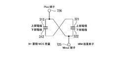
- FIG. 5 is an equivalent circuit diagram in which a P + storage type MOS capacitance element and a MIM capacitance element according to a second modification of the first embodiment are connected in parallel. It is a figure which shows for demonstrating the CV characteristic of each of the P + storage type MOS capacity element and the MIM capacity element which concerns on the 2nd modification of 1st Embodiment. It is sectional drawing in the solid-state image sensor which concerns on 3rd modification of 1st Embodiment.
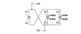
- FIG. 5 is an equivalent circuit diagram in which MIM capacitive elements according to a third modification of the first embodiment are connected in parallel.
- FIG. 5 is an equivalent circuit diagram in which a PIP capacitance element and two MIM capacitance elements according to a fourth modification of the first embodiment are connected in parallel. It is a figure which shows for demonstrating the CV characteristic of the PIP capacitance element which concerns on 4th modification of 1st Embodiment. It is sectional drawing in the solid-state image sensor which concerns on 2nd Embodiment.
- the definition of the vertical direction in the following description is merely a definition for convenience of explanation, and does not limit the technical idea of the present disclosure.
- the top and bottom are converted to left and right and read, and if the object is rotated by 180 ° and observed, the top and bottom are reversed and read.
- the effects described in the present specification are merely examples and are not limited, and other effects may be obtained.
- the solid-state image sensor 100 includes a pixel array unit 110 and peripheral circuits for reading an electric signal from the pixel array unit 110 and performing predetermined signal processing.
- the solid-state image sensor 100 uses a row selection circuit 120 for controlling row address and row scanning, a horizontal transfer scanning circuit 130 for controlling column address and column scanning, and an internal clock as a control circuit as peripheral circuits.
- the timing control circuit 140 to be generated is provided.
- the solid-state imaging device 100 according to the first embodiment includes an ADC group 150 as peripheral circuits, a digital-to-analog converter (DAC) 160 as a lamp signal generator, an amplifier circuit 170, a signal processing circuit 180, and a horizontal circuit. It has a transfer line 190.
- the solid-state image sensor 100 according to the first embodiment has a DC power supply circuit (not shown) as a peripheral circuit.
- the pixel array unit 110 is configured by arranging a large number of pixels 30 in an array shape (matrix shape).
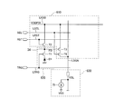
- the pixel 30 has, for example, a photoelectric conversion element D1 made of, for example, a photodiode (PD), as shown in FIG.
- the pixel 30 has four transistors, a transfer transistor T1, a reset transistor T2, an amplification transistor T3, and a selection transistor T4, as active elements with respect to the photoelectric conversion element D1.
- the constant current source load 31 is connected to the vertical signal line (LSGN) in which the pixel 30 is shared in the column direction.
- LSGN vertical signal line
- the photoelectric conversion element D1 photoelectrically converts the incident light into an electric charge (electrons in this case) in an amount corresponding to the amount of the light.
- the transfer transistor T1 as a transfer element is connected between the photoelectric conversion element D1 and the floating diffusion FD as an input node, and a transfer signal TRG which is a control signal is given to the gate (transfer gate) through the transfer control line LTRG. .. As a result, the transfer transistor T1 transfers the electrons photoelectrically converted by the photoelectric conversion element D1 to the floating diffusion FD.
- the reset transistor T2 is connected between the power supply line L VDD to which the power supply voltage VDD is supplied and the floating diffusion FD, and the reset signal RST, which is a control signal, is given to the gate through the reset control line LRST.
- the reset transistor T2 as the reset element resets the potential of the floating diffusion FD to the potential of the power supply line L VDD.
- the gate of the amplification transistor T3 as an amplification element is connected to the floating diffusion FD. That is, the floating diffusion FD functions as an input node of the amplification transistor T3 as an amplification element.
- the amplification transistor T3 and the selection transistor T4 are connected in series between the power supply line L VDD to which the power supply voltage VDD is supplied and the signal line LSGN. In this way, the amplification transistor T3 is connected to the signal line LSGN via the selection transistor T4, and constitutes a constant current source IS outside the pixel portion and a source follower.
- the selection signal SEL which is a control signal corresponding to the address signal
- the selection transistor T4 is turned on.
- the amplification transistor T3 amplifies the potential of the floating diffusion FD and outputs a voltage corresponding to the potential to the signal line LSGN.
- the voltage output from each pixel through the signal line LSGN is output to the ADC group 150. Since, for example, the gates of the transfer transistor T1, the reset transistor T2, and the selection transistor T4 are connected in row units, these operations are performed simultaneously for each pixel for one row.
- the reset control line LRST, the transfer control line LTRG, and the selection control line LSEL wired to the pixel array unit 110 are wired as a set for each row of the pixel array.
- the reset control line LRST, the transfer control line LTRG, and the selection control line LSEL are provided with M lines each.
- the reset control line LRST, the transfer control line LTRG, and the selection control line LSEL are driven by the row selection circuit 120.
- a decoupling capacitor CV1 is connected between the power supply line L VDD and ground (GND).
- the decoupling capacitor CV1 removes noise components mixed in the DC power supply voltage supplied to drive the circuit.
- the total area of the decoupling capacitor CV1 may exceed 10 mm2, and it occupies a large proportion of the chip area of the laminated CMOS image sensor.
- the comparator 151 includes a differential amplifier circuit including differential input transistors T21 and T22 forming a differential pair and active load transistors T11 and T12 including a current mirror circuit.
- the differential input transistors T21 and T22 are composed of n-type MOSFETs (hereinafter, also referred to as “nMOS”), and the active load transistors T11 and T12 are composed of p-type MOSFETs (hereinafter, also referred to as “pMOS”).
- nMOS n-type MOSFETs
- pMOS p-type MOSFETs
- the active load transistors T11 and T12 and the differential input transistors T21 and T22 serve as noise sources.
- the comparator 151 includes a reference voltage (DAC side input) Vslop, which is a ramp waveform obtained by changing the reference voltage generated by the DAC 160 in a stepwise manner, and an analog signal obtained from a pixel via the vertical signal line LSGN for each line. (VSL (Vertical Signal Line) side input) is compared.
- VSL Very Signal Line
- the counter 152 shown in FIG. 1 counts the comparison time of the comparator 151.
- the ADC group 150 has an n-bit digital signal conversion function and is arranged for each vertical signal line (column line) to form a column-parallel ADC block.
- the output of each latch 153 is connected, for example, to a horizontal transfer line 190 having a width of 2 n bits. Then, 2n amplifier circuits 170 and signal processing circuits 180 corresponding to the horizontal transfer lines 190 are arranged.
- the sampling capacitances C1 and C2 shown in FIG. 4 can be miniaturized as the capacitance density (capacity value per unit area) of the capacitance element used increases, but the bias dependence of the capacitance value is required to be small. This is because if the bias dependence of the capacitance value is large, for example, the pixel signal and the reference signal transmitted to the gate electrode of the differential input transistor of the comparator are distorted, and the accuracy of analog-to-digital conversion is significantly deteriorated. Further, a decoupling capacitor CV2 is connected to the comparator 151 between the power supply line Vdd and the ground (GND).
- FIG. 5 shows a layout diagram of each circuit constituting the solid-state image sensor 100 according to the first embodiment on a semiconductor chip.
- a metal bonding portion 230 such as a TSV (Through-silicon via). It consists of a stacked image sensor in which a part of the wiring is electrically connected.
- the pixel array unit 110 in which the pixels 30 are arranged in a matrix is mounted on the upper semiconductor substrate 210, and peripheral circuits such as the ADC group 150 and the signal processing circuit 180 other than the pixel array unit 110 are mounted on the lower semiconductor substrate 220. Will be done.
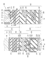
- FIG. 6 is a cross-sectional view of the solid-state image sensor 100 according to the first embodiment.
- FIG. 6A shows the outside of the pixel
- FIG. 6B shows the inside of the pixel.
- the upper semiconductor substrate 210 is composed of a photoelectric conversion layer 211, an inter-glabellar insulating film 213, and a wiring layer 214 from the top.
- the photoelectric conversion layer 211 is a layer on which a photodiode (PD) 31 is formed, and generates an electric charge according to the amount of incident light by photoelectric conversion.
- the PD 31 is electrically separated by the element separation portions 33a and 33b formed in the photoelectric conversion layer 211 for each pixel 30.
- a p-type well 32 is formed in the region in the photoelectric conversion layer 211 where the PD 31 is not formed.
- the FD34 and the n-type diffusion layer 35 are formed in the p-type well 32.
- the p-type well 32 is provided outside the pixel 30, as shown in FIG. 6A.
- the electric charge generated in the PD 31 is transferred to the FD 34 via the transfer transistor T1 provided in the glabellar insulating film 213.
- An amplification transistor T3 provided in the glabellar insulating film 213 is located near the n-type diffusion layer 35.
- Element separation portions 33b and 33c are formed at both ends of the n-type diffusion layer 35.
- the FD 34 and the pixel transistor T3 are electrically separated by the n-type diffusion layer 35 and the element separation portions 33b and 33c.
- the wiring layer 214 is configured to include wirings (M1 to M4) 215 laminated in a plurality of layers.
- the transfer transistor T1, the reset transistor T2, the amplification transistor T3, and the selection transistor T4 constituting each pixel 30 are driven via the plurality of layers of wiring (M1 to M4) 215 formed on the wiring layer 214.
- a copper (Cu) metal bonding portion 231 is provided in the wiring layer 214 to bond the metal bonding portion 231 to the lower semiconductor substrate 220.
- the lower semiconductor substrate 220 is composed of the glabella insulating film 221 and the wiring layer 222 from the top.
- the wiring layer 222 includes all wirings 223 and wirings (M1 to M6) 224 laminated in a plurality of layers.
- the inter-eyebrow insulating film 221 is provided with a copper (Cu) metal bonding portion 232 for bonding with the metal bonding portion 231 of the upper semiconductor substrate 210.
- an N + storage type MOS capacitive element 310 is arranged on the lower semiconductor substrate 220.
- the lower electrode 312 mounted on the element separating portion 311 is It is an n-type diffusion layer formed in the p-type well 228, and a gate insulating film 316 made of silicon oxide (SiO2) is placed on the lower electrode 312 thereof, and the gate insulating film 316 is placed on the gate insulating film 316.
- An upper electrode 313 made of n-type polycrystalline silicon is formed.
- This MOS capacitance element 310 is called an N + storage type MOS capacitance because electrons are accumulated on the surface of the lower electrode 312 during operation.
- the lower electrode 322 located on the side closer to the lower semiconductor substrate 220 side and the insulating film (High). (Including -K material) and a MIM (Metal Insulator Metal) capacitive element 320 formed by laminating the upper electrode 321 are mounted.
- This insulating film is any one of Ta2O2, Nb2O3, Zr02, HfO2, La2O3, Pr2O3, AL2O3, SiO2, and SiN, or a plurality of laminated films.
- the lower electrode 322 and the upper electrode 321 are a single-layer film of any one of Cu, Al, Ti, TiN, Ta, and TaN, or a plurality of laminated films.
- the wiring (M5) 224 is provided with a negative (Minus) terminal 225 and a positive (Plus) terminal 226.
- the comb-shaped wiring (MOM) capacitance element 330 shown in FIG. 8 and the PIP (Poly Insulator Poly) capacitance element 340 shown in FIG. 10 may be used.
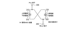
- the lower electrode 312 of the N + storage type MOS capacitance element 310 and the upper electrode 321 of the MIM capacitance element 320 are connected by a via 315 and a wiring (M6) 224, and the MOS capacitance element 310
- the MOS capacitance element 310 By connecting the upper electrode 313 and the lower electrode 322 of the MIM capacitance element 320 with the via 314 and the wiring (M5) 224, the two capacitance elements are connected in parallel.
- the first merit is that the capacitance density per unit area of the capacitive element increases. For example, if the capacitance value when the potential difference between the electrodes of the MOS capacitance element 310 is 3 V is 100 fF and the capacitance value when the potential difference between the electrodes of the MIM capacitance element 320 is 3 V is 100 fF, the two MOS capacitances are When the element 310 and the MIM capacitance element 320 are connected in parallel and operated at 3V, the capacitance value becomes 200 fF, and the capacitance density doubles.
- the TDDB can reduce the capacitance density without shortening the life as compared with the case where the film thickness of the insulating film between the electrodes of the MOS capacitive element 310 and the MIM capacitive element 320 is thinned to increase the capacitance density. Can be increased.
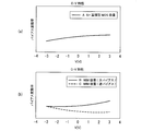
- FIG. 12A shows the CV characteristics of the N + storage type MOS capacitive element 310.
- the horizontal axis shows the potential difference between the electrodes, and the vertical axis is the value standardized by the capacitance value when the potential difference is -3V.
- the bias dependence of the capacitance value has a positive slope as shown by the solid line A.
- the CV characteristic of the MIM capacitance element 320 has a positive inclination as shown in FIG.
- the CV characteristic shows A // C in FIG. 13, and it is possible to form a capacitance element having a small voltage dependence of the capacitance value.
- FIG. 6 shows an example in which two different MOS capacitance elements 310 and MIM capacitance element 320 are arranged in the same area, but it is not always necessary to arrange them in the same area.
- the MIM capacitance element 320 having a characteristic opposite to the CV characteristic of the MOS capacitance element 310 is connected in parallel to the N + storage type MOS capacitance element 310. Therefore, the bias characteristics are canceled out, and a capacitive element having a flat bias characteristic is realized. Further, the capacitance density can be increased without shortening the life of the TDDB, as compared with the case where the film thickness of the insulating film between the electrodes of the capacitance element is thinned to increase the capacitance density.
- each capacitance element having a small bias dependence of the capacitance value and a large capacitance density without lowering the operating voltage.
- the device structure and size of each capacitance element and the connection method of each capacitance element can be optimized so that the CV characteristic of the entire capacitance element is closest to 1.
- FIG. 14 is a cross-sectional view of the solid-state image sensor 100 according to the first modification of the first embodiment.
- the same parts as those in FIG. 6A are designated by the same reference numerals, and detailed description thereof will be omitted.
- the solid-state imaging device 100 forms the MOM capacitance element 330 shown in FIG. 8 on the lower semiconductor substrate 220 by using the wirings (M1 to M4) 224, and forms them with N + storage type MOS capacitance.
- the structure is such that the element 310 and the MIM capacitance element 320 are connected in parallel.
- the upper electrode 331 of the MOM capacitance element 330 is via the lower electrode 312 of the MOS capacitance element 310, the upper electrode 321 of the MIM capacitance element 320, the via 315, and the wiring (M6) 224. Is connected.
- the lower electrode 332 of the MOM capacitance element 330 is connected to the upper electrode 313 of the MOS capacitance element 310 and the lower electrode 322 of the MIM capacitance element 320 via the via 314 and the wiring (M6) 224. With such a structure, the capacitance density can be further increased.
- the CV characteristic of the general MOM capacitance element 330 has a very small bias dependence of the capacitance value regardless of the positive or negative of the bias applied between the electrodes. In this state, it is equivalent to the CV characteristic when the N + storage type MOS capacitance element 310 and the MIM capacitance element 320 shown in FIG. 16A are connected in parallel. Therefore, even if such a MOM capacitance element 330 is added to the capacitance element in which the capacitance element 330 is connected in parallel, the bias dependence of the capacitance value of the entire capacitance element is not significantly increased. Further, since the bias dependence of the capacitance value described above does not change significantly depending on whether the bias applied between the electrodes is positive or negative, it is not necessary to be aware of the electrode connection method, and which electrode is connected to the positive (Plus) terminal 226. good.
- FIG. 17 is a cross-sectional view of the solid-state image sensor 100 according to the second modification of the first embodiment.
- the same parts as those in FIG. 6A are designated by the same reference numerals, and detailed description thereof will be omitted.
- the solid-state image sensor 100 utilizes a Hall storage type MOS capacitance element 360 (referred to as P + storage type MOS capacitance).
- the lower electrode 362 near the lower semiconductor substrate 220 side is a P-type diffusion layer formed in the n-type well 229, and silicon oxide (SiO2) is placed on the lower electrode 362.
- silicon oxide SiO2
- the upper electrode 363 of the MOS capacitive element 360 is connected to the upper electrode 321 of the MIM capacitive element 320 via the via 364 and the wiring (M6) 224.
- the lower electrode 362 of the MOS capacitance element 360 is connected to the lower electrode 322 of the MIM capacitance element 320 via the via 365 and the wiring (M6) 224.
- the CV characteristic has a negative sign of bias dependence of the capacitance value when the lower electrode 362 is fixed to 0V and the potential of the upper electrode 363 is changed by -3V to 3V. (Dotted line D).
- the bias dependence sign of the capacitance value becomes positive (solid line B). Therefore, by connecting the upper electrodes and the lower electrodes of the two capacitance elements 320 and 360 in parallel, it is possible to reduce the bias dependence of the capacitance value.
- FIG. 20 is a cross-sectional view of the solid-state image sensor 100 according to the third modification of the first embodiment.
- the same parts as those in FIG. 6A are designated by the same reference numerals, and detailed description thereof will be omitted.
- the electrodes of two MIM capacitive elements 320 and 350 formed in different layers are connected in reverse.
- the lower electrode 322 of the MIM capacitance element 320 is connected to the upper electrode 351 of the MIM capacitance element 350 via the wiring (M4) 224 and the wiring (M6) 224.
- the upper electrode 321 of the MIM capacitance element 320 is connected to the lower electrode 352 of the MIM capacitance element 350 via the wiring (M3) 224 and the wiring (M6) 224.
- the bias dependence of the capacitance value of the capacitance element in which the upper electrode 321 of the MIM capacitance element 320 and the lower electrode 352 of the MIM capacitance element 350 are connected and connected in parallel has a different sign of the bias dependence of the capacitance value in each element. Therefore, it is possible to reduce the bias dependence of the capacitance value.
- FIG. 23 is a cross-sectional view of the solid-state image sensor 100 according to the fourth modification of the first embodiment.
- the same parts as those in FIG. 6A are designated by the same reference numerals, and detailed description thereof will be omitted.
- the solid-state image sensor 100 is an example utilizing a PIP (PolyInsulatorPoly) capacitive element 340.
- the PIP capacitive element 340 is a capacitive element using polycrystalline silicon as an electrode.
- an N-type polycrystalline Si as a lower electrode 342, SiO2 as an insulating film, and N as an upper electrode.
- It is a capacitive element formed by sequentially laminating type polycrystalline Si. As a feature, the bias dependence of the capacitance value is small.
- the upper electrode 343 of the PIP capacitance element 340 is connected to the lower electrode 352 of the MIM capacitance element 350 via the wiring (M3) 224. Further, the lower electrode 342 of the PIP capacitance element 340 is connected to the upper electrode 351 of the MIM capacitance element 350 via the wiring (M4) 224.
- the MOM capacitive element 330 when applied to the first embodiment of the present disclosure, it plays the same role as the MOM capacitive element 330. That is, by adding the PIP capacitance element 340 to one of the capacitance elements connected in parallel, as shown in FIG. 25, the capacitance of the entire capacitance element does not change significantly without significantly changing the bias dependence of the capacitance value of the entire capacitance element. The value can be increased. In the case of parallel connection, either the lower electrode 342 or the upper electrode 343 may be connected to the positive side (Plus) as in the case of the MOM capacitive element 330.
- the upper electrode 313 of the MOS capacitance element 310 and the upper electrode 363 of the MOS capacitance element 360 are connected in parallel.
- the lower electrode 312 of the MOS capacitance element 310 and the lower electrode 362 of the MOS capacitance element 360 need only be connected in parallel.
- FIG. 26 is a cross-sectional view of the solid-state image sensor 100 according to the second embodiment.
- the same parts as those in FIG. 14 are designated by the same reference numerals, and detailed description thereof will be omitted.
- the capacitance element is mounted on both chips of the upper semiconductor substrate 210 and the lower semiconductor substrate 220, and the upper semiconductor substrate 210 is used by using the metal bonding portion 230 arranged on the bonding surface.
- the capacitive elements mounted on the lower semiconductor substrate 220 are connected in parallel.
- the upper semiconductor substrate 210 is composed of a p-type well 32, an inter-glabellar insulating film 213, and a wiring layer 214 from the top.
- An N + storage type MOS capacitive element 410 is arranged below the upper semiconductor substrate 210. Assuming that the electrode closer to the lower semiconductor substrate 220 side on which the MOS capacitance element 410 is mounted is the lower electrode 412, the lower electrode 412 is an n-type diffusion layer formed in the p-type well 32.
- a gate insulating film 416 made of silicon oxide (SiO2) is placed on the lower electrode 412, and an upper electrode 413 made of n-type polycrystalline silicon is formed on the gate insulating film 416.
- the wiring (M1 to M4) 215 is used in the MOM.
- a capacitive element 420 is formed.
- the upper electrode 421 of the MOM capacitance element 420 is connected to the upper electrode 413 of the MOS capacitance element 410 via the via 414.
- the lower electrode 422 of the MOM capacitance element 420 is connected to the lower electrode 412 of the MOS capacitance element 410 via the via 415.
- the upper electrode 413 of the MOS capacitance element 410 and the upper electrode 421 of the MOM capacitance element 420 are connected to the upper electrode of the MOS capacitance element 310 on the lower semiconductor substrate 220 side via the copper (Cu) metal coupling portions 231 and 232.
- the 313, the lower electrode 322 of the MIM capacitance element 320, and the upper electrode 331 of the MOM capacitance element 330 are connected.
- the lower electrode 412 of the MOS capacitance element 410 and the lower electrode 422 of the MOM capacitance element 420 are connected to the lower electrode of the MOS capacitance element 310 on the lower semiconductor substrate 220 side via the copper (Cu) metal coupling portions 231 and 232.
- the 312, the upper electrode 321 of the MIM capacitance element 320, and the lower electrode 332 of the MOM capacitance element 330 are connected.
- the bias-dependent code of the capacitance value of each capacitive element is N + accumulation.
- the type MOS capacitance elements 310 and 410 are positive, and the MIM capacitance element 320 is negative.
- the N + storage type MOS capacitance elements 310 and 410 and the MIM capacitance element 320 have opposite bias-dependent inclination signs, so optimize these element sizes. For example, it is possible to make the bias dependence of the capacitance value of the entire capacitance element formed by connecting these in parallel very small.
- the capacitance values of the MOS capacitance element 410 and the MOM capacitance element 420 of the upper semiconductor substrate 210 (sensor unit) can be added as compared with the first embodiment.
- the N + storage type MOS capacitance element 310 and the N + storage type MOS capacitance element 410 are 100 fF
- the capacitance values of the MOM capacitance element 330 and the MOM capacitance element 420 are 30 fF
- the MIM capacitance element 320 is 100 fF.
- the total capacitance value of the parallel capacitance element is 3.6 times the capacitance value of the N + storage type MOS capacitance element 310 alone.
- FIG. 28 is a cross-sectional view of the solid-state image sensor 100 according to the first modification of the second embodiment.
- the same parts as those in FIG. 26 are designated by the same reference numerals, and detailed description thereof will be omitted.
- the solid-state imaging device 100 mounts the same N + storage type MOS capacitance element 310 and MOM capacitance element 330 as in the first embodiment on the lower semiconductor substrate 220 (peripheral circuit portion), and mounts the upper semiconductor substrate.
- the 210 sensor unit
- the 210 is equipped with a P + storage type MOS capacitance element 430 and a MOM capacitance element 420.
- the MOS capacitive element 430 the lower electrode 431 near the upper semiconductor substrate 210 side is a P-type diffusion layer, and a gate insulating film 436 made of silicon oxide (SiO2) is provided on the lower electrode 431.
- An upper electrode 432 made of P-type polycrystalline silicon is formed on the gate insulating film 436.
- the upper electrode 421 of the MOM capacitance element 420 is connected to the upper electrode 432 of the MOS capacitance element 430 via the via 414. Further, the lower electrode 422 of the MOM capacitance element 420 is connected to the lower electrode 431 of the MOS capacitance element 430 via the via 415.
- the upper electrode 432 of the MOS capacitance element 430 and the upper electrode 421 of the MOM capacitance element 420 are connected to the upper electrode of the MOS capacitance element 310 on the lower semiconductor substrate 220 side via the copper (Cu) metal coupling portions 231 and 232.
- the 313 is connected to the upper electrode 331 of the MOM capacitive element 330.
- the lower electrode 431 of the MOS capacitance element 430 and the lower electrode 422 of the MOM capacitance element 420 are the lower electrodes of the MOS capacitance element 310 on the lower semiconductor substrate 220 side via the metal coupling portions 231 and 232 made of copper (Cu).
- the 312 is connected to the lower electrode 332 of the MOM capacitive element 330.
- FIG. 30 is a cross-sectional view of the solid-state image sensor 100 according to the second modification of the second embodiment.
- the same parts as those in FIG. 30 are designated by the same reference numerals, and detailed description thereof will be omitted.
- the solid-state imaging device 100 functions as a capacitive element by facing the metal bonding portion 511 on the upper semiconductor substrate 210 side and the metal bonding portion 512 on the lower semiconductor substrate 220 side arranged on the bonding surface. Is connected in parallel with other capacitance elements to further increase the capacitance density.
- This capacitive element is called a junction capacitive element 510.
- the metal bonding portion 511 on the upper semiconductor substrate 210 side is used as the upper electrode
- the metal bonding portion 512 on the lower semiconductor substrate 220 side is used as the lower electrode.
- the upper electrode (metal bonding portion 511) of the junction capacitance element 510 is connected to the upper electrode 413 of the MOS capacitance element 410, the upper electrode 421 of the MOM capacitance element 420, and via via 414.
- the lower electrode (metal bonding portion 512) of the junction capacitance element 510 is connected to the lower electrode 412 of the MOS capacitance element 410 and the lower electrode 422 of the MOM capacitance element 420 via the via 415.
- the upper electrode (metal coupling portion 511) of the junction capacitance element 510 includes the upper electrode 313 of the MOS capacitance element 310 on the lower semiconductor substrate 220 side, the lower electrode 322 of the MIM capacitance element 320, and the MOM capacitance element 330. It is connected to the upper electrode 331.
- the lower electrode (metal coupling portion 512) of the junction capacitance element 510 includes the lower electrode 312 of the MOS capacitance element 310 on the lower semiconductor substrate 220 side, the upper electrode 321 of the MIM capacitance element 320, and the MOM capacitance element 330. It is connected to the lower electrode 332.
- the junction capacitance element 510 has the function of a capacitance element by facing metal materials, and the bias dependence of the capacitance value is very small like the MOM capacitance elements 330 and 420. Therefore, by connecting the junction capacitance elements 510 in parallel, the bias dependence of the capacitance value of the connection source capacitance element does not change significantly, and the capacitance density increases.
- the metal coupling portions 511 and 512 of the upper semiconductor substrate 210 and the lower semiconductor substrate 220 are formed as the junction capacitance element 510, thereby forming the capacitance element.
- the overall capacity value can be increased.
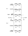
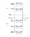
- FIG. 32 is a table showing capacitive elements that can be mounted on the upper semiconductor substrate 210 (Chip1) and the lower semiconductor substrate 220 (Chip2) by using a general CMOS process.
- connection direction of the electrodes of the table in FIG. 32 is "positive" when the upper electrode of each capacitance element is connected to the Plus terminal and the lower electrode is connected to the negative (Minus) terminal 225.
- the case where the upper electrode of each capacitance element is connected to the negative (Minus) terminal 225 and the lower electrode is connected to the positive (Plus) terminal 226 is “reverse”. Elements that have a very small bias dependence of the capacitance value and that can be connected to either terminal without any problem are described as "no matter”.
- the sign of the bias-dependent slope of the capacitance value is that the negative (Minus) terminal 225 is described as 0V and the positive (Plus) terminal 226 is changed by -3 to 3V in the connection described in the electrode connection direction. It is a bias-dependent code of the capacitance value at the time. From the table of FIG. 32, in a laminated structure in which two chips are laminated, a plurality of capacitive elements can be connected in parallel by a desired connection method to achieve both the capacitance density set in Target and the bias dependence of the capacitance value. There are numerous combinations. Although not all combinations thereof can be described in the embodiment, the designer makes an optimum selection in consideration of the characteristics required for the circuit to be designed, the available Chip area, and the manufacturing cost for mounting each element. Just do.
- a photoelectric conversion element and an amplification transistor for amplifying a signal from the photoelectric conversion element are arranged on different substrates, and a sensor unit in which the photoelectric conversion element and the transfer gate (TRG) are arranged and amplification are provided.
- TRG transfer gate
- a solid-state imaging device in which three substrates on which a pixel transistor portion in which a pixel transistor such as a transistor is arranged and a peripheral circuit portion in which a signal processing circuit for processing a signal from an amplification transistor is arranged are laminated by WoW technology will be described.
- FIG. 33 is a cross-sectional view of the solid-state image sensor 100A according to the third embodiment.
- FIG. 33 (a) shows the outside of the pixel
- FIG. 33 (b) shows the inside of the pixel.
- the same parts as those in FIG. 26 are designated by the same reference numerals, and detailed description thereof will be omitted.
- the solid-state image sensor 100A is composed of a sensor unit 610, a pixel transistor unit 620, and a peripheral circuit unit 630 from the top.
- a sensor unit 610 In the solid-state image sensor 100A, three semiconductor chips of a sensor unit 610, a pixel transistor unit 620, and a peripheral circuit unit 630 are superposed, and a part of the wiring is electrically connected by a metal coupling unit 640. It is composed of stacked image sensors that are connected to each other.
- the transfer transistor T1, the photoelectric conversion element D1, and the floating diffusion FD34 are arranged in the sensor unit 610.
- a reset transistor T2, an amplification transistor T3, and a selection transistor T4 are arranged in the pixel transistor section 620.
- the sensor unit 610 is composed of the photoelectric conversion layer 611 and the glabella insulating film 612 from above.
- the photoelectric conversion layer 211 is a layer on which a photodiode (PD) 31 is formed, and generates an electric charge according to the amount of incident light by photoelectric conversion.
- the PD 31 is electrically separated by element separation portions 33a and 33b formed in the photoelectric conversion layer 611 for each pixel 30.
- the FD34 and the gate electrode 36 of the transfer transistor T1 are formed on the photoelectric conversion layer 611.
- a transfer transistor T1 is formed on the glabellar insulating film 612.
- the pixel transistor section 620 is composed of a p-type well 621 and a wiring layer 622 from the top. An n-type diffusion layer is formed in the p-type well 621.
- the wiring layer 622 includes wirings (M1 to M4) 623 laminated in a plurality of layers.
- the transfer transistor T1, the reset transistor T2, the amplification transistor T3, and the selection transistor T4 constituting each pixel 30 are driven via the plurality of layers of wiring (M1 to M4) 623 formed on the wiring layer 622. Further, a copper (Cu) metal bonding portion 641 is provided in the wiring layer 622 to join the peripheral circuit portion 630.
- Cu copper
- the peripheral circuit unit 630 is composed of an inter-glabellar insulating film and a wiring layer from above.
- the wiring layer includes all wirings 631 and wirings (M1 to M6) 632 laminated on a plurality of layers.
- the glabellar insulating film is provided with a copper (Cu) metal bonding portion 642 for bonding with the metal bonding portion 641 of the pixel transistor portion 620.
- the generated charge is a pixel signal on the signal line LSGN shown in FIG. 1 formed by the wiring (M1 to M4) 623 and the wiring (M1 to M6) 632 of the peripheral circuit unit 630 via the amplification transistor T3. Is output to the ADC group 150 formed in the peripheral circuit unit 630.
- an N + storage type MOS capacitive element 310 is arranged on the peripheral circuit unit 630.
- the MOM capacitance element 330 and the MIM capacitance element 320 are arranged on the upper layer of the MOS capacitance element 310.
- An N + storage type MOS capacitive element 410 is arranged below the pixel transistor section 620.
- the wiring (M1 to M4) 623 is used for MOM.
- a capacitive element 420 is formed.
- the upper electrode 421 of the MOM capacitance element 420 is connected to the upper electrode 413 of the MOS capacitance element 410 via the via 414.
- the lower electrode 422 of the MOM capacitance element 420 is connected to the lower electrode 412 of the MOS capacitance element 410 via the via 415.
- the upper electrode 413 of the MOS capacitance element 410 and the upper electrode 421 of the MOM capacitance element 420 are connected to the upper electrode 313 of the MOS capacitance element 310 on the peripheral circuit portion 630 side via the copper (Cu) metal coupling portions 641 and 642.
- the lower electrode 322 of the MIM capacitance element 320 and the upper electrode 331 of the MOM capacitance element 330 are connected.
- the lower electrode 412 of the MOS capacitance element 410 and the lower electrode 422 of the MOM capacitance element 420 are connected to the lower electrode 312 of the MOS capacitance element 310 on the peripheral circuit portion 630 side via the copper (Cu) metal coupling portions 641 and 642.
- the upper electrode 321 of the MIM capacitance element 320 and the lower electrode 332 of the MOM capacitance element 330 are connected.
- the negative (Minus) terminal 225 is fixed to 0V
- the positive (Plus) terminal 226 is set to -3 to -3 to 3.
- the bias-dependent codes of the capacitance values of the respective capacitance elements when changed by 3 V are the N + storage type MOS capacitance element 310 and the N + storage type MOS capacitance element 410. It is positive and the MIM capacitive element 320 becomes negative.
- the N + storage type MOS capacitance element 310 and the N + storage type MOS capacitance element 410 and the MIM capacitance element 320 have opposite bias-dependent inclination signs.
- the three-layer laminated image sensor can also be equipped with a capacitance element having a large capacitance value and a small bias dependence of the capacitance value.
- a fourth embodiment of the present disclosure describes a solid-state image sensor applied to a photodetector using a SPAD (Single Photon Avalanche Diode).
- FIG. 37 shows a layout diagram of each circuit constituting the solid-state image sensor 100B according to the fourth embodiment on the semiconductor chip.
- a metal bonding portion 730 such as a TSV (Through-silicon via). It consists of a stacked image sensor in which a part of the wiring is electrically connected.
- the SPAD photodiodes 41 are arranged in a matrix on the upper semiconductor substrate 710, and peripheral circuits 51 such as the ADC group 150 and the signal processing circuit 180 other than the SPAD photodiode 41 are mounted on the lower semiconductor substrate 720.
- FIG. 38 is a cross-sectional view of the solid-state image sensor 100B according to the fourth embodiment.
- FIG. 38 (a) shows the outside of the pixel
- FIG. 38 (b) shows the inside of the pixel.
- the upper semiconductor substrate 710 is composed of a photoelectric conversion layer 711, an inter-glabellar insulating film 713, and a wiring layer 714 from the top.
- the photoelectric conversion layer 711 is a layer on which a SPAD photodiode 41 is formed, detects incident light (photons), and converts carriers generated thereby into electrical signal pulses using avalanche multiplier.
- the SPAD photodiode 41 is electrically separated by a p-type diffusion layer 42a and an n-type diffusion layer 42b formed in the photoelectric conversion layer 711 for each pixel 30.
- a p-type diffusion layer 42a is electrically separated by a p-type diffusion layer 42a and an n-type diffusion layer 42b formed in the photoelectric conversion layer 711 for each pixel 30.
- p-type well 43 is provided outside the pixel 30, as shown in FIG. 38 (a).
- the electric signal pulse generated from the SPAD photodiode 41 is output to the wiring (M1 to M4) 715 formed in the wiring layer 714 via the via 716 formed in the inter-glabella insulating film 713.
- a copper (Cu) metal bonding portion 731 is provided in the wiring layer 714 to bond the metal bonding portion 731 to the lower semiconductor substrate 720.
- the lower semiconductor substrate 720 is composed of the glabella insulating film 721 and the wiring layer 722 from the top.
- the wiring layer 722 includes all wirings 723 and wirings (M1 to M6) 724 laminated in a plurality of layers.
- the inter-eyebrow insulating film 721 is provided with a copper (Cu) metal bonding portion 732 for bonding with the metal bonding portion 731 of the upper semiconductor substrate 710.
- the light detected by the upper semiconductor substrate 210 is photoelectrically converted by the SPAD photodiode 41 to generate an electric signal pulse. Then, the electric signal pulse is output to the peripheral circuit 51 via the signal line LSGN shown in FIG. 1 formed by the wiring (M1 to M4) 715 and the wiring (M1 to M6) 724 of the lower semiconductor substrate 720. ..
- an N + storage type MOS capacitive element 310 is arranged on the lower semiconductor substrate 720.
- the lower electrode 322 located on the side closer to the lower semiconductor substrate 220 side and the insulating film (High). (Including -K material) and a MIM (Metal Insulator Metal) capacitive element 320 formed by laminating the upper electrode 321 are mounted.
- the lower electrode 312 of the N + storage type MOS capacitance element 310 and the upper electrode 321 of the MIM capacitance element 320 are connected by a via 315 and a wiring (M6) 724, and the MOS capacitance element 310
- the MOS capacitance element 310 By connecting the upper electrode 313 and the lower electrode 322 of the MIM capacitance element 320 with the via 314 and the wiring (M5) 724, the two capacitance elements are connected in parallel.
- the semiconductor device according to the present technology can be applied to a capacitor constituting a general filter circuit.
- a general filter circuit includes a resistor R11 and a capacitor C11, and a semiconductor device according to the present technology can be applied as a configuration of the capacitor C11.
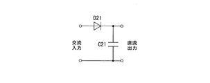
- a general filter circuit includes a diode D21 and a capacitor C21, and a semiconductor device according to the present technology can be applied as a configuration of the capacitor C21.
- a general integral circuit includes a resistor R32, a capacitor C31, and an operational amplifier 800, and a semiconductor device according to the present technology can be applied as a configuration of the capacitor C31.
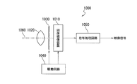
- FIG. 43 is a schematic configuration diagram of the electronic device 1000 according to the sixth embodiment of the present disclosure.
- the electronic device 1000 according to the sixth embodiment includes a solid-state imaging device 1010, an optical lens 1020, a shutter device 1030, a drive circuit 1040, and a signal processing circuit 1050.
- the electronic device 1000 of the sixth embodiment shows an embodiment in which the solid-state image sensor 100 according to the first embodiment of the present disclosure is used as an electronic device (for example, a camera) as the solid-state image sensor 1010.
- the optical lens 1020 forms an image of image light (incident light 1060) from the subject on the image pickup surface of the solid-state image pickup device 1010. As a result, the signal charge is accumulated in the solid-state image sensor 1010 for a certain period of time.
- the shutter device 1030 controls the light irradiation period and the light blocking period of the solid-state image sensor 1010.
- the drive circuit 1040 supplies a drive signal for controlling the transfer operation of the solid-state image sensor 1010 and the shutter operation of the shutter device 1030.
- the signal transfer of the solid-state image sensor 1010 is performed by the drive signal (timing signal) supplied from the drive circuit 1040.
- the signal processing circuit 1050 performs various signal processing on the signal (pixel signal) output from the solid-state imaging device 1010.
- the video signal after signal processing is stored in a storage medium such as a memory or output to a monitor.
- the optical color mixing is suppressed in the solid-state image sensor 1010, so that the image quality of the video signal can be improved.
- the electronic device 1000 to which the solid-state image sensors 100, 100A, and 100B can be applied is not limited to the camera, but can be applied to other electronic devices. For example, it may be applied to an imaging device such as a camera module for mobile devices such as mobile phones.
- the solid-state image sensors 100, 100A, and 100B according to the first to fourth embodiments are used for the electronic device, but other configurations may be used.
- the present disclosure may also have the following structure.
- (1) With a semiconductor substrate The first capacitive element laminated on the semiconductor substrate and It is provided with a second capacitive element that is laminated on the side of the first capacitive element opposite to the semiconductor substrate side and has a characteristic opposite to the bias characteristic of the capacitance value of the first capacitive element.
- the first capacitive element and the second capacitive element are semiconductor devices connected in parallel.
- (2) The first and second capacitive elements are provided with n (n is an integer).
- the capacitance value of the entire element when the potential difference between the electrodes is the operating voltage is set to Capital (V)
- the capacitance value of the entire element when the potential difference between the electrodes is 0 is set to Total (0), and each capacitance is set.
- the semiconductor device is a first conductive type storage type MOS capacitive element having a lower electrode formed on the semiconductor substrate side and an upper electrode facing the lower electrode with an insulating film interposed therebetween.
- the second capacitive element has a lower electrode formed on the semiconductor substrate side and an upper electrode facing the lower electrode with an insulating film interposed therebetween, and has the opposite polarity to that of the first conductive type.
- the second conductive type storage type MOS capacitance element of The upper electrode of the first conductive type storage type MOS capacitance element is connected to the upper electrode of the second conductive type storage type MOS capacitance element, and the lower electrode of the first conductive type storage type MOS capacitance element is connected.
- the first capacitive element is a first conductive type storage type MOS capacitive element having a lower electrode formed on the semiconductor substrate side and an upper electrode facing the lower electrode with an insulating film interposed therebetween.
- the second capacitive element is a MIM (Metal Insulator Metal) capacitive element having a lower electrode formed on the semiconductor substrate side and an upper electrode facing the lower electrode with an insulating film interposed therebetween.
- the upper electrode of the first conductive type storage type MOS capacitance element and the lower electrode of the MIM capacitance element are connected, and the lower electrode of the first conductive type storage type MOS capacitance element and the upper part of the MIM capacitance element are connected.
- the semiconductor device which includes a parallel connection structure for connecting electrodes.
- the first capacitive element has a lower electrode formed on the semiconductor substrate side and an upper electrode facing the lower electrode with an insulating film interposed therebetween, and has a polarity opposite to that of the first conductive type. It is a second conductive type storage type MOS capacitance element.
- the second capacitive element is a MIM capacitive element having a lower electrode formed on the semiconductor substrate side and an upper electrode facing the lower electrode with an insulating film interposed therebetween.
- the upper electrode of the second conductive type storage type MOS capacity element and the upper electrode of the MIM capacity element are connected, and the lower electrode of the second conductive type storage type MOS capacity element and the lower part of the MIM capacity element are connected.
- the first capacitive element is a first MIM capacitive element having a lower electrode formed on the semiconductor substrate side and an upper electrode facing the lower electrode with an insulating film interposed therebetween.
- the second capacitive element is a second MIM capacitive element having a lower electrode formed on the semiconductor substrate side and an upper electrode facing the lower electrode with an insulating film interposed therebetween.
- the semiconductor device according to (1) or (2) above which includes a parallel connection structure for connecting the above.
- the semiconductor device according to any one of (1) to (6) above which includes a structure in which comb-shaped wiring capacitance elements are connected in parallel.
- the semiconductor device according to any one of (1) to (7) above further comprising a structure in which PIP (Poly Insulator Poly) type capacitive elements are connected in parallel.
- Another semiconductor substrate having a third capacitive element is provided.
- the other semiconductor substrate is bonded to the semiconductor substrate, and the bias characteristic of the capacitance value of the entire capacitance element of the first capacitance element, the second capacitance element, and the third capacitance element is closest to 1.
- the semiconductor device according to (9) above which includes a structure in which a junction between the semiconductor substrate and the other semiconductor substrate is a capacitive element.
- the semiconductor substrate has at least one of a pixel and a peripheral circuit that processes a signal from a pixel transistor that amplifies the signal from the pixel.
- the pixel consists of a photodiode
- the semiconductor substrate having the peripheral circuit includes a first semiconductor substrate having the pixel transistor and a second semiconductor substrate having the peripheral circuit.
- the semiconductor substrate has at least one of a sensor unit having a SPAD (Single Photon Avalanche Diode) photodiode and a peripheral circuit for processing a signal from the sensor unit.
- SPAD Single Photon Avalanche Diode
- the first capacitive element laminated on the semiconductor substrate and The first capacitive element is laminated on the side opposite to the semiconductor substrate side, and includes a second capacitive element having a characteristic opposite to the bias characteristic of the capacitance value of the first capacitive element.
- the first capacitive element and the second capacitive element are provided with a semiconductor device connected in parallel. Electronics.
- Horizontal transfer line 210, 710 ... Upper semiconductor substrate, 211, 611, 711 ... Photoelectric conversion layer, 213,221,612,713,721 ... Intereural insulating film, 215,223,224,623,631,632,715,723,724 ... Wiring, 214,222,622,714, 722 ... Wiring layer, 220, 720 ... Lower semiconductor substrate, 225 ... Negative terminal, 226 ... Positive terminal, 230, 231,232, 511, 512,640, 641, 642,730, 731, 732 ... Metal joint, 310, 360 ... MOS capacitive element, 312,322,332 ... lower electrode, 313,321,331 ... upper electrode, 314,315,716 ...
Landscapes
- Engineering & Computer Science (AREA)
- Multimedia (AREA)
- Signal Processing (AREA)
- Solid State Image Pick-Up Elements (AREA)
- Semiconductor Integrated Circuits (AREA)
Priority Applications (4)
| Application Number | Priority Date | Filing Date | Title |
|---|---|---|---|
| US17/910,915 US12170303B2 (en) | 2020-03-30 | 2021-02-17 | Semiconductor device and electronic equipment |
| JP2022511644A JP7645240B2 (ja) | 2020-03-30 | 2021-02-17 | 半導体装置及び電子機器 |
| DE112021002165.6T DE112021002165T5 (de) | 2020-03-30 | 2021-02-17 | Halbleitervorrichtung und elektronische ausrüstung |
| CN202180023374.3A CN115315807A (zh) | 2020-03-30 | 2021-02-17 | 半导体装置及电子设备 |
Applications Claiming Priority (2)
| Application Number | Priority Date | Filing Date | Title |
|---|---|---|---|
| JP2020060404 | 2020-03-30 | ||
| JP2020-060404 | 2020-03-30 |
Publications (1)
| Publication Number | Publication Date |
|---|---|
| WO2021199754A1 true WO2021199754A1 (ja) | 2021-10-07 |
Family
ID=77929698
Family Applications (1)
| Application Number | Title | Priority Date | Filing Date |
|---|---|---|---|
| PCT/JP2021/005876 Ceased WO2021199754A1 (ja) | 2020-03-30 | 2021-02-17 | 半導体装置及び電子機器 |
Country Status (5)
| Country | Link |
|---|---|
| US (1) | US12170303B2 (https=) |
| JP (1) | JP7645240B2 (https=) |
| CN (1) | CN115315807A (https=) |
| DE (1) | DE112021002165T5 (https=) |
| WO (1) | WO2021199754A1 (https=) |
Cited By (1)
| Publication number | Priority date | Publication date | Assignee | Title |
|---|---|---|---|---|
| US11735616B2 (en) * | 2021-12-29 | 2023-08-22 | Nanya Technology Corporation | Optical semiconductor device with integrated dies |
Citations (5)
| Publication number | Priority date | Publication date | Assignee | Title |
|---|---|---|---|---|
| JPH04241449A (ja) * | 1991-01-16 | 1992-08-28 | Hitachi Ltd | 半導体集積回路装置 |
| JP2006128468A (ja) * | 2004-10-29 | 2006-05-18 | Seiko Epson Corp | 半導体装置 |
| JP2007208101A (ja) * | 2006-02-03 | 2007-08-16 | Toshiba Corp | 半導体装置 |
| JP2013143446A (ja) * | 2012-01-10 | 2013-07-22 | Sony Corp | 容量素子、半導体装置及び電子機器 |
| JP2016511941A (ja) * | 2013-02-19 | 2016-04-21 | クアルコム,インコーポレイテッド | 相補型バックエンドオブライン(beol)キャパシタ |
Family Cites Families (7)
| Publication number | Priority date | Publication date | Assignee | Title |
|---|---|---|---|---|
| JP4371799B2 (ja) | 2003-12-19 | 2009-11-25 | 株式会社リコー | 容量素子 |
| JP5512609B2 (ja) | 2011-07-11 | 2014-06-04 | ルネサスエレクトロニクス株式会社 | 半導体集積回路装置 |
| US10264199B2 (en) * | 2014-07-15 | 2019-04-16 | Brillnics Inc. | Solid-state imaging device, method for producing solid-state imaging device, and electronic apparatus using photoelectric conversion elements |
| JP2018037626A (ja) | 2016-09-02 | 2018-03-08 | 旭化成エレクトロニクス株式会社 | 半導体装置及び半導体装置の製造方法 |
| JP2018088648A (ja) | 2016-11-29 | 2018-06-07 | ルネサスエレクトロニクス株式会社 | 固体撮像装置 |
| JP2018148528A (ja) | 2017-03-09 | 2018-09-20 | ソニーセミコンダクタソリューションズ株式会社 | 固体撮像装置および電子機器 |
| WO2019063892A1 (fr) * | 2017-09-27 | 2019-04-04 | Airbus Defence And Space Sas | Redimensionnement des entites de detection d'un capteur d'image matriciel hybride |
-
2021
- 2021-02-17 JP JP2022511644A patent/JP7645240B2/ja active Active
- 2021-02-17 CN CN202180023374.3A patent/CN115315807A/zh active Pending
- 2021-02-17 US US17/910,915 patent/US12170303B2/en active Active
- 2021-02-17 WO PCT/JP2021/005876 patent/WO2021199754A1/ja not_active Ceased
- 2021-02-17 DE DE112021002165.6T patent/DE112021002165T5/de active Pending
Patent Citations (5)
| Publication number | Priority date | Publication date | Assignee | Title |
|---|---|---|---|---|
| JPH04241449A (ja) * | 1991-01-16 | 1992-08-28 | Hitachi Ltd | 半導体集積回路装置 |
| JP2006128468A (ja) * | 2004-10-29 | 2006-05-18 | Seiko Epson Corp | 半導体装置 |
| JP2007208101A (ja) * | 2006-02-03 | 2007-08-16 | Toshiba Corp | 半導体装置 |
| JP2013143446A (ja) * | 2012-01-10 | 2013-07-22 | Sony Corp | 容量素子、半導体装置及び電子機器 |
| JP2016511941A (ja) * | 2013-02-19 | 2016-04-21 | クアルコム,インコーポレイテッド | 相補型バックエンドオブライン(beol)キャパシタ |
Cited By (1)
| Publication number | Priority date | Publication date | Assignee | Title |
|---|---|---|---|---|
| US11735616B2 (en) * | 2021-12-29 | 2023-08-22 | Nanya Technology Corporation | Optical semiconductor device with integrated dies |
Also Published As
| Publication number | Publication date |
|---|---|
| US20230207597A1 (en) | 2023-06-29 |
| JPWO2021199754A1 (https=) | 2021-10-07 |
| DE112021002165T5 (de) | 2023-03-23 |
| JP7645240B2 (ja) | 2025-03-13 |
| US12170303B2 (en) | 2024-12-17 |
| CN115315807A (zh) | 2022-11-08 |
Similar Documents
| Publication | Publication Date | Title |
|---|---|---|
| US12149853B2 (en) | Photoelectric conversion device, electronic device, and substrate | |
| US10554912B2 (en) | Semiconductor apparatus, solid-state image sensing apparatus, and camera system | |
| US9661246B2 (en) | Solid state image pickup device having a capacitor structure made up of a plurality of capacitors | |
| KR20160040139A (ko) | 촬상 장치, 전자 기기 | |
| US20250357942A1 (en) | Image sensor and image capturing device | |
| JP7645240B2 (ja) | 半導体装置及び電子機器 | |
| WO2022249638A1 (ja) | 撮像素子及び撮像装置 | |
| JP7695932B2 (ja) | 半導体装置及び電子機器 | |
| WO2021033454A1 (ja) | 半導体装置及び電子機器 | |
| US20250317669A1 (en) | Image sensor and semiconductor device including capacitor structure |
Legal Events
| Date | Code | Title | Description |
|---|---|---|---|
| 121 | Ep: the epo has been informed by wipo that ep was designated in this application |
Ref document number: 21779236 Country of ref document: EP Kind code of ref document: A1 |
|
| ENP | Entry into the national phase |
Ref document number: 2022511644 Country of ref document: JP Kind code of ref document: A |
|
| 122 | Ep: pct application non-entry in european phase |
Ref document number: 21779236 Country of ref document: EP Kind code of ref document: A1 |
|
| 122 | Ep: pct application non-entry in european phase |
Ref document number: 21779236 Country of ref document: EP Kind code of ref document: A1 |