WO2021199754A1 - Semiconductor device and electronic apparatus - Google Patents
Semiconductor device and electronic apparatus Download PDFInfo
- Publication number
- WO2021199754A1 WO2021199754A1 PCT/JP2021/005876 JP2021005876W WO2021199754A1 WO 2021199754 A1 WO2021199754 A1 WO 2021199754A1 JP 2021005876 W JP2021005876 W JP 2021005876W WO 2021199754 A1 WO2021199754 A1 WO 2021199754A1
- Authority
- WO
- WIPO (PCT)
- Prior art keywords
- capacitance
- semiconductor substrate
- capacitive element
- lower electrode
- capacitance element
- Prior art date
Links
- 239000004065 semiconductor Substances 0.000 title claims abstract description 178
- 239000000758 substrate Substances 0.000 claims abstract description 127
- 238000003860 storage Methods 0.000 claims description 64
- 239000002184 metal Substances 0.000 claims description 41
- 229910052751 metal Inorganic materials 0.000 claims description 41
- 230000002093 peripheral effect Effects 0.000 claims description 39
- 238000000034 method Methods 0.000 claims description 18
- 230000008569 process Effects 0.000 claims description 12
- 239000012212 insulator Substances 0.000 claims description 8
- 239000010410 layer Substances 0.000 description 62
- 230000004048 modification Effects 0.000 description 32
- 238000012986 modification Methods 0.000 description 32
- 238000006243 chemical reaction Methods 0.000 description 30
- 239000010949 copper Substances 0.000 description 25
- 238000010586 diagram Methods 0.000 description 22
- 238000009792 diffusion process Methods 0.000 description 21
- 238000005516 engineering process Methods 0.000 description 19
- 230000003321 amplification Effects 0.000 description 17
- 239000003990 capacitor Substances 0.000 description 17
- 238000003199 nucleic acid amplification method Methods 0.000 description 17
- 229910052802 copper Inorganic materials 0.000 description 13
- RYGMFSIKBFXOCR-UHFFFAOYSA-N Copper Chemical compound [Cu] RYGMFSIKBFXOCR-UHFFFAOYSA-N 0.000 description 12
- 230000008878 coupling Effects 0.000 description 12
- 238000010168 coupling process Methods 0.000 description 12
- 238000005859 coupling reaction Methods 0.000 description 12
- VYPSYNLAJGMNEJ-UHFFFAOYSA-N Silicium dioxide Chemical compound O=[Si]=O VYPSYNLAJGMNEJ-UHFFFAOYSA-N 0.000 description 10
- 229910052814 silicon oxide Inorganic materials 0.000 description 10
- 230000000694 effects Effects 0.000 description 9
- 238000003384 imaging method Methods 0.000 description 9
- 230000001419 dependent effect Effects 0.000 description 8
- 238000007667 floating Methods 0.000 description 8
- 229910021420 polycrystalline silicon Inorganic materials 0.000 description 7
- 230000009471 action Effects 0.000 description 6
- 230000008859 change Effects 0.000 description 5
- 230000006870 function Effects 0.000 description 5
- 101001018097 Homo sapiens L-selectin Proteins 0.000 description 4
- 102100033467 L-selectin Human genes 0.000 description 4
- 238000004519 manufacturing process Methods 0.000 description 4
- 230000003287 optical effect Effects 0.000 description 4
- 238000000926 separation method Methods 0.000 description 4
- 238000010030 laminating Methods 0.000 description 3
- 239000011159 matrix material Substances 0.000 description 3
- 238000009825 accumulation Methods 0.000 description 2
- 238000009499 grossing Methods 0.000 description 2
- 239000000463 material Substances 0.000 description 2
- 238000005070 sampling Methods 0.000 description 2
- 238000004904 shortening Methods 0.000 description 2
- 229910052710 silicon Inorganic materials 0.000 description 2
- 239000010703 silicon Substances 0.000 description 2
- 235000012431 wafers Nutrition 0.000 description 2
- 229910019714 Nb2O3 Inorganic materials 0.000 description 1
- ATJFFYVFTNAWJD-UHFFFAOYSA-N Tin Chemical compound [Sn] ATJFFYVFTNAWJD-UHFFFAOYSA-N 0.000 description 1
- MCMNRKCIXSYSNV-UHFFFAOYSA-N ZrO2 Inorganic materials O=[Zr]=O MCMNRKCIXSYSNV-UHFFFAOYSA-N 0.000 description 1
- 230000000903 blocking effect Effects 0.000 description 1
- 239000000969 carrier Substances 0.000 description 1
- 230000015556 catabolic process Effects 0.000 description 1
- 230000000295 complement effect Effects 0.000 description 1
- 238000005520 cutting process Methods 0.000 description 1
- CJNBYAVZURUTKZ-UHFFFAOYSA-N hafnium(IV) oxide Inorganic materials O=[Hf]=O CJNBYAVZURUTKZ-UHFFFAOYSA-N 0.000 description 1
- 230000010354 integration Effects 0.000 description 1
- MRELNEQAGSRDBK-UHFFFAOYSA-N lanthanum oxide Inorganic materials [O-2].[O-2].[O-2].[La+3].[La+3] MRELNEQAGSRDBK-UHFFFAOYSA-N 0.000 description 1
- 230000007246 mechanism Effects 0.000 description 1
- 239000007769 metal material Substances 0.000 description 1
- 229910044991 metal oxide Inorganic materials 0.000 description 1
- 150000004706 metal oxides Chemical class 0.000 description 1
- 230000001151 other effect Effects 0.000 description 1
- KTUFCUMIWABKDW-UHFFFAOYSA-N oxo(oxolanthaniooxy)lanthanum Chemical compound O=[La]O[La]=O KTUFCUMIWABKDW-UHFFFAOYSA-N 0.000 description 1
- 230000003071 parasitic effect Effects 0.000 description 1
- 230000002250 progressing effect Effects 0.000 description 1
- 238000004335 scaling law Methods 0.000 description 1
- 239000002356 single layer Substances 0.000 description 1
- 230000036962 time dependent Effects 0.000 description 1
Images


Classifications
-
- H—ELECTRICITY
- H01—ELECTRIC ELEMENTS
- H01L—SEMICONDUCTOR DEVICES NOT COVERED BY CLASS H10
- H01L27/00—Devices consisting of a plurality of semiconductor or other solid-state components formed in or on a common substrate
- H01L27/14—Devices consisting of a plurality of semiconductor or other solid-state components formed in or on a common substrate including semiconductor components sensitive to infrared radiation, light, electromagnetic radiation of shorter wavelength or corpuscular radiation and specially adapted either for the conversion of the energy of such radiation into electrical energy or for the control of electrical energy by such radiation
- H01L27/144—Devices controlled by radiation
- H01L27/146—Imager structures
- H01L27/14601—Structural or functional details thereof
- H01L27/14634—Assemblies, i.e. Hybrid structures
-
- H—ELECTRICITY
- H01—ELECTRIC ELEMENTS
- H01L—SEMICONDUCTOR DEVICES NOT COVERED BY CLASS H10
- H01L27/00—Devices consisting of a plurality of semiconductor or other solid-state components formed in or on a common substrate
- H01L27/14—Devices consisting of a plurality of semiconductor or other solid-state components formed in or on a common substrate including semiconductor components sensitive to infrared radiation, light, electromagnetic radiation of shorter wavelength or corpuscular radiation and specially adapted either for the conversion of the energy of such radiation into electrical energy or for the control of electrical energy by such radiation
- H01L27/144—Devices controlled by radiation
- H01L27/146—Imager structures
- H01L27/14601—Structural or functional details thereof
- H01L27/14636—Interconnect structures
-
- H—ELECTRICITY
- H04—ELECTRIC COMMUNICATION TECHNIQUE
- H04N—PICTORIAL COMMUNICATION, e.g. TELEVISION
- H04N25/00—Circuitry of solid-state image sensors [SSIS]; Control thereof
- H04N25/70—SSIS architectures; Circuits associated therewith
- H04N25/76—Addressed sensors, e.g. MOS or CMOS sensors
- H04N25/77—Pixel circuitry, e.g. memories, A/D converters, pixel amplifiers, shared circuits or shared components
- H04N25/772—Pixel circuitry, e.g. memories, A/D converters, pixel amplifiers, shared circuits or shared components comprising A/D, V/T, V/F, I/T or I/F converters
- H04N25/773—Pixel circuitry, e.g. memories, A/D converters, pixel amplifiers, shared circuits or shared components comprising A/D, V/T, V/F, I/T or I/F converters comprising photon counting circuits, e.g. single photon detection [SPD] or single photon avalanche diodes [SPAD]
-
- H—ELECTRICITY
- H01—ELECTRIC ELEMENTS
- H01L—SEMICONDUCTOR DEVICES NOT COVERED BY CLASS H10
- H01L2224/00—Indexing scheme for arrangements for connecting or disconnecting semiconductor or solid-state bodies and methods related thereto as covered by H01L24/00
- H01L2224/01—Means for bonding being attached to, or being formed on, the surface to be connected, e.g. chip-to-package, die-attach, "first-level" interconnects; Manufacturing methods related thereto
- H01L2224/02—Bonding areas; Manufacturing methods related thereto
- H01L2224/04—Structure, shape, material or disposition of the bonding areas prior to the connecting process
- H01L2224/05—Structure, shape, material or disposition of the bonding areas prior to the connecting process of an individual bonding area
- H01L2224/0554—External layer
- H01L2224/05599—Material
- H01L2224/056—Material with a principal constituent of the material being a metal or a metalloid, e.g. boron [B], silicon [Si], germanium [Ge], arsenic [As], antimony [Sb], tellurium [Te] and polonium [Po], and alloys thereof
- H01L2224/05638—Material with a principal constituent of the material being a metal or a metalloid, e.g. boron [B], silicon [Si], germanium [Ge], arsenic [As], antimony [Sb], tellurium [Te] and polonium [Po], and alloys thereof the principal constituent melting at a temperature of greater than or equal to 950°C and less than 1550°C
- H01L2224/05647—Copper [Cu] as principal constituent
-
- H—ELECTRICITY
- H01—ELECTRIC ELEMENTS
- H01L—SEMICONDUCTOR DEVICES NOT COVERED BY CLASS H10
- H01L2224/00—Indexing scheme for arrangements for connecting or disconnecting semiconductor or solid-state bodies and methods related thereto as covered by H01L24/00
- H01L2224/01—Means for bonding being attached to, or being formed on, the surface to be connected, e.g. chip-to-package, die-attach, "first-level" interconnects; Manufacturing methods related thereto
- H01L2224/02—Bonding areas; Manufacturing methods related thereto
- H01L2224/07—Structure, shape, material or disposition of the bonding areas after the connecting process
- H01L2224/08—Structure, shape, material or disposition of the bonding areas after the connecting process of an individual bonding area
- H01L2224/081—Disposition
- H01L2224/0812—Disposition the bonding area connecting directly to another bonding area, i.e. connectorless bonding, e.g. bumpless bonding
- H01L2224/08135—Disposition the bonding area connecting directly to another bonding area, i.e. connectorless bonding, e.g. bumpless bonding the bonding area connecting between different semiconductor or solid-state bodies, i.e. chip-to-chip
- H01L2224/08145—Disposition the bonding area connecting directly to another bonding area, i.e. connectorless bonding, e.g. bumpless bonding the bonding area connecting between different semiconductor or solid-state bodies, i.e. chip-to-chip the bodies being stacked
-
- H—ELECTRICITY
- H01—ELECTRIC ELEMENTS
- H01L—SEMICONDUCTOR DEVICES NOT COVERED BY CLASS H10
- H01L23/00—Details of semiconductor or other solid state devices
- H01L23/52—Arrangements for conducting electric current within the device in operation from one component to another, i.e. interconnections, e.g. wires, lead frames
- H01L23/522—Arrangements for conducting electric current within the device in operation from one component to another, i.e. interconnections, e.g. wires, lead frames including external interconnections consisting of a multilayer structure of conductive and insulating layers inseparably formed on the semiconductor body
- H01L23/5222—Capacitive arrangements or effects of, or between wiring layers
- H01L23/5223—Capacitor integral with wiring layers
-
- H—ELECTRICITY
- H01—ELECTRIC ELEMENTS
- H01L—SEMICONDUCTOR DEVICES NOT COVERED BY CLASS H10
- H01L24/00—Arrangements for connecting or disconnecting semiconductor or solid-state bodies; Methods or apparatus related thereto
- H01L24/01—Means for bonding being attached to, or being formed on, the surface to be connected, e.g. chip-to-package, die-attach, "first-level" interconnects; Manufacturing methods related thereto
- H01L24/02—Bonding areas ; Manufacturing methods related thereto
- H01L24/04—Structure, shape, material or disposition of the bonding areas prior to the connecting process
- H01L24/05—Structure, shape, material or disposition of the bonding areas prior to the connecting process of an individual bonding area
-
- H—ELECTRICITY
- H01—ELECTRIC ELEMENTS
- H01L—SEMICONDUCTOR DEVICES NOT COVERED BY CLASS H10
- H01L24/00—Arrangements for connecting or disconnecting semiconductor or solid-state bodies; Methods or apparatus related thereto
- H01L24/01—Means for bonding being attached to, or being formed on, the surface to be connected, e.g. chip-to-package, die-attach, "first-level" interconnects; Manufacturing methods related thereto
- H01L24/02—Bonding areas ; Manufacturing methods related thereto
- H01L24/07—Structure, shape, material or disposition of the bonding areas after the connecting process
- H01L24/08—Structure, shape, material or disposition of the bonding areas after the connecting process of an individual bonding area
-
- H—ELECTRICITY
- H01—ELECTRIC ELEMENTS
- H01L—SEMICONDUCTOR DEVICES NOT COVERED BY CLASS H10
- H01L24/00—Arrangements for connecting or disconnecting semiconductor or solid-state bodies; Methods or apparatus related thereto
- H01L24/80—Methods for connecting semiconductor or other solid state bodies using means for bonding being attached to, or being formed on, the surface to be connected
Definitions
- the technology according to the present disclosure (the present technology) relates to a semiconductor device and an electronic device including the semiconductor device.
- solid-state image sensors that capture images include CCD (Charge Coupled Device) image sensors and CMOS (Complementary Metal Oxide Semiconductor) image sensors, which can be used with existing CMOS processes without requiring special capital investment.
- CMOS image sensors that can be manufactured are attracting attention, and their adoption in camera systems and surveillance systems built into mobile phones is rapidly advancing.
- CMOS image sensors As the application of CMOS image sensors to various fields has progressed, miniaturization and higher performance have been required. In order to meet these demands, the sensor unit and peripheral circuit unit are made of different substrates (wafers). A laminated CMOS image sensor has been proposed in which these Wafers are formed and laminated using Wow technology to have a function as an image sensor (Patent Document 1).
- the incident light is received by the sensor unit and photoelectrically converted by the photodiode in the sensor unit.
- the electric charge generated by the photodiode is analog-to-digitally converted into a pixel signal by the peripheral circuit unit.
- a coupling capacitor for cutting off the DC component of the input signal is used.
- Coupling capacitors can be miniaturized as the capacitance density (capacity value per unit area) of the capacitance element used increases, but the bias dependence of the capacitance value is required to be small. This is because if the bias dependence of the capacitance value is large, for example, the pixel signal and the reference signal transmitted to the gate electrode of the differential input transistor of the comparator are distorted, and the accuracy of analog-to-digital conversion is significantly deteriorated.
- the shift to the fine process of the CMOS process for manufacturing peripheral circuit parts has been progressing for some time.
- the logic circuit that processes digital signals composed of MOSFETs such as SRAM and logic circuits can be miniaturized, but the analog circuit that processes analog signals output from the sensor unit is compact. It is not easy to convert. The reason is that the larger the maximum amount of charge that can be read out by the sensor unit, the better the performance of the image sensor, but the detected amount of charge is converted to voltage and propagates through the circuit, so the generation of the manufacturing process is miniaturized.
- the capacitive elements formed on the semiconductor substrate include the MOS type capacitive element shown in Patent Document 2, the comb-shaped wiring capacitive element shown in Patent Document 3, and the MIM (Metal Insulator Metal) capacitive element shown in Patent Document 4. Proposed for use.
- the capacitance density of the MOS type capacitive element and the MIM capacitive element is almost determined by the film thickness (d) of the gate insulating film and its dielectric constant ( ⁇ ) ( ⁇ / d).
- ⁇ dielectric constant
- Increasing the dielectric constant increases the manufacturing cost as a method for increasing the capacitance density, so a method of reducing the film thickness is generally used, but the film thickness of the insulating film is not lowered without lowering the operating voltage of the capacitive element. If the thickness is reduced, the TDDB (Time Dependent Dielectric Breakdown), which is the life of the insulating film, deteriorates, and the product life is shortened.
- TDDB Time Dependent Dielectric Breakdown
- the comb-shaped wiring capacitance element is an element that utilizes the parasitic capacitance formed by facing the wiring as a capacitance element, but in order to increase the capacitance density, it is necessary to narrow the wiring space.
- the wiring space is narrowed without lowering the operating voltage of the capacitive element, the TDDB of the insulating film between the wiring spaces deteriorates and the product life is shortened.
- the use of a low-K film having a smaller dielectric constant as the insulating film covering the wiring layer also causes the capacitance value of the comb-shaped wiring capacitance element not to increase.
- the analog signal detected by the sensor unit is generally converted into a digital signal by an AD converter for signal processing, but in recent years, the image sensor is sequentially compared for the purpose of miniaturization and speeding up.
- Type AD converters have come to be adopted (Patent Document 5).
- Sequential comparison type AD converters generally include a capacitive D / A converter as a component thereof.
- a capacitive D / A converter is a capacitive element having a capacitance value obtained by multiplying C, 2C, 4C, ..., 2-N * C by 2 when the capacitance value of one capacitive element is C.
- One of the causes of the deviation of the ratio of the capacitance values between the capacitance elements from the power value of 2 is the bias dependence of the capacitance value of the capacitance element itself. In order to reduce the DA conversion error, the bias dependence of the capacitance value must be small.
- Japanese Unexamined Patent Publication No. 2018-148528 Japanese Unexamined Patent Publication No. 2011-254088 Japanese Patent Application Laid-Open No. 2005-183739 Japanese Unexamined Patent Publication No. 2018-37626 Japanese Unexamined Patent Publication No. 2018-88648
- the present disclosure has been made in view of such circumstances, and provides a semiconductor device and an electronic device capable of realizing a capacitance element having a small bias dependence of a capacitance value and a large capacitance density without lowering an operating voltage. With the goal.
- One aspect of the present disclosure is a semiconductor substrate, a first capacitive element laminated on the semiconductor substrate, and the first capacitive element laminated on the side opposite to the semiconductor substrate side of the first capacitive element.
- a second capacitive element having a characteristic opposite to the bias characteristic of the capacitance value of the above is provided, and the first capacitive element and the second capacitive element are semiconductor devices connected in parallel.
- the semiconductor substrate, the first capacitive element laminated on the semiconductor substrate, and the first capacitive element are laminated on the side opposite to the semiconductor substrate side of the first capacitive element, and the first capacitance is laminated.
- An electronic device including a second capacitive element having a characteristic opposite to the bias characteristic of the capacitance value of the element, and the first capacitive element and the second capacitive element are provided with a semiconductor device connected in parallel. Is.
- FIG. 5 is an equivalent circuit diagram in which a P + storage type MOS capacitance element and a MIM capacitance element according to a second modification of the first embodiment are connected in parallel. It is a figure which shows for demonstrating the CV characteristic of each of the P + storage type MOS capacity element and the MIM capacity element which concerns on the 2nd modification of 1st Embodiment. It is sectional drawing in the solid-state image sensor which concerns on 3rd modification of 1st Embodiment.
- FIG. 5 is an equivalent circuit diagram in which MIM capacitive elements according to a third modification of the first embodiment are connected in parallel.
- FIG. 5 is an equivalent circuit diagram in which a PIP capacitance element and two MIM capacitance elements according to a fourth modification of the first embodiment are connected in parallel. It is a figure which shows for demonstrating the CV characteristic of the PIP capacitance element which concerns on 4th modification of 1st Embodiment. It is sectional drawing in the solid-state image sensor which concerns on 2nd Embodiment.
- the definition of the vertical direction in the following description is merely a definition for convenience of explanation, and does not limit the technical idea of the present disclosure.
- the top and bottom are converted to left and right and read, and if the object is rotated by 180 ° and observed, the top and bottom are reversed and read.
- the effects described in the present specification are merely examples and are not limited, and other effects may be obtained.
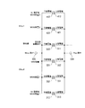
- the solid-state image sensor 100 includes a pixel array unit 110 and peripheral circuits for reading an electric signal from the pixel array unit 110 and performing predetermined signal processing.
- the solid-state image sensor 100 uses a row selection circuit 120 for controlling row address and row scanning, a horizontal transfer scanning circuit 130 for controlling column address and column scanning, and an internal clock as a control circuit as peripheral circuits.
- the timing control circuit 140 to be generated is provided.
- the solid-state imaging device 100 according to the first embodiment includes an ADC group 150 as peripheral circuits, a digital-to-analog converter (DAC) 160 as a lamp signal generator, an amplifier circuit 170, a signal processing circuit 180, and a horizontal circuit. It has a transfer line 190.
- the solid-state image sensor 100 according to the first embodiment has a DC power supply circuit (not shown) as a peripheral circuit.
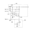
- the pixel array unit 110 is configured by arranging a large number of pixels 30 in an array shape (matrix shape).
- the pixel 30 has, for example, a photoelectric conversion element D1 made of, for example, a photodiode (PD), as shown in FIG.
- the pixel 30 has four transistors, a transfer transistor T1, a reset transistor T2, an amplification transistor T3, and a selection transistor T4, as active elements with respect to the photoelectric conversion element D1.
- the constant current source load 31 is connected to the vertical signal line (LSGN) in which the pixel 30 is shared in the column direction.
- LSGN vertical signal line
- the photoelectric conversion element D1 photoelectrically converts the incident light into an electric charge (electrons in this case) in an amount corresponding to the amount of the light.
- the transfer transistor T1 as a transfer element is connected between the photoelectric conversion element D1 and the floating diffusion FD as an input node, and a transfer signal TRG which is a control signal is given to the gate (transfer gate) through the transfer control line LTRG. .. As a result, the transfer transistor T1 transfers the electrons photoelectrically converted by the photoelectric conversion element D1 to the floating diffusion FD.
- the reset transistor T2 is connected between the power supply line L VDD to which the power supply voltage VDD is supplied and the floating diffusion FD, and the reset signal RST, which is a control signal, is given to the gate through the reset control line LRST.
- the reset transistor T2 as the reset element resets the potential of the floating diffusion FD to the potential of the power supply line L VDD.
- the gate of the amplification transistor T3 as an amplification element is connected to the floating diffusion FD. That is, the floating diffusion FD functions as an input node of the amplification transistor T3 as an amplification element.
- the amplification transistor T3 and the selection transistor T4 are connected in series between the power supply line L VDD to which the power supply voltage VDD is supplied and the signal line LSGN. In this way, the amplification transistor T3 is connected to the signal line LSGN via the selection transistor T4, and constitutes a constant current source IS outside the pixel portion and a source follower.
- the selection signal SEL which is a control signal corresponding to the address signal
- the selection transistor T4 is turned on.
- the amplification transistor T3 amplifies the potential of the floating diffusion FD and outputs a voltage corresponding to the potential to the signal line LSGN.
- the voltage output from each pixel through the signal line LSGN is output to the ADC group 150. Since, for example, the gates of the transfer transistor T1, the reset transistor T2, and the selection transistor T4 are connected in row units, these operations are performed simultaneously for each pixel for one row.
- the reset control line LRST, the transfer control line LTRG, and the selection control line LSEL wired to the pixel array unit 110 are wired as a set for each row of the pixel array.
- the reset control line LRST, the transfer control line LTRG, and the selection control line LSEL are provided with M lines each.
- the reset control line LRST, the transfer control line LTRG, and the selection control line LSEL are driven by the row selection circuit 120.
- a decoupling capacitor CV1 is connected between the power supply line L VDD and ground (GND).
- the decoupling capacitor CV1 removes noise components mixed in the DC power supply voltage supplied to drive the circuit.
- the total area of the decoupling capacitor CV1 may exceed 10 mm2, and it occupies a large proportion of the chip area of the laminated CMOS image sensor.
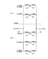
- the comparator 151 includes a differential amplifier circuit including differential input transistors T21 and T22 forming a differential pair and active load transistors T11 and T12 including a current mirror circuit.
- the differential input transistors T21 and T22 are composed of n-type MOSFETs (hereinafter, also referred to as “nMOS”), and the active load transistors T11 and T12 are composed of p-type MOSFETs (hereinafter, also referred to as “pMOS”).
- nMOS n-type MOSFETs
- pMOS p-type MOSFETs
- the active load transistors T11 and T12 and the differential input transistors T21 and T22 serve as noise sources.
- the comparator 151 includes a reference voltage (DAC side input) Vslop, which is a ramp waveform obtained by changing the reference voltage generated by the DAC 160 in a stepwise manner, and an analog signal obtained from a pixel via the vertical signal line LSGN for each line. (VSL (Vertical Signal Line) side input) is compared.
- VSL Very Signal Line
- the counter 152 shown in FIG. 1 counts the comparison time of the comparator 151.
- the ADC group 150 has an n-bit digital signal conversion function and is arranged for each vertical signal line (column line) to form a column-parallel ADC block.
- the output of each latch 153 is connected, for example, to a horizontal transfer line 190 having a width of 2 n bits. Then, 2n amplifier circuits 170 and signal processing circuits 180 corresponding to the horizontal transfer lines 190 are arranged.
- the sampling capacitances C1 and C2 shown in FIG. 4 can be miniaturized as the capacitance density (capacity value per unit area) of the capacitance element used increases, but the bias dependence of the capacitance value is required to be small. This is because if the bias dependence of the capacitance value is large, for example, the pixel signal and the reference signal transmitted to the gate electrode of the differential input transistor of the comparator are distorted, and the accuracy of analog-to-digital conversion is significantly deteriorated. Further, a decoupling capacitor CV2 is connected to the comparator 151 between the power supply line Vdd and the ground (GND).
- FIG. 5 shows a layout diagram of each circuit constituting the solid-state image sensor 100 according to the first embodiment on a semiconductor chip.
- a metal bonding portion 230 such as a TSV (Through-silicon via). It consists of a stacked image sensor in which a part of the wiring is electrically connected.
- the pixel array unit 110 in which the pixels 30 are arranged in a matrix is mounted on the upper semiconductor substrate 210, and peripheral circuits such as the ADC group 150 and the signal processing circuit 180 other than the pixel array unit 110 are mounted on the lower semiconductor substrate 220. Will be done.
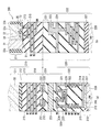
- FIG. 6 is a cross-sectional view of the solid-state image sensor 100 according to the first embodiment.
- FIG. 6A shows the outside of the pixel
- FIG. 6B shows the inside of the pixel.
- the upper semiconductor substrate 210 is composed of a photoelectric conversion layer 211, an inter-glabellar insulating film 213, and a wiring layer 214 from the top.
- the photoelectric conversion layer 211 is a layer on which a photodiode (PD) 31 is formed, and generates an electric charge according to the amount of incident light by photoelectric conversion.
- the PD 31 is electrically separated by the element separation portions 33a and 33b formed in the photoelectric conversion layer 211 for each pixel 30.
- a p-type well 32 is formed in the region in the photoelectric conversion layer 211 where the PD 31 is not formed.
- the FD34 and the n-type diffusion layer 35 are formed in the p-type well 32.
- the p-type well 32 is provided outside the pixel 30, as shown in FIG. 6A.
- the electric charge generated in the PD 31 is transferred to the FD 34 via the transfer transistor T1 provided in the glabellar insulating film 213.
- An amplification transistor T3 provided in the glabellar insulating film 213 is located near the n-type diffusion layer 35.
- Element separation portions 33b and 33c are formed at both ends of the n-type diffusion layer 35.
- the FD 34 and the pixel transistor T3 are electrically separated by the n-type diffusion layer 35 and the element separation portions 33b and 33c.
- the wiring layer 214 is configured to include wirings (M1 to M4) 215 laminated in a plurality of layers.
- the transfer transistor T1, the reset transistor T2, the amplification transistor T3, and the selection transistor T4 constituting each pixel 30 are driven via the plurality of layers of wiring (M1 to M4) 215 formed on the wiring layer 214.
- a copper (Cu) metal bonding portion 231 is provided in the wiring layer 214 to bond the metal bonding portion 231 to the lower semiconductor substrate 220.
- the lower semiconductor substrate 220 is composed of the glabella insulating film 221 and the wiring layer 222 from the top.
- the wiring layer 222 includes all wirings 223 and wirings (M1 to M6) 224 laminated in a plurality of layers.
- the inter-eyebrow insulating film 221 is provided with a copper (Cu) metal bonding portion 232 for bonding with the metal bonding portion 231 of the upper semiconductor substrate 210.
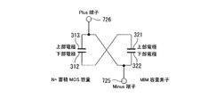
- an N + storage type MOS capacitive element 310 is arranged on the lower semiconductor substrate 220.
- the lower electrode 312 mounted on the element separating portion 311 is It is an n-type diffusion layer formed in the p-type well 228, and a gate insulating film 316 made of silicon oxide (SiO2) is placed on the lower electrode 312 thereof, and the gate insulating film 316 is placed on the gate insulating film 316.
- An upper electrode 313 made of n-type polycrystalline silicon is formed.
- This MOS capacitance element 310 is called an N + storage type MOS capacitance because electrons are accumulated on the surface of the lower electrode 312 during operation.
- the lower electrode 322 located on the side closer to the lower semiconductor substrate 220 side and the insulating film (High). (Including -K material) and a MIM (Metal Insulator Metal) capacitive element 320 formed by laminating the upper electrode 321 are mounted.
- This insulating film is any one of Ta2O2, Nb2O3, Zr02, HfO2, La2O3, Pr2O3, AL2O3, SiO2, and SiN, or a plurality of laminated films.
- the lower electrode 322 and the upper electrode 321 are a single-layer film of any one of Cu, Al, Ti, TiN, Ta, and TaN, or a plurality of laminated films.
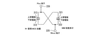
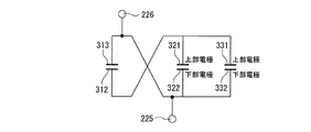
- the wiring (M5) 224 is provided with a negative (Minus) terminal 225 and a positive (Plus) terminal 226.
- the comb-shaped wiring (MOM) capacitance element 330 shown in FIG. 8 and the PIP (Poly Insulator Poly) capacitance element 340 shown in FIG. 10 may be used.
- the lower electrode 312 of the N + storage type MOS capacitance element 310 and the upper electrode 321 of the MIM capacitance element 320 are connected by a via 315 and a wiring (M6) 224, and the MOS capacitance element 310
- the MOS capacitance element 310 By connecting the upper electrode 313 and the lower electrode 322 of the MIM capacitance element 320 with the via 314 and the wiring (M5) 224, the two capacitance elements are connected in parallel.
- the first merit is that the capacitance density per unit area of the capacitive element increases. For example, if the capacitance value when the potential difference between the electrodes of the MOS capacitance element 310 is 3 V is 100 fF and the capacitance value when the potential difference between the electrodes of the MIM capacitance element 320 is 3 V is 100 fF, the two MOS capacitances are When the element 310 and the MIM capacitance element 320 are connected in parallel and operated at 3V, the capacitance value becomes 200 fF, and the capacitance density doubles.
- the TDDB can reduce the capacitance density without shortening the life as compared with the case where the film thickness of the insulating film between the electrodes of the MOS capacitive element 310 and the MIM capacitive element 320 is thinned to increase the capacitance density. Can be increased.
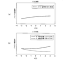
- FIG. 12A shows the CV characteristics of the N + storage type MOS capacitive element 310.
- the horizontal axis shows the potential difference between the electrodes, and the vertical axis is the value standardized by the capacitance value when the potential difference is -3V.
- the bias dependence of the capacitance value has a positive slope as shown by the solid line A.
- the CV characteristic of the MIM capacitance element 320 has a positive inclination as shown in FIG.
- the CV characteristic shows A // C in FIG. 13, and it is possible to form a capacitance element having a small voltage dependence of the capacitance value.
- FIG. 6 shows an example in which two different MOS capacitance elements 310 and MIM capacitance element 320 are arranged in the same area, but it is not always necessary to arrange them in the same area.
- the MIM capacitance element 320 having a characteristic opposite to the CV characteristic of the MOS capacitance element 310 is connected in parallel to the N + storage type MOS capacitance element 310. Therefore, the bias characteristics are canceled out, and a capacitive element having a flat bias characteristic is realized. Further, the capacitance density can be increased without shortening the life of the TDDB, as compared with the case where the film thickness of the insulating film between the electrodes of the capacitance element is thinned to increase the capacitance density.
- each capacitance element having a small bias dependence of the capacitance value and a large capacitance density without lowering the operating voltage.
- the device structure and size of each capacitance element and the connection method of each capacitance element can be optimized so that the CV characteristic of the entire capacitance element is closest to 1.
- FIG. 14 is a cross-sectional view of the solid-state image sensor 100 according to the first modification of the first embodiment.
- the same parts as those in FIG. 6A are designated by the same reference numerals, and detailed description thereof will be omitted.
- the solid-state imaging device 100 forms the MOM capacitance element 330 shown in FIG. 8 on the lower semiconductor substrate 220 by using the wirings (M1 to M4) 224, and forms them with N + storage type MOS capacitance.
- the structure is such that the element 310 and the MIM capacitance element 320 are connected in parallel.
- the upper electrode 331 of the MOM capacitance element 330 is via the lower electrode 312 of the MOS capacitance element 310, the upper electrode 321 of the MIM capacitance element 320, the via 315, and the wiring (M6) 224. Is connected.
- the lower electrode 332 of the MOM capacitance element 330 is connected to the upper electrode 313 of the MOS capacitance element 310 and the lower electrode 322 of the MIM capacitance element 320 via the via 314 and the wiring (M6) 224. With such a structure, the capacitance density can be further increased.
- the CV characteristic of the general MOM capacitance element 330 has a very small bias dependence of the capacitance value regardless of the positive or negative of the bias applied between the electrodes. In this state, it is equivalent to the CV characteristic when the N + storage type MOS capacitance element 310 and the MIM capacitance element 320 shown in FIG. 16A are connected in parallel. Therefore, even if such a MOM capacitance element 330 is added to the capacitance element in which the capacitance element 330 is connected in parallel, the bias dependence of the capacitance value of the entire capacitance element is not significantly increased. Further, since the bias dependence of the capacitance value described above does not change significantly depending on whether the bias applied between the electrodes is positive or negative, it is not necessary to be aware of the electrode connection method, and which electrode is connected to the positive (Plus) terminal 226. good.
- FIG. 17 is a cross-sectional view of the solid-state image sensor 100 according to the second modification of the first embodiment.
- the same parts as those in FIG. 6A are designated by the same reference numerals, and detailed description thereof will be omitted.
- the solid-state image sensor 100 utilizes a Hall storage type MOS capacitance element 360 (referred to as P + storage type MOS capacitance).
- the lower electrode 362 near the lower semiconductor substrate 220 side is a P-type diffusion layer formed in the n-type well 229, and silicon oxide (SiO2) is placed on the lower electrode 362.
- silicon oxide SiO2
- the upper electrode 363 of the MOS capacitive element 360 is connected to the upper electrode 321 of the MIM capacitive element 320 via the via 364 and the wiring (M6) 224.
- the lower electrode 362 of the MOS capacitance element 360 is connected to the lower electrode 322 of the MIM capacitance element 320 via the via 365 and the wiring (M6) 224.
- the CV characteristic has a negative sign of bias dependence of the capacitance value when the lower electrode 362 is fixed to 0V and the potential of the upper electrode 363 is changed by -3V to 3V. (Dotted line D).
- the bias dependence sign of the capacitance value becomes positive (solid line B). Therefore, by connecting the upper electrodes and the lower electrodes of the two capacitance elements 320 and 360 in parallel, it is possible to reduce the bias dependence of the capacitance value.
- FIG. 20 is a cross-sectional view of the solid-state image sensor 100 according to the third modification of the first embodiment.
- the same parts as those in FIG. 6A are designated by the same reference numerals, and detailed description thereof will be omitted.
- the electrodes of two MIM capacitive elements 320 and 350 formed in different layers are connected in reverse.
- the lower electrode 322 of the MIM capacitance element 320 is connected to the upper electrode 351 of the MIM capacitance element 350 via the wiring (M4) 224 and the wiring (M6) 224.
- the upper electrode 321 of the MIM capacitance element 320 is connected to the lower electrode 352 of the MIM capacitance element 350 via the wiring (M3) 224 and the wiring (M6) 224.
- the bias dependence of the capacitance value of the capacitance element in which the upper electrode 321 of the MIM capacitance element 320 and the lower electrode 352 of the MIM capacitance element 350 are connected and connected in parallel has a different sign of the bias dependence of the capacitance value in each element. Therefore, it is possible to reduce the bias dependence of the capacitance value.
- FIG. 23 is a cross-sectional view of the solid-state image sensor 100 according to the fourth modification of the first embodiment.
- the same parts as those in FIG. 6A are designated by the same reference numerals, and detailed description thereof will be omitted.
- the solid-state image sensor 100 is an example utilizing a PIP (PolyInsulatorPoly) capacitive element 340.
- the PIP capacitive element 340 is a capacitive element using polycrystalline silicon as an electrode.
- an N-type polycrystalline Si as a lower electrode 342, SiO2 as an insulating film, and N as an upper electrode.
- It is a capacitive element formed by sequentially laminating type polycrystalline Si. As a feature, the bias dependence of the capacitance value is small.
- the upper electrode 343 of the PIP capacitance element 340 is connected to the lower electrode 352 of the MIM capacitance element 350 via the wiring (M3) 224. Further, the lower electrode 342 of the PIP capacitance element 340 is connected to the upper electrode 351 of the MIM capacitance element 350 via the wiring (M4) 224.
- the MOM capacitive element 330 when applied to the first embodiment of the present disclosure, it plays the same role as the MOM capacitive element 330. That is, by adding the PIP capacitance element 340 to one of the capacitance elements connected in parallel, as shown in FIG. 25, the capacitance of the entire capacitance element does not change significantly without significantly changing the bias dependence of the capacitance value of the entire capacitance element. The value can be increased. In the case of parallel connection, either the lower electrode 342 or the upper electrode 343 may be connected to the positive side (Plus) as in the case of the MOM capacitive element 330.
- the upper electrode 313 of the MOS capacitance element 310 and the upper electrode 363 of the MOS capacitance element 360 are connected in parallel.
- the lower electrode 312 of the MOS capacitance element 310 and the lower electrode 362 of the MOS capacitance element 360 need only be connected in parallel.
- FIG. 26 is a cross-sectional view of the solid-state image sensor 100 according to the second embodiment.
- the same parts as those in FIG. 14 are designated by the same reference numerals, and detailed description thereof will be omitted.
- the capacitance element is mounted on both chips of the upper semiconductor substrate 210 and the lower semiconductor substrate 220, and the upper semiconductor substrate 210 is used by using the metal bonding portion 230 arranged on the bonding surface.
- the capacitive elements mounted on the lower semiconductor substrate 220 are connected in parallel.
- the upper semiconductor substrate 210 is composed of a p-type well 32, an inter-glabellar insulating film 213, and a wiring layer 214 from the top.
- An N + storage type MOS capacitive element 410 is arranged below the upper semiconductor substrate 210. Assuming that the electrode closer to the lower semiconductor substrate 220 side on which the MOS capacitance element 410 is mounted is the lower electrode 412, the lower electrode 412 is an n-type diffusion layer formed in the p-type well 32.
- a gate insulating film 416 made of silicon oxide (SiO2) is placed on the lower electrode 412, and an upper electrode 413 made of n-type polycrystalline silicon is formed on the gate insulating film 416.
- the wiring (M1 to M4) 215 is used in the MOM.
- a capacitive element 420 is formed.
- the upper electrode 421 of the MOM capacitance element 420 is connected to the upper electrode 413 of the MOS capacitance element 410 via the via 414.
- the lower electrode 422 of the MOM capacitance element 420 is connected to the lower electrode 412 of the MOS capacitance element 410 via the via 415.
- the upper electrode 413 of the MOS capacitance element 410 and the upper electrode 421 of the MOM capacitance element 420 are connected to the upper electrode of the MOS capacitance element 310 on the lower semiconductor substrate 220 side via the copper (Cu) metal coupling portions 231 and 232.
- the 313, the lower electrode 322 of the MIM capacitance element 320, and the upper electrode 331 of the MOM capacitance element 330 are connected.
- the lower electrode 412 of the MOS capacitance element 410 and the lower electrode 422 of the MOM capacitance element 420 are connected to the lower electrode of the MOS capacitance element 310 on the lower semiconductor substrate 220 side via the copper (Cu) metal coupling portions 231 and 232.
- the 312, the upper electrode 321 of the MIM capacitance element 320, and the lower electrode 332 of the MOM capacitance element 330 are connected.
- the bias-dependent code of the capacitance value of each capacitive element is N + accumulation.
- the type MOS capacitance elements 310 and 410 are positive, and the MIM capacitance element 320 is negative.
- the N + storage type MOS capacitance elements 310 and 410 and the MIM capacitance element 320 have opposite bias-dependent inclination signs, so optimize these element sizes. For example, it is possible to make the bias dependence of the capacitance value of the entire capacitance element formed by connecting these in parallel very small.
- the capacitance values of the MOS capacitance element 410 and the MOM capacitance element 420 of the upper semiconductor substrate 210 (sensor unit) can be added as compared with the first embodiment.
- the N + storage type MOS capacitance element 310 and the N + storage type MOS capacitance element 410 are 100 fF
- the capacitance values of the MOM capacitance element 330 and the MOM capacitance element 420 are 30 fF
- the MIM capacitance element 320 is 100 fF.
- the total capacitance value of the parallel capacitance element is 3.6 times the capacitance value of the N + storage type MOS capacitance element 310 alone.
- FIG. 28 is a cross-sectional view of the solid-state image sensor 100 according to the first modification of the second embodiment.
- the same parts as those in FIG. 26 are designated by the same reference numerals, and detailed description thereof will be omitted.
- the solid-state imaging device 100 mounts the same N + storage type MOS capacitance element 310 and MOM capacitance element 330 as in the first embodiment on the lower semiconductor substrate 220 (peripheral circuit portion), and mounts the upper semiconductor substrate.
- the 210 sensor unit
- the 210 is equipped with a P + storage type MOS capacitance element 430 and a MOM capacitance element 420.
- the MOS capacitive element 430 the lower electrode 431 near the upper semiconductor substrate 210 side is a P-type diffusion layer, and a gate insulating film 436 made of silicon oxide (SiO2) is provided on the lower electrode 431.
- An upper electrode 432 made of P-type polycrystalline silicon is formed on the gate insulating film 436.
- the upper electrode 421 of the MOM capacitance element 420 is connected to the upper electrode 432 of the MOS capacitance element 430 via the via 414. Further, the lower electrode 422 of the MOM capacitance element 420 is connected to the lower electrode 431 of the MOS capacitance element 430 via the via 415.
- the upper electrode 432 of the MOS capacitance element 430 and the upper electrode 421 of the MOM capacitance element 420 are connected to the upper electrode of the MOS capacitance element 310 on the lower semiconductor substrate 220 side via the copper (Cu) metal coupling portions 231 and 232.
- the 313 is connected to the upper electrode 331 of the MOM capacitive element 330.
- the lower electrode 431 of the MOS capacitance element 430 and the lower electrode 422 of the MOM capacitance element 420 are the lower electrodes of the MOS capacitance element 310 on the lower semiconductor substrate 220 side via the metal coupling portions 231 and 232 made of copper (Cu).
- the 312 is connected to the lower electrode 332 of the MOM capacitive element 330.
- FIG. 30 is a cross-sectional view of the solid-state image sensor 100 according to the second modification of the second embodiment.
- the same parts as those in FIG. 30 are designated by the same reference numerals, and detailed description thereof will be omitted.
- the solid-state imaging device 100 functions as a capacitive element by facing the metal bonding portion 511 on the upper semiconductor substrate 210 side and the metal bonding portion 512 on the lower semiconductor substrate 220 side arranged on the bonding surface. Is connected in parallel with other capacitance elements to further increase the capacitance density.
- This capacitive element is called a junction capacitive element 510.
- the metal bonding portion 511 on the upper semiconductor substrate 210 side is used as the upper electrode
- the metal bonding portion 512 on the lower semiconductor substrate 220 side is used as the lower electrode.
- the upper electrode (metal bonding portion 511) of the junction capacitance element 510 is connected to the upper electrode 413 of the MOS capacitance element 410, the upper electrode 421 of the MOM capacitance element 420, and via via 414.
- the lower electrode (metal bonding portion 512) of the junction capacitance element 510 is connected to the lower electrode 412 of the MOS capacitance element 410 and the lower electrode 422 of the MOM capacitance element 420 via the via 415.
- the upper electrode (metal coupling portion 511) of the junction capacitance element 510 includes the upper electrode 313 of the MOS capacitance element 310 on the lower semiconductor substrate 220 side, the lower electrode 322 of the MIM capacitance element 320, and the MOM capacitance element 330. It is connected to the upper electrode 331.
- the lower electrode (metal coupling portion 512) of the junction capacitance element 510 includes the lower electrode 312 of the MOS capacitance element 310 on the lower semiconductor substrate 220 side, the upper electrode 321 of the MIM capacitance element 320, and the MOM capacitance element 330. It is connected to the lower electrode 332.
- the junction capacitance element 510 has the function of a capacitance element by facing metal materials, and the bias dependence of the capacitance value is very small like the MOM capacitance elements 330 and 420. Therefore, by connecting the junction capacitance elements 510 in parallel, the bias dependence of the capacitance value of the connection source capacitance element does not change significantly, and the capacitance density increases.
- the metal coupling portions 511 and 512 of the upper semiconductor substrate 210 and the lower semiconductor substrate 220 are formed as the junction capacitance element 510, thereby forming the capacitance element.
- the overall capacity value can be increased.
- FIG. 32 is a table showing capacitive elements that can be mounted on the upper semiconductor substrate 210 (Chip1) and the lower semiconductor substrate 220 (Chip2) by using a general CMOS process.
- connection direction of the electrodes of the table in FIG. 32 is "positive" when the upper electrode of each capacitance element is connected to the Plus terminal and the lower electrode is connected to the negative (Minus) terminal 225.
- the case where the upper electrode of each capacitance element is connected to the negative (Minus) terminal 225 and the lower electrode is connected to the positive (Plus) terminal 226 is “reverse”. Elements that have a very small bias dependence of the capacitance value and that can be connected to either terminal without any problem are described as "no matter”.
- the sign of the bias-dependent slope of the capacitance value is that the negative (Minus) terminal 225 is described as 0V and the positive (Plus) terminal 226 is changed by -3 to 3V in the connection described in the electrode connection direction. It is a bias-dependent code of the capacitance value at the time. From the table of FIG. 32, in a laminated structure in which two chips are laminated, a plurality of capacitive elements can be connected in parallel by a desired connection method to achieve both the capacitance density set in Target and the bias dependence of the capacitance value. There are numerous combinations. Although not all combinations thereof can be described in the embodiment, the designer makes an optimum selection in consideration of the characteristics required for the circuit to be designed, the available Chip area, and the manufacturing cost for mounting each element. Just do.
- a photoelectric conversion element and an amplification transistor for amplifying a signal from the photoelectric conversion element are arranged on different substrates, and a sensor unit in which the photoelectric conversion element and the transfer gate (TRG) are arranged and amplification are provided.
- TRG transfer gate
- a solid-state imaging device in which three substrates on which a pixel transistor portion in which a pixel transistor such as a transistor is arranged and a peripheral circuit portion in which a signal processing circuit for processing a signal from an amplification transistor is arranged are laminated by WoW technology will be described.
- FIG. 33 is a cross-sectional view of the solid-state image sensor 100A according to the third embodiment.
- FIG. 33 (a) shows the outside of the pixel
- FIG. 33 (b) shows the inside of the pixel.
- the same parts as those in FIG. 26 are designated by the same reference numerals, and detailed description thereof will be omitted.
- the solid-state image sensor 100A is composed of a sensor unit 610, a pixel transistor unit 620, and a peripheral circuit unit 630 from the top.
- a sensor unit 610 In the solid-state image sensor 100A, three semiconductor chips of a sensor unit 610, a pixel transistor unit 620, and a peripheral circuit unit 630 are superposed, and a part of the wiring is electrically connected by a metal coupling unit 640. It is composed of stacked image sensors that are connected to each other.
- the transfer transistor T1, the photoelectric conversion element D1, and the floating diffusion FD34 are arranged in the sensor unit 610.
- a reset transistor T2, an amplification transistor T3, and a selection transistor T4 are arranged in the pixel transistor section 620.
- the sensor unit 610 is composed of the photoelectric conversion layer 611 and the glabella insulating film 612 from above.
- the photoelectric conversion layer 211 is a layer on which a photodiode (PD) 31 is formed, and generates an electric charge according to the amount of incident light by photoelectric conversion.
- the PD 31 is electrically separated by element separation portions 33a and 33b formed in the photoelectric conversion layer 611 for each pixel 30.
- the FD34 and the gate electrode 36 of the transfer transistor T1 are formed on the photoelectric conversion layer 611.
- a transfer transistor T1 is formed on the glabellar insulating film 612.
- the pixel transistor section 620 is composed of a p-type well 621 and a wiring layer 622 from the top. An n-type diffusion layer is formed in the p-type well 621.
- the wiring layer 622 includes wirings (M1 to M4) 623 laminated in a plurality of layers.
- the transfer transistor T1, the reset transistor T2, the amplification transistor T3, and the selection transistor T4 constituting each pixel 30 are driven via the plurality of layers of wiring (M1 to M4) 623 formed on the wiring layer 622. Further, a copper (Cu) metal bonding portion 641 is provided in the wiring layer 622 to join the peripheral circuit portion 630.
- Cu copper
- the peripheral circuit unit 630 is composed of an inter-glabellar insulating film and a wiring layer from above.
- the wiring layer includes all wirings 631 and wirings (M1 to M6) 632 laminated on a plurality of layers.
- the glabellar insulating film is provided with a copper (Cu) metal bonding portion 642 for bonding with the metal bonding portion 641 of the pixel transistor portion 620.
- the generated charge is a pixel signal on the signal line LSGN shown in FIG. 1 formed by the wiring (M1 to M4) 623 and the wiring (M1 to M6) 632 of the peripheral circuit unit 630 via the amplification transistor T3. Is output to the ADC group 150 formed in the peripheral circuit unit 630.
- an N + storage type MOS capacitive element 310 is arranged on the peripheral circuit unit 630.
- the MOM capacitance element 330 and the MIM capacitance element 320 are arranged on the upper layer of the MOS capacitance element 310.
- An N + storage type MOS capacitive element 410 is arranged below the pixel transistor section 620.
- the wiring (M1 to M4) 623 is used for MOM.
- a capacitive element 420 is formed.
- the upper electrode 421 of the MOM capacitance element 420 is connected to the upper electrode 413 of the MOS capacitance element 410 via the via 414.
- the lower electrode 422 of the MOM capacitance element 420 is connected to the lower electrode 412 of the MOS capacitance element 410 via the via 415.
- the upper electrode 413 of the MOS capacitance element 410 and the upper electrode 421 of the MOM capacitance element 420 are connected to the upper electrode 313 of the MOS capacitance element 310 on the peripheral circuit portion 630 side via the copper (Cu) metal coupling portions 641 and 642.
- the lower electrode 322 of the MIM capacitance element 320 and the upper electrode 331 of the MOM capacitance element 330 are connected.
- the lower electrode 412 of the MOS capacitance element 410 and the lower electrode 422 of the MOM capacitance element 420 are connected to the lower electrode 312 of the MOS capacitance element 310 on the peripheral circuit portion 630 side via the copper (Cu) metal coupling portions 641 and 642.
- the upper electrode 321 of the MIM capacitance element 320 and the lower electrode 332 of the MOM capacitance element 330 are connected.
- the negative (Minus) terminal 225 is fixed to 0V
- the positive (Plus) terminal 226 is set to -3 to -3 to 3.
- the bias-dependent codes of the capacitance values of the respective capacitance elements when changed by 3 V are the N + storage type MOS capacitance element 310 and the N + storage type MOS capacitance element 410. It is positive and the MIM capacitive element 320 becomes negative.
- the N + storage type MOS capacitance element 310 and the N + storage type MOS capacitance element 410 and the MIM capacitance element 320 have opposite bias-dependent inclination signs.
- the three-layer laminated image sensor can also be equipped with a capacitance element having a large capacitance value and a small bias dependence of the capacitance value.
- a fourth embodiment of the present disclosure describes a solid-state image sensor applied to a photodetector using a SPAD (Single Photon Avalanche Diode).
- FIG. 37 shows a layout diagram of each circuit constituting the solid-state image sensor 100B according to the fourth embodiment on the semiconductor chip.
- a metal bonding portion 730 such as a TSV (Through-silicon via). It consists of a stacked image sensor in which a part of the wiring is electrically connected.
- the SPAD photodiodes 41 are arranged in a matrix on the upper semiconductor substrate 710, and peripheral circuits 51 such as the ADC group 150 and the signal processing circuit 180 other than the SPAD photodiode 41 are mounted on the lower semiconductor substrate 720.
- FIG. 38 is a cross-sectional view of the solid-state image sensor 100B according to the fourth embodiment.
- FIG. 38 (a) shows the outside of the pixel
- FIG. 38 (b) shows the inside of the pixel.
- the upper semiconductor substrate 710 is composed of a photoelectric conversion layer 711, an inter-glabellar insulating film 713, and a wiring layer 714 from the top.
- the photoelectric conversion layer 711 is a layer on which a SPAD photodiode 41 is formed, detects incident light (photons), and converts carriers generated thereby into electrical signal pulses using avalanche multiplier.
- the SPAD photodiode 41 is electrically separated by a p-type diffusion layer 42a and an n-type diffusion layer 42b formed in the photoelectric conversion layer 711 for each pixel 30.
- a p-type diffusion layer 42a is electrically separated by a p-type diffusion layer 42a and an n-type diffusion layer 42b formed in the photoelectric conversion layer 711 for each pixel 30.
- p-type well 43 is provided outside the pixel 30, as shown in FIG. 38 (a).
- the electric signal pulse generated from the SPAD photodiode 41 is output to the wiring (M1 to M4) 715 formed in the wiring layer 714 via the via 716 formed in the inter-glabella insulating film 713.
- a copper (Cu) metal bonding portion 731 is provided in the wiring layer 714 to bond the metal bonding portion 731 to the lower semiconductor substrate 720.
- the lower semiconductor substrate 720 is composed of the glabella insulating film 721 and the wiring layer 722 from the top.
- the wiring layer 722 includes all wirings 723 and wirings (M1 to M6) 724 laminated in a plurality of layers.
- the inter-eyebrow insulating film 721 is provided with a copper (Cu) metal bonding portion 732 for bonding with the metal bonding portion 731 of the upper semiconductor substrate 710.
- the light detected by the upper semiconductor substrate 210 is photoelectrically converted by the SPAD photodiode 41 to generate an electric signal pulse. Then, the electric signal pulse is output to the peripheral circuit 51 via the signal line LSGN shown in FIG. 1 formed by the wiring (M1 to M4) 715 and the wiring (M1 to M6) 724 of the lower semiconductor substrate 720. ..
- an N + storage type MOS capacitive element 310 is arranged on the lower semiconductor substrate 720.
- the lower electrode 322 located on the side closer to the lower semiconductor substrate 220 side and the insulating film (High). (Including -K material) and a MIM (Metal Insulator Metal) capacitive element 320 formed by laminating the upper electrode 321 are mounted.
- the lower electrode 312 of the N + storage type MOS capacitance element 310 and the upper electrode 321 of the MIM capacitance element 320 are connected by a via 315 and a wiring (M6) 724, and the MOS capacitance element 310
- the MOS capacitance element 310 By connecting the upper electrode 313 and the lower electrode 322 of the MIM capacitance element 320 with the via 314 and the wiring (M5) 724, the two capacitance elements are connected in parallel.
- the semiconductor device according to the present technology can be applied to a capacitor constituting a general filter circuit.
- a general filter circuit includes a resistor R11 and a capacitor C11, and a semiconductor device according to the present technology can be applied as a configuration of the capacitor C11.
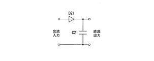
- a general filter circuit includes a diode D21 and a capacitor C21, and a semiconductor device according to the present technology can be applied as a configuration of the capacitor C21.
- a general integral circuit includes a resistor R32, a capacitor C31, and an operational amplifier 800, and a semiconductor device according to the present technology can be applied as a configuration of the capacitor C31.
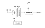
- FIG. 43 is a schematic configuration diagram of the electronic device 1000 according to the sixth embodiment of the present disclosure.
- the electronic device 1000 according to the sixth embodiment includes a solid-state imaging device 1010, an optical lens 1020, a shutter device 1030, a drive circuit 1040, and a signal processing circuit 1050.
- the electronic device 1000 of the sixth embodiment shows an embodiment in which the solid-state image sensor 100 according to the first embodiment of the present disclosure is used as an electronic device (for example, a camera) as the solid-state image sensor 1010.
- the optical lens 1020 forms an image of image light (incident light 1060) from the subject on the image pickup surface of the solid-state image pickup device 1010. As a result, the signal charge is accumulated in the solid-state image sensor 1010 for a certain period of time.
- the shutter device 1030 controls the light irradiation period and the light blocking period of the solid-state image sensor 1010.
- the drive circuit 1040 supplies a drive signal for controlling the transfer operation of the solid-state image sensor 1010 and the shutter operation of the shutter device 1030.
- the signal transfer of the solid-state image sensor 1010 is performed by the drive signal (timing signal) supplied from the drive circuit 1040.
- the signal processing circuit 1050 performs various signal processing on the signal (pixel signal) output from the solid-state imaging device 1010.
- the video signal after signal processing is stored in a storage medium such as a memory or output to a monitor.
- the optical color mixing is suppressed in the solid-state image sensor 1010, so that the image quality of the video signal can be improved.
- the electronic device 1000 to which the solid-state image sensors 100, 100A, and 100B can be applied is not limited to the camera, but can be applied to other electronic devices. For example, it may be applied to an imaging device such as a camera module for mobile devices such as mobile phones.
- the solid-state image sensors 100, 100A, and 100B according to the first to fourth embodiments are used for the electronic device, but other configurations may be used.
- the present disclosure may also have the following structure.
- (1) With a semiconductor substrate The first capacitive element laminated on the semiconductor substrate and It is provided with a second capacitive element that is laminated on the side of the first capacitive element opposite to the semiconductor substrate side and has a characteristic opposite to the bias characteristic of the capacitance value of the first capacitive element.
- the first capacitive element and the second capacitive element are semiconductor devices connected in parallel.
- (2) The first and second capacitive elements are provided with n (n is an integer).
- the capacitance value of the entire element when the potential difference between the electrodes is the operating voltage is set to Capital (V)
- the capacitance value of the entire element when the potential difference between the electrodes is 0 is set to Total (0), and each capacitance is set.
- the semiconductor device is a first conductive type storage type MOS capacitive element having a lower electrode formed on the semiconductor substrate side and an upper electrode facing the lower electrode with an insulating film interposed therebetween.
- the second capacitive element has a lower electrode formed on the semiconductor substrate side and an upper electrode facing the lower electrode with an insulating film interposed therebetween, and has the opposite polarity to that of the first conductive type.
- the second conductive type storage type MOS capacitance element of The upper electrode of the first conductive type storage type MOS capacitance element is connected to the upper electrode of the second conductive type storage type MOS capacitance element, and the lower electrode of the first conductive type storage type MOS capacitance element is connected.
- the first capacitive element is a first conductive type storage type MOS capacitive element having a lower electrode formed on the semiconductor substrate side and an upper electrode facing the lower electrode with an insulating film interposed therebetween.
- the second capacitive element is a MIM (Metal Insulator Metal) capacitive element having a lower electrode formed on the semiconductor substrate side and an upper electrode facing the lower electrode with an insulating film interposed therebetween.
- the upper electrode of the first conductive type storage type MOS capacitance element and the lower electrode of the MIM capacitance element are connected, and the lower electrode of the first conductive type storage type MOS capacitance element and the upper part of the MIM capacitance element are connected.
- the semiconductor device which includes a parallel connection structure for connecting electrodes.
- the first capacitive element has a lower electrode formed on the semiconductor substrate side and an upper electrode facing the lower electrode with an insulating film interposed therebetween, and has a polarity opposite to that of the first conductive type. It is a second conductive type storage type MOS capacitance element.
- the second capacitive element is a MIM capacitive element having a lower electrode formed on the semiconductor substrate side and an upper electrode facing the lower electrode with an insulating film interposed therebetween.
- the upper electrode of the second conductive type storage type MOS capacity element and the upper electrode of the MIM capacity element are connected, and the lower electrode of the second conductive type storage type MOS capacity element and the lower part of the MIM capacity element are connected.
- the first capacitive element is a first MIM capacitive element having a lower electrode formed on the semiconductor substrate side and an upper electrode facing the lower electrode with an insulating film interposed therebetween.
- the second capacitive element is a second MIM capacitive element having a lower electrode formed on the semiconductor substrate side and an upper electrode facing the lower electrode with an insulating film interposed therebetween.
- the semiconductor device according to (1) or (2) above which includes a parallel connection structure for connecting the above.
- the semiconductor device according to any one of (1) to (6) above which includes a structure in which comb-shaped wiring capacitance elements are connected in parallel.
- the semiconductor device according to any one of (1) to (7) above further comprising a structure in which PIP (Poly Insulator Poly) type capacitive elements are connected in parallel.
- Another semiconductor substrate having a third capacitive element is provided.
- the other semiconductor substrate is bonded to the semiconductor substrate, and the bias characteristic of the capacitance value of the entire capacitance element of the first capacitance element, the second capacitance element, and the third capacitance element is closest to 1.
- the semiconductor device according to (9) above which includes a structure in which a junction between the semiconductor substrate and the other semiconductor substrate is a capacitive element.
- the semiconductor substrate has at least one of a pixel and a peripheral circuit that processes a signal from a pixel transistor that amplifies the signal from the pixel.
- the pixel consists of a photodiode
- the semiconductor substrate having the peripheral circuit includes a first semiconductor substrate having the pixel transistor and a second semiconductor substrate having the peripheral circuit.
- the semiconductor substrate has at least one of a sensor unit having a SPAD (Single Photon Avalanche Diode) photodiode and a peripheral circuit for processing a signal from the sensor unit.
- SPAD Single Photon Avalanche Diode
- the first capacitive element laminated on the semiconductor substrate and The first capacitive element is laminated on the side opposite to the semiconductor substrate side, and includes a second capacitive element having a characteristic opposite to the bias characteristic of the capacitance value of the first capacitive element.
- the first capacitive element and the second capacitive element are provided with a semiconductor device connected in parallel. Electronics.
- Horizontal transfer line 210, 710 ... Upper semiconductor substrate, 211, 611, 711 ... Photoelectric conversion layer, 213,221,612,713,721 ... Intereural insulating film, 215,223,224,623,631,632,715,723,724 ... Wiring, 214,222,622,714, 722 ... Wiring layer, 220, 720 ... Lower semiconductor substrate, 225 ... Negative terminal, 226 ... Positive terminal, 230, 231,232, 511, 512,640, 641, 642,730, 731, 732 ... Metal joint, 310, 360 ... MOS capacitive element, 312,322,332 ... lower electrode, 313,321,331 ... upper electrode, 314,315,716 ...
Abstract
Description
なお、半導体基板上に形成する容量素子としては、特許文献2に示したMOS型容量素子、特許文献3に示した櫛形配線容量素子、特許文献4に示したMIM(Metal Insulator Metal)容量素子の使用が提案されている。 In addition, the shift to the fine process of the CMOS process for manufacturing peripheral circuit parts has been progressing for some time. However, even if the process shifts to a fine process, the logic circuit that processes digital signals composed of MOSFETs such as SRAM and logic circuits can be miniaturized, but the analog circuit that processes analog signals output from the sensor unit is compact. It is not easy to convert. The reason is that the larger the maximum amount of charge that can be read out by the sensor unit, the better the performance of the image sensor, but the detected amount of charge is converted to voltage and propagates through the circuit, so the generation of the manufacturing process is miniaturized. However, as long as the performance of the maximum charge amount is maintained, the operating voltage of the device constituting the analog circuit that receives the signal of the sensor unit does not decrease, and the device itself cannot be miniaturized according to the scaling law. ..
The capacitive elements formed on the semiconductor substrate include the MOS type capacitive element shown in
この場合、各容量素子間の容量値の比が2の累乗値に揃っていないと、デジタル信号からアナログ信号へDA(デジタル/アナログ)変換した際の誤差が発生する。各容量素子間の容量値の比が2のべき乗値からズレが生じてしまう原因として、容量素子自身が持っている容量値のバイアス依存性が挙げられる。DA変換の誤差を小さくするためには、容量値のバイアス依存が小さくなければいけない。 Sequential comparison type AD converters generally include a capacitive D / A converter as a component thereof. A capacitive D / A converter is a capacitive element having a capacitance value obtained by multiplying C, 2C, 4C, ..., 2-N * C by 2 when the capacitance value of one capacitive element is C. Consists of a capacitive array connected in parallel and uses the principle of charge redistribution to convert digital signals to analog signals.
In this case, if the ratio of the capacitance values between the capacitance elements is not equal to the power value of 2, an error occurs when DA (digital / analog) conversion from the digital signal to the analog signal occurs. One of the causes of the deviation of the ratio of the capacitance values between the capacitance elements from the power value of 2 is the bias dependence of the capacitance value of the capacitance element itself. In order to reduce the DA conversion error, the bias dependence of the capacitance value must be small.
なお、本明細書中に記載される効果はあくまで例示であって限定されるものでは無く、また他の効果があってもよい。 Further, the definition of the vertical direction in the following description is merely a definition for convenience of explanation, and does not limit the technical idea of the present disclosure. For example, if the object is rotated by 90 ° and observed, the top and bottom are converted to left and right and read, and if the object is rotated by 180 ° and observed, the top and bottom are reversed and read.
It should be noted that the effects described in the present specification are merely examples and are not limited, and other effects may be obtained.
<固体撮像装置の全体構成>
第1の実施形態として、本技術に係る半導体装置を、固体撮像装置(CMOSイメージセンサ)に適用する場合を例示する。第1の実施形態に係る固体撮像装置100は、図1に示すように、画素アレイ部110と、画素アレイ部110からの電気信号の読み取りや所定の信号処理を行う周辺回路を備える。 (First Embodiment)
<Overall configuration of solid-state image sensor>
As a first embodiment, a case where the semiconductor device according to the present technology is applied to a solid-state image sensor (CMOS image sensor) will be illustrated. As shown in FIG. 1, the solid-
第1の実施形態に係る固体撮像装置100を構成する各回路の半導体チップ上の配置図を図5に示す。第1の実施形態に係る固体撮像装置100は、上側半導体基板210と、下側半導体基板220の2枚の半導体チップを重ねて、TSV(Through-silicon via)といった金属結合部230によって上下チップの配線の一部が電気的に接続された積層型イメージセンサで構成される。この場合、上側半導体基板210に画素30をマトリクス状に配列した画素アレイ部110が搭載されて、画素アレイ部110以外のADC群150及び信号処理回路180といった周辺回路が下側半導体基板220に搭載される。 Therefore, in the first embodiment of the present disclosure, even if the solid-
FIG. 5 shows a layout diagram of each circuit constituting the solid-
図6において、上側半導体基板210は、上から光電変換層211、眉間絶縁膜213、配線層214より構成されている。光電変換層211は、フォトダイオード(PD)31が形成される層であり、光電変換により入射光の光量に応じた電荷を発生する。PD31は、画素30ごとに光電変換層211内に形成された素子分離部33a,33bによって電気的に分離されている。また、光電変換層211内のPD31が形成されない領域には、p型ウェル32が形成される。p型ウェル32には、FD34及びn型拡散層35が形成される。なお、画素30外では、図6(a)に示すように、p型ウェル32のみとなる。 FIG. 6 is a cross-sectional view of the solid-
In FIG. 6, the
なお、MIM容量素子320以外に、図8に示す櫛形配線(MOM)容量素子330や、図10に示すPIP(Poly Insulator Poly)容量素子340を使用してもよい。 The wiring (M5) 224 is provided with a negative (Minus) terminal 225 and a positive (Plus)
In addition to the
Ctotal(V)/Ctotal(0)=ΣAn*Cn(V)*Sn/Cn(0)*Sn
Ctotal(V)/Ctotal(0) 素子全体の容量値のバイアス依存(電位差=0Vを基準とした規格値)
Ctotal(V) 電極間電位差が動作電圧Vの時の素子全体の容量値
Ctotal(0) 電極間電位差が0Vの時の素子全体の容量値
Cn(V) 電極間電位差が動作電圧Vの時の各容量素子の容量密度
Sn 各容量素子の素子サイズ
An 各容量素子の容量値のバイアス依存係数(正または負を含む)
加えて、図6は、2つの異なるMOS容量素子310、MIM容量素子320を同一領域内に配置した例を示したが、必ずしも同一エリア内に配置する必要はない。 Bias dependence of the capacitance value of the entire element: How small Ctotal (V) / Ctotal (0) can be depends on the capacitance density, element size, and bias dependence coefficient of each capacitive element connected in parallel, and the expected value is Follow the formula below. Therefore, the designer can obtain desired characteristics by optimizing the element size of each capacitive element.
Ctotal (V) / Ctotal (0) = ΣAn * Cn (V) * Sn / Cn (0) * Sn
Ctotal (V) / Ctotal (0) Bias dependence of the capacitance value of the entire element (standard value based on potential difference = 0V)
Ctotal (V) Capacitive value of the entire element when the potential difference between electrodes is the operating voltage V
Ctotal (0) Capacitive value of the entire element when the potential difference between electrodes is 0V
Cn (V) Capacitance density of each capacitive element when the potential difference between electrodes is the operating voltage V Sn Element size of each capacitive element An Bias dependence coefficient (including positive or negative) of the capacitance value of each capacitive element
In addition, FIG. 6 shows an example in which two different
以上のように上記第1の実施形態によれば、N+蓄積型のMOS容量素子310に対し、MOS容量素子310のC-V特性とは逆の特性を有するMIM容量素子320を並列接続することで、バイアス特性が相殺されて、バイアス特性がフラットな容量素子が実現される。また、容量素子の電極間の絶縁膜の膜厚を薄膜化して容量密度を増加させた場合と比べて、TDDBを短命化させることなく容量密度を増加させることができる。従って、容量値のバイアス依存性が小さく、動作電圧を低下させることなく容量密度が大きい容量素子を実現可能となる。
また、第1の実施形態によれば、容量素子全体のC-V特性が最も1に近くなるように、各容量素子のデバイス構造やサイズ及び互いの容量素子の接続方法も最適化できる。 <Action and effect according to the first embodiment>
As described above, according to the first embodiment, the
Further, according to the first embodiment, the device structure and size of each capacitance element and the connection method of each capacitance element can be optimized so that the CV characteristic of the entire capacitance element is closest to 1.
図14は、第1の実施形態の第1の変形例に係る固体撮像装置100における断面図である。図14において、上記図6(a)と同一部分には同一符号を付して、詳細な説明を省略する。 <First modification>
FIG. 14 is a cross-sectional view of the solid-
図17は、第1の実施形態の第2の変形例に係る固体撮像装置100における断面図である。図17において、上記図6(a)と同一部分には同一符号を付して、詳細な説明を省略する。 <Second modification>
FIG. 17 is a cross-sectional view of the solid-
図20は、第1の実施形態の第3の変形例に係る固体撮像装置100における断面図である。図20において、上記図6(a)と同一部分には同一符号を付して、詳細な説明を省略する。 <Third modification example>
FIG. 20 is a cross-sectional view of the solid-
よって、MIM容量素子320の上部電極321とMIM容量素子350の下部電極352を接続して並列接続した容量素子の容量値のバイアス依存性は、それぞれの素子で容量値のバイアス依存の符号が異なるため、容量値のバイアス依存性を小さくすることが可能となる。 When the
Therefore, the bias dependence of the capacitance value of the capacitance element in which the
図23は、第1の実施形態の第4の変形例に係る固体撮像装置100における断面図である。図23において、上記図6(a)と同一部分には同一符号を付して、詳細な説明を省略する。 <Fourth modification>
FIG. 23 is a cross-sectional view of the solid-
さらに、N+蓄積型のMOS容量素子310とP+蓄積型のMOS容量素子360とを並列接続する場合に、MOS容量素子310の上部電極313と、MOS容量素子360の上部電極363とを並列接続し、MOS容量素子310の下部電極312と、MOS容量素子360の下部電極362とを並列接続するだけでよい。 Therefore, when applied to the first embodiment of the present disclosure, it plays the same role as the
Further, when the N + storage type
図26は、第2の実施形態に係る固体撮像装置100における断面図である。図26において、上記図14と同一部分には同一符号を付して、詳細な説明を省略する。 <Second embodiment>
FIG. 26 is a cross-sectional view of the solid-
図26は、積層イメージセンサにおいて、上側半導体基板210と、下側半導体基板220との両方のチップに容量素子を搭載し、接合面に配置された金属結合部230を使って、上側半導体基板210と、下側半導体基板220とに搭載した容量素子を並列接続した実施例である。 As the second embodiment, an example in which a plurality of capacitive elements arranged on two different chips are all connected in parallel by WoW technology will be shown.
In FIG. 26, in the laminated image sensor, the capacitance element is mounted on both chips of the
以上のように第2の実施形態によれば、下側半導体基板220に搭載されるN+蓄積型のMOS容量素子310、MIM容量素子320及びMOM容量素子330を並列接続するだけでなく、上側半導体基板210に搭載されるMOS容量素子410及びMOM容量素子420も含めて並列接続することで、第1の実施形態と比べて、更に容量密度が大きい容量値を形成することができる。 <Action and effect according to the second embodiment>
As described above, according to the second embodiment, not only the N + storage type
図28は、第2の実施形態の第1の変形例に係る固体撮像装置100における断面図である。図28において、上記図26と同一部分には同一符号を付して、詳細な説明を省略する。 <First modification of the second embodiment>
FIG. 28 is a cross-sectional view of the solid-
このような接続で、負(Minus)端子225を0Vに固定して正(Plus)端子226を-3~3V変化させた時のそれぞれの容量素子の容量値のバイアス依存の符号は、N+蓄積型のMOS容量素子310が正であって、P+蓄積型のMOS容量素子430が負である。MOM容量素子330,420のバイアス依存は小さく無視できるとすると、N+蓄積型のMOS容量素子310とP+蓄積型のMOS容量素子430の容量値のバイアス依存の傾きの符号が逆なので、これらの素子サイズを最適化すれば、これらを並列接続して形成した容量素子全体の容量値のバイアス依存を非常に小さくすることが可能となる。 <Action and effect by the first modification of the second embodiment>
With such a connection, when the negative (Minus) terminal 225 is fixed to 0V and the positive (Plus)
図30は、第2の実施形態の第2の変形例に係る固体撮像装置100における断面図である。図30において、上記図30と同一部分には同一符号を付して、詳細な説明を省略する。 <Second variant of the second embodiment>
FIG. 30 is a cross-sectional view of the solid-
以上のように第2の実施形態の第2の変形例によれば、上側半導体基板210と下側半導体基板220との金属結合部511,512を接合部容量素子510とすることで、容量素子全体の容量値を増加させることができる。 <Action and effect of the second modification of the second embodiment>
As described above, according to the second modification of the second embodiment, the
本開示の第2の実施形態は、ここまでに記載した内容だけではない。例えば、図32は、一般的なCMOSプロセスを使って上側半導体基板210(Chip1)と下側半導体基板220(Chip2)でそれぞれ搭載可能な容量素子を記載したテーブルである。 <Other application examples of the second embodiment>
The second embodiment of the present disclosure is not limited to the contents described so far. For example, FIG. 32 is a table showing capacitive elements that can be mounted on the upper semiconductor substrate 210 (Chip1) and the lower semiconductor substrate 220 (Chip2) by using a general CMOS process.
この図32のテーブルから、2つのChipを積層した積層構造において、複数の容量素子を所望の接続方法で並列接続して、Targetに設定した容量密度と容量値のバイアス依存を両立できる容量素子の組み合わせは、非常に多く存在する。それらの組み合わせを全て実施形態に記載することはできないが、設計者は、デザインする回路で要求される特性、使用可能なChip面積と各素子を搭載するための製造コストを考慮して最適な選択を行えば良い。 Further, the sign of the bias-dependent slope of the capacitance value is that the negative (Minus) terminal 225 is described as 0V and the positive (Plus)
From the table of FIG. 32, in a laminated structure in which two chips are laminated, a plurality of capacitive elements can be connected in parallel by a desired connection method to achieve both the capacitance density set in Target and the bias dependence of the capacitance value. There are numerous combinations. Although not all combinations thereof can be described in the embodiment, the designer makes an optimum selection in consideration of the characteristics required for the circuit to be designed, the available Chip area, and the manufacturing cost for mounting each element. Just do.
本開示の第3の実施形態は、光電変換素子と光電変換素子からの信号を増幅する増幅トランジスタを異なる基板に配置し、光電変換素子とトランスファーゲート(TRG)が配置されたセンサ部と、増幅トランジスタ等の画素トランジスタが配置された画素トランジスタ部と、増幅トランジスタからの信号を処理する信号処理回路を配置した周辺回路部を搭載した3つの基板をWoW技術で積層した固体撮像装置について説明する。 <Third embodiment>
In the third embodiment of the present disclosure, a photoelectric conversion element and an amplification transistor for amplifying a signal from the photoelectric conversion element are arranged on different substrates, and a sensor unit in which the photoelectric conversion element and the transfer gate (TRG) are arranged and amplification are provided. A solid-state imaging device in which three substrates on which a pixel transistor portion in which a pixel transistor such as a transistor is arranged and a peripheral circuit portion in which a signal processing circuit for processing a signal from an amplification transistor is arranged are laminated by WoW technology will be described.
以上のように第3の実施形態によれば、上記第2の実施形態と同様の作用効果が得られ、負(Minus)端子225を0Vに固定して正(Plus)端子226を-3~3V変化させた時のそれぞれの容量素子の容量値のバイアス依存の符号は、上記第1の実施形態に示したように、N+蓄積型のMOS容量素子310とN+蓄積型のMOS容量素子410が正であって、MIM容量素子320は負になる。MOM容量素子330,420のバイアス依存は小さく無視できるとすると、N+蓄積型のMOS容量素子310およびN+蓄積型のMOS容量素子410とMIM容量素子320はバイアス依存の傾きの符号が逆であるので、これらの素子サイズを最適化すれば、これらを並列接続して形成した容量素子全体の容量値のバイアス依存を非常に小さくすることが可能となる。
このように、3層積層のイメージセンサにも、容量値が大きく、かつ、容量値のバイアス依存が小さい容量素子を搭載することができる。 <Action and effect according to the third embodiment>
As described above, according to the third embodiment, the same effect as that of the second embodiment can be obtained, the negative (Minus) terminal 225 is fixed to 0V, and the positive (Plus)
As described above, the three-layer laminated image sensor can also be equipped with a capacitance element having a large capacitance value and a small bias dependence of the capacitance value.
本開示の第4の実施形態は、SPAD(Single Photon Avalanche Diode)を用いた光検出装置に適用した固体撮像装置について説明する。
第4実施形態に係る固体撮像装置100Bを構成する各回路の半導体チップ上の配置図を図37に示す。第4の実施形態に係る固体撮像装置100Bは、上側半導体基板710と、下側半導体基板720の2枚の半導体チップを重ねて、TSV(Through-silicon via)といった金属結合部730によって上下チップの配線の一部が電気的に接続された積層型イメージセンサで構成される。この場合、上側半導体基板710にSPADフォトダイオード41をマトリクス状に配列し、SPADフォトダイオード41以外のADC群150及び信号処理回路180といった周辺回路51が下側半導体基板720に搭載される。 <Fourth Embodiment>
A fourth embodiment of the present disclosure describes a solid-state image sensor applied to a photodetector using a SPAD (Single Photon Avalanche Diode).
FIG. 37 shows a layout diagram of each circuit constituting the solid-
図38において、上側半導体基板710は、上から光電変換層711、眉間絶縁膜713、配線層714より構成されている。光電変換層711は、SPADフォトダイオード41が形成される層であり、入射した光(フォトン)を検出し、これにより発生したキャリアを、アバランシ増倍を用いて電気信号パルスに変換する。SPADフォトダイオード41は、画素30ごとに光電変換層711内に形成されたp型拡散層42a及びn型拡散層42bによって電気的に分離されている。なお、画素30外では、図38(a)に示すように、p型ウェル43のみとなる。 FIG. 38 is a cross-sectional view of the solid-
In FIG. 38, the
以上のように上記第4の実施形態によれば、上記第1の実施形態と同様の作用効果が得られ、容量密度が大きく、バイアス依存性が非常に小さい容量素子を実現できる。 <Action and effect according to the fourth embodiment>
As described above, according to the fourth embodiment, it is possible to realize a capacitive element having the same effect as that of the first embodiment, a large capacitance density, and a very small bias dependence.
第1~第4の実施形態では、本技術に係る半導体装置を電子機器の一例である固体撮像装置に適用した場合を例示した。第5の実施形態では、本技術に係る半導体装置をその他の電子機器に適用した場合を例示する。 <Fifth Embodiment>
In the first to fourth embodiments, a case where the semiconductor device according to the present technology is applied to a solid-state image sensor which is an example of an electronic device has been illustrated. In the fifth embodiment, a case where the semiconductor device according to the present technology is applied to other electronic devices will be illustrated.
上記のように、本技術は第1から第4の実施形態及び第1の実施形態の変形例及び第2の実施形態の変形例によって記載したが、この開示の一部をなす論述及び図面は本技術を限定するものであると理解すべきではない。上記の第1から第4の実施形態が開示する技術内容の趣旨を理解すれば、当業者には様々な代替実施形態、実施例及び運用技術が本技術に含まれ得ることが明らかとなろう。また、第1から第4の実施形態及び第1の実施形態の変形例及び第2の実施形態の変形例がそれぞれ開示する構成を、矛盾の生じない範囲で適宜組み合わせることができる。例えば、複数の異なる実施形態がそれぞれ開示する構成を組み合わせてもよく、同一の実施形態の複数の異なる変形例がそれぞれ開示する構成を組み合わせてもよい。 <Other Embodiments>
As described above, the present technology has been described by the first to fourth embodiments, the modifications of the first embodiment and the modifications of the second embodiment, but the statements and drawings that form part of this disclosure are It should not be understood as limiting the technology. Understanding the gist of the technical content disclosed in the first to fourth embodiments described above will make it clear to those skilled in the art that various alternative embodiments, examples and operational techniques may be included in the present technology. .. Further, the configurations disclosed by the first to fourth embodiments, the modified examples of the first embodiment, and the modified examples of the second embodiment can be appropriately combined within a range that does not cause a contradiction. For example, configurations disclosed by a plurality of different embodiments may be combined, or configurations disclosed by a plurality of different variations of the same embodiment may be combined.
次に、本開示の第6の実施形態に係る電子機器について説明する。図43は、本開示の第6の実施形態に係る電子機器1000の概略構成図である。
第6の実施形態に係る電子機器1000は、固体撮像装置1010と、光学レンズ1020と、シャッタ装置1030と、駆動回路1040と、信号処理回路1050とを備えている。第6の実施形態の電子機器1000は、固体撮像装置1010として、本開示の第1の実施形態に係る固体撮像装置100を電子機器(例えば、カメラ)に用いた場合の実施形態を示す。 <Examples of application to electronic devices>
Next, the electronic device according to the sixth embodiment of the present disclosure will be described. FIG. 43 is a schematic configuration diagram of the
The
なお、固体撮像装置100,100A,100Bを適用できる電子機器1000としては、カメラに限られるものではなく、他の電子機器にも適用することができる。例えば、携帯電話機等のモバイル機器向けカメラモジュール等の撮像装置に適用してもよい。 With such a configuration, in the
The
(1)
半導体基板と、
前記半導体基板に積層される第1の容量素子と、
前記第1の容量素子の前記半導体基板側とは反対側に積層され、前記第1の容量素子の容量値のバイアス特性とは逆の特性を有する第2の容量素子と
を備え、
前記第1の容量素子と前記第2の容量素子は、並列接続される半導体装置。
(2)
前記第1及び第2の容量素子は、n(nは整数)個備えられ、
n個の容量素子は、電極間電位差が動作電圧の時の素子全体の容量値をCtotal(V)とし、電極間電位差が0の時の素子全体の容量値をCtotal(0)とし、各容量素子の容量値のバイアス依存係数(正または負を含む)をAnとし、各容量素子の素子サイズをSnとし、各容量素子の容量密度をCn(V)とすると、容量素子全体の容量値のバイアス特性
Ctotal(V)/Ctotal(0)
=ΣAn*Cn(V)*Sn/Ctotal(0)
が最も1に近くなるように、n個の容量素子を並列接続する
前記(1)に記載の半導体装置。
(3)
前記第1の容量素子は、前記半導体基板側に形成される下部電極と、該下部電極と絶縁膜を間に挟んで対向する上部電極と、を有する第1導電型の蓄積型MOS容量素子であり、
前記第2の容量素子は、前記半導体基板側に形成される下部電極と、該下部電極と絶縁膜を間に挟んで対向する上部電極と、を有し、前記第1導電型とは逆極性の第2導電型の蓄積型MOS容量素子であり、
前記第1導電型の蓄積型MOS容量素子の上部電極と、前記第2導電型の蓄積型MOS容量素子の上部電極とを接続し、前記第1導電型の蓄積型MOS容量素子の下部電極と、前記第2導電型の蓄積型MOS容量素子の下部電極とを接続する並列接続構造を含む
前記(1)または(2)に記載の半導体装置。
(4)
前記第1の容量素子は、前記半導体基板側に形成される下部電極と、該下部電極と絶縁膜を間に挟んで対向する上部電極と、を有する第1導電型の蓄積型MOS容量素子であり、
前記第2の容量素子は、前記半導体基板側に形成される下部電極と、該下部電極と絶縁膜を間に挟んで対向する上部電極と、を有するMIM(Metal Insulator Metal)容量素子であり、
前記第1導電型の蓄積型MOS容量素子の上部電極と、前記MIM容量素子の下部電極とを接続し、前記第1導電型の蓄積型MOS容量素子の下部電極と、前記MIM容量素子の上部電極とを接続する並列接続構造を含む
前記(1)または(2)に記載の半導体装置。
(5)
前記第1の容量素子は、前記半導体基板側に形成される下部電極と、該下部電極と絶縁膜を間に挟んで対向する上部電極と、を有し、第1導電型とは逆極性の第2導電型の蓄積型MOS容量素子であり、
前記第2の容量素子は、前記半導体基板側に形成される下部電極と、該下部電極と絶縁膜を間に挟んで対向する上部電極と、を有するMIM容量素子であり、
前記第2導電型の蓄積型MOS容量素子の上部電極と、前記MIM容量素子の上部電極とを接続し、前記第2導電型の蓄積型MOS容量素子の下部電極と、前記MIM容量素子の下部電極とを接続する並列接続構造を含む
前記(1)または(2)に記載の半導体装置。
(6)
前記第1の容量素子は、前記半導体基板側に形成される下部電極と、該下部電極と絶縁膜を間に挟んで対向する上部電極と、を有する第1のMIM容量素子であり、
前記第2の容量素子は、前記半導体基板側に形成される下部電極と、該下部電極と絶縁膜を間に挟んで対向する上部電極と、を有する第2のMIM容量素子であり、
前記第1のMIM容量素子の上部電極と、前記第2のMIM容量素子の下部電極とを接続し、前記第1のMIM容量素子の下部電極と、前記第2のMIM容量素子の上部電極とを接続する並列接続構造を含む
前記(1)または(2)に記載の半導体装置。
(7)
さらに、櫛形配線容量素子を並列接続した構造を含む
前記(1)から(6)のいずれか1項に記載の半導体装置。
(8)
さらに、PIP(Poly Insulator Poly)型容量素子を並列接続した構造を含む
前記(1)から(7)のいずれか1項に記載の半導体装置。
(9)
さらに、第3の容量素子を有する他の半導体基板を備え、
前記半導体基板に前記他の半導体基板を接合し、前記第1の容量素子と前記第2の容量素子と前記第3の容量素子とを、容量素子全体の容量値のバイアス特性が最も1に近くなるように、並列接続する
前記(1)から(8)のいずれか1項に記載の半導体装置。
(10)
前記半導体基板と前記他の半導体基板との接合部が容量素子である構造を含む
前記(9)に記載の半導体装置。
(11)
前記半導体基板は、画素、及び前記画素からの信号を増幅する画素トランジスタからの信号を処理する周辺回路のうち少なくとも一方を有し、
前記他の半導体基板は、前記画素、及び前記周辺回路のうち他方を有する
前記(9)または(10)に記載の半導体装置。
(12)
前記画素は、フォトダイオードから成り、
前記周辺回路を有する半導体基板は、前記画素トランジスタを有する第1の半導体基板と、前記周辺回路を有する第2の半導体基板とから成る
前記(11)に記載の半導体装置。
(13)
前記半導体基板は、SPAD(Single Photon Avalanche Diode)フォトダイオードを有したセンサ部、及び前記センサ部からの信号を処理する周辺回路のうち少なくとも一方を有し、
前記他の半導体基板は、前記センサ部、及び前記周辺回路のうち他方を有する
前記(9)または(10)に記載の半導体装置。
(14)
半導体基板と、
前記半導体基板に積層される第1の容量素子と、
前記第1の容量素子の前記半導体基板側とは反対側に積層され、前記第1の容量素子の容量値のバイアス特性とは逆の特性を有する第2の容量素子と
を備え、
前記第1の容量素子と前記第2の容量素子は、並列接続される半導体装置を備えた、
電子機器。 The present disclosure may also have the following structure.
(1)
With a semiconductor substrate
The first capacitive element laminated on the semiconductor substrate and
It is provided with a second capacitive element that is laminated on the side of the first capacitive element opposite to the semiconductor substrate side and has a characteristic opposite to the bias characteristic of the capacitance value of the first capacitive element.
The first capacitive element and the second capacitive element are semiconductor devices connected in parallel.
(2)
The first and second capacitive elements are provided with n (n is an integer).
For n capacitive elements, the capacitance value of the entire element when the potential difference between the electrodes is the operating voltage is set to Capital (V), and the capacitance value of the entire element when the potential difference between the electrodes is 0 is set to Total (0), and each capacitance is set. Assuming that the bias dependence coefficient (including positive or negative) of the capacitance value of the element is An, the element size of each capacitance element is Sn, and the capacitance density of each capacitance element is Cn (V), the capacitance value of the entire capacitance element Bias characteristics Voltage (V) / Voltage (0)
= ΣAn * Cn (V) * Sn / Total (0)
The semiconductor device according to (1) above, wherein n capacitive elements are connected in parallel so that is closest to 1.
(3)
The first capacitive element is a first conductive type storage type MOS capacitive element having a lower electrode formed on the semiconductor substrate side and an upper electrode facing the lower electrode with an insulating film interposed therebetween. can be,
The second capacitive element has a lower electrode formed on the semiconductor substrate side and an upper electrode facing the lower electrode with an insulating film interposed therebetween, and has the opposite polarity to that of the first conductive type. The second conductive type storage type MOS capacitance element of
The upper electrode of the first conductive type storage type MOS capacitance element is connected to the upper electrode of the second conductive type storage type MOS capacitance element, and the lower electrode of the first conductive type storage type MOS capacitance element is connected. The semiconductor device according to (1) or (2), further comprising a parallel connection structure for connecting the lower electrode of the second conductive type storage type MOS capacitive element.
(4)
The first capacitive element is a first conductive type storage type MOS capacitive element having a lower electrode formed on the semiconductor substrate side and an upper electrode facing the lower electrode with an insulating film interposed therebetween. can be,
The second capacitive element is a MIM (Metal Insulator Metal) capacitive element having a lower electrode formed on the semiconductor substrate side and an upper electrode facing the lower electrode with an insulating film interposed therebetween.
The upper electrode of the first conductive type storage type MOS capacitance element and the lower electrode of the MIM capacitance element are connected, and the lower electrode of the first conductive type storage type MOS capacitance element and the upper part of the MIM capacitance element are connected. The semiconductor device according to (1) or (2) above, which includes a parallel connection structure for connecting electrodes.
(5)
The first capacitive element has a lower electrode formed on the semiconductor substrate side and an upper electrode facing the lower electrode with an insulating film interposed therebetween, and has a polarity opposite to that of the first conductive type. It is a second conductive type storage type MOS capacitance element.
The second capacitive element is a MIM capacitive element having a lower electrode formed on the semiconductor substrate side and an upper electrode facing the lower electrode with an insulating film interposed therebetween.
The upper electrode of the second conductive type storage type MOS capacity element and the upper electrode of the MIM capacity element are connected, and the lower electrode of the second conductive type storage type MOS capacity element and the lower part of the MIM capacity element are connected. The semiconductor device according to (1) or (2) above, which includes a parallel connection structure for connecting electrodes.
(6)
The first capacitive element is a first MIM capacitive element having a lower electrode formed on the semiconductor substrate side and an upper electrode facing the lower electrode with an insulating film interposed therebetween.
The second capacitive element is a second MIM capacitive element having a lower electrode formed on the semiconductor substrate side and an upper electrode facing the lower electrode with an insulating film interposed therebetween.
The upper electrode of the first MIM capacitance element and the lower electrode of the second MIM capacitance element are connected, and the lower electrode of the first MIM capacitance element and the upper electrode of the second MIM capacitance element are connected to each other. The semiconductor device according to (1) or (2) above, which includes a parallel connection structure for connecting the above.
(7)
The semiconductor device according to any one of (1) to (6) above, which includes a structure in which comb-shaped wiring capacitance elements are connected in parallel.
(8)
The semiconductor device according to any one of (1) to (7) above, further comprising a structure in which PIP (Poly Insulator Poly) type capacitive elements are connected in parallel.
(9)
Further, another semiconductor substrate having a third capacitive element is provided.
The other semiconductor substrate is bonded to the semiconductor substrate, and the bias characteristic of the capacitance value of the entire capacitance element of the first capacitance element, the second capacitance element, and the third capacitance element is closest to 1. The semiconductor device according to any one of (1) to (8), which is connected in parallel so as to be.
(10)
The semiconductor device according to (9) above, which includes a structure in which a junction between the semiconductor substrate and the other semiconductor substrate is a capacitive element.
(11)
The semiconductor substrate has at least one of a pixel and a peripheral circuit that processes a signal from a pixel transistor that amplifies the signal from the pixel.
The semiconductor device according to (9) or (10), wherein the other semiconductor substrate includes the pixel and the other of the peripheral circuits.
(12)
The pixel consists of a photodiode
The semiconductor device according to (11) above, wherein the semiconductor substrate having the peripheral circuit includes a first semiconductor substrate having the pixel transistor and a second semiconductor substrate having the peripheral circuit.
(13)
The semiconductor substrate has at least one of a sensor unit having a SPAD (Single Photon Avalanche Diode) photodiode and a peripheral circuit for processing a signal from the sensor unit.
The semiconductor device according to (9) or (10), wherein the other semiconductor substrate includes the sensor unit and the other of the peripheral circuits.
(14)
With a semiconductor substrate
The first capacitive element laminated on the semiconductor substrate and
The first capacitive element is laminated on the side opposite to the semiconductor substrate side, and includes a second capacitive element having a characteristic opposite to the bias characteristic of the capacitance value of the first capacitive element.
The first capacitive element and the second capacitive element are provided with a semiconductor device connected in parallel.
Electronics.
Claims (14)
- 半導体基板と、
前記半導体基板に積層される第1の容量素子と、
前記第1の容量素子の半導体基板側とは反対側に積層され、前記第1の容量素子の容量値のバイアス特性とは逆の特性を有する第2の容量素子と
を備え、
前記第1の容量素子と前記第2の容量素子は、並列接続される半導体装置。 With a semiconductor substrate
The first capacitive element laminated on the semiconductor substrate and
It is provided with a second capacitive element that is laminated on the side opposite to the semiconductor substrate side of the first capacitive element and has a characteristic opposite to the bias characteristic of the capacitance value of the first capacitive element.
The first capacitive element and the second capacitive element are semiconductor devices connected in parallel. - 前記第1及び第2の容量素子は、n(nは整数)個備えられ、
n個の容量素子は、電極間電位差が動作電圧の時の素子全体の容量値をCtotal(V)とし、電極間電位差が0の時の素子全体の容量値をCtotal(0)とし、各容量素子の容量値のバイアス依存係数(正または負を含む)をAnとし、各容量素子の素子サイズをSnとし、各容量素子の容量密度をCn(V)とすると、容量素子全体の容量値のバイアス特性
Ctotal(V)/Ctotal(0)
=ΣAn*Cn(V)*Sn/Ctotal(0)
が最も1に近くなるように、n個の容量素子を並列接続する
請求項1に記載の半導体装置。 The first and second capacitive elements are provided with n (n is an integer).
For n capacitive elements, the capacitance value of the entire element when the potential difference between the electrodes is the operating voltage is set to Capital (V), and the capacitance value of the entire element when the potential difference between the electrodes is 0 is set to Total (0), and each capacitance is set. Assuming that the bias dependence coefficient (including positive or negative) of the capacitance value of the element is An, the element size of each capacitance element is Sn, and the capacitance density of each capacitance element is Cn (V), the capacitance value of the entire capacitance element Bias characteristics Voltage (V) / Voltage (0)
= ΣAn * Cn (V) * Sn / Total (0)
The semiconductor device according to claim 1, wherein n capacitive elements are connected in parallel so that is closest to 1. - 前記第1の容量素子は、前記半導体基板側に形成される下部電極と、該下部電極と絶縁膜を間に挟んで対向する上部電極と、を有する第1導電型の蓄積型MOS容量素子であり、
前記第2の容量素子は、前記半導体基板側に形成される下部電極と、該下部電極と絶縁膜を間に挟んで対向する上部電極と、を有し、前記第1導電型とは逆極性の第2導電型の蓄積型MOS容量素子であり、
前記第1導電型の蓄積型MOS容量素子の上部電極と、前記第2導電型の蓄積型MOS容量素子の上部電極とを接続し、前記第1導電型の蓄積型MOS容量素子の下部電極と、前記第2導電型の蓄積型MOS容量素子の下部電極とを接続する並列接続構造を含む
請求項1または請求項2に記載の半導体装置。 The first capacitive element is a first conductive type storage type MOS capacitive element having a lower electrode formed on the semiconductor substrate side and an upper electrode facing the lower electrode with an insulating film interposed therebetween. can be,
The second capacitive element has a lower electrode formed on the semiconductor substrate side and an upper electrode facing the lower electrode with an insulating film interposed therebetween, and has the opposite polarity to that of the first conductive type. The second conductive type storage type MOS capacitance element of
The upper electrode of the first conductive type storage type MOS capacitance element is connected to the upper electrode of the second conductive type storage type MOS capacitance element, and the lower electrode of the first conductive type storage type MOS capacitance element is connected. The semiconductor device according to claim 1 or 2, further comprising a parallel connection structure for connecting the lower electrode of the second conductive type storage type MOS capacitive element. - 前記第1の容量素子は、前記半導体基板側に形成される下部電極と、該下部電極と絶縁膜を間に挟んで対向する上部電極と、を有する第1導電型の蓄積型MOS容量素子であり、
前記第2の容量素子は、前記半導体基板側に形成される下部電極と、該下部電極と絶縁膜を間に挟んで対向する上部電極と、を有するMIM(Metal Insulator Metal)容量素子であり、
前記第1導電型の蓄積型MOS容量素子の上部電極と、MIM容量素子の下部電極とを接続し、前記第1導電型の蓄積型MOS容量素子の下部電極と、前記MIM容量素子の上部電極とを接続する並列接続構造を含む
請求項1または請求項2に記載の半導体装置。 The first capacitive element is a first conductive type storage type MOS capacitive element having a lower electrode formed on the semiconductor substrate side and an upper electrode facing the lower electrode with an insulating film interposed therebetween. can be,
The second capacitive element is a MIM (Metal Insulator Metal) capacitive element having a lower electrode formed on the semiconductor substrate side and an upper electrode facing the lower electrode with an insulating film interposed therebetween.
The upper electrode of the first conductive type storage type MOS capacitance element and the lower electrode of the MIM capacitance element are connected, and the lower electrode of the first conductive type storage type MOS capacitance element and the upper electrode of the MIM capacitance element are connected. The semiconductor device according to claim 1 or 2, further comprising a parallel connection structure for connecting to and. - 前記第1の容量素子は、前記半導体基板側に形成される下部電極と、該下部電極と絶縁膜を間に挟んで対向する上部電極と、を有し、第1導電型とは逆極性の第2導電型の蓄積型MOS容量素子であり、
前記第2の容量素子は、前記半導体基板側に形成される下部電極と、該下部電極と絶縁膜を間に挟んで対向する上部電極と、を有するMIM容量素子であり、
前記第2導電型の蓄積型MOS容量素子の上部電極と、前記MIM容量素子の上部電極とを接続し、前記第2導電型の蓄積型MOS容量素子の下部電極と、前記MIM容量素子の下部電極とを接続する並列接続構造を含む
請求項1または請求項2に記載の半導体装置。 The first capacitive element has a lower electrode formed on the semiconductor substrate side and an upper electrode facing the lower electrode with an insulating film interposed therebetween, and has a polarity opposite to that of the first conductive type. It is a second conductive type storage type MOS capacitance element.
The second capacitive element is a MIM capacitive element having a lower electrode formed on the semiconductor substrate side and an upper electrode facing the lower electrode with an insulating film interposed therebetween.
The upper electrode of the second conductive type storage type MOS capacity element and the upper electrode of the MIM capacity element are connected, and the lower electrode of the second conductive type storage type MOS capacity element and the lower part of the MIM capacity element are connected. The semiconductor device according to claim 1 or 2, further comprising a parallel connection structure for connecting electrodes. - 前記第1の容量素子は、前記半導体基板側に形成される下部電極と、該下部電極と絶縁膜を間に挟んで対向する上部電極と、を有する第1のMIM容量素子であり、
前記第2の容量素子は、前記半導体基板側に形成される下部電極と、該下部電極と絶縁膜を間に挟んで対向する上部電極と、を有する第2のMIM容量素子であり、
前記第1のMIM容量素子の上部電極と、前記第2のMIM容量素子の下部電極とを接続し、前記第1のMIM容量素子の下部電極と、前記第2のMIM容量素子の上部電極とを接続する並列接続構造を含む
請求項1または請求項2に記載の半導体装置。 The first capacitive element is a first MIM capacitive element having a lower electrode formed on the semiconductor substrate side and an upper electrode facing the lower electrode with an insulating film interposed therebetween.
The second capacitive element is a second MIM capacitive element having a lower electrode formed on the semiconductor substrate side and an upper electrode facing the lower electrode with an insulating film interposed therebetween.
The upper electrode of the first MIM capacitance element and the lower electrode of the second MIM capacitance element are connected, and the lower electrode of the first MIM capacitance element and the upper electrode of the second MIM capacitance element are connected to each other. The semiconductor device according to claim 1 or 2, further comprising a parallel connection structure for connecting the above. - さらに、櫛形配線容量素子を並列接続した構造を含む
請求項1から請求項6のいずれか1項に記載の半導体装置。 The semiconductor device according to any one of claims 1 to 6, further comprising a structure in which comb-shaped wiring capacitance elements are connected in parallel. - さらに、PIP(Poly Insulator Poly)型容量素子を並列接続した構造を含む
請求項1から請求項7のいずれか1項に記載の半導体装置。 The semiconductor device according to any one of claims 1 to 7, further comprising a structure in which PIP (Poly Insulator Poly) type capacitive elements are connected in parallel. - さらに、第3の容量素子を有する他の半導体基板を備え、
前記半導体基板に前記他の半導体基板を接合し、前記第1の容量素子と前記第2の容量素子と前記第3の容量素子とを、容量素子全体の容量値のバイアス特性が最も1に近くなるように、並列接続する
請求項1から請求項8のいずれか1項に記載の半導体装置。 Further, another semiconductor substrate having a third capacitive element is provided.
The other semiconductor substrate is bonded to the semiconductor substrate, and the bias characteristic of the capacitance value of the entire capacitance element of the first capacitance element, the second capacitance element, and the third capacitance element is closest to 1. The semiconductor device according to any one of claims 1 to 8, which is connected in parallel so as to be such. - 前記半導体基板と前記他の半導体基板との接合部が容量素子である構造を含む
請求項9に記載の半導体装置。 The semiconductor device according to claim 9, further comprising a structure in which the junction between the semiconductor substrate and the other semiconductor substrate is a capacitive element. - 前記半導体基板は、画素、及び前記画素からの信号を増幅する画素トランジスタからの信号を処理する周辺回路のうち少なくとも一方を有し、
前記他の半導体基板は、前記画素、及び前記周辺回路のうち他方を有する
請求項9または請求項10に記載の半導体装置。 The semiconductor substrate has at least one of a pixel and a peripheral circuit that processes a signal from a pixel transistor that amplifies the signal from the pixel.
The semiconductor device according to claim 9 or 10, wherein the other semiconductor substrate has the pixel and the other of the peripheral circuits. - 前記画素は、フォトダイオードから成り、
前記周辺回路を有する半導体基板は、前記画素トランジスタを有する第1の半導体基板と、前記周辺回路を有する第2の半導体基板とから成る
請求項11に記載の半導体装置。 The pixel consists of a photodiode
The semiconductor device according to claim 11, wherein the semiconductor substrate having the peripheral circuit includes a first semiconductor substrate having the pixel transistor and a second semiconductor substrate having the peripheral circuit. - 前記半導体基板は、SPAD(Single Photon Avalanche Diode)フォトダイオードを有したセンサ部、及び前記センサ部からの信号を処理する周辺回路のうち少なくとも一方を有し、
前記他の半導体基板は、前記センサ部、及び前記周辺回路のうち他方を有する
請求項9または請求項10に記載の半導体装置。 The semiconductor substrate has at least one of a sensor unit having a SPAD (Single Photon Avalanche Diode) photodiode and a peripheral circuit for processing a signal from the sensor unit.
The semiconductor device according to claim 9 or 10, wherein the other semiconductor substrate includes the sensor unit and the other of the peripheral circuits. - 半導体基板と、
前記半導体基板に積層される第1の容量素子と、
前記第1の容量素子の半導体基板側とは反対側に積層され、前記第1の容量素子の容量値のバイアス特性とは逆の特性を有する第2の容量素子と
を備え、
前記第1の容量素子と前記第2の容量素子は、並列接続される半導体装置を備えた、
電子機器。 With a semiconductor substrate
The first capacitive element laminated on the semiconductor substrate and
It is provided with a second capacitive element that is laminated on the side opposite to the semiconductor substrate side of the first capacitive element and has a characteristic opposite to the bias characteristic of the capacitance value of the first capacitive element.
The first capacitive element and the second capacitive element are provided with a semiconductor device connected in parallel.
Electronics.
Priority Applications (4)
| Application Number | Priority Date | Filing Date | Title |
|---|---|---|---|
| DE112021002165.6T DE112021002165T5 (en) | 2020-03-30 | 2021-02-17 | SEMICONDUCTOR DEVICE AND ELECTRONIC EQUIPMENT |
| JP2022511644A JPWO2021199754A1 (en) | 2020-03-30 | 2021-02-17 | |
| CN202180023374.3A CN115315807A (en) | 2020-03-30 | 2021-02-17 | Semiconductor device and electronic apparatus |
| US17/910,915 US20230207597A1 (en) | 2020-03-30 | 2021-02-17 | Semiconductor device and electronic equipment |
Applications Claiming Priority (2)
| Application Number | Priority Date | Filing Date | Title |
|---|---|---|---|
| JP2020-060404 | 2020-03-30 | ||
| JP2020060404 | 2020-03-30 |
Publications (1)
| Publication Number | Publication Date |
|---|---|
| WO2021199754A1 true WO2021199754A1 (en) | 2021-10-07 |
Family
ID=77929698
Family Applications (1)
| Application Number | Title | Priority Date | Filing Date |
|---|---|---|---|
| PCT/JP2021/005876 WO2021199754A1 (en) | 2020-03-30 | 2021-02-17 | Semiconductor device and electronic apparatus |
Country Status (5)
| Country | Link |
|---|---|
| US (1) | US20230207597A1 (en) |
| JP (1) | JPWO2021199754A1 (en) |
| CN (1) | CN115315807A (en) |
| DE (1) | DE112021002165T5 (en) |
| WO (1) | WO2021199754A1 (en) |
Cited By (1)
| Publication number | Priority date | Publication date | Assignee | Title |
|---|---|---|---|---|
| US11735616B2 (en) * | 2021-12-29 | 2023-08-22 | Nanya Technology Corporation | Optical semiconductor device with integrated dies |
Citations (5)
| Publication number | Priority date | Publication date | Assignee | Title |
|---|---|---|---|---|
| JPH04241449A (en) * | 1991-01-16 | 1992-08-28 | Hitachi Ltd | Semiconductor integrated circuit device |
| JP2006128468A (en) * | 2004-10-29 | 2006-05-18 | Seiko Epson Corp | Semiconductor device |
| JP2007208101A (en) * | 2006-02-03 | 2007-08-16 | Toshiba Corp | Semiconductor device |
| JP2013143446A (en) * | 2012-01-10 | 2013-07-22 | Sony Corp | Capacitive element, semiconductor device and electronic apparatus |
| JP2016511941A (en) * | 2013-02-19 | 2016-04-21 | クアルコム,インコーポレイテッド | Complementary back-end of line (BEOL) capacitors |
Family Cites Families (5)
| Publication number | Priority date | Publication date | Assignee | Title |
|---|---|---|---|---|
| JP4371799B2 (en) | 2003-12-19 | 2009-11-25 | 株式会社リコー | Capacitance element |
| JP5512609B2 (en) | 2011-07-11 | 2014-06-04 | ルネサスエレクトロニクス株式会社 | Semiconductor integrated circuit device |
| JP2018037626A (en) | 2016-09-02 | 2018-03-08 | 旭化成エレクトロニクス株式会社 | Semiconductor device and semiconductor device manufacturing method |
| JP2018088648A (en) | 2016-11-29 | 2018-06-07 | ルネサスエレクトロニクス株式会社 | Solid-state imaging apparatus |
| JP2018148528A (en) | 2017-03-09 | 2018-09-20 | ソニーセミコンダクタソリューションズ株式会社 | Solid-state image sensor and electronic apparatus |
-
2021
- 2021-02-17 CN CN202180023374.3A patent/CN115315807A/en active Pending
- 2021-02-17 JP JP2022511644A patent/JPWO2021199754A1/ja active Pending
- 2021-02-17 US US17/910,915 patent/US20230207597A1/en active Pending
- 2021-02-17 WO PCT/JP2021/005876 patent/WO2021199754A1/en active Application Filing
- 2021-02-17 DE DE112021002165.6T patent/DE112021002165T5/en active Pending
Patent Citations (5)
| Publication number | Priority date | Publication date | Assignee | Title |
|---|---|---|---|---|
| JPH04241449A (en) * | 1991-01-16 | 1992-08-28 | Hitachi Ltd | Semiconductor integrated circuit device |
| JP2006128468A (en) * | 2004-10-29 | 2006-05-18 | Seiko Epson Corp | Semiconductor device |
| JP2007208101A (en) * | 2006-02-03 | 2007-08-16 | Toshiba Corp | Semiconductor device |
| JP2013143446A (en) * | 2012-01-10 | 2013-07-22 | Sony Corp | Capacitive element, semiconductor device and electronic apparatus |
| JP2016511941A (en) * | 2013-02-19 | 2016-04-21 | クアルコム,インコーポレイテッド | Complementary back-end of line (BEOL) capacitors |
Cited By (1)
| Publication number | Priority date | Publication date | Assignee | Title |
|---|---|---|---|---|
| US11735616B2 (en) * | 2021-12-29 | 2023-08-22 | Nanya Technology Corporation | Optical semiconductor device with integrated dies |
Also Published As
| Publication number | Publication date |
|---|---|
| JPWO2021199754A1 (en) | 2021-10-07 |
| DE112021002165T5 (en) | 2023-03-23 |
| CN115315807A (en) | 2022-11-08 |
| US20230207597A1 (en) | 2023-06-29 |
Similar Documents
| Publication | Publication Date | Title |
|---|---|---|
| US10554912B2 (en) | Semiconductor apparatus, solid-state image sensing apparatus, and camera system | |
| US9661246B2 (en) | Solid state image pickup device having a capacitor structure made up of a plurality of capacitors | |
| CN105379249B (en) | Imaging device and electronic apparatus | |
| US8749424B2 (en) | Comparator, analog-to-digital convertor, solid-state imaging device, camera system, and electronic apparatus | |
| US20190132539A1 (en) | Solid-state imaging device, method for driving solid-state imaging device, and electronic apparatus | |
| US20220303488A1 (en) | Image sensor and image capturing device | |
| WO2021199754A1 (en) | Semiconductor device and electronic apparatus | |
| US20210013801A1 (en) | Charge pump device and image sensor including the same | |
| WO2021241058A1 (en) | Semiconductor device and electronic equipment | |
| WO2021033454A1 (en) | Semiconductor device and electronic apparatus | |
| WO2022249638A1 (en) | Imaging element and imaging device | |
| US11843893B2 (en) | Photoelectric conversion device, electronic device, and substrate |
Legal Events
| Date | Code | Title | Description |
|---|---|---|---|
| 121 | Ep: the epo has been informed by wipo that ep was designated in this application |
Ref document number: 21779236 Country of ref document: EP Kind code of ref document: A1 |
|
| ENP | Entry into the national phase |
Ref document number: 2022511644 Country of ref document: JP Kind code of ref document: A |
|
| 122 | Ep: pct application non-entry in european phase |
Ref document number: 21779236 Country of ref document: EP Kind code of ref document: A1 |
|
| 122 | Ep: pct application non-entry in european phase |
Ref document number: 21779236 Country of ref document: EP Kind code of ref document: A1 |