WO2021199468A1 - 積層体、金属めっき液、および積層体の製造方法 - Google Patents
積層体、金属めっき液、および積層体の製造方法 Download PDFInfo
- Publication number
- WO2021199468A1 WO2021199468A1 PCT/JP2020/038064 JP2020038064W WO2021199468A1 WO 2021199468 A1 WO2021199468 A1 WO 2021199468A1 JP 2020038064 W JP2020038064 W JP 2020038064W WO 2021199468 A1 WO2021199468 A1 WO 2021199468A1
- Authority
- WO
- WIPO (PCT)
- Prior art keywords
- metal
- laminate
- film
- plating solution
- interface layer
- Prior art date
- Legal status (The legal status is an assumption and is not a legal conclusion. Google has not performed a legal analysis and makes no representation as to the accuracy of the status listed.)
- Ceased
Links
Images


Classifications
-
- B—PERFORMING OPERATIONS; TRANSPORTING
- B32—LAYERED PRODUCTS
- B32B—LAYERED PRODUCTS, i.e. PRODUCTS BUILT-UP OF STRATA OF FLAT OR NON-FLAT, e.g. CELLULAR OR HONEYCOMB, FORM
- B32B15/00—Layered products comprising a layer of metal
- B32B15/01—Layered products comprising a layer of metal all layers being exclusively metallic
-
- C—CHEMISTRY; METALLURGY
- C23—COATING METALLIC MATERIAL; COATING MATERIAL WITH METALLIC MATERIAL; CHEMICAL SURFACE TREATMENT; DIFFUSION TREATMENT OF METALLIC MATERIAL; COATING BY VACUUM EVAPORATION, BY SPUTTERING, BY ION IMPLANTATION OR BY CHEMICAL VAPOUR DEPOSITION, IN GENERAL; INHIBITING CORROSION OF METALLIC MATERIAL OR INCRUSTATION IN GENERAL
- C23C—COATING METALLIC MATERIAL; COATING MATERIAL WITH METALLIC MATERIAL; SURFACE TREATMENT OF METALLIC MATERIAL BY DIFFUSION INTO THE SURFACE, BY CHEMICAL CONVERSION OR SUBSTITUTION; COATING BY VACUUM EVAPORATION, BY SPUTTERING, BY ION IMPLANTATION OR BY CHEMICAL VAPOUR DEPOSITION, IN GENERAL
- C23C22/00—Chemical surface treatment of metallic material by reaction of the surface with a reactive liquid, leaving reaction products of surface material in the coating, e.g. conversion coatings, passivation of metals
- C23C22/05—Chemical surface treatment of metallic material by reaction of the surface with a reactive liquid, leaving reaction products of surface material in the coating, e.g. conversion coatings, passivation of metals using aqueous solutions
- C23C22/06—Chemical surface treatment of metallic material by reaction of the surface with a reactive liquid, leaving reaction products of surface material in the coating, e.g. conversion coatings, passivation of metals using aqueous solutions using aqueous acidic solutions with pH less than 6
- C23C22/48—Chemical surface treatment of metallic material by reaction of the surface with a reactive liquid, leaving reaction products of surface material in the coating, e.g. conversion coatings, passivation of metals using aqueous solutions using aqueous acidic solutions with pH less than 6 not containing phosphates, hexavalent chromium compounds, fluorides or complex fluorides, molybdates, tungstates, vanadates or oxalates
- C23C22/52—Treatment of copper or alloys based thereon
-
- C—CHEMISTRY; METALLURGY
- C23—COATING METALLIC MATERIAL; COATING MATERIAL WITH METALLIC MATERIAL; CHEMICAL SURFACE TREATMENT; DIFFUSION TREATMENT OF METALLIC MATERIAL; COATING BY VACUUM EVAPORATION, BY SPUTTERING, BY ION IMPLANTATION OR BY CHEMICAL VAPOUR DEPOSITION, IN GENERAL; INHIBITING CORROSION OF METALLIC MATERIAL OR INCRUSTATION IN GENERAL
- C23C—COATING METALLIC MATERIAL; COATING MATERIAL WITH METALLIC MATERIAL; SURFACE TREATMENT OF METALLIC MATERIAL BY DIFFUSION INTO THE SURFACE, BY CHEMICAL CONVERSION OR SUBSTITUTION; COATING BY VACUUM EVAPORATION, BY SPUTTERING, BY ION IMPLANTATION OR BY CHEMICAL VAPOUR DEPOSITION, IN GENERAL
- C23C22/00—Chemical surface treatment of metallic material by reaction of the surface with a reactive liquid, leaving reaction products of surface material in the coating, e.g. conversion coatings, passivation of metals
- C23C22/73—Chemical surface treatment of metallic material by reaction of the surface with a reactive liquid, leaving reaction products of surface material in the coating, e.g. conversion coatings, passivation of metals characterised by the process
- C23C22/77—Controlling or regulating of the coating process
-
- C—CHEMISTRY; METALLURGY
- C25—ELECTROLYTIC OR ELECTROPHORETIC PROCESSES; APPARATUS THEREFOR
- C25D—PROCESSES FOR THE ELECTROLYTIC OR ELECTROPHORETIC PRODUCTION OF COATINGS; ELECTROFORMING; APPARATUS THEREFOR
- C25D3/00—Electroplating: Baths therefor
- C25D3/02—Electroplating: Baths therefor from solutions
- C25D3/56—Electroplating: Baths therefor from solutions of alloys
- C25D3/562—Electroplating: Baths therefor from solutions of alloys containing more than 50% by weight of iron or nickel or cobalt
-
- C—CHEMISTRY; METALLURGY
- C25—ELECTROLYTIC OR ELECTROPHORETIC PROCESSES; APPARATUS THEREFOR
- C25D—PROCESSES FOR THE ELECTROLYTIC OR ELECTROPHORETIC PRODUCTION OF COATINGS; ELECTROFORMING; APPARATUS THEREFOR
- C25D5/00—Electroplating characterised by the process; Pretreatment or after-treatment of workpieces
- C25D5/10—Electroplating with more than one layer of the same or of different metals
- C25D5/12—Electroplating with more than one layer of the same or of different metals at least one layer being of nickel or chromium
- C25D5/14—Electroplating with more than one layer of the same or of different metals at least one layer being of nickel or chromium two or more layers being of nickel or chromium, e.g. duplex or triplex layers
-
- C—CHEMISTRY; METALLURGY
- C25—ELECTROLYTIC OR ELECTROPHORETIC PROCESSES; APPARATUS THEREFOR
- C25D—PROCESSES FOR THE ELECTROLYTIC OR ELECTROPHORETIC PRODUCTION OF COATINGS; ELECTROFORMING; APPARATUS THEREFOR
- C25D5/00—Electroplating characterised by the process; Pretreatment or after-treatment of workpieces
- C25D5/60—Electroplating characterised by the structure or texture of the layers
- C25D5/615—Microstructure of the layers, e.g. mixed structure
- C25D5/617—Crystalline layers
-
- C—CHEMISTRY; METALLURGY
- C25—ELECTROLYTIC OR ELECTROPHORETIC PROCESSES; APPARATUS THEREFOR
- C25D—PROCESSES FOR THE ELECTROLYTIC OR ELECTROPHORETIC PRODUCTION OF COATINGS; ELECTROFORMING; APPARATUS THEREFOR
- C25D5/00—Electroplating characterised by the process; Pretreatment or after-treatment of workpieces
- C25D5/48—After-treatment of electroplated surfaces
- C25D5/50—After-treatment of electroplated surfaces by heat-treatment
Definitions
- the present invention relates to a laminate in which a plurality of layers of coatings are laminated on a base material, a metal plating solution, and a method for producing the laminate.
- hexavalent chromium is designated as a substance of very high concern in environmental regulations such as the REACH regulation (Regulation concerning the Registration, Evaluation, Authorization and Restriction of Chemicals, establishing a European Chemicals Agency), and its use is reduced. Is desired worldwide.
- various surface treatment technologies have been proposed as plating technologies to replace hexavalent chromium plating.
- Patent Document 1 a plurality of Ni alloy plating films are formed on the surface of the material to be plated, and each layer Ni alloy plating film contains an element selected from P, B, and S at different concentrations, and adjacent Ni.
- a multilayer Ni alloy plating film or the like in which an outer Ni alloy plating film is provided with a relationship of 30 mV or more lower than that of an inner Ni plating film is disclosed.
- Patent Document 2 describes a film laminate in which a plurality of layers of nickel alloy films containing sulfur are laminated on a base material, and the difference in Ni concentration between the films is within 1% by mass. Those having an S-concentrated layer between them are disclosed. Further, it is described that the pitting corrosion is converted in the horizontal direction of the film thickness by the sacrificial anticorrosion action of the S concentrated layer.
- an object of the present invention is to provide a laminate having excellent corrosion resistance and wear resistance without using hexavalent chromium, and a method for producing the laminate.
- the laminate according to the present invention comprises a base material and a film laminate portion in which two or more metal films are laminated, and has an interface layer between adjacent metal films, and the film laminates.
- the part contains a first metal element whose main component is at least one element of Ni, Cr, Co, and W, and a second metal element which is a metal element having a smaller aggregation energy than the first metal element.
- the content ratio of the second metal element contained in the interface layer is larger than the content ratio of the second metal element contained in the adjacent metal film.
- FIG. 1 is a schematic cross-sectional schematic view showing an example of a laminated body according to the present invention.
- the film laminated portion 1 is formed on the surface of the base material 2.
- two layers of a metal film 3 and a metal film 4 are laminated.
- the base material 2 is not particularly limited and can be appropriately selected depending on the use of the laminated body.
- carbon steel, low alloy steel, stainless steel, copper, aluminum, alloys thereof and the like can be appropriately used.
- the base material contains a metal element having a small aggregation energy (for example, when Cu or the like is contained in the base material as described later). This is because when the plating process is applied to the manufacturing process of the laminate, the metal element with low aggregation energy is eluted from the base material to the plating solution, so the metal element with low aggregation energy is intentionally added to the plating solution. This is because it is not necessary to introduce it as an agent.
- a metal element having a small aggregation energy may be contained in the base material as a contained component, or the base material is composed of a plurality of materials (for example, a thin film is formed on the SUS base material). This may be the case, and the included forms are not particularly limited.
- a feature of the laminate of the present invention is that the film laminate 1 is provided with an interface layer 5 between the adjacent metal film 3 and the metal film 4 (interface region).
- the metal films 3 and 4 contain at least one element (first metal element) of Ni, Cr, Co, and W as a main component.
- the interface layer 5 has a metal element (second metal element) having an aggregation energy smaller than that of the main components (first metal element) constituting the metal films 3 and 4, and the content of the metal element (second metal element) is adjacent to the metal film 3. , More than 4.
- the cohesive energy is the cohesive energy required to separate the atoms of a substance in a cohesive state to infinity.
- the metal films 3 and 4 are used for wear-resistant surface treatment and are composed of a metal containing at least one element (first metal element) selected from Ni, Cr, Co, and W as a main component.
- first metal element selected from Ni, Cr, Co, and W
- the principal component means that it contains 50 atomic% or more, and Cr is excluded from those prepared using harmful hexavalent chromium. Examples thereof include single metals of Ni, Cr, Co and W, and alloys such as Ni—Cr, Ni—Co, Ni—W, Cr—W and CoW.
- the Ni concentration is 90 atomic% or more.
- the metal element having a small aggregation energy contained in the metal films 3 and 4 is preferably 1 atomic% or less. By doing so, only the wear resistance can be improved without impairing the overall characteristics of the film laminated portion 1.
- the Ni-based metal films 3 and 4 are preferably crystalline.
- the crystal grain size of Ni can be made finer to harden the metal film and make the metal film highly wear resistant. Further, it is preferable that the crystal particle size is smaller because it can be hardened. More specifically, the average crystal particle size calculated by X-ray diffraction measurement is preferably 4 nm or more and 10 nm or less, and more preferably 6 nm or more and 8 nm or less. .. These components can be appropriately adjusted according to the characteristics required for the laminate, but are preferably contained in an amount of 3 atomic% or more with respect to Ni from the viewpoint of increasing hardness.
- particles of oxides for example, TiO 2 and Al 2 O 3
- particles of carbides SiC, diamond, B 4 C, WC, Cr 3 C 2
- It may be a composite metal film containing.
- a composite metal film containing particles such as BN, TiN, MoS 2 , ZnF, and graphite may be used.
- the Ni-based metal films 3 and 4 preferably contain S within 1 atomic% for the purpose of producing a smooth surface. Since S is selectively adsorbed on the (111) plane of Ni when the metal film is formed by plating, the orientation plane can be oriented (100). As a result, the internal stresses of the metal films 3 and 4 can be reduced, and it can be expected that crack generation is suppressed and wear resistance is improved.
- each of the metal films 3 and 4 is preferably 4 nm or more and 1000 nm or less. More preferably, it is 8 nm or more and 500 nm or less. If it is smaller than 4 nm, the thickness of the layer becomes equal to or less than the average crystal grain size, which in principle affects the overall characteristics of the film laminated portion 1, which is not preferable. Further, if it is larger than 1000 nm, it becomes difficult to exhibit the effect of improving the wear resistance. Thereby, the wear resistance can be improved. With regard to wear resistance, basically, the thinner the metal films 3 and 4, the better. In particular, 50 nm or less is desirable, but when the metal thin film is thin, the number of layers up to the target film thickness increases, and the production time becomes long.
- the thicknesses of the metal films 3 and 4 are about the same as shown in FIG. 2, and a thick metal film and a thin metal film may be mixed as appropriate.
- FIG. 3 shows an example in which the thickness of the metal film is reduced on the surface portion
- FIG. 4 is an example in which the thickness of the metal film is reduced in the region near the base material. From the viewpoint of the manufacturing process, it is desirable that the thickness is the same as shown in FIG.
- the interface layer 5 is a layer containing a large amount of metal elements (second metal elements) having a smaller aggregation energy than the metal films 3 and 4.
- the main component of the interface layer 5 is composed of the same components as the metal film 3 or 4.
- the inclusion of a large amount of metal elements having a small aggregation energy means that the bonding force of the interface layer 5 is weaker than that of the metal films 3 and 4, and by weakening the interface layer 5, the surface and the inside are worn.
- the effect of changing the growth direction of the generated cracks in the direction perpendicular to the stacking direction of the laminated body can be obtained. By changing the direction of growth of the cracks, the wear rate of the laminated body can be reduced, and the wear resistance is improved.
- the metal element having a small aggregation energy (second metal element) constituting the interface layer 5 can be selected from various elements in consideration of ease of formation in manufacturing and the like.
- the aggregation energy of Cr is the smallest, which is 395 kJ / mol.
- Metal elements having a lower aggregation energy than Cr include alkali metals, alkaline earth metals, Sc, Mn, Fe, Co, Cu, Ag, Au, Zn, Cd, Hg, Al, Ga, In, Tl, Ge, and so on. Examples thereof include Sn, Pb, Sb, Bi, Pr, Nd, Sm, Eu, Tb, Dy, Ho, Er, Tm and Yb.
- the bonding force of the interface layer 5 is weakened by adding a small amount to facilitate shearing at the interface layer 5, in addition to selecting a metal element having a minimum aggregation energy, the metal film 3 and the metal film 3 and It is desirable to select a metal element whose lattice mismatch with 4 is greater than 12%. Thereby, the binding force of the interface layer 5 can be weakened with a small amount of addition.
- the metal films 3 and 4 containing Ni as a main component p.
- metal elements of 2.79 ⁇ or more or 2.19 ⁇ or less correspond to this, and alkali metals, alkaline earth metals excluding Be, Sc, Ag. , Au, Cd, Hg, Al, In, Tl, Sn, Pb, Sb, Bi, Pr, Nd, Sm, Eu, Tb, Dy, Ho, Er, Tm, Yb.
- the bonding force of the interface layer 5 must be weaker than that of the metal films 3 and 4, but it is better to be as close to this as possible. That is, it is desirable to select a metal element whose aggregation energy is slightly smaller than that of the metal films 3 and 4 and whose lattice mismatch is within 12%.
- the metal films 3 and 4 containing Ni as a main component Be, Mn, Fe, Co, Cu, Zn, Ga, and Ge can be mentioned when selected in the same manner as described above.
- the metal element having a small aggregation energy has a higher standard electrode potential than the metal element contained as the main component in the metal films 3 and 4, and is a noble element. It is desirable to have. As a result, it becomes easy to contain a metal element having a small aggregation energy contained in the interface layer 5 in a larger amount than the metal films 3 and 4. Further, the amount of the additive to the plating solution required to form the interface layer 5 can be reduced.
- the metal element having a small aggregation energy contains, for example, a metal element selected from Cu, Sn, Zn, Ag, Mn, Bi, In, and Sb. More preferably, it is Cu.
- the interface layer 5 may further contain S, which is a metalloid element, in addition to the metal element having a small aggregation energy.
- S is a metalloid element
- the metal films 3 and 4 are hardened and smoothed, and the wear resistance of the film laminated portion 1 is improved.
- the tensile stress inside the plating film can be reduced by the S contained, the stress can be relaxed at the interface portion. As a result, the occurrence of cracks is suppressed and the wear resistance is improved.
- the thickness of the interface layer 5 is 100 nm or less. If it is more than this, the characteristics of the interface layer 5 in addition to the metal films 3 and 4 are large and affect the characteristics of the film laminated portion 1, which is not preferable.
- the thickness of the interface layer 5 is particularly preferably 10 nm or less, which makes it possible to improve only the wear resistance with almost no effect on the film laminated portion 1.
- the plating solution for producing the laminate according to the present invention will be described.
- a treatment method such as a wet treatment (for example, electroplating) or a dry treatment (for example, sputtering) can be used, but from the viewpoint of mass productivity. Is a preferred form of electroplating.
- the electroplating liquid for forming the film laminated portion 1 contains at least one or more metal salts selected from Ni, Cr, Co, and W as main components, and has a smaller aggregation energy than these metal elements. Contains compounds containing metal elements.
- the metal salt contained in the plating solution for forming the metal films 3 and 4, which is the main component, is not limited except that it does not contain hexavalent chromium, and is general such as sulfated and chloride.
- sulfated and chloride can be used.
- nickel sulfate, nickel chloride, copper sulfate, copper chloride, cobalt sulfate, cobalt chloride, tungsten chloride and the like can be mentioned, and these can be used in combination.
- Metal elements having a small aggregation energy for forming the interface layer 5 include, for example, alkali metals, alkaline earth metals, Sc, Mn, Fe, Co, Cu, Ag, Au, Zn, Cd, Hg, Al, Ga. , In, Tl, Ge, Sn, Pb, Sb, Bi, Pr, Nd, Sm, Eu, Tb, Dy, Ho, Er, Tm, Yb can be used.
- the form of the compound containing a metal element having a small aggregation energy contained in the plating solution is not particularly limited, and a metal salt containing the metal element, an organic metal compound, or the like can be used.
- a metal salt containing the metal element, an organic metal compound, or the like can be used.
- chlorides, sulfides, and organometallic compounds fall under this category.
- these metal elements having a small aggregation energy are contained not only in the interface layer 5 but also in the metal films 3 and 4 in a trace amount.
- the bonding force of the interface layer 5 is weakened by adding a small amount to facilitate shearing at the interface layer 5, in addition to selecting a metal element having the smallest possible aggregation energy and adding it to the plating solution. It is desirable to select a metal element having a lattice mismatch with the metal films 3 and 4 larger than 12% and add it to the plating solution.
- alkali metals alkaline earth metals excluding Be, Sc, Ag, Au, Cd, Hg, Al, In, Tl, Sn, Pb, Sb , Bi, Pr, Nd, Sm, Eu, Tb, Dy, Ho, Er, Tm, Yb-containing chlorides and sulfides, and organic metal compounds.
- the bonding force of the interface layer 5 must be weaker than that of the metal films 3 and 4, but it is better to be as close to this as possible. That is, it is desirable to select a metal element having a cohesive energy slightly smaller than that of the metal films 3 and 4 and having a lattice mismatch of 12% or less and adding it to the plating solution.
- a metal element having a cohesive energy slightly smaller than that of the metal films 3 and 4 and having a lattice mismatch of 12% or less and adding it to the plating solution.
- the amount added to the plating solution does not directly become the metal films 3 and 4, or the interface layer 5, so the amount of the components may be adjusted as appropriate.
- the amount of Cu added to the plating solution may be 3/4100,000 or less of the Ni salt.
- the metal element having a small aggregation energy is noble than the metal element contained as the main component in the metal films 3 and 4.
- the main component of the plating is Ni
- the metal element having a small aggregation energy is selected from, for example, Cu, Sn, Zn, Mn, Bi, and In. More preferably, it is Cu.
- the plating solution can also contain a reducing agent, a complexing agent, a pH adjuster, a supporting salt and other additives as general plating components.
- a reducing agent for example, when the main components of the metal films 3 and 4 are Ni, it is desirable that the metal film contains P or / and B components for the purpose of increasing the hardness.
- the main component for example, phosphonic acid as a phosphorus compound, boric acid as a boron compound, or the like can be used and contained.
- additive oxide in the plating solution e.g., TiO 2 and Al 2 O 3
- particles of carbide SiC, diamond, B 4 C, WC, Cr 3 C 2
- particles such as BN, TiN, MoS 2 , ZnF, and graphite can be similarly contained and dispersed in the plating solution.
- Sulfur-containing organics containing sulfur which is a metalloid element, in addition to metal elements with low aggregation energy, for the purpose of improving the slip of the interface layer 5 during shearing and hardening / smoothing the metal films 3 and 4. It is desirable that the compound is contained in the plating solution.
- known brighteners such as saccharin, sodium lauryl sulfate, allylsulfonic acid, and thiourea can be used. These additives are easily adsorbed on the surfaces of the metal films 3 and 4, and the interface layer 5 can be easily formed.
- the concentration of various components of the electroplating solution can be adjusted as appropriate.
- a method for producing a laminate according to the present invention will be described.
- a treatment method such as wet treatment (for example, electroplating) or dry treatment (for example, sputtering) can be used, but mass production is possible. Since electroplating is a preferable form from the viewpoint of properties, a method for producing a laminate by electroplating will be described below.
- the electroplating process which is an example of the method for producing a laminate according to the present invention, is shown below. 1. 1. Plating process step of metal film 3 2. Processing step for forming the interface layer 5. Plating step of metal film 4 4. Washing step 5. Drying step 6. Annealing step.
- the metal is required according to the specifications such as corrosion resistance, abrasion resistance, and life required for the parts and products to which the laminated body is applied.
- the number of film layers can be set as appropriate. In that case, the above steps 1 to 3 may be repeated as appropriate according to the number of layers of the metal films 3 and 4 of the film laminated portion 1.
- the annealing step is important.
- the step for forming the interface layer 5 can be appropriately selected as long as the interface layer can be formed under conditions different from those of the plating treatment.
- the stopping time of the plating treatment can be set as a step of forming the interface layer 5. ..
- the precursor substance forming the interface layer 5 is adsorbed on the surface of the metal film 3 by setting a sufficient stop time (for example, 30 seconds or more) for the plating process while being immersed in the plating solution. Later 3.
- the interface layer 5 can be formed at the same time as the plating treatment step of the metal film 4.
- the annealing temperature is preferably 300 ° C. or lower. This is a finding obtained from the results of diligent research by the present inventors. By setting the annealing temperature to 300 ° C. or lower, the average crystal grain size of the nickel alloy film can be maintained to 8 nm or less. When the annealing temperature exceeds 300 ° C., the crystal grains of the nickel alloy film tend to be coarsened, and the hardness of the film laminated portion 1 decreases.
- the annealing treatment time is not particularly limited, but it is good if it is performed for, for example, 1 hour or more.
- the electrolytic conditions of the plating treatment step of the metal film 4 may be appropriately adjusted in current density and treatment time according to a desired film thickness, and are preferably the same conditions from the viewpoint of unifying the thickness of each film. ..
- an impurity removal step such as degreasing or pickling may be performed as a pretreatment of the base material 2.
- an adhesion phase for improving the adhesion of the film laminated portion 1 may be performed as a forming step (for example, strike plating).
- the method for producing a laminate of the present invention is simple and highly productive (that is, at low cost) because a plurality of metal films are formed under the same electrolytic conditions using one plating bath. There is an advantage.
- the shape of the base material 2 (that is, the shape of the laminated body) is not particularly limited, and can be applied to parts having any shape (for example, a lump, a flat plate, a curved plate, a cylinder, a prism).
- the film thickness may vary depending on the location due to the influence of the current distribution depending on the shape of the part (shape of the base material 2). Therefore, the influence of the current distribution is measured in advance by analysis and actual measurement, and if necessary, a shielding plate or the like is installed between the object to be plated and the counter electrode to suppress variations in film thickness depending on the plating location. It is preferable to carry out under possible conditions.
- Example 1 Ni (aggregation energy 428 kJ / mol) was selected as the metal films 35 and 45, and Cu (aggregation energy 336 kJ / mol) was selected as the metal element having a small aggregation energy in the interface layer 55, and is shown in FIG. A structural model like this was constructed. Shear applied during the wear test was applied to this structural model at a deformation rate of 10 m / s.
- FIG. 6 shows Comparative Example 1.
- Ni was selected as the metal films 36 and 46 in the same manner as in Example 1, and W (aggregation energy 859 kJ ⁇ mol), which is a metal element having a larger aggregation energy than Ni, was selected for the interface layer 56. ..
- W aggregation energy 859 kJ ⁇ mol
- FIG. 6 Similar to Example 1, a structural model as shown in FIG. 6 was constructed, and shear was similarly applied to the structural model at a deformation speed of 10 m / s.
- Example 1 Cu was selected as the metal element having a small aggregation energy applied to the interface layer 5, but another example of the interface layer 5 in which the same effect can be obtained was examined. Even when a metal element other than Cu is present, if the aggregation energy of the interface layer 5 is smaller than the aggregation energy of the metal films 3 and 4, it is considered that the same phenomenon occurs in principle.
- the metal element existing in the interface layer 5 is not limited to Cu, and is not limited as long as it is a metal element having a small aggregation energy. Therefore, the results of this study include, for example, alkali metals, alkaline earth metals, Sc, Mn, Fe, Co, Ag, Au, Zn, Cd, Hg, Al, Ga, In, Tl, Ge, Sn, other than Cu. It is considered that metal elements such as Pb, Sb, Bi, Pr, Nd, Sm, Eu, Tb, Dy, Ho, Er, Tm, and Yb also hold.
- Example 2 In Example 1 and Comparative Example 1, a single metal was examined as a metal element applied to the interface layer 5. Further, as Example 2, a case where a plurality of elements are mixed in the interface layer 5 was examined.
- Ni was selected as the metal films 37 and 47 as in Example 1, and in addition to Cu, which is a metal element having a small aggregation energy, S (aggregation energy), which is a metalloid element, was added to the interface layer 57.
- S aggregation energy
- a structural model was constructed in which 275 kJ / mol) was mixed to form a layer.
- the reason why S is selected is that, in addition to the small aggregation energy, the S-containing compound is widely and generally added as a brightener when assuming a plating process, and it is easy to introduce it into a plating solution or a plating film. This is because it is an element that may be indispensable to be added from the viewpoints other than wear resistance.
- Example 1 When shearing was applied in the same manner as in Example 1, it was found that slip deformation occurred in the interface layer 57 as shown in the right figure of FIG. 7, and internal fracture was suppressed. This is because, as in Example 1, the shear stress (172 MPa) at which shear occurs in the interface layer 57 during shearing is larger than the tensile stress (57.3 MPa) inside the Ni layer, which is the metal films 37 and 47. It is considered that the metal films 37 and 47 were hardly subjected to tensile deformation and were sheared at the interface layer 57.
- Example 3 Ni is selected as the metal films 38 and 48 as in Example 1, and in addition to Ni, which is the same metal element, in the interface layer 58, Cu and S having low aggregation energy are mixed in the structural model FIG. It was constructed.
- shearing was applied in the same manner as in Example 1, it was found that slip deformation occurred and internal fracture was suppressed as shown in FIG. This is because, as in Example 1, the shear stress (155 MPa) at which shear occurs in the interface layer 58 during shearing is larger than the tensile stress (116 MPa) inside the Ni layers, which are the metal films 38 and 48. It is considered that the films 38 and 48 were hardly subjected to tensile deformation and were sheared at the interface layer 5.
- the elements constituting the interface layer 5 need not be composed only of elements completely different from those of the metal films 3 and 4 as shown in Examples 1 and 2, and elements having a small aggregation energy are pointed in the layer. It was found that if it exists, it has the same effect. As described above, in order to form an interface layer having a larger shear stress than the metal film, it can be achieved by increasing the content ratio of elements having a smaller aggregation energy than the metal film 3 or 4 in the interface layer.
- the manufacturing process of the laminate was carried out according to the above-mentioned flow. Specifically, first, as a pretreatment of the base material, a step of removing impurities by degreasing and pickling was performed. Further, in order to remove the oxide film of the base material and improve the adhesion of the plating film, strike plating of Ni was carried out.
- the thickness of each film was set to 500 nm, and the number of layers was 20 (the thickness of the entire plating film was 10 ⁇ m).
- the electrolysis conditions of the plating treatment step were carried out at a constant current using a Ni plate as the counter electrode.
- the treatment step for forming the interface layer 5 was performed by stopping the electrolysis, and the stop time was set to 30 seconds.
- a single-layer film was also produced instead of the film laminated portion.
- the prepared film was annealed. In the annealing treatment step, the annealing temperature was set to 300 ° C. and the holding time was set to 2 hours.
- Table 1 shows the composition of the plating solutions used in Examples 4 to 10 and Comparative Examples 2 to 4, the multi-layer / single-layer structure of the plating film, and the evaluation results of wear resistance.
- the component ratio was at%, Cu: 0.03 at%, Ni: 93.4 at%, P: 6.5 at%, S: 0.05 to 0. It was .07 at%.
- the content of the Cu component in the plating solution was 2.3 mg / L in terms of copper sulfate pentahydrate.
- Example 4 in which the interface layer 5 was formed, it was confirmed that the film did not peel off after the wear resistance test and the wear resistance was improved as compared with Comparative Examples 2 to 4. This is also correlated with the result of the simulation of Example 1, and it is considered that the wear resistance was improved in Example 4 because the internal growth of cracks generated in the film was suppressed.
- the orientation plane of the laminated body is preferably (100) oriented.
- FIG. 9 shows a cross-sectional SEM image of Example 5. As shown in this, it was confirmed that the produced film was formed from the film laminated portion. In addition, it was confirmed by SIMS analysis that more S than contained in the metal film was unevenly distributed at the interface of the plurality of layers. Moreover, when the concentration of the element contained in the film was analyzed by XRF, it was found that Ni: 93.36, P: 6.56, S: 0.07, Cu: 0.01 atomic%.
- FIG. 10 shows an atomic map of the interface analyzed by the atom probe.
- the main components of the interface are also Ni and P, but it was confirmed that Cu, which is a metal element having a small aggregation energy, is unevenly distributed at the 0.04 atomic% interface. At this time, it was confirmed that the interface layer was present at 10 nm or less. Further, regarding S, since it overlaps with the peak of Ni, its distribution could not be confirmed.
- Examples 11 to 14 In this example, Cu was selected as a metal element having a small aggregation energy, and the desirable amount of Cu added was examined. Further, the examination was carried out by the same method as the method shown in Examples 4 to 10 except that the plating solution was changed.
- Table 2 shows the results of Examples 11 to 14. At this time, regarding the wear resistance, each example was compared with the wear resistance of Example 11 in which 0.002 g / L of copper sulfate pentahydrate was added without adding saccharin as 100.
- the wear resistance of copper sulfate pentahydrate deteriorates when the concentration in the plating solution becomes larger than 0.02 g / L. Therefore, when Cu is selected as the metal element having a small aggregation energy, it is desirable that the concentration of copper sulfate pentahydrate in the plating solution is 0.02 g / L or less, particularly 0.01 g / L or less. It turned out.
- Examples 15 to 18, Comparative Example 5> an example of study in which the thicknesses of the metal films 3 and 4 are changed by using the plating solution of Example 12 is shown.
- the thickness of the metal film was adjusted to the thickness shown in Table 3 according to the electrolysis time. Other conditions are the same as in Examples 4 to 10.
- Table 3 shows the results of Examples 15 to 18 in which the thickness of the metal film was adjusted and Comparative Example 5 in which the treatment step for forming the interface layer 5 was not performed.
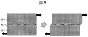
- Example 15 having a film laminated portion 12 having an interface layer 5 containing a large amount of metal elements having a small aggregation energy and Comparative Example 5 having a single-layer film 11 having no interface layer 5 introduced have resistance to resistance. It can be seen that the wear state of the surface after the wear test is different. As a result of observing the location where the surface peeling occurred, in Example 15 (FIG. 12), the peeled portion was uniformly extended laterally with respect to the sliding surface 70, and cracks did not grow so much in the film laminated portion 12. There was found.
Landscapes
- Chemical & Material Sciences (AREA)
- Organic Chemistry (AREA)
- Engineering & Computer Science (AREA)
- Chemical Kinetics & Catalysis (AREA)
- Materials Engineering (AREA)
- Metallurgy (AREA)
- Electrochemistry (AREA)
- General Chemical & Material Sciences (AREA)
- Mechanical Engineering (AREA)
- Crystallography & Structural Chemistry (AREA)
- Laminated Bodies (AREA)
- Electroplating Methods And Accessories (AREA)
- Electroplating And Plating Baths Therefor (AREA)
Priority Applications (3)
| Application Number | Priority Date | Filing Date | Title |
|---|---|---|---|
| EP20929210.1A EP4130346A4 (en) | 2020-03-31 | 2020-10-07 | Laminate, metal plating liquid, and laminate manufacturing method |
| US17/915,409 US12371792B2 (en) | 2020-03-31 | 2020-10-07 | Laminate, metal plating solution, and manufacturing process of laminate |
| CN202080099280.XA CN115362060B (zh) | 2020-03-31 | 2020-10-07 | 叠层体、金属镀敷液和叠层体的制造方法 |
Applications Claiming Priority (2)
| Application Number | Priority Date | Filing Date | Title |
|---|---|---|---|
| JP2020-061864 | 2020-03-31 | ||
| JP2020061864A JP7520550B2 (ja) | 2020-03-31 | 2020-03-31 | 積層体、金属めっき液、および積層体の製造方法 |
Publications (1)
| Publication Number | Publication Date |
|---|---|
| WO2021199468A1 true WO2021199468A1 (ja) | 2021-10-07 |
Family
ID=77927150
Family Applications (1)
| Application Number | Title | Priority Date | Filing Date |
|---|---|---|---|
| PCT/JP2020/038064 Ceased WO2021199468A1 (ja) | 2020-03-31 | 2020-10-07 | 積層体、金属めっき液、および積層体の製造方法 |
Country Status (5)
| Country | Link |
|---|---|
| US (1) | US12371792B2 (https=) |
| EP (1) | EP4130346A4 (https=) |
| JP (1) | JP7520550B2 (https=) |
| CN (1) | CN115362060B (https=) |
| WO (1) | WO2021199468A1 (https=) |
Families Citing this family (1)
| Publication number | Priority date | Publication date | Assignee | Title |
|---|---|---|---|---|
| WO2024202237A1 (ja) * | 2023-03-30 | 2024-10-03 | Jx金属株式会社 | 金属材料及び摺動部品 |
Citations (8)
| Publication number | Priority date | Publication date | Assignee | Title |
|---|---|---|---|---|
| JPS5377840A (en) * | 1976-12-21 | 1978-07-10 | Mishima Kosan Co Ltd | Preparation of mold for slab |
| JPS63105990A (ja) | 1986-10-23 | 1988-05-11 | Kawasaki Steel Corp | 多層ニツケル合金めつきおよびその形成方法 |
| JP2002180297A (ja) * | 2000-12-20 | 2002-06-26 | Honda Motor Co Ltd | Ni−Cu合金複合メッキ液 |
| JP2002180284A (ja) * | 2000-12-20 | 2002-06-26 | Honda Motor Co Ltd | Ni−Cu合金メッキ被膜 |
| JP2014082350A (ja) * | 2012-10-17 | 2014-05-08 | Takamatsu Mekki:Kk | Led用ウエハおよびその製造方法 |
| WO2016178372A1 (ja) * | 2015-05-07 | 2016-11-10 | 株式会社日立製作所 | 耐食皮膜を有する積層体とその製造方法 |
| JP2017196657A (ja) * | 2016-04-30 | 2017-11-02 | 新日鐵住金株式会社 | 鋳型の再生方法 |
| WO2019064672A1 (ja) | 2017-09-27 | 2019-04-04 | 株式会社日立製作所 | 皮膜積層体及びその製造方法 |
Family Cites Families (16)
| Publication number | Priority date | Publication date | Assignee | Title |
|---|---|---|---|---|
| US3288574A (en) * | 1964-04-10 | 1966-11-29 | Harshaw Chem Corp | Metal laminates and method of forming by electroplating |
| US3480522A (en) | 1966-08-18 | 1969-11-25 | Ibm | Method of making magnetic thin film device |
| US5171417A (en) * | 1989-09-13 | 1992-12-15 | Gould Inc. | Copper foils for printed circuit board applications and procedures and electrolyte bath solutions for electrodepositing the same |
| EP1461478B1 (en) * | 2000-12-20 | 2011-02-09 | Honda Giken Kogyo Kabushiki Kaisha | Composite plating film and a process for forming the same |
| KR100735481B1 (ko) * | 2005-12-09 | 2007-07-03 | 동부일렉트로닉스 주식회사 | 구리 배선 구조 및 그 형성 방법 |
| CA2730229C (en) * | 2008-07-07 | 2017-02-14 | John D. Whitaker | Property modulated materials and methods of making the same |
| BRPI1010877B1 (pt) * | 2009-06-08 | 2020-09-15 | Modumetal, Inc | Revestimento de multicamadas resistente à corrosão e método de eletrodeposição |
| RU2524937C1 (ru) * | 2010-09-02 | 2014-08-10 | Ниппон Стил Энд Сумитомо Метал Корпорейшн | Металлический лист c предварительно нанесённым покрытием с превосходной проводимостью и коррозионной стойкостью |
| JP5086485B1 (ja) * | 2011-09-20 | 2012-11-28 | Jx日鉱日石金属株式会社 | 電子部品用金属材料及びその製造方法 |
| WO2015198914A1 (ja) * | 2014-06-23 | 2015-12-30 | 奥野製薬工業株式会社 | 多層めっき皮膜及び該多層めっき皮膜を有する物品 |
| TWI593548B (zh) * | 2015-01-09 | 2017-08-01 | Jx日鑛日石金屬股份有限公司 | Attached to the metal substrate |
| CN104985392B (zh) * | 2015-05-11 | 2017-03-29 | 成都翱岳钣金制造有限公司 | 金属板材覆膜成型的工艺方法 |
| US10596636B2 (en) * | 2015-08-03 | 2020-03-24 | Tungaloy Corporation | Coated cutting tool |
| KR101693514B1 (ko) * | 2015-12-24 | 2017-01-06 | 주식회사 포스코 | 전기강판용 Fe-Ni-P 합금 다층 강판 및 이의 제조방법 |
| WO2018189901A1 (ja) * | 2017-04-14 | 2018-10-18 | Ykk株式会社 | めっき材及びその製造方法 |
| JP7121881B2 (ja) * | 2017-08-08 | 2022-08-19 | 三菱マテリアル株式会社 | 銀皮膜付端子材及び銀皮膜付端子 |
-
2020
- 2020-03-31 JP JP2020061864A patent/JP7520550B2/ja active Active
- 2020-10-07 WO PCT/JP2020/038064 patent/WO2021199468A1/ja not_active Ceased
- 2020-10-07 CN CN202080099280.XA patent/CN115362060B/zh active Active
- 2020-10-07 US US17/915,409 patent/US12371792B2/en active Active
- 2020-10-07 EP EP20929210.1A patent/EP4130346A4/en active Pending
Patent Citations (8)
| Publication number | Priority date | Publication date | Assignee | Title |
|---|---|---|---|---|
| JPS5377840A (en) * | 1976-12-21 | 1978-07-10 | Mishima Kosan Co Ltd | Preparation of mold for slab |
| JPS63105990A (ja) | 1986-10-23 | 1988-05-11 | Kawasaki Steel Corp | 多層ニツケル合金めつきおよびその形成方法 |
| JP2002180297A (ja) * | 2000-12-20 | 2002-06-26 | Honda Motor Co Ltd | Ni−Cu合金複合メッキ液 |
| JP2002180284A (ja) * | 2000-12-20 | 2002-06-26 | Honda Motor Co Ltd | Ni−Cu合金メッキ被膜 |
| JP2014082350A (ja) * | 2012-10-17 | 2014-05-08 | Takamatsu Mekki:Kk | Led用ウエハおよびその製造方法 |
| WO2016178372A1 (ja) * | 2015-05-07 | 2016-11-10 | 株式会社日立製作所 | 耐食皮膜を有する積層体とその製造方法 |
| JP2017196657A (ja) * | 2016-04-30 | 2017-11-02 | 新日鐵住金株式会社 | 鋳型の再生方法 |
| WO2019064672A1 (ja) | 2017-09-27 | 2019-04-04 | 株式会社日立製作所 | 皮膜積層体及びその製造方法 |
Non-Patent Citations (4)
| Title |
|---|
| KITTEL: "Introduction to Solid State Physics", vol. 1, 1978, MARUZEN CO., LTD, pages: 70 |
| S.C. CHOWDHURYB.Z.G. HAQUEJ.W. GILESPIE, J. MATER. SCI., vol. 51, pages 10139 |
| See also references of EP4130346A4 |
| WATANABE, TOHRU: "Preparation of Multi Layer Film by Plating Method", HYOMEN KAGAKU, vol. 14, no. 9, 1993, pages 565 - 569, XP055965659 * |
Also Published As
| Publication number | Publication date |
|---|---|
| JP2021160117A (ja) | 2021-10-11 |
| EP4130346A4 (en) | 2023-12-20 |
| US12371792B2 (en) | 2025-07-29 |
| EP4130346A1 (en) | 2023-02-08 |
| CN115362060A (zh) | 2022-11-18 |
| JP7520550B2 (ja) | 2024-07-23 |
| CN115362060B (zh) | 2024-06-18 |
| US20230143193A1 (en) | 2023-05-11 |
Similar Documents
| Publication | Publication Date | Title |
|---|---|---|
| Hu et al. | Deposition process and properties of electroless Ni-P-Al2O3 composite coatings on magnesium alloy | |
| Gül et al. | Characteristics of electro-co-deposited Ni–Al2O3 nano-particle reinforced metal matrix composite (MMC) coatings | |
| Ünal et al. | Production and characterization of electrodeposited Ni-B/hBN composite coatings | |
| Popoola et al. | Surface characterization, mechanical properties and corrosion behaviour of ternary based Zn–ZnO–SiO2composite coating of mild steel | |
| Dilek et al. | Pulse electro co-deposition of submicron-sized TiC reinforced Ni–W coatings: Tribological and corrosion properties | |
| Matsui et al. | Electrodeposition with intermittent addition of trimethylamine borane to produce ductile bulk nanocrystalline Ni–B alloys | |
| TWI276706B (en) | Iron-phosphorus electroplating bath and method | |
| US11866830B2 (en) | Abrasive tip coating | |
| Mahdavi et al. | Characteristics and properties of Cr coatings electrodeposited from Cr (III) baths | |
| Sheu et al. | Effects of alumina addition and heat treatment on the behavior of Cr coatings electroplated from a trivalent chromium bath | |
| Hussain et al. | Recent developments in graphene based metal matrix composite coatings for corrosion protection application: A review | |
| Rahman et al. | A review of the tribological behavior of electrodeposited cobalt (Co) based composite coatings | |
| Xu et al. | Preparation of nanocrystalline Ni–Mo and Ni–Mo–ZrO2 coating and investigation of its corrosion resistance and wear behaviors | |
| US20090223829A1 (en) | Micro-Arc Assisted Electroless Plating Methods | |
| Matsui et al. | Improvement in tensile ductility of electrodeposited bulk nanocrystalline Ni–W by sulfamate bath using propionic acid | |
| Xu et al. | Enhancement of wear and corrosion resistance of pulsed electrodeposited Ni–Mo amorphous/nanocrystalline coatings by heat treatment | |
| KR102043505B1 (ko) | 강판용 전기 도금액 및 이를 이용한 강판의 전기 도금 방법 | |
| WO2021199468A1 (ja) | 積層体、金属めっき液、および積層体の製造方法 | |
| Shinohara et al. | An effective strategy for improving the performance of electrodeposited Fe-W alloy plating: Tailoring microstructure by graphene incorporation | |
| Faride et al. | Characterization of Nano-Crystalline NiP Alloy Coatings Electrodeposited at Various Current Densities. | |
| Matallana Guerrero et al. | Electrochemical performance of γ-Ni2Zn11 coatings synthesized from non-aqueous bath | |
| Akarapu et al. | Surface property modification of copper by nanocomposite coating | |
| CN110799670A (zh) | 防锈构件及其制造方法 | |
| Mahdavi et al. | Enhanced corrosion resistance of cobalt coatings: the role of ZrB2 particle incorporation | |
| JP6813692B2 (ja) | 皮膜積層体及びその製造方法 |
Legal Events
| Date | Code | Title | Description |
|---|---|---|---|
| 121 | Ep: the epo has been informed by wipo that ep was designated in this application |
Ref document number: 20929210 Country of ref document: EP Kind code of ref document: A1 |
|
| NENP | Non-entry into the national phase |
Ref country code: DE |
|
| ENP | Entry into the national phase |
Ref document number: 2020929210 Country of ref document: EP Effective date: 20221031 |
|
| WWG | Wipo information: grant in national office |
Ref document number: 17915409 Country of ref document: US |