WO2021193357A1 - 熱電変換モジュール - Google Patents
熱電変換モジュール Download PDFInfo
- Publication number
- WO2021193357A1 WO2021193357A1 PCT/JP2021/011109 JP2021011109W WO2021193357A1 WO 2021193357 A1 WO2021193357 A1 WO 2021193357A1 JP 2021011109 W JP2021011109 W JP 2021011109W WO 2021193357 A1 WO2021193357 A1 WO 2021193357A1
- Authority
- WO
- WIPO (PCT)
- Prior art keywords
- thermoelectric conversion
- thermoelectric
- conversion material
- material layer
- thermoelectric semiconductor
- Prior art date
- Legal status (The legal status is an assumption and is not a legal conclusion. Google has not performed a legal analysis and makes no representation as to the accuracy of the status listed.)
- Ceased
Links
Images




Classifications
-
- H—ELECTRICITY
- H10—SEMICONDUCTOR DEVICES; ELECTRIC SOLID-STATE DEVICES NOT OTHERWISE PROVIDED FOR
- H10N—ELECTRIC SOLID-STATE DEVICES NOT OTHERWISE PROVIDED FOR
- H10N10/00—Thermoelectric devices comprising a junction of dissimilar materials, i.e. devices exhibiting Seebeck or Peltier effects
- H10N10/80—Constructional details
- H10N10/85—Thermoelectric active materials
- H10N10/857—Thermoelectric active materials comprising compositions changing continuously or discontinuously inside the material
-
- H—ELECTRICITY
- H10—SEMICONDUCTOR DEVICES; ELECTRIC SOLID-STATE DEVICES NOT OTHERWISE PROVIDED FOR
- H10N—ELECTRIC SOLID-STATE DEVICES NOT OTHERWISE PROVIDED FOR
- H10N10/00—Thermoelectric devices comprising a junction of dissimilar materials, i.e. devices exhibiting Seebeck or Peltier effects
- H10N10/01—Manufacture or treatment
-
- H—ELECTRICITY
- H10—SEMICONDUCTOR DEVICES; ELECTRIC SOLID-STATE DEVICES NOT OTHERWISE PROVIDED FOR
- H10N—ELECTRIC SOLID-STATE DEVICES NOT OTHERWISE PROVIDED FOR
- H10N10/00—Thermoelectric devices comprising a junction of dissimilar materials, i.e. devices exhibiting Seebeck or Peltier effects
- H10N10/10—Thermoelectric devices comprising a junction of dissimilar materials, i.e. devices exhibiting Seebeck or Peltier effects operating with only the Peltier or Seebeck effects
- H10N10/17—Thermoelectric devices comprising a junction of dissimilar materials, i.e. devices exhibiting Seebeck or Peltier effects operating with only the Peltier or Seebeck effects characterised by the structure or configuration of the cell or thermocouple forming the device
-
- H—ELECTRICITY
- H10—SEMICONDUCTOR DEVICES; ELECTRIC SOLID-STATE DEVICES NOT OTHERWISE PROVIDED FOR
- H10N—ELECTRIC SOLID-STATE DEVICES NOT OTHERWISE PROVIDED FOR
- H10N10/00—Thermoelectric devices comprising a junction of dissimilar materials, i.e. devices exhibiting Seebeck or Peltier effects
- H10N10/80—Constructional details
- H10N10/85—Thermoelectric active materials
- H10N10/851—Thermoelectric active materials comprising inorganic compositions
- H10N10/852—Thermoelectric active materials comprising inorganic compositions comprising tellurium, selenium or sulfur
-
- H—ELECTRICITY
- H10—SEMICONDUCTOR DEVICES; ELECTRIC SOLID-STATE DEVICES NOT OTHERWISE PROVIDED FOR
- H10N—ELECTRIC SOLID-STATE DEVICES NOT OTHERWISE PROVIDED FOR
- H10N10/00—Thermoelectric devices comprising a junction of dissimilar materials, i.e. devices exhibiting Seebeck or Peltier effects
- H10N10/80—Constructional details
- H10N10/85—Thermoelectric active materials
- H10N10/851—Thermoelectric active materials comprising inorganic compositions
- H10N10/855—Thermoelectric active materials comprising inorganic compositions comprising compounds containing boron, carbon, oxygen or nitrogen
Definitions
- the present invention relates to a thermoelectric conversion module.
- thermoelectric conversion module a configuration of a so-called ⁇ -type thermoelectric conversion element is known.
- the ⁇ -type thermoelectric conversion element is provided with a pair of electrodes separated from each other on the substrate, for example, a P-type thermoelectric element is provided on one of the electrodes, and an N-type thermoelectric element is provided on the other electrode. It is provided so as to be separated from each other, and the upper surfaces of both thermoelectric elements are connected to the electrodes of the opposing substrates.
- thermoelectric conversion element a so-called in-plane type thermoelectric conversion element.
- inplane type thermoelectric conversion element P-type thermoelectric elements and N-type thermoelectric elements are alternately provided in the in-plane direction of the substrate.
- the lower part of the joint between the two thermoelectric elements is connected in series via an electrode. It is composed of.
- a resin substrate such as polyimide is used as a substrate used for a thermoelectric conversion module from the viewpoint of heat resistance and flexibility.
- thermoelectric semiconductor material As the N-type thermoelectric semiconductor material and the P-type thermoelectric semiconductor material, a thin film of a bismuthtellide-based material is used from the viewpoint of thermoelectric performance. For example, from the viewpoint of flexibility and thinning, a resin and a thermoelectric semiconductor material are used.
- the thermoelectric semiconductor composition containing the above is formed in the form of a coating film by using a screen printing method or the like. (See, for example, Patent Document 1).
- thermoelectric conversion module could not sufficiently reduce the electrical resistivity of the thermoelectric conversion material in the thermoelectric conversion material layer, and the thermoelectric performance was not sufficient.
- thermoelectric conversion module having a thermoelectric conversion material layer having high thermoelectric performance in which the electrical resistivity of the thermoelectric conversion material in the thermoelectric conversion material layer is reduced.
- thermoelectric conversion material layer in the thermoelectric conversion module has voids, and the thermoelectric conversion material has a vertical cross-sectional area including the central portion of the thermoelectric conversion material layer.
- the filling rate is more than 0.900 and less than 1.000, the electrical resistivity of the thermoelectric conversion material in the thermoelectric conversion material layer is reduced, and the thermoelectric conversion material layer is used. It was found that the thermoelectric performance of the module can be improved.
- the present inventors have found that by using a thermoelectric semiconductor composition containing a resin binder that decomposes at a low temperature, voids in the thermoelectric conversion material layer can be reduced and the filling rate can be improved. completed.
- thermoelectric conversion module having a thermoelectric conversion material layer made of a thermoelectric conversion material containing at least thermoelectric semiconductor particles, wherein the thermoelectric conversion material layer has voids and a vertical cross section including a central portion of the thermoelectric conversion material layer.
- a thermoelectric conversion module having a filling rate of more than 0.900 and less than 1.000, where the filling rate is defined as the ratio of the area of the thermoelectric conversion material to the area of.
- thermoelectric conversion module according to (2) above wherein the binder resin is decomposed by 90% by mass or more at the firing temperature of the fired body.
- the binder resin contains at least one selected from polycarbonate, a cellulose derivative and a polyvinyl polymer.
- the thermoelectric conversion module according to any one of (2) to (5) above, wherein the thermoelectric semiconductor composition further contains an ionic liquid and / or an inorganic ionic compound.
- thermoelectric semiconductor particles are made of a bismuth-tellurium-based thermoelectric semiconductor material, a tellurium-based thermoelectric semiconductor material, an antimony-tellurium-based thermoelectric semiconductor material, or a bismuth selenide-based thermoelectric semiconductor material.
- thermoelectric conversion module having a thermoelectric conversion material layer having high thermoelectric performance in which the electrical resistivity of the thermoelectric conversion material in the thermoelectric conversion material layer is reduced.
- thermoelectric conversion module of this invention It is a figure for demonstrating the definition of the vertical cross section of the thermoelectric conversion material layer in the thermoelectric conversion module of this invention. It is sectional drawing for demonstrating the vertical cross section of the thermoelectric conversion material layer in the thermoelectric conversion module of this invention. It is explanatory drawing explaining an example of the manufacturing method of the thermoelectric conversion material layer (chip) used for manufacturing the thermoelectric conversion module of this invention. It is explanatory drawing explaining an example of the method of manufacturing the thermoelectric conversion module of this invention. 6 is an SEM image of a vertical cross section of the test piece (thermoelectric conversion material layer) of Example 1. 6 is an SEM image of a vertical cross section of the test piece (thermoelectric conversion material layer) of Comparative Example 1.
- thermoelectric conversion module has at least a thermoelectric conversion material layer, and if necessary, an electrode, a resin film, a bonding material layer, and a solder receiving layer described in the column of "Manufacturing method of thermoelectric conversion module" described later. , Etc. are further included.
- a chip made of a P-type thermoelectric conversion material and a chip made of an N-type thermoelectric conversion material as a thermoelectric conversion material layer are interposed with electrodes so as to form a ⁇ -type or in-plane type thermoelectric conversion module. It is preferable to place (arrange) and manufacture the components so that they are connected to each other.
- thermoelectric conversion material layer is made of a thermoelectric conversion material, has voids, and is described later when the filling rate is the ratio of the area of the thermoelectric conversion material to the area of the longitudinal section including the central portion of the thermoelectric conversion material layer.
- the filling factor measured by the example method is greater than 0.900 and less than 1.000.
- a "thermoelectric conversion material” means the thing which fired the thermoelectric semiconductor composition (for example, the fired body of the coating film of a thermoelectric semiconductor composition). Even if the thermoelectric semiconductor composition contains a binder resin described later, if the binder resin is completely decomposed by firing, the thermoelectric conversion material does not contain the binder resin.
- FIG. 1 is a diagram for explaining the definition of a vertical cross section of a thermoelectric conversion material layer in the thermoelectric conversion module of the present invention
- FIG. 1A is a plan view of the thermoelectric conversion material layer 20 and is a thermoelectric conversion material.
- the layer 20 has a length X in the width direction and a length Y in the depth direction
- FIG. 1B is a vertical cross section of the thermoelectric conversion material layer 20 formed on the substrate 1a. It includes the central portion C in FIG. 1A, and is composed of a length X and a thickness D obtained when cutting between A and A'in the width direction (rectangular in the figure).
- the thermoelectric conversion material layer 20 includes a void portion 30.
- FIG. 2 is a schematic cross-sectional view for explaining a vertical cross section of the thermoelectric conversion material layer in the thermoelectric conversion module of the present invention
- FIG. 2A is a vertical cross section of the thermoelectric conversion material layer 20s formed on the substrate 1a.
- the thermoelectric conversion material layer 20s has a vertical cross section consisting of a curve having a length X in the width direction and Dmin and Dmax values in the thickness direction, and the upper part of the vertical cross section has a concave portion and a convex portion. 30b is present in the vertical cross section.
- FIG. 2 is a schematic cross-sectional view for explaining a vertical cross section of the thermoelectric conversion material layer in the thermoelectric conversion module of the present invention
- FIG. 2A is a vertical cross section of the thermoelectric conversion material layer 20s formed on the substrate 1a.
- the thermoelectric conversion material layer 20s has a vertical cross section consisting of a curve having a length X in the width direction and Dmin and Dmax values in the thickness direction, and the
- thermoelectric conversion material layer 20t is an example of a vertical cross section of the thermoelectric conversion material layer 20t formed on the substrate 1a, and the vertical cross section of the thermoelectric conversion material layer 20t has a length X in the width direction and a thickness in the thickness direction.
- the length is D [when the values of Dmin and Dmax in (a) of FIG. 2 are small], the upper part of the vertical cross section is substantially linear, and the number of voids and the volume are contained in the vertical cross section. There is a suppressed void 40b.
- Dmin means the minimum value of the thickness in the thickness direction of the vertical cross section
- Dmax means the maximum value of the thickness in the thickness direction of the vertical cross section.
- thermoelectric conversion material in the thermoelectric conversion material layer is defined by the ratio of the area of the thermoelectric conversion material to the area of the longitudinal section including the central portion of the thermoelectric conversion material layer.
- the filling rate is more than 0.900 and less than 1.000, and there are few voids in the thermoelectric conversion material layer.
- the filling rate of the thermoelectric conversion material in the thermoelectric conversion material layer is 0.900 or less, the voids in the thermoelectric conversion material layer increase, and it is difficult to reduce the electrical resistivity of the thermoelectric conversion material in the thermoelectric conversion material layer (excellent). It becomes difficult to obtain electrical conductivity), and high thermoelectric performance cannot be obtained.
- the filling rate is preferably more than 0.900 and 0.999 or less, more preferably 0.920 or more and 0.999 or less, still more preferably 0.950 or more and 0.999 or less, and particularly preferably 0.970 or more and 0.999 or less.
- the filling rate of the thermoelectric conversion material in the thermoelectric conversion material layer was measured by the method described in the examples.
- thermoelectric conversion material layer in the thermoelectric conversion module of the present invention is preferably made of a fired body of a coating film of a thermoelectric semiconductor composition.
- the thermoelectric semiconductor composition preferably contains at least thermoelectric semiconductor particles and further contains a binder resin from the viewpoint of shape stability of the thermoelectric conversion material layer, and is ionic liquid and inorganic ionic from the viewpoint of thermoelectric performance of the thermoelectric conversion material layer. More preferably, it further comprises at least one of the compounds.
- the fired body is obtained by firing the coating film of the thermoelectric semiconductor composition at the firing temperature.
- the firing temperature is usually determined by the type of thermoelectric semiconductor particles contained in the thermoelectric semiconductor composition, and is usually 260 to 500 ° C, preferably 400 to 460 ° C, more preferably 410 to 450 ° C, and particularly preferably. It is 420 to 450 ° C. In the example, the firing temperature is 430 ° C.
- the thickness of the thermoelectric conversion material layer is not particularly limited, but is preferably 1 nm to 1000 ⁇ m, more preferably 3 to 600 ⁇ m, and further preferably 5 to 400 ⁇ m from the viewpoint of flexibility, thermoelectric performance, and film strength.
- thermoelectric semiconductor particles are obtained by pulverizing a thermoelectric semiconductor material, which will be described later, to a predetermined size by a fine pulverizer or the like.
- the thermoelectric semiconductor material is not particularly limited as long as it is a material capable of generating thermoelectromotive force by imparting a temperature difference.
- thermoelectric semiconductor materials such as Bi 2 Se 3 ; VDD thermoelectric semiconductor materials such as ⁇ -FeSi 2 , CrSi 2 , MnSi 1.73 , Mg 2 Si; Oxide thermoelectric semiconductor materials; Whistler materials such as FeVAL, FeVALSi, and FeVTiAl; sulfide-based thermoelectric semiconductor materials such as TiS 2; and the like are used.
- VDD thermoelectric semiconductor materials such as ⁇ -FeSi 2 , CrSi 2 , MnSi 1.73 , Mg 2 Si
- Oxide thermoelectric semiconductor materials such as FeVAL, FeVALSi, and FeVTiAl
- sulfide-based thermoelectric semiconductor materials such as TiS 2; and the like are used.
- One of these may be used alone, or two or more thereof may be used in combination.
- thermoelectric semiconductor materials such as type bismuth sterlide are more preferable.
- the P-type bismuth telluride one having a hole as a carrier and a positive Seebeck coefficient, for example, represented by Bi X Te 3 Sb 2-X is preferably used.
- X is preferably 0 ⁇ X ⁇ 0.8, more preferably 0.4 ⁇ X ⁇ 0.6.
- the Seebeck coefficient and the electric conductivity become large, and the characteristics as a P-type thermoelectric element are maintained, which is preferable.
- the N-type bismuth telluride those having an electron carrier and a negative Seebeck coefficient, for example, represented by Bi 2 Te 3-Y Se Y , are preferably used.
- Y is 0 or more and 3 or less, the Seebeck coefficient and the electric conductivity become large, and the characteristics as an N-type thermoelectric element are maintained, which is preferable.
- the content of the thermoelectric semiconductor particles in the thermoelectric semiconductor composition is preferably 30 to 99% by mass, more preferably 50 to 96% by mass, and particularly preferably 70 to 95% by mass.
- the Seebeck coefficient absolute value of the Perche coefficient
- the decrease in the electric conductivity is suppressed, and only the thermal conductivity is decreased, so that high thermoelectric performance is exhibited.
- a film having sufficient film strength and flexibility can be obtained, which is preferable.
- the content of the thermoelectric semiconductor particles in the thermoelectric conversion material is preferably 80 to 100% by mass, more preferably 90 to 100% by mass, further preferably 95 to 100% by mass, and particularly preferably 99 to 100% by mass. Most preferably, it is 99.9 to 100% by mass.
- the Seebeck coefficient absolute value of the Perche coefficient
- the decrease in the electric conductivity is suppressed, and only the thermal conductivity is decreased. It is preferable to obtain a film having high thermoelectric performance, sufficient film strength, and appropriate flexibility.
- the average particle size of the thermoelectric semiconductor particles is preferably 10 nm to 200 ⁇ m, more preferably 10 nm to 30 ⁇ m, still more preferably 50 nm to 10 ⁇ m, and particularly preferably 1 to 6 ⁇ m. Within the above range, uniform dispersion can be facilitated and the electrical conductivity can be increased.
- the method of pulverizing the thermoelectric semiconductor material to obtain thermoelectric semiconductor particles is not particularly limited, and may be pulverized to a predetermined size by a known fine pulverizer such as a jet mill, a ball mill, a bead mill, a colloid mill, a roller mill or the like. ..
- the average particle size of the thermoelectric semiconductor particles was obtained by measuring with a laser diffraction type particle size analyzer (Mastersizer 3000 manufactured by Malvern), and was used as the median value of the particle size distribution.
- thermoelectric semiconductor particles are preferably those that have been heat-treated in advance.
- the heat treatment is not particularly limited, but before preparing the thermoelectric semiconductor composition, the gas flow rate is controlled so as not to adversely affect the thermoelectric semiconductor particles under an atmosphere of an inert gas such as nitrogen or argon. It is preferably carried out in a reducing gas atmosphere such as hydrogen or under vacuum conditions, and more preferably in a mixed gas atmosphere of an inert gas and a reducing gas.
- the specific temperature condition depends on the thermoelectric semiconductor particles used, but it is usually preferable to carry out the temperature at a temperature equal to or lower than the melting point of the particles and at 100 to 1500 ° C. for several minutes to several tens of hours.
- the thermoelectric semiconductor composition preferably contains a binder resin in addition to the thermoelectric semiconductor particles described above.
- the binder resin facilitates peeling from the substrate used for producing the chip of the thermoelectric conversion material after the firing (annealing) treatment, and also acts as a binder between the thermoelectric semiconductor materials (thermoelectric semiconductor particles), and serves as a binder for the thermoelectric conversion module. Flexibility can be enhanced, and the formation of a thin film by coating or the like is facilitated.
- the binder resin is preferably a resin that decomposes in an amount of 90% by mass or more at the firing (annealing) temperature, more preferably a resin that decomposes in an amount of 95% by mass or more, and a resin that decomposes in an amount of 99% by mass or more. It is particularly preferable to have. Further, when a coating film (thin film) made of a thermoelectric semiconductor composition is crystal-grown into thermoelectric semiconductor particles by firing (annealing) treatment or the like, a resin that maintains various physical properties such as mechanical strength and thermal conductivity without being impaired. More preferred.
- the binder resin If a resin that decomposes by 90% by mass or more at the firing (annealing) temperature, that is, a resin that decomposes at a lower temperature than the heat-resistant resin conventionally used, is used as the binder resin, the binder resin is decomposed by firing. Since the content of the binder resin, which is an insulating component contained in the fired body, is reduced and the crystal growth of the thermoelectric semiconductor particles in the thermoelectric semiconductor composition is promoted, the voids in the thermoelectric conversion material layer are reduced and filled. The rate can be improved.
- Whether or not the resin decomposes at a predetermined value (for example, 90% by mass) or more at the firing (annealing) temperature is determined by the mass reduction rate (mass before decomposition) at the firing (annealing) temperature by thermogravimetric analysis (TG). Judgment is made by measuring (value obtained by dividing the mass after decomposition).
- a predetermined value for example, 90% by mass
- TG thermogravimetric analysis
- thermoplastic resin examples include polyolefin resins such as polyethylene, polypropylene, polyisobutylene, and polymethylpentene; polycarbonate; thermoplastic polyester resins such as polyethylene terephthalate and polyethylene naphthalate; polystyrene, acrylonitrile-styrene copolymer, and polyacetic acid.
- Examples thereof include vinyl, ethylene-vinyl acetate copolymer, polyvinyl chloride, polyvinylpyridine, polyvinyl alcohol, polyvinyl polymer such as polyvinylpyrrolidone; polyurethane; cellulose derivative such as ethyl cellulose; and the like.
- Examples of the curable resin include thermosetting resins and photocurable resins.
- examples of the thermosetting resin include epoxy resin and phenol resin.
- Examples of the photocurable resin include a photocurable acrylic resin, a photocurable urethane resin, and a photocurable epoxy resin. One of these may be used alone, or two or more thereof may be used in combination.
- thermoplastic resin a thermoplastic resin is preferable, a cellulose derivative such as polycarbonate and ethyl cellulose is more preferable, and polycarbonate is particularly preferable.
- the binder resin is appropriately selected according to the temperature of the firing (annealing) treatment of the thermoelectric semiconductor material in the (B) firing (annealing) treatment step described later. It is preferable to perform the firing (annealing) treatment at a temperature equal to or higher than the final decomposition temperature of the binder resin from the viewpoint of the electrical resistivity of the thermoelectric conversion material in the thermoelectric conversion material layer.
- the "final decomposition temperature” is a temperature at which the mass reduction rate at the firing (annealing) temperature by thermogravimetric analysis (TG) is 100% (the mass after decomposition is 0% of the mass before decomposition). say.
- the final decomposition temperature of the binder resin is usually 150 to 600 ° C., preferably 200 to 560 ° C., more preferably 220 to 460 ° C., and particularly preferably 240 to 360 ° C. If a binder resin having a final decomposition temperature in this range is used, it functions as a binder for the thermoelectric semiconductor material, and a thin film can be easily formed during printing.
- the content of the binder resin in the thermoelectric semiconductor composition is 0.1 to 40% by mass, preferably 0.5 to 20% by mass, more preferably 0.5 to 10% by mass, and particularly preferably 0.5 to 5%. It is mass%.
- the content of the binder resin is within the above range, the electrical resistivity of the thermoelectric conversion material in the thermoelectric conversion material layer can be reduced.
- the content of the binder resin in the thermoelectric conversion material is preferably 0 to 10% by mass, more preferably 0 to 5% by mass, and particularly preferably 0 to 1% by mass.
- the electrical resistivity of the thermoelectric conversion material in the thermoelectric conversion material layer can be reduced.
- An ionic liquid is a molten salt formed by combining a cation and an anion, and refers to a salt that can exist as a liquid in any temperature range of ⁇ 50 ° C. or higher and lower than 400 ° C.
- Ionic liquids have features such as extremely low vapor pressure, non-volatility, excellent thermostability and electrochemical stability, low viscosity, and high ionic conductivity. Therefore, as a conductive auxiliary agent, it is possible to effectively suppress the reduction of the electrical conductivity between the thermoelectric semiconductor particles. Further, since the ionic liquid exhibits high polarity based on the aprotic ionic structure and has excellent compatibility with the binder resin, the electric conductivity of the chip of the thermoelectric conversion material can be made uniform.
- the ionic liquid include, for example, (1) nitrogen-containing cyclic cation compounds such as pyridinium, pyrimidinium, pyrazolium, pyrrolidinium, piperidinium, and imidazolium and derivatives thereof; amine-based cations of tetraalkylammonium and derivatives thereof; phosphonium and trialkylsulfonium.
- nitrogen-containing cyclic cation compounds such as pyridinium, pyrimidinium, pyrazolium, pyrrolidinium, piperidinium, and imidazolium and derivatives thereof
- amine-based cations of tetraalkylammonium and derivatives thereof such as phosphonium and trialkylsulfonium.
- phosphine cations and derivatives thereof such as tetraalkylphosphonium; lithium cations and derivatives thereof; and a cationic component such as, (2) Cl -, AlCl 4 -, Al 2 Cl 7 -, ClO 4 - chloride such as ion ; like iodide ion; - - I; BF 4 - , PF 6 - fluoride ions such; Br etc.
- F (HF) n - halides such anions; NO 3 -, CH 3 COO -, CF 3 COO -, CH 3 SO 3 -, CF 3 SO 3 -, (FSO 2) 2 N -, (CF 3 SO 2) 2 N -, (CF 3 SO 2) 3 C -, AsF 6 -, SbF 6 -, NbF 6 -, TaF 6 -, F (HF) n -, (CN) 2 n -, C 4 F 9 SO 3 -, (C 2 F 5 SO 2) 2 n -, C 3 F 7 COO -, (CF 3 SO 2) (CF 3 CO) N -; include those composed of an anion component such as. One of these may be used alone, or two or more thereof may be used in combination.
- the cation component of the ionic liquid is pyridinium cation and its It preferably contains at least one selected from derivatives, imidazolium cations and derivatives thereof.
- the anion component of the ionic liquid preferably contains a halide anion, and more preferably contains at least one selected from Cl ⁇ , Br ⁇ and I ⁇ .
- ionic liquids in which the cation component contains a pyridinium cation and a derivative thereof include 4-methyl-butylpyridinium chloride, 3-methyl-butylpyridinium chloride, 4-methyl-hexylpyridinium chloride, and 3-methyl-hexylpyridinium.
- Chloride 4-methyl-octylpyridinium chloride, 3-methyl-octylpyridinium chloride, 3,4-dimethyl-butylpyridinium chloride, 3,5-dimethyl-butylpyridinium chloride, 4-methyl-butylpyridiniumtetrafluoroborate, 4- Methyl-butylpyridinium hexafluorophosphate, 1-butylpyridinium bromide, 1-butyl-4-methylpyridinium bromide, 1-butyl-4-methylpyridinium hexafluorophosphate, 1-butyl-4-methylpyridinium iodide, etc. Be done.
- 1-butylpyridinium bromide 1-butyl-4-methylpyridinium bromide, 1-butyl-4-methylpyridinium hexafluorophosphate, and 1-butyl-4-methylpyridinium iodide are preferable.
- the ionic liquid in which the cation component contains an imidazolium cation and a derivative thereof [1-butyl-3- (2-hydroxyethyl) imidazolium bromide] and [1-butyl-3- (2) -Hydroxyethyl) imidazolium tetrafluoroborate], 1-ethyl-3-methylimidazolium chloride, 1-ethyl-3-methylimidazolium bromide, 1-butyl-3-methylimidazolium chloride, 1-hexyl-3 -Methylimidazolium chloride, 1-octyl-3-methylimidazolium chloride, 1-decyl-3-methylimidazolium chloride, 1-decyl-3-methylimidazolium bromide, 1-dodecyl-3-methylimidazolium chloride, 1-Tetradecyl-3-methylimidazolium chloride, 1-ethyl-3- (2-hydroxyeth
- the electrical conductivity of the above ionic liquid is preferably 10-7 S / cm or more, more preferably 10-6 S / cm or more.
- the electric conductivity is in the above range, the reduction of the electric conductivity between the thermoelectric semiconductor particles can be effectively suppressed as a conductivity auxiliary agent.
- the above-mentioned ionic liquid preferably has a decomposition temperature of 300 ° C. or higher.
- the decomposition temperature means a temperature at which the mass reduction rate at the firing (annealing) temperature by thermogravimetric analysis (TG) is 10%.
- the mass reduction rate at 300 ° C. by thermogravimetric analysis (TG) is preferably 10% or less, more preferably 5% or less, and particularly preferably 1% or less. As long as the mass reduction rate is within the above range, the effect as a conductive auxiliary agent can be maintained even when the coating film (thin film) made of the thermoelectric semiconductor composition is fired (annealed) as described later.
- the content of the ionic liquid in the thermoelectric semiconductor composition is preferably 0.01 to 50% by mass, more preferably 0.5 to 30% by mass, and particularly preferably 1.0 to 20% by mass.
- the content of the ionic liquid is within the above range, the decrease in electrical conductivity is effectively suppressed, and a film having high thermoelectric performance can be obtained.
- the content of the ionic liquid in the thermoelectric conversion material is preferably 0.01 to 50% by mass, more preferably 0.5 to 30% by mass, and particularly preferably 1.0 to 20% by mass.
- the content of the ionic liquid in the thermoelectric conversion material is within the above range, the decrease in electrical conductivity is effectively suppressed, and a film having high thermoelectric performance can be obtained.
- Inorganic ionic compounds are compounds composed of at least cations and anions.
- the inorganic ionic compound is solid at room temperature, has a melting point in any temperature in the temperature range of 400 to 900 ° C., and has characteristics such as high ionic conductivity. Therefore, it can be used as a conductive auxiliary agent. It is possible to suppress a decrease in electrical conductivity between thermoelectric semiconductor particles.
- the content of the inorganic ionic compound in the thermoelectric semiconductor composition is preferably 0.01 to 50% by mass, more preferably 0.5 to 30% by mass, and particularly preferably. Is 1.0 to 10% by mass.
- the content of the inorganic ionic compound is within the above range, the decrease in electrical conductivity can be effectively suppressed, and as a result, a film having improved thermoelectric performance can be obtained.
- the total content of the inorganic ionic compound and the ionic liquid in the thermoelectric semiconductor composition is preferably 0.01 to 50% by mass, more preferably. Is 0.5 to 30% by mass, particularly preferably 1.0 to 10% by mass.
- the content of the inorganic ionic compound in the thermoelectric conversion material is preferably 0.01 to 50% by mass, more preferably 0.5 to 30% by mass, and particularly preferably 1.0 to 10% by mass.
- the content of the inorganic ionic compound in the thermoelectric conversion material is within the above range, the decrease in electrical conductivity can be effectively suppressed, and as a result, a film having improved thermoelectric performance can be obtained.
- thermoelectric semiconductor composition may further include a dispersant, a film-forming aid, a light stabilizer, an antioxidant, a tackifier, a plasticizer, a colorant, a resin stabilizer, a filler, and the like. It may contain other additives such as pigments, conductive fillers, conductive polymers and hardeners. One of these may be used alone, or two or more thereof may be used in combination.
- thermoelectric conversion module of the present invention includes the following steps (i) to (vii).
- thermoelectric conversion material layer (chip) A step of peeling the other surface of the thermoelectric conversion material layer (chip) after the step of (v) from the substrate; and (vi): A thermoelectric conversion material obtained by peeling in the step of (vi) above.
- the other surface of the layer (chip) and the electrode of the second layer prepared in the above step (iv) are joined via the second bonding material layer, or prepared in the above step (iv).
- thermoelectric conversion material layer (chip)
- a step of forming a coating film of a thermoelectric semiconductor composition on a substrate (B) A step of drying the coating film of the thermoelectric semiconductor composition obtained in the above step (A); (C) A step of peeling the coating film of the thermoelectric semiconductor composition after drying obtained in (B) above from the substrate; (D) A step of heat-pressing (heat-pressurizing) the coating film of the thermoelectric semiconductor composition obtained in (C) above; (E) The thermoelectric semiconductor composition after pressing obtained in the step (D) above. It includes a step of firing (annealing) a coating film of an object.
- FIG. 3 is an explanatory diagram illustrating an example of a method for manufacturing a thermoelectric conversion material layer (chip) used for manufacturing the thermoelectric conversion module of the present invention.
- a coating film 12 of a thermoelectric semiconductor composition is formed on the substrate 1, and then they are dried, peeled from the substrate 1, heat-pressed (heat-pressurized), and fired (annealed).
- a thermoelectric conversion material layer (chip) made of a conversion material can be obtained as a self-supporting film.
- the thermoelectric conversion material layer (chip) is obtained as a self-supporting film.
- the thermoelectric conversion material is used in the method for producing the thermoelectric conversion material layer (chip).
- the layer (chip) is not formed as a self-supporting film, but is formed on a substrate, and the thermoelectric conversion material layer (chip) is peeled from the substrate in the step (vi) to form a self-supporting film.
- the step of forming the coating film of the thermoelectric semiconductor composition is a step of forming the coating film of the thermoelectric semiconductor composition on the substrate.
- the coating film 12 made of the thermoelectric semiconductor composition is formed on the substrate 1. That is, it is a step of coating the coating film 12a made of a thermoelectric semiconductor composition containing a P-type thermoelectric semiconductor material and the coating film 12b made of a thermoelectric semiconductor composition containing an N-type thermoelectric semiconductor material.
- the arrangement of the coating film 12a and the coating film 12b is not particularly limited, but from the viewpoint of thermoelectric performance, the configuration used for the ⁇ -type or in-plane type thermoelectric conversion module is set so that the coating film 12a and the coating film 12b are connected by electrodes. It is preferably formed.
- a pair of electrodes (electrode 5 of FIG. 4 described later) that are separated from each other are provided on a substrate (resin film 4 of FIG. 4 described later).
- a fired body (P-type chip) of a coating film 12a made of a thermoelectric semiconductor composition containing a P-type thermoelectric semiconductor material is placed on the electrode of the above, and a thermoelectric semiconductor containing an N-type thermoelectric semiconductor material is placed on the other electrode.
- a fired body (N-type chip) of the coating film 12b made of the composition is also provided at a distance from each other, and the upper surfaces of both chips are electrically connected in series to electrodes on opposite substrates. From the viewpoint of efficiently obtaining high thermoelectric performance, a plurality of pairs of P-type chips and N-type chips sandwiching electrodes on opposite substrates are electrically connected in series (see (f) in FIG. 4 to be described later). Is preferable.
- thermoelectric conversion module for example, one electrode is provided on a substrate, a P-type chip is provided on the surface of the electrode, and an N-type chip is also provided on the surface of the electrode.
- the side surfaces of both chips are provided so as to be in contact with or separated from each other, and are electrically connected in series via electrodes in the in-plane direction of the substrate. From the viewpoint of efficiently obtaining high thermoelectric performance, it is preferable to use a plurality of P-type chips and N-type chips of the same number alternately interposed with electrodes and electrically connected in series in the in-plane direction of the substrate in the configuration. ..
- the material used for the substrate is not particularly limited, and examples thereof include glass, silicon, ceramic, metal, and plastic. One of these may be used alone, or two or more thereof may be used in combination. Among these, glass, silicon, ceramic, and metal are preferable from the viewpoint of firing (annealing) treatment, and glass, silicon, and ceramic are preferable from the viewpoint of adhesion to thermoelectric conversion materials, material cost, and dimensional stability after heat treatment. Is more preferable to use. From the viewpoint of process and dimensional stability, a substrate having a thickness of 100 to 10000 ⁇ m can be used.
- thermoelectric semiconductor composition The method for preparing the thermoelectric semiconductor composition is not particularly limited, and a known method such as an ultrasonic homogenizer, a spiral mixer, a planetary mixer, a disperser, or a hybrid mixer is used to prepare thermoelectric semiconductor particles, and if necessary, a binder resin and ions.
- a known method such as an ultrasonic homogenizer, a spiral mixer, a planetary mixer, a disperser, or a hybrid mixer is used to prepare thermoelectric semiconductor particles, and if necessary, a binder resin and ions.
- One or both of the liquid and the inorganic ionic compound, other additives, and a solvent may be added and mixed and dispersed to prepare the thermoelectric semiconductor composition.
- the thermoelectric semiconductor particles, binder resin, ionic liquid, inorganic ionic compound, and other additives are as described above.
- thermoelectric semiconductor composition examples include toluene, ethyl acetate, methyl ethyl ketone, alcohol, tetrahydrofuran, N-methylpyrrolidone, ethyl cellosolve and the like. One of these may be used alone, or two or more thereof may be used in combination.
- the solid content concentration of the thermoelectric semiconductor composition is not particularly limited as long as the composition has a viscosity suitable for coating.
- a coating film (thin film) made of a thermoelectric semiconductor composition can be formed by applying the thermoelectric semiconductor composition on a substrate and drying it.
- the method for applying the thermoelectric semiconductor composition onto the substrate is not particularly limited, and is a screen printing method, a flexographic printing method, a gravure printing method, a spin coating method, a dip coating method, a die coating method, a spray coating method, and a bar coating method.
- Known methods such as the doctor blade method can be mentioned.
- the coating film is formed into a pattern, screen printing, stencil printing, slot die coating, etc., which can easily form a pattern using a screen plate having a desired pattern, are preferably used.
- the drying treatment step is a step of forming a coating film (thin film) of the thermoelectric semiconductor composition on the substrate and then drying the coating film of the thermoelectric semiconductor composition at a predetermined temperature while holding the substrate.
- a coating film (thin film) is formed by drying the obtained coating film, and as a drying method, conventionally known drying methods such as a hot air drying method, a hot roll drying method, and an infrared irradiation method can be adopted.
- the heating temperature is usually 80 to 150 ° C., and the heating time varies depending on the heating method, but is usually several seconds to several tens of minutes.
- the heating temperature is not particularly limited as long as the used solvent can be dried.
- the thickness of the coating film (thin film) made of the thermoelectric semiconductor composition is not particularly limited, but is preferably 100 nm to 1000 ⁇ m, more preferably 300 nm to 600 ⁇ m, and particularly preferably 5 to 400 ⁇ m from the viewpoint of thermoelectric performance and film strength. Is.
- the coating film peeling step is a step of peeling a coating film (thin film) made of a thermoelectric semiconductor composition from a substrate after a drying treatment.
- the method for peeling the coating film is not particularly limited as long as the coating film (thin film) can be peeled from the substrate after the drying treatment, and a plurality of coating films (thin films) are individually peeled from the substrate. It may be peeled off in the form of one piece, or may be peeled off in the form of a plurality of coating films (thin films) at once.
- the heat press (heat and pressurization) treatment step is a step of peeling the coating film (thin film) of the thermoelectric semiconductor composition from the substrate and then performing the heat press (heat and pressurization) treatment.
- This heating press (heating and pressurizing) treatment is performed by using a device such as a hydraulic press at a predetermined temperature and atmospheric atmosphere at a predetermined pressure for a predetermined time on the entire upper surface of the coating film (thin film). It is a process of pressing.
- the temperature of the heating press (heating and pressurizing) treatment is not particularly limited, but is usually 100 to 300 ° C, preferably 200 to 300 ° C.
- the pressure of the heating press (heating and pressurizing) treatment is not particularly limited, but is usually 20 to 200 MPa, preferably 50 to 150 MPa.
- the time of the heating press (heating and pressurizing) treatment is not particularly limited, but is usually from several seconds to several tens of minutes, preferably from several tens of seconds to several tens of minutes.
- the firing (annealing) treatment step is a step of heat-pressing (heating and pressurizing) the coating film (thin film) of the thermoelectric semiconductor composition, and then heat-treating the coating film of the thermoelectric semiconductor composition at a predetermined temperature.
- the firing (annealing) treatment the thermoelectric performance can be stabilized, and the thermoelectric semiconductor particles in the thermoelectric semiconductor composition in the coating film (thin film) can be crystal-grown, further improving the thermoelectric performance of the thermoelectric conversion material layer. Can be improved.
- the firing (annealing) treatment is not particularly limited, but is usually carried out under an atmosphere of an inert gas such as nitrogen or argon, in which the gas flow rate is controlled, in a reducing gas atmosphere, or under vacuum conditions.
- the temperature of the firing (annealing) treatment depends on the thermoelectric semiconductor particles, binder resin, ionic liquid, inorganic ionic compound, etc. used in the thermoelectric semiconductor composition and is appropriately adjusted, but is usually 260 to 600 ° C., preferably 280 to 550. Perform at ° C.
- the firing (annealing) treatment time is not particularly limited, but is usually several minutes to several tens of hours, preferably several minutes to several hours.
- thermoelectric conversion material layer (chip) can be manufactured by a simple method. Further, since the coating film (thin film) of the thermoelectric semiconductor composition and the electrode are bonded to each other and are not fired (annealed), the electric resistance value between the thermoelectric conversion material layer (chip) and the electrode increases. Therefore, problems such as deterioration of thermoelectric performance do not occur.
- thermoelectric conversion module is manufactured using the thermoelectric conversion material layer (chip) obtained by going through each of the steps (i) and (ii).
- step (i) corresponds to (A) the step of forming the coating film of the thermoelectric semiconductor composition in the method for manufacturing the thermoelectric conversion material layer (chip)
- step (ii) above corresponds to the step of forming the coating film of the thermoelectric semiconductor composition.
- the substrate to be used, the coating film (thin film) of the thermoelectric semiconductor composition, the preferable materials constituting them, the thickness, the forming method, and the like are all the same as those described above.
- the step (iv) is a step of preparing a second layer having a second resin film and a second electrode in this order.
- the step (vii) the other surface of the chip of the thermoelectric conversion material obtained by peeling off in the step (vi) and the second electrode of the second layer A prepared in the step (iv) are separated. It is preferable that the step is a step of joining with a second bonding material layer interposed therebetween.
- the thermoelectric conversion module obtained in the above step corresponds to the above-mentioned ⁇ -type thermoelectric conversion module.
- the step (iv) prepares a second layer having a second resin film and no electrodes. It is a step, and the other surface of the chip of the thermoelectric conversion material obtained by peeling in the step of the above (vi) and the second B layer prepared in the step of the above (iv) are provided. It is preferable that the step is a step of joining with a third bonding material layer interposed therebetween.
- the thermoelectric conversion module obtained in the above step corresponds to the above-mentioned inplane type thermoelectric conversion module.
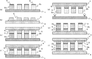
- FIG. 4 is an explanatory diagram illustrating an example of a method for manufacturing the thermoelectric conversion module of the present invention (method for manufacturing a ⁇ -type thermoelectric conversion module), and FIG. 4A is one of the thermoelectric conversion material layers (chips).
- FIG. 4 (b) is a cross-sectional view after forming a solder receiving layer described later on a surface (upper surface)
- FIG. 4 (b) is a cross-sectional view after forming an electrode and a solder material layer on a resin film
- FIG. 4 (c) The electrode on the resin film obtained in FIG.
- thermoelectric conversion material layer (chip) was bonded to one surface (upper surface) of the thermoelectric conversion material layer (chip) with the solder material layer and the solder receiving layer of FIG. 4 (a) interposed therebetween.
- 4 (c') is a cross-sectional view after joining the solder material layers by heating and cooling
- FIG. 4 (d) is a cross-sectional view after joining the solder material layers by heating and cooling
- FIG. 4 (d) is the other surface of the thermoelectric conversion material layer (chip) from the substrate. It is a cross-sectional view after peeling off the lower surface)
- FIG. 4 (e) shows a solder receiving layer on the other surface (lower surface) of the thermoelectric conversion material layer (chip) on the resin film obtained in FIG. 4 (d).
- FIG. 4 (f) is a cross-sectional view of the resin film obtained in FIG. 4 (b) with the solder material layer and the solder receiving layer of FIG. 4 (e) interposed therebetween. It is sectional drawing after bonding and joining with the other surface (lower surface) of a layer (chip).
- the electrode forming step is a step of preparing a first layer having the first resin film and the first electrode in this order in the above (iii) of the method for manufacturing a thermoelectric conversion module, on the first resin film. This is a step of forming the first electrode.
- the step of preparing the second layer having the second resin film and the second electrode in this order in the above (iv) it is a step of forming the second electrode on the second resin film.
- a metal layer is formed on the resin film 4 and processed into a predetermined pattern to form an electrode 5.
- the first resin film and the second resin film may be resin films of the same material or resin films of different materials. It has excellent flexibility, and even when a coating film (thin film) made of a thermoelectric semiconductor composition is fired (annealed), the resin film can maintain the performance of the thermoelectric element without being thermally deformed, and has heat resistance and dimensions.
- a polyimide film, a polyamide film, a polyetherimide film, a polyaramid film, and a polyamideimide film are preferable from the viewpoint of high stability, and a polyimide film is particularly preferable from the viewpoint of high versatility.
- the thicknesses of the first resin film and the second resin film are independently, preferably 1 to 1000 ⁇ m, more preferably 5 to 500 ⁇ m, and particularly preferably 10 independently from the viewpoints of flexibility, heat resistance, and dimensional stability. It is ⁇ 100 ⁇ m.
- the 5% mass reduction temperature of the first resin film and the second resin film measured by thermogravimetric analysis (TG) is preferably 300 ° C. or higher, more preferably 400 ° C. or higher.
- the heating dimensional change rate measured at 200 ° C. according to JIS K7133 (1999) is preferably 0.5% or less, more preferably 0.3% or less.
- the coefficient of linear expansion in the plane direction measured according to JIS K7197 (2012) is preferably 0.1 to 50 ppm ⁇ ° C. -1 , and more preferably 0.1 to 30 ppm ⁇ ° C. -1 .
- the metal materials of the first electrode and the second electrode of the thermoelectric conversion module are independently copper, gold, nickel, aluminum, rhodium, platinum, chromium, palladium, stainless steel, molybdenum, or any of these metals. Examples include alloys containing. One of these may be used alone, or two or more thereof may be used in combination.
- the thickness of the layer of the electrode (metal material) is preferably 10 nm to 200 ⁇ m, more preferably 30 nm to 150 ⁇ m, and particularly preferably 50 nm to 120 ⁇ m. When the thickness of the layer of the electrode (metal material) is within the above range, the electrical conductivity is high and the resistance is low, and sufficient strength as an electrode can be obtained.
- the electrode is formed using the metal material described above.
- a method of forming the electrode a predetermined method is performed by providing an electrode having no pattern formed on the resin film, and then performing a known physical treatment or chemical treatment mainly based on a photolithography method, or using them in combination.
- a method of processing into the pattern shape of the above, a method of directly forming an electrode pattern by a screen printing method, an inkjet method, or the like can be mentioned.
- PVD Physical Vapor Deposition Method
- CVD Chemical Vapor Deposition
- thermal CVD thermal CVD
- atomic layer deposition ALD
- Dry processes such as vapor deposition method
- various coating methods such as dip coating method, spin coating method, spray coating method, gravure coating method, die coating method, doctor blade method, and wet processes such as electrodeposition method; silver salt method; Electrolytic plating method; electroless plating method; lamination of metal foil; and the like, which are appropriately selected depending on the material of the electrode.
- an electrode formed by a plating method or a vacuum film forming method Since high conductivity and high thermal conductivity are required for the electrode from the viewpoint of maintaining thermoelectric performance, it is preferable to use an electrode formed by a plating method or a vacuum film forming method. Since high conductivity and high thermal conductivity can be easily realized, a vacuum film forming method such as a vacuum vapor deposition method or a sputtering method; an electrolytic plating method; an electrolytic plating method; or the like is preferable. Although it depends on the dimensional and dimensional accuracy requirements of the forming pattern, the pattern can be easily formed by interposing a hard mask such as a metal mask.
- the first electrode joining step is the step (v) of the method for manufacturing a thermoelectric conversion module, and one surface of the thermoelectric conversion material layer (chip) obtained in the step (ii) and the above (iii). ) Is a step of joining the first electrode of the first layer prepared in the step of) with the first bonding material layer interposed therebetween.
- the solder material layer 6 on the electrode 5 of the resin film 4 and the thermoelectric conversion material layer (P-type chip) 2a made of a P-type thermoelectric conversion material are used.
- a solder receiving layer 3 formed on one surface of each of the thermoelectric conversion material layer (N-type chip) 2b made of N-type thermoelectric conversion material, and the P-type chip 2a and the N-type chip 2b are attached to the electrode 5.
- the solder material layer 6 is heated to a predetermined temperature, held for a predetermined time, and then returned to room temperature to join the P-type chip 2a and the N-type chip 2b to the electrode 5.
- the heating temperature, holding time, etc. will be described later.
- FIG. 4C' is an embodiment after the solder material layer 6 is returned to room temperature (the solder material layer 6'is solidified by heating and cooling and its thickness is reduced).
- the first electrode joining step includes a first joining material layer forming step.
- the first bonding material layer forming step is a step of forming a first bonding material layer on the first electrode obtained in the above step (iii) in the step (v) of the method for manufacturing a thermoelectric conversion module. be.
- the first bonding material layer forming step is, for example, in FIG. 4B, a step of forming the solder material layer 6 on the electrode 5.
- the bonding material constituting the first bonding material layer include a solder material, a conductive adhesive, a sintered bonding agent, and the like, and in this order, a solder material layer, a conductive adhesive layer, and a sintered bonding agent layer, respectively. It is preferable that the solder is formed on the electrode.
- the conductivity means that the electrical resistivity is less than 1 ⁇ 10 6 ⁇ ⁇ m.
- the solder material constituting the solder material layer may be appropriately selected in consideration of conductivity and thermal conductivity.
- Bi / Pb alloys Sn / Bi / Zn alloys, Sn / Bi alloys, Sn / Bi / Pb alloys, Sn / Pb / Cd alloys, Sn / Cd alloys and the like.
- One of these may be used alone, or two or more thereof may be used in combination.
- the thickness of the solder material layer (after heating and cooling) is preferably 10 to 200 ⁇ m, more preferably 20 to 150 ⁇ m, further preferably 30 to 130 ⁇ m, and particularly preferably 40 to 120 ⁇ m. When the thickness of the solder material layer is within this range, it becomes easy to obtain the adhesion of the thermoelectric conversion material to the chip and the electrode.
- Examples of the method of applying the solder material on the substrate include known methods such as stencil printing, screen printing, and dispensing method.
- the heating conditions vary depending on the solder material used, the resin film, etc., but are usually carried out at 150 to 280 ° C. for 3 to 20 minutes.
- solder material layer When a solder material layer is used, it is preferable to join the solder material layer via a solder receiving layer, which will be described later, from the viewpoint of improving the adhesion of the thermoelectric conversion material to the chip.
- the conductive adhesive constituting the conductive adhesive layer is not particularly limited, and examples thereof include a conductive paste and a binder. One of these may be used alone, or two or more thereof may be used in combination.
- Examples of the conductive paste include copper paste, silver paste, nickel paste and the like. One of these may be used alone, or two or more thereof may be used in combination.
- Examples of the binder include epoxy resin, acrylic resin, urethane resin and the like. One of these may be used alone, or two or more thereof may be used in combination.
- Examples of the method of applying the conductive adhesive on the resin film include known methods such as screen printing and a dispensing method. One of these may be used alone, or two or more thereof may be used in combination.
- the thickness of the conductive adhesive layer is preferably 10 to 200 ⁇ m, more preferably 20 to 150 ⁇ m, still more preferably 30 to 130 ⁇ m, and particularly preferably 40 to 120 ⁇ m.
- the sintered bonding agent constituting the sintered bonding agent layer is not particularly limited, and examples thereof include a sintered paste and the like.
- Sintering paste is composed of, for example, micron-sized metal powder and nano-sized metal particles, and unlike conductive adhesives, it directly bonds metals by sintering, and is used for epoxy resin, acrylic resin, urethane resin, etc. Resin may be contained.
- the sintering paste include silver sintering paste and copper sintering paste. One of these may be used alone, or two or more thereof may be used in combination.
- Examples of the method of applying the sintered bonding agent layer on the resin film include known methods such as screen printing, stencil printing, and dispensing method.
- the sintering conditions vary depending on the metal material used and the like, but are usually 100 to 300 ° C. for 30 to 120 minutes.
- Commercially available sintered bonding agents include, for example, silver sintering paste, sintered paste (manufactured by Kyocera, product name: CT2700R7S), sintered metal bonding material (manufactured by Nihon Handa, product name: MAX102), and the like. Can be used.
- the thickness of the sintered bonding agent layer is preferably 10 to 200 ⁇ m, more preferably 20 to 150 ⁇ m, still more preferably 30 to 130 ⁇ m, and particularly preferably 40 to 120 ⁇ m.
- thermoelectric conversion module for example, when manufacturing a ⁇ -type thermoelectric conversion module or an in-plane type thermoelectric conversion module, the thermoelectric conversion after the firing (annealing) treatment obtained in the above step (ii) is further performed. It is preferable to include a step of forming a solder receiving layer on one surface of the chip of the material.
- the solder receiving layer forming step is a step of forming a solder receiving layer on a thermoelectric conversion material layer (chip) made of a thermoelectric conversion material.
- a thermoelectric conversion material layer chip
- it is made of a P-type thermoelectric conversion material.
- This is a step of forming a solder receiving layer 3 on one surface of a thermoelectric conversion material layer (N-type chip) 2b composed of a thermoelectric conversion material layer (P-type chip) 2a and an N-type thermoelectric conversion material.
- the solder receiving layer preferably contains a metal material.
- the metal material is preferably at least one selected from gold, silver, aluminum, rhodium, platinum, chromium, palladium, tin, and alloys containing any of these metal materials.
- a two-layer structure of gold, silver, aluminum, or tin and gold is preferable, and silver and aluminum are more preferable from the viewpoint of material cost, high thermal conductivity, and bonding stability.
- the solder receiving layer may be formed by using a paste material containing a solvent or a resin component in addition to the metal material. When a paste material is used, it is preferable to remove the solvent and the resin component by firing or the like as described later.
- As the paste material silver paste and aluminum paste are preferable.
- the thickness of the solder receiving layer is preferably 10 nm to 50 ⁇ m, more preferably 50 nm to 16 ⁇ m, further preferably 200 nm to 4 ⁇ m, and particularly preferably 500 nm to 3 ⁇ m.
- the adhesion to the surface of the thermoelectric conversion material layer (chip) made of the thermoelectric conversion material and the adhesion to the surface of the solder material layer on the electrode side are excellent, and reliability is excellent. Highly bonded. Further, since the thermal conductivity can be maintained high as well as the conductivity, the thermoelectric performance of the thermoelectric conversion module is not deteriorated as a result and is maintained.
- a metal material may be formed as it is and used as a single layer, or two or more metal materials may be laminated and used as a multi-layer. Further, a film may be formed as a composition in which a metal material is contained in a solvent, a resin or the like. However, in this case, from the viewpoint of maintaining high conductivity and high thermal conductivity (maintaining thermoelectric performance), as the final form of the solder receiving layer, the resin component including the solvent may be removed by firing or the like. preferable.
- the solder receiving layer is preferably formed using the above-mentioned metal material.
- a method of forming the solder receiving layer after providing a solder receiving layer in which a pattern is not formed on the thermoelectric conversion material layer (chip), a known physical treatment or chemical treatment mainly based on a photolithography method is performed. Alternatively, a method of processing into a predetermined pattern shape by using them in combination, or a method of directly forming a pattern of the solder receiving layer by a screen printing method, a stencil printing method, an inkjet method, or the like can be mentioned.
- PVD Physical Vapor Deposition Method
- Vacuum film deposition methods such as chemical vapor deposition
- various coatings such as dip coating method, spin coating method, spray coating method, gravure coating method, die coating method, doctor blade method; wet process such as electrodeposition method; silver Examples thereof include a salt method; an electrolytic plating method; a non-electrolytic plating method; a lamination of metal foils; and the like, which are appropriately selected depending on the material of the solder receiving layer.
- solder receiving layer is required to have high conductivity and high thermal conductivity from the viewpoint of maintaining thermoelectric performance
- a screen printing method, a stencil printing method, an electrolytic plating method, an electrolytic plating method, or a vacuum film forming method can be used. It is preferable to use the formed solder receiving layer.
- the chip batch peeling step is the step (vi) of the method for manufacturing a thermoelectric conversion module, and is a step of peeling the other surface of the thermoelectric conversion material layer (chip) after the step (v) from the substrate.
- the chip batch peeling step for example, in FIG. 4D, the thermoelectric conversion material layer (P-type chip) 2a made of the P-type thermoelectric conversion material from the substrate 1 and the thermoelectric conversion material layer made of the N-type thermoelectric conversion material ( This is a step of collectively peeling off the other surface of the N-type chip) 2b.
- the method for peeling the thermoelectric conversion material layer is not particularly limited as long as it can peel off all the thermoelectric conversion material layers (chips) from the substrate at once.
- the second electrode joining step is included in the step (vii) of the method for manufacturing a thermoelectric conversion module, and is the other of the thermoelectric conversion material layer (chip) obtained by peeling in the step (vi). This is a step of joining the surface and the second electrode of the second layer of the second A prepared in the step (iv) via the second joining material layer.
- a thermoelectric conversion material layer (P-type chip) 2a made of a P-type thermoelectric conversion material and a thermoelectric conversion material layer (N-type) made of an N-type thermoelectric conversion material.
- the material of the second electrode and the second resin film of the second layer the same materials as those described in the first electrode joining step can be used, and the joining method is also the same. It is preferable that the electrode is bonded via the solder material layer, the conductive adhesive layer, or the sintered bonding agent layer described above.
- the second electrode bonding step includes a second bonding material layer forming step.
- the second bonding material layer forming step in the step (vii) of the method for manufacturing a thermoelectric conversion module, the second bonding material layer is formed on the second electrode of the layer 2A prepared in the step (iv). This is the process of forming.
- the second bonding material layer the same material as the first bonding material layer described above can be used, and the forming method, thickness, and the like are all the same.
- thermoelectric conversion material layer when a solder material layer is used in manufacturing a ⁇ -type thermoelectric conversion module, it is further formed on the other surface of the thermoelectric conversion material layer (chip) obtained by peeling in the step (vi). It is preferable to include a step of forming a solder receiving layer.
- a solder receiving layer For example, in FIG. 4E, the other surface of the thermoelectric conversion material layer (P-type chip) 2a made of P-type thermoelectric conversion material and the thermoelectric conversion material layer (N-type chip) 2b made of N-type thermoelectric conversion material. This is a step of forming the solder receiving layer 3.
- thermoelectric conversion module except when the electrodes are not provided on any of the pair of resin films
- thermoelectric conversion is performed. From the viewpoint of preventing mechanical deformation of the module and suppressing deterioration of thermoelectric performance, it is preferable to use a combination of solder material layers, conductive adhesive layers, or sintered bonding agent layers.
- the resin film joining step is included in the step (vii) of the method for manufacturing a thermoelectric conversion module, and is combined with the other surface of the thermoelectric conversion material layer (chip) obtained by peeling off in the step (vi).
- This is a step of joining the second B layer having the second resin film and having no electrode prepared in the above step (iv) via the third bonding material layer.
- the second resin film is as described above.
- a third bonding material layer is used for bonding with the second layer B having the second resin film and having no electrodes.
- the bonding material constituting the third bonding material layer is preferably a resin material, and is formed on the resin film as the resin material layer.
- the resin material preferably contains a polyolefin-based resin, an epoxy-based resin, or an acrylic-based resin. Further, the resin material preferably has adhesiveness and low water vapor permeability. In the present specification, having adhesiveness means that the resin material has adhesiveness, adhesiveness, and pressure-sensitive adhesiveness that can be adhered by pressure at the initial stage of sticking.
- the resin material layer can be formed by a known method.
- the thickness of the resin material layer is preferably 1 to 100 ⁇ m, more preferably 3 to 50 ⁇ m, and particularly preferably 5 to 30 ⁇ m.
- thermoelectric conversion module Another example of the method for manufacturing the thermoelectric conversion module is as follows. Specifically, a plurality of chips are peeled off from the substrate described above for each chip to obtain a plurality of chips, and the plurality of chips are arranged one by one on a predetermined electrode on a resin film. This is a method of forming a thermoelectric conversion module by going through the steps. As a method of arranging a plurality of chips on the electrodes, a known method such as handling each chip with a robot or the like, aligning with a microscope or the like, and arranging the chips can be used.
- thermoelectric conversion module chips can be formed by a simple method, and in a thermoelectric conversion module in which a plurality of chips are combined, a thermoelectric semiconductor composition in a conventional firing (annealing) treatment step is used. It is possible to prevent a decrease in thermoelectric performance due to the formation of an alloy layer due to diffusion between the electrode and the electrode.
- test piece (chip) made of the thermoelectric conversion material produced in Examples and Comparative Examples (a) measurement of the filling rate of the vertical cross section along the thickness direction, and (b) evaluation of electrical characteristics (measurement of electrical resistance value) are performed.
- the method was as follows.
- thermoelectric conversion material layer 6 of the thermoelectric conversion material layer.
- the rate was calculated.
- an SEM image (longitudinal section) having a magnification of 500 times is used, and the measurement range is set to a range surrounded by 1280 pixels in the width direction and 220 pixels in the thickness direction with respect to an arbitrary position of the thermoelectric conversion material layer.
- Cut out as an image The cut-out image is binarized from "Brightness / Control" with the maximum contrast, and the dark part and the bright part in the binarization process are regarded as the thermoelectric conversion material, and the thermoelectric conversion material is used in "Threshold".
- the filling rate of was calculated.
- the filling rate was calculated for three SEM images and used as the average value thereof.
- thermoelectric semiconductor composition Preparation of thermoelectric semiconductor particles
- P-type bismuth tellurium Bi 0.4 Te 3.0 Sb 1.6 manufactured by High Purity Chemical Laboratory, particle size: 20 ⁇ m
- Thermoelectric semiconductor particles having an average particle size of 2.5 ⁇ m were prepared by pulverizing in a nitrogen gas atmosphere using line P-7).
- thermoelectric semiconductor particles obtained by pulverization were measured by a laser diffraction type particle size analyzer (Mastersizer 3000 manufactured by Malvern).
- Mastersizer 3000 manufactured by Malvern Preparation of thermoelectric semiconductor composition
- P-type bismasterlide Bi 0.4 Te 3.0 Sb 1.6 particles (average particle size 2.5 ⁇ m) obtained above 77.0 parts by mass, polyethylene carbonate as a binder resin (final decomposition temperature: 250 ° C.)
- Polyethylene carbonate solution manufactured by EMPOWER MATERIALS, QPAC25, solvent: N-methylpyrrolidone, solid content concentration: 20% by mass) 16.5 parts by mass (solid content 3.3 parts by mass), and 1- as an ionic liquid.
- thermoelectric semiconductor composition in which 6.5 parts by mass of butylpyridinium bromide (manufactured by Koei Chemical Industry Co., Ltd., IL-P18B) was mixed and dispersed was prepared.
- test piece chip made of thermoelectric conversion material (formation of thermoelectric conversion material layer)
- a metal mask material: magnetic SUS, thickness: 50 ⁇ m
- a capton film manufactured by Ube Kosan Co., Ltd.
- thermoelectric semiconductor composition other than the thermoelectric semiconductor composition filled in the opening is removed with a metal squeegee, and the thermoelectric semiconductor composition is applied by heating and drying at 120 ° C. for 10 minutes.
- a film (thin film) was prepared.
- the metal mask had an opening of 1.95 mm ⁇ 1.95 mm and a thickness of 450 to 550 ⁇ m according to the shape of the coating film to be produced. After heat-drying, the coating film (thin film) was removed from the metal mask, and further, the coating film (thin film) was peeled off from the Kapton film, and heat and pressure treatment was performed.
- This heating and pressurizing treatment is performed using a hydraulic press machine (tabletop test press SA-302 manufactured by Tester Sangyo Co., Ltd.) at 250 ° C. in an atmospheric atmosphere at 110 MPa with respect to the entire upper surface of the coating film (thin film).
- the pressurization treatment was performed for 10 minutes.
- a frame having an opening corresponding to the target shape is arranged so as to surround the periphery of the coating film, and then the coating film ( The thin film) was pressurized.
- thermoelectric conversion material layer was formed.
- Example 2 In Example 1, "a polyethylene carbonate solution containing polyethylene carbonate as a binder resin (final decomposition temperature: 250 ° C.) (manufactured by EMPOWER MATERIALS, QPAC25, solvent: N-methylpyrrolidone, solid content concentration: 20% by mass) 16.
- Example 3 In Example 1, "a polyethylene carbonate solution containing polyethylene carbonate as a binder resin (final decomposition temperature: 250 ° C.) (manufactured by EMPOWER MATERIALS, QPAC25, solvent: N-methylpyrrolidone, solid content concentration: 20% by mass) 16.
- Example 4 In Example 1, "a polyethylene carbonate solution containing polyethylene carbonate as a binder resin (final decomposition temperature: 250 ° C.) (manufactured by EMPOWER MATERIALS, QPAC25, solvent: N-methylpyrrolidone, solid content concentration: 20% by mass) 16.
- thermoelectric semiconductor composition instead of using “5 parts by mass (solid content 3.3 parts by mass)", a poly (propylene / cyclohexene) carbonate solution (EMPOWER) containing “poly (propylene / cyclohexene) carbonate as a binder resin (final decomposition temperature: 350 ° C.)" Same as in Example 1 except that 16.5 parts by mass (solid content 3.3 parts by mass) ”manufactured by MATERIALS, QPAC100, solvent: N-methylpyrrolidone, solid content concentration: 20% by mass was used. , "(1) Preparation of thermoelectric semiconductor composition” and “(2) Preparation of test piece (chip) made of thermoelectric conversion material” were carried out.
- Example 5 In Example 1, "P-type bismasterlide Bi 0.4 Te 3.0 Sb 1.6 particles (average particle size 2.5 ⁇ m) 77.0 parts by mass, polyethylene carbonate as a binder resin (final decomposition temperature: 250 ° C.) ) In a polyethylene carbonate solution (manufactured by EMPOWER MATERIALS, QPAC25, solvent: N-methylpyrrolidone, solid content concentration: 20% by mass) 16.5 parts by mass (solid content 3.3 parts by mass), and 1- as an ionic liquid.
- thermoelectric semiconductor composition in which 6.5 parts by mass of butylpyridinium bromide (IL-P18B, manufactured by Koei Chemical Industry Co., Ltd.) is mixed and dispersed
- IL-P18B butylpyridinium bromide
- Ethyl cellulose solution containing 6 particles (average particle size 2.5 ⁇ m) 79.0 parts by mass and ethyl cellulose as a binder resin (final decomposition temperature: 450 ° C.) Etocell 4CPS, manufactured by Nissin Kasei Co., Ltd., solvent: N-methylpyrrolidone) , Solid content concentration: 5% by mass) 17.0 parts by mass (solid content 0.85 parts by mass), and 1-butylpyridinium bromide (manufactured by Koei Chemical Industry Co., Ltd., IL-P18B) 3.95 parts by mass as an ionic liquid "(1) Preparation of thermoelectric semiconductor composition” and "(2) Test piece (chip) made of thermoelectric conversion material” in the same manner as in Example 1 except that "thermoelectric semiconductor composition mixed and dispersed” was used.
- Etocell 4CPS manufactured by Nissin Kasei Co., Ltd., solvent: N-methylpyrrolidone
- Example 1 a polyethylene carbonate solution containing polyethylene carbonate as a binder resin (final decomposition temperature: 250 ° C.) (manufactured by EMPOWER MATERIALS, QPAC25, solvent: N-methylpyrrolidone, solid content concentration: 20% by mass) 16.
- Example 2 In Example 1, "a polyethylene carbonate solution containing polyethylene carbonate as a binder resin (final decomposition temperature: 250 ° C.) (manufactured by EMPOWER MATERIALS, QPAC25, solvent: N-methylpyrrolidone, solid content concentration: 20% by mass) 16.
- test pieces (chips) made of the thermoelectric conversion materials of Examples 1 to 5 in which the filling rate of the thermoelectric conversion material in the vertical cross section along the thickness direction of the thermoelectric conversion material layer is more than 0.900 and less than 1.000 have a filling rate. It can be seen that the electrical resistivity can be reduced as compared with the test piece (chip) made of the thermoelectric conversion materials of Comparative Examples 1 and 2 having a value of 0.900 or less.
- thermoelectric conversion module of the present invention is applied to power generation applications that convert exhaust heat from various combustion furnaces such as factories, waste combustion furnaces, cement combustion furnaces, automobile combustion gas exhaust heat, and electronic equipment exhaust heat into electricity. Can be considered.
- various combustion furnaces such as factories, waste combustion furnaces, cement combustion furnaces, automobile combustion gas exhaust heat, and electronic equipment exhaust heat into electricity.
- electronic equipment exhaust heat into electricity.
- for cooling applications for example, CPUs (Central Processing Units) used in smartphones, various computers, etc., CMOS (Complementary Microelectromechanical Systems Sensors), CCD (Challge Coupled Devices), and other image sensors, , MEMS (Micro Electro Mechanical Systems), temperature control of various sensors such as light receiving elements, etc. can be considered.
- CPUs Central Processing Units
- CCD Challge Coupled Devices
- MEMS Micro Electro Mechanical Systems
- Substrate 2a Thermoelectric conversion material layer (P-type chip) made of P-type thermoelectric conversion material 2b: Thermoelectric conversion material layer (N-type chip) made of N-type thermoelectric conversion material 3: Solder receiving layer 4: Resin film 5: Electrode 6: Solder material layer (at the time of formation) 6': Solder material layer (after joining) 12: Coating film 12a of thermoelectric semiconductor composition: Coating film 12b: Coating film 20, 20s, 20t: Thermoelectric conversion material layer 30: Void portion 30b: Void portion 40b: Void portion X: Length (width direction) Y: Length (depth direction) D: Thickness (thickness direction) Dmax: Maximum value of thickness in the thickness direction (longitudinal section) Dmin: Minimum value of thickness in the thickness direction (longitudinal section) C: Central part of thermoelectric conversion material layer
Landscapes
- Chemical & Material Sciences (AREA)
- Inorganic Chemistry (AREA)
- Engineering & Computer Science (AREA)
- Manufacturing & Machinery (AREA)
- Compositions Of Macromolecular Compounds (AREA)
Priority Applications (3)
| Application Number | Priority Date | Filing Date | Title |
|---|---|---|---|
| JP2022510042A JPWO2021193357A1 (https=) | 2020-03-25 | 2021-03-18 | |
| CN202180024577.4A CN115336017A (zh) | 2020-03-25 | 2021-03-18 | 热电转换模块 |
| US17/913,487 US12239020B2 (en) | 2020-03-25 | 2021-03-18 | Thermoelectric conversion module |
Applications Claiming Priority (2)
| Application Number | Priority Date | Filing Date | Title |
|---|---|---|---|
| JP2020-054840 | 2020-03-25 | ||
| JP2020054840 | 2020-03-25 |
Publications (1)
| Publication Number | Publication Date |
|---|---|
| WO2021193357A1 true WO2021193357A1 (ja) | 2021-09-30 |
Family
ID=77891711
Family Applications (1)
| Application Number | Title | Priority Date | Filing Date |
|---|---|---|---|
| PCT/JP2021/011109 Ceased WO2021193357A1 (ja) | 2020-03-25 | 2021-03-18 | 熱電変換モジュール |
Country Status (5)
| Country | Link |
|---|---|
| US (1) | US12239020B2 (https=) |
| JP (1) | JPWO2021193357A1 (https=) |
| CN (1) | CN115336017A (https=) |
| TW (1) | TWI890761B (https=) |
| WO (1) | WO2021193357A1 (https=) |
Citations (6)
| Publication number | Priority date | Publication date | Assignee | Title |
|---|---|---|---|---|
| JPS6442184A (en) * | 1987-08-08 | 1989-02-14 | Daiwa Shinku Corp | Manufacture of thermocouple |
| JP2013219095A (ja) * | 2012-04-05 | 2013-10-24 | Toyota Industries Corp | 熱電材料及びその製造方法 |
| WO2016104615A1 (ja) * | 2014-12-26 | 2016-06-30 | リンテック株式会社 | ペルチェ冷却素子及びその製造方法 |
| JP2017098284A (ja) * | 2015-11-18 | 2017-06-01 | 日東電工株式会社 | 半導体装置の製造方法 |
| JP2017098282A (ja) * | 2015-11-18 | 2017-06-01 | 日東電工株式会社 | 半導体装置の製造方法 |
| WO2018168837A1 (ja) * | 2017-03-16 | 2018-09-20 | リンテック株式会社 | 熱電変換モジュール用電極材料及びそれを用いた熱電変換モジュール |
Family Cites Families (10)
| Publication number | Priority date | Publication date | Assignee | Title |
|---|---|---|---|---|
| JP2002033525A (ja) * | 2000-07-13 | 2002-01-31 | Nhk Spring Co Ltd | 熱電素子とその製造方法 |
| WO2008140596A2 (en) * | 2006-12-01 | 2008-11-20 | Massachusetts Institute Of Technology (Mit) | Methods for high figure-of-merit in nanostructured thermoelectric materials |
| CN101656292B (zh) | 2009-09-16 | 2011-04-20 | 北京科技大学 | 一种铋碲系纳米多孔热电材料的制备方法 |
| CN104465977B (zh) * | 2011-07-20 | 2018-05-01 | 中弥浩明 | 热电转变元件和热电转变发电装置 |
| EP3475990B1 (en) * | 2016-06-23 | 2020-08-05 | 3M Innovative Properties Company | Thermoelectric tape |
| WO2018143598A1 (ko) | 2017-02-01 | 2018-08-09 | 엘지이노텍 주식회사 | 열전 소결체 및 열전소자 |
| WO2019009202A1 (ja) | 2017-07-05 | 2019-01-10 | 三菱マテリアル株式会社 | 熱電変換モジュール、及び、熱電変換モジュールの製造方法 |
| CN108963064B (zh) | 2017-12-28 | 2019-11-29 | 中国科学院物理研究所 | 热压烧结装置、微纳多孔结构的块体热电材料及其制法 |
| US20210098672A1 (en) | 2018-03-26 | 2021-04-01 | Lintec Corporation | Thermoelectric conversion module |
| US10892396B2 (en) * | 2018-06-19 | 2021-01-12 | The Regents Of The University Of Michigan | Stabilized copper selenide thermoelectric materials and methods of fabrication thereof |
-
2021
- 2021-03-18 WO PCT/JP2021/011109 patent/WO2021193357A1/ja not_active Ceased
- 2021-03-18 US US17/913,487 patent/US12239020B2/en active Active
- 2021-03-18 CN CN202180024577.4A patent/CN115336017A/zh active Pending
- 2021-03-18 JP JP2022510042A patent/JPWO2021193357A1/ja active Pending
- 2021-03-23 TW TW110110348A patent/TWI890761B/zh active
Patent Citations (6)
| Publication number | Priority date | Publication date | Assignee | Title |
|---|---|---|---|---|
| JPS6442184A (en) * | 1987-08-08 | 1989-02-14 | Daiwa Shinku Corp | Manufacture of thermocouple |
| JP2013219095A (ja) * | 2012-04-05 | 2013-10-24 | Toyota Industries Corp | 熱電材料及びその製造方法 |
| WO2016104615A1 (ja) * | 2014-12-26 | 2016-06-30 | リンテック株式会社 | ペルチェ冷却素子及びその製造方法 |
| JP2017098284A (ja) * | 2015-11-18 | 2017-06-01 | 日東電工株式会社 | 半導体装置の製造方法 |
| JP2017098282A (ja) * | 2015-11-18 | 2017-06-01 | 日東電工株式会社 | 半導体装置の製造方法 |
| WO2018168837A1 (ja) * | 2017-03-16 | 2018-09-20 | リンテック株式会社 | 熱電変換モジュール用電極材料及びそれを用いた熱電変換モジュール |
Also Published As
| Publication number | Publication date |
|---|---|
| CN115336017A (zh) | 2022-11-11 |
| TW202141816A (zh) | 2021-11-01 |
| JPWO2021193357A1 (https=) | 2021-09-30 |
| TWI890761B (zh) | 2025-07-21 |
| US20230133754A1 (en) | 2023-05-04 |
| US12239020B2 (en) | 2025-02-25 |
Similar Documents
| Publication | Publication Date | Title |
|---|---|---|
| JP7346427B2 (ja) | 熱電変換材料のチップの製造方法及びその製造方法により得られたチップを用いた熱電変換モジュールの製造方法 | |
| US20210098672A1 (en) | Thermoelectric conversion module | |
| JPWO2018168837A1 (ja) | 熱電変換モジュール用電極材料及びそれを用いた熱電変換モジュール | |
| JP7348192B2 (ja) | 半導体素子 | |
| JP7543140B2 (ja) | 熱電変換材料のチップ | |
| JP7458375B2 (ja) | 熱電変換材料のチップの製造方法 | |
| JP6937452B1 (ja) | 熱電変換体、熱電変換モジュール、及び、熱電変換体の製造方法 | |
| JP7401361B2 (ja) | 熱電変換モジュール | |
| JP7770192B2 (ja) | 熱電変換モジュール及びその製造方法 | |
| WO2021193357A1 (ja) | 熱電変換モジュール | |
| JP7760277B2 (ja) | 熱電変換材料層 | |
| WO2022071043A1 (ja) | 熱電変換材料層 | |
| JP2022057937A (ja) | 熱電変換モジュール用電極 | |
| JP7698969B2 (ja) | 熱電変換モジュール | |
| JP2024143431A (ja) | ペルチェ冷却熱電変換モジュール | |
| WO2020203611A1 (ja) | 熱電変換材料のチップへのハンダ受理層形成方法 | |
| JP2021192409A (ja) | 熱電変換モジュール用電極 |
Legal Events
| Date | Code | Title | Description |
|---|---|---|---|
| 121 | Ep: the epo has been informed by wipo that ep was designated in this application |
Ref document number: 21774004 Country of ref document: EP Kind code of ref document: A1 |
|
| ENP | Entry into the national phase |
Ref document number: 2022510042 Country of ref document: JP Kind code of ref document: A |
|
| NENP | Non-entry into the national phase |
Ref country code: DE |
|
| 122 | Ep: pct application non-entry in european phase |
Ref document number: 21774004 Country of ref document: EP Kind code of ref document: A1 |
|
| WWG | Wipo information: grant in national office |
Ref document number: 17913487 Country of ref document: US |