WO2021192928A1 - カードエッジコネクタ及び回路基板 - Google Patents
カードエッジコネクタ及び回路基板 Download PDFInfo
- Publication number
- WO2021192928A1 WO2021192928A1 PCT/JP2021/008735 JP2021008735W WO2021192928A1 WO 2021192928 A1 WO2021192928 A1 WO 2021192928A1 JP 2021008735 W JP2021008735 W JP 2021008735W WO 2021192928 A1 WO2021192928 A1 WO 2021192928A1
- Authority
- WO
- WIPO (PCT)
- Prior art keywords
- housing
- terminal
- circuit board
- mounting surface
- board
- Prior art date
Links
Images


Classifications
-
- H—ELECTRICITY
- H01—ELECTRIC ELEMENTS
- H01R—ELECTRICALLY-CONDUCTIVE CONNECTIONS; STRUCTURAL ASSOCIATIONS OF A PLURALITY OF MUTUALLY-INSULATED ELECTRICAL CONNECTING ELEMENTS; COUPLING DEVICES; CURRENT COLLECTORS
- H01R12/00—Structural associations of a plurality of mutually-insulated electrical connecting elements, specially adapted for printed circuits, e.g. printed circuit boards [PCB], flat or ribbon cables, or like generally planar structures, e.g. terminal strips, terminal blocks; Coupling devices specially adapted for printed circuits, flat or ribbon cables, or like generally planar structures; Terminals specially adapted for contact with, or insertion into, printed circuits, flat or ribbon cables, or like generally planar structures
- H01R12/70—Coupling devices
- H01R12/71—Coupling devices for rigid printing circuits or like structures
- H01R12/72—Coupling devices for rigid printing circuits or like structures coupling with the edge of the rigid printed circuits or like structures
- H01R12/721—Coupling devices for rigid printing circuits or like structures coupling with the edge of the rigid printed circuits or like structures cooperating directly with the edge of the rigid printed circuits
-
- H—ELECTRICITY
- H01—ELECTRIC ELEMENTS
- H01R—ELECTRICALLY-CONDUCTIVE CONNECTIONS; STRUCTURAL ASSOCIATIONS OF A PLURALITY OF MUTUALLY-INSULATED ELECTRICAL CONNECTING ELEMENTS; COUPLING DEVICES; CURRENT COLLECTORS
- H01R12/00—Structural associations of a plurality of mutually-insulated electrical connecting elements, specially adapted for printed circuits, e.g. printed circuit boards [PCB], flat or ribbon cables, or like generally planar structures, e.g. terminal strips, terminal blocks; Coupling devices specially adapted for printed circuits, flat or ribbon cables, or like generally planar structures; Terminals specially adapted for contact with, or insertion into, printed circuits, flat or ribbon cables, or like generally planar structures
- H01R12/70—Coupling devices
- H01R12/71—Coupling devices for rigid printing circuits or like structures
- H01R12/712—Coupling devices for rigid printing circuits or like structures co-operating with the surface of the printed circuit or with a coupling device exclusively provided on the surface of the printed circuit
- H01R12/716—Coupling device provided on the PCB
-
- H—ELECTRICITY
- H01—ELECTRIC ELEMENTS
- H01R—ELECTRICALLY-CONDUCTIVE CONNECTIONS; STRUCTURAL ASSOCIATIONS OF A PLURALITY OF MUTUALLY-INSULATED ELECTRICAL CONNECTING ELEMENTS; COUPLING DEVICES; CURRENT COLLECTORS
- H01R12/00—Structural associations of a plurality of mutually-insulated electrical connecting elements, specially adapted for printed circuits, e.g. printed circuit boards [PCB], flat or ribbon cables, or like generally planar structures, e.g. terminal strips, terminal blocks; Coupling devices specially adapted for printed circuits, flat or ribbon cables, or like generally planar structures; Terminals specially adapted for contact with, or insertion into, printed circuits, flat or ribbon cables, or like generally planar structures
- H01R12/50—Fixed connections
- H01R12/51—Fixed connections for rigid printed circuits or like structures
- H01R12/55—Fixed connections for rigid printed circuits or like structures characterised by the terminals
- H01R12/57—Fixed connections for rigid printed circuits or like structures characterised by the terminals surface mounting terminals
-
- H—ELECTRICITY
- H01—ELECTRIC ELEMENTS
- H01R—ELECTRICALLY-CONDUCTIVE CONNECTIONS; STRUCTURAL ASSOCIATIONS OF A PLURALITY OF MUTUALLY-INSULATED ELECTRICAL CONNECTING ELEMENTS; COUPLING DEVICES; CURRENT COLLECTORS
- H01R12/00—Structural associations of a plurality of mutually-insulated electrical connecting elements, specially adapted for printed circuits, e.g. printed circuit boards [PCB], flat or ribbon cables, or like generally planar structures, e.g. terminal strips, terminal blocks; Coupling devices specially adapted for printed circuits, flat or ribbon cables, or like generally planar structures; Terminals specially adapted for contact with, or insertion into, printed circuits, flat or ribbon cables, or like generally planar structures
- H01R12/70—Coupling devices
- H01R12/71—Coupling devices for rigid printing circuits or like structures
- H01R12/75—Coupling devices for rigid printing circuits or like structures connecting to cables except for flat or ribbon cables
-
- H—ELECTRICITY
- H01—ELECTRIC ELEMENTS
- H01R—ELECTRICALLY-CONDUCTIVE CONNECTIONS; STRUCTURAL ASSOCIATIONS OF A PLURALITY OF MUTUALLY-INSULATED ELECTRICAL CONNECTING ELEMENTS; COUPLING DEVICES; CURRENT COLLECTORS
- H01R13/00—Details of coupling devices of the kinds covered by groups H01R12/70 or H01R24/00 - H01R33/00
- H01R13/02—Contact members
- H01R13/22—Contacts for co-operating by abutting
- H01R13/24—Contacts for co-operating by abutting resilient; resiliently-mounted
- H01R13/2407—Contacts for co-operating by abutting resilient; resiliently-mounted characterized by the resilient means
-
- H—ELECTRICITY
- H01—ELECTRIC ELEMENTS
- H01R—ELECTRICALLY-CONDUCTIVE CONNECTIONS; STRUCTURAL ASSOCIATIONS OF A PLURALITY OF MUTUALLY-INSULATED ELECTRICAL CONNECTING ELEMENTS; COUPLING DEVICES; CURRENT COLLECTORS
- H01R13/00—Details of coupling devices of the kinds covered by groups H01R12/70 or H01R24/00 - H01R33/00
- H01R13/40—Securing contact members in or to a base or case; Insulating of contact members
-
- H—ELECTRICITY
- H01—ELECTRIC ELEMENTS
- H01R—ELECTRICALLY-CONDUCTIVE CONNECTIONS; STRUCTURAL ASSOCIATIONS OF A PLURALITY OF MUTUALLY-INSULATED ELECTRICAL CONNECTING ELEMENTS; COUPLING DEVICES; CURRENT COLLECTORS
- H01R13/00—Details of coupling devices of the kinds covered by groups H01R12/70 or H01R24/00 - H01R33/00
- H01R13/62—Means for facilitating engagement or disengagement of coupling parts or for holding them in engagement
- H01R13/629—Additional means for facilitating engagement or disengagement of coupling parts, e.g. aligning or guiding means, levers, gas pressure electrical locking indicators, manufacturing tolerances
- H01R13/62983—Linear camming means or pivoting lever for connectors for flexible or rigid printed circuit boards, flat or ribbon cables
-
- H—ELECTRICITY
- H01—ELECTRIC ELEMENTS
- H01R—ELECTRICALLY-CONDUCTIVE CONNECTIONS; STRUCTURAL ASSOCIATIONS OF A PLURALITY OF MUTUALLY-INSULATED ELECTRICAL CONNECTING ELEMENTS; COUPLING DEVICES; CURRENT COLLECTORS
- H01R13/00—Details of coupling devices of the kinds covered by groups H01R12/70 or H01R24/00 - H01R33/00
- H01R13/62—Means for facilitating engagement or disengagement of coupling parts or for holding them in engagement
- H01R13/639—Additional means for holding or locking coupling parts together, after engagement, e.g. separate keylock, retainer strap
Definitions
- This disclosure relates to a card edge connector and a circuit board.
- Patent Document 1 discloses an electric connector in which a circuit board is inserted into a connector housing to which a connector terminal is attached, and elastic contact pieces of terminal fittings are brought into contact with both the front and back surfaces of the circuit board.
- the connector housing receives a reaction force acting on the connector terminal from the circuit board when the elastic contact piece elastically contacts the circuit board. Since the connector housing is made of synthetic resin, the amount of heat shrinkage and the amount of heat expansion are relatively large. Therefore, the contact pressure of the elastic contact piece with respect to the circuit board is not stable. Further, the elastic contact piece of the terminal fitting abuts on the front surface and the back surface of the circuit board in the thickness direction of the circuit board. Therefore, if the thickness dimension of the circuit board varies, the contact pressure of the elastic contact piece with respect to the circuit board is not stable.
- the card edge connector of the first disclosure is completed based on the above circumstances, and an object is to stabilize the contact pressure.
- the circuit board of the second disclosure is completed based on the above circumstances, and an object thereof is to reduce the manufacturing cost.
- the card edge connector of the first disclosure includes a housing, a terminal fitting attached to the housing, and a circuit board having a mounting surface and being fitted to the housing in parallel with the mounting surface.
- the circuit board is provided with a substrate-side terminal in a form protruding from the mounting surface, the terminal fitting is formed with a recess for accommodating the substrate-side terminal, and an elastic contact piece provided in the recess is formed. It makes elastic contact with the substrate-side terminal.
- the circuit board of the second disclosure has a mounting surface and a plurality of board-side terminals in a form protruding from the mounting surface, and when fitted to the housing in parallel with the mounting surface, the circuit board is fitted to the housing.
- the attached terminal fitting comes into contact with the board-side terminal
- the mounting surface has a plurality of support portions, and a mounting member composed of a single component is mounted on the plurality of support portions.
- the plurality of board-side terminals are individually assembled.
- the manufacturing cost can be reduced.
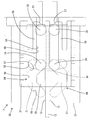
- FIG. 1 is an exploded perspective view of a male connector constituting the card edge connector of the first embodiment.
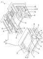
- FIG. 2 is an exploded perspective view of the female side connector constituting the card edge connector.
- FIG. 3 is an exploded perspective view of the terminal module mounted on the circuit board.
- FIG. 4 is a cross-sectional view of the circuit board.
- FIG. 5 is a cross-sectional view taken along line XX of FIG.
- FIG. 6 is a side view showing a state in which the terminal fitting is attached to the housing of the female connector.
- FIG. 7 is a side sectional view showing a state in which the terminal fitting is attached to the housing of the female connector.
- FIG. 8 is a side view showing a state in which the first housing and the terminal fitting are displaced to non-contact positions.
- FIG. 1 is an exploded perspective view of a male connector constituting the card edge connector of the first embodiment.
- FIG. 2 is an exploded perspective view of the female side connector constituting the card edge connector.
- FIG. 9 is a side sectional view showing a state in which the first housing and the terminal fitting are displaced to non-contact positions.
- FIG. 10 is a side view showing a state in which the terminal fitting is displaced to the contact position and connected to the substrate side terminal.
- FIG. 11 is a side sectional view showing a state in which the terminal fitting is displaced to the contact position and connected to the substrate side terminal.
- FIG. 12 is a perspective view showing a state in which the second housing and the third housing are assembled in the second embodiment.
- FIG. 13 is a perspective view showing a state in which the second housing and the third housing are separated.
- FIG. 14 is a perspective view of the circuit board.
- FIG. 15 is a plan sectional view showing a state in which the elastic locking piece of the second housing is locked to the circuit board.
- FIG. 16 is a plan sectional view showing a state in which the second elastic locking piece of the second housing and the third elastic locking piece of the third housing are locked to the circuit board.
- the card edge connector of the first disclosure is (1) A housing, a terminal fitting attached to the housing, and a circuit board having a mounting surface and being fitted to the housing in parallel with the mounting surface are provided. A substrate-side terminal in a form protruding from the mounting surface is provided, and a recess for accommodating the substrate-side terminal is formed in the terminal fitting, and an elastic contact piece provided in the recess serves with respect to the substrate-side terminal. Contact elastically. According to the configuration of the present disclosure, when the elastic contact piece elastically contacts the substrate side terminal, the terminal fitting receives the reaction force from the substrate side terminal. Even if the housing is thermally deformed or the thickness of the circuit board varies, the contact pressure between the terminal fittings and the terminals on the board side is stable.
- the terminal fitting is supported so as to be able to swing between a connection position close to the mounting surface and a non-connection position separated from the mounting surface with the shaft portion as a fulcrum, and the terminal fitting is supported.
- the elastic contact piece is in the connection position, the elastic contact piece is in contact with the substrate side terminal, and when the terminal fitting is in the non-connection position, the elastic contact piece is not in contact with the substrate side terminal.
- the terminal fitting is displaced in the direction of approaching or separating from the mounting surface. There is a need. If an attempt is made to translate the terminal fitting in a direction orthogonal to the mounting surface, the structure for guiding the terminal fitting becomes complicated. In the present disclosure, since the terminal fitting is made to swing, the structure for guiding the terminal fitting can be simplified.
- the housing has a first housing for holding the terminal fitting and a stopper with which the insertion end of the circuit board abuts, and the first housing is connected with the shaft as a fulcrum.
- a second housing that holds the second housing so that it can swing between a position and a non-connecting position, and a third housing that can be displaced relative to the second housing in parallel with the mating direction of the housing and the circuit board.
- the first housing and the second housing are restricted from being displaced in a direction parallel to the fitting direction of the housing and the circuit board, and the third housing includes the second housing and the circuit board. It is preferable that a guide portion is formed to displace the first housing between the connection position and the non-connection position in accordance with the relative displacement with the third housing.
- the terminal fitting is displaced from the non-connection position to the connection position and brought into contact with the terminal on the substrate side, it is conceivable to swing the terminal fitting from the non-connection position to the connection position while inserting the circuit board into the housing. ..
- the circuit board and the terminal fitting are displaced relative to each other in two different directions, the relative displacement path of the elastic contact piece with respect to the terminal on the board side becomes unstable, and the elastic contact piece is on the board side. It may interfere with the terminals.
- the terminal fitting is oscillated with the shaft portion as a fulcrum in a state where the circuit board is abutted against the stopper of the second housing.
- the shaft portion is not displaced relative to the stopper in the front-rear direction, the relative displacement path of the elastic contact piece with respect to the substrate side terminal is stable. As a result, the elastic contact piece and the substrate side terminal can be connected without interfering with each other.
- the second housing is elastically deformed in the process of assembling the first housing to the second housing, and the first housing is elastically held in the assembled state with respect to the second housing. It is preferable that the holding piece is formed. According to this configuration, the work of assembling the first housing to the second housing is easy.
- the second housing is formed with a guide groove along the swing path of the first housing, and the first housing is formed with a guide pin and a shaft portion to form the guide. It is preferable that the pin can be slidably contacted with respect to the guide groove from the rear, and the shaft portion is locked from the front with respect to the elastic holding piece. According to this configuration, the first housing can be held in a state of being positioned in the front-rear direction with respect to the second housing without forming a circular bearing hole in the second housing.
- a second locking portion and a third locking portion are formed on the circuit board, and in the second locking portion, the circuit board abuts on the stopper.
- the second elastic locking piece of the second housing is elastically locked
- the third locking portion is the first in a state where the first housing is displaced to the connection position. 3 It is preferable that the third elastic locking piece of the housing is elastically locked.
- the second housing and the third housing individually rattle with respect to the circuit board.
- the second housing and the third housing are individually and elastically locked to the circuit board, the second housing rattles with respect to the circuit board and the third housing with respect to the circuit board. It is possible to prevent the housing from rattling.
- the plurality of the substrate-side terminals are arranged so as to be arranged in a row, and the recesses may penetrate in the same direction as the arrangement direction of the substrate-side terminals. preferable. According to this configuration, it is possible to absorb the misalignment between the board-side terminals and the terminal fittings in the arrangement direction of the board-side terminals.
- an electric wire is connected to the rear end portion of the terminal fitting, and the elastic contact piece is arranged along the inner surface on the front side of the recess. .. According to this configuration, when the electric wire is pulled backward, the elastic contact piece is elastically deformed, so that the load on the terminal on the substrate side is reduced.
- the contact portion of the elastic contact piece is arranged in a region closer to the mounting surface than the center of the elastic contact piece in the protruding direction of the substrate side terminal. Is preferable. According to this configuration, the contact position between the board-side terminal and the contact portion of the elastic contact piece is close to the mounting surface, so that the protrusion dimension of the board-side terminal from the mounting surface can be reduced.
- the circuit board of the second disclosure is (10) In a state where the mounting surface and a plurality of board-side terminals protruding from the mounting surface are fitted in parallel with the mounting surface with respect to the housing, the terminal fittings attached to the housing are It comes into contact with the substrate side terminals, has a plurality of support portions on the mounting surface, and mounts a mounting member made of a single component, and the plurality of substrate sides are mounted on the plurality of support portions. It is preferable that the terminals are individually assembled. When a plurality of board-side terminals are individually mounted on a circuit board, the number of mounting steps on the circuit board increases.
- the mounting process on the mounting surface can be performed with one action. Therefore, the manufacturing cost of the circuit board can be reduced.
- the support portion is formed with a retaining portion for preventing the substrate-side terminal from coming off by locking the substrate-side terminal, and the substrate-side terminal and the retaining portion are connected to each other. It is preferable that a clearance in a direction parallel to the direction in which the substrate-side terminal protrudes from the mounting surface is secured between them.
- the assembly position of the substrate-side terminal in the support portion may vary depending on the dimensional tolerance of the support portion and the substrate-side terminal. If there are variations in the assembly positions of the board-side terminals on the support portion, there is a concern that the board-side terminals may not be in contact with the mounting surface.
- a clearance is provided between the retaining portion of the support portion and the board-side terminal in the direction in which the board-side terminal protrudes from the mounting surface. Therefore, if the mounting surface is arranged horizontally, the board-side terminal can be provided. It can be reliably brought into contact with the mounting surface by its own weight.
- the substrate side terminal is located on the side opposite to the mounting surface with the substrate contact portion fixed to the mounting surface by solder and the substrate contact portion sandwiched between them.
- the terminal fitting is located and has a terminal contact portion for contacting an elastic contact piece of the terminal fitting, the substrate contact portion is parallel to the mounting surface of the circuit board, and the terminal fitting in the terminal contact portion. It is preferable that a seating surface portion protruding toward the contact surface side with the surface is formed. According to this configuration, the contact area of the solder with respect to the contact portion for the substrate remains within the range of the thickness of the seat surface portion. Therefore, there is no possibility that the solder will wet and spread to the contact surface with the terminal fitting at the terminal contact portion.
- the substrate side terminal is formed with a curved surface portion along the displacement path of the terminal fitting that swings with the shaft portion as a fulcrum, and the curved surface portion is formed with the terminal. It is preferable that the elastic contact pieces of the metal fittings are in sliding contact with each other in an elastically deformed state. According to this configuration, the amount of elastic displacement of the elastic contact piece with respect to the terminal on the substrate side is stabilized during the swinging process of the terminal fitting, so that the resistance when swinging the terminal fitting is stable.
- Example 1 embodying the card edge connector A of the present disclosure will be described with reference to FIGS. 1 to 11. It should be noted that the present invention is not limited to these examples, and is indicated by the scope of claims, and is intended to include all modifications within the meaning and scope equivalent to the scope of claims.
- the card edge connector A of the first embodiment has a male side connector M and a female side connector F.
- the male side connector M and the female side connector F are fitted by approaching each other in the front-rear direction while facing each other.
- the diagonally lower right in FIG. 1 and the right in FIGS. 9 to 11 are defined as the front.
- the front-rear direction of the female connector F the diagonally upper left side in FIG. 2 and the left side in FIGS. 6 to 11 are defined as the front.
- the front-rear direction and the mating direction of the male side connector M (circuit board 12) and the female side connector F are used synonymously.
- the directions appearing in FIGS. 1 to 11 are defined as upward and downward as they are.
- the male side connector M is configured by assembling the circuit board 12 to the hood-shaped male side housing 10.
- a lock hole 11 is formed in the male side housing 10.
- the front surface (upper surface in FIGS. 1, 3 to 5) and the back surface (lower surface in FIGS. 1, 3 to 5) of the circuit board 12 are mounting surfaces 13 on which a printed circuit (not shown) is formed.
- the edge portion of the outer peripheral edge portion of the circuit board 12 that fits with the female connector F is the insertion end portion 14.
- the insertion end portion 14 is housed in the male side housing 10.
- the direction orthogonal to the circuit board 12 and the mounting surface 13 and the vertical direction are used interchangeably.
- the terminal module 15 is mounted on the insertion end 14 of both the front and back mounting surfaces 13.
- the terminal module 15 is configured by assembling one mounting member 16 and a plurality of board-side terminals 20.
- the mounting member 16 is a single component made of synthetic resin, and has an elongated shape in the width direction along the insertion end portion 14.
- a plurality of support portions 17 projecting in a direction away from the mounting surface 13 are integrally formed on the mounting member 16 so as to be lined up at a constant pitch in the left-right direction.
- a protrusion-shaped retaining portion 18 is formed on one of the left and right side surfaces of the support portion 17.
- the substrate side terminal 20 is formed by bending a metal plate material.
- the board-side terminal 20 is a single component having a vertically long box portion 21 opened so as to face the mounting surface 13, two front and rear seat surface portions 25, and a hook portion 27. Is.
- the end of the box portion 21 on the side closer to the mounting surface 13 is the substrate contact portion 22 fixed to the mounting surface 13 by the solder S.
- the region of the box portion 21 on the side opposite to the mounting surface 13 with the substrate contact portion 22 interposed therebetween is a terminal contact portion 23 for contacting the elastic contact piece 44 of the terminal fitting 40.
- a front seating surface portion 25 is formed in a portion of the substrate contact portion 22 that constitutes the front plate portion 24 of the box portion 21.
- the seat surface portion 25 on the front side projects forward from the front plate portion 24 so as to be parallel to the mounting surface 13.
- a rear seating surface portion 25 is formed at a portion of the substrate contact portion 22 that constitutes the rear plate portion 26 of the box portion 21.
- the seat surface portion 25 on the rear side projects rearward from the rear plate portion 26 so as to be parallel to the mounting surface 13.
- the hook portion 27 projects diagonally from the edge of one of the left and right side plate portions constituting the box portion 21 on the open surface side into the inside of the box portion 21.
- a curved surface portion 28 is formed on the terminal contact portion 23.
- the curved surface portion 28 is formed at an end portion of the rear plate portion 26 constituting the box portion 21 on the side opposite to the open end, and forms an arc shape when the substrate side terminal 20 is viewed from the side.
- the curved surface portion 28 has a shape along a displacement path of the terminal fitting 40 described later.
- a contact surface 29 is formed on the terminal contact portion 23.
- the contact surface 29 is formed in a region of the outer surface of the rear plate portion 26 that is closer to the mounting surface 13 than the curved surface portion 28, and the elastic contact piece 44 of the terminal fitting 40 described later is elastically contacted.
- the substrate side terminal 20 is assembled so as to cover the support portion 17 with the box portion 21.
- a clearance C is secured between the protruding end portion of the hook portion 27 and the retaining portion 18, so that the board side terminal 20 is attached to the support portion 17 with respect to the support portion 17. It can be displaced relative to the mounting surface 13 in a direction perpendicular to it.
- the board-side terminal 20 is displaced in a direction away from the mounting surface 13, the protruding end of the hooking portion 27 abuts on the hooking portion 27, so that the board-side terminal 20 does not separate from the support portion 17.
- the terminal module 15 is mounted on the mounting surface 13 in a state where a plurality of board-side terminals 20 are individually assembled to the plurality of support portions 17.
- the mounting member 16 is fixed to the mounting surface 13 by welding.
- Both the front and rear seat surface portions 25 are electrically conductively fixed to the printed circuit (not shown) of the mounting surface 13 by the solder S. Since the board-side terminal 20 is not fixed to the support portion 17 and can be displaced relative to the support portion 17, the seat surface portion 25 can be reliably fixed to the mounting surface 13.
- solder S does not contact the front plate portion 24 and the rear plate portion 26 perpendicular to the mounting surface 13 but only the seat surface portion 25, the solder S does not wet and spread to the contact surface 29 of the front plate portion 24.
- a plurality of board-side terminals 20 are mounted on the insertion end portions 14 of the front and back mounting surfaces 13 so as to be arranged in a row in the left-right direction at a constant pitch via the mounting members 16.
- the female side connector F includes a female side housing 30 and a plurality of terminal fittings 40.
- the female side housing 30 includes a pair of first housings 31 that are vertically symmetrical with respect to the circuit board 12, a plurality of terminal fittings 40, one second housing 32, and one third housing 33. ing.
- the first housing 31 is made of synthetic resin and has a flat rectangular shape parallel to the mounting surface 13.
- a cylindrical guide pin 34 whose axis is directed in the left-right direction and a cylindrical shaft portion 35 whose axis is directed in the left-right direction are formed. Has been done.
- the guide pin 34 is located at the front end of the first housing 31.
- the shaft portion 35 is located at the rear end portion of the first housing 31.
- a plurality of terminal accommodating chambers 36 elongated in the front-rear direction are formed in the first housing 31 in a state of being arranged in a row in the left-right direction.
- the first housing 31 is formed with a plurality of openings 37 that open to the front end surface of the first housing 31 and individually communicate with the front ends of the plurality of terminal accommodating chambers 36.
- an expansion portion 38 in a form that expands toward the front end surface side of the first housing 31 is formed.
- a terminal fitting 40 fixed to the front end portion of the electric wire 46 is accommodated.
- the terminal fitting 40 housed in the terminal storage chamber 36 is held out by a retainer 47 attached to the first housing 31.
- the electric wire 46 is led out from the rear end of the first housing 31 to the rear.
- the terminal fitting 40 is a single component having a terminal body portion 41 and a crimping portion 42.
- the terminal body 41 constitutes the front end of the terminal fitting 40.
- a recess 43 and an elastic contact piece 44 are formed in the terminal body 41.
- the recess 43 is open to the surface of the terminal body 41 facing the mounting surface 13 and the left and right side surfaces of the terminal body 41.
- the elastic contact piece 44 is arranged along the inner surface on the front side of the inner surface of the recess 43.
- the contact portion 45 of the elastic contact piece 44 is located in a region closer to the mounting surface 13 than the center of the elastic contact piece 44 in the direction orthogonal to the mounting surface 13.
- the crimping portion 42 is located at the rear end of the terminal fitting 40.
- the crimping portion 42 is crimped to the electric wire 46.
- the second housing 32 is a single part made of synthetic resin, and has a symmetrical shape. As shown in FIG. 2, the second housing 32 has a pair of side surface portions 50, a pair of front side connecting portions 51, a pair of rear side connecting portions 52, and a stopper 53.
- the front connecting portion 51 connects the front end portions at the upper and lower end edges of the side surface portion 50 to each other.
- the rear connecting portion 52 connects the rear end portions at the upper and lower end edges of the side surface portion 50.
- the stopper 53 has a flat plate shape parallel to the mounting surface 13, and connects the centers of the left and right side surface portions 50 in the vertical direction.
- a pair of vertically symmetrical slide grooves 54 are formed on the left and right side surface portions 50, respectively.
- the slide groove 54 extends linearly in the front-rear direction, that is, in the direction parallel to the fitting direction of the circuit board 12 and the female connector F.
- a pair of vertically symmetrical guide grooves 55 are formed on the left and right side surface portions 50, respectively.
- the guide groove 55 is connected to the front end of the slide groove 54, and extends so as to be separated from each other in the vertical direction and in an arc shape.
- a pair of vertically symmetrical elastic holding pieces 56 are formed on the left and right side surface portions 50, respectively.
- the elastic holding piece 56 has a form that extends rearward along the slide groove 54 in a cantilever shape.
- the elastic holding pieces 56 can be elastically deformed in the vertical direction so as to be separated from each other.
- a holding protrusion 57 is formed at the rear end portion (extending end portion) of the elastic holding piece 56.
- the holding protrusion 57 constitutes the rear end portion of the slide groove 54.
- the rear end of the slide groove 54 is open to the rear outside of the second housing 32.
- the third housing 33 is a single part made of synthetic resin, and has a symmetrical shape. As shown in FIG. 2, the third housing 33 has a frame portion 60, a pair of vertically symmetrical support wall portions 61, and a pair of symmetrical side wall portions 62.
- the frame portion 60 is arranged at the rear end portion of the third housing 33, and has a rectangular shape when the third housing 33 is viewed from the rear.
- the pair of support wall portions 61 project forward from both the upper and lower edges of the frame portion 60.
- a lock arm 63 is formed on one of the support wall portions 61.
- the pair of side wall portions 62 are in a form of protruding forward from the left and right side edges of the frame portion 60.
- the left and right side edges of the support wall portion 61 are connected at right angles to the upper edge portion or the lower edge portion of the left and right side wall portions 62.
- a pair of vertically symmetrical guide portions 64 are formed on the left and right side wall portions 62, respectively.
- the guide portion 64 has a slit shape extending in the front-rear direction as a whole.
- the guide portion 64 has a form in which the first guide 65, the second guide 66, the third guide 67, and the fourth guide 68 are connected in order from the front end to the rear end.
- the pair of vertically symmetrical first guides 65 are inclined so as to be separated from each other from the front end to the rear end in the front-rear direction.
- the pair of vertically symmetrical second guides 66 are parallel to the front-rear direction.
- the pair of vertically symmetrical third guides 67 are inclined so as to approach each other from the front end to the rear end in the front-rear direction.
- the pair of vertically symmetrical fourth guides 68 are parallel to the front-rear direction.
- the rear end of the fourth guide 68 is open to the rear end surface of the third housing 33.
- Assembling the female connector F is performed by the following procedure. First, both the upper and lower first housings 31 are assembled from the rear to the third housing 33, and the guide pin 34 and the shaft portion 35 are fitted into the guide portion 64. As the assembly of the first housing 31 progresses, the guide pin 34 comes into sliding contact with the fourth guide 68, the third guide 67, the second guide 66, and the first guide 65 in this order.
- the second housing 32 is assembled from the front to the first housing 31 and the third housing 33.
- the holding protrusion 57 interferes with the guide pin 34 to elastically deform the elastic holding piece 56, and the guide pin 34 fits into the rear end portion of the slide groove 54.
- the holding protrusion 57 interferes with the shaft portion 35, so that the elastic holding piece 56 is elastically deformed.
- FIG. 6 when the elastic holding piece 56 is elastically restored and the shaft portion 35 is fitted to the rear end portion of the slide groove 54, the second housing 32 is assembled to the first housing 31 and the third housing 33. Is completed.
- the guide pin 34 abuts or approaches the front end of the slide groove 54 from the rear, and the shaft portion 35 faces the rear end of the slide groove 54 ( It abuts or approaches the holding protrusion 57) from the front and faces it.
- the guide pin 34 and the shaft portion 35 are sandwiched between the front end and the rear end of the slide groove 54 in the front-rear direction, so that the first housing 31 and the second housing 32 are restricted from being displaced in the front-rear direction. It can be assembled with.
- the second housing 32 and the third housing 33 can be relatively displaced in the front-rear direction. As the second housing 32 and the third housing 33 are displaced relative to each other in the front-rear direction, the guide pin 34 slides between the first guide 65 and the fourth guide 68, and the shaft portion 35 moves to the fourth guide 68. It slides in the front-back direction. Since the front end of the slide groove 54 communicates with the guide groove 55 in the vertical direction, the first housing 31 uses the shaft portion 35 as a fulcrum with respect to the second housing 32 while moving the guide pin 34 in the guide groove 55. It is possible to swing in the vertical direction.
- the upper and lower first housings 31 are displaced from each other in advance to non-connected positions (see FIGS. 8 and 9). Specifically, the third housing 33 is displaced forward relative to the first housing 31 and the second housing 32 from the state where the guide pin 34 is located at the front end of the first guide 65.
- the guide pin 34 is in sliding contact with the first guide 65, the first housing 31 swings so as to be separated from each other with the shaft portion 35 as a fulcrum, and is displaced to the non-connection position.
- the guide pin 34 enters the second guide 66 the second housing 32 and the third housing 33 are held so as not to be misaligned.
- the circuit board 12 When the first housing 31 is held in the non-connected position, as shown in FIG. 9, the circuit board 12 is inserted between the upper and lower first housings 31 without causing the substrate side terminal 20 to interfere with the first housing 31.
- An insertion space 69 that can be inserted is secured.
- the male side housing 10 and the third housing 33 are grasped, the male side connector M and the female side connector F are started to be fitted, and the insertion end portion 14 of the circuit board 12 is inserted as shown in FIG. It is inserted into the space 69 and abuts against the front end of the stopper 53.
- the recess 43 of the terminal fitting 40 faces the substrate side terminal 20 in the vertical direction.
- the third housing 33 is displaced forward relative to the second housing 32. Therefore, the guide pin 34 shifts from the second guide 66 to the third guide 67. Since the third guide 67 is inclined with respect to the front-rear direction, the guide pins 34 are in sliding contact with the third guide 67, so that the upper and lower first housings 31 at the non-connected positions come close to each other. The guide pin 34 moves in the guide groove 55 of the second housing 32 while sliding in contact with the third guide 67. As shown in FIG. 10, when the guide pin 34 reaches the fourth guide 68, the first housing 31 reaches the connection position (see FIGS. 10 and 11).
- the recess 43 of the terminal fitting 40 fits with the substrate side terminal 20, and the elastic contact piece 44 comes into contact with the substrate side terminal 20.
- the elastic contact piece 44 is in sliding contact with the curved surface portion 28 of the substrate side terminal 20 in a state of being elastically deformed. Since the curved surface portion 28 has an arc shape centered on the shaft portion 35 of the first housing 31, the amount of elastic deformation of the elastic contact piece 44 is kept constant while the elastic contact piece 44 is in sliding contact with the curved surface portion 28. Is done.
- the contact portion 45 of the elastic contact piece 44 is in a state of elastic contact with the contact surface 29. Since the outer surface of the curved surface portion 28 and the contact surface 29 are smoothly connected to each other, the amount of elastic deformation of the elastic contact piece 44 does not fluctuate when the elastic contact piece 44 moves from the curved surface portion 28 to the contact surface 29.
- the contact portion 45 on the back of the cross section reaches the contact surface 29, the fitting of the male side connector M and the female side connector F is completed.
- both connectors F and M are fitted, the lock arm 63 of the third housing 33 is locked in the lock hole 11 of the male housing 10, so that both connectors F and M are locked in the fitted state.
- the elastic contact piece 44 elastically presses the board side terminal 20 from the front, and the board side terminal 20 is pressed against the rear inner surface of the recess 43.
- the elastic contact piece 44 is elastically deformed, so that the terminal fitting 40 is displaced relative to the substrate side terminal 20, so that the load on the substrate side terminal 20 is reduced.
- a tapered portion 39 in a form in which a region facing the stopper 53 of the second housing 32 is cut out is formed at the rear end portion of the first housing 31.
- the first housing 31 is formed with an opening 37 that opens at the front end surface of the first housing 31 and communicates with the terminal accommodating chamber 36.
- the opening 37 is provided with an expanding portion 38 that expands toward the front end surface of the first housing 31.
- the lock arm 63 is unlocked to unlock the lock arm 63 and the lock hole 11, and the third housing 33 is disconnected from the male connector M. Pull in the direction of detachment. Then, the guide pin 34 is in sliding contact with the third guide 67, so that the first housing 31 is displaced from the connected position to the non-connected position side. When the guide pin 34 reaches the second guide 66, the recess 43 of the terminal fitting 40 comes off from the substrate side terminal 20. After that, the third housing 33 and the second housing 32 may be moved integrally and separated from the male housing 10.
- the card edge connector A of the first embodiment has a female side housing 30, a terminal fitting 40 attached to the female side housing 30, and a circuit board 12.
- the circuit board 12 has a mounting surface 13 and is fitted to the female side housing 30 in parallel with the mounting surface 13.
- the circuit board 12 is provided with a plurality of board-side terminals 20 in a form protruding from the mounting surface 13.
- the terminal fitting 40 is opened so as to face the mounting surface 13 and is formed with a recess 43 for accommodating the substrate-side terminal 20.
- the elastic contact piece 44 provided in the recess 43 elastically contacts the substrate side terminal 20. According to the above configuration, when the elastic contact piece 44 elastically contacts the substrate side terminal 20, the terminal fitting 40 receives the reaction force from the substrate side terminal 20. Even if the housing is thermally deformed or the thickness of the circuit board 12 varies, the contact pressure between the terminal fitting 40 and the board-side terminal 20 is stable.
- the terminal fitting 40 In order to fit the recess 43 of the terminal fitting 40 into contact with the elastic contact piece 44 with respect to the substrate side terminal 20 protruding from the mounting surface 13 of the circuit board 12, the terminal fitting 40 is attached to the mounting surface 13. It is necessary to displace in the direction of approaching and separating. If the terminal fitting 40 is to be translated in the direction orthogonal to the mounting surface 13, the structure for guiding the terminal fitting 40 becomes complicated.
- the terminal fitting 40 is supported by the female side housing 30 so as to be able to swing with the shaft portion 35 as a fulcrum.
- the terminal fitting 40 swings between a connection position close to the mounting surface 13 and a non-connection position separated from the mounting surface 13.
- the elastic contact piece 44 comes into contact with the substrate side terminal 20.
- the elastic contact piece 44 is in non-contact with the substrate side terminal 20. Since the card edge connector A of the first embodiment swings the terminal fitting 40, the structure for guiding the terminal fitting 40 can be simplified.
- the terminal fitting 40 is moved from the non-connection position to the connection position while the circuit board 12 is inserted into the female side housing 30. It is conceivable to swing. However, in this case, since the circuit board 12 and the terminal fitting 40 are displaced relative to each other in two different directions, the relative displacement path of the elastic contact piece 44 with respect to the substrate side terminal 20 becomes unstable, resulting in elastic contact. The piece 44 may interfere with the substrate side terminal 20.
- the female side housing 30 of the first embodiment is configured to include a first housing 31 for holding the terminal fitting 40, a second housing 32, and a third housing 33.
- the second housing 32 has a stopper 53 with which the insertion end portion 14 of the circuit board 12 abuts.
- the first housing 31 and the second housing 32 are restricted from being displaced in a direction parallel to the mating direction of the female housing 30 and the circuit board 12.
- the second housing 32 holds the first housing 31 so as to be able to swing between the connected position and the non-connected position with the shaft portion 35 as a fulcrum.
- the third housing 33 may be displaced relative to the second housing 32 in parallel with the fitting direction of the female housing 30 and the circuit board 12.
- the third housing 33 is formed with a guide portion 64 that displaces the first housing 31 between the connected position and the non-connected position due to the relative displacement between the second housing 32 and the third housing 33.
- the terminal fitting 40 is swung around the shaft portion 35 as a fulcrum in a state where the insertion end portion 14 of the circuit board 12 is abutted against the stopper 53 of the second housing 32. Since the shaft portion 35 is not displaced relative to the stopper 53 in the front-rear direction, the relative displacement path of the elastic contact piece 44 with respect to the substrate side terminal 20 is stable. As a result, the elastic contact piece 44 and the substrate side terminal 20 can be connected without interfering with each other.
- the second housing 32 is formed with an elastic holding piece 56 that is elastically deformed in the process of assembling the first housing 31 to the second housing 32 and holds the first housing 31 in the assembled state with respect to the second housing 32. .. According to this configuration, the work of assembling the first housing 31 to the second housing 32 is easy.
- the second housing 32 is formed with a guide groove 55 along the swing path of the first housing 31.
- a guide pin 34 and a shaft portion 35 are formed in the first housing 31.
- the guide pin 34 can be slidably contacted with the guide groove 55 from behind.
- the shaft portion 35 is locked to the elastic holding piece 56 from the front. According to this configuration, the first housing 31 can be held in a state of being positioned in the front-rear direction with respect to the second housing 32 without forming a circular bearing hole in the second housing 32.
- the plurality of board-side terminals 20 are arranged so as to be lined up along the insertion end portion 14 of the mounting surface 13.
- the recess 43 has a form of penetrating in the same direction as the arrangement direction of the substrate side terminals 20. According to this configuration, it is possible to absorb the misalignment between the board-side terminals 20 and the terminal fittings 40 in the arrangement direction of the board-side terminals 20.
- An electric wire 46 is connected to the rear end of the terminal fitting 40.
- the elastic contact piece 44 is arranged along the inner surface on the front side of the recess 43. According to this configuration, when the electric wire 46 is pulled backward, the elastic contact piece 44 is elastically deformed, so that the load on the substrate side terminal 20 is reduced.
- the contact portion 45 of the elastic contact piece 44 is arranged in a region closer to the mounting surface 13 than the center of the elastic contact piece 44 in the protruding direction of the substrate side terminal 20. According to this configuration, the contact position between the board-side terminal 20 and the contact portion 45 of the elastic contact piece 44 is close to the mounting surface 13, so that the protrusion dimension of the board-side terminal 20 from the mounting surface 13 can be reduced. can.
- the circuit board 12 of the first embodiment has a mounting surface 13 and a plurality of board-side terminals 20 in a form protruding from the mounting surface 13.
- the terminal fitting 40 attached to the female housing 30 comes into contact with the board terminal 20.
- a plurality of board-side terminals 20 are individually mounted on the circuit board 12, the number of mounting steps on the circuit board 12 is increased.
- a mounting member 16 having a plurality of support portions 17 and being composed of a single component is mounted on the mounting surface 13.
- a plurality of substrate-side terminals 20 are individually assembled to the plurality of support portions 17. According to this configuration, after assembling the plurality of board-side terminals 20 to the plurality of support portions 17, the mounting member 16 may be mounted on the mounting surface 13, so that the mounting process on the mounting surface 13 can be performed with one action.
- the assembly position of the substrate-side terminal 20 on the support portion 17 may vary depending on the dimensional tolerance of the support portion 17 and the substrate-side terminal 20. If there are variations in the assembly positions of the board-side terminals 20 on the support portion 17, there is a concern that the board-side terminals 20 may not be in contact with the mounting surface 13.
- the circuit board 12 of the first embodiment has a retaining portion 18 formed on the support portion 17. The retaining portion 18 prevents the substrate-side terminal 20 from coming off by locking the hooking portion 27 of the substrate-side terminal 20.
- a clearance C is secured between the hooking portion 27 and the retaining portion 18 in a direction parallel to the direction in which the substrate side terminal 20 protrudes from the mounting surface 13. Since a clearance C is provided between the retaining portion 18 of the support portion 17 and the board-side terminal 20, if the mounting surface 13 is arranged horizontally, the board-side terminal 20 can be reliably brought into contact with the mounting surface 13 by its own weight. can.
- the board-side terminal 20 has a board contact portion 22 fixed to the mounting surface 13 by solder S, and a terminal contact portion 23.
- the terminal contact portion 23 is located on the side opposite to the mounting surface 13 with the substrate contact portion 22 interposed therebetween.
- the elastic contact piece 44 of the terminal fitting 40 comes into contact with the terminal contact portion 23.
- the board contact portion 22 is formed with a seat surface portion 25 that is parallel to the mounting surface 13 of the circuit board 12 and projects toward the contact surface 29 side of the terminal contact portion 23 with the terminal fitting 40.
- the substrate side terminal 20 is formed with a curved surface portion 28 along the displacement path of the terminal fitting 40 that swings around the shaft portion 35 as a fulcrum.
- the elastic contact piece 44 of the terminal fitting 40 is in sliding contact with the curved surface portion 28 in a state of being elastically deformed. According to this configuration, the amount of elastic displacement of the elastic contact piece 44 with respect to the substrate side terminal 20 is stabilized in the swinging process of the terminal fitting 40, so that the resistance when swinging the terminal fitting 40 is stable.
- Example 2 embodying the card edge connector B of the present disclosure will be described with reference to FIGS. 12 to 16.
- the card edge connector B of the second embodiment is provided with a locking structure between the circuit board 70 and the female housing 75. Since other configurations are the same as those in the first embodiment, the same configurations are designated by the same reference numerals, and the description of the structure, action, and effect will be omitted.
- a pair of symmetrical second locking portions 72 and a pair of symmetrical third locking portions 73 are formed at the insertion end portion 71 of the circuit board 70.
- the second locking portion 72 is slightly rearward of the substrate side terminal 20 (terminal module 15) of the left and right side edges of the insertion end portion 71 (the side opposite to the fitting direction of the circuit board 70 with respect to the female side housing 75). ) Is recessed.
- the third locking portion 73 has a shape in which a portion of the left and right side edges of the insertion end portion 71 that is slightly rearward of the second locking portion 72 is projected.
- a pair of second elastic locking pieces 78 are formed on the left and right side surface portions 77 of the second housing 76.
- the second elastic locking piece 78 is located at the front end portion of the side surface portion 77, and extends forward (in the same direction as the fitting direction of the female side housing 75 with respect to the circuit board 70) in a cantilever shape.
- Both the left and right second elastic locking pieces 78 are formed with a second locking projection 79 in a form protruding toward the inner surface side (the second elastic locking piece 78 side on the mating side).
- Both the left and right second elastic locking pieces 78 are formed with a pressure receiving portion 80 protruding toward the outer surface side (the side opposite to the second elastic locking piece 78 on the mating side).
- a pair of third elastic locking pieces 83 are formed on the left and right side wall portions 82 of the third housing 81.
- the third elastic locking piece 83 is located at the front end portion of the side wall portion 82 and extends forward in a cantilever shape.
- the left and right third elastic locking pieces 83 have a third locking projection 84 protruding toward the inner surface side (the third elastic locking piece 83 side on the mating side) and a pressing portion 85 protruding toward the inner surface side. Is formed.
- the guide portion 86 formed on the side wall portion 82 of the third housing 81 does not have the first guide unlike the guide portion 64 of the first embodiment. That is, the guide unit 86 of the second embodiment is composed of the second guide 66, the third guide 67, and the fourth guide 68 in the first embodiment.
- the third housing 81 When fitting the female side housing 75 and the circuit board 70, the third housing 81 is grasped and pushed so as to approach the circuit board 70. When the third housing 81 is pushed and moved, the pressing portion 85 pushes the pressure receiving portion 80, so that the second housing 76 moves integrally with the third housing 81 and approaches the circuit board 70.
- the second locking projection 79 fits with the second locking portion 72, and the circuit board 70 and the second 2 Lock the housing 76 so that it cannot be detached.
- the third locking projection 84 rides on the third locking portion 73, the third elastic locking piece 83 is elastically deformed so as to separate the pressing portion 85 from the pressure receiving portion 80.
- the third housing 81 moves relative to the circuit board 70 and the second housing 76.
- the guide pin (not shown) of the first housing 31 (not shown) fitted to the second guide 66 slides into contact with the third guide 67.
- the inclination of the third guide 67 causes the first housing 31 to swing from the non-connected position to the connected position.
- the terminal fitting 40 (not shown) and the board-side terminal 20 are connected.
- the third elastic locking piece 83 elastically returns and the third locking projection 84 is locked to the third locking portion 73. By this locking, the female side housing 75 and the circuit board 70 are held in the fitted state.
- the circuit board 70 of the second embodiment is formed with a second locking portion 72 and a third locking portion 73.
- the second locking portion 72 elastically locks the second elastic locking piece 78 of the second housing 76 in a state where the circuit board 70 abuts on the stopper 53.
- the third locking portion 73 elastically locks the third elastic locking piece 83 of the third housing 81 in a state where the first housing 31 is displaced to the connection position.
- the second housing 76 and the third housing 81 individually rattle with respect to the circuit board 70.
- the second housing 76 and the third housing 81 are individually and elastically locked to the circuit board 70, so that the second housing 76 rattles with respect to the circuit board 70. It is possible to prevent the third housing 81 from rattling with respect to the circuit board 70.
- the present invention is not limited to the examples described in the above description and drawings, but is shown by the scope of claims.
- the present invention includes the meaning equivalent to the scope of claims and all modifications within the scope of claims, and is intended to include the following embodiments.
- the terminal fitting and the first housing swing, but the terminal fitting and the first housing may be translated.
- the first housing is formed with a tapered portion for avoiding interference with the second housing, but the first housing may not have such a tapered portion.
- the second housing holds the first housing by the elastic holding piece, but the first housing is held by fitting the shaft portion of the first housing into the bearing hole formed in the second housing. You may.
- the concave portion penetrates in the arrangement direction of the substrate side terminals, but the concave portion may surround the substrate side terminal over the entire circumference.
- the elastic contact piece is arranged along the front wall portion of the recess, but the elastic contact piece may be arranged along the rear wall surface of the recess.
- the plurality of board-side terminals are mounted on the mounting surface via one mounting member, but the plurality of board-side terminals may be individually mounted on the mounting surface.
- the substrate-side terminals are assembled so as to be relatively displaced with respect to the support portion, but the substrate-side terminals may be fixed to the support portion.
- Crimping part 43 Recessed portion 44 ... Elastic contact piece 45 ... Contact part 46 ... Electric wire 47 ... Retainer 50 ... Side part 51 ... Front side connecting part 52 ... Rear side connecting part 53 ... Stopper 54 ... Slide groove 55 ... Guide groove 56 ... Elastic holding piece 57 ... Holding protrusion 60 ... Frame part 61 ... Support wall part 62 ... Side wall part 63 ... Lock arm 64 ... Guide part 65 ... First guide 66 ... Second guide 67 ... Third guide 68 ... Fourth guide 69 ... Insertion space 70 ... Circuit board 71 ... Insertion end 72 ... Second locking portion 73 ... Third locking portion 75 ... Female side housing 76 ... Second housing 77 ...
Landscapes
- Coupling Device And Connection With Printed Circuit (AREA)
Abstract
接圧の安定化を図る。 カードエッジコネクタ(A)は、雌側ハウジング(30)と、雌側ハウジング(30)に取り付けられた端子金具(40)と、実装面(13)を有し、雌側ハウジング(30)に対して実装面(13)と平行に嵌合される回路基板(12)とを備え、回路基板(12)には、実装面(13)から突出した形態の基板側端子(20)が設けられ、端子金具(40)には、基板側端子(20)を収容する凹部(43)が形成され、凹部(43)内に設けた弾性接触片(44)が、基板側端子(20)に対して弾性的に接触する。
Description
本開示は、カードエッジコネクタ及び回路基板に関するものである。
特許文献1には、コネクタ端子を取り付けたコネクタハウジングに、回路基板を挿入し、回路基板の表裏両面に端子金具の弾性接触片を接触させる電気コネクタが開示されている。
上記の電気コネクタは、弾性接触片が回路基板に対して弾性的に当接したときに、回路基板からコネクタ端子に作用する反力をコネクタハウジングが受けるようになっている。コネクタハウジングは、合成樹脂製であるため、熱収縮量と熱膨張量が比較的大きい。そのため、回路基板に対する弾性接触片の接圧が安定しない。また、回路基板の表面と裏面に対して、端子金具の弾性接触片が回路基板の板厚方向に当接する。そのため、回路基板の厚さ寸法にばらつきがあると、回路基板に対する弾性接触片の接圧が安定しない。
上記の電気コネクタとは異なる形態として、回路基板の実装面に複数の端子部を取り付け、各端子部に端子金具の弾性接触片を弾性的に接触させることが考えられる。この場合、複数の端子部を個別に実装面に実装すると、回路基板に対する端子部の実装工程が多くなり、製造コストが高くなる。
第1の開示のカードエッジコネクタは、上記のような事情に基づいて完成されたものであって、接圧の安定化を図ることを目的とする。第2の開示の回路基板は、上記のような事情に基づいて完成されたものであって、製造コストの低減を図ることを目的とする。
第1の開示のカードエッジコネクタは、ハウジングと、前記ハウジングに取り付けられた端子金具と、実装面を有し、前記ハウジングに対して前記実装面と平行に嵌合される回路基板とを備え、前記回路基板には、前記実装面から突出した形態の基板側端子が設けられ、前記端子金具には、前記基板側端子を収容する凹部が形成され、前記凹部内に設けた弾性接触片が、前記基板側端子に対して弾性的に接触する。
第2の開示の回路基板は、実装面と、前記実装面から突出した形態の複数の基板側端子とを有し、ハウジングに対して前記実装面と平行に嵌合した状態では、前記ハウジングに取り付けた端子金具が、前記基板側端子に接触するようになっており、前記実装面には、複数の支持部を有し、単一部品からなる実装部材が実装され、前記複数の支持部に、前記複数の基板側端子が個別に組み付けられている。
第1の開示によれば、接圧の安定化を図ることができる。第2の開示によれば、製造コストの低減を図ることができる。
[本開示の実施形態の説明]
最初に本開示の実施形態を列記して説明する。
第1の開示のカードエッジコネクタは、
(1)ハウジングと、前記ハウジングに取り付けられた端子金具と、実装面を有し、前記ハウジングに対して前記実装面と平行に嵌合される回路基板とを備え、前記回路基板には、前記実装面から突出した形態の基板側端子が設けられ、前記端子金具には、前記基板側端子を収容する凹部が形成され、前記凹部内に設けた弾性接触片が、前記基板側端子に対して弾性的に接触する。本開示の構成によれば、弾性接触片が基板側端子に弾性的に接触したときに、基板側端子からの反力は端子金具が受け止める。ハウジングの熱変形や回路基板の板厚のばらつきがあっても、端子金具と基板側端子との接圧が安定する。
(2)前記端子金具は、軸部を支点として、前記実装面に接近した接続位置と、前記実装面から離隔した非接続位置との間で揺動し得るように支持され、前記端子金具が前記接続位置にある状態では、前記弾性接触片が前記基板側端子に接触し、前記端子金具が前記非接続位置にある状態では、前記弾性接触片が前記基板側端子と非接触になることが好ましい。回路基板の実装面から突出する基板側端子に対して、端子金具の凹部を嵌合して弾性接触片を接触させるためには、端子金具を実装面に対して接近・離隔する方向に変位させる必要がある。端子金具を実装面と直交する方向に平行移動させようとすると、端子金具をガイドするための構造が複雑になる。本開示は、端子金具を揺動させるようにしたので、端子金具をガイドする構造を簡素化することができる。
(3)(2)において、前記ハウジングは、前記端子金具を保持する第1ハウジングと、前記回路基板の挿入端部が突き当たるストッパを有し、前記第1ハウジングを前記軸部を支点として前記接続位置と非接続位置との間で揺動し得るように保持する第2ハウジングと、前記第2ハウジングに対し、前記ハウジングと前記回路基板との嵌合方向と平行に相対変位し得る第3ハウジングとを備え、前記第1ハウジングと前記第2ハウジングは、前記ハウジングと前記回路基板の嵌合方向と平行な方向への相対変位を規制され、前記第3ハウジングには、前記第2ハウジングと前記第3ハウジングとの相対変位に伴い、前記第1ハウジングを前記接続位置と前記非接続位置との間で変位させるガイド部が形成されていることが好ましい。
端子金具を、非接続位置から接続位置へ変位させて基板側端子に接触させる形態としては、回路基板をハウジングに挿入させながら、端子金具を非接続位置から接続位置へ揺動させることが考えられる。しかし、この場合は、回路基板と端子金具とが異なる2方向へ相対変位することになるため、基板側端子に対する弾性接触片の相対的な変位経路が不安定になり、弾性接触片が基板側端子と干渉するおそれがある。本開示では、第2ハウジングのストッパに回路基板を突き当てた状態で、軸部を支点として端子金具を揺動させる。軸部は、ストッパに対して前後方向へ相対変位しないので、基板側端子に対する弾性接触片の相対的な変位経路が安定する。これにより、弾性接触片と基板側端子を、干渉させることなく接続させることができる。
(4)(3)において、前記第2ハウジングには、前記第1ハウジングを前記第2ハウジングに組み付ける過程で弾性変形し、前記第1ハウジングを前記第2ハウジングに対して組み付け状態に保持する弾性保持片が形成されていることが好ましい。この構成によれば、第2ハウジングに対する第1ハウジングの組付け作業が容易である。
(5)(4)において、前記第2ハウジングには、前記第1ハウジングの揺動経路に沿ったガイド溝が形成され、前記第1ハウジングには、ガイドピンと軸部とが形成され、前記ガイドピンは、前記ガイド溝に対して後方から摺接可能であり、前記軸部は、前記弾性保持片に対して前方から係止されていることが好ましい。この構成によれば、第2ハウジングに円形の軸受孔を形成しなくても、第1ハウジングを第2ハウジングに対して前後方向に位置決めした状態で保持することができる。
(6)(3)~(5)において、前記回路基板には、第2係止部と第3係止部とが形成され、前記第2係止部は、前記回路基板が前記ストッパに突き当たった状態で、前記第2ハウジングの第2弾性係止片を弾性的に係止させる形態であり、前記第3係止部は、前記第1ハウジングが前記接続位置へ変位した状態で、前記第3ハウジングの第3弾性係止片を弾性的に係止させる形態であることが好ましい。第2ハウジングと第3ハウジングのいずれも回路基板に係止していない状態では、第2ハウジングと第3ハウジングが、回路基板に対して個別にがたつきを生じることになる。本開示によれば、第2ハウジングと第3ハウジングを、回路基板に対して個別にかつ弾性的に係止させているので、回路基板に対する第2ハウジングのがたつきと、回路基板に対する第3ハウジングのがたつきを防止することができる。
(7)(1)~(6)において、複数の前記基板側端子は、一列に並ぶように配置され、前記凹部は、前記基板側端子の並び方向と同じ方向に貫通した形態であることが好ましい。この構成によれば、基板側端子の並び方向における基板側端子と端子金具との位置ずれを、吸収することができる。
(8)(1)~(7)において、前記端子金具の後端部には、電線が接続され、前記弾性接触片は、前記凹部における前側の内面に沿うように配置されていることが好ましい。この構成によれば、電線が後方へ引っ張られたときには、弾性接触片が弾性変形することによって、基板側端子に対する負荷が軽減される。
(9)(1)~(8)において、前記弾性接触片の接点部は、前記基板側端子の突出方向において、前記弾性接触片の中央よりも前記実装面に近い領域に配置されていることが好ましい。この構成によれば、基板側端子と弾性接触片の接点部との接触位置が、実装面に近くなるので、実装面からの基板側端子の突出寸法を小さくすることができる。
第2の開示の回路基板は、
(10)実装面と、前記実装面から突出した形態の複数の基板側端子とを有し、ハウジングに対して前記実装面と平行に嵌合した状態では、前記ハウジングに取り付けた端子金具が、前記基板側端子に接触するようになっており、前記実装面には、複数の支持部を有し、単一部品からなる実装部材が実装され、前記複数の支持部に、前記複数の基板側端子が個別に組み付けられていることが好ましい。複数の基板側端子を、個別に回路基板に実装する場合、回路基板に対する実装工程が多くなる。本開示によれば、複数の基板側端子を複数の支持部に組み付けた後、実装部材を実装面に実装すればよいので、実装面に対する実装工程がワンアクションで済む。したがって、回路基板の製造コストを低減することができる。
(10)実装面と、前記実装面から突出した形態の複数の基板側端子とを有し、ハウジングに対して前記実装面と平行に嵌合した状態では、前記ハウジングに取り付けた端子金具が、前記基板側端子に接触するようになっており、前記実装面には、複数の支持部を有し、単一部品からなる実装部材が実装され、前記複数の支持部に、前記複数の基板側端子が個別に組み付けられていることが好ましい。複数の基板側端子を、個別に回路基板に実装する場合、回路基板に対する実装工程が多くなる。本開示によれば、複数の基板側端子を複数の支持部に組み付けた後、実装部材を実装面に実装すればよいので、実装面に対する実装工程がワンアクションで済む。したがって、回路基板の製造コストを低減することができる。
(11)(10)において、前記支持部には、前記基板側端子を係止させることによって、前記基板側端子の離脱を防止する抜止部が形成され、前記基板側端子と前記抜止部との間には、前記実装面から前記基板側端子が突出する方向と平行な方向のクリアランスが確保されていることが好ましい。基板側端子が支持部に固定して組み付けられる場合は、支持部や基板側端子の寸法公差によって、支持部における基板側端子の組付位置にばらつきが生じ得る。支持部における基板側端子の組付け位置にばらつきがあると、基板側端子が実装面と非接触となる事態も懸念される。本開示によれば、支持部の抜止部と基板側端子との間に、実装面から基板側端子が突出する方向のクリアランスを設けたので、実装面を水平に配置すれば、基板側端子を自重によって実装面に確実に接触させることができる。
(12)(10)又は(11)において、前記基板側端子は、前記実装面に対し半田によって固定される基板用接触部と、前記基板用接触部を挟んで前記実装面とは反対側に位置し、前記端子金具の弾性接触片を接触させる端子用接触部とを有し、前記基板用接触部には、前記回路基板の実装面と平行をなし、前記端子用接触部における前記端子金具との接触面側へ突出した座面部が形成されていることが好ましい。この構成によれば、基板用接触部に対する半田の密着領域は、座面部の厚さの範囲に留まる。したがって、半田は、端子用接触部における端子金具との接触面にまで濡れ拡がるおそれがない。
(13)(10)~(12)において、前記基板側端子には、軸部を支点として揺動する前記端子金具の変位経路に沿った曲面部が形成され、前記曲面部には、前記端子金具の弾性接触片が弾性変形した状態で摺接するようになっていることが好ましい。この構成によれば、端子金具の揺動過程で、基板側端子に対する弾性接触片の弾性変位量が安定するので、端子金具を揺動する際の抵抗が安定する。
[本開示の実施形態の詳細]
[実施例1]
本開示のカードエッジコネクタAを具体化した実施例1を、図1~図11を参照して説明する。なお、本発明はこれらの例示に限定されるものではなく、特許請求の範囲によって示され、特許請求の範囲と均等の意味および範囲内でのすべての変更が含まれることが意図される。
[実施例1]
本開示のカードエッジコネクタAを具体化した実施例1を、図1~図11を参照して説明する。なお、本発明はこれらの例示に限定されるものではなく、特許請求の範囲によって示され、特許請求の範囲と均等の意味および範囲内でのすべての変更が含まれることが意図される。
本実施例1のカードエッジコネクタAは、雄側コネクタMと雌側コネクタFとを有する。雄側コネクタMと雌側コネクタFは、互いに対向した状態で前後方向に接近することによって嵌合される。本実施例1において、雄側コネクタMの前後方向については、図1における斜め右下方、及び図9~11における右方を、前方と定義する。雌側コネクタFの前後方向については、図2における斜め左上方、及び図6~11における左方を、前方と定義する。前後方向と、雄側コネクタM(回路基板12)と雌側コネクタFの嵌合方向とを同義で用いる。上下の方向については、図1~11にあらわれる向きを、そのまま上方、下方と定義する。
雄側コネクタMは、フード状の雄側ハウジング10に、回路基板12を組み付けて構成されている。雄側ハウジング10には、ロック孔11が形成されている。回路基板12の表面(図1,3~5における上面)と裏面(図1,3~5における下面)は、プリント回路(図示省略)が形成された実装面13となっている。回路基板12の外周縁部のうち雌側コネクタFと嵌合する端縁部は、挿入端部14となっている。挿入端部14は、雄側ハウジング10内に収容されている。以下の説明において、回路基板12及び実装面13と直交する方向と、上下方向とを同義で用いる。
表裏両実装面13の挿入端部14には、それぞれ、端子モジュール15が実装されている。端子モジュール15は、1つの実装部材16と、複数の基板側端子20とを組み付けて構成されている。実装部材16は、合成樹脂製の単一部品であり、挿入端部14に沿って幅方向に細長い形状である。実装部材16には、実装面13から遠ざかる方向へ突出した複数の支持部17が、左右方向に一定ピッチで並ぶように一体形成されている。支持部17の左右両側面のうち一方の側面には、突起状の抜止部18が形成されている。
基板側端子20は、金属製の板材に曲げ加工を施すことによって成形されたものである。図3~5に示すように、基板側端子20は、実装面13と対向するように開放された縦長の箱部21と、前後2つの座面部25と、引掛部27とを有する単一部品である。箱部21のうち実装面13に近い側の端部は、実装面13に対して半田Sによって固定される基板用接触部22である。箱部21のうち、基板用接触部22を挟んで実装面13とは反対側の領域は、端子金具40の弾性接触片44を接触させるための端子用接触部23となっている。
基板用接触部22のうち箱部21の前板部24を構成する部位には、前側の座面部25が形成されている。前側の座面部25は、前板部24から実装面13と平行をなすように前方へ突出した形態である。基板用接触部22のうち箱部21の後板部26を構成する部位には、後側の座面部25が形成されている。後側の座面部25は、後板部26から、実装面13と平行をなすように後方へ突出した形態である。
引掛部27は、箱部21を構成する左右両側板部のうち、一方の側板部の開放面側の端縁から、箱部21の内部へ斜め方向へ折り返すように突出している。端子用接触部23には、曲面部28が形成されている。曲面部28は、箱部21を構成する後板部26の開放端とは反対側の端部に形成され、基板側端子20を側方から見た側面視において円弧状をなす。曲面部28は、後述する端子金具40の変位経路に沿った形状である。端子用接触部23には、接触面29が形成されている。接触面29は、後板部26の外面のうち曲面部28よりも実装面13に近い領域に形成され、後述する端子金具40の弾性接触片44が弾性的に接触する。
図4,5に示すように、基板側端子20は、支持部17に対し箱部21を被せるようにして組み付けられる。基板側端子20を支持部17に組み付けた状態では、引掛部27の突出端部と抜止部18との間にクリアランスCが確保されるので、基板側端子20は、支持部17に対して、実装面13と直角な方向へ相対変位し得る。基板側端子20が実装面13から離隔する方向へ変位したときには、引掛部27の突出端部が引掛部27に突き当たるので、基板側端子20が支持部17から離脱することはない。
端子モジュール15は、複数の基板側端子20を複数の支持部17に個別に組み付けた状態で、実装面13に実装される。端子モジュール15を実装面13に実装した状態では、実装部材16が溶着によって実装面13に固着される。前後両座面部25は、実装面13のプリント回路(図示省略)に対し半田Sによって導通可能に固着される。基板側端子20は、支持部17に固定されず、支持部17に対して相対変位し得るので、座面部25を実装面13に対し確実に固着することができる。半田Sは、実装面13と直角な前板部24と後板部26に接触せず、座面部25のみに接触するので、半田Sが前板部24の接触面29にまで濡れ拡がることはない。以上により、表裏両実装面13の挿入端部14には、複数の基板側端子20が、実装部材16を介すことによって、左右方向に一列に一定ピッチで並ぶように実装されている。
雌側コネクタFは、図2に示すように、雌側ハウジング30と、複数の端子金具40とを備えて構成されている。雌側ハウジング30は、回路基板12を挟んで上下対称な一対の第1ハウジング31と、複数の端子金具40と、1つの第2ハウジング32と、1つの第3ハウジング33とを備えて構成されている。第1ハウジング31は、合成樹脂製であり、実装面13と平行をなすような偏平な直方形状をなしている。図2に示すように、第1ハウジング31の左右両外側面には、軸線を左右方向に向けた円柱形のガイドピン34と、軸線を左右方向に向けた円柱形の軸部35とが形成されている。ガイドピン34は、第1ハウジング31の前端部に位置している。軸部35は、第1ハウジング31の後端部に位置している。
図7,9,11に示すように、第1ハウジング31内には、前後方向に細長い複数の端子収容室36が、左右方向に一列に並列した状態で形成されている。第1ハウジング31には、第1ハウジング31の前端面に開口し、複数の端子収容室36の前端と個別に連通する複数の開口部37が形成されている。開口部37の内周面には、第1ハウジング31の前端面側に向かって拡開した形態の拡開部38が形成されている。各端子収容室36内には、電線46の前端部に固着された端子金具40が、収容されている。端子収容室36に収容された端子金具40は、第1ハウジング31に取り付けたリテーナ47によって抜止めされている。電線46は、第1ハウジング31の後端から後方へ導出されている。
図7,9,11に示すように、端子金具40は、端子本体部41と圧着部42とを有する単一部品である。端子本体部41は、端子金具40の前端部を構成する。端子本体部41には、凹部43と、弾性接触片44とが形成されている。凹部43は、端子本体部41における実装面13との対向面と、端子本体部41の左右両側面とに開放されている。弾性接触片44は、凹部43の内面のうち前側の内面に沿うように配置されている。弾性接触片44の接点部45は、実装面13と直交する方向において、弾性接触片44の中央よりも実装面13に近い領域に位置している。圧着部42は、端子金具40の後端部に位置する。圧着部42は電線46に圧着されている。
第2ハウジング32は、合成樹脂からなる単一部品であり、左右対称かつ上下対称な形状をなしている。図2に示すように、第2ハウジング32は、一対の側面部50と、一対の前側連結部51と、一対の後側連結部52と、ストッパ53とを有する。前側連結部51は、側面部50の上下両端縁における前端部同士を連結する。後側連結部52は、側面部50の上下両端縁における後端部同士を連結する。ストッパ53は、実装面13と平行な平板状をなし、左右両側面部50の上下方向中央同士を連結する。
図2,6,8,10に示すように、左右両側面部50には、それぞれ、上下対称な一対のスライド溝54が形成されている。スライド溝54は、前後方向、即ち回路基板12と雌側コネクタFの嵌合方向と平行な方向に直線状に延びている。左右両側面部50には、それぞれ、上下対称な一対のガイド溝55が形成されている。ガイド溝55は、スライド溝54の前端に連なり、互いに上下方向に離隔するように、かつ円弧状に延びている。
左右両側面部50には、それぞれ、上下対称な一対の弾性保持片56が形成されている。弾性保持片56は、スライド溝54に沿って後方へ片持ち状に延出した形態である。弾性保持片56は、互いに離隔するように上下方向へ弾性変形し得るようになっている。弾性保持片56の後端部(延出端部)には、スライド溝54内に突出した形態の保持突起57が形成されている。保持突起57は、スライド溝54の後端部を構成する。スライド溝54の後端は、第2ハウジング32の後方外部へ開放されている。
第3ハウジング33は、合成樹脂からなる単一部品であり、左右対称かつ上下対称な形状をなしている。図2に示すように、第3ハウジング33は、枠部60と、上下対称な一対の支持壁部61と、左右対称な一対の側壁部62とを有する。枠部60は、第3ハウジング33の後端部に配置され、第3ハウジング33を後方から見た背面視において、長方形をなしている。一対の支持壁部61は、枠部60の上下両縁部から前方へ突出した形態である。一方の支持壁部61には、ロックアーム63が形成されている。
一対の側壁部62は、枠部60の左右両側縁部から前方へ突出した形態である。左右両側壁部62の上縁部又は下縁部には、支持壁部61の左右両側縁が直角に連なっている。左右両側壁部62には、それぞれ、上下対称な一対のガイド部64が形成されている。ガイド部64は、全体として前後方向に延びたスリット状をなす。ガイド部64は、第1ガイド65と第2ガイド66と第3ガイド67と第4ガイド68を、前端から後端に向かって順に連ねた形態である。
上下対称な一対の第1ガイド65は、前後方向に対し、前端から後端に向かって互いに離隔するように傾斜している。上下対称な一対の第2ガイド66は、前後方向と平行をなす。上下対称な一対の第3ガイド67は、前後方向に対し、前端から後端に向かって互いに接近するように傾斜している。上下対称な一対の第4ガイド68は、前後方向と平行である。第4ガイド68の後端は、第3ハウジング33の後端面に開放されている。
雌側コネクタFの組付けは、以下の手順で行われる。まず、上下両第1ハウジング31を、第3ハウジング33に対して後方から組み付け、ガイドピン34と軸部35をガイド部64に嵌合させる。第1ハウジング31の組付けが進むのにともない、ガイドピン34は、第4ガイド68、第3ガイド67、第2ガイド66、第1ガイド65に順に摺接する。
図6に示すように、ガイドピン34が第1ガイド65の前端に突き当たったところで、第1ハウジング31の組付けが完了する。第1ハウジング31の組付け過程では、ガイドピン34が第4ガイド68の前端部に到達すると、軸部35が第4ガイド68に嵌合される。第1ハウジング31の組付けが完了すると、軸部35は第4ガイド68の前端部に位置する。ガイドピン34と軸部35は、ガイド部64に対して上下方向への相対変位はできないが、ガイド部64に沿って前後方向へ相対変位することは可能である。
この後、第2ハウジング32を、第1ハウジング31及び第3ハウジング33に対して前方から組み付ける。第2ハウジング32の組付けの過程では、保持突起57がガイドピン34と干渉することによって弾性保持片56が弾性変形し、ガイドピン34がスライド溝54の後端部に嵌合する。第2ハウジング32の組付けが進むと、保持突起57が軸部35と干渉することによって弾性保持片56が弾性変形する。図6に示すように、弾性保持片56が弾性復帰し、軸部35がスライド溝54の後端部に嵌合したところで、第1ハウジング31及び第3ハウジング33に対する第2ハウジング32の組付けが完了する。
第2ハウジング32の組付けが完了した状態では、ガイドピン34が、スライド溝54の前端に対して後方から当接又は接近して対向するとともに、軸部35が、スライド溝54の後端(保持突起57)に対して前方から当接又は接近して対向する。ガイドピン34と軸部35が、スライド溝54の前端と後端との間で前後に挟まれることによって、第1ハウジング31と第2ハウジング32は、前後方向への相対変位を規制された状態で組み付けられる。
第2ハウジング32と第3ハウジング33は、前後方向に相対変位することが可能である。第2ハウジング32と第3ハウジング33が前後方向へ相対変位するのに伴い、ガイドピン34が第1ガイド65と第4ガイド68との間で摺動するとともに、軸部35が第4ガイド68内を前後方向に摺動する。スライド溝54の前端は上下方向のガイド溝55と連通しているので、第1ハウジング31は、ガイドピン34をガイド溝55内を移動させながら、第2ハウジング32に対して軸部35を支点として上下方向に揺動することが可能である。
雌側コネクタFと雄側コネクタMを嵌合する際には、予め、上下両第1ハウジング31を互いに離隔した非接続位置(図8,9参照)へ変位させておく。具体的には、ガイドピン34が第1ガイド65の前端に位置する状態から、第3ハウジング33を第1ハウジング31及び第2ハウジング32に対して前方へ相対変位させる。ガイドピン34が第1ガイド65に摺接することによって、第1ハウジング31が、軸部35を支点として互いに離隔するように揺動し、非接続位置へ変位する。ガイドピン34が第2ガイド66内に進入したところで、第2ハウジング32と第3ハウジング33が位置ずれしないように保持される。
第1ハウジング31が非接続位置に保持されると、図9に示すように、上下両第1ハウジング31の間には、基板側端子20を第1ハウジング31と干渉させずに回路基板12を挿入させることのできる挿入空間69が確保される。この状態で、雄側ハウジング10と第3ハウジング33を掴んで、雄側コネクタMと雌側コネクタFの嵌合を開始し、図9に示すように、回路基板12の挿入端部14を挿入空間69内に挿入してストッパ53の前端に突き当てる。この状態では、端子金具40の凹部43が基板側端子20に対して上下方向に対向する。
回路基板12の挿入端部14をストッパ53に突き当てた状態から、さらに、両コネクタF,Mの嵌合を進めると、第3ハウジング33が第2ハウジング32に対して相対的に前方へ変位するので、ガイドピン34が第2ガイド66から第3ガイド67へ移行する。第3ガイド67は前後方向に対して傾斜しているので、ガイドピン34が第3ガイド67に摺接することによって、非接続位置の上下両第1ハウジング31が互いに接近する。ガイドピン34は、第3ガイド67に摺接しながら第2ハウジング32のガイド溝55内を移動する。図10に示すように、ガイドピン34が第4ガイド68に到達すると、第1ハウジング31が接続位置に至る(図10,11を参照)。
第1ハウジング31が接続位置へ変位する過程では、端子金具40の凹部43が基板側端子20と嵌合し、弾性接触片44が基板側端子20に接触する。この間、弾性接触片44は、弾性変形した状態で、基板側端子20の曲面部28に摺接する。曲面部28は、第1ハウジング31の軸部35を中心とする円弧形をなすので、弾性接触片44が曲面部28に摺接するあいだ、弾性接触片44の弾性変形量は一定に保たれる。
第1ハウジング31が接続位置に到達すると、図11に示すように、弾性接触片44の接点部45が接触面29に対して弾性的に接触した状態となる。曲面部28の外面と接触面29は滑らかに連なっているので、弾性接触片44が曲面部28から接触面29へ移行する際に、弾性接触片44の弾性変形量が変動することはない。断面図背の接点部45が接触面29に到達すると、雄側コネクタMと雌側コネクタFの嵌合が完了する。両コネクタF,Mが嵌合すると、第3ハウジング33のロックアーム63が雄側ハウジング10のロック孔11に係止することによって、両コネクタF,Mが嵌合状態にロックされる。
端子金具40と基板側端子20が接続した状態では、弾性接触片44が基板側端子20を前方から弾性的に押圧し、基板側端子20が凹部43における後側の内面に押し付けられる。電線46が後方へ引っ張られたときには、弾性接触片44が弾性変形することによって、端子金具40が基板側端子20に対して相対変位するので、基板側端子20に対する負荷が軽減されている。
図9に示すように、第1ハウジング31の後端部には、第2ハウジング32のストッパ53と対向する領域を切欠した形態のテーパ部39が形成されている。第1ハウジング31にテーパ部39を形成したことによって、第1ハウジング31が接続位置と非接続位置との間で揺動する過程において、第1ハウジング31と第2ハウジング32との干渉が防止される。これにより、第1ハウジング31の揺動動作が支障なく行われる。
第1ハウジング31には、第1ハウジング31の前端面に開口し、端子収容室36内に連通する開口部37が形成されている。開口部37には、第1ハウジング31の前端面に向かって拡開する拡開部38が設けられている。この構成によれば、第1ハウジング31が接続位置と非接続位置のいずれの位置にあっても、開口部37にプローブ(図示省略)を挿入して端子金具40に接触させる導通検査を行うことができる。
嵌合状態の両コネクタF,Mを離脱する際には、ロックアーム63をロック解除操作してロックアーム63とロック孔11との係止を解除し、第3ハウジング33を雄側コネクタMから離脱する方向へ引っ張る。すると、ガイドピン34が第3ガイド67に摺接することによって、第1ハウジング31が接続位置から非接続位置側へ変位する。ガイドピン34が第2ガイド66に到達すると、端子金具40の凹部43が基板側端子20から外れる。その後は、第3ハウジング33と第2ハウジング32を、一体的に移動させて雄側ハウジング10から離脱させればよい。
本実施例1のカードエッジコネクタAは、雌側ハウジング30と、雌側ハウジング30に取り付けられた端子金具40と、回路基板12とを有する。回路基板12は、実装面13を有し、雌側ハウジング30に対して実装面13と平行に嵌合される。回路基板12には、実装面13から突出した形態の複数の基板側端子20が設けられている。端子金具40には、実装面13と対向するように開口し、基板側端子20を収容する凹部43が形成されている。凹部43内に設けた弾性接触片44は、基板側端子20に対して弾性的に接触する。上記構成によれば、弾性接触片44が基板側端子20に弾性的に接触したときに、基板側端子20からの反力は端子金具40が受け止める。ハウジングの熱変形や回路基板12の板厚のばらつきがあっても、端子金具40と基板側端子20との接圧が安定する。
回路基板12の実装面13から突出する基板側端子20に対して、端子金具40の凹部43を嵌合して弾性接触片44を接触させるためには、端子金具40を実装面13に対して接近・離隔する方向に変位させる必要がある。端子金具40を実装面13と直交する方向に平行移動させようとすると、端子金具40をガイドするための構造が複雑になる。
そこで、本実施例1のカードエッジコネクタAでは、端子金具40が、軸部35を支点として揺動し得るように雌側ハウジング30に支持されている。端子金具40は、実装面13に接近した接続位置と、実装面13から離隔した非接続位置との間で揺動する。端子金具40が接続位置にある状態では、弾性接触片44が基板側端子20に接触する。端子金具40が非接続位置にある状態では、弾性接触片44が基板側端子20と非接触になる。本実施例1のカードエッジコネクタAは、端子金具40を揺動させるようにしたので、端子金具40をガイドする構造を簡素化することができる。
端子金具40を、非接続位置から接続位置へ変位させて基板側端子20に接触させる形態としては、回路基板12を雌側ハウジング30に挿入しながら、端子金具40を非接続位置から接続位置へ揺動させることが考えられる。しかし、この場合は、回路基板12と端子金具40とが異なる2方向へ相対変位することになるため、基板側端子20に対する弾性接触片44の相対的な変位経路が不安定になり、弾性接触片44が基板側端子20と干渉するおそれがある。
その対策として、本実施例1の雌側ハウジング30は、端子金具40を保持する第1ハウジング31と、第2ハウジング32と、第3ハウジング33とを備えて構成されている。第2ハウジング32は、回路基板12の挿入端部14が突き当たるストッパ53を有する。第1ハウジング31と第2ハウジング32は、雌側ハウジング30と回路基板12の嵌合方向と平行な方向への相対変位を規制されている。第2ハウジング32は、第1ハウジング31を、軸部35を支点として接続位置と非接続位置との間で揺動し得るように保持する。第3ハウジング33は、第2ハウジング32に対し、雌側ハウジング30と回路基板12との嵌合方向と平行に相対変位し得る。第3ハウジング33には、第2ハウジング32と第3ハウジング33との相対変位に伴い、第1ハウジング31を接続位置と非接続位置との間で変位させるガイド部64が形成されている。
この構成によれば、第2ハウジング32のストッパ53に回路基板12の挿入端部14を突き当てた状態で、軸部35を支点として端子金具40を揺動させる。軸部35は、ストッパ53に対して前後方向へ相対変位しないので、基板側端子20に対する弾性接触片44の相対的な変位経路が安定する。これにより、弾性接触片44と基板側端子20を、干渉させることなく接続させることができる。
第2ハウジング32には、第1ハウジング31を第2ハウジング32に組み付ける過程で弾性変形し、第1ハウジング31を第2ハウジング32に対して組み付け状態に保持する弾性保持片56が形成されている。この構成によれば、第2ハウジング32に対する第1ハウジング31の組付け作業が容易である。
第2ハウジング32は、第1ハウジング31の揺動経路に沿ったガイド溝55が形成されている。第1ハウジング31には、ガイドピン34と軸部35が形成されている。ガイドピン34は、ガイド溝55に対して後方から摺接可能である。軸部35は、弾性保持片56に対して前方から係止されている。この構成によれば、第2ハウジング32に円形の軸受孔を形成しなくても、第1ハウジング31を第2ハウジング32に対して前後方向に位置決めした状態で保持することができる。
複数の基板側端子20は、実装面13の挿入端部14に沿って一列に並ぶように配置されている。凹部43は、基板側端子20の並び方向と同じ方向に貫通した形態である。この構成によれば、基板側端子20の並び方向における基板側端子20と端子金具40との位置ずれを、吸収することができる。
端子金具40の後端部には、電線46が接続されている。弾性接触片44は、凹部43における前側の内面に沿うように配置されている。この構成によれば、電線46が後方へ引っ張られたときには、弾性接触片44が弾性変形することによって、基板側端子20に対する負荷が軽減される。
弾性接触片44の接点部45は、基板側端子20の突出方向において、弾性接触片44の中央よりも実装面13に近い領域に配置されている。この構成によれば、基板側端子20と弾性接触片44の接点部45との接触位置が、実装面13に近くなるので、実装面13からの基板側端子20の突出寸法を小さくすることができる。
本実施例1の回路基板12は、実装面13と、実装面13から突出した形態の複数の基板側端子20とを有している。回路基板12が、雌側ハウジング30に対して実装面13と平行に嵌合された状態では、雌側ハウジング30に取り付けた端子金具40が基板側端子20に接触する。複数の基板側端子20を、個別に回路基板12に実装する場合、回路基板12に対する実装工程が多くなる。この対策として、実装面13には、複数の支持部17を有し、単一部品からなる実装部材16が実装されている。複数の支持部17には、複数の基板側端子20が個別に組み付けられている。この構成によれば、複数の基板側端子20を複数の支持部17に組み付けた後、実装部材16を実装面13に実装すればよいので、実装面13に対する実装工程がワンアクションで済む。
基板側端子20が支持部17に固定して組み付けられる場合は、支持部17や基板側端子20の寸法公差によって、支持部17における基板側端子20の組付位置にばらつきが生じ得る。支持部17における基板側端子20の組付け位置にばらつきがあると、基板側端子20が実装面13と非接触となる事態も懸念される。この対策として、本実施例1の回路基板12は、支持部17に抜止部18を形成した。抜止部18は、基板側端子20の引掛部27を係止させることによって、基板側端子20の離脱を防止する。引掛部27と抜止部18との間に、実装面13から基板側端子20が突出する方向と平行な方向のクリアランスCを確保している。支持部17の抜止部18と基板側端子20との間にクリアランスCを設けたので、実装面13を水平に配置すれば、基板側端子20を自重によって実装面13に確実に接触させることができる。
基板側端子20は、実装面13に対し半田Sによって固定される基板用接触部22と、端子用接触部23とを有する。端子用接触部23は、基板用接触部22を挟んで実装面13とは反対側に位置する。端子用接触部23には、端子金具40の弾性接触片44が接触する。基板用接触部22には、回路基板12の実装面13と平行をなし、端子用接触部23における端子金具40との接触面29側へ突出した座面部25が形成されている。座面部25を形成したことによって、基板用接触部22に対する半田Sの密着領域は、座面部25の厚さの範囲に留まる。したがって、半田Sは、端子用接触部23における端子金具40との接触面29にまで濡れ拡がるおそれがない。
基板側端子20には、軸部35を支点として揺動する端子金具40の変位経路に沿った曲面部28が形成されている。曲面部28には、端子金具40の弾性接触片44が弾性変形した状態で摺接するようになっている。この構成によれば、端子金具40の揺動過程で、基板側端子20に対する弾性接触片44の弾性変位量が安定するので、端子金具40を揺動する際の抵抗が安定する。
[実施例2]
本開示のカードエッジコネクタBを具体化した実施例2を、図12~図16を参照して説明する。本実施例2のカードエッジコネクタBは、回路基板70と雌側ハウジング75との係止構造を設けたものである。その他の構成については上記実施例1と同じであるため、同じ構成については、同一符号を付し、構造、作用及び効果の説明は省略する。
本開示のカードエッジコネクタBを具体化した実施例2を、図12~図16を参照して説明する。本実施例2のカードエッジコネクタBは、回路基板70と雌側ハウジング75との係止構造を設けたものである。その他の構成については上記実施例1と同じであるため、同じ構成については、同一符号を付し、構造、作用及び効果の説明は省略する。
図14に示すように、回路基板70の挿入端部71には、左右対称な一対の第2係止部72と、左右対称な一対の第3係止部73が形成されている。第2係止部72は、挿入端部71の左右両側縁部のうち、基板側端子20(端子モジュール15)よりも少し後方(雌側ハウジング75に対する回路基板70の嵌合方向とは反対側)の部位を凹ませた形状である。第3係止部73は、挿入端部71の左右両側縁部のうち、第2係止部72よりも少し後方の部位を突出させた形状である。
図12,13に示すように、第2ハウジング76の左右両側面部77には、一対の第2弾性係止片78が形成されている。第2弾性係止片78は、側面部77の前端部に位置し、前方(回路基板70に対する雌側ハウジング75の嵌合方向と同じ方向)へ片持ち状に延出した形態である。左右両第2弾性係止片78には、内面側(相手側の第2弾性係止片78側)へ突出した形態の第2係止突起79が形成されている。左右両第2弾性係止片78には、外面側(相手側の第2弾性係止片78とは反対側)へ突出した形態の受圧部80が形成されている。
第3ハウジング81の左右両側壁部82には、一対の第3弾性係止片83が形成されている。第3弾性係止片83は、側壁部82の前端部に位置し、前方へ片持ち状に延出した形態である。左右両第3弾性係止片83には、内面側(相手側の第3弾性係止片83側)へ突出した形態の第3係止突起84と、内面側へ突出した形態の押圧部85が形成されている。第3ハウジング81の側壁部82に形成されているガイド部86は、実施例1のガイド部64とは異なり、第1ガイドを有していない。つまり、実施例2のガイド部86は、実施例1における第2ガイド66と第3ガイド67と第4ガイド68とから構成されている。
雌側ハウジング75と回路基板70を嵌合する際には、第3ハウジング81を掴んで回路基板70に接近させるように押し動かす。第3ハウジング81を押し動かすと、押圧部85が受圧部80を押すことによって、第2ハウジング76が第3ハウジング81と一体的に移動して回路基板70に接近する。
図15に示すように、回路基板70の挿入端部71が第2ハウジング76のストッパ53に突き当たると、第2係止突起79が第2係止部72と嵌合し、回路基板70と第2ハウジング76が離脱できないように係止する。このとき、第3係止突起84が第3係止部73に乗り上がるので、第3弾性係止片83は、押圧部85を受圧部80から離脱させるように弾性変形する。
この状態から、第3ハウジング81を更に回路基板70側へ押し込むと、第3ハウジング81が回路基板70及び第2ハウジング76に対して相対的に移動する。第3ハウジング81が第2ハウジング76に対して相対変位すると、第2ガイド66に嵌合されていた第1ハウジング31(図示省略)のガイドピン(図示省略)が、第3ガイド67に摺接し、第3ガイド67の傾斜によって、第1ハウジング31が非接続位置から接続位置へ揺動する。第1ハウジング31が非接続位置から接続位置へ揺動すると、端子金具40(図示省略)と基板側端子20が接続される。雌側ハウジング75と回路基板70が正規の嵌合状態になると、第3弾性係止片83が弾性復帰して第3係止突起84が第3係止部73に係止する。この係止により、雌側ハウジング75と回路基板70が嵌合状態に保持される。
本実施例2の回路基板70には、第2係止部72と第3係止部73とが形成されている。第2係止部72は、回路基板70がストッパ53に突き当たった状態で、第2ハウジング76の第2弾性係止片78を弾性的に係止させる。第3係止部73は、第1ハウジング31が接続位置へ変位した状態で、第3ハウジング81の第3弾性係止片83を弾性的に係止させる。
第2ハウジング76と第3ハウジング81のいずれも回路基板70に係止していない状態では、第2ハウジング76と第3ハウジング81が、回路基板70に対して個別にがたつきを生じることになる。本実施例2では、第2ハウジング76と第3ハウジング81を、回路基板70に対して個別にかつ弾性的に係止させているので、回路基板70に対する第2ハウジング76のがたつきと、回路基板70に対する第3ハウジング81のがたつきを防止することができる。
[他の実施例]
本発明は、上記記述及び図面によって説明した実施例に限定されるものではなく、特許請求の範囲によって示される。本発明には、特許請求の範囲と均等の意味及び特許請求の範囲内でのすべての変更が含まれ、下記のような実施形態も含まれることが意図される。
上記実施例1では、端子金具と第1ハウジングが揺動するが、端子金具と第1ハウジングは、平行移動するようにしてもよい。
上記実施例1では、第1ハウジングに、第2ハウジングとの干渉を回避するためのテーパ部を形成したが、第1ハウジングは、このようなテーパ部を有しない形態であってもよい。
上記実施例1では、第2ハウジングが、弾性保持片によって第1ハウジングを保持したが、第2ハウジングに形成した軸受孔に第1ハウジングの軸部を嵌合することによって、第1ハウジングを保持してもよい。
上記実施例1では、凹部が、基板側端子の並び方向に貫通した形態であるが、凹部は、全周に亘って基板側端子を包囲する形態であってもよい。
上記実施例1では、弾性接触片が凹部の前壁部に沿うように配置したが、弾性接触片は、凹部の後壁面に沿うように配置してもよい。
上記実施例1では、複数の基板側端子を、1つの実装部材を介して実装面に実装したが、複数の基板側端子を個別に実装面に実装してもよい。
上記実施例1では、基板側端子を支持部に対して相対変位し得るように組み付けたが、基板側端子を支持部に固定してもよい。
10…雄側ハウジング
11…ロック孔
12…回路基板
13…実装面
14…挿入端部
15…端子モジュール
16…実装部材
17…支持部
18…抜止部
20…基板側端子
21…箱部
22…基板用接触部
23…端子用接触部
24…前板部
25…座面部
26…後板部
27…引掛部
28…曲面部
29…接触面
30…雌側ハウジング(ハウジング)
31…第1ハウジング
32…第2ハウジング
33…第3ハウジング
34…ガイドピン
35…軸部
36…端子収容室
37…開口部
38…拡開部
39…テーパ部
40…端子金具
41…端子本体部
42…圧着部
43…凹部
44…弾性接触片
45…接点部
46…電線
47…リテーナ
50…側面部
51…前側連結部
52…後側連結部
53…ストッパ
54…スライド溝
55…ガイド溝
56…弾性保持片
57…保持突起
60…枠部
61…支持壁部
62…側壁部
63…ロックアーム
64…ガイド部
65…第1ガイド
66…第2ガイド
67…第3ガイド
68…第4ガイド
69…挿入空間
70…回路基板
71…挿入端部
72…第2係止部
73…第3係止部
75…雌側ハウジング
76…第2ハウジング
77…側面部
78…第2弾性係止片
79…第2係止突起
80…受圧部
81…第3ハウジング
82…側壁部
83…第3弾性係止片
84…第3係止突起
85…押圧部
86…ガイド部
A…カードエッジコネクタ
B…カードエッジコネクタ
C…クリアランス
F…雌側コネクタ
M…雄側コネクタ
S…半田
Claims (13)
- ハウジングと、
前記ハウジングに取り付けられた端子金具と、
実装面を有し、前記ハウジングに対して前記実装面と平行に嵌合される回路基板とを備え、
前記回路基板には、前記実装面から突出した形態の基板側端子が設けられ、
前記端子金具には、前記基板側端子を収容する凹部が形成され、
前記凹部内に設けた弾性接触片が、前記基板側端子に対して弾性的に接触するカードエッジコネクタ。 - 前記端子金具は、軸部を支点として、前記実装面に接近した接続位置と、前記実装面から離隔した非接続位置との間で揺動し得るように支持され、
前記端子金具が前記接続位置にある状態では、前記弾性接触片が前記基板側端子に接触し、
前記端子金具が前記非接続位置にある状態では、前記弾性接触片が前記基板側端子と非接触になる請求項1に記載のカードエッジコネクタ。 - 前記ハウジングは、
前記端子金具を保持する第1ハウジングと、
前記回路基板の挿入端部が突き当たるストッパを有し、前記第1ハウジングを前記軸部を支点として前記接続位置と前記非接続位置との間で揺動し得るように保持する第2ハウジングと、
前記第2ハウジングに対し、前記ハウジングと前記回路基板との嵌合方向と平行に相対変位し得る第3ハウジングとを備え、
前記第1ハウジングと前記第2ハウジングは、前記ハウジングと前記回路基板の嵌合方向と平行な方向への相対変位を規制され、
前記第3ハウジングには、前記第2ハウジングと前記第3ハウジングとの相対変位に伴い、前記第1ハウジングを前記接続位置と前記非接続位置との間で変位させるガイド部が形成されている請求項2に記載のカードエッジコネクタ。 - 前記第2ハウジングには、前記第1ハウジングを前記第2ハウジングに組み付ける過程で弾性変形し、前記第1ハウジングを前記第2ハウジングに対して組み付け状態に保持する弾性保持片が形成されている請求項3に記載のカードエッジコネクタ。
- 前記第2ハウジングには、前記第1ハウジングの揺動経路に沿ったガイド溝が形成され、
前記第1ハウジングには、ガイドピンと軸部とが形成され、
前記ガイドピンは、前記ガイド溝に対して後方から摺接可能であり、
前記軸部は、前記弾性保持片に対して前方から係止されている請求項4に記載のカードエッジコネクタ。 - 前記回路基板には、第2係止部と第3係止部とが形成され、
前記第2係止部は、前記回路基板が前記ストッパに突き当たった状態で、前記第2ハウジングの第2弾性係止片を弾性的に係止させる形態であり、
前記第3係止部は、前記第1ハウジングが前記接続位置へ変位した状態で、前記第3ハウジングの第3弾性係止片を弾性的に係止させる形態である請求項3から請求項5のいずれか1項に記載のカードエッジコネクタ。 - 複数の前記基板側端子は、一列に並ぶように配置され、
前記凹部は、前記基板側端子の並び方向と同じ方向に貫通した形態である請求項1から請求項6のいずれか1項に記載のカードエッジコネクタ。 - 前記端子金具の後端部には、電線が接続され、
前記弾性接触片は、前記凹部における前側の内面に沿うように配置されている請求項1から請求項7のいずれか1項に記載のカードエッジコネクタ。 - 前記弾性接触片の接点部は、前記基板側端子の突出方向において、前記弾性接触片の中央よりも前記実装面に近い領域に配置されている請求項1から請求項8のいずれか1項に記載のカードエッジコネクタ。
- 実装面と、前記実装面から突出した形態の複数の基板側端子とを有し、
ハウジングに対して前記実装面と平行に嵌合した状態では、前記ハウジングに取り付けた端子金具が、前記基板側端子に接触するようになっており、
前記実装面には、複数の支持部を有し、単一部品からなる実装部材が実装され、
前記複数の支持部に、前記複数の基板側端子が個別に組み付けられている回路基板。 - 前記支持部には、前記基板側端子を係止させることによって、前記基板側端子の離脱を防止する抜止部が形成され、
前記基板側端子と前記抜止部との間には、前記実装面から前記基板側端子が突出する方向と平行な方向のクリアランスが確保されている請求項10に記載の回路基板。 - 前記基板側端子は、
前記実装面に対し半田によって固定される基板用接触部と、
前記基板用接触部を挟んで前記実装面とは反対側に位置し、前記端子金具の弾性接触片を接触させる端子用接触部とを有し、
前記基板用接触部には、前記回路基板の実装面と平行をなし、前記端子用接触部における前記端子金具との接触面側へ突出した座面部が形成されている請求項10又は請求項11に記載の回路基板。 - 前記基板側端子には、軸部を支点として揺動する前記端子金具の変位経路に沿った曲面部が形成され、
前記曲面部には、前記端子金具の弾性接触片が弾性変形した状態で摺接するようになっている請求項10から請求項12のいずれか1項に記載の回路基板。
Priority Applications (2)
| Application Number | Priority Date | Filing Date | Title |
|---|---|---|---|
| US17/911,850 US20230130722A1 (en) | 2020-03-26 | 2021-03-05 | Card edge connector and circuit board |
| CN202180023591.2A CN115315859A (zh) | 2020-03-26 | 2021-03-05 | 卡缘连接器以及电路板 |
Applications Claiming Priority (2)
| Application Number | Priority Date | Filing Date | Title |
|---|---|---|---|
| JP2020055506A JP7439608B2 (ja) | 2020-03-26 | 2020-03-26 | カードエッジコネクタ及び回路基板 |
| JP2020-055506 | 2020-03-26 |
Publications (1)
| Publication Number | Publication Date |
|---|---|
| WO2021192928A1 true WO2021192928A1 (ja) | 2021-09-30 |
Family
ID=77891290
Family Applications (1)
| Application Number | Title | Priority Date | Filing Date |
|---|---|---|---|
| PCT/JP2021/008735 WO2021192928A1 (ja) | 2020-03-26 | 2021-03-05 | カードエッジコネクタ及び回路基板 |
Country Status (4)
| Country | Link |
|---|---|
| US (1) | US20230130722A1 (ja) |
| JP (1) | JP7439608B2 (ja) |
| CN (1) | CN115315859A (ja) |
| WO (1) | WO2021192928A1 (ja) |
Citations (7)
| Publication number | Priority date | Publication date | Assignee | Title |
|---|---|---|---|---|
| JP2007115575A (ja) * | 2005-10-21 | 2007-05-10 | Hirose Electric Co Ltd | 回路基板用電気コネクタ |
| JP2007287380A (ja) * | 2006-04-13 | 2007-11-01 | Fujikura Ltd | 両面fpc/ffc用コネクタ |
| JP2009211900A (ja) * | 2008-03-04 | 2009-09-17 | Jst Mfg Co Ltd | ソケットコンタクト |
| JP2011100576A (ja) * | 2009-11-04 | 2011-05-19 | Japan Aviation Electronics Industry Ltd | コネクタ |
| JP2011141978A (ja) * | 2010-01-06 | 2011-07-21 | Nec Computertechno Ltd | クリップ型コネクタ |
| JP2012190708A (ja) * | 2011-03-11 | 2012-10-04 | Sumitomo Wiring Syst Ltd | 接続端子 |
| JP2018022617A (ja) * | 2016-08-04 | 2018-02-08 | 株式会社オートネットワーク技術研究所 | カードエッジコネクタ |
Family Cites Families (2)
| Publication number | Priority date | Publication date | Assignee | Title |
|---|---|---|---|---|
| JP5694057B2 (ja) | 2011-05-31 | 2015-04-01 | 日本圧着端子製造株式会社 | 電気コネクタ |
| US8772655B2 (en) | 2012-08-23 | 2014-07-08 | Chicony Power Technology Co., Ltd. | Receptacle structure and power adapter with the same |
-
2020
- 2020-03-26 JP JP2020055506A patent/JP7439608B2/ja active Active
-
2021
- 2021-03-05 US US17/911,850 patent/US20230130722A1/en active Pending
- 2021-03-05 WO PCT/JP2021/008735 patent/WO2021192928A1/ja active Application Filing
- 2021-03-05 CN CN202180023591.2A patent/CN115315859A/zh active Pending
Patent Citations (7)
| Publication number | Priority date | Publication date | Assignee | Title |
|---|---|---|---|---|
| JP2007115575A (ja) * | 2005-10-21 | 2007-05-10 | Hirose Electric Co Ltd | 回路基板用電気コネクタ |
| JP2007287380A (ja) * | 2006-04-13 | 2007-11-01 | Fujikura Ltd | 両面fpc/ffc用コネクタ |
| JP2009211900A (ja) * | 2008-03-04 | 2009-09-17 | Jst Mfg Co Ltd | ソケットコンタクト |
| JP2011100576A (ja) * | 2009-11-04 | 2011-05-19 | Japan Aviation Electronics Industry Ltd | コネクタ |
| JP2011141978A (ja) * | 2010-01-06 | 2011-07-21 | Nec Computertechno Ltd | クリップ型コネクタ |
| JP2012190708A (ja) * | 2011-03-11 | 2012-10-04 | Sumitomo Wiring Syst Ltd | 接続端子 |
| JP2018022617A (ja) * | 2016-08-04 | 2018-02-08 | 株式会社オートネットワーク技術研究所 | カードエッジコネクタ |
Also Published As
| Publication number | Publication date |
|---|---|
| US20230130722A1 (en) | 2023-04-27 |
| JP2021157905A (ja) | 2021-10-07 |
| JP7439608B2 (ja) | 2024-02-28 |
| CN115315859A (zh) | 2022-11-08 |
Similar Documents
| Publication | Publication Date | Title |
|---|---|---|
| KR100783419B1 (ko) | 커넥터 | |
| US11309661B2 (en) | Connector assembly | |
| EP1571734A1 (en) | Connector apparatus with a mating detecting member called connector position assurance | |
| US7267569B2 (en) | Connector with a shorting terminal | |
| JP2008543026A (ja) | 端子位置保証装置を有するコネクタ組立体 | |
| JP2012156090A (ja) | フローティング型コネクタ | |
| JPH11273787A (ja) | コネクタ | |
| JP7042402B2 (ja) | コネクタ | |
| US20090137143A1 (en) | Connector mounting structure | |
| JP3613374B2 (ja) | コネクタ | |
| WO2021192928A1 (ja) | カードエッジコネクタ及び回路基板 | |
| JP3920009B2 (ja) | コネクタ | |
| JP2008152990A (ja) | コネクタ及び端子金具 | |
| JP4960324B2 (ja) | 嵌合型コネクタ | |
| CN114498186A (zh) | 连接器组件 | |
| JP4539523B2 (ja) | 検知端子及びそれを備えたレバー式コネクタ | |
| WO2021182087A1 (ja) | コネクタ装置 | |
| US20240006787A1 (en) | Electrical connector, method for manufacturing electrical connector, and method for mounting electrical connector | |
| US20240006830A1 (en) | Electrical connector, method for manufacturing electrical connector, and method for mounting electrical connector | |
| JP7380496B2 (ja) | コネクタ | |
| US20240006789A1 (en) | Electrical connector and method for manufacturing electrical connector | |
| JP2022023654A (ja) | コネクタ | |
| JP2024003548A (ja) | コネクタ | |
| JP3468362B2 (ja) | コネクタ | |
| JP3427784B2 (ja) | コネクタ |
Legal Events
| Date | Code | Title | Description |
|---|---|---|---|
| 121 | Ep: the epo has been informed by wipo that ep was designated in this application |
Ref document number: 21774621 Country of ref document: EP Kind code of ref document: A1 |
|
| NENP | Non-entry into the national phase |
Ref country code: DE |
|
| 122 | Ep: pct application non-entry in european phase |
Ref document number: 21774621 Country of ref document: EP Kind code of ref document: A1 |