WO2021186279A1 - 半導体装置 - Google Patents
半導体装置 Download PDFInfo
- Publication number
- WO2021186279A1 WO2021186279A1 PCT/IB2021/051788 IB2021051788W WO2021186279A1 WO 2021186279 A1 WO2021186279 A1 WO 2021186279A1 IB 2021051788 W IB2021051788 W IB 2021051788W WO 2021186279 A1 WO2021186279 A1 WO 2021186279A1
- Authority
- WO
- WIPO (PCT)
- Prior art keywords
- transistor
- semiconductor device
- insulator
- circuit unit
- conductor
- Prior art date
Links
- 239000004065 semiconductor Substances 0.000 title claims abstract description 266
- 238000003860 storage Methods 0.000 claims abstract description 132
- 230000006870 function Effects 0.000 claims description 112
- 238000004364 calculation method Methods 0.000 claims description 111
- 229910052710 silicon Inorganic materials 0.000 claims description 19
- 239000010703 silicon Substances 0.000 claims description 19
- 239000011159 matrix material Substances 0.000 claims description 10
- 239000011701 zinc Substances 0.000 claims description 5
- 229910052738 indium Inorganic materials 0.000 claims description 2
- APFVFJFRJDLVQX-UHFFFAOYSA-N indium atom Chemical compound [In] APFVFJFRJDLVQX-UHFFFAOYSA-N 0.000 claims description 2
- HCHKCACWOHOZIP-UHFFFAOYSA-N Zinc Chemical compound [Zn] HCHKCACWOHOZIP-UHFFFAOYSA-N 0.000 claims 1
- 229910052725 zinc Inorganic materials 0.000 claims 1
- 239000012212 insulator Substances 0.000 description 257
- 239000004020 conductor Substances 0.000 description 252
- 239000010410 layer Substances 0.000 description 133
- 229910052760 oxygen Inorganic materials 0.000 description 90
- 239000001301 oxygen Substances 0.000 description 89
- QVGXLLKOCUKJST-UHFFFAOYSA-N atomic oxygen Chemical compound [O] QVGXLLKOCUKJST-UHFFFAOYSA-N 0.000 description 87
- 239000010408 film Substances 0.000 description 76
- 239000001257 hydrogen Substances 0.000 description 73
- 229910052739 hydrogen Inorganic materials 0.000 description 73
- 238000012545 processing Methods 0.000 description 71
- 238000000034 method Methods 0.000 description 69
- UFHFLCQGNIYNRP-UHFFFAOYSA-N Hydrogen Chemical compound [H][H] UFHFLCQGNIYNRP-UHFFFAOYSA-N 0.000 description 62
- 239000000463 material Substances 0.000 description 49
- 230000008569 process Effects 0.000 description 48
- 230000004888 barrier function Effects 0.000 description 42
- 238000010586 diagram Methods 0.000 description 39
- 229910044991 metal oxide Inorganic materials 0.000 description 35
- 150000004706 metal oxides Chemical class 0.000 description 35
- 230000002829 reductive effect Effects 0.000 description 35
- 239000012535 impurity Substances 0.000 description 29
- 229910052814 silicon oxide Inorganic materials 0.000 description 29
- IJGRMHOSHXDMSA-UHFFFAOYSA-N Atomic nitrogen Chemical compound N#N IJGRMHOSHXDMSA-UHFFFAOYSA-N 0.000 description 28
- 229910052782 aluminium Inorganic materials 0.000 description 26
- XAGFODPZIPBFFR-UHFFFAOYSA-N aluminium Chemical compound [Al] XAGFODPZIPBFFR-UHFFFAOYSA-N 0.000 description 26
- 238000009792 diffusion process Methods 0.000 description 26
- VYPSYNLAJGMNEJ-UHFFFAOYSA-N Silicium dioxide Chemical compound O=[Si]=O VYPSYNLAJGMNEJ-UHFFFAOYSA-N 0.000 description 24
- 239000000758 substrate Substances 0.000 description 21
- 238000011176 pooling Methods 0.000 description 19
- 229910052721 tungsten Inorganic materials 0.000 description 19
- 239000010937 tungsten Substances 0.000 description 19
- XUIMIQQOPSSXEZ-UHFFFAOYSA-N Silicon Chemical compound [Si] XUIMIQQOPSSXEZ-UHFFFAOYSA-N 0.000 description 18
- -1 for example Substances 0.000 description 18
- WFKWXMTUELFFGS-UHFFFAOYSA-N tungsten Chemical compound [W] WFKWXMTUELFFGS-UHFFFAOYSA-N 0.000 description 18
- 238000010438 heat treatment Methods 0.000 description 17
- RYGMFSIKBFXOCR-UHFFFAOYSA-N Copper Chemical compound [Cu] RYGMFSIKBFXOCR-UHFFFAOYSA-N 0.000 description 16
- 239000010949 copper Substances 0.000 description 15
- XLYOFNOQVPJJNP-UHFFFAOYSA-N water Substances O XLYOFNOQVPJJNP-UHFFFAOYSA-N 0.000 description 15
- 229910001868 water Inorganic materials 0.000 description 15
- 229910052581 Si3N4 Inorganic materials 0.000 description 14
- 229910052802 copper Inorganic materials 0.000 description 14
- 229910052735 hafnium Inorganic materials 0.000 description 14
- 229910052751 metal Inorganic materials 0.000 description 14
- 239000002184 metal Substances 0.000 description 14
- 230000004048 modification Effects 0.000 description 14
- 238000012986 modification Methods 0.000 description 14
- 230000000694 effects Effects 0.000 description 13
- 229910052757 nitrogen Inorganic materials 0.000 description 13
- TWNQGVIAIRXVLR-UHFFFAOYSA-N oxo(oxoalumanyloxy)alumane Chemical compound O=[Al]O[Al]=O TWNQGVIAIRXVLR-UHFFFAOYSA-N 0.000 description 13
- HQVNEWCFYHHQES-UHFFFAOYSA-N silicon nitride Chemical compound N12[Si]34N5[Si]62N3[Si]51N64 HQVNEWCFYHHQES-UHFFFAOYSA-N 0.000 description 13
- PXHVJJICTQNCMI-UHFFFAOYSA-N Nickel Chemical group [Ni] PXHVJJICTQNCMI-UHFFFAOYSA-N 0.000 description 12
- 150000002431 hydrogen Chemical class 0.000 description 12
- 230000003071 parasitic effect Effects 0.000 description 12
- RTAQQCXQSZGOHL-UHFFFAOYSA-N Titanium Chemical group [Ti] RTAQQCXQSZGOHL-UHFFFAOYSA-N 0.000 description 11
- 229910052719 titanium Inorganic materials 0.000 description 11
- 239000010936 titanium Chemical group 0.000 description 11
- 238000013528 artificial neural network Methods 0.000 description 10
- 230000008859 change Effects 0.000 description 10
- VBJZVLUMGGDVMO-UHFFFAOYSA-N hafnium atom Chemical compound [Hf] VBJZVLUMGGDVMO-UHFFFAOYSA-N 0.000 description 10
- 150000004767 nitrides Chemical class 0.000 description 10
- 230000009467 reduction Effects 0.000 description 10
- 239000002356 single layer Substances 0.000 description 10
- MZLGASXMSKOWSE-UHFFFAOYSA-N tantalum nitride Chemical compound [Ta]#N MZLGASXMSKOWSE-UHFFFAOYSA-N 0.000 description 10
- 238000004519 manufacturing process Methods 0.000 description 9
- ZOKXTWBITQBERF-UHFFFAOYSA-N Molybdenum Chemical compound [Mo] ZOKXTWBITQBERF-UHFFFAOYSA-N 0.000 description 8
- 125000004429 atom Chemical group 0.000 description 8
- 229910052750 molybdenum Inorganic materials 0.000 description 8
- 239000011733 molybdenum Substances 0.000 description 8
- 229910052715 tantalum Inorganic materials 0.000 description 8
- GUVRBAGPIYLISA-UHFFFAOYSA-N tantalum atom Chemical compound [Ta] GUVRBAGPIYLISA-UHFFFAOYSA-N 0.000 description 8
- 238000006243 chemical reaction Methods 0.000 description 7
- 239000012528 membrane Substances 0.000 description 7
- 229910000449 hafnium oxide Inorganic materials 0.000 description 6
- WIHZLLGSGQNAGK-UHFFFAOYSA-N hafnium(4+);oxygen(2-) Chemical compound [O-2].[O-2].[Hf+4] WIHZLLGSGQNAGK-UHFFFAOYSA-N 0.000 description 6
- 230000006872 improvement Effects 0.000 description 6
- 229910052759 nickel Inorganic materials 0.000 description 6
- 230000003647 oxidation Effects 0.000 description 6
- 238000007254 oxidation reaction Methods 0.000 description 6
- 239000012466 permeate Substances 0.000 description 6
- 229910052707 ruthenium Inorganic materials 0.000 description 6
- 102100036285 25-hydroxyvitamin D-1 alpha hydroxylase, mitochondrial Human genes 0.000 description 5
- JBRZTFJDHDCESZ-UHFFFAOYSA-N AsGa Chemical compound [As]#[Ga] JBRZTFJDHDCESZ-UHFFFAOYSA-N 0.000 description 5
- OKTJSMMVPCPJKN-UHFFFAOYSA-N Carbon Chemical compound [C] OKTJSMMVPCPJKN-UHFFFAOYSA-N 0.000 description 5
- 229910001218 Gallium arsenide Inorganic materials 0.000 description 5
- 101000875403 Homo sapiens 25-hydroxyvitamin D-1 alpha hydroxylase, mitochondrial Proteins 0.000 description 5
- NRTOMJZYCJJWKI-UHFFFAOYSA-N Titanium nitride Chemical compound [Ti]#N NRTOMJZYCJJWKI-UHFFFAOYSA-N 0.000 description 5
- 239000000956 alloy Substances 0.000 description 5
- 238000013473 artificial intelligence Methods 0.000 description 5
- 238000013527 convolutional neural network Methods 0.000 description 5
- 230000005684 electric field Effects 0.000 description 5
- 239000007789 gas Substances 0.000 description 5
- 229910052732 germanium Inorganic materials 0.000 description 5
- GNPVGFCGXDBREM-UHFFFAOYSA-N germanium atom Chemical compound [Ge] GNPVGFCGXDBREM-UHFFFAOYSA-N 0.000 description 5
- 230000020169 heat generation Effects 0.000 description 5
- 239000007769 metal material Substances 0.000 description 5
- 239000000203 mixture Substances 0.000 description 5
- 229910052698 phosphorus Inorganic materials 0.000 description 5
- ZOXJGFHDIHLPTG-UHFFFAOYSA-N Boron Chemical compound [B] ZOXJGFHDIHLPTG-UHFFFAOYSA-N 0.000 description 4
- GYHNNYVSQQEPJS-UHFFFAOYSA-N Gallium Chemical group [Ga] GYHNNYVSQQEPJS-UHFFFAOYSA-N 0.000 description 4
- OAICVXFJPJFONN-UHFFFAOYSA-N Phosphorus Chemical compound [P] OAICVXFJPJFONN-UHFFFAOYSA-N 0.000 description 4
- KJTLSVCANCCWHF-UHFFFAOYSA-N Ruthenium Chemical compound [Ru] KJTLSVCANCCWHF-UHFFFAOYSA-N 0.000 description 4
- 229910000577 Silicon-germanium Inorganic materials 0.000 description 4
- QCWXUUIWCKQGHC-UHFFFAOYSA-N Zirconium Chemical group [Zr] QCWXUUIWCKQGHC-UHFFFAOYSA-N 0.000 description 4
- GPBUGPUPKAGMDK-UHFFFAOYSA-N azanylidynemolybdenum Chemical compound [Mo]#N GPBUGPUPKAGMDK-UHFFFAOYSA-N 0.000 description 4
- 230000005540 biological transmission Effects 0.000 description 4
- 229910052796 boron Inorganic materials 0.000 description 4
- 239000000470 constituent Substances 0.000 description 4
- 230000007547 defect Effects 0.000 description 4
- 238000005516 engineering process Methods 0.000 description 4
- 229910052733 gallium Inorganic materials 0.000 description 4
- 229910052746 lanthanum Inorganic materials 0.000 description 4
- FZLIPJUXYLNCLC-UHFFFAOYSA-N lanthanum atom Chemical compound [La] FZLIPJUXYLNCLC-UHFFFAOYSA-N 0.000 description 4
- 230000001590 oxidative effect Effects 0.000 description 4
- 125000004430 oxygen atom Chemical group O* 0.000 description 4
- 239000011574 phosphorus Substances 0.000 description 4
- 238000011084 recovery Methods 0.000 description 4
- 238000004544 sputter deposition Methods 0.000 description 4
- 229910052712 strontium Inorganic materials 0.000 description 4
- OGIDPMRJRNCKJF-UHFFFAOYSA-N titanium oxide Inorganic materials [Ti]=O OGIDPMRJRNCKJF-UHFFFAOYSA-N 0.000 description 4
- 229910052726 zirconium Inorganic materials 0.000 description 4
- MYMOFIZGZYHOMD-UHFFFAOYSA-N Dioxygen Chemical compound O=O MYMOFIZGZYHOMD-UHFFFAOYSA-N 0.000 description 3
- 206010021143 Hypoxia Diseases 0.000 description 3
- FYYHWMGAXLPEAU-UHFFFAOYSA-N Magnesium Chemical compound [Mg] FYYHWMGAXLPEAU-UHFFFAOYSA-N 0.000 description 3
- 229910052779 Neodymium Inorganic materials 0.000 description 3
- GWEVSGVZZGPLCZ-UHFFFAOYSA-N Titan oxide Chemical compound O=[Ti]=O GWEVSGVZZGPLCZ-UHFFFAOYSA-N 0.000 description 3
- LEVVHYCKPQWKOP-UHFFFAOYSA-N [Si].[Ge] Chemical compound [Si].[Ge] LEVVHYCKPQWKOP-UHFFFAOYSA-N 0.000 description 3
- 230000009471 action Effects 0.000 description 3
- 229910045601 alloy Inorganic materials 0.000 description 3
- 238000004458 analytical method Methods 0.000 description 3
- 230000015572 biosynthetic process Effects 0.000 description 3
- 229910052799 carbon Inorganic materials 0.000 description 3
- 239000000969 carrier Substances 0.000 description 3
- PMHQVHHXPFUNSP-UHFFFAOYSA-M copper(1+);methylsulfanylmethane;bromide Chemical compound Br[Cu].CSC PMHQVHHXPFUNSP-UHFFFAOYSA-M 0.000 description 3
- 239000013078 crystal Substances 0.000 description 3
- 229910021419 crystalline silicon Inorganic materials 0.000 description 3
- 229910001873 dinitrogen Inorganic materials 0.000 description 3
- 125000004435 hydrogen atom Chemical group [H]* 0.000 description 3
- 229910003437 indium oxide Inorganic materials 0.000 description 3
- PJXISJQVUVHSOJ-UHFFFAOYSA-N indium(iii) oxide Chemical compound [O-2].[O-2].[O-2].[In+3].[In+3] PJXISJQVUVHSOJ-UHFFFAOYSA-N 0.000 description 3
- AMGQUBHHOARCQH-UHFFFAOYSA-N indium;oxotin Chemical compound [In].[Sn]=O AMGQUBHHOARCQH-UHFFFAOYSA-N 0.000 description 3
- 239000011261 inert gas Substances 0.000 description 3
- 238000010030 laminating Methods 0.000 description 3
- 229910052749 magnesium Inorganic materials 0.000 description 3
- 239000011777 magnesium Substances 0.000 description 3
- 229910021421 monocrystalline silicon Inorganic materials 0.000 description 3
- QEFYFXOXNSNQGX-UHFFFAOYSA-N neodymium atom Chemical compound [Nd] QEFYFXOXNSNQGX-UHFFFAOYSA-N 0.000 description 3
- QGLKJKCYBOYXKC-UHFFFAOYSA-N nonaoxidotritungsten Chemical compound O=[W]1(=O)O[W](=O)(=O)O[W](=O)(=O)O1 QGLKJKCYBOYXKC-UHFFFAOYSA-N 0.000 description 3
- 230000001151 other effect Effects 0.000 description 3
- BPUBBGLMJRNUCC-UHFFFAOYSA-N oxygen(2-);tantalum(5+) Chemical compound [O-2].[O-2].[O-2].[O-2].[O-2].[Ta+5].[Ta+5] BPUBBGLMJRNUCC-UHFFFAOYSA-N 0.000 description 3
- 239000011148 porous material Substances 0.000 description 3
- 230000002441 reversible effect Effects 0.000 description 3
- 229910001925 ruthenium oxide Inorganic materials 0.000 description 3
- WOCIAKWEIIZHES-UHFFFAOYSA-N ruthenium(iv) oxide Chemical compound O=[Ru]=O WOCIAKWEIIZHES-UHFFFAOYSA-N 0.000 description 3
- 238000004904 shortening Methods 0.000 description 3
- CIOAGBVUUVVLOB-UHFFFAOYSA-N strontium atom Chemical compound [Sr] CIOAGBVUUVVLOB-UHFFFAOYSA-N 0.000 description 3
- 239000000126 substance Substances 0.000 description 3
- 229910001936 tantalum oxide Inorganic materials 0.000 description 3
- 229910001930 tungsten oxide Inorganic materials 0.000 description 3
- 229910052727 yttrium Inorganic materials 0.000 description 3
- VWQVUPCCIRVNHF-UHFFFAOYSA-N yttrium atom Chemical group [Y] VWQVUPCCIRVNHF-UHFFFAOYSA-N 0.000 description 3
- XKRFYHLGVUSROY-UHFFFAOYSA-N Argon Chemical compound [Ar] XKRFYHLGVUSROY-UHFFFAOYSA-N 0.000 description 2
- VYZAMTAEIAYCRO-UHFFFAOYSA-N Chromium Chemical compound [Cr] VYZAMTAEIAYCRO-UHFFFAOYSA-N 0.000 description 2
- PXGOKWXKJXAPGV-UHFFFAOYSA-N Fluorine Chemical compound FF PXGOKWXKJXAPGV-UHFFFAOYSA-N 0.000 description 2
- GPXJNWSHGFTCBW-UHFFFAOYSA-N Indium phosphide Chemical compound [In]#P GPXJNWSHGFTCBW-UHFFFAOYSA-N 0.000 description 2
- XEEYBQQBJWHFJM-UHFFFAOYSA-N Iron Chemical group [Fe] XEEYBQQBJWHFJM-UHFFFAOYSA-N 0.000 description 2
- MWUXSHHQAYIFBG-UHFFFAOYSA-N Nitric oxide Chemical compound O=[N] MWUXSHHQAYIFBG-UHFFFAOYSA-N 0.000 description 2
- XLOMVQKBTHCTTD-UHFFFAOYSA-N Zinc monoxide Chemical compound [Zn]=O XLOMVQKBTHCTTD-UHFFFAOYSA-N 0.000 description 2
- 229910052785 arsenic Inorganic materials 0.000 description 2
- RQNWIZPPADIBDY-UHFFFAOYSA-N arsenic atom Chemical compound [As] RQNWIZPPADIBDY-UHFFFAOYSA-N 0.000 description 2
- 238000000231 atomic layer deposition Methods 0.000 description 2
- 229910052790 beryllium Inorganic materials 0.000 description 2
- ATBAMAFKBVZNFJ-UHFFFAOYSA-N beryllium atom Chemical group [Be] ATBAMAFKBVZNFJ-UHFFFAOYSA-N 0.000 description 2
- 230000000903 blocking effect Effects 0.000 description 2
- 229910052795 boron group element Inorganic materials 0.000 description 2
- 229910002090 carbon oxide Inorganic materials 0.000 description 2
- 238000005229 chemical vapour deposition Methods 0.000 description 2
- 229910052804 chromium Inorganic materials 0.000 description 2
- 239000011651 chromium Substances 0.000 description 2
- 238000004891 communication Methods 0.000 description 2
- 230000006835 compression Effects 0.000 description 2
- 238000007906 compression Methods 0.000 description 2
- 238000003795 desorption Methods 0.000 description 2
- 238000007599 discharging Methods 0.000 description 2
- 239000011737 fluorine Substances 0.000 description 2
- 229910052731 fluorine Inorganic materials 0.000 description 2
- 238000003702 image correction Methods 0.000 description 2
- 230000010354 integration Effects 0.000 description 2
- 239000011229 interlayer Substances 0.000 description 2
- 229910052451 lead zirconate titanate Inorganic materials 0.000 description 2
- RUFLMLWJRZAWLJ-UHFFFAOYSA-N nickel silicide Chemical compound [Ni]=[Si]=[Ni] RUFLMLWJRZAWLJ-UHFFFAOYSA-N 0.000 description 2
- 229910021334 nickel silicide Inorganic materials 0.000 description 2
- RVTZCBVAJQQJTK-UHFFFAOYSA-N oxygen(2-);zirconium(4+) Chemical compound [O-2].[O-2].[Zr+4] RVTZCBVAJQQJTK-UHFFFAOYSA-N 0.000 description 2
- 238000006213 oxygenation reaction Methods 0.000 description 2
- BASFCYQUMIYNBI-UHFFFAOYSA-N platinum Chemical compound [Pt] BASFCYQUMIYNBI-UHFFFAOYSA-N 0.000 description 2
- 229910052696 pnictogen Inorganic materials 0.000 description 2
- 230000002265 prevention Effects 0.000 description 2
- 230000001681 protective effect Effects 0.000 description 2
- 239000011819 refractory material Substances 0.000 description 2
- 230000000717 retained effect Effects 0.000 description 2
- 229910021332 silicide Inorganic materials 0.000 description 2
- FVBUAEGBCNSCDD-UHFFFAOYSA-N silicide(4-) Chemical compound [Si-4] FVBUAEGBCNSCDD-UHFFFAOYSA-N 0.000 description 2
- 239000007787 solid Substances 0.000 description 2
- 230000003068 static effect Effects 0.000 description 2
- 238000012360 testing method Methods 0.000 description 2
- 238000012546 transfer Methods 0.000 description 2
- 229910052720 vanadium Inorganic materials 0.000 description 2
- GPPXJZIENCGNKB-UHFFFAOYSA-N vanadium Chemical group [V]#[V] GPPXJZIENCGNKB-UHFFFAOYSA-N 0.000 description 2
- YVTHLONGBIQYBO-UHFFFAOYSA-N zinc indium(3+) oxygen(2-) Chemical compound [O--].[Zn++].[In+3] YVTHLONGBIQYBO-UHFFFAOYSA-N 0.000 description 2
- 229910001928 zirconium oxide Inorganic materials 0.000 description 2
- 229910000838 Al alloy Inorganic materials 0.000 description 1
- 102100027992 Casein kinase II subunit beta Human genes 0.000 description 1
- 229910052684 Cerium Inorganic materials 0.000 description 1
- 229910002601 GaN Inorganic materials 0.000 description 1
- JMASRVWKEDWRBT-UHFFFAOYSA-N Gallium nitride Chemical compound [Ga]#N JMASRVWKEDWRBT-UHFFFAOYSA-N 0.000 description 1
- 235000015842 Hesperis Nutrition 0.000 description 1
- 101000858625 Homo sapiens Casein kinase II subunit beta Proteins 0.000 description 1
- 101000852539 Homo sapiens Importin-5 Proteins 0.000 description 1
- 235000012633 Iberis amara Nutrition 0.000 description 1
- DGAQECJNVWCQMB-PUAWFVPOSA-M Ilexoside XXIX Chemical compound C[C@@H]1CC[C@@]2(CC[C@@]3(C(=CC[C@H]4[C@]3(CC[C@@H]5[C@@]4(CC[C@@H](C5(C)C)OS(=O)(=O)[O-])C)C)[C@@H]2[C@]1(C)O)C)C(=O)O[C@H]6[C@@H]([C@H]([C@@H]([C@H](O6)CO)O)O)O.[Na+] DGAQECJNVWCQMB-PUAWFVPOSA-M 0.000 description 1
- 102100036340 Importin-5 Human genes 0.000 description 1
- WHXSMMKQMYFTQS-UHFFFAOYSA-N Lithium Chemical compound [Li] WHXSMMKQMYFTQS-UHFFFAOYSA-N 0.000 description 1
- BQCADISMDOOEFD-UHFFFAOYSA-N Silver Chemical compound [Ag] BQCADISMDOOEFD-UHFFFAOYSA-N 0.000 description 1
- 230000004913 activation Effects 0.000 description 1
- 229910052784 alkaline earth metal Inorganic materials 0.000 description 1
- FTWRSWRBSVXQPI-UHFFFAOYSA-N alumanylidynearsane;gallanylidynearsane Chemical compound [As]#[Al].[As]#[Ga] FTWRSWRBSVXQPI-UHFFFAOYSA-N 0.000 description 1
- MDPILPRLPQYEEN-UHFFFAOYSA-N aluminium arsenide Chemical compound [As]#[Al] MDPILPRLPQYEEN-UHFFFAOYSA-N 0.000 description 1
- 230000003321 amplification Effects 0.000 description 1
- 150000001450 anions Chemical class 0.000 description 1
- 229910052786 argon Inorganic materials 0.000 description 1
- 229910052788 barium Inorganic materials 0.000 description 1
- 229910000416 bismuth oxide Inorganic materials 0.000 description 1
- 229910052800 carbon group element Inorganic materials 0.000 description 1
- 150000001768 cations Chemical class 0.000 description 1
- ZMIGMASIKSOYAM-UHFFFAOYSA-N cerium Chemical compound [Ce][Ce][Ce][Ce][Ce][Ce][Ce][Ce][Ce][Ce][Ce][Ce][Ce][Ce][Ce][Ce][Ce][Ce][Ce][Ce][Ce][Ce][Ce][Ce][Ce][Ce][Ce][Ce][Ce][Ce][Ce][Ce][Ce][Ce][Ce][Ce][Ce][Ce] ZMIGMASIKSOYAM-UHFFFAOYSA-N 0.000 description 1
- 150000001875 compounds Chemical class 0.000 description 1
- 238000012937 correction Methods 0.000 description 1
- 230000003247 decreasing effect Effects 0.000 description 1
- 230000002950 deficient Effects 0.000 description 1
- 230000018044 dehydration Effects 0.000 description 1
- 238000006297 dehydration reaction Methods 0.000 description 1
- 238000006356 dehydrogenation reaction Methods 0.000 description 1
- 230000001066 destructive effect Effects 0.000 description 1
- 238000011161 development Methods 0.000 description 1
- 230000018109 developmental process Effects 0.000 description 1
- TYIXMATWDRGMPF-UHFFFAOYSA-N dibismuth;oxygen(2-) Chemical compound [O-2].[O-2].[O-2].[Bi+3].[Bi+3] TYIXMATWDRGMPF-UHFFFAOYSA-N 0.000 description 1
- AJNVQOSZGJRYEI-UHFFFAOYSA-N digallium;oxygen(2-) Chemical compound [O-2].[O-2].[O-2].[Ga+3].[Ga+3] AJNVQOSZGJRYEI-UHFFFAOYSA-N 0.000 description 1
- 230000009977 dual effect Effects 0.000 description 1
- 239000003792 electrolyte Substances 0.000 description 1
- 229910001195 gallium oxide Inorganic materials 0.000 description 1
- 238000004868 gas analysis Methods 0.000 description 1
- 230000007274 generation of a signal involved in cell-cell signaling Effects 0.000 description 1
- YBMRDBCBODYGJE-UHFFFAOYSA-N germanium oxide Inorganic materials O=[Ge]=O YBMRDBCBODYGJE-UHFFFAOYSA-N 0.000 description 1
- PCHJSUWPFVWCPO-UHFFFAOYSA-N gold Chemical compound [Au] PCHJSUWPFVWCPO-UHFFFAOYSA-N 0.000 description 1
- 229910052737 gold Inorganic materials 0.000 description 1
- 239000010931 gold Substances 0.000 description 1
- 230000006266 hibernation Effects 0.000 description 1
- 238000003384 imaging method Methods 0.000 description 1
- 238000007689 inspection Methods 0.000 description 1
- 239000011810 insulating material Substances 0.000 description 1
- 150000002500 ions Chemical class 0.000 description 1
- 229910052741 iridium Inorganic materials 0.000 description 1
- GKOZUEZYRPOHIO-UHFFFAOYSA-N iridium atom Chemical compound [Ir] GKOZUEZYRPOHIO-UHFFFAOYSA-N 0.000 description 1
- 229910052742 iron Inorganic materials 0.000 description 1
- HFGPZNIAWCZYJU-UHFFFAOYSA-N lead zirconate titanate Chemical compound [O-2].[O-2].[O-2].[O-2].[O-2].[Ti+4].[Zr+4].[Pb+2] HFGPZNIAWCZYJU-UHFFFAOYSA-N 0.000 description 1
- 239000004973 liquid crystal related substance Substances 0.000 description 1
- 229910052744 lithium Inorganic materials 0.000 description 1
- WPBNNNQJVZRUHP-UHFFFAOYSA-L manganese(2+);methyl n-[[2-(methoxycarbonylcarbamothioylamino)phenyl]carbamothioyl]carbamate;n-[2-(sulfidocarbothioylamino)ethyl]carbamodithioate Chemical compound [Mn+2].[S-]C(=S)NCCNC([S-])=S.COC(=O)NC(=S)NC1=CC=CC=C1NC(=S)NC(=O)OC WPBNNNQJVZRUHP-UHFFFAOYSA-L 0.000 description 1
- 150000002736 metal compounds Chemical class 0.000 description 1
- 239000013081 microcrystal Substances 0.000 description 1
- 229910052758 niobium Inorganic materials 0.000 description 1
- 239000010955 niobium Substances 0.000 description 1
- GUCVJGMIXFAOAE-UHFFFAOYSA-N niobium atom Chemical compound [Nb] GUCVJGMIXFAOAE-UHFFFAOYSA-N 0.000 description 1
- 229910000484 niobium oxide Inorganic materials 0.000 description 1
- URLJKFSTXLNXLG-UHFFFAOYSA-N niobium(5+);oxygen(2-) Chemical compound [O-2].[O-2].[O-2].[O-2].[O-2].[Nb+5].[Nb+5] URLJKFSTXLNXLG-UHFFFAOYSA-N 0.000 description 1
- 125000004433 nitrogen atom Chemical group N* 0.000 description 1
- 238000010606 normalization Methods 0.000 description 1
- 238000003199 nucleic acid amplification method Methods 0.000 description 1
- 230000003287 optical effect Effects 0.000 description 1
- SIWVEOZUMHYXCS-UHFFFAOYSA-N oxo(oxoyttriooxy)yttrium Chemical compound O=[Y]O[Y]=O SIWVEOZUMHYXCS-UHFFFAOYSA-N 0.000 description 1
- PVADDRMAFCOOPC-UHFFFAOYSA-N oxogermanium Chemical compound [Ge]=O PVADDRMAFCOOPC-UHFFFAOYSA-N 0.000 description 1
- 230000002093 peripheral effect Effects 0.000 description 1
- 229910052697 platinum Inorganic materials 0.000 description 1
- 238000005498 polishing Methods 0.000 description 1
- 239000000047 product Substances 0.000 description 1
- 239000011347 resin Substances 0.000 description 1
- 229920005989 resin Polymers 0.000 description 1
- 230000004044 response Effects 0.000 description 1
- 238000005070 sampling Methods 0.000 description 1
- 229910052706 scandium Inorganic materials 0.000 description 1
- SIXSYDAISGFNSX-UHFFFAOYSA-N scandium atom Chemical compound [Sc] SIXSYDAISGFNSX-UHFFFAOYSA-N 0.000 description 1
- 238000000926 separation method Methods 0.000 description 1
- HBMJWWWQQXIZIP-UHFFFAOYSA-N silicon carbide Chemical compound [Si+]#[C-] HBMJWWWQQXIZIP-UHFFFAOYSA-N 0.000 description 1
- 229910010271 silicon carbide Inorganic materials 0.000 description 1
- 229910052709 silver Inorganic materials 0.000 description 1
- 239000004332 silver Substances 0.000 description 1
- 230000007958 sleep Effects 0.000 description 1
- 229910052708 sodium Inorganic materials 0.000 description 1
- 239000011734 sodium Substances 0.000 description 1
- 125000006850 spacer group Chemical group 0.000 description 1
- 238000004611 spectroscopical analysis Methods 0.000 description 1
- VEALVRVVWBQVSL-UHFFFAOYSA-N strontium titanate Chemical compound [Sr+2].[O-][Ti]([O-])=O VEALVRVVWBQVSL-UHFFFAOYSA-N 0.000 description 1
- 229910052717 sulfur Inorganic materials 0.000 description 1
- 239000013589 supplement Substances 0.000 description 1
- 239000010409 thin film Substances 0.000 description 1
- XOLBLPGZBRYERU-UHFFFAOYSA-N tin dioxide Chemical compound O=[Sn]=O XOLBLPGZBRYERU-UHFFFAOYSA-N 0.000 description 1
- 229910001887 tin oxide Inorganic materials 0.000 description 1
- 230000007704 transition Effects 0.000 description 1
- 229910052723 transition metal Inorganic materials 0.000 description 1
- 150000003624 transition metals Chemical class 0.000 description 1
- 239000011787 zinc oxide Substances 0.000 description 1
Images


Classifications
-
- G—PHYSICS
- G11—INFORMATION STORAGE
- G11C—STATIC STORES
- G11C7/00—Arrangements for writing information into, or reading information out from, a digital store
- G11C7/10—Input/output [I/O] data interface arrangements, e.g. I/O data control circuits, I/O data buffers
- G11C7/1078—Data input circuits, e.g. write amplifiers, data input buffers, data input registers, data input level conversion circuits
- G11C7/1096—Write circuits, e.g. I/O line write drivers
-
- G—PHYSICS
- G06—COMPUTING; CALCULATING OR COUNTING
- G06F—ELECTRIC DIGITAL DATA PROCESSING
- G06F15/00—Digital computers in general; Data processing equipment in general
- G06F15/76—Architectures of general purpose stored program computers
- G06F15/80—Architectures of general purpose stored program computers comprising an array of processing units with common control, e.g. single instruction multiple data processors
-
- H—ELECTRICITY
- H10—SEMICONDUCTOR DEVICES; ELECTRIC SOLID-STATE DEVICES NOT OTHERWISE PROVIDED FOR
- H10B—ELECTRONIC MEMORY DEVICES
- H10B41/00—Electrically erasable-and-programmable ROM [EEPROM] devices comprising floating gates
- H10B41/70—Electrically erasable-and-programmable ROM [EEPROM] devices comprising floating gates the floating gate being an electrode shared by two or more components
-
- G—PHYSICS
- G11—INFORMATION STORAGE
- G11C—STATIC STORES
- G11C11/00—Digital stores characterised by the use of particular electric or magnetic storage elements; Storage elements therefor
- G11C11/21—Digital stores characterised by the use of particular electric or magnetic storage elements; Storage elements therefor using electric elements
- G11C11/34—Digital stores characterised by the use of particular electric or magnetic storage elements; Storage elements therefor using electric elements using semiconductor devices
- G11C11/40—Digital stores characterised by the use of particular electric or magnetic storage elements; Storage elements therefor using electric elements using semiconductor devices using transistors
- G11C11/401—Digital stores characterised by the use of particular electric or magnetic storage elements; Storage elements therefor using electric elements using semiconductor devices using transistors forming cells needing refreshing or charge regeneration, i.e. dynamic cells
- G11C11/403—Digital stores characterised by the use of particular electric or magnetic storage elements; Storage elements therefor using electric elements using semiconductor devices using transistors forming cells needing refreshing or charge regeneration, i.e. dynamic cells with charge regeneration common to a multiplicity of memory cells, i.e. external refresh
- G11C11/405—Digital stores characterised by the use of particular electric or magnetic storage elements; Storage elements therefor using electric elements using semiconductor devices using transistors forming cells needing refreshing or charge regeneration, i.e. dynamic cells with charge regeneration common to a multiplicity of memory cells, i.e. external refresh with three charge-transfer gates, e.g. MOS transistors, per cell
-
- G—PHYSICS
- G11—INFORMATION STORAGE
- G11C—STATIC STORES
- G11C5/00—Details of stores covered by group G11C11/00
- G11C5/02—Disposition of storage elements, e.g. in the form of a matrix array
- G11C5/025—Geometric lay-out considerations of storage- and peripheral-blocks in a semiconductor storage device
-
- G—PHYSICS
- G11—INFORMATION STORAGE
- G11C—STATIC STORES
- G11C7/00—Arrangements for writing information into, or reading information out from, a digital store
- G11C7/10—Input/output [I/O] data interface arrangements, e.g. I/O data control circuits, I/O data buffers
- G11C7/1006—Data managing, e.g. manipulating data before writing or reading out, data bus switches or control circuits therefor
-
- G—PHYSICS
- G11—INFORMATION STORAGE
- G11C—STATIC STORES
- G11C7/00—Arrangements for writing information into, or reading information out from, a digital store
- G11C7/12—Bit line control circuits, e.g. drivers, boosters, pull-up circuits, pull-down circuits, precharging circuits, equalising circuits, for bit lines
-
- G—PHYSICS
- G11—INFORMATION STORAGE
- G11C—STATIC STORES
- G11C8/00—Arrangements for selecting an address in a digital store
- G11C8/08—Word line control circuits, e.g. drivers, boosters, pull-up circuits, pull-down circuits, precharging circuits, for word lines
-
- H—ELECTRICITY
- H01—ELECTRIC ELEMENTS
- H01L—SEMICONDUCTOR DEVICES NOT COVERED BY CLASS H10
- H01L21/00—Processes or apparatus adapted for the manufacture or treatment of semiconductor or solid state devices or of parts thereof
- H01L21/70—Manufacture or treatment of devices consisting of a plurality of solid state components formed in or on a common substrate or of parts thereof; Manufacture of integrated circuit devices or of parts thereof
- H01L21/77—Manufacture or treatment of devices consisting of a plurality of solid state components or integrated circuits formed in, or on, a common substrate
- H01L21/78—Manufacture or treatment of devices consisting of a plurality of solid state components or integrated circuits formed in, or on, a common substrate with subsequent division of the substrate into plural individual devices
- H01L21/82—Manufacture or treatment of devices consisting of a plurality of solid state components or integrated circuits formed in, or on, a common substrate with subsequent division of the substrate into plural individual devices to produce devices, e.g. integrated circuits, each consisting of a plurality of components
- H01L21/822—Manufacture or treatment of devices consisting of a plurality of solid state components or integrated circuits formed in, or on, a common substrate with subsequent division of the substrate into plural individual devices to produce devices, e.g. integrated circuits, each consisting of a plurality of components the substrate being a semiconductor, using silicon technology
- H01L21/8232—Field-effect technology
- H01L21/8234—MIS technology, i.e. integration processes of field effect transistors of the conductor-insulator-semiconductor type
-
- H—ELECTRICITY
- H01—ELECTRIC ELEMENTS
- H01L—SEMICONDUCTOR DEVICES NOT COVERED BY CLASS H10
- H01L27/00—Devices consisting of a plurality of semiconductor or other solid-state components formed in or on a common substrate
- H01L27/02—Devices consisting of a plurality of semiconductor or other solid-state components formed in or on a common substrate including semiconductor components specially adapted for rectifying, oscillating, amplifying or switching and having at least one potential-jump barrier or surface barrier; including integrated passive circuit elements with at least one potential-jump barrier or surface barrier
- H01L27/04—Devices consisting of a plurality of semiconductor or other solid-state components formed in or on a common substrate including semiconductor components specially adapted for rectifying, oscillating, amplifying or switching and having at least one potential-jump barrier or surface barrier; including integrated passive circuit elements with at least one potential-jump barrier or surface barrier the substrate being a semiconductor body
- H01L27/08—Devices consisting of a plurality of semiconductor or other solid-state components formed in or on a common substrate including semiconductor components specially adapted for rectifying, oscillating, amplifying or switching and having at least one potential-jump barrier or surface barrier; including integrated passive circuit elements with at least one potential-jump barrier or surface barrier the substrate being a semiconductor body including only semiconductor components of a single kind
- H01L27/085—Devices consisting of a plurality of semiconductor or other solid-state components formed in or on a common substrate including semiconductor components specially adapted for rectifying, oscillating, amplifying or switching and having at least one potential-jump barrier or surface barrier; including integrated passive circuit elements with at least one potential-jump barrier or surface barrier the substrate being a semiconductor body including only semiconductor components of a single kind including field-effect components only
- H01L27/088—Devices consisting of a plurality of semiconductor or other solid-state components formed in or on a common substrate including semiconductor components specially adapted for rectifying, oscillating, amplifying or switching and having at least one potential-jump barrier or surface barrier; including integrated passive circuit elements with at least one potential-jump barrier or surface barrier the substrate being a semiconductor body including only semiconductor components of a single kind including field-effect components only the components being field-effect transistors with insulated gate
-
- H—ELECTRICITY
- H01—ELECTRIC ELEMENTS
- H01L—SEMICONDUCTOR DEVICES NOT COVERED BY CLASS H10
- H01L29/00—Semiconductor devices adapted for rectifying, amplifying, oscillating or switching, or capacitors or resistors with at least one potential-jump barrier or surface barrier, e.g. PN junction depletion layer or carrier concentration layer; Details of semiconductor bodies or of electrodes thereof ; Multistep manufacturing processes therefor
- H01L29/66—Types of semiconductor device ; Multistep manufacturing processes therefor
- H01L29/66007—Multistep manufacturing processes
- H01L29/66075—Multistep manufacturing processes of devices having semiconductor bodies comprising group 14 or group 13/15 materials
- H01L29/66227—Multistep manufacturing processes of devices having semiconductor bodies comprising group 14 or group 13/15 materials the devices being controllable only by the electric current supplied or the electric potential applied, to an electrode which does not carry the current to be rectified, amplified or switched, e.g. three-terminal devices
- H01L29/66409—Unipolar field-effect transistors
- H01L29/66477—Unipolar field-effect transistors with an insulated gate, i.e. MISFET
-
- H—ELECTRICITY
- H01—ELECTRIC ELEMENTS
- H01L—SEMICONDUCTOR DEVICES NOT COVERED BY CLASS H10
- H01L29/00—Semiconductor devices adapted for rectifying, amplifying, oscillating or switching, or capacitors or resistors with at least one potential-jump barrier or surface barrier, e.g. PN junction depletion layer or carrier concentration layer; Details of semiconductor bodies or of electrodes thereof ; Multistep manufacturing processes therefor
- H01L29/66—Types of semiconductor device ; Multistep manufacturing processes therefor
- H01L29/68—Types of semiconductor device ; Multistep manufacturing processes therefor controllable by only the electric current supplied, or only the electric potential applied, to an electrode which does not carry the current to be rectified, amplified or switched
- H01L29/76—Unipolar devices, e.g. field effect transistors
- H01L29/772—Field effect transistors
- H01L29/78—Field effect transistors with field effect produced by an insulated gate
- H01L29/786—Thin film transistors, i.e. transistors with a channel being at least partly a thin film
- H01L29/7869—Thin film transistors, i.e. transistors with a channel being at least partly a thin film having a semiconductor body comprising an oxide semiconductor material, e.g. zinc oxide, copper aluminium oxide, cadmium stannate
-
- H—ELECTRICITY
- H10—SEMICONDUCTOR DEVICES; ELECTRIC SOLID-STATE DEVICES NOT OTHERWISE PROVIDED FOR
- H10B—ELECTRONIC MEMORY DEVICES
- H10B12/00—Dynamic random access memory [DRAM] devices
-
- H—ELECTRICITY
- H10—SEMICONDUCTOR DEVICES; ELECTRIC SOLID-STATE DEVICES NOT OTHERWISE PROVIDED FOR
- H10B—ELECTRONIC MEMORY DEVICES
- H10B12/00—Dynamic random access memory [DRAM] devices
- H10B12/30—DRAM devices comprising one-transistor - one-capacitor [1T-1C] memory cells
- H10B12/31—DRAM devices comprising one-transistor - one-capacitor [1T-1C] memory cells having a storage electrode stacked over the transistor
-
- H—ELECTRICITY
- H10—SEMICONDUCTOR DEVICES; ELECTRIC SOLID-STATE DEVICES NOT OTHERWISE PROVIDED FOR
- H10B—ELECTRONIC MEMORY DEVICES
- H10B12/00—Dynamic random access memory [DRAM] devices
- H10B12/50—Peripheral circuit region structures
-
- G—PHYSICS
- G11—INFORMATION STORAGE
- G11C—STATIC STORES
- G11C11/00—Digital stores characterised by the use of particular electric or magnetic storage elements; Storage elements therefor
- G11C11/21—Digital stores characterised by the use of particular electric or magnetic storage elements; Storage elements therefor using electric elements
- G11C11/34—Digital stores characterised by the use of particular electric or magnetic storage elements; Storage elements therefor using electric elements using semiconductor devices
- G11C11/40—Digital stores characterised by the use of particular electric or magnetic storage elements; Storage elements therefor using electric elements using semiconductor devices using transistors
- G11C11/401—Digital stores characterised by the use of particular electric or magnetic storage elements; Storage elements therefor using electric elements using semiconductor devices using transistors forming cells needing refreshing or charge regeneration, i.e. dynamic cells
- G11C11/4063—Auxiliary circuits, e.g. for addressing, decoding, driving, writing, sensing or timing
- G11C11/407—Auxiliary circuits, e.g. for addressing, decoding, driving, writing, sensing or timing for memory cells of the field-effect type
- G11C11/409—Read-write [R-W] circuits
- G11C11/4097—Bit-line organisation, e.g. bit-line layout, folded bit lines
-
- H—ELECTRICITY
- H01—ELECTRIC ELEMENTS
- H01L—SEMICONDUCTOR DEVICES NOT COVERED BY CLASS H10
- H01L27/00—Devices consisting of a plurality of semiconductor or other solid-state components formed in or on a common substrate
- H01L27/02—Devices consisting of a plurality of semiconductor or other solid-state components formed in or on a common substrate including semiconductor components specially adapted for rectifying, oscillating, amplifying or switching and having at least one potential-jump barrier or surface barrier; including integrated passive circuit elements with at least one potential-jump barrier or surface barrier
- H01L27/12—Devices consisting of a plurality of semiconductor or other solid-state components formed in or on a common substrate including semiconductor components specially adapted for rectifying, oscillating, amplifying or switching and having at least one potential-jump barrier or surface barrier; including integrated passive circuit elements with at least one potential-jump barrier or surface barrier the substrate being other than a semiconductor body, e.g. an insulating body
- H01L27/1203—Devices consisting of a plurality of semiconductor or other solid-state components formed in or on a common substrate including semiconductor components specially adapted for rectifying, oscillating, amplifying or switching and having at least one potential-jump barrier or surface barrier; including integrated passive circuit elements with at least one potential-jump barrier or surface barrier the substrate being other than a semiconductor body, e.g. an insulating body the substrate comprising an insulating body on a semiconductor body, e.g. SOI
- H01L27/1207—Devices consisting of a plurality of semiconductor or other solid-state components formed in or on a common substrate including semiconductor components specially adapted for rectifying, oscillating, amplifying or switching and having at least one potential-jump barrier or surface barrier; including integrated passive circuit elements with at least one potential-jump barrier or surface barrier the substrate being other than a semiconductor body, e.g. an insulating body the substrate comprising an insulating body on a semiconductor body, e.g. SOI combined with devices in contact with the semiconductor body, i.e. bulk/SOI hybrid circuits
-
- H—ELECTRICITY
- H01—ELECTRIC ELEMENTS
- H01L—SEMICONDUCTOR DEVICES NOT COVERED BY CLASS H10
- H01L29/00—Semiconductor devices adapted for rectifying, amplifying, oscillating or switching, or capacitors or resistors with at least one potential-jump barrier or surface barrier, e.g. PN junction depletion layer or carrier concentration layer; Details of semiconductor bodies or of electrodes thereof ; Multistep manufacturing processes therefor
- H01L29/66—Types of semiconductor device ; Multistep manufacturing processes therefor
- H01L29/68—Types of semiconductor device ; Multistep manufacturing processes therefor controllable by only the electric current supplied, or only the electric potential applied, to an electrode which does not carry the current to be rectified, amplified or switched
- H01L29/76—Unipolar devices, e.g. field effect transistors
- H01L29/772—Field effect transistors
- H01L29/78—Field effect transistors with field effect produced by an insulated gate
- H01L29/786—Thin film transistors, i.e. transistors with a channel being at least partly a thin film
- H01L29/78645—Thin film transistors, i.e. transistors with a channel being at least partly a thin film with multiple gate
- H01L29/78648—Thin film transistors, i.e. transistors with a channel being at least partly a thin film with multiple gate arranged on opposing sides of the channel
-
- H—ELECTRICITY
- H10—SEMICONDUCTOR DEVICES; ELECTRIC SOLID-STATE DEVICES NOT OTHERWISE PROVIDED FOR
- H10B—ELECTRONIC MEMORY DEVICES
- H10B12/00—Dynamic random access memory [DRAM] devices
- H10B12/01—Manufacture or treatment
- H10B12/02—Manufacture or treatment for one transistor one-capacitor [1T-1C] memory cells
- H10B12/05—Making the transistor
-
- Y—GENERAL TAGGING OF NEW TECHNOLOGICAL DEVELOPMENTS; GENERAL TAGGING OF CROSS-SECTIONAL TECHNOLOGIES SPANNING OVER SEVERAL SECTIONS OF THE IPC; TECHNICAL SUBJECTS COVERED BY FORMER USPC CROSS-REFERENCE ART COLLECTIONS [XRACs] AND DIGESTS
- Y02—TECHNOLOGIES OR APPLICATIONS FOR MITIGATION OR ADAPTATION AGAINST CLIMATE CHANGE
- Y02D—CLIMATE CHANGE MITIGATION TECHNOLOGIES IN INFORMATION AND COMMUNICATION TECHNOLOGIES [ICT], I.E. INFORMATION AND COMMUNICATION TECHNOLOGIES AIMING AT THE REDUCTION OF THEIR OWN ENERGY USE
- Y02D10/00—Energy efficient computing, e.g. low power processors, power management or thermal management
Definitions
- One aspect of the present invention relates to a semiconductor device.
- One aspect of the present invention is not limited to the above technical fields.
- the technical field of the invention disclosed in the present specification and the like relates to a product, a method, or a manufacturing method.
- one aspect of the invention relates to a process, machine, manufacture, or composition of matter.
- a semiconductor device As an example of the technical field of one aspect of the present invention disclosed in the present specification and the like, a semiconductor device, a display device, a liquid crystal display device, a light emitting device, a power storage device, an image pickup device, a storage device, a signal processing device, a processor, an electronic device, and the like.
- Systems, their driving methods, their manufacturing methods, their inspection methods, etc. can be mentioned.
- Typical architectures include Binary Neural Network (BNN) and Ternary Neural Network (TNN), which are particularly effective for circuit scale reduction and power consumption reduction (see, for example, Patent Document 1).
- BNN Binary Neural Network
- TNN Ternary Neural Network
- the problems of one aspect of the present invention are not limited to the problems listed above.
- the issues listed above do not preclude the existence of other issues.
- Other issues are issues not mentioned in this item, which are described below. Issues not mentioned in this item can be derived from descriptions in the description, drawings, etc. by those skilled in the art, and can be appropriately extracted from these descriptions.
- one aspect of the present invention solves at least one of the above-listed problems and other problems. It should be noted that one aspect of the present invention does not need to solve all of the above-listed problems and other problems.
- the calculation block may include a first drive circuit, a second drive circuit, and a third drive circuit.
- the first drive circuit, the second drive circuit, and the third drive circuit are electrically connected to the storage circuit unit, and the arithmetic circuit unit, the first drive circuit, the second drive circuit, and the third drive circuit are the first.
- the storage circuit unit is provided on the second layer. The first layer and the second layer have regions that overlap each other.
- the first drive circuit may have a function of supplying data to the storage circuit unit.
- the second drive circuit may have a function of controlling the operation of writing data to the storage circuit unit.
- the third drive circuit may have a function of controlling the operation of reading data from the storage circuit unit.
- the arithmetic circuit unit has a function of performing a product-sum operation, and the storage circuit unit has a function of holding data.
- the data held by the storage circuit unit is, for example, weight data.
- the first transistor is preferably a transistor in which silicon is contained in the semiconductor on which the channel is formed.
- the second transistor is preferably a transistor in which an oxide semiconductor is included in the semiconductor on which the channel is formed.
- Another aspect of the present invention is to provide a plurality of arithmetic blocks provided in a matrix of M rows and N columns (M and N are two or more natural numbers, respectively) and N first drive circuits.
- Each of the N first drive circuits is arranged in each row, and each of the plurality of arithmetic blocks has an arithmetic circuit unit and a storage circuit unit, and the arithmetic circuit unit includes an arithmetic circuit unit and a storage circuit unit.
- the storage circuit unit is electrically connected to the storage circuit unit, the arithmetic circuit unit and the storage circuit unit have an overlapping region, and the storage circuit unit arranged in the e-th column (e is a natural number of 1 or more and N or less) is e.
- It is a semiconductor device that is electrically connected to the first drive circuit arranged in a row.
- the second drive circuit may be provided so as to extend in the row direction.
- each of the plurality of arithmetic blocks has a third drive circuit.
- the storage circuit unit preferably has a plurality of memory cells, and the memory cells preferably include a transistor containing an oxide semiconductor in the semiconductor on which the channel is formed.
- a semiconductor device having a reduced occupied area it is possible to provide a semiconductor device with reduced power consumption. Alternatively, it is possible to provide a semiconductor device in which the arithmetic processing speed is improved. Alternatively, a new semiconductor device can be provided.
- FIG. 1 is a top view showing the configuration of a semiconductor device.
- 2A and 2B are perspective views showing the configuration of a semiconductor device.
- FIG. 3 is a perspective view showing the configuration of the semiconductor device.
- FIG. 4A is a diagram illustrating the configuration of the calculation block.
- 4B and 4C are diagrams showing an example of a circuit configuration of a memory cell.
- 5A to 5C are diagrams showing an example of a circuit configuration of a memory cell.
- 6A and 6B are diagrams showing a circuit configuration example of the arithmetic circuit.
- FIG. 7 is a block diagram showing a configuration example of an arithmetic processing system.
- FIG. 8A is a block diagram illustrating a sequence of arithmetic processing.
- FIG. 8B is a diagram illustrating a data flow in arithmetic processing.
- FIG. 9A is a block diagram illustrating a sequence of arithmetic processing.
- FIG. 9B is a diagram illustrating a data flow in arithmetic processing.
- FIG. 10A is a block diagram illustrating a sequence of arithmetic processing.
- FIG. 10B is a diagram illustrating a data flow in arithmetic processing.
- FIG. 11 is a diagram showing a modified example of the semiconductor device.
- FIG. 12 is a diagram showing a modified example of the semiconductor device.
- FIG. 13 is a diagram showing a modified example of the semiconductor device.
- FIG. 14 is a diagram showing a modified example of the semiconductor device.
- FIG. 15 is a diagram showing a modified example of the semiconductor device.
- FIG. 16 is a diagram showing a modified example of the semiconductor device.
- FIG. 17 is a diagram showing a modified example of the semiconductor device.
- FIG. 18 is a diagram illustrating an operation example of the arithmetic processing system.
- FIG. 19 is a diagram showing a configuration example of a CPU.
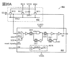
- 20A and 20B are diagrams showing a circuit configuration example of a flip-flop circuit.
- FIG. 21 is a timing chart illustrating an operation example of the CPU.
- FIG. 22 is a diagram showing a structural example of the semiconductor device.
- 23A and 23B are diagrams showing a configuration example of a transistor.
- 24A and 24B are diagrams showing a configuration example of an integrated circuit.
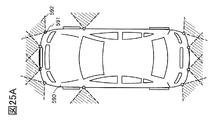
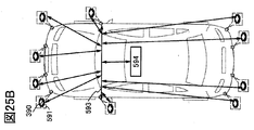
- 25A and 25B are diagrams showing application examples of integrated circuits.
- 26A and 26B are diagrams showing application examples of integrated circuits.
- 27A to 27C are diagrams illustrating an application example of an integrated circuit.
- FIG. 28 is a diagram showing an application example of an integrated circuit.
- the semiconductor device is a device utilizing semiconductor characteristics, and refers to a circuit including a semiconductor element (transistor, diode, photodiode, etc.), a device having the same circuit, and the like. It also refers to all devices that can function by utilizing semiconductor characteristics. For example, an integrated circuit, a chip having an integrated circuit, and an electronic component in which the chip is housed in a package are examples of semiconductor devices. Further, the storage device, the display device, the light emitting device, the lighting device, the electronic device, and the like are themselves semiconductor devices, and may have the semiconductor device.
- an element for example, a switch, a transistor, a capacitive element, an inductor, a resistance element, a diode, a display
- One or more devices, light emitting devices, loads, etc. can be connected between X and Y.
- the switch is controlled in an on state and an off state. That is, the switch is in a conducting state (on state) or a non-conducting state (off state), and has a function of controlling whether or not a current flows.
- X and Y are electrically connected, it means that X and Y are electrically connected (that is, another element between X and Y). Or when they are connected with another circuit in between) and when X and Y are directly connected (that is, they are connected without another element or another circuit between X and Y). If there is) and.
- circuit diagram shows that independent components are electrically connected to each other, one component has the functions of a plurality of components.
- one component has the functions of a plurality of components.
- the term "electrically connected” as used herein includes the case where one conductive film has the functions of a plurality of components in combination.
- the resistance value can be, for example, preferably 1 m ⁇ or more and 10 ⁇ or less, more preferably 5 m ⁇ or more and 5 ⁇ or less, and further preferably 10 m ⁇ or more and 1 ⁇ or less. Further, for example, it may be 1 ⁇ or more and 1 ⁇ 10 9 ⁇ or less.
- the “capacitance element” means, for example, a circuit element having a capacitance value higher than 0F, a wiring region having a capacitance value higher than 0F, a parasitic capacitance, and a transistor. It can be the gate capacitance of. Therefore, in the present specification and the like, the “capacitive element” is not only a circuit element containing a pair of electrodes and a dielectric contained between the electrodes, but also a parasitic element generated between the wirings. It shall include capacitance, gate capacitance generated between one of the source or drain of the transistor and the gate, and the like.
- the transistor has three terminals called a gate, a source, and a drain.
- the gate is a control terminal that controls the conduction state of the transistor.
- the two terminals that function as sources or drains are the input and output terminals of the transistor.
- One of the two input / output terminals becomes a source and the other becomes a drain depending on the high and low potentials given to the conductive type (n-channel type, p-channel type) of the transistor and the three terminals of the transistor. Therefore, in the present specification and the like, the terms source and drain can be paraphrased with each other.
- each gate may be referred to as a first gate, a second gate, a third gate, or the like in the present specification and the like.
- the "on state” of the transistor means a state in which the source and drain of the transistor can be regarded as being electrically short-circuited (also referred to as “conduction state”).
- the “off state” of the transistor means a state in which the source and drain of the transistor can be regarded as being electrically cut off (also referred to as a “non-conducting state”).
- the “on current” may mean a current flowing between the source and the drain when the transistor is in the on state.
- the “off current” may mean a current flowing between the source and the drain when the transistor is in the off state.
- a node can be paraphrased as a terminal, a wiring, an electrode, a conductive layer, a conductor, an impurity region, or the like, depending on a circuit configuration, a device structure, or the like.
- terminals, wiring, etc. can be paraphrased as nodes.
- ground potential ground potential
- the potentials are relative, and when the reference potential changes, the potential given to the wiring, the potential applied to the circuit or the like, the potential output from the circuit or the like also changes.
- the "current” is a charge transfer phenomenon (electrical conduction).
- the description “electrical conduction of a positively charged body is occurring” means “electrical conduction of a negatively charged body in the opposite direction”. Is happening. " Therefore, in the present specification and the like, “current” refers to a charge transfer phenomenon (electrical conduction) accompanying the movement of carriers, unless otherwise specified.
- the carrier here include electrons, holes, anions, cations, complex ions, and the like, and the carriers differ depending on the system in which the current flows (for example, semiconductor, metal, electrolyte, vacuum, etc.).
- the "current direction” in the wiring or the like shall be the direction in which the positive carrier moves, and shall be described as a positive current amount.
- the ordinal numbers “first”, “second”, and “third” are added to avoid confusion of the components. Therefore, the number of components is not limited. Moreover, the order of the components is not limited. For example, the component referred to in “first” in one of the embodiments of the present specification and the like may be the component referred to in “second” in another embodiment or in the claims. There can also be. Further, for example, the component mentioned in “first” in one of the embodiments of the present specification and the like may be omitted in another embodiment or in the claims.
- the terms “upper” and “lower” do not limit the positional relationship of the components to be directly above or directly below and to be in direct contact with each other.
- the terms “electrode B on the insulating layer A” it is not necessary that the electrode B is formed in direct contact with the insulating layer A, and another configuration is formed between the insulating layer A and the electrode B. Do not exclude those that contain elements.
- the positional relationship of the constituent elements changes as appropriate according to the direction in which each configuration is depicted. Therefore, it is not limited to the words and phrases explained in the specification and the like, and can be appropriately paraphrased according to the situation.
- terms indicating the arrangement such as “above” and “below” may be used for convenience in order to explain the positional relationship of the components with reference to the drawings. Therefore, in the expression of "insulator located on the upper surface of the conductor”, it can be rephrased as “insulator located on the lower surface of the conductor” by rotating the direction of the drawing shown by 180 degrees. Further, in the expression of "insulator located on the upper surface of the conductor”, it can be paraphrased as "insulator located on the left side (or right side) of the conductor” by rotating the direction of the drawing shown by 90 degrees. can.
- electrode B overlapping the insulating layer A is not limited to the state of "the electrode B is formed on the insulating layer A", but “the electrode B is formed under the insulating layer A”. It does not exclude the state of "being” or the state of "the electrode B is formed on the right side (or left side) of the insulating layer A”.
- the terms “adjacent” and “proximity” do not limit that the components are in direct contact with each other.
- electrode B adjacent to the insulating layer A it is not necessary that the insulating layer A and the electrode B are formed in direct contact with each other, and another component is formed between the insulating layer A and the electrode B. Do not exclude those that include.
- membrane and layer can be interchanged with each other depending on the situation.
- the terms “insulating layer” and “insulating film” may be changed to the term "insulator”.
- Electrode may be used as part of a “wiring” and vice versa.
- the terms “electrode” and “wiring” include the case where a plurality of “electrodes” and “wiring” are integrally formed.
- a “terminal” may be used as part of a “wiring” or “electrode” and vice versa.
- the term “terminal” includes a case where a plurality of "electrodes", “wiring”, “terminals” and the like are integrally formed.
- terms such as “wiring”, “signal line”, and “power supply line” can be interchanged with each other in some cases or depending on the situation.
- the reverse is also true, and it may be possible to change terms such as “signal line” and “power supply line” to the term “wiring”.
- a term such as “power line” may be changed to a term such as "signal line”.
- terms such as “signal line” may be changed to terms such as "power line”.
- the term “potential” applied to the wiring may be changed to a term such as “signal” in some cases or depending on the situation.
- the reverse is also true, and terms such as “signal” may be changed to the term “potential”.
- the switch means a switch that is in a conductive state (on state) or a non-conducting state (off state) and has a function of controlling whether or not a current flows.
- the switch means a switch having a function of selecting and switching a path through which a current flows.
- an electric switch, a mechanical switch, or the like can be used. That is, the switch is not limited to a specific switch as long as it can control the current.
- Examples of electrical switches include transistors (for example, bipolar transistors, MOS transistors, etc.), diodes (for example, PN diodes, PIN diodes, Schottky diodes, MIM (Metal Insulator Metal) diodes, and MIS (Metal Insulator Semiconductor) diodes. , Diode-connected transistors, etc.), or logic circuits that combine these.
- transistors for example, bipolar transistors, MOS transistors, etc.
- diodes for example, PN diodes, PIN diodes, Schottky diodes, MIM (Metal Insulator Metal) diodes, and MIS (Metal Insulator Semiconductor) diodes. , Diode-connected transistors, etc.
- the "conducting state" of the transistor means a state in which the source electrode and the drain electrode of the transistor can be regarded as being electrically short-circuited.
- the "non-conducting state" of the transistor means a state in which the source electrode and the drain electrode of the transistor can be regarded as being electrically cut off.
- the polarity (conductive type) of the transistor is not particularly limited.
- a mechanical switch is a switch using MEMS (Micro Electro Mechanical Systems) technology.
- the switch has an electrode that can be moved mechanically, and the movement of the electrode controls conduction and non-conduction.
- parallel means a state in which two straight lines are arranged at an angle of ⁇ 10 ° or more and 10 ° or less. Therefore, the case of ⁇ 5 ° or more and 5 ° or less is also included.
- substantially parallel or approximately parallel means a state in which two straight lines are arranged at an angle of ⁇ 30 ° or more and 30 ° or less.
- vertical means a state in which two straight lines are arranged at an angle of 80 ° or more and 100 ° or less. Therefore, the case of 85 ° or more and 95 ° or less is also included.
- substantially vertical or “approximately vertical” means a state in which two straight lines are arranged at an angle of 60 ° or more and 120 ° or less.
- a metal oxide is a metal oxide in a broad sense. Metal oxides are classified into oxide insulators, oxide conductors (including transparent oxide conductors), oxide semiconductors (also referred to as Oxide Semiconductor or simply OS) and the like. For example, when a metal oxide is used in the active layer of a transistor, the metal oxide may be referred to as an oxide semiconductor. That is, when a metal oxide can form a channel forming region of a transistor having at least one of an amplification action, a rectifying action, and a switching action, the metal oxide is referred to as a metal oxide semiconductor. be able to. Further, when describing as an OS transistor, it can be paraphrased as a transistor having a metal oxide or an oxide semiconductor.
- a metal oxide having nitrogen may also be collectively referred to as a metal oxide. Further, a metal oxide having nitrogen may be referred to as a metal oxynitride.
- the configuration shown in each embodiment can be appropriately combined with the configuration shown in other embodiments to form one aspect of the present invention. Further, when a plurality of configuration examples are shown in one embodiment, the configuration examples can be appropriately combined with each other.
- the content (may be a part of the content) described in one embodiment is the other content (may be a part of the content) described in the embodiment and one or more other implementations. It is possible to apply, combine, or replace at least one content with the content described in the form of (may be a part of the content).
- figure (which may be a part) described in one embodiment is different from another part of the figure, another figure (which may be a part) described in the embodiment, and one or more other figures.
- the figure (which may be a part) described in the embodiment is different from another part of the figure, another figure (which may be a part) described in the embodiment, and one or more other figures.
- more figures can be formed.
- the components are classified according to their functions and shown as blocks independent of each other.
- it is difficult to separate the components for each function and there may be a case where a plurality of functions are involved in one circuit or a case where one function is involved in a plurality of circuits. Therefore, the blocks in the block diagram are not limited to the components described in the specification, and can be appropriately paraphrased according to the situation.
- the size, layer thickness, or area may be exaggerated for clarity. Therefore, it is not necessarily limited to its size and aspect ratio.
- the drawings schematically show ideal examples, and are not limited to the shapes or values shown in the drawings. For example, it is possible to include variations in the signal, voltage, or current due to noise, or variations in the signal, voltage, or current due to timing lag.
- the semiconductor device 100 will be described with reference to the drawings.
- arrows indicating the X direction, the Y direction, and the Z direction may be added.
- the X, Y, and Z directions are directions that intersect each other. More specifically, the X, Y, and Z directions are directions that are orthogonal to each other.
- one of the X direction, the Y direction, and the Z direction may be referred to as a "first direction” or a "first direction”.
- the other one may be referred to as a "second direction” or a "second direction”.
- the remaining one may be referred to as a "third direction” or a "third direction”.
- the semiconductor device 100 has a plurality of arithmetic blocks 200 arranged in a matrix of M rows and N columns (M and N are two or more natural numbers, respectively).
- M and N are two or more natural numbers, respectively.
- the calculation block 200 in the first row and second column is shown as a calculation block 200 [1, 2]
- the calculation block 200 in the M row and Nth column is shown as a calculation block 200 [M, N].
- FIG. 2B shows a perspective view of the calculation block 200.
- the calculation block 200 includes a calculation circuit unit 210, a write bit line drive circuit 220, a write word line drive circuit 240, a read word line drive circuit 230, and a storage circuit unit 310.
- the arithmetic block 200 is configured by using a plurality of transistors.
- the semiconductor of the transistor included in the arithmetic block 200 a single crystal semiconductor, a polycrystalline semiconductor, a microcrystal semiconductor, an amorphous semiconductor, or the like can be used alone or in combination.
- the semiconductor material for example, silicon, germanium, or the like can be used.
- compound semiconductors such as silicon germanium, silicon carbide, gallium arsenide, oxide semiconductors, and nitride semiconductors may be used.
- the semiconductor used for the transistor may be a laminate of semiconductors.
- semiconductors having different crystal states may be laminated, or different semiconductor materials may be laminated.
- the semiconductor material used for the semiconductor in which the transistor channel is formed is appropriately used according to the purpose and / or the application.
- an OS transistor in combination with a Si transistor or other transistor depending on the purpose and / or application.
- the layer 110 includes, for example, a Si transistor
- the layer 120 includes, for example, an OS transistor.
- the arithmetic circuit unit 210, the write bit line drive circuit 220, the write word line drive circuit 240, and the read word line drive circuit 230 which are required to have an operation speed faster than that of the storage circuit, are provided on the layer 110.
- the layer 120 is provided with the storage circuit unit 310, which is required to have a smaller off current than the operating speed.
- the layer 110 includes an arithmetic circuit unit 210 having M rows and N columns. Therefore, the layer 110 may be referred to as an "arithmetic circuit array”. Further, the layer 120 includes a storage circuit unit 310 of M rows and N columns. Therefore, the layer 120 may be referred to as a "memory array”. Further, the storage circuit unit 310 may be referred to as a "memory sub-array".
- the semiconductor device 100 can be downsized. That is, since the arithmetic circuit unit 210 and the storage circuit unit 310 have a region where they overlap each other, the semiconductor device 100 can be miniaturized. Moreover, the occupied area of the semiconductor device 100 can be reduced.
- FIG. 4A is a diagram illustrating the configuration of the calculation block 200.
- the storage circuit unit 310 has a plurality of memory cells 320 arranged in a matrix of P rows and Q columns (P and Q are two or more natural numbers, respectively). Therefore, the memory array includes M ⁇ N ⁇ P ⁇ Q memory cells 320.
- the memory cell 320 in the first row and the second column is shown as the memory cell 320 [1, 2]
- the memory cell 320 in the P row and Q column is shown as the memory cell 320 [P, Q].
- the i-th (i is a natural number of 1 or more and P or less) wiring WWL and the i-th wiring RWL are electrically connected to the Q memory cells 320 arranged in the i-th row.
- the j-th wiring WBL (j is a natural number of 1 or more and Q or less) and the j-th wiring RBL are electrically connected to P memory cells 320 arranged in the j-th row.
- the memory cell 320 is electrically connected to the arithmetic circuit unit 210 via the wiring RBL. Further, the memory cell 320 is electrically connected to the write bit line drive circuit 220 via the wiring WBL. Further, the memory cell 320 is electrically connected to the read word line drive circuit 230 via the wiring RWL. Further, the memory cell 320 is electrically connected to the write word line drive circuit 240 via the wiring WWL.
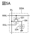
- FIG. 4B shows an example of a circuit configuration that can be used for the memory cell 320.
- the memory cell 320 illustrated in FIG. 4B has a transistor 321 and a transistor 322, and a transistor 323.
- the gate of the transistor 321 is electrically connected to the wiring WWL.
- One of the source or drain of transistor 321 is electrically connected to the wiring WBL and the other is electrically connected to the gate of transistor 322.
- One of the source or drain of transistor 322 is electrically connected to a wire that provides a fixed potential, eg, ground potential, and the other is electrically connected to one of the source or drain of transistor 323.
- the other of the source or drain of the transistor 323 is electrically connected to the wiring RBL.
- the gate of the transistor 323 is electrically connected to the wiring RWL.
- a node that electrically connects the other of the source or drain of the transistor 321 to the gate of the transistor 322 functions as a node SN.
- the node SN may be provided with a capacity of 324.
- One electrode constituting the capacitance 324 is electrically connected to the gate (node SN) of the transistor 322, and the other electrode is electrically connected to a wiring that gives a fixed potential, for example, a ground potential.
- the oxide semiconductor has a band gap of 2 eV or more, the OS transistor has a significantly small off current. Therefore, the electric charge supplied to the node SN can be retained for a long period of time. Further, the capacity 324 can be reduced or omitted. In addition, the power consumption of the semiconductor device 100 can be reduced.
- the transistor 321 When an OS transistor is used as the transistor 321 and a transistor other than the OS transistor is used for the transistor 322 and the transistor 323, the transistor 321 may be provided on the layer 120, and the transistor 322 and the transistor 323 may be provided on the layer 110.
- an OS transistor may be used for the transistor 321 and the transistor 322, and the transistor 323.
- the off-current of the OS transistor hardly increases even in a high temperature environment. Specifically, the off-current hardly increases even at an ambient temperature of room temperature or higher and 200 ° C. or lower. Further, the OS transistor has a high dielectric strength between the source and the drain. By using an OS transistor, it is possible to realize a semiconductor device having stable operation even in a high temperature environment and having good reliability.
- a memory including an OS transistor is also referred to as an "OS memory".
- the storage circuit unit 310 can be stacked directly above the arithmetic circuit unit 210.
- NOSRAM Nonvolatile Oxide Semiconductor RAM
- 2T 2-transistor type
- 3T 3-transistor type
- OS OS transistor
- the NOSRAM can function as a non-volatile memory by holding the charge corresponding to the data in the memory circuit (node SN) by using the characteristic that the off current of the OS transistor is extremely small. Further, since the NO SRAM can read the held data without destroying it (non-destructive reading), it is suitable for parallel processing of the product-sum operation of a neural network in which the data reading operation is repeated many times, for example.
- the data that can be held in the memory cell 320 is not limited to 1-bit data.
- the memory cell 320 can hold a plurality of bits of data (multi-valued data) or analog data.
- the circuit configuration that can be used for the memory cell 320 is not limited to the circuit configuration shown in FIGS. 4B and 4C.
- it may be a circuit corresponding to the DOSRAM shown in FIG. 5A.
- DOSRAM is a RAM having a 1T1C type memory cell including an OS transistor, and is an abbreviation for "Dynamic Oxide Semiconductor RAM”. Therefore, DOSRAM is a kind of OS memory.
- a flash memory an MRAM (Magnetoresistive RAM), a PRAM (Phase change RAM), a ReRAM (Resistive RAM), a FeRAM (Ferroelectric RAM), or the like may be used.
- MRAM Magneticoresistive RAM
- PRAM Phase change RAM
- ReRAM Resistive RAM
- FeRAM Feroelectric RAM
- the memory cell 320A shown in FIG. 5A has a transistor 321 and a capacitance 324.
- the transistor 321 shown in FIG. 5A is an OS transistor having a back gate.
- the memory cell 320A is electrically connected to the wiring BL, the wiring WWL, and the wiring BGL.
- the wiring BGL is electrically connected to the back gate of the transistor 321.
- the wiring BL may function as a wiring WBL or as a wiring RBL.
- the circuit configuration that can be used for the memory cell 320 may be a circuit corresponding to the 2T type NO SRAM shown in FIG. 5B.
- FIG. 5B illustrates a memory cell 320B having a transistor 321 and a transistor 322 and a capacitance 324.
- the transistor 321 and the transistor 322 shown in FIG. 5B are OS transistors.
- the transistor 321 and the transistor 322 may be an OS transistor in which both semiconductor layers are arranged in different layers, or an OS transistor in which both semiconductor layers are arranged in the same layer.
- the memory cell 320B is electrically connected to the wiring WBL, the wiring RBL, the wiring WWL, the wiring RWL, the wiring SL, and the wiring BGL.
- the wiring BGL is electrically connected to the back gate of the transistor 321.
- one electrode constituting the capacitance 324 is electrically connected to the gate of the transistor 322, and the other electrode is electrically connected to the wiring RWL.
- one of the source or drain of the transistor 322 is electrically connected to the wiring RBL, and the other is electrically connected to the wiring SL.
- the circuit configuration applicable to the memory cell 320 may be a circuit in which the 3T type NO SRAM shown in FIG. 5C is combined.
- FIG. 5C illustrates a memory cell 320C having a memory cell 320P capable of holding data having different logics and a memory cell 320N.
- Each transistor included in the memory cell 320C is an OS transistor.
- the memory cell 320P is electrically connected to the wiring WBL_P, the wiring RBL_P, the wiring WWL, and the wiring RWL.
- the memory cell 320N is electrically connected to the wiring WBL_N, the wiring RBL_N, the wiring WWL, and the wiring RWL.
- the memory cell 320P has a transistor 321P, a transistor 322P, a transistor 323P, and a capacitance 324P, and can hold information (charge) supplied to the node SNP for a long period of time.
- the memory cell 320N has a transistor 321N, a transistor 322N, a transistor 323N, and a capacity 324N, and can hold the information (charge) supplied to the node SNN for a long period of time.
- the semiconductor layers of the transistors included in the memory cell 320C may be arranged in different layers, or all of them may be arranged in the same layer. Further, a plurality of semiconductor layers may be arranged on the same layer.
- the memory cell 320C can hold data having different logics in the node SNP and the node SNN. Further, the retained data can be read out via the wiring RBL_P and the wiring RBL_N.
- an exclusive OR circuit so that the data corresponding to the multiplication of the data held in the memory cell 320P and the memory cell 320N is output to the wiring RBL (not shown in FIG. 5C).
- RBL not shown in FIG. 5C
- An arithmetic circuit for performing various arithmetic processing such as product-sum arithmetic processing, pooling arithmetic processing, normalization processing, and activation arithmetic processing can be applied to the arithmetic circuit unit 210.
- a plurality of arithmetic circuits can be provided in the arithmetic circuit unit 210. Further, the arithmetic circuit unit 210 can be provided with a plurality of types of arithmetic circuits.
- FIG. 6A shows a circuit configuration example of the arithmetic circuit 211 applicable to the arithmetic circuit unit 210.
- FIG. 6A shows an example of a circuit configuration capable of performing a product-sum operation of 8-bit weight data W and 8-bit input data A.
- the arithmetic circuit 211 shown in FIG. 6A has a multiplication circuit 24, an addition circuit 25, and a register 26.
- the input data A IN and the selected weight data W SEL is converted is multiplied by the multiplication circuit 24 into 16-bit data D M, is input to the adder circuit 25.
- the adder circuit 25, data D R, which is held in the data D M in the register 26 are added, held in the register 26 as new data D R. At this time, there are cases where the number of digits of the new data D R becomes 17 bits. Each time the above multiplication and addition are repeated, the number of digits of the new data D R may increase. Therefore, in FIG.
- FIG. 6A a circuit configuration for performing arithmetic processing using 8-bit data has been described.
- the arithmetic circuit 211 shown in FIG. 6A can also be applied to arithmetic processing performed using 1-bit data.
- the circuit configuration is shown in FIG. 6B in the same manner as in FIG. 6A. If the weight data W SEL and the input data A IN is 1-bit data, the data D M generated by the multiplying circuit 24 becomes one bit data. Since other arithmetic processes are the same as those described above, further description thereof will be omitted.
- the weight data W used in the product-sum calculation process is held in the storage circuit unit 310 provided so as to overlap the calculation circuit unit 210. Therefore, since the wiring RBL used for reading the weight data W can be shortened, the wiring resistance and the parasitic capacitance can be reduced, and high-speed reading of the weight data W can be realized. Further, the power consumption required for reading the weight data W can be reduced.
- the semiconductor device 100 since the semiconductor device 100 according to one aspect of the present invention has a read word line drive circuit 230 for each calculation block 200, it is possible to realize a higher speed read of the weight data W.
- the semiconductor device 100 since the semiconductor device 100 according to one aspect of the present invention has a write bit line drive circuit 220 and a write word line drive circuit 240 for each calculation block 200, high-speed writing of weight data W can be realized.
- FIG. 7 shows a block diagram of an arithmetic processing system 1000 including a semiconductor device 100 that functions as an AI accelerator.
- the arithmetic processing system 1000 shown in FIG. 7 includes a semiconductor device 100, a CPU 400, a bus 410, a control device 150, and a storage device 160. Further, it may have a main storage device 420, an auxiliary storage device 430, an input / output device 440, and the like.
- the control device 150, the main storage device 420, the auxiliary storage device 430, the input / output device 440, and the like are electrically connected to the CPU 400 via the bus 410.
- the CPU 400 has a CPU core 401 and a backup circuit 402. As described above, the semiconductor device 100 has a plurality of arithmetic blocks 200, but FIG. 7 shows one arithmetic block 200.
- the CPU 400 has a function of performing general-purpose processing such as execution of an operating system, data control, various operations, and program execution.
- the CPU 400 has a CPU core 401.
- the CPU core 401 corresponds to one or more CPU cores.
- the CPU 400 has a backup circuit 402 that can hold the data in the CPU core 401 even if the supply of the power supply voltage is stopped.
- the supply of the power supply voltage can be controlled by electrical disconnection from the power supply domain (power domain) by a power switch or the like.
- the power supply voltage may be referred to as a drive voltage.
- the backup circuit 402 for example, it is preferable to use an OS memory having an OS transistor.
- the backup circuit 402 composed of the OS transistor can be provided so as to be stacked with the CPU core 401 that can be composed of the Si transistor. Since the area of the backup circuit 402 is smaller than the area of the CPU core 401, the backup circuit 402 can be arranged on the CPU core 401 without increasing the circuit area.
- the backup circuit 402 has a function of holding the register data of the CPU core 401.
- the backup circuit 402 is also referred to as a data holding circuit. The details of the configuration of the CPU 400 including the backup circuit 402 having the OS transistor will be described in the third embodiment.
- the control device 150 has a function of controlling the operation of the semiconductor device 100 that functions as an AI accelerator.
- the control device 150 has a function of supplying a signal for controlling the writing and reading of the weight data W to the semiconductor device 100.
- the control device 150 has a function of giving input data A to the semiconductor device 100 and causing the semiconductor device 100 to execute a product-sum calculation of a neural network or the like.
- the control device 150 is electrically connected to the CPU 400 via the bus 410. Therefore, the semiconductor device 100 is electrically connected to the CPU 400 via the bus 410.
- the storage device 160 has a function of holding output data obtained by the semiconductor device 100, such as the product-sum calculation result of the neural network.
- a DRAM Dynamic Random Access Memory
- SRAM Static Random Access Memory
- OS memory OS memory
- the main storage device 420 has a function of storing programs and parameters related to the operation of the arithmetic processing system 1000, and it is preferable that at least a part of the main storage device 420 is a rewritable memory.
- the main storage device 420 can include a volatile memory such as a RAM (Random Access Memory) and a non-volatile memory such as a ROM (Read Only Memory).
- An OS memory may be used for the main storage device 420.
- the auxiliary storage device 430 is a storage device for storing an operating system, an application program, various data, and the like. In addition, various parameters used in the CPU 400 and the semiconductor device 100 may be stored.
- auxiliary storage device 430 for example, a storage device to which a non-volatile storage element such as a flash memory, MRAM, PRAM, ReRAM, or FeRAM is applied, or a volatile storage element such as DRAM and / or SRAM is applied.
- a storage device or the like may be used.
- a recording media drive such as a hard disk drive (Hard Disk Drive: HDD) and / or a solid state drive (Solid State Drive: SSD) may be used.
- auxiliary storage device 430 a storage device such as an HDD or SSD that can be attached and detached via the input / output device 440 may be used.
- a media drive of a recording medium such as a flash memory, a Blu-ray disc, or a DVD can also be used as the auxiliary storage device 430.
- the input / output device 440 has a function of controlling the input / output of signals between the external device and the arithmetic processing system 1000. Further, as an external port included in the input / output device 440, an HDMI (registered trademark) terminal, a USB terminal, a LAN (Local Area Network) connection terminal, or the like may be used. Further, the input / output device 440 may have a transmission / reception function for optical communication using infrared rays, visible light, ultraviolet rays, or the like.
- FIG. 8A is a block diagram illustrating a sequence of arithmetic processing.
- FIG. 8B is a diagram illustrating a data flow (flow of input data A and weight data W) of the sequence shown in FIG. 8A.
- FIG. 8B shows a data flow between the storage circuit unit 310, the arithmetic circuit unit 210, and the storage device 160.
- FIG. 8A shows an input layer 90A, an intermediate layer (also referred to as a hidden layer) 90B, and an output layer 90C.
- the input layer 90A shows an input process 92 (shown as “Input”) of input data.
- the convolution operation processing 93, the convolution operation process 94, the convolution operation process 96 (shown as “Conv.1”, “Conv.2”, “Conv.3”), the pooling operation process 95, and the pooling operation process 97 (shown as "Pool.1” and "Pool.2”) is shown.
- the output layer 90C shows a fully coupled arithmetic process 98 (shown as “Full”).
- the weight data initialization process 91 (shown as “W-Ini.” In the figure) is performed. Weighting data initialization process 91, a main storage device 420 or the auxiliary storage device 430 weight data W 1 to the weight data W 4 is held in, via the control unit 150 writes the storage circuit section 310 of the operation block 200.
- the input process 92 is performed.
- the data A 0 held in the main storage device 420 or the auxiliary storage device 430 is processed, and the data A 1 for performing the convolution calculation process 93 is generated.
- the data A 1 is stored in the storage device 160. It is also possible to use the data held in the storage device 160 as the data A 0.
- the convolution calculation process 93 is performed.
- the product-sum calculation process (MAC) is performed using the weight data W 1 and the data A 1 to generate the data A 2.
- the data A 1 is read from the storage device 160, the data A 1 is input to the calculation block 200 in which the weight data W 1 is written, and the product-sum calculation process is performed in the calculation block 200.
- the obtained data A 2 is stored in the storage device 160.
- the convolution calculation process 94 is performed.
- the product-sum calculation process is performed using the weight data W 2 and the data A 2 , and the data A 3 is generated. Similar to the convolution calculation process 93, the data A 2 is read from the storage device 160, the data A 2 is input to the calculation block 200 in which the weight data W 2 is written, and the product-sum calculation process is performed in the calculation block 200. Data A 3 obtained is held in the storage device 160.
- the pooling calculation process 95 is performed.
- the data A 3 obtained by the convolution operation processing 94, not via the storage device 160 may be directly pooling processing.
- the pooling operation processing 95 compresses the data A 3 obtained in the convolution process, deforms more manageable data (down sampling).
- the pooling operation processing may be performed by the maximum pooling. Further, as the pooling calculation process, average pooling, Lp pooling, or the like may be used. Generating data A 4 by pooling operation processing 95. Data A 4 obtained is held in the storage device 160.
- the convolution calculation process 96 is performed.
- the product-sum calculation process is performed using the weight data W 3 and the data A 4 , and the data A 5 is generated. Similar to the convolution calculation process 94, the data A 4 is read from the storage device 160, the data A 4 is input to the calculation block 200 in which the weight data W 3 is written, and the product-sum calculation process is performed in the calculation block 200. The resulting data A 5 are held in the storage device 160.
- the pooling calculation process 97 is performed.
- the data A 5 obtained by the convolution operation processing 96, not via the storage device 160 may be directly pooling processing.
- Performs pooling operation processing on the data A 5 In pooling operation processing 97 generates the data A 6.
- the resulting data A 6 is held in the storage device 160.
- the generated data A 6 is data from which the features of the data A 0 have been extracted.
- the fully combined calculation process 98 is performed. Since the data A 6 is the data obtained by extracting the features of the data A 0 , it cannot be classified or identified as it is.
- the product-sum calculation process is performed using the weight data W 4 and the data A 6 , and the data A 7 is generated. For example, by using the softmax function, it can be converted to probability of correctly classifying the data A 7 in the respective classifications.
- the flow of arithmetic processing in the input layer 90A, the intermediate layer 90B, and the output layer 90C is an example, and in the actual arithmetic processing of the convolutional neural network, other arithmetic processing may be performed.
- the arithmetic processing system 1000 including the semiconductor device 100 it is not necessary to perform the weight data initialization processing 91 again when performing the arithmetic processing of the convolutional neural network from the second time onward. Therefore, the power consumption and processing time required for the weight data initialization processing 91 can be reduced.
- the semiconductor device 100 can write and hold all the weight data W used in the arithmetic processing of the convolutional neural network in the memory array (storage circuit unit 310). Since the semiconductor device 100 according to one aspect of the present invention does not need to write the weight data W every time the product-sum calculation process (convolution calculation process, etc.) is performed, the calculation process can be speeded up.
- the semiconductor device 100 When a large weight data is supplied to the arithmetic circuit array (arithmetic circuit unit 210) via the bus 410, it is necessary to increase the bandwidth of the bus 410. Assuming that the connection via the bus 410 is a one-dimensional connection, the semiconductor device 100 according to one aspect of the present invention is provided with the arithmetic circuit unit 21 and the storage circuit unit 310 in an overlapping manner, so that a two-dimensional connection can be realized. .. That is, the semiconductor device 100 according to one aspect of the present invention can easily increase the bandwidth. Further, in the semiconductor device 100 according to one aspect of the present invention, it is easy to increase the number of parallel arithmetic circuits.
- the semiconductor device 100 according to one aspect of the present invention has a high writing speed of weight data W. Therefore, even with the arithmetic processing as shown in FIGS. 9A and 9B, high-speed arithmetic processing can be realized.
- the weight data initialization process 99 may be completed before the start of the fully combined operation 98.
- 10A and 10B show a sequence and a data flow when the weight data initialization process 99 is performed during the execution of the pooling operation process 97.
- the sequences shown in FIGS. 9 and 10 are effective when the total capacity of the weight data W (in the present embodiment, the sum of the weight data W 1 to the weight data W 4 ) is larger than the storage capacity of the memory array.
- the semiconductor device 100 can perform various arithmetic processes, not limited to the arithmetic processing of the convolutional neural network.
- FIG. 11 shows a top view of the semiconductor device 100A.
- the semiconductor device 100A is a modification of the semiconductor device 100. In order to reduce duplication of description, the differences between the semiconductor device 100A and the semiconductor device 100 will be mainly described.
- the semiconductor device 100A has a plurality of arithmetic blocks 200A arranged in a matrix of M rows and N columns (M and N are two or more natural numbers, respectively).
- the write word line drive circuit 240 and the read word line drive circuit 230 may be arranged so as to face each other with the storage circuit unit 310 in between.
- FIG. 12 shows a top view of the semiconductor device 100B.
- the semiconductor device 100B is a modification of the semiconductor device 100. In order to reduce duplication of description, the differences between the semiconductor device 100B and the semiconductor device 100 will be mainly described.
- the semiconductor device 100B includes an arithmetic block array 290 including a plurality of arithmetic blocks 200B arranged in a matrix of M rows and N columns (M and N are natural numbers of 2 or more each), a write word line drive circuit 240A, and N elements.
- the calculation block 200B includes a calculation circuit unit 210, a read word line drive circuit 230, and a storage circuit unit 310.
- the calculation block 200B has a configuration in which the write bit line drive circuit 220A and the write word line drive circuit 240 are removed from the calculation block 200.
- the storage circuit unit 310 has a memory cell 320 having P rows and Q columns. Therefore, the memory array of the semiconductor device 100B includes the memory cells 320 in the R rows and S columns. In FIG. 12, the memory cell 320 in the R row and S column is shown as the memory cell 320 [R, S]. The memory cells 320 [R, S] correspond to the memory cells [P, Q] in the calculation block 200B [M, N].
- the write word line drive circuit 240A is provided outside the arithmetic block array 290.
- the writing word line drive circuit 240A extends in the column direction and is electrically connected to the R wiring WWL extending in the row direction (Y direction).
- the g-th (g is a natural number of 1 or more and R or less) wiring WWL is electrically connected to S memory cells 320 arranged in the g-th row.
- the write word line drive circuit 240A has a function of controlling the write operation of all the arithmetic blocks 200B included in the semiconductor device 100B. For example, it has a function of controlling the operation of writing the weight data W to the storage circuit unit 310 in the calculation block 200B.
- By providing the write word line drive circuit 240A it is possible to reduce the number of M ⁇ N write word line drive circuits 240 included in the semiconductor device 100.
- the semiconductor device 100B can further reduce the occupied area as compared with the semiconductor device 100.
- N write bit line drive circuits 220A are provided outside the arithmetic block array 290.
- Each of the write bit line drive circuits 220A extends in the row direction (X direction). Further, the N write bit line drive circuits 220A are arranged in a row in the row direction. Further, each of the write bit line drive circuits 220A is arranged in each column of the calculation block 200B.
- the write bit line drive circuit 220A arranged in the first (first column) is referred to as “write bit line drive circuit 220A [1]”, and the write is arranged in the Nth (Nth column).
- the bit line drive circuit 220A is referred to as a "write bit line drive circuit 220A [N]”.
- the write bit line drive circuit 220A arranged in the e-th (e-th column) (e is a natural number of 1 or more and N or less) is indicated as “write bit line drive circuit 220A [e]”.
- calculation block 200B in the first row and e column is referred to as “calculation block 200B [1, e]”
- the calculation block 200B in the M row and e column is referred to as “calculation block 200B [M, e]”. Shown.
- the write bit line drive circuit 220A [e] is electrically connected to the arithmetic block 200B arranged in the e-th column via the Q wiring WBL extending in the column direction (Y direction).
- the write bit line drive circuit 220A [e] is electrically connected to the storage circuit unit 310 of each of the arithmetic blocks 200B arranged in the e-th column.
- the jth wiring WBL is a memory possessed by each of the arithmetic blocks 200B arranged in the e-th column. It is electrically connected to the memory cell 320 in the j-th row included in the circuit unit 310.
- the j-th wiring WBL that is electrically connected to the write bit line drive circuit 220A [e] is included in each of the calculation block 200B [1, e] to the calculation block 200B [M, e], and is included in the memory cell 320. It is electrically connected to [1, j] to the memory cell 320 [P, j].
- the write bit line drive circuit 220A [e] has a function of supplying data to all the calculation blocks 200B arranged in the e-th column. For example, it has a function of supplying weight data W to all the storage circuit units 310 arranged in the e-th column.
- the write bit line drive circuit 220A it is possible to reduce the number of M ⁇ N write bit line drive circuits 220 included in the semiconductor device 100.
- the semiconductor device 100B can further reduce the occupied area as compared with the semiconductor device 100.
- the semiconductor device 100B can reduce the occupied area as compared with the semiconductor device 100.
- the writing time of the weight data W is longer than that of the semiconductor device 100.
- the total calculation time is increased. It may occupy a small proportion. In such a case, it is preferable to use the configuration of the semiconductor device 100B.
- the writing word line drive circuit 240A When the writing word line drive circuit 240A is provided inside the arithmetic block array 290, it is preferably provided at the center or near the center of the arithmetic block 200B having N rows. For example, when N is an even number, it is preferable to provide it between the calculation block 200B in the N / 2nd column and the calculation block 200B in the (N / 2) + 1st column. When N is an odd number, it is preferable to provide it between the calculation block 200B in the (N / 2) -0.5th column and the calculation block 200B in the (N / 2) +0.5th column. Alternatively, it is preferable that the writing word line drive circuit 240A is provided adjacent to the calculation block 200B in the range of N ⁇ 0.4th column or more and N ⁇ 0.6th column or less.
- the write bit line drive circuit 220A When the write bit line drive circuit 220A is provided inside the arithmetic block array 290, it is preferably provided at the center or near the center of the arithmetic block 200B having M rows. For example, when M is an even number, it is preferable to provide it between the calculation block 200B on the M / 2nd line and the calculation block 200B on the (M / 2) + 1st line. When M is an odd number, it is preferable to provide it between the calculation block 200B on the (M / 2) -0.5 line and the calculation block 200B on the (M / 2) +0.5 line. Alternatively, it is preferable that the write bit line drive circuit 220A is provided adjacent to the calculation block 200B in the range of M ⁇ 0.4th line or more and M ⁇ 0.6th line or less.
- the maximum connection distance between the write bit wire drive circuit 220A and the arithmetic block 200B is shortened. Therefore, the maximum connection distance between the write bit line drive circuit 220A and the memory cell 320 is shortened. By shortening the maximum connection distance, effects such as reduction of power consumption, improvement of operating speed, reduction of variation, and improvement of reliability can be obtained.
- the semiconductor device 100E includes an arithmetic block array 290 including a plurality of arithmetic blocks 200C arranged in a matrix of M rows and N columns (M and N are natural numbers of 2 or more each), a write word line drive circuit 240A, and a read word. It has a line drive circuit 230A and N write bit line drive circuits 220A. Further, similarly to the semiconductor device 100B, in the semiconductor device 100E, the memory array includes memory cells 320 arranged in a matrix of R rows and S columns.
- the arithmetic block 200C has an arithmetic circuit unit 210 and a storage circuit unit 310.
- the arithmetic block 200C has a configuration in which the read word line drive circuit 230 is removed from the arithmetic block 200B.
- the read word line drive circuit 230A is provided outside the arithmetic block array 290, like the write word line drive circuit 240A.
- the readout word line drive circuit 230A extends in the column direction and is electrically connected to the R wiring RWL extending in the row direction.
- the g-th wiring RWL is electrically connected to the S memory cells 320 arranged in the g-th row.
- FIG. 16 shows a top view of the semiconductor device 100F.
- the semiconductor device 100F is a modification of the semiconductor device 100E.
- the write word line drive circuit 240A and the read word line drive circuit 230A may be provided so as to face each other with the arithmetic block array 290 interposed therebetween.
- FIG. 17 shows a top view of the semiconductor device 100G.
- the semiconductor device 100G is a modification of the semiconductor device 100E.
- the write word line drive circuit 240A and the read word line drive circuit 230A may be provided inside the arithmetic block array 290.
- the write word line drive circuit 240A and the read word line drive circuit 230A are provided inside the arithmetic block array 290, it is preferable to provide them in the center or near the center of the arithmetic block 200C having N rows. For example, when N is an even number, it is preferable to provide it between the calculation block 200C in the N / 2nd column and the calculation block 200C in the (N / 2) + 1st column. When N is an odd number, it is preferable to provide it between the calculation block 200C in the (N / 2) -0.5th column and the calculation block 200C in the (N / 2) +0.5th column. Alternatively, it is preferable that the writing word line drive circuit 240A is provided adjacent to the calculation block 200C in the range of N ⁇ 0.4th column or more and N ⁇ 0.6th column or less.
- the maximum between the write word line drive circuit 240A and the read word line drive circuit 230A and the arithmetic block 200C The connection distance becomes shorter. Therefore, the maximum connection distance between the write word line drive circuit 240A and the read word line drive circuit 230A and the memory cell 320 is shortened. By shortening the maximum connection distance, effects such as reduction of power consumption, improvement of operating speed, reduction of variation, and improvement of reliability can be obtained.
- FIG. 18 is a diagram illustrating an example of operation when a part of the calculation of the program executed by the CPU is executed by the accelerator (semiconductor device 100).
- step S1 the host program is executed by the CPU (host program execution: step S1).
- step S2 When the CPU confirms an instruction to allocate the data area required for performing the calculation using the accelerator in the memory circuit unit (storage circuit unit 310) (memory allocation instruction: step S2), the data. An area for use is secured in the memory circuit section (memory allocation: step S3).
- the CPU transmits weight data, which is input data, from the main memory or the external storage device to the memory circuit unit (data transmission: step S4).
- the memory circuit unit receives the weight data and stores the weight data in the area secured in step S2 (data reception: step S5).
- the CPU may be switched from the state of performing arithmetic to the PG (power gating) state (PG state transition: step S8). In that case, immediately before the accelerator finishes executing the kernel program, the CPU is switched from the PG state to the state of performing the calculation (PG state stop: step S9).
- PG state transition step S8
- step S9 state of performing the calculation
- step S10 When the accelerator finishes executing the kernel program, the output data is stored in the storage unit that holds the calculation result in the accelerator (completion of calculation: step S10).
- the semiconductor device of one aspect of the present invention has a non-Von Neumann architecture, and can perform arithmetic processing with extremely low power consumption as compared with the von Neumann architecture in which power consumption increases as the processing speed increases. ..
- FIG. 19 shows a configuration example of the CPU 400.
- the CPU 400 includes a CPU core (CPU Core) 401, an L1 (level 1) cache memory device (L1 Cache) 403, an L2 cache memory device (L2 Cache) 404, a bus interface unit (Bus I / F) 405, and a power switch 491 ⁇ . It has 493, a level shifter 494 (LS).
- the CPU core 401 has a flip-flop 480.
- the CPU core 401, the L1 cache memory device 403, and the L2 cache memory device 404 are connected to each other by the bus interface unit 405.
- the PMU193 generates a clock signal GCLK1 and various PG (power gating) control signals (PG control signals) in response to signals such as interrupt signals (Interrupts) input from the outside and signal SLEEP1 issued by the CPU 400.
- the clock signals GCLK1 and PG control signals are input to the CPU 400.
- the PG control signal controls the power switches 491 to 493 and the flip-flop 480.
- the power switches 491 and 492 control the supply of the voltages VDDD and VDD1 to the virtual power supply line V_VDD (hereinafter referred to as V_ VDD line), respectively.
- the power switch 493 controls the supply of the voltage VDDH to the level shifter 494.
- the voltage VSSS is input to the CPU 400 and the PMU 193 without going through the power switch.
- the voltage VDDD is input to the PMU 193 without going through the power switch.
- the voltages VDDD and VDD1 are drive voltages for CMOS circuits.
- the voltage VDD1 is lower than the voltage VDDD and is a driving voltage in the sleep state.
- the voltage VDDH is a drive voltage for the OS transistor and is higher than the voltage VDDD.
- Each of the L1 cache memory device 403, the L2 cache memory device 404, and the bus interface unit 405 has at least one power gating capable power domain.
- a power domain capable of power gating is provided with one or more power switches. These power switches are controlled by a PG control signal.
- the flip-flop 480 is used as a register.
- the flip-flop 480 is provided with a backup circuit.
- the flip-flop 480 will be described.
- FIG. 20A shows an example of a circuit configuration of a flip-flop 480 (Flip-flop).
- the flip-flop 480 has a scan flip-flop (Scan Flip-flop) 481 and a backup circuit (Backup Circuit) 402.
- FIG. 20B is a perspective view showing a circuit configuration example of the flip-flop 480.
- the scan flip-flop 481 has nodes D1, Q1, SD, SE, RT, CK, and a clock buffer circuit 481A.
- Node D1 is a data (data) input node
- node Q1 is a data output node
- node SD is a scan test data input node.
- the node SE is an input node of the signal SCE.
- the node CK is an input node for the clock signal GCLK1.
- the clock signal GCLK1 is input to the clock buffer circuit 481A.
- the analog switch of the scan flip-flop 481 is connected to the nodes CK1 and CKB1 of the clock buffer circuit 481A.
- the node RT is an input node for a reset signal.
- the signal SCE is a scan enable signal and is generated by the PMU193.
- PMU193 generates signals BK and RC.
- the level shifter 494 level-shifts the signals BK and RC to generate the signals BKH and RCH.
- the signal BK is a backup signal
- the signal RC is a recovery signal.
- the circuit configuration of the scan flip-flop 481 is not limited to FIG. Flip-flops provided in standard circuit libraries can be applied.
- the backup circuit 402 includes nodes SD_IN, SN11, transistors M11 to M13, and a capacitive element C11.
- the node SD_IN is an input node for scan test data and is connected to node Q1 of the scan flip-flop 481.
- the node SN11 is a holding node of the backup circuit 402.
- the capacitance element C11 is a holding capacitance for holding the voltage of the node SN11.
- the transistor M11 controls the conduction state between the node Q1 and the node SN11.
- the transistor M12 controls the conduction state between the node SN11 and the node SD.
- the transistor M13 controls the conduction state between the node SD_IN and the node SD.
- the on / off of the transistors M11 and M13 is controlled by the signal BKH, and the on / off of the transistors M12 is controlled by the signal RCH.
- the transistors M11 to M13 are OS transistors, like the transistors 321 to 323 of the memory cell 320 described above. Transistors M11 to M13 show a configuration having a back gate. The back gates of the transistors M11 to M13 are connected to a power supply line that supplies the voltage VBG1.
- the backup circuit 402 has a non-volatile characteristic because it can suppress a drop in the voltage of the node SN11 due to the feature of the OS transistor that the off-current is extremely small and consumes almost no power for holding data. Since the data is rewritten by charging / discharging the capacitive element C11, the backup circuit 402 is not limited in the number of rewrites in principle, and data can be written and read with low energy.
- the backup circuit 402 can be laminated on the scan flip-flop 481 composed of the silicon CMOS circuit.
- the backup circuit 402 Since the backup circuit 402 has a very small number of elements as compared with the scan flip-flop 481, it is not necessary to change the circuit configuration and layout of the scan flip-flop 481 in order to stack the backup circuits 402. That is, the backup circuit 402 is a highly versatile backup circuit. Further, since the backup circuit 402 can be provided in the region where the scan flip-flop 481 is formed, the area overhead of the flip-flop 480 can be reduced to zero even if the backup circuit 402 is incorporated. Therefore, by providing the backup circuit 402 on the flip-flop 480, power gating of the CPU core 401 becomes possible. Since the energy required for power gating is small, it is possible to power gate the CPU core 401 with high efficiency.
- the backup circuit 402 By providing the backup circuit 402, the parasitic capacitance due to the transistor M11 is added to the node Q1, but since it is smaller than the parasitic capacitance due to the logic circuit connected to the node Q1, the scan flip-flop 481 operates. There is no effect. That is, even if the backup circuit 402 is provided, the performance of the flip-flop 480 does not substantially deteriorate.
- the PMU193 when transitioning from a normal operating state to a hibernate state, the PMU193 performs voltage and / or frequency scaling. For example, when performing voltage scaling, the PMU 193 turns off the power switch 491 and turns on the power switch 492 in order to input the voltage VDD1 to the CPU core 401.
- the voltage VDD1 is a voltage that does not cause the data of the scan flip-flop 481 to be lost.
- PMU193 lowers the frequency of the clock signal GCLK1.
- FIG. 21 is a timing chart illustrating an example of the power gating sequence of the CPU core 401.
- t1 to t7 represent the time.
- the signals PSE0 to PSE2 are control signals of the power switches 491 to 493 and are generated by the PMU193. When the signal PSE0 is “H” / “L”, the power switch 491 is on / off. The same applies to the signals PSE1 and PSE2.
- the transistor M11 of the backup circuit 402 is turned on, and the data of the node Q1 of the scan flip-flop 481 is written to the node SN11 of the backup circuit 402. If the node Q1 of the scan flip-flop 481 is "L”, the node SN11 remains “L”, and if the node Q1 is "H”, the node SN11 becomes "H”.
- the PMU193 sets the signals PSE2 and BK to “L” at time t2 and sets the signal PSE0 to “L” at time t3.
- the state of the CPU core 401 shifts to the power gating state.
- the signal PSE0 may be lowered at the timing of lowering.
- the PMU 193 sets the signal PSE0 to “H” to shift from the power gating state to the recovery state.
- the PMU193 sets the signals PSE2, RC, and SCE to “H” in a state where charging of the V_ VDD line is started and the voltage of the V_ VDD line becomes VDDD (time t5).
- the transistor M12 is turned on, and the electric charge of the capacitive element C11 is distributed to the node SN 11 and the node SD. If the node SN11 is "H”, the voltage of the node SD rises. Since the node SE is “H”, the data of the node SD is written to the input side latch circuit of the scan flip-flop 481. When the clock signal GCLK1 is input to the node CK at time t6, the data of the input side latch circuit is written to the node Q1. That is, the data of the node SN11 is written to the node Q1.
- PMU193 sets the signals PSE2, SCE, and RC to “L”, and the recovery operation ends.
- the backup circuit 402 using the OS transistor is very suitable for normal off computing because it has low dynamic and static low power consumption.
- a CPU 400 including a CPU core 401 having a backup circuit 402 using an OS transistor can be referred to as a NonfCPU (registered trademark).
- the Noff CPU has a non-volatile memory and can stop the power supply when the operation is not required. Even if the flip-flop 480 is mounted, the performance of the CPU core 401 can be reduced and the dynamic power can be hardly increased.
- the CPU core 401 may have a plurality of power domains capable of power gating.
- the plurality of power domains are provided with one or more power switches for controlling the voltage input.
- the CPU core 401 may have one or more power domains in which power gating is not performed.
- a power gating control circuit for controlling the flip-flop 480 and the power switches 491 to 493 may be provided in the power domain where power gating is not performed.
- the application of the flip-flop 480 is not limited to the CPU 400.
- the flip-flop 480 can be applied to a register provided in a power domain capable of power gating.
- Embodiment 4 an example of a transistor configuration applicable to the CPU 400 and the semiconductor device 100 described in the above embodiment will be described.
- a configuration in which transistors having different electrical characteristics are laminated and provided will be described. With this configuration, the degree of freedom in designing the semiconductor device can be increased. Further, by stacking transistors having different electrical characteristics, the degree of integration of the semiconductor device can be increased.
- FIG. 22 A part of the cross-sectional structure of the semiconductor device is shown in FIG.
- the semiconductor device shown in FIG. 22 includes a transistor 550, a transistor 500, and a capacitive element 600.
- FIG. 23A is a cross-sectional view of the transistor 500 in the channel length direction
- FIG. 23B is a cross-sectional view of the transistor 500 in the channel width direction.
- the transistor 500 corresponds to an OS transistor included in the memory cell 320 shown in the above embodiment, that is, a transistor having an oxide semiconductor in a channel forming region.
- the transistor 550 corresponds to a Si transistor included in the arithmetic circuit unit 210 shown in the above embodiment, that is, a transistor having silicon in the channel forming region.
- the transistor 500 is an OS transistor.
- the OS transistor has an extremely small off current. Therefore, it is possible to hold the data voltage or electric charge written to the storage node via the transistor 500 for a long period of time. That is, since the refresh operation frequency of the storage node is reduced or the refresh operation is not required, the power consumption of the semiconductor device can be reduced.
- the transistor 500 is provided above the transistor 550, and the capacitive element 600 is provided above the transistor 550 and the transistor 500.
- the transistor 550 is provided on the substrate 371.
- the substrate 371 is, for example, a p-type silicon substrate.
- the substrate 371 may be an n-type silicon substrate.
- the oxide layer 374 is preferably an insulating layer (also referred to as a BOX layer) formed in the substrate 371 by buried oxidation, for example, silicon oxide.
- the transistor 550 is provided on a single crystal silicon, a so-called SOI (Silicon On Insulator) substrate, which is provided on the substrate 371 via an oxide layer 374.
- SOI Silicon On Insulator
- the substrate 371 of the SOI substrate is provided with an insulator 373 that functions as an element separation layer.
- the substrate 371 also has a well region 372.
- the well region 372 is a region to which n-type or p-type conductivity is imparted depending on the conductivity type of the transistor 550.
- the single crystal silicon in the SOI substrate is provided with a semiconductor region 375, a low resistance region 376a that functions as a source region or a drain region, and a low resistance region 376b. Further, a low resistance region 376c is provided on the well region 372.
- the transistor 550 can be provided so as to be superposed on the well region 372 to which the impurity element that imparts conductivity is added.
- the well region 372 can function as a bottom gate electrode of the transistor 550 by independently changing the potential via the low resistance region 376c. Therefore, the threshold voltage of the transistor 550 can be controlled.
- the threshold voltage of the transistor 550 can be made larger and the off-current can be reduced. Therefore, by applying a negative potential to the well region 372, the drain current when the potential applied to the gate electrode of the Si transistor is 0 V can be reduced.
- the power consumption based on the through current or the like in the arithmetic circuit unit 210 having the transistor 550 can be reduced, and the arithmetic efficiency can be improved.
- the transistor 550 is preferably of the so-called Fin type, in which the upper surface of the semiconductor layer and the side surface in the channel width direction are covered with the conductor 378 via the insulator 377.
- the on-characteristics of the transistor 550 can be improved by increasing the effective channel width. Further, since the contribution of the electric field of the gate electrode can be increased, the off characteristic of the transistor 550 can be improved.
- the transistor 550 may be either a p-channel type transistor or an n-channel type transistor.
- the conductor 378 may function as a first gate (also referred to as a top gate) electrode. Further, the well region 372 may function as a second gate (also referred to as a bottom gate) electrode. In that case, the potential applied to the well region 372 can be controlled via the low resistance region 376c.
- the region 376c or the like preferably contains a semiconductor such as a silicon-based semiconductor, and preferably contains single crystal silicon. Alternatively, it may be formed of a material having Ge (germanium), SiGe (silicon germanium), GaAs (gallium arsenide), GaAlAs (gallium aluminum arsenide), or the like. A configuration using silicon in which the effective mass is controlled by applying stress to the crystal lattice and changing the lattice spacing may be used. Alternatively, the transistor 550 may be a HEMT by using GaAs, GaAlAs, or the like.
- the well region 372, the low resistance region 376a, the low resistance region 376b, and the low resistance region 376c are elements that impart n-type conductivity such as arsenic and phosphorus, or boron, in addition to the semiconductor material applied to the semiconductor region 375. It contains an element that imparts p-type conductivity such as.
- the conductor 378 that functions as a gate electrode is a semiconductor material such as silicon, a metal material, or an alloy that contains an element that imparts n-type conductivity such as arsenic or phosphorus, or an element that imparts p-type conductivity such as boron.
- a material or a conductive material such as a metal oxide material can be used.
- a silicide such as nickel silicide may be used as the conductor 378.
- the threshold voltage of the transistor can be adjusted by selecting the material of the conductor. Specifically, it is preferable to use a material such as titanium nitride or tantalum nitride for the conductor. Further, in order to achieve both conductivity and embedding property, it is preferable to use a metal material such as tungsten or aluminum as a laminate for the conductor, and it is particularly preferable to use tungsten in terms of heat resistance.
- the low resistance region 376a, the low resistance region 376b, and the low resistance region 376c may be configured to be provided by laminating another conductor, for example, a silicide such as nickel silicide. With this configuration, the conductivity of the region that functions as an electrode can be enhanced. At this time, an insulator that functions as a side wall spacer (also referred to as a side wall insulating layer) may be provided on the side surface of the conductor 378 that functions as the gate electrode and the side surface of the insulator that functions as the gate insulating film. .. With this configuration, it is possible to prevent the conductor 378 and the low resistance region 376a and the low resistance region 376b from being in a conductive state.
- a silicide such as nickel silicide
- An insulator 379, an insulator 381, an insulator 383, and an insulator 385 are laminated in this order so as to cover the transistor 550.
- the insulator 379, the insulator 381, the insulator 383, and the insulator 385 for example, silicon oxide, silicon oxide nitride, silicon nitride oxide, silicon nitride, aluminum oxide, aluminum oxide nitride, aluminum nitride, etc. are used. Just do it.
- the oxidative nitride refers to a material having a higher oxygen content than nitrogen.
- silicon oxide refers to a material whose composition contains oxygen, nitrogen, and silicon and has a higher oxygen content than nitrogen.
- the nitride oxide refers to a material having a higher oxygen content than nitrogen.
- aluminum nitride refers to a material whose composition contains oxygen, nitrogen, and aluminum and has a higher nitrogen content than oxygen.
- the insulator 381 may have a function as a flattening film for flattening a step generated by a transistor 550 or the like provided below the insulator 381.
- the upper surface of the insulator 381 may be flattened by a flattening treatment using a chemical mechanical polishing (CMP) method or the like in order to improve the flatness.
- CMP chemical mechanical polishing
- the insulator 383 it is preferable to use a film having a barrier property so that hydrogen and impurities do not diffuse in the region where the transistor 500 is provided from the substrate 371 or the transistor 550.
- a film having a barrier property against hydrogen for example, silicon nitride formed by the CVD method can be used.
- hydrogen may diffuse into a semiconductor element having an oxide semiconductor such as a transistor 500, so that the characteristics of the semiconductor element may deteriorate. Therefore, it is preferable to use a film that suppresses the diffusion of hydrogen between the transistor 500 and the transistor 550.
- the membrane that suppresses the diffusion of hydrogen is a membrane that desorbs a small amount of hydrogen.
- the amount of hydrogen desorbed can be analyzed using, for example, a heated desorption gas analysis method (TDS).
- TDS heated desorption gas analysis method
- the amount of hydrogen desorbed from the insulator 383 is such that the amount desorbed in terms of hydrogen atoms is converted per area of the insulator 383 when the surface temperature of the film is in the range of 50 ° C. to 500 ° C. It may be 10 ⁇ 10 15 atoms / cm 2 or less, preferably 5 ⁇ 10 15 atoms / cm 2 or less.
- the insulator 385 preferably has a lower dielectric constant than the insulator 383.
- the relative permittivity of the insulator 385 is preferably less than 4, more preferably less than 3.
- the relative permittivity of the insulator 385 is preferably 0.7 times or less, more preferably 0.6 times or less, the relative permittivity of the insulator 383.
- the insulator 379, the insulator 381, the insulator 383, and the insulator 385 are embedded with a capacitance element 600, a conductor 328 connected to the transistor 500, a conductor 330, and the like.
- the conductor 328 and the conductor 330 have a function as a plug or a wiring.
- the conductor having a function as a plug or a wiring may collectively give a plurality of configurations and give the same reference numeral.
- the wiring and the plug connected to the wiring may be integrated. That is, a part of the conductor may function as a wiring, and a part of the conductor may function as a plug.
- each plug and wiring As the material of each plug and wiring (conductor 328, conductor 330, etc.), a conductive material such as a metal material, an alloy material, a metal nitride material, or a metal oxide material is used as a single layer or laminated. be able to. It is preferable to use a refractory material such as tungsten and / or molybdenum that has both heat resistance and conductivity, and it is preferable to use tungsten. Alternatively, it is preferably formed of a low resistance conductive material such as aluminum and / or copper. Wiring resistance can be reduced by using a low resistance conductive material.
- a conductive material such as a metal material, an alloy material, a metal nitride material, or a metal oxide material is used as a single layer or laminated. be able to. It is preferable to use a refractory material such as tungsten and / or molybdenum that has both heat resistance and conductivity, and it is preferable
- a wiring layer may be provided on the insulator 385 and the conductor 330.
- the insulator 350, the insulator 352, and the insulator 354 are laminated in this order.
- a conductor 356 is formed on the insulator 350, the insulator 352, and the insulator 354.
- the conductor 356 has a function as a plug or wiring for connecting to the transistor 550.
- the conductor 356 can be provided by using the same materials as the conductor 328 and the conductor 330.
- the insulator 350 it is preferable to use an insulator having a barrier property against hydrogen, similarly to the insulator 383.
- the conductor 356 preferably contains a conductor having a barrier property against hydrogen.
- a conductor having a barrier property against hydrogen is formed in the opening of the insulator 350 having a barrier property against hydrogen.
- the conductor having a barrier property against hydrogen for example, tantalum nitride or the like may be used. Further, by laminating tantalum nitride and tungsten having high conductivity, it is possible to suppress the diffusion of hydrogen from the transistor 550 while maintaining the conductivity as wiring. In this case, it is preferable that the tantalum nitride layer having a barrier property against hydrogen is in contact with the insulator 350 having a barrier property against hydrogen.
- a wiring layer may be provided on the insulator 354 and the conductor 356.
- the insulator 360, the insulator 362, and the insulator 364 are laminated in this order.
- a conductor 366 is formed in the insulator 360, the insulator 362, and the insulator 364.
- the conductor 366 has a function as a plug or wiring.
- the conductor 366 can be provided by using the same materials as the conductor 328 and the conductor 330.
- a wiring layer may be provided on the insulator 364 and the conductor 366.
- the insulator 370, the insulator 369, and the insulator 368 are laminated in this order.
- a conductor 376 is formed on the insulator 370, the insulator 369, and the insulator 368.
- the conductor 376 has a function as a plug or wiring.
- the conductor 376 can be provided by using the same materials as the conductor 328 and the conductor 330.
- the insulator 370 it is preferable to use an insulator having a barrier property against hydrogen, similarly to the insulator 383.
- the conductor 376 preferably contains a conductor having a barrier property against hydrogen.
- a conductor having a barrier property against hydrogen is formed in the opening of the insulator 370 having a barrier property against hydrogen.
- a wiring layer may be provided on the insulator 368 and the conductor 376.
- the insulator 380, the insulator 382, and the insulator 384 are laminated in this order.
- a conductor 386 is formed on the insulator 380, the insulator 382, and the insulator 384.
- the conductor 386 has a function as a plug or wiring.
- the conductor 386 can be provided by using the same materials as the conductor 328 and the conductor 330.
- the insulator 380 it is preferable to use an insulator having a barrier property against hydrogen, similarly to the insulator 383.
- the conductor 386 preferably contains a conductor having a barrier property against hydrogen.
- a conductor having a barrier property against hydrogen is formed in the opening of the insulator 380 having a barrier property against hydrogen.
- the semiconductor device according to the present embodiment has been described. It is not limited to this.
- the number of wiring layers similar to the wiring layer containing the conductor 356 may be three or less, or the number of wiring layers similar to the wiring layer containing the conductor 356 may be five or more.
- An insulator 510, an insulator 512, an insulator 514, and an insulator 516 are laminated in this order on the insulator 384.
- any of the insulator 510, the insulator 512, the insulator 514, and the insulator 516 it is preferable to use a substance having a barrier property against oxygen and hydrogen.
- the insulator 510 and the insulator 514 it is preferable to use a film having a barrier property against hydrogen and impurities in the region where the transistor 500 is provided, for example, from the region where the substrate 371 or the transistor 550 is provided. Therefore, the same material as the insulator 383 can be used.
- silicon nitride formed by the CVD method can be used as an example of a film having a barrier property against hydrogen.
- hydrogen may diffuse into a semiconductor element having an oxide semiconductor such as a transistor 500, so that the characteristics of the semiconductor element may deteriorate. Therefore, it is preferable to use a film that suppresses the diffusion of hydrogen between the transistor 500 and the transistor 550.
- the film having a barrier property against hydrogen for example, it is preferable to use metal oxides such as aluminum oxide, hafnium oxide, and tantalum oxide for the insulator 510 and the insulator 514.
- metal oxides such as aluminum oxide, hafnium oxide, and tantalum oxide for the insulator 510 and the insulator 514.
- aluminum oxide has a high blocking effect that does not allow the membrane to permeate both oxygen and impurities such as hydrogen and water that cause fluctuations in the electrical characteristics of the transistor. Therefore, aluminum oxide can prevent impurities such as hydrogen and moisture from being mixed into the transistor 500 during and after the manufacturing process of the transistor. In addition, it is possible to suppress the release of oxygen from the oxides constituting the transistor 500. Therefore, it is suitable for use as a protective film for the transistor 500.
- the same material as the insulator 379 can be used for the insulator 512 and the insulator 516. Further, by applying a material having a relatively low dielectric constant to these insulators, it is possible to reduce the parasitic capacitance generated between the wirings.
- a silicon oxide film and / or a silicon nitride film can be used as the insulator 512 and the insulator 516.
- the insulator 510, the insulator 512, the insulator 514, and the insulator 516 are embedded with a conductor 518, a conductor (for example, a conductor 503) constituting the transistor 500, and the like.
- the conductor 518 has a function as a plug or wiring for connecting to the capacitance element 600 or the transistor 550.
- the conductor 518 can be provided by using the same material as the conductor 328 and the conductor 330.
- the conductor 510 and the conductor 518 in the region in contact with the insulator 514 are preferably conductors having a barrier property against oxygen, hydrogen, and water.
- the transistor 550 and the transistor 500 can be separated by a layer having a barrier property against oxygen, hydrogen, and water, and the diffusion of hydrogen from the transistor 550 to the transistor 500 can be suppressed.
- a transistor 500 is provided above the insulator 516.
- the transistor 500 includes a conductor 503 arranged so as to be embedded in the insulator 514 and the insulator 516, and an insulator 520 arranged on the insulator 516 and the insulator 503.
- the insulator 524 placed on the insulator 522, the oxide 530a placed on the insulator 524, and the oxide 530a.
- the arranged oxide 530b, the conductors 542a and 542b arranged apart from each other on the oxide 530b, and the conductors 542a and 542b are arranged between the conductors 542a and 542b.
- It has an insulator 580 on which an opening is formed by superimposing, an insulator 545 arranged on the bottom surface and side surfaces of the opening, and a conductor 560 arranged on the forming surface of the insulator 545.
- the insulator 544 is arranged between the oxide 530a, the oxide 530b, the conductor 542a, and the conductor 542b and the insulator 580.
- the conductor 560 includes a conductor 560a provided inside the insulator 545 and a conductor 560b provided so as to be embedded inside the conductor 560a. It is preferable to have.
- the insulator 574 is arranged on the insulator 580, the conductor 560, and the insulator 545.
- the transistor 500 shows a configuration in which two layers of oxide 530a and oxide 530b are laminated in a region where a channel is formed and in the vicinity thereof, but the present invention is not limited to this.
- a single layer of the oxide 530b or a laminated structure of three or more layers may be provided.
- the conductor 560 is shown as a two-layer laminated structure, but the present invention is not limited to this.
- the conductor 560 may have a single-layer structure or a laminated structure of three or more layers.
- the transistor 500 shown in FIGS. 22, 23A, and 23B is an example, and the transistor 500 is not limited to the configuration, and an appropriate transistor may be used depending on the circuit configuration and / or the driving method.
- the conductor 560 functions as a gate electrode of the transistor, and the conductor 542a and the conductor 542b function as a source electrode or a drain electrode, respectively.
- the conductor 560 is formed so as to be embedded in the opening of the insulator 580 and the region sandwiched between the conductor 542a and the conductor 542b.
- the arrangement of the conductor 560, the conductor 542a and the conductor 542b is self-aligned with respect to the opening of the insulator 580. That is, in the transistor 500, the gate electrode can be arranged in a self-aligned manner between the source electrode and the drain electrode. Therefore, since the conductor 560 can be formed without providing the alignment margin, the occupied area of the transistor 500 can be reduced. As a result, the semiconductor device can be miniaturized and highly integrated.
- the conductor 560 is formed in a region between the conductor 542a and the conductor 542b in a self-aligned manner, the conductor 560 does not have a region that overlaps with the conductor 542a or the conductor 542b. Thereby, the parasitic capacitance formed between the conductor 560 and the conductors 542a and 542b can be reduced. Therefore, the switching speed of the transistor 500 can be improved and a high frequency characteristic can be provided.
- the conductor 560 may function as a first gate (also referred to as a top gate) electrode. Further, the conductor 503 may function as a second gate (also referred to as a bottom gate) electrode.
- the threshold voltage of the transistor 500 can be controlled by changing the potential applied to the conductor 503 independently of the potential applied to the conductor 560 without interlocking with the potential applied to the conductor 560. In particular, by applying a negative potential to the conductor 503, the threshold voltage of the transistor 500 can be made larger and the off-current can be reduced. Therefore, when a negative potential is applied to the conductor 503, the drain current when the potential applied to the conductor 560 is 0 V can be made smaller than when it is not applied.
- the conductor 503 is arranged so as to overlap the oxide 530 and the conductor 560. As a result, when a potential is applied to the conductor 560 and the conductor 503, the electric field generated from the conductor 560 and the electric field generated from the conductor 503 are connected to cover the channel forming region formed in the oxide 530. Can be done.
- the configuration of the transistor that electrically surrounds the channel formation region by the electric field of the pair of gate electrodes is referred to as a curved channel (S-channel) configuration.
- S-channel configuration disclosed in the present specification and the like is different from the Fin type configuration and the planar type configuration.
- the conductor 503 has the same structure as the conductor 518, and the conductor 503a is formed in contact with the inner wall of the opening of the insulator 514 and the insulator 516, and the conductor 503b is further formed inside.
- the transistor 500 shows a configuration in which the conductor 503a and the conductor 503b are laminated, the present invention is not limited to this.
- the conductor 503 may be provided as a single layer or a laminated structure having three or more layers.
- the conductor 503a it is preferable to use a conductive material having a function of suppressing the diffusion of impurities such as hydrogen atoms, hydrogen molecules, water molecules, and copper atoms (the above impurities are difficult to permeate).
- a conductive material having a function of suppressing the diffusion of oxygen for example, at least one oxygen atom, oxygen molecule, etc.
- the function of suppressing the diffusion of impurities or oxygen is a function of suppressing the diffusion of any one or all of the above impurities or the above oxygen.
- the conductor 503a since the conductor 503a has a function of suppressing the diffusion of oxygen, it is possible to prevent the conductor 503b from being oxidized and the conductivity from being lowered.
- the insulator 520, the insulator 522, and the insulator 524 have a function as a second gate insulating film.
- the insulator 524 in contact with the oxide 530 it is preferable to use an insulator containing more oxygen than oxygen satisfying the stoichiometric composition.
- the oxygen is easily released from the membrane by heating.
- oxygen released by heating may be referred to as "excess oxygen”. That is, it is preferable that the insulator 524 is formed with a region containing excess oxygen (also referred to as “excess oxygen region”).
- the defective (hereinafter sometimes referred to as V O H) serves as a donor, sometimes electrons serving as carriers are generated.
- a part of hydrogen may be combined with oxygen that is bonded to a metal atom to generate an electron as a carrier. Therefore, a transistor using an oxide semiconductor containing a large amount of hydrogen tends to have a normally-on characteristic. Further, since hydrogen in the oxide semiconductor easily moves due to stress such as heat and electric field, if the oxide semiconductor contains a large amount of hydrogen, the reliability of the transistor may deteriorate.
- the V O H to obtain a sufficiently reduced oxide semiconductor, the moisture in the oxide semiconductor, to remove impurities such as hydrogen (also referred to as “dewatering” or “dehydrogenation process") It is important to supply oxygen to the oxide semiconductor to compensate for the oxygen deficiency (also referred to as “oxygenation treatment").
- the V O H oxide semiconductor impurity is sufficiently reduced such by using a channel formation region of the transistor, it is possible to have stable electrical characteristics.
- an oxide material in which a part of oxygen is desorbed by heating is 1.0 ⁇ 10 18 atoms / cm 3 or more, preferably 1 in TDS (Thermal Desorption Spectroscopy) analysis.
- the surface temperature of the film during the TDS analysis is preferably in the range of 100 ° C. or higher and 700 ° C. or lower, or 100 ° C. or higher and 400 ° C. or lower.
- the insulator having the excess oxygen region and the oxide 530 may be brought into contact with each other to perform one or more of heat treatment, microwave treatment, or RF treatment.
- heat treatment microwave treatment, or RF treatment.
- water or hydrogen in the oxide 530 can be removed.
- reactions occur which bonds VoH is disconnected, when other words happening reaction of "V O H ⁇ Vo + H", it can be dehydrogenated.
- the hydrogen generated as oxygen combines with H 2 O, it may be removed from the oxide 530 or oxide 530 near the insulator.
- a part of hydrogen may be gettered to the conductor 542a and the conductor 542b.
- the microwave processing for example, it is preferable to use an apparatus having a power source for generating high-density plasma or an apparatus having a power source for applying RF to the substrate side.
- an apparatus having a power source for generating high-density plasma for example, by using a gas containing oxygen and using a high-density plasma, high-density oxygen radicals can be generated, and by applying RF to the substrate side, the oxygen radicals generated by the high-density plasma can be generated.
- the pressure may be 133 Pa or more, preferably 200 Pa or more, and more preferably 400 Pa or more.
- oxygen and argon are used as the gas to be introduced into the apparatus for performing microwave treatment, and the oxygen flow rate ratio (O 2 / (O 2 + Ar)) is 50% or less, preferably 10% or more and 30. It is better to do it at% or less.
- the heat treatment may be performed, for example, at 100 ° C. or higher and 450 ° C. or lower, more preferably 350 ° C. or higher and 400 ° C. or lower.
- the heat treatment is performed in an atmosphere of nitrogen gas or an inert gas, or an atmosphere containing 10 ppm or more, 1% or more, or 10% or more of an oxidizing gas.
- the heat treatment is preferably performed in an oxygen atmosphere.
- oxygen can be supplied to the oxide 530 to reduce oxygen deficiency (VO ).
- the heat treatment may be performed in a reduced pressure state.
- the heat treatment may be carried out in an atmosphere containing 10 ppm or more, 1% or more, or 10% or more of an oxidizing gas in order to supplement the desorbed oxygen after the heat treatment in an atmosphere of nitrogen gas or an inert gas. good.
- the heat treatment may be performed in an atmosphere containing 10 ppm or more, 1% or more, or 10% or more of the oxidizing gas, and then the heat treatment may be continuously performed in an atmosphere of nitrogen gas or an inert gas.
- the insulator 524 has an excess oxygen region, it is preferable that the insulator 522 has a function of suppressing the diffusion of oxygen (for example, oxygen atom, oxygen molecule, etc.) (the oxygen is difficult to permeate).
- oxygen for example, oxygen atom, oxygen molecule, etc.
- the insulator 522 has a function of suppressing the diffusion of oxygen and impurities, the oxygen contained in the oxide 530 does not diffuse to the insulator 520 side, which is preferable. Further, it is possible to suppress the conductor 503 from reacting with the oxygen contained in the insulator 524 and / or the oxide 530.
- the insulator 522 may be, for example, aluminum oxide, hafnium oxide, an oxide containing aluminum and hafnium (hafnium aluminate), tantalum oxide, zirconium oxide, lead zirconate titanate (PZT), strontium titanate (SrTIO 3 ), or It is preferable to use an insulator containing a so-called high-k material such as (Ba, Sr) TiO 3 (BST) in a single layer or in a laminated manner. As transistors become finer and more integrated, problems such as leakage current may occur due to the thinning of the gate insulating film. By using a high-k material for the insulator that functions as a gate insulating film, it is possible to reduce the gate potential during transistor operation while maintaining the physical film thickness.
- a so-called high-k material such as (Ba, Sr) TiO 3 (BST)
- an insulator containing an oxide of one or both of aluminum and hafnium which are insulating materials having a function of suppressing diffusion of impurities and oxygen (the above-mentioned oxygen is difficult to permeate).
- the insulator containing one or both oxides of aluminum and hafnium it is preferable to use aluminum oxide, hafnium oxide, an oxide containing aluminum and hafnium (hafnium aluminate) and the like.
- the insulator 522 releases oxygen from the oxide 530 and / or mixes impurities such as hydrogen from the peripheral portion of the transistor 500 into the oxide 530. It functions as a suppressing layer.
- aluminum oxide, bismuth oxide, germanium oxide, niobium oxide, silicon oxide, titanium oxide, tungsten oxide, yttrium oxide, and zirconium oxide may be added to these insulators.
- these insulators may be nitrided. Silicon oxide, silicon oxide nitride, or silicon nitride may be laminated on the above insulator.
- the insulator 520, the insulator 522, and the insulator 524 are shown as the second gate insulating film having a three-layer laminated structure, but the second gate.
- the insulating film may have a single layer, two layers, or a laminated structure of four or more layers. In that case, the laminated structure is not limited to the same material, and may be a laminated structure made of different materials.
- the transistor 500 uses a metal oxide that functions as an oxide semiconductor for the oxide 530 containing the channel forming region.
- oxide 530 In-M-Zn oxide (element M is aluminum, gallium, yttrium, copper, vanadium, beryllium, boron, titanium, iron, nickel, germanium, zirconium, molybdenum, lantern, cerium, neodymium).
- Hafnium, tantalum, tungsten, gallium, etc. (one or more) and the like may be used.
- the metal oxide that functions as an oxide semiconductor may be formed by a sputtering method or an ALD (Atomic Layer Deposition) method.
- ALD Atomic Layer Deposition
- the metal oxide that functions as a channel forming region in the oxide 530 it is preferable to use a metal oxide having a band gap of 2 eV or more, preferably 2.5 eV or more. In this way, by using a metal oxide having a large bandgap, the off-current of the transistor can be reduced.
- the oxide 530 can suppress the diffusion of impurities into the oxide 530b from the composition formed below the oxide 530a.
- the oxide 530 preferably has a laminated structure of a plurality of oxide layers having different atomic number ratios of each metal atom.
- the atomic number ratio of the element M in the constituent elements is larger than the atomic number ratio of the element M in the constituent elements in the metal oxide used in the oxide 530b. Is preferable.
- the atomic number ratio of the element M to In is preferably larger than the atomic number ratio of the element M to In in the metal oxide used for the oxide 530b.
- the atomic number ratio of In to the element M is preferably larger than the atomic number ratio of In to the element M in the metal oxide used for the oxide 530a.
- the energy at the lower end of the conduction band of the oxide 530a is higher than the energy at the lower end of the conduction band of the oxide 530b.
- the electron affinity of the oxide 530a is smaller than the electron affinity of the oxide 530b.
- the energy level at the lower end of the conduction band changes gently.
- the energy level at the lower end of the conduction band at the junction of the oxide 530a and the oxide 530b is continuously changed or continuously bonded. In order to do so, it is preferable to reduce the defect level density of the mixed layer formed at the interface between the oxide 530a and the oxide 530b.
- the oxide 530a and the oxide 530b have a common element (main component) other than oxygen, a mixed layer having a low defect level density can be formed.
- the oxide 530b is an In-Ga-Zn oxide
- a conductor 542a and a conductor 542b that function as a source electrode and a drain electrode are provided on the oxide 530b.
- the conductors 542a and 542b include aluminum, chromium, copper, silver, gold, platinum, tantalum, nickel, titanium, molybdenum, tungsten, hafnium, vanadium, niobium, manganese, magnesium, zirconium, beryllium, indium, and ruthenium.
- Iridium, strontium, lanthanum, or an alloy containing the above-mentioned metal element as a component, or an alloy in which the above-mentioned metal element is combined is preferably used.
- tantalum nitride, titanium nitride, tungsten, nitrides containing titanium and aluminum, nitrides containing tantalum and aluminum, ruthenium oxide, ruthenium nitride, oxides containing strontium and ruthenium, oxides containing lanthanum and nickel, etc. are used. Is preferable.
- tantalum nitride, titanium nitride, nitrides containing titanium and aluminum, nitrides containing tantalum and aluminum, ruthenium oxide, ruthenium nitride, oxides containing strontium and ruthenium, and oxides containing lanthanum and nickel are difficult to oxidize.
- a metal nitride film such as tantalum nitride is preferable because it has a barrier property against hydrogen or oxygen.
- the conductor 542a and the conductor 542b are shown as a single-layer structure, but a laminated structure of two or more layers may be used.
- a tantalum nitride film and a tungsten film may be laminated.
- the titanium film and the aluminum film may be laminated.
- a two-layer structure in which an aluminum film is laminated on a tungsten film a two-layer structure in which a copper film is laminated on a copper-magnesium-aluminum alloy film, a two-layer structure in which a copper film is laminated on a titanium film, and a two-layer structure in which a copper film is laminated on a titanium film. It may have a two-layer structure in which copper films are laminated.
- a transparent conductive material containing indium oxide, tin oxide or zinc oxide may be used.
- a region 543a and a region 543b may be formed as low resistance regions at the interface of the oxide 530 with the conductor 542a (conductor 542b) and its vicinity.
- the region 543a functions as one of the source region or the drain region
- the region 543b functions as the other of the source region or the drain region.
- a channel forming region is formed in a region sandwiched between the region 543a and the region 543b.
- the oxygen concentration in the region 543a (region 543b) may be reduced. Further, in the region 543a (region 543b), a metal compound layer containing the metal contained in the conductor 542a (conductor 542b) and the component of the oxide 530 may be formed. In such a case, the carrier density of the region 543a (region 543b) increases, and the region 543a (region 543b) becomes a low resistance region.
- the insulator 544 is provided so as to cover the conductor 542a and the conductor 542b, and suppresses the oxidation of the conductor 542a and the conductor 542b. At this time, the insulator 544 may be provided so as to cover the side surface of the oxide 530 and come into contact with the insulator 524.
- insulator 544 a metal oxide containing one or more selected from hafnium, aluminum, gallium, yttrium, zirconium, tungsten, titanium, tantalum, nickel, germanium, neodymium, lanthanum, magnesium, etc. Can be used. Further, as the insulator 544, silicon nitride oxide, silicon nitride or the like can also be used.
- the insulator 544 it is preferable to use aluminum or an oxide containing one or both oxides of hafnium, such as aluminum oxide, hafnium oxide, aluminum, and an oxide containing hafnium (hafnium aluminate). ..
- hafnium aluminate has higher heat resistance than the hafnium oxide film. Therefore, it is preferable because it is difficult to crystallize in the heat treatment in the subsequent step.
- the conductors 542a and 542b are materials having oxidation resistance or materials whose conductivity does not significantly decrease even if oxygen is absorbed, the insulator 544 is not an essential configuration. It may be appropriately designed according to the desired transistor characteristics.
- the insulator 544 By having the insulator 544, it is possible to prevent impurities such as water and hydrogen contained in the insulator 580 from diffusing into the oxide 530b. In addition, oxidation of the conductor 542a and / or the conductor 542b due to excess oxygen contained in the insulator 580 can be suppressed.
- the insulator 545 functions as a first gate insulating film.
- the insulator 545 is preferably formed by using an insulator that contains excess oxygen and releases oxygen by heating, similarly to the above-mentioned insulator 524.
- silicon oxide with excess oxygen silicon oxide, silicon nitride, silicon nitride, silicon oxide with fluorine, silicon oxide with carbon, carbon, silicon oxide with nitrogen, and pores.
- Silicon oxide having can be used.
- silicon oxide and silicon nitride nitride are preferable because they are stable against heat.
- the insulator containing excess oxygen as the insulator 545, oxygen can be effectively supplied from the insulator 545 to the channel forming region of the oxide 530b. Further, similarly to the insulator 524, it is preferable that the concentration of impurities such as water or hydrogen in the insulator 545 is reduced.
- the film thickness of the insulator 545 is preferably 1 nm or more and 20 nm or less. Further, the above-mentioned microwave treatment may be performed before and / or after the formation of the insulator 545.
- a metal oxide may be provided between the insulator 545 and the conductor 560.
- the metal oxide preferably suppresses oxygen diffusion from the insulator 545 to the conductor 560.
- the diffusion of excess oxygen from the insulator 545 to the conductor 560 is suppressed. That is, it is possible to suppress a decrease in the amount of excess oxygen supplied to the oxide 530.
- oxidation of the conductor 560 due to excess oxygen can be suppressed.
- a material that can be used for the insulator 544 may be used.
- the insulator 545 may have a laminated structure as in the case of the second gate insulating film.
- an insulator that functions as a gate insulating film is made of a high-k material and heat.
- the conductor 560 functioning as the first gate electrode is shown as a two-layer structure in FIGS. 23A and 23B, it may have a single-layer structure or a laminated structure of three or more layers.
- Conductor 560a is a hydrogen atom, a hydrogen molecule, a water molecule, a nitrogen atom, a nitrogen molecule, nitric oxide molecule (N 2 O, NO, etc. NO 2), conductive having a function of suppressing the diffusion of impurities such as copper atoms It is preferable to use a material. Alternatively, it is preferable to use a conductive material having a function of suppressing the diffusion of oxygen (for example, at least one oxygen atom, oxygen molecule, etc.). Since the conductor 560a has a function of suppressing the diffusion of oxygen, it is possible to prevent the conductor 560b from being oxidized by the oxygen contained in the insulator 545 to reduce the conductivity.
- the conductive material having a function of suppressing the diffusion of oxygen for example, tantalum, tantalum nitride, ruthenium, ruthenium oxide and the like are preferably used.
- an oxide semiconductor applicable to the oxide 530 can be used as the conductor 560a. In that case, by forming the conductor 560b into a film by a sputtering method, the electric resistance value of the conductor 560a can be lowered to form a conductor. This can be called an OC (Oxide Conductor) electrode.
- the insulator 580 is provided on the conductor 542a and the conductor 542b via the insulator 544.
- the insulator 580 preferably has an excess oxygen region.
- silicon, resin, or the like silicon oxide and silicon oxide nitride are preferable because they are thermally stable.
- silicon oxide and silicon oxide having pores are preferable because an excess oxygen region can be easily formed in a later step.
- the insulator 580 preferably has an excess oxygen region. By providing the insulator 580 in which oxygen is released by heating, the oxygen in the insulator 580 can be efficiently supplied to the oxide 530. It is preferable that the concentration of impurities such as water and hydrogen in the insulator 580 is reduced.
- the opening of the insulator 580 is formed so as to overlap the region between the conductor 542a and the conductor 542b.
- the conductor 560 is formed so as to be embedded in the opening of the insulator 580 and the region sandwiched between the conductor 542a and the conductor 542b.
- the conductor 560 may have a shape having a high aspect ratio.
- the conductor 560 is provided so as to be embedded in the opening of the insulator 580, even if the conductor 560 has a shape having a high aspect ratio, the conductor 560 is formed without collapsing during the process. Can be done.
- the insulator 574 is preferably provided in contact with the upper surface of the insulator 580, the upper surface of the conductor 560, and the upper surface of the insulator 545.
- an excess oxygen region can be provided in the insulator 545 and the insulator 580. Thereby, oxygen can be supplied into the oxide 530 from the excess oxygen region.
- the insulator 574 use one or more metal oxides selected from hafnium, aluminum, gallium, yttrium, zirconium, tungsten, titanium, tantalum, nickel, germanium, magnesium and the like. Can be done.
- aluminum oxide has a high barrier property and can suppress the diffusion of hydrogen and nitrogen even in a thin film of 0.5 nm or more and 3.0 nm or less. Therefore, the aluminum oxide formed by the sputtering method can have a function as a barrier film for impurities such as hydrogen as well as an oxygen supply source.
- the insulator 581 that functions as an interlayer film on the insulator 574.
- the insulator 581 preferably has a reduced concentration of impurities such as water and hydrogen in the film.
- the conductor 540a and the conductor 540b are arranged in the openings formed in the insulator 581, the insulator 574, the insulator 580, and the insulator 544.
- the conductor 540a and the conductor 540b are provided so as to face each other with the conductor 560 interposed therebetween.
- the conductor 540a and the conductor 540b have the same configuration as the conductor 546 and the conductor 548 described later.
- An insulator 582 is provided on the insulator 581.
- the insulator 582 it is preferable to use a substance having a barrier property against oxygen and hydrogen. Therefore, the same material as the insulator 514 can be used for the insulator 582.
- a metal oxide such as aluminum oxide, hafnium oxide, and tantalum oxide for the insulator 582.
- aluminum oxide has a high blocking effect that does not allow the membrane to permeate both oxygen and impurities such as hydrogen and water that cause fluctuations in the electrical characteristics of the transistor. Therefore, aluminum oxide can prevent impurities such as hydrogen and moisture from being mixed into the transistor 500 during and after the manufacturing process of the transistor. In addition, it is possible to suppress the release of oxygen from the oxides constituting the transistor 500. Therefore, it is suitable for use as a protective film for the transistor 500.
- the insulator 520, the insulator 522, the insulator 524, the insulator 544, the insulator 580, the insulator 574, the insulator 581, the insulator 582, and the insulator 586 include the conductor 546 and the conductor 548. Is embedded.
- the conductor 546 and the conductor 548 have a function as a plug or wiring for connecting to the capacitive element 600, the transistor 500, or the transistor 550.
- the conductor 546 and the conductor 548 can be provided by using the same materials as the conductor 328 and the conductor 330.
- an opening may be formed so as to surround the transistor 500, and an insulator having a high barrier property to hydrogen or water may be formed so as to cover the opening.
- an insulator having a high barrier property to hydrogen or water
- a plurality of transistors 500 may be put together and wrapped with an insulator having a high barrier property against hydrogen or water.
- the conductor 612 may be provided on the conductor 546 and the conductor 548.
- the conductor 612 has a function as a plug or wiring for connecting to the transistor 500.
- the conductor 610 has a function as an electrode of the capacitive element 600.
- the conductor 612 and the conductor 610 can be formed at the same time.
- the conductor 612 and the conductor 610 include a metal film containing an element selected from molybdenum, titanium, tantalum, tungsten, aluminum, copper, chromium, neodymium, and scandium, or a metal nitride film containing the above-mentioned elements as components.
- a metal nitride film, titanium nitride film, molybdenum nitride film, tungsten nitride film and the like can be used.
- indium tin oxide, indium oxide containing tungsten oxide, indium zinc oxide containing tungsten oxide, indium oxide containing titanium oxide, indium tin oxide containing titanium oxide, indium zinc oxide, and silicon oxide are added. It is also possible to apply a conductive material such as indium tin oxide.
- the conductor 612 and the conductor 610 are shown in a single-layer configuration, but the configuration is not limited to this, and a laminated configuration of two or more layers may be used.
- a conductor having a barrier property and a conductor having a high adhesion to a conductor having a high conductivity may be formed between a conductor having a barrier property and a conductor having a high conductivity.
- the conductor 620 is provided so as to overlap the conductor 610 via the insulator 630.
- a conductive material such as a metal material, an alloy material, or a metal oxide material can be used. It is preferable to use a refractory material such as tungsten and / or molybdenum which has both heat resistance and conductivity, and it is particularly preferable to use tungsten. When it is formed at the same time as other configurations such as a conductor, Cu (copper) and / or Al (aluminum), which are low resistance metal materials, may be used.
- An insulator 640 is provided on the conductor 620 and the insulator 630.
- the insulator 640 can be provided by using the same material as the insulator 379. Further, the insulator 640 may function as a flattening film that covers the uneven shape below the insulator 640.
- FIG. 24A is an example of a schematic diagram for explaining an integrated circuit including each configuration included in the arithmetic processing system 1000.
- the integrated circuit 390 illustrated in FIG. 24A can be made into one integrated circuit in which each circuit is integrated by forming a part of the circuit included in the accelerator described as the CPU 400 and the semiconductor device 100 with an OS transistor.
- a control device 150 a storage device 160, and the like can be provided.
- the storage device 160 in addition to SRAM and DRAM including Si transistors, NOSRAM and DOSRAM described in the above embodiment can be applied. Further, MRAM, PRAM, ReRAM, FeRAM and the like may be used as the storage device 160.
- the memory density can be improved by stacking the layer having the OS transistor on the drive circuit provided in the layer having the Si transistor.
- FIG. 24B shows an example of a semiconductor chip incorporating an integrated circuit 390.
- the semiconductor chip 391 shown in FIG. 24B has a lead 392 and an integrated circuit 390.
- the integrated circuit 390 is provided with various circuits shown in the above-described embodiment on one die.
- the integrated circuit 390 has a laminated structure and is roughly classified into a layer having a Si transistor (Si transistor layer 393), a wiring layer 394, and a layer having an OS transistor (OS transistor layer 395). Since the OS transistor layer 395 can be provided by being laminated on the Si transistor layer 393, the semiconductor chip 391 can be easily miniaturized.
- QFP Quad Flat Package
- Other configuration examples include insert-mounted DIP (Dual In-line Package), PGA (Pin Grid Array), surface-mounted SOP (Small Outline Package), SSOP (Shrink Small Online Package), and SSOP (Shrink Small Online Package). Thin-Small Outline Package), LCC (Leaded Chip Carrier), QFN (Quad Flat Non-leaded package), BGA (Ball Grid Array), FBGA (Fine Grid Type), FBGA (Fine Grid), FBGA (Fine Grid) Structures such as Package) and QTP (Quad Type-carrier Package) can be appropriately used.
- the arithmetic circuit and drive circuit having the Si transistor and the memory circuit having the OS transistor can all be formed in the Si transistor layer 393, the wiring layer 394, and the OS transistor layer 395. That is, the elements constituting the semiconductor device can be formed by the same manufacturing process. Therefore, in the semiconductor chip 391 shown in FIG. 24B, it is not necessary to increase the manufacturing process even if the number of constituent elements increases, and the semiconductor device can be incorporated at low cost.
- FIG. 25A illustrates an external view of an automobile as an example of a moving body.
- FIG. 25B is a diagram simplifying the exchange of data in the automobile.
- the automobile 590 has a plurality of cameras 591 and the like. Further, the automobile 590 is equipped with various sensors (not shown) such as an infrared radar, a millimeter wave radar, and a laser radar.
- the integrated circuit 390 (or the semiconductor chip 391 incorporating the integrated circuit 390) can be used in the camera 591 or the like.
- the camera 591 processes a plurality of images obtained in a plurality of imaging directions 592 by the integrated circuit 390 described in the above embodiment, and the plurality of images are collected by the host controller 594 or the like via the bus 593 or the like. By analyzing this, it is possible to determine the surrounding traffic conditions such as the presence or absence of guard rails and / or pedestrians, and perform automatic driving. It can also be used in systems for road guidance, danger prediction, and the like.
- the obtained image data is subjected to arithmetic processing such as a neural network to increase the resolution of the image, reduce image noise, face recognition (for crime prevention, etc.), and object recognition (for automatic driving).
- arithmetic processing such as a neural network to increase the resolution of the image, reduce image noise, face recognition (for crime prevention, etc.), and object recognition (for automatic driving).
- Etc. image compression, image correction (wide dynamic range), image restoration of lensless image sensor, positioning, character recognition, reduction of reflection reflection, etc. can be performed.
- moving objects include trains, monorails, ships, flying objects (helicopters, unmanned aerial vehicles (drones), airplanes, rockets), etc.
- computer of one aspect of the present invention is applied to these moving objects. Therefore, a system using artificial intelligence can be provided.
- FIG. 26A is an external view showing an example of a portable electronic device.
- FIG. 26B is a diagram simplifying the exchange of data in the portable electronic device.
- the portable electronic device 595 includes a printed wiring board 596, a speaker 597, a camera 598, a microphone 599, and the like.
- the integrated circuit 390 can be provided on the printed wiring board 596.
- the portable electronic device 595 improves user convenience by processing and analyzing a plurality of data obtained by the speaker 597, the camera 598, the microphone 599, etc. by using the integrated circuit 390 described in the above embodiment. be able to. It can also be used in systems that perform voice guidance, image search, and the like.
- the obtained image data is subjected to arithmetic processing such as a neural network to increase the resolution of the image, reduce image noise, face recognition (for crime prevention, etc.), and object recognition (for automatic driving).
- arithmetic processing such as a neural network to increase the resolution of the image, reduce image noise, face recognition (for crime prevention, etc.), and object recognition (for automatic driving).
- Etc. image compression, image correction (wide dynamic range), image restoration of lensless image sensor, positioning, character recognition, reduction of reflection reflection, etc. can be performed.
- FIG. 27B is a USB connection type stick-type electronic device 1120.
- the electronic device 1120 has a housing 1121, a cap 1122, a USB connector 1123, and a substrate 1124.
- the board 1124 is housed in the housing 1121.
- a memory chip 1125 and a controller chip 1126 are attached to the substrate 1124.
- the integrated circuit 390 shown in the previous embodiment can be incorporated into the controller chip 1126 or the like of the substrate 1124.
- FIG. 27C is a humanoid robot 1130.
- the robot 1130 has sensors 2101 to 2106 and a control circuit 2110.
- the integrated circuit 390 shown in the previous embodiment can be incorporated in the control circuit 2110.
- the integrated circuit 390 described in the above embodiment can be used as a server that communicates with the electronic device instead of being built in the electronic device.
- the computing system is composed of electronic devices and servers.
- FIG. 28 shows a configuration example of the system 3000.
- the system 3000 is composed of an electronic device 3001 and a server 3002. Communication between the electronic device 3001 and the server 3002 can be performed via the Internet line 3003.
- the server 3002 has a plurality of racks 3004.
- a plurality of substrates 3005 are provided in the plurality of racks, and the integrated circuit 390 described in the above embodiment can be mounted on the substrate 3005.
- a neural network is configured on the server 3002.
- the server 3002 can perform the calculation of the neural network by using the data input from the electronic device 3001 via the Internet line 3003.
- the result of the calculation by the server 3002 can be transmitted to the electronic device 3001 via the Internet line 3003, if necessary. Thereby, the burden of calculation in the electronic device 3001 can be reduced.
Abstract
Description
図2図2Aおよび図2Bは、半導体装置の構成を示す斜視図である。
図3は、半導体装置の構成を示す斜視図である。
図4Aは、演算ブロックの構成を説明する図である。図4Bおよび図4Cは、メモリセルの回路構成例を示す図である。
図5A乃至図5Cは、メモリセルの回路構成例を示す図である。
図6Aおよび図6Bは、演算回路の回路構成例を示す図である。
図7は、演算処理システムの構成例を示すブロック図である。
図8Aは、演算処理のシーケンスを説明するブロック図である。図8Bは、演算処理におけるデータフローを説明する図である。
図9Aは、演算処理のシーケンスを説明するブロック図である。図9Bは、演算処理におけるデータフローを説明する図である。
図10Aは、演算処理のシーケンスを説明するブロック図である。図10Bは、演算処理におけるデータフローを説明する図である。
図11は、半導体装置の変形例を示す図である。
図12は、半導体装置の変形例を示す図である。
図13は、半導体装置の変形例を示す図である。
図14は、半導体装置の変形例を示す図である。
図15は、半導体装置の変形例を示す図である。
図16は、半導体装置の変形例を示す図である。
図17は、半導体装置の変形例を示す図である。
図18は、演算処理システムの動作例を説明する図である。
図19は、CPUの構成例を示す図である。
図20Aおよび図20Bは、フリップフロップ回路の回路構成例を示す図である。
図21は、CPUの動作例を説明するタイミングチャートである。
図22は、半導体装置の構造例を示す図である。
図23Aおよび図23Bは、トランジスタの構成例を示す図である。
図24Aおよび図24Bは、集積回路の構成例を示す図である。
図25Aおよび図25Bは、集積回路の適用例を示す図である。
図26Aおよび図26Bは、集積回路の適用例を示す図である。
図27A乃至図27Cは、集積回路の適用例を説明する図である。
図28は、集積回路の適用例を示す図である。
本発明の一形態に係る半導体装置100について図面を用いて説明する。なお、図面において、X方向、Y方向、およびZ方向を示す矢印を付す場合がある。X方向、Y方向、およびZ方向は、それぞれが互いに交差する方向である。より具体的には、X方向、Y方向、およびZ方向は、それぞれが互いに直交する方向である。本明細書などでは、X方向、Y方向、またはZ方向の1つを「第1方向」または「第1の方向」と呼ぶ場合がある。また、他の1つを「第2方向」または「第2の方向」と呼ぶ場合がある。また、残りの1つを「第3方向」または「第3の方向」と呼ぶ場合がある。
図1に半導体装置100の上面図を示す。図2Aに半導体装置100の斜視図を示す。
半導体装置100は、アクセラレータとしての機能を有する。具体的には、ホストプログラムから呼び出されたプログラム(カーネル、またはカーネルプログラムとも呼ばれる)を実行する機能を有する。半導体装置100は、例えば、グラフィック処理における行列演算の並列処理、ニューラルネットワークの積和演算の並列処理、科学技術計算における浮動小数点演算の並列処理などを行うことができる。
半導体装置100は、M行N列(M、Nはそれぞれ2以上の自然数)のマトリクス状に配置された複数の演算ブロック200を有する。図1では、1行2列目の演算ブロック200を演算ブロック200[1,2]と示し、M行N列目の演算ブロック200を演算ブロック200[M,N]と示している。
図4Bに、メモリセル320に用いることができる回路構成例を示す。図4Bに例示するメモリセル320は、トランジスタ321、トランジスタ322、およびトランジスタ323を有する。トランジスタ321のゲートは配線WWLと電気的に接続される。トランジスタ321のソースまたはドレインの一方は配線WBLと電気的に接続され、他方はトランジスタ322のゲートと電気的に接続される。トランジスタ322のソースまたはドレインの一方は固定電位たとえばグラウンド電位を与える配線と電気的に接続され、他方はトランジスタ323のソースまたはドレインの一方と電気的に接続される。トランジスタ323のソースまたはドレインの他方は配線RBLと電気的に接続される。トランジスタ323のゲートは配線RWLと電気的に接続される。トランジスタ321のソースまたはドレインの他方と、トランジスタ322のゲートが電気的に接続する節点がノードSNとして機能する。
演算回路部210には、積和演算処理、プーリング演算処理、ノーマライズ処理、活性化演算処理などの様々な演算処理を行うための演算回路が適用可能である。演算回路部210には複数個の演算回路を設けることができる。また、演算回路部210には複数種類の演算回路を設けることができる。図6Aに、演算回路部210に適用できる演算回路211の回路構成例を示す。図6Aでは、8ビットの重みデータWと8ビットの入力データAの積和演算を行うことができる回路構成例を示している。
図7に、AIアクセラレータとして機能する半導体装置100を含む演算処理システム1000のブロック図を示す。
図8Aおよび図8Bを用いて、畳み込みニューラルネットワークの演算処理の一例を示す。図8Aは、演算処理のシーケンスを説明するブロック図である。図8Bは、図8Aに示すシーケンスのデータフロー(入力データAおよび重みデータWの流れ)を説明する図である。図8Bでは、記憶回路部310、演算回路部210、および記憶装置160間のデータフローを示している。
図11に半導体装置100Aの上面図を示す。半導体装置100Aは半導体装置100の変形例である。説明の重複を減らすため、半導体装置100Aの半導体装置100と異なる点について主に説明する。
図12に半導体装置100Bの上面図を示す。半導体装置100Bは半導体装置100の変形例である。説明の重複を減らすため、半導体装置100Bの半導体装置100と異なる点について主に説明する。
図13に半導体装置100Cの上面図を示す。半導体装置100Cは、半導体装置100Bの変形例である。半導体装置100Cのように、書き込みワード線駆動回路240Aを、演算ブロックアレイ290の内側に設けてもよい。
図14に半導体装置100Dの上面図を示す。半導体装置100Dは、半導体装置100Bの変形例である。半導体装置100Dのように、書き込みビット線駆動回路220Aを、演算ブロックアレイ290の内側に設けてもよい。
図15に半導体装置100Eの上面図を示す。半導体装置100Eは、半導体装置100Bの変形例である。説明の重複を減らすため、半導体装置100Eの半導体装置100Bと異なる点について主に説明する。
図16に半導体装置100Fの上面図を示す。半導体装置100Fは、半導体装置100Eの変形例である。図16に示す半導体装置100Fのように、書き込みワード線駆動回路240Aおよび読み出しワード線駆動回路230Aを、演算ブロックアレイ290を挟んで向かい合うように設けてもよい。
図17に半導体装置100Gの上面図を示す。半導体装置100Gは、半導体装置100Eの変形例である。半導体装置100Gのように、書き込みワード線駆動回路240Aおよび読み出しワード線駆動回路230Aを、演算ブロックアレイ290の内側に設けてもよい。
本実施の形態では、上記実施の形態で説明したCPU400で実行するプログラムの演算の一部をアクセラレータとして機能する半導体装置100で実行する場合の、動作の一例を説明する。
本実施の形態では、パワーゲーティングが可能なCPUコアを有するCPUの一例について説明する。
本実施の形態では、上記実施の形態で説明したCPU400、および半導体装置100に適用可能なトランジスタの構成の一例について説明する。一例として、異なる電気特性を有するトランジスタを積層して設ける構成について説明する。当該構成とすることで、半導体装置の設計自由度を高めることができる。また、異なる電気特性を有するトランジスタを積層して設けることで、半導体装置の集積度を高めることができる。
本実施の形態では、上記実施の形態で説明した演算処理システム1000が有する各構成を含む集積回路の構成について図24A、図24Bを参照しながら説明する。
本実施の形態では、上記実施の形態で説明した集積回路390を適用することが可能な電子機器、移動体、演算システムについて、図25A乃至図28を参照しながら説明する。
Claims (22)
- 複数の演算ブロックを有し、
前記演算ブロックは、
演算回路部と、記憶回路部と、を有し、
前記演算回路部は、第1トランジスタを有し、
前記記憶回路部は、第2トランジスタを有し、
前記演算回路部は前記記憶回路部と電気的に接続され、
前記演算回路部と前記記憶回路部は、互いに重なる領域を有する半導体装置。 - 請求項1において、
前記演算ブロックは、
第1駆動回路と、第2駆動回路と、第3駆動回路と、を有し、
前記第1駆動回路、前記第2駆動回路、および前記第3駆動回路は、
前記記憶回路部と電気的に接続され、
前記演算回路部、前記第1駆動回路、前記第2駆動回路、および前記第3駆動回路は、第1層に設けられ、
前記記憶回路部は第2層に設けられ、
前記第1層と前記第2層は互いに重なる領域を有する半導体装置。 - 請求項2において、
前記第1駆動回路は、前記記憶回路部にデータを供給する機能を有する半導体装置。 - 請求項2または請求項3において、
前記第2駆動回路は、前記記憶回路部にデータを書き込む動作を制御する機能を有する半導体装置。 - 請求項2乃至請求項4のいずれか一項において、
前記第3駆動回路は、前記記憶回路部からデータを読み出す動作を制御する機能を有する半導体装置。 - 請求項1乃至請求項5のいずれか一項において、
前記演算回路部は、積和演算を行う機能を有する半導体装置。 - 請求項1乃至請求項6のいずれか一項において、
前記記憶回路部は、データを保持する機能を有する半導体装置。 - 請求項7において、
前記データは重みデータである半導体装置。 - 請求項1乃至請求項8のいずれか一項において、
前記第1トランジスタは、チャネルが形成される半導体にシリコンを含む、半導体装置。 - 請求項1乃至請求項5のいずれか一項において、
前記第2トランジスタは、チャネルが形成される半導体に酸化物半導体を含む、半導体装置。 - 請求項10において、
前記酸化物半導体は、インジウムまたは亜鉛の少なくとも一方を含む、半導体装置。 - M行N列(M、Nはそれぞれ2以上の自然数)のマトリクス状に設けられた複数の演算ブロックと、N個の第1駆動回路と、を有する半導体装置であって、
前記N個の第1駆動回路は、それぞれが各列に配置され、
前記複数の演算ブロックのそれぞれは、
演算回路部と、記憶回路部と、を有し、
前記演算回路部は、前記記憶回路部と電気的に接続され、
前記演算回路部と前記記憶回路部は、互いに重なる領域を有し、
e列目(eは1以上N以下の自然数)に配置された前記記憶回路部は、
e列目に配置された前記第1駆動回路と電気的に接続される半導体装置。 - 請求項12において、
前記演算回路部は、積和演算を行う機能を有する半導体装置。 - 請求項12または請求項13において、
前記記憶回路部は、データを保持する機能を有する半導体装置。 - 請求項14において、
前記データは重みデータである半導体装置。 - 請求項12乃至請求項14のいずれか一項において、
前記記憶回路部は、複数のメモリセルを有し、
前記メモリセルは、
チャネルが形成される半導体に酸化物半導体を含むトランジスタを有する半導体装置。 - 請求項12乃至請求項16のいずれか一項において、
前記第1駆動回路は、前記記憶回路部にデータを供給する機能を有する半導体装置。 - 請求項12乃至請求項17のいずれか一項において、
列方向に延在する第2駆動回路を有し、
前記第2駆動回路は、
前記記憶回路部と電気的に接続する半導体装置。 - 請求項18において、
前記第2駆動回路は、前記記憶回路部にデータを書き込む動作を制御する機能を有する半導体装置。 - 請求項12乃至請求項19のいずれか一項において、
前記複数の演算ブロックのそれぞれは、
第3駆動回路を有し、
前記第3駆動回路は、
前記記憶回路部と電気的に接続する半導体装置。 - 請求項12乃至請求項19のいずれか一項において、
列方向に延在する第3駆動回路を有し、
前記第3駆動回路は、
前記記憶回路部と電気的に接続する半導体装置。 - 請求項20または請求項21において、
前記第3駆動回路は、前記記憶回路部からデータを読み出す動作を制御する機能を有する半導体装置。
Priority Applications (4)
| Application Number | Priority Date | Filing Date | Title |
|---|---|---|---|
| JP2022508602A JPWO2021186279A1 (ja) | 2020-03-18 | 2021-03-04 | |
| KR1020227035369A KR20220155329A (ko) | 2020-03-18 | 2021-03-04 | 반도체 장치 |
| US17/802,281 US20230099168A1 (en) | 2020-03-18 | 2021-03-04 | Semiconductor device |
| CN202180022121.4A CN115298824A (zh) | 2020-03-18 | 2021-03-04 | 半导体装置 |
Applications Claiming Priority (2)
| Application Number | Priority Date | Filing Date | Title |
|---|---|---|---|
| JP2020-047259 | 2020-03-18 | ||
| JP2020047259 | 2020-03-18 |
Publications (1)
| Publication Number | Publication Date |
|---|---|
| WO2021186279A1 true WO2021186279A1 (ja) | 2021-09-23 |
Family
ID=77768028
Family Applications (1)
| Application Number | Title | Priority Date | Filing Date |
|---|---|---|---|
| PCT/IB2021/051788 WO2021186279A1 (ja) | 2020-03-18 | 2021-03-04 | 半導体装置 |
Country Status (5)
| Country | Link |
|---|---|
| US (1) | US20230099168A1 (ja) |
| JP (1) | JPWO2021186279A1 (ja) |
| KR (1) | KR20220155329A (ja) |
| CN (1) | CN115298824A (ja) |
| WO (1) | WO2021186279A1 (ja) |
Citations (5)
| Publication number | Priority date | Publication date | Assignee | Title |
|---|---|---|---|---|
| JP2012256822A (ja) * | 2010-09-14 | 2012-12-27 | Semiconductor Energy Lab Co Ltd | 記憶装置及び半導体装置 |
| JP2015188071A (ja) * | 2014-03-14 | 2015-10-29 | 株式会社半導体エネルギー研究所 | 半導体装置 |
| JP2019033233A (ja) * | 2017-08-10 | 2019-02-28 | 株式会社半導体エネルギー研究所 | 半導体装置、および電子機器 |
| JP2019036280A (ja) * | 2017-08-11 | 2019-03-07 | 株式会社半導体エネルギー研究所 | グラフィックスプロセッシングユニット、コンピュータ、電子機器及び並列計算機 |
| JP2019047006A (ja) * | 2017-09-05 | 2019-03-22 | 株式会社半導体エネルギー研究所 | 半導体装置、電子機器 |
Family Cites Families (1)
| Publication number | Priority date | Publication date | Assignee | Title |
|---|---|---|---|---|
| US10607135B2 (en) | 2017-10-19 | 2020-03-31 | General Electric Company | Training an auto-encoder on a single class |
-
2021
- 2021-03-04 WO PCT/IB2021/051788 patent/WO2021186279A1/ja active Application Filing
- 2021-03-04 US US17/802,281 patent/US20230099168A1/en active Pending
- 2021-03-04 KR KR1020227035369A patent/KR20220155329A/ko active Search and Examination
- 2021-03-04 CN CN202180022121.4A patent/CN115298824A/zh active Pending
- 2021-03-04 JP JP2022508602A patent/JPWO2021186279A1/ja active Pending
Patent Citations (5)
| Publication number | Priority date | Publication date | Assignee | Title |
|---|---|---|---|---|
| JP2012256822A (ja) * | 2010-09-14 | 2012-12-27 | Semiconductor Energy Lab Co Ltd | 記憶装置及び半導体装置 |
| JP2015188071A (ja) * | 2014-03-14 | 2015-10-29 | 株式会社半導体エネルギー研究所 | 半導体装置 |
| JP2019033233A (ja) * | 2017-08-10 | 2019-02-28 | 株式会社半導体エネルギー研究所 | 半導体装置、および電子機器 |
| JP2019036280A (ja) * | 2017-08-11 | 2019-03-07 | 株式会社半導体エネルギー研究所 | グラフィックスプロセッシングユニット、コンピュータ、電子機器及び並列計算機 |
| JP2019047006A (ja) * | 2017-09-05 | 2019-03-22 | 株式会社半導体エネルギー研究所 | 半導体装置、電子機器 |
Also Published As
| Publication number | Publication date |
|---|---|
| US20230099168A1 (en) | 2023-03-30 |
| JPWO2021186279A1 (ja) | 2021-09-23 |
| CN115298824A (zh) | 2022-11-04 |
| KR20220155329A (ko) | 2022-11-22 |
Similar Documents
| Publication | Publication Date | Title |
|---|---|---|
| WO2018178793A1 (ja) | 半導体装置、半導体装置の作製方法 | |
| JP7361730B2 (ja) | 記憶装置 | |
| KR102496132B1 (ko) | 기억 장치 | |
| JP2023164563A (ja) | 半導体装置 | |
| WO2021234500A1 (ja) | 半導体装置 | |
| WO2021064502A1 (ja) | 半導体装置 | |
| WO2021186279A1 (ja) | 半導体装置 | |
| WO2021130591A1 (ja) | 半導体装置 | |
| WO2022013677A1 (ja) | 半導体装置 | |
| WO2021198841A1 (ja) | 半導体装置 | |
| WO2021165779A1 (ja) | 半導体装置 | |
| WO2023199182A1 (ja) | 半導体装置 | |
| WO2024013604A1 (ja) | 半導体装置 | |
| WO2021209858A1 (ja) | 半導体装置 | |
| WO2023223126A1 (ja) | 半導体装置 | |
| KR20230070233A (ko) | 반도체 장치 및 전자 기기 | |
| KR20230071139A (ko) | 반도체 장치 및 전자 기기 | |
| JP2023152817A (ja) | 半導体装置 | |
| KR20230043924A (ko) | 반도체 장치의 구동 방법 | |
| JP2018180975A (ja) | 半導体装置 |
Legal Events
| Date | Code | Title | Description |
|---|---|---|---|
| 121 | Ep: the epo has been informed by wipo that ep was designated in this application |
Ref document number: 21772566 Country of ref document: EP Kind code of ref document: A1 |
|
| ENP | Entry into the national phase |
Ref document number: 2022508602 Country of ref document: JP Kind code of ref document: A |
|
| ENP | Entry into the national phase |
Ref document number: 20227035369 Country of ref document: KR Kind code of ref document: A |
|
| NENP | Non-entry into the national phase |
Ref country code: DE |
|
| 122 | Ep: pct application non-entry in european phase |
Ref document number: 21772566 Country of ref document: EP Kind code of ref document: A1 |