WO2021182047A1 - 半導体装置 - Google Patents
半導体装置 Download PDFInfo
- Publication number
- WO2021182047A1 WO2021182047A1 PCT/JP2021/005929 JP2021005929W WO2021182047A1 WO 2021182047 A1 WO2021182047 A1 WO 2021182047A1 JP 2021005929 W JP2021005929 W JP 2021005929W WO 2021182047 A1 WO2021182047 A1 WO 2021182047A1
- Authority
- WO
- WIPO (PCT)
- Prior art keywords
- region
- pad
- semiconductor device
- main surface
- lead
- Prior art date
- Legal status (The legal status is an assumption and is not a legal conclusion. Google has not performed a legal analysis and makes no representation as to the accuracy of the status listed.)
- Ceased
Links
Images











Classifications
-
- H—ELECTRICITY
- H10—SEMICONDUCTOR DEVICES; ELECTRIC SOLID-STATE DEVICES NOT OTHERWISE PROVIDED FOR
- H10W—GENERIC PACKAGES, INTERCONNECTIONS, CONNECTORS OR OTHER CONSTRUCTIONAL DETAILS OF DEVICES COVERED BY CLASS H10
- H10W70/00—Package substrates; Interposers; Redistribution layers [RDL]
- H10W70/40—Leadframes
- H10W70/421—Shapes or dispositions
-
- H—ELECTRICITY
- H10—SEMICONDUCTOR DEVICES; ELECTRIC SOLID-STATE DEVICES NOT OTHERWISE PROVIDED FOR
- H10W—GENERIC PACKAGES, INTERCONNECTIONS, CONNECTORS OR OTHER CONSTRUCTIONAL DETAILS OF DEVICES COVERED BY CLASS H10
- H10W70/00—Package substrates; Interposers; Redistribution layers [RDL]
- H10W70/40—Leadframes
- H10W70/456—Materials
- H10W70/457—Materials of metallic layers on leadframes
-
- H—ELECTRICITY
- H10—SEMICONDUCTOR DEVICES; ELECTRIC SOLID-STATE DEVICES NOT OTHERWISE PROVIDED FOR
- H10W—GENERIC PACKAGES, INTERCONNECTIONS, CONNECTORS OR OTHER CONSTRUCTIONAL DETAILS OF DEVICES COVERED BY CLASS H10
- H10W70/00—Package substrates; Interposers; Redistribution layers [RDL]
- H10W70/40—Leadframes
- H10W70/464—Additional interconnections in combination with leadframes
- H10W70/465—Bumps or wires
-
- H—ELECTRICITY
- H10—SEMICONDUCTOR DEVICES; ELECTRIC SOLID-STATE DEVICES NOT OTHERWISE PROVIDED FOR
- H10W—GENERIC PACKAGES, INTERCONNECTIONS, CONNECTORS OR OTHER CONSTRUCTIONAL DETAILS OF DEVICES COVERED BY CLASS H10
- H10W70/00—Package substrates; Interposers; Redistribution layers [RDL]
- H10W70/40—Leadframes
- H10W70/481—Leadframes for devices being provided for in groups H10D8/00 - H10D48/00
-
- H—ELECTRICITY
- H10—SEMICONDUCTOR DEVICES; ELECTRIC SOLID-STATE DEVICES NOT OTHERWISE PROVIDED FOR
- H10W—GENERIC PACKAGES, INTERCONNECTIONS, CONNECTORS OR OTHER CONSTRUCTIONAL DETAILS OF DEVICES COVERED BY CLASS H10
- H10W74/00—Encapsulations, e.g. protective coatings
- H10W74/10—Encapsulations, e.g. protective coatings characterised by their shape or disposition
- H10W74/111—Encapsulations, e.g. protective coatings characterised by their shape or disposition the semiconductor body being completely enclosed
-
- H—ELECTRICITY
- H10—SEMICONDUCTOR DEVICES; ELECTRIC SOLID-STATE DEVICES NOT OTHERWISE PROVIDED FOR
- H10W—GENERIC PACKAGES, INTERCONNECTIONS, CONNECTORS OR OTHER CONSTRUCTIONAL DETAILS OF DEVICES COVERED BY CLASS H10
- H10W74/00—Encapsulations, e.g. protective coatings
- H10W74/10—Encapsulations, e.g. protective coatings characterised by their shape or disposition
- H10W74/111—Encapsulations, e.g. protective coatings characterised by their shape or disposition the semiconductor body being completely enclosed
- H10W74/127—Encapsulations, e.g. protective coatings characterised by their shape or disposition the semiconductor body being completely enclosed characterised by arrangements for sealing or adhesion
-
- H—ELECTRICITY
- H10—SEMICONDUCTOR DEVICES; ELECTRIC SOLID-STATE DEVICES NOT OTHERWISE PROVIDED FOR
- H10W—GENERIC PACKAGES, INTERCONNECTIONS, CONNECTORS OR OTHER CONSTRUCTIONAL DETAILS OF DEVICES COVERED BY CLASS H10
- H10W70/00—Package substrates; Interposers; Redistribution layers [RDL]
- H10W70/40—Leadframes
- H10W70/421—Shapes or dispositions
- H10W70/424—Cross-sectional shapes
-
- H—ELECTRICITY
- H10—SEMICONDUCTOR DEVICES; ELECTRIC SOLID-STATE DEVICES NOT OTHERWISE PROVIDED FOR
- H10W—GENERIC PACKAGES, INTERCONNECTIONS, CONNECTORS OR OTHER CONSTRUCTIONAL DETAILS OF DEVICES COVERED BY CLASS H10
- H10W72/00—Interconnections or connectors in packages
- H10W72/071—Connecting or disconnecting
- H10W72/075—Connecting or disconnecting of bond wires
- H10W72/07551—Connecting or disconnecting of bond wires characterised by changes in properties of the bond wires during the connecting
- H10W72/07552—Connecting or disconnecting of bond wires characterised by changes in properties of the bond wires during the connecting changes in structures or sizes
-
- H—ELECTRICITY
- H10—SEMICONDUCTOR DEVICES; ELECTRIC SOLID-STATE DEVICES NOT OTHERWISE PROVIDED FOR
- H10W—GENERIC PACKAGES, INTERCONNECTIONS, CONNECTORS OR OTHER CONSTRUCTIONAL DETAILS OF DEVICES COVERED BY CLASS H10
- H10W72/00—Interconnections or connectors in packages
- H10W72/50—Bond wires
- H10W72/521—Structures or relative sizes of bond wires
- H10W72/527—Multiple bond wires having different sizes
-
- H—ELECTRICITY
- H10—SEMICONDUCTOR DEVICES; ELECTRIC SOLID-STATE DEVICES NOT OTHERWISE PROVIDED FOR
- H10W—GENERIC PACKAGES, INTERCONNECTIONS, CONNECTORS OR OTHER CONSTRUCTIONAL DETAILS OF DEVICES COVERED BY CLASS H10
- H10W72/00—Interconnections or connectors in packages
- H10W72/851—Dispositions of multiple connectors or interconnections
- H10W72/874—On different surfaces
- H10W72/884—Die-attach connectors and bond wires
-
- H—ELECTRICITY
- H10—SEMICONDUCTOR DEVICES; ELECTRIC SOLID-STATE DEVICES NOT OTHERWISE PROVIDED FOR
- H10W—GENERIC PACKAGES, INTERCONNECTIONS, CONNECTORS OR OTHER CONSTRUCTIONAL DETAILS OF DEVICES COVERED BY CLASS H10
- H10W72/00—Interconnections or connectors in packages
- H10W72/90—Bond pads, in general
- H10W72/921—Structures or relative sizes of bond pads
- H10W72/926—Multiple bond pads having different sizes
-
- H—ELECTRICITY
- H10—SEMICONDUCTOR DEVICES; ELECTRIC SOLID-STATE DEVICES NOT OTHERWISE PROVIDED FOR
- H10W—GENERIC PACKAGES, INTERCONNECTIONS, CONNECTORS OR OTHER CONSTRUCTIONAL DETAILS OF DEVICES COVERED BY CLASS H10
- H10W74/00—Encapsulations, e.g. protective coatings
-
- H—ELECTRICITY
- H10—SEMICONDUCTOR DEVICES; ELECTRIC SOLID-STATE DEVICES NOT OTHERWISE PROVIDED FOR
- H10W—GENERIC PACKAGES, INTERCONNECTIONS, CONNECTORS OR OTHER CONSTRUCTIONAL DETAILS OF DEVICES COVERED BY CLASS H10
- H10W90/00—Package configurations
- H10W90/701—Package configurations characterised by the relative positions of pads or connectors relative to package parts
- H10W90/731—Package configurations characterised by the relative positions of pads or connectors relative to package parts of die-attach connectors
- H10W90/736—Package configurations characterised by the relative positions of pads or connectors relative to package parts of die-attach connectors between a chip and a stacked lead frame, conducting package substrate or heat sink
-
- H—ELECTRICITY
- H10—SEMICONDUCTOR DEVICES; ELECTRIC SOLID-STATE DEVICES NOT OTHERWISE PROVIDED FOR
- H10W—GENERIC PACKAGES, INTERCONNECTIONS, CONNECTORS OR OTHER CONSTRUCTIONAL DETAILS OF DEVICES COVERED BY CLASS H10
- H10W90/00—Package configurations
- H10W90/701—Package configurations characterised by the relative positions of pads or connectors relative to package parts
- H10W90/751—Package configurations characterised by the relative positions of pads or connectors relative to package parts of bond wires
Definitions
- This disclosure relates to semiconductor devices.
- Patent Document 1 discloses an example of a conventional semiconductor device.
- the semiconductor device disclosed in the document includes a semiconductor element, a plurality of leads, a wire, and a resin portion.
- a semiconductor element is mounted on a lead.
- the wire is connected to the semiconductor device and other leads.
- the resin portion covers the semiconductor element, the wire, and a plurality of leads.
- a plating film is formed on the surface of the plurality of leads. The plating film is intended to improve the adhesion between the lead and the resin portion by increasing the surface area of the lead.
- means such as a plating film for improving adhesion may have an unfavorable effect on the semiconductor device.
- the present disclosure has been conceived under the above circumstances, and provides a semiconductor device capable of improving the adhesion between the resin portion and the lead while achieving appropriate operation of the semiconductor device. That is the issue.
- the semiconductor device provided by the present disclosure includes a semiconductor device having an element main surface and an element back surface facing opposite sides in a first direction, a first lead having a first pad portion on which the semiconductor element is mounted, and the above.
- a second lead having a second pad portion arranged side by side with the first pad portion in a second direction perpendicular to the first direction, a first bonding portion bonded to the semiconductor element, and the second pad portion.
- a conductive member having a second bonding portion bonded to the semiconductor element, the conductive member, a resin portion covering the first pad portion and the second pad portion, and the first pad portion A first roughened region including a first smoothed region to which the back surface of the element is joined and a first roughened region that is separated from the semiconductor element and is coarser than the first smoothed region when viewed along the first direction.
- the second pad portion has a pad main surface, and the second pad portion is separated from the second bonding portion and is separated from the second bonding portion as viewed along the second smoothing region to which the second bonding portion is joined and the first direction. It has a second pad main surface including a second roughened region which is a region coarser than a smoothed region.
- FIG. 3 is a cross-sectional view taken along the line XX of FIG.
- FIG. 3 is a cross-sectional view taken along the line XI-XI of FIG. It is sectional drawing which follows the XII-XII line of FIG.
- FIG. 6 is a cross-sectional view taken along the line XVIII-XVIII of FIG.
- FIG. 6 is a cross-sectional view taken along the line XX-XX of FIG. It is a top view which shows the 1st modification of the semiconductor device which concerns on 2nd Embodiment of this disclosure.
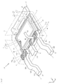
- the semiconductor device A1 of the present embodiment includes a semiconductor element 1, a first lead 2, a second lead 3, a second lead 4, a conductive member 61, a conductive member 62, and a resin portion 8.
- FIG. 1 is a perspective view showing the semiconductor device A1.
- FIG. 2 is a perspective view showing the semiconductor device A1.
- FIG. 3 is a plan view showing the semiconductor device A1.
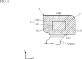
- FIG. 4 is a plan view showing a second pad portion of the semiconductor device A1.
- FIG. 5 is a plan view showing a second pad portion of the semiconductor device A1.
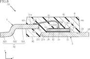
- FIG. 6 is a cross-sectional view taken along the line VI-VI of FIG.
- FIG. 7 is an enlarged cross-sectional view of a main part showing the semiconductor device A1.
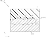
- FIG. 8 is an enlarged cross-sectional view of a main part showing an example of the first roughened region of the semiconductor device A1.
- FIG. 9 is an enlarged cross-sectional view of a main part showing an example of the second roughened region of the semiconductor device A1.
- FIG. 10 is a cross-sectional view taken along the line XX of FIG.
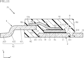
- FIG. 11 is a cross-sectional view taken along the line XI-XI of FIG.
- FIG. 12 is a cross-sectional view taken along the line XII-XII of FIG.
- the z direction corresponds to the first direction of the present disclosure
- the y direction corresponds to the second direction of the present disclosure
- the x direction corresponds to the third direction of the present disclosure.
- the semiconductor element 1 is an electronic component that is a functional center of the semiconductor device A1 and is made of a semiconductor material. Examples of such semiconductor materials include, but are not limited to, Si (silicon), SiC (silicon carbide), and GaAs (gallium arsenide).
- the semiconductor element 1 is, for example, a power semiconductor chip such as a MOSFET (Metal Oxide Semiconductor Field Effect Transistor).
- the semiconductor element 1 is a MOSFET
- the present invention is not limited to this, and other transistors such as an IGBT (Insulated Gate Bipolar Transistor), or a Schottky barrier diode or a first It may be a diode such as a recovery diode.
- IGBT Insulated Gate Bipolar Transistor
- Schottky barrier diode or a first It may be a diode such as a recovery diode.
- the semiconductor element 1 of the present embodiment has an element main surface 1a, an element back surface 1b, a plurality of main surface electrodes 11 and a drain electrode 12.
- the element main surface 1a is a surface facing one side in the z direction (upper side in the drawings in FIGS. 1, 2 and 6).
- the element back surface 1b is a surface facing the other side (lower side in the drawings in FIGS. 1, 2 and 6) opposite to the element main surface 1a in the z direction.
- the plurality of main surface electrodes 11 are formed on the element main surface 1a.
- the plurality of main surface electrodes 11 include a gate electrode 111 and a source electrode 112.
- the gate electrode 111 is an electrode to which a gate voltage is applied to the semiconductor device A1 as a switching element.
- the source electrode 112 is an electrode used as an input / output terminal.
- the gate electrode 111 is smaller than the source electrode 112.
- the gate electrode 111 is unevenly arranged on one side of the element main surface 1a in the x direction (left side in the drawing in FIG. 3).
- the drain electrode 12 is formed on the back surface 1b of the element, and is an electrode used as an input / output terminal together with the source electrode 112.
- the first reed 2 is a member on which the semiconductor element 1 is mounted.
- the first reed 2 is made of a first metal which is a conductive material.
- the first metal in the present embodiment include, but are not limited to, Cu, or may be Ni (nickel), an alloy of Cu or Ni, 42 alloy, or the like.
- the first reed 2 is formed into an appropriate shape from a thin metal plate such as Cu having a rectangular shape in a plan view by punching, cutting, bending, or the like. As shown in FIGS. 1 to 3, 6, 10 and 11, the first reed 2 of the present embodiment has a first pad portion 21, an extending portion 22, a protruding portion 23 and a connecting portion 24.
- the first pad portion 21 has a first pad main surface 21a and a first pad back surface 21b.
- the first pad main surface 21a faces one side in the z direction
- the first pad back surface 21b faces the other side in the z direction.
- the semiconductor element 1 is mounted on the first pad main surface 21a.
- the shape of the first pad portion 21 is not limited in any way, and in the illustrated example, it is substantially rectangular when viewed along the z direction. Further, as shown in FIGS. 6 and 10 to 12, in the present embodiment, the back surface 21b of the first pad is exposed from the resin portion 8.
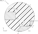
- the first pad main surface 21a has a first smoothing region 211 and a first roughening region 212.
- the hatching composed of a plurality of discrete points indicates a region roughened by the roughening means.
- hatching composed of a plurality of parallel lines indicates a plated region.
- FIG. 7 is an enlarged cross-sectional view of a main part obtained by enlarging a part of FIG.
- the first pad main surface 21a of the illustrated example is a surface that is not plated or is exposed and the first metal such as Cu is exposed.
- the first smoothing region 211 is a region to which the element back surface 1b of the semiconductor element 1 is joined.
- the drain electrode 12 formed on the back surface 1b of the element is conductively bonded to the first smoothing region 211 by the conductive bonding material 19.
- the conductive bonding material 19 extends over substantially the entire area of the first smoothing region 211. It should be noted that there is no limitation on which part of the first smoothing region 211 the conductive bonding material 19 adheres to.
- the first smoothing region 211 includes all of the semiconductor element 1 when viewed along the z direction, and extends from the semiconductor element 1 in all directions.
- the shape of the first smoothing region 211 is not limited in any way, and in the illustrated example, it is substantially rectangular.
- the first roughened region 212 is a region that is separated from the semiconductor element 1 when viewed along the z direction and is coarser than the first smoothed region 211.
- the means for making the first roughened region 212 coarser than the first smoothed region 211 is not limited in any way.
- the first smoothing region 211 is composed of the surface of a metal plate which is a material for a general lead frame, and the first roughening region 212 is a region roughened by a roughening means using a laser. Be done.
- the type of laser used for roughening is not limited in any way, and UV laser, IR laser, Green laser and the like are appropriately exemplified.
- the first roughened region 212 of the illustrated example reaches the edge of the first pad main surface 21a.
- the first roughened region 212 includes a first part 2121, a second part 2122 and a pair of third parts 2123.
- the first portion 2121 is located on one side in the y direction with respect to the first smoothing region 211 (the side on which the second pad portion 31 and the second pad portion 41 described later are located).
- the second part 2122 is located on the opposite side of the first smoothing region 211 from the first part 2121 (and the second pad part 31 and the second pad part 41 described later).
- the pair of third parts 2123 are adjacent to both sides of the first smoothing region 211 in the x direction.
- the first roughened region 212 surrounds the first smoothed region 211 as viewed along the z direction by including the first part 2121, the second part 2122 and the pair of third parts 2123. It has a rectangular ring shape.
- the y-direction dimension of the first part 2121 is smaller than the y-direction dimension of the portion of the first smoothing region 211 located between the first part 2121 and the semiconductor element 1 in the y direction.
- the y-direction dimension of the second part 2122 is smaller than the y-direction dimension of the portion of the first smoothing region 211 located between the second part 2122 and the semiconductor element 1 in the y direction.
- the x-direction dimension of the third part 2123 is smaller than the x-direction dimension of the portion of the first smoothing region 211 located between the third part 2123 and the semiconductor element 1 in the x direction.
- FIG. 8 is a cross-sectional view of a part of the first roughened region 212 which is further enlarged.
- the first roughened region 212 of the illustrated example is roughened using, for example, a Green laser.
- the first roughened region 212 has a plurality of concave portions 212a and a plurality of convex portions 212b.
- the plurality of concave portions 212a and the plurality of convex portions 212b are arranged side by side alternately.
- the first roughened region 212 having the plurality of concave portions 212a and the plurality of convex portions 212b is formed on the first pad main surface 21a by repeating, for example, sequentially scanning the Green laser in a predetermined direction.
- the first roughened region 212 composed of the plurality of recesses 212a and the plurality of convex portions 212b may have a configuration including, for example, a plurality of recesses 212a each having a circular shape or the like.
- the first roughened region 212 of the illustrated example has a plurality of fine protrusions 212c.
- the plurality of fine protrusions 212c are fine protrusions whose respective sizes are clearly smaller than those of the concave portion 212a and the convex portion 212b and are present on the surface of the concave portion 212a or the convex portion 212b. It has been found that when the first roughened region 212 is formed by using a Green laser, a plurality of fine protrusions 212c are present in substantially the entire area of the first roughened region 212, and each shape tends to be a complicated shape. Obtained by the inventor's research.
- the first pad portion 21 of the present embodiment is formed with a locking portion 251.
- the locking portion 251 is a portion having a shape portion protruding in the x direction or the y direction from the peripheral edge portion of the first pad portion 21.
- the locking portion 251 is provided, for example, in order to increase the holding force of the first pad portion 21 by the resin portion 8 by engaging with a part of the resin portion 8.
- the extending portion 22 is one side in the y direction with respect to the first pad portion 21 (the side on which the second pad portion 31 and the second pad portion 41 described later are located). ) Is the part that extends to.
- the shape of the extending portion 22 is not particularly limited, and in the illustrated example, the extending portion 22 has a root portion 221, a bent portion 222, and a tip portion 223.
- the root portion 221 extends from the first pad portion 21 to one side in the y direction and has a shape along the y direction.
- the bent portion 222 is connected to the tip of the root portion 221 in the y direction, and is a shaped portion that is bent to one side in the z direction (upper side in the drawing in FIG. 10) when viewed along the x direction.
- the tip portion 223 is connected to the bent portion 222 and extends from the bent portion 222 to one side in the y direction along the y direction. In the illustrated example, a part of the tip portion 223 protrudes from the resin portion 8.
- the protruding portion 23 is a portion located on the other side in the y direction with respect to the first pad portion 21.
- the shape of the protruding portion 23 is not limited in any way, and in the illustrated example, it is a substantially long rectangular shape with the x direction as the longitudinal direction when viewed along the z direction, and most of them are exposed from the resin portion 8.
- the connecting portion 24 is a portion that connects the first pad portion 21 and the protruding portion 23. As shown in FIG. 3, the connecting portion 24 of the illustrated example has a through hole 241. The through hole 241 penetrates the connecting portion 24 in the z direction.
- the extending portion 22 of the present embodiment has a plating portion 224.
- the plating portion 224 is a metal layer made of a second metal formed by plating on a first metal such as Cu that constitutes the first reed 2.
- the second metal constituting the plated portion 224 is not limited in any way, and is, for example, Ni, Ag, or the like.
- the second lead 3 is a member to which the conductive member 61 described later is joined.
- the second lead 3 is made of a first metal which is a conductive material.
- the first metal in the present embodiment include, but are not limited to, Cu, or may be Ni (nickel), an alloy of Cu or Ni, 42 alloy, or the like.
- the second lead 3 is formed into an appropriate shape from a thin metal plate such as Cu having a rectangular shape in a plan view by punching, cutting, bending, or the like. As shown in FIGS. 1 to 4 and 6, the second lead 3 of the present embodiment has a second pad portion 31 and a terminal portion 32.
- the second pad portion 31 has a second pad main surface 31a and a second pad back surface 31b.
- the second pad main surface 31a faces one side in the z direction
- the second pad back surface 31b faces the other side in the z direction.
- a conductive member 61 which will be described later, is joined to the second pad main surface 31a.
- the shape of the second pad portion 31 is not limited in any way, and in the illustrated example, it is substantially rectangular when viewed along the z direction. Further, as shown in FIG. 6, in the present embodiment, the second pad main surface 31a and the second pad back surface 31b are covered with the resin portion 8.
- the second pad portion 31 is located on one side in the y direction with respect to the first pad portion 21 when viewed along the z direction. It is located on one side of the extension portion 22 in the x direction. Further, the second pad portion 31 is located on one side in the z direction (upper side in the drawing in FIG. 6) with respect to the first pad portion 21 and the extending portion 22.
- the second pad main surface 31a has a second smoothing region 311 and a second roughening region 312.
- FIG. 7 is an enlarged cross-sectional view of a main part obtained by enlarging a part of FIG.
- the second pad main surface 31a of the illustrated example is plated.
- the second metal constituting the metal layer formed by plating is not limited in any way, and examples thereof include Ni and Ag.
- the second smoothing region 311 is a region to which the second bonding portion 612, which will be described later, of the conductive member 61 is bonded.
- the second smoothing region 311 includes all of the second bonding portion 612 when viewed along the z direction, and extends in all directions from the semiconductor element 1.
- the shape of the second smoothing region 311 is not limited in any way, and in the illustrated example, it is substantially rectangular.
- the second smoothed region 311 of the illustrated example is a plated smoothed region.
- the x-direction dimension of the second smoothing region 311 is preferably twice or more the x-direction dimension of the second bonding portion 612.
- the second roughened region 312 is a region that is separated from the second bonding portion 612 when viewed along the z direction and is coarser than the second smoothed region 311.
- the means for making the second roughened region 312 coarser than the second smoothed region 311 is not limited in any way.
- the second smoothing region 311 is composed of the surface of a metal plate which is a material for a general lead frame, and the second roughening region 312 is a region roughened by a roughening means using a laser. Be done.
- the type of laser used for roughening is not limited in any way, and UV laser, IR laser, Green laser and the like are appropriately exemplified.
- the second roughened region 312 reaches the edge of the second pad main surface 31a.
- the second roughened region 312 includes a first part 3121, a second part 3122 and a pair of third parts 3123.
- the first portion 3121 is located on the other side (the side where the first pad portion 21 is located) in the y direction with respect to the second smoothing region 311.
- the second part 3122 is located on the side opposite to the first part 3121 (and the first pad part 21) with respect to the second smoothing region 311.
- the pair of third parts 3123 are adjacent to both sides of the second smoothing region 311 in the x direction.
- the second roughened region 312 surrounds the second smoothed region 311 as viewed along the z direction by including a first part 3121, a second part 3122 and a pair of third parts 3123. It has a rectangular ring shape.
- FIG. 9 is a cross-sectional view of a part of the second roughened region 312 which is further enlarged.
- the second roughened region 312 of the illustrated example is roughened using, for example, a Green laser.
- the second roughened region 312 has a plurality of recesses 312a and a plurality of protrusions 312b.
- the plurality of concave portions 312a and the plurality of convex portions 312b are arranged side by side alternately.
- the second roughened region 312 having the plurality of concave portions 312a and the plurality of convex portions 312b is formed on the second pad main surface 31a by repeating, for example, sequentially scanning the Green laser in a predetermined direction. It is a structure in which a groove is formed.
- the second roughened region 312 composed of the plurality of concave portions 312a and the plurality of convex portions 312b may have a configuration including, for example, a plurality of concave portions 312a each having a circular shape or the like.
- the plurality of recesses 312a are regions where Cu, which is the first metal of the second lead 3, is exposed.
- the plurality of convex portions 312b are second metals forming the metal layer 319 formed by plating, and are made of, for example, Ni.
- Such a second roughened region 312 has a configuration that can be seen when the first metal is covered with the metal layer 319 by plating and then the second roughened region 312 is formed by a roughening means such as a Green laser. be.
- the thickness of the metal layer 319 is 2 ⁇ m to 4 ⁇ m, and the uneven dimension of the second roughened region 312 (the dimension from the bottom of the concave portion 312a to the top of the convex portion 312b) is larger than the thickness of the metal layer 319. For example, it is 5 ⁇ m to 8 ⁇ m.
- the second roughened region 312 of the illustrated example has a plurality of fine protrusions 312c.
- Each of the plurality of fine protrusions 312c is clearly smaller in size than the concave portion 312a and the convex portion 312b, and is a finer protrusion existing on the surface of the concave portion 312a and the convex portion 312b. It has been found that when the second roughened region 312 is formed by using the Green laser, a plurality of fine protrusions 312c are present in substantially the entire area of the second roughened region 312, and each shape tends to be a complicated shape. Obtained by the inventor's research.
- the terminal portion 32 is a portion extending to one side in the y direction with respect to the second pad portion 31.
- the terminal portion 32 is used, for example, when mounting the semiconductor device A1 on a circuit board or the like.
- the shape of the terminal portion 32 is not particularly limited, and in the illustrated example, the terminal portion 32 has a root portion 321, a bent portion 322, and a tip portion 323.
- the root portion 321 extends from the second pad portion 31 to one side in the y direction and has a shape along the y direction. A part of the root portion 321 is exposed from the resin portion 8.
- the bent portion 322 is a shape portion connected to the tip of the root portion 321 in the y direction and bent to the other side in the z direction (lower side in the drawing in FIG. 6) when viewed along the x direction.
- the tip portion 323 is connected to the bent portion 322 and extends from the bent portion 322 to one side in the y direction along the y direction.
- the second lead 4 is a member to which the conductive member 62 described later is joined.
- the second reed 4 is made of a first metal which is a conductive material.
- the first metal in the present embodiment include, but are not limited to, Cu, or may be Ni (nickel), an alloy of Cu or Ni, 42 alloy, or the like.
- the second reed 4 is formed into an appropriate shape from a thin metal plate such as Cu having a rectangular shape in a plan view by punching, cutting, bending, or the like. As shown in FIGS. 1 to 3, 5 and 11, the second lead 4 of the present embodiment has a second pad portion 41 and a terminal portion 42.
- the second pad portion 41 has a second pad main surface 41a and a second pad back surface 41b.
- the second pad main surface 41a faces one side in the z direction
- the second pad back surface 41b faces the other side in the z direction.
- a conductive member 62 which will be described later, is joined to the second pad main surface 41a.
- the shape of the second pad portion 41 is not limited in any way, and in the illustrated example, it is substantially rectangular when viewed along the z direction. Further, as shown in FIG. 6, in the present embodiment, the second pad main surface 41a and the second pad back surface 41b are covered with the resin portion 8.
- the second pad portion 41 is located on one side in the y direction with respect to the first pad portion 21 when viewed along the z direction. It is located on the other side of the extension portion 22 in the x direction. Further, the second pad portion 41 is located on one side in the z direction (upper side in the drawing in FIG. 10) with respect to the first pad portion 21 and the extension portion 22, and the positions of the second pad portion 31 and the z direction are located. It is almost the same.
- the second pad main surface 41a has a second smoothing region 411 and a second roughening region 412.
- the second pad main surface 41a of the illustrated example is plated.
- the second metal constituting the metal layer formed by plating is not limited in any way, and examples thereof include Ni and Ag.
- the second smoothing region 411 is a region to which the second bonding portion 622 described later of the conductive member 62 is bonded.
- the second smoothing region 411 includes all of the second bonding portion 622 when viewed along the z direction, and extends in all directions from the semiconductor element 1.
- the shape of the second smoothing region 411 is not limited in any way, and in the illustrated example, it is substantially rectangular.
- the second smoothed region 411 of the illustrated example is a plated smoothed region.
- the x-direction dimension of the second smoothing region 411 is preferably twice or more the x-direction dimension of the second bonding portion 622.
- the second roughened region 412 is a region that is separated from the second bonding portion 622 and is coarser than the second smoothed region 411 when viewed along the z direction.
- the means for making the second roughened region 412 coarser than the second smoothed region 411 is not limited in any way.
- the second smoothed region 411 is composed of the surface of a metal plate which is a material for a general lead frame, and the second roughened region 412 is roughened by a laser roughening means.
- a configuration that is a roughened region can be mentioned.
- the type of laser used for roughening is not limited in any way, and UV laser, IR laser, Green laser and the like are appropriately exemplified.
- the second roughened region 412 reaches the edge of the second pad main surface 41a.
- the second roughened region 412 includes a first part 4121, a second part 4122 and a pair of third parts 4123.
- the first portion 4121 is located on the other side (the side where the first pad portion 21 is located) in the y direction with respect to the second smoothing region 411.
- the second part 4122 is located on the side opposite to the first part 4121 (and the first pad part 21) with respect to the second smoothing region 411.
- the pair of third parts 4123 are adjacent to both sides of the second smoothing region 411 in the x direction.
- the second roughened region 412 surrounds the second smoothed region 411 when viewed along the z direction by including a first part 4121, a second part 4122 and a pair of third parts 4123. It has a rectangular ring shape.
- the specific detailed configuration of the second roughened region 412 is not limited in any way, and is, for example, the same configuration as the second roughened region 412 shown in FIG.
- the terminal portion 42 is a portion extending to one side in the y direction with respect to the second pad portion 41.
- the terminal portion 42 is used, for example, when mounting the semiconductor device A1 on a circuit board or the like.
- the shape of the terminal portion 42 is not particularly limited, and in the illustrated example, the terminal portion 42 has a root portion 421, a bent portion 422, and a tip portion 423.
- the root portion 421 extends from the second pad portion 41 to one side in the y direction and has a shape along the y direction. A part of the root portion 421 is exposed from the resin portion 8.
- the bent portion 422 is connected to the tip of the root portion 421 in the y direction, and is a shaped portion that is bent toward the other side in the z direction (lower side in the drawing in FIG. 6) when viewed along the x direction.
- the tip portion 423 is connected to the bent portion 422 and extends from the bent portion 422 to one side in the y direction along the y direction.
- the roughness of the first roughened region 212 of the first pad portion 21, the second roughened region 312 of the second pad portion 31, and the second roughened region 412 of the second pad portion 41 is not limited in any way.
- the arithmetic average roughness Sa of the surface roughness is 0.34 to 4.2.
- the maximum height Sz is 3.6 to 26
- the line roughness is Ra of 0.33 to 3.9
- the maximum height Rz is 1.7 to 13.
- the arithmetic mean song Spc of the peak peak is 1400 to 5700.
- the development area ratio Sdr of the interface is 0.067 to 2.2.
- the roughness of the first roughened region 212 is the second roughened. Rougher than the roughness of the region 312 or the second roughened region 412.
- the number of times the same portion is scanned by the laser in the roughening process for forming the first roughened region 212 is determined by the second roughened region 312 and the second roughened region.
- the roughening process for forming the chemical region 412 there is a method in which the same portion is scanned more than the number of times by the laser.
- the same portion is scanned once by the laser, and in the formation of the first roughened region 212, the same portion is scanned twice or more by the laser. Scan multiple times.
- the recess 212a of the first roughening region 212 shown in FIG. 8 may have a multi-stage shape corresponding to the number of scans.
- the conduction member 61 is for conducting the gate electrode 111 of the semiconductor element 1 and the second lead 3.
- the specific configuration of the conductive member 61 is not limited in any way, and examples thereof include wires and ribbons made of metal.
- Examples of the metal constituting the conductive member 61 include metals such as Au and Al and alloys thereof.
- Examples of the Al alloy include an Al alloy in which any of Fe, Si, and Ni is added to Al.
- the conductive member 61 is a wire made of Au.
- the conductive member 61 has a first bonding portion 611 and a second bonding portion 612.
- the first bonding portion 611 is bonded to the gate electrode 111 of the semiconductor element 1.
- the second bonding portion 612 is bonded to the second smoothing region 311 of the second pad main surface 31a of the second pad portion 31 of the second lead 3.
- the forming order of the first bonding portion 611 and the second bonding portion 612 is not limited at all.
- the conductive member 61 is formed by, for example, capillary bonding.
- the conduction member 61 is for conducting the source electrode 112 of the semiconductor element 1 and the second lead 4.
- the specific configuration of the conductive member 62 is not limited in any way, and examples thereof include wires and ribbons made of metal.
- Examples of the metal constituting the conductive member 61 include metals such as Au and Al and alloys thereof.
- Examples of the Al alloy include an Al alloy in which any of Fe, Si, and Ni is added to Al.
- the conductive member 62 is a wire made of Al or an Al alloy. In this case, the diameter of the conductive member 62 is larger than the diameter of the conductive member 61.
- the conductive member 62 has a first bonding portion 621 and a second bonding portion 622.
- the first bonding portion 621 is bonded to the source electrode 112 of the semiconductor element 1.
- the second bonding portion 622 is bonded to the second smoothing region 411 of the second pad main surface 41a of the second pad portion 41 of the second lead 4.
- the forming order of the first bonding portion 621 and the second bonding portion 622 is not limited at all.
- the conductive member 62 is formed, for example, by wedge bonding.
- the resin portion 8 covers the conductive member 61 and the conductive member 62, respectively, with a part of each of the semiconductor element 1, the first lead 2, the second lead 3, and the second lead 4.
- the resin portion 8 is a thermosetting synthetic resin having electrical insulation.
- the resin portion 8 is a black epoxy resin, and a filler may be appropriately mixed therein.
- the resin portion 8 has a resin main surface 81, a resin back surface 82, a resin end surface 83, a resin end surface 84, and a pair of resin side surfaces 85. There is.
- the resin main surface 81 and the resin back surface 82 face each other and are separated from each other in the z direction.
- the resin main surface 81 faces the same direction as the element main surface 1a
- the resin back surface 82 faces the same direction as the element back surface 1b.
- Each of the resin end surface 83, the resin end surface 84, and the pair of resin side surfaces 85 is sandwiched between the resin main surface 81 and the resin back surface 82.
- the resin end face 83 faces one side in the y direction.
- the resin end face 84 faces the other side in the y direction.
- the pair of resin side surfaces 85 face both sides in the y direction.
- the back surface 21b of the first pad is exposed from the back surface 82 of the resin. Further, the extending portion 22, the terminal portion 32, and the terminal portion 42 project from the resin end surface 83. Further, the protruding portion 23 protrudes from the resin end surface 84.
- a first roughened region 212 is formed in the first pad portion 21, and a second roughened region is formed in the second pad portion 31. 312 is formed.
- the first pad portion 21, the second pad portion 31, and the resin portion 8 are separated from each other by establishing a local engagement relationship between the first roughened region 212, the second roughened region 312, and the resin portion 8. Etc. can be suppressed.
- the semiconductor element 1 is mounted on the first smoothing region 211. As a result, it is possible to avoid a decrease in the bonding strength between the semiconductor element 1 and the first pad portion 21. Further, the second bonding portion 612 of the conductive member 61 is joined to the second smoothing region 311.
- the second bonding portion 612 is bonded to a smoother portion in order to improve the bonding strength. Further, since the second smoothing region 411 and the second roughening region 412 are provided in the second pad portion 41, the same effect can be expected. Therefore, it is possible to improve the adhesion between the resin portion 8 and the first reed 2, the second reed 3, and the second reed 4 while achieving appropriate operation of the semiconductor device A1. Further, since the second smoothing region 411 and the second roughening region 412 are provided in the second pad portion 41, the same effect can be expected.
- the first roughened region 212 includes the first part 2121. As a result, it is possible to prevent the first pad portion 21 and the resin portion 8 from being peeled off from the side on which the second pad portion 31 and the second pad portion 41 are arranged.
- the first roughened region 212 includes the second part 2122. As a result, it is possible to prevent the first pad portion 21 and the resin portion 8 from being peeled off from the side opposite to the side on which the second pad portion 31 and the second pad portion 41 are arranged, that is, the side of the protruding portion 23. can do. Further, the first roughened region 212 includes the third part 2123.
- the configuration in which the first roughened region 212 reaches the edge of the first pad main surface 21a is preferable in order to avoid peeling between the first pad portion 21 and the resin portion 8.
- the second roughened region 312 includes the first part 3121. As a result, it is possible to prevent the second pad portion 31 and the resin portion 8 from being peeled off from the side on which the first pad portion 21 is arranged.
- the second roughened region 312 includes the second part 3122. As a result, it is possible to prevent the second pad portion 31 and the resin portion 8 from being peeled off from the side opposite to the side on which the first pad portion 21 is arranged, that is, the side of the terminal portion 32.
- the second roughened region 312 includes the third part 3123. As a result, it is possible to prevent the second pad portion 31 and the resin portion 8 from being peeled off from the outside in the x direction. Further, the configuration in which the second roughened region 312 reaches the edge of the second pad main surface 31a is preferable in order to avoid peeling between the second pad portion 31 and the resin portion 8.
- the second roughened region 412 includes the first part 4121. As a result, it is possible to prevent the second pad portion 41 and the resin portion 8 from being peeled off from the side on which the first pad portion 21 is arranged.
- the second roughened region 412 includes the second part 4122. As a result, it is possible to prevent the second pad portion 41 and the resin portion 8 from being peeled off from the side opposite to the side on which the first pad portion 21 is arranged, that is, the side of the terminal portion 42.
- the second roughened region 412 includes the third part 4123. As a result, it is possible to prevent the second pad portion 41 and the resin portion 8 from being peeled off from the outside in the x direction. Further, the configuration in which the second roughened region 412 reaches the edge of the second pad main surface 41a is preferable in order to avoid peeling between the second pad portion 41 and the resin portion 8.
- the first smoothing region 211 is a smooth surface that is not plated or is exposed and, for example, Cu, which is the first metal, is exposed. This is preferable for joining the semiconductor element 1 with the conductive bonding material 19.
- a second metal such as Ni is provided by plating in the second smoothing region 311 and the second smoothing region 411. As a result, the bonding strength of the second bonding portion 612 and the second bonding portion 622 can be increased.
- the first roughened region 212 has a plurality of fine protrusions 212c.
- the effect of preventing peeling between the first pad portion 21 and the resin portion 8 can be further enhanced.
- a plurality of fine protrusions 212c are likely to occur.
- the second roughened region 312 has a plurality of fine protrusions 312c.
- the effect of preventing peeling between the second pad portion 31 and the resin portion 8 can be further enhanced.
- a plurality of second roughened regions 312c are likely to occur.
- a roughening treatment using a laser such as a Green laser is performed.
- the concave portion 312a made of the first metal and the convex portion 312b made of the second metal are formed, and appropriate roughening can be performed.
- the plurality of recesses 312a are regions where Cu, which is the first metal of the second lead 3, is exposed.
- the plurality of convex portions 312b are second metals forming the metal layer 319 formed by plating, and are made of, for example, Ni. As described above, in the case where the recess 312a penetrates the metal layer 319 and reaches the first metal, the effect of significantly suppressing the peeling of the resin portion 8 has been confirmed by the inventor's test.
- the roughness of the first roughened region 212 coarser than that of the second roughened region 312 and the second roughened region 412, peeling between the first pad portion 21 and the resin portion 8 can be more reliably suppressed. ..
- the semiconductor element 1 is a power semiconductor chip, a larger temperature change may occur in the first pad portion 21. It is preferable to prevent peeling more reliably in such a portion.
- FIG. 13 is a cross-sectional view of a part of the second roughened region 312 of the first modification of the semiconductor device A1 which is further enlarged.
- the second roughened region 312 of the semiconductor device A11 of this modification is roughened using, for example, a Green laser, similarly to the second roughened region 312 of the semiconductor device A1.
- the plurality of recesses 312a remain in the metal layer 319. That is, in the recess 312a, Cu, which is the first metal of the second lead 3, is not exposed.
- the thickness of the metal layer 319 is 3 ⁇ m to 6 ⁇ m, and the uneven dimension of the second roughened region 312 (the dimension from the bottom of the concave portion 312a to the top of the convex portion 312b) is smaller than the thickness of the metal layer 319. For example, it is 1 ⁇ m to 4 ⁇ m.
- the second roughened region 312 has a plurality of fine protrusions 312c.
- the second roughened region 312 is not limited to the case where the first metal of the second lead 3 is exposed in the recess 312a, and the first metal may not be exposed. .. Even with such a configuration, the adhesion to the resin portion 8 can be promoted by having the concave portion 312a and the convex portion 312b and having the fine protrusion 312c.
- FIG. 14 shows a second modification of the semiconductor device A1.
- the semiconductor device A12 of this example further includes a semiconductor element 1A and a conductive member 63.
- the semiconductor element 1A is, for example, a diode.
- the first pad main surface 21a of the first pad portion 21 has two first smoothing regions 211.
- the semiconductor element 1 is mounted in one first smoothing region 211, and the semiconductor element 1A is mounted in the other first smoothing region 211.
- the first roughened region 212 of this modification has a fourth part 2124 in addition to the first part 2121, the second part 2122, and the pair of the third part 2123.
- the fourth part 2124 has a shape extending in the y direction, and is connected to the first part 2121 and the second part 2122.
- Part 4 2124 partitions the two first smoothed regions 211 from each other.
- the conductive member 63 has a first bonding portion 631 and a second bonding portion 632.
- the material of the conductive member 63 is not particularly limited, and is made of, for example, Au, Al, or an alloy thereof.
- the first bonding portion 631 is bonded to the main surface electrode 11A of the semiconductor element 1A.
- the second bonding portion 632 is bonded to the second smoothing region 411 of the second pad main surface 41a of the second lead 4. That is, in this example, the second bonding portion 622 and the second bonding portion 632 are bonded to one second roughened region 412.
- the semiconductor device of the present disclosure may be configured to include a plurality of semiconductor elements of two or three or more. Further, the second coarsening region of the present disclosure may be configured such that two or three or more conductive members are joined.
- FIG. 15 shows a third modification of the semiconductor device A1.
- the configuration of the semiconductor element 1 is different from the above-mentioned example.
- the semiconductor device A1 of this modification is, for example, a diode.
- the first bonding portion 611 and the first bonding portion 621 are both bonded to the main surface electrode 11.
- Both the conductive member 61 and the conductive member 62 are made of, for example, Al or an Al alloy.
- the second bonding portion 612 is bonded to the second smoothed region 311 and the second bonding portion 622 is bonded to the second smoothed region 411.
- the second lead 3 and the second lead 4 are electrically conducting members having the same potential.
- the types of semiconductor elements of the present disclosure are not limited in any way. Further, the conductive member and the second lead of the present disclosure are appropriately set according to the configuration of the semiconductor element and the like.
- the semiconductor device A2 of the present embodiment includes a semiconductor element 1, a first lead 2, a second lead 3, a second lead 4, a conductive member 61, a plurality of conductive members 62, and a resin portion 8.
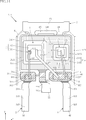
- FIG. 16 is a perspective view showing the semiconductor device A2.
- FIG. 17 is a plan view showing the semiconductor device A2.
- FIG. 18 is a cross-sectional view taken along the line XVII-XVII of FIG.
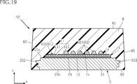
- FIG. 19 is a cross-sectional view taken along the line XVIII-XVIII of FIG.
- FIG. 20 is a cross-sectional view taken along the line XIX-XIX of FIG.
- the semiconductor element 1 has, for example, the same configuration as the semiconductor element 1 of the semiconductor device A1, and has a plurality of main surface electrodes 11 including a gate electrode 111 and a source electrode 112, and a drain electrode 12.
- the first reed 2 has a first pad portion 21.
- the configuration of the first pad portion 21 is similar to that of the first pad portion 21 of the semiconductor device A1.
- the first pad portion 21 of the present embodiment is formed with a locking portion 252, a locking portion 253, and a locking portion 254.
- the locking portion 252, the locking portion 253, and the locking portion 254 are for improving the holding force of the first pad portion 21 by the resin portion 8 in the same manner as the locking portion 251.
- the locking portion 252 and the locking portion 253 are formed side by side in the y direction.
- the locking portion 254 is provided so as to project from the first pad portion 21 to the side where the second lead 3 and the second lead 4 are located in the y direction.
- the shape of the second pad portion 31 of the second lead 3 is different from that of the second pad portion 31 in the semiconductor device A1. Further, the second smoothing region 311 of the present embodiment has a shape elongated in a direction inclined with respect to the y direction.
- the first bonding portion 611 of the conductive member 61 is bonded to the gate electrode 111 of the semiconductor element 1.
- the second bonding portion 612 is bonded to the second smoothing region 311.
- the second bonding portion 612 is joined to the second smoothing region 311 so that the longitudinal direction of the second bonding portion 612 and the longitudinal direction of the second smoothing region 311 substantially coincide with each other.
- the conductive member 61 is, for example, a wire made of Au.
- the second lead 4 of the present embodiment has a second pad portion 41, a plurality of terminal portions 42, and an extension portion 43.
- the second pad portion 41 of the present embodiment has a shape that extends long in the x direction when viewed along the z direction.
- the second pad main surface 41a of the present embodiment has a plurality of second smoothing regions 411 and a second roughening region 412.
- the plurality of second smoothing regions 411 have an elongated rectangular shape with the y direction as the longitudinal direction, and are arranged apart from each other in the x direction.
- a part of the second roughened region 412 is arranged between the adjacent second smoothed regions 411.
- the plurality of terminal portions 42 extend from the second pad portion 41 in the y direction and are arranged apart from each other in the x direction.
- the extending portion 43 extends from the second pad portion 41 in the x direction, and is arranged between the two terminal portions 42 in the x direction.
- Each of the first bonding portions 621 of the plurality of conductive members 62 is bonded to the source electrode 112 of the semiconductor element 1.
- the second bonding portions 622 of the plurality of conductive members 62 are individually bonded to the plurality of second smoothing regions 411.
- the longitudinal direction of the second bonding portion 622 and the longitudinal direction of the second smoothing region 411 substantially coincide with each other and are along the substantially y direction.
- the resin portion 8 of this embodiment has two recesses 851.
- the recess 851 is a portion recessed from the resin main surface 81 and the pair of resin side surfaces 85.
- a plurality of conductive members 62 may be joined to one source electrode 112 (main surface electrode 11). Further, the second bonding portions 622 of the plurality of conductive members 62 may be individually bonded to the plurality of second smoothing regions 411 provided in one second pad portion 41.
- FIG. 21 shows a first modification of the semiconductor device A2.
- the semiconductor device A21 of the present embodiment includes a semiconductor element 1, a first lead 2, a second lead 3, a second lead 4, a second lead 5, a conductive member 61, a plurality of conductive members 62, a conductive member 63, and a resin portion 8. To be equipped.
- the plurality of main surface electrodes 11 of the semiconductor element 1 include a gate electrode 111, a source electrode 112, and a source sense electrode 113.
- the source sense electrode 113 has the same shape and size as the gate electrode 111, for example, and is arranged side by side in the x direction together with the gate electrode 111.
- the second lead 4 is arranged so as to be separated from the second lead 3 in the x direction, and has a second pad portion 41, a plurality of terminal portions 42, and an extension portion 43.
- the second lead 5 has a configuration similar to that of the second lead 3 (and the second lead 4). In the present embodiment, the second lead 5 is arranged between the second lead 3 and the second lead 4 in the x direction.
- the second lead 5 has a second pad portion 51 and a terminal portion 52.
- the configuration of the second pad portion 51 and the terminal portion 52 is similar to that of the second pad portion 41 and the terminal portion 42.
- the second pad portion 51 is provided with a second smoothing region 511 and a second roughening region 512.
- the configuration of the second smoothed region 511 and the second roughened region 512 is similar to, for example, the second smoothed region 411 and the second roughened region 412.
- the first bonding portion 611 is bonded to the gate electrode 111, and the second bonding portion 612 is bonded to the second smoothing region 311.
- the first bonding portion 621 is bonded to the source electrode 112, and the second bonding portion 622 is individually bonded to the second smoothing region 411 of the Fuchs.
- the conductive member 63 has a first bonding portion 631 and a second bonding portion 632.
- the configuration of the conductive member 63 is similar to, for example, the conductive member 61.
- the first bonding portion 611 is bonded to the source sense electrode 113, and the second bonding portion 632 is bonded to the second smoothing region 511.
- the configuration of the plurality of main surface electrodes 11 is not limited at all. Further, depending on the configuration of the plurality of main surface electrodes 11, another second lead such as the second lead 5 may be further provided in addition to the second lead 3 and the second lead 4.
- the semiconductor device according to the present disclosure is not limited to the above-described embodiment.
- the specific configuration of each part of the semiconductor device according to the present disclosure can be freely redesigned.
- a semiconductor device having an element main surface and an element back surface facing opposite sides in the first direction, A first lead having a first pad portion on which the semiconductor element is mounted, and a first lead, A second lead having a second pad portion arranged side by side with the first pad portion in a second direction perpendicular to the first direction, and a second lead.
- a conductive member having a first bonding portion bonded to the semiconductor element and a second bonding portion bonded to the second pad portion, It includes the semiconductor element, the conduction member, the first pad portion, and the resin portion that covers the second pad portion.
- the first pad portion is a first coarse region to which the back surface of the element is joined and a region that is separated from the semiconductor element and is coarser than the first smooth region when viewed along the first direction. It has a first pad main surface including a chemical region,
- the second pad portion is a second smoothing region to which the second bonding portion is joined and a region that is separated from the second smoothing portion and is coarser than the second smoothing region when viewed along the first direction.
- the semiconductor device according to any one of Supplementary note 1 to 15, wherein the second lead has a terminal portion protruding from the resin portion in the second direction.
- the semiconductor element has a gate electrode and a source electrode arranged on the main surface of the element, and a drain electrode arranged on the back surface of the element.
- the first bonding portion of the conductive member is bonded to at least one of the gate electrode and the source electrode.
- the semiconductor device according to any one of Supplementary note 1 to 16, wherein the drain electrode is conduction-bonded to the first smoothing region.
Landscapes
- Lead Frames For Integrated Circuits (AREA)
- Wire Bonding (AREA)
- Structures Or Materials For Encapsulating Or Coating Semiconductor Devices Or Solid State Devices (AREA)
Abstract
Description
図1~図12は、本開示の第1実施形態に係る半導体装置を示している。本実施形態の半導体装置A1は、半導体素子1、第1リード2、第2リード3、第2リード4、導通部材61、導通部材62および樹脂部8を備えている。
半導体素子1は、半導体装置A1の機能中枢となる電子部品であり、半導体材料からな。このような半導体材料としては、Si(シリコン)、SiC(炭化ケイ素)およびGaAs(ヒ化ガリウム)などがあるが、これらに限定されない。半導体素子1は、たとえば、MOSFET(Metal Oxide Semiconductor Field Effect Transistor)などのパワー半導体チップである。本実施形態においては、半導体素子1がMOSFETである場合を示すが、これに限定されず、IGBT(Insulated Gate Bipolar Transistor;絶縁ゲートバイポーラトランジスタ)などの他のトランジスタ、あるいは、ショットキーバリアダイオードやファーストリカバリダイオードなどのダイオードであってもよい。
第1リード2は、半導体素子1が搭載される部材である。第1リード2は、導電性材料である第1金属よりなる。本実施形態における第1金属としては、たとえばCuが挙げられるが、これに限定されず、Ni(ニッケル)、または、CuやNiの合金、42アロイなどであってもよい。第1リード2は、平面視矩形状のCuなどの薄肉金属板から、打ち抜き加工、切り取り加工、曲げ加工などにより適切な形に形成される。図1~図3、図6、図10および図11に示すように、本実施形態の第1リード2は、第1パッド部21、延出部22、突出部23および連結部24を有する。
第2リード3は、後述の導通部材61が接合される部材である。第2リード3は、導電性材料である第1金属よりなる。本実施形態における第1金属としては、たとえばCuが挙げられるが、これに限定されず、Ni(ニッケル)、または、CuやNiの合金、42アロイなどであってもよい。第2リード3は、平面視矩形状のCuなどの薄肉金属板から、打ち抜き加工、切り取り加工、曲げ加工などにより適切な形に形成される。図1~図4、および図6に示すように、本実施形態の第2リード3は、第2パッド部31および端子部32を有する。
第2リード4は、後述の導通部材62が接合される部材である。第2リード4は、導電性材料である第1金属よりなる。本実施形態における第1金属としては、たとえばCuが挙げられるが、これに限定されず、Ni(ニッケル)、または、CuやNiの合金、42アロイなどであってもよい。第2リード4は、平面視矩形状のCuなどの薄肉金属板から、打ち抜き加工、切り取り加工、曲げ加工などにより適切な形に形成される。図1~図3、図5および図11に示すように、本実施形態の第2リード4は、第2パッド部41および端子部42を有する。
導通部材61は、半導体素子1のゲート電極111と第2リード3とを導通させるためのものである。導通部材61の具体的構成は何ら限定されず、たとえば金属からなるワイヤやリボンが挙げられる。導通部材61を構成する金属としては、たとえばAu、Al等の金属やこれらの合金が挙げられる。Al合金としては、たとえばAlにFe、Si、Niのいずれかが添加されたAl合金が挙げられる。本実施形態においては、導通部材61は、Auからなるワイヤである。
導通部材61は、半導体素子1のソース電極112と第2リード4とを導通させるためのものである。導通部材62の具体的構成は何ら限定されず、たとえば金属からなるワイヤやリボンが挙げられる。導通部材61を構成する金属としては、たとえばAu、Al等の金属やこれらの合金が挙げられる。Al合金としては、たとえばAlにFe、Si、Niのいずれかが添加されたAl合金が挙げられる。本実施形態においては、導通部材62は、AlまたはAl合金からなるワイヤである。この場合、導通部材62の直径は、導通部材61の直径よりも大きい。
樹脂部8は、半導体素子1、第1リード2、第2リード3および第2リード4の一部ずつ、導通部材61および導通部材62を覆っている。樹脂部8は、電気絶縁性を有する熱硬化性の合成樹脂である。本実施形態においては、樹脂部8は、黒色のエポキシ樹脂であり、適宜フィラーが混入していてもよい。樹脂部8は、図1~図3、図6、図10および図11に示すように、樹脂主面81、樹脂裏面82、樹脂端面83、樹脂端面84および一対の樹脂側面85を有している。
図13は、半導体装置A1の第1変形例の第2粗化領域312の一部をさらに拡大した断面図である。本変形例の半導体装置A11の第2粗化領域312は、半導体装置A1の第2粗化領域312と同様に、たとえばGreenレーザを用いて粗化されたものである。本変形例においては、複数の凹部312aは、金属層319内にとどまっている。すなわち、凹部312aにおいては、第2リード3の第1金属であるCuは露出していない。たとえば、金属層319の厚さが、3μm~6μmであり、第2粗化領域312の凹凸寸法(凹部312aの底部から凸部312bの頂部までの寸法)が、金属層319の厚さよりも小さく、たとえば、1μm~4μmである。
図14は、半導体装置A1の第2変形例を示している。本例の半導体装置A12は、半導体素子1Aおよび導通部材63をさらに備えている。
図15は、半導体装置A1の第3変形例を示している。本変形例の半導体装置A13は、半導体素子1の構成が上述の例と異なっている。本変形例の半導体装置A1は、たとえばダイオードである。
図16~図20は、本開示の第2実施形態に係る半導体装置を示している。本実施形態の半導体装置A2は、半導体素子1、第1リード2、第2リード3、第2リード4、導通部材61、複数の導通部材62および樹脂部8を備えている。
図21は、半導体装置A2の第1変形例を示している。本実施形態の半導体装置A21は、半導体素子1、第1リード2、第2リード3、第2リード4、第2リード5、導通部材61、複数の導通部材62、導通部材63および樹脂部8を備える。
第1方向において互いに反対側を向く素子主面および素子裏面を有する半導体素子と、
前記半導体素子が搭載された第1パッド部を有する第1リードと、
前記第1方向と直角である第2方向において前記第1パッド部と並んで配置された第2パッド部を有する第2リードと、
前記半導体素子に接合された第1ボンディング部および前記第2パッド部に接合された第2ボンディング部を有する導通部材と、
前記半導体素子、前記導通部材、前記第1パッド部および前記第2パッド部を覆う樹脂部と、を備えており、
前記第1パッド部は、前記素子裏面が接合された第1平滑領域および前記第1方向に沿って視て前記半導体素子から離れており且つ前記第1平滑領域よりも粗い領域である第1粗化領域を含む第1パッド主面を有し、
前記第2パッド部は、前記第2ボンディング部が接合された第2平滑領域および前記第1方向に沿って視て前記第2ボンディング部から離れており且つ前記第2平滑領域よりも粗い領域である第2粗化領域を含む第2パッド主面を有する、半導体装置。
〔付記2〕
前記第1粗化領域は、前記第1平滑領域に対して前記第2パッド部側に位置する第1部を含む、付記1に記載の半導体装置。
〔付記3〕
前記第1粗化領域は、前記第1平滑領域に対して前記第2パッド部とは反対側に位置する第2部を含む、付記1または2に記載の半導体装置。
〔付記4〕
前記第1粗化領域は、前記第1方向および前記第2方向と直角である第3方向において前記第1平滑領域に隣接する第3部を含む、付記1ないし3のいずれかに記載の半導体装置。
〔付記5〕
前記第2粗化領域は、前記第2平滑領域に対して前記第1パッド部側に位置する第1部を含む、付記1ないし4のいずれかに記載の半導体装置。
〔付記6〕
前記第2粗化領域は、前記第2平滑領域に対して前記第1パッド部とは反対側に位置する第2部を含む、付記1ないし5のいずれかに記載の半導体装置。
〔付記7〕
前記第2粗化領域は、前記第1方向および前記第2方向と直角である第3方向において前記第2平滑領域に隣接する第3部を含む、付記1ないし6のいずれかに記載の半導体装置。
〔付記8〕
前記第1パッド部は、第1金属を含み、
前記第1パッド主面は、前記第1金属からなる、付記1ないし7のいずれかに記載の半導体装置。
〔付記9〕
前記第2パッド部は、第2金属と、前記第2金属の表面に設けられた第3金属とを含む、付記8に記載の半導体装置。
〔付記10〕
前記第2平滑領域は、前記第3金属からなる、付記9に記載の半導体装置。
〔付記11〕
前記第2粗化領域は、前記第2金属からなる複数の凹部と、各々が隣り合う前記凹部の間に位置し且つ前記第3金属からなる複数の凸部と、を含む、付記10に記載の半導体装置。
〔付記12〕
前記第1粗化領域は、前記第2粗化領域よりも粗い、付記1ないし11のいずれかに記載の半導体装置。
〔付記13〕
前記第2パッド主面は、前記第1方向において前記第1パッド主面よりも前記第1パッド主面が向く側に位置している、付記1ないし12のいずれかに記載の半導体装置。
〔付記14〕
前記第2パッド主面は、前記第1方向において前記素子主面よりも前記素子主面が向く側に位置している、付記13に記載の半導体装置。
〔付記15〕
前記第1リードは、前記第1方向において前記第1パッド主面とは反対側を向き且つ前記樹脂部から露出する第1パッド裏面を有する、付記1ないし14のいずれかに記載の半導体装置。
〔付記16〕
前記第2リードは、前記樹脂部から前記第2方向に突出する端子部を有する、付記1ないし15のいずれかに記載の半導体装置。
〔付記17〕
前記半導体素子は、前記素子主面に配置されたゲート電極およびソース電極と、前記素子裏面に配置されたドレイン電極と、を有し、
前記導通部材の前記第1ボンディング部は、前記ゲート電極および前記ソース電極の少なくともいずれかに接合されており、
前記ドレイン電極は、前記第1平滑領域に導通接合されている、付記1ないし16のいずれかに記載の半導体装置。
Claims (17)
- 第1方向において互いに反対側を向く素子主面および素子裏面を有する半導体素子と、
前記半導体素子が搭載された第1パッド部を有する第1リードと、
前記第1方向と直角である第2方向において前記第1パッド部と並んで配置された第2パッド部を有する第2リードと、
前記半導体素子に接合された第1ボンディング部および前記第2パッド部に接合された第2ボンディング部を有する導通部材と、
前記半導体素子、前記導通部材、前記第1パッド部および前記第2パッド部を覆う樹脂部と、を備えており、
前記第1パッド部は、前記素子裏面が接合された第1平滑領域および前記第1方向に沿って視て前記半導体素子から離れており且つ前記第1平滑領域よりも粗い領域である第1粗化領域を含む第1パッド主面を有し、
前記第2パッド部は、前記第2ボンディング部が接合された第2平滑領域および前記第1方向に沿って視て前記第2ボンディング部から離れており且つ前記第2平滑領域よりも粗い領域である第2粗化領域を含む第2パッド主面を有する、半導体装置。 - 前記第1粗化領域は、前記第1平滑領域に対して前記第2パッド部側に位置する第1部を含む、請求項1に記載の半導体装置。
- 前記第1粗化領域は、前記第1平滑領域に対して前記第2パッド部とは反対側に位置する第2部を含む、請求項1または2に記載の半導体装置。
- 前記第1粗化領域は、前記第1方向および前記第2方向と直角である第3方向において前記第1平滑領域に隣接する第3部を含む、請求項1ないし3のいずれかに記載の半導体装置。
- 前記第2粗化領域は、前記第2平滑領域に対して前記第1パッド部側に位置する第1部を含む、請求項1ないし4のいずれかに記載の半導体装置。
- 前記第2粗化領域は、前記第2平滑領域に対して前記第1パッド部とは反対側に位置する第2部を含む、請求項1ないし5のいずれかに記載の半導体装置。
- 前記第2粗化領域は、前記第1方向および前記第2方向と直角である第3方向において前記第2平滑領域に隣接する第3部を含む、請求項1ないし6のいずれかに記載の半導体装置。
- 前記第1パッド部は、第1金属を含み、
前記第1パッド主面は、前記第1金属からなる、請求項1ないし7のいずれかに記載の半導体装置。 - 前記第2パッド部は、第2金属と、前記第2金属の表面に設けられた第3金属とを含む、請求項8に記載の半導体装置。
- 前記第2平滑領域は、前記第3金属からなる、請求項9に記載の半導体装置。
- 前記第2粗化領域は、前記第2金属からなる複数の凹部と、各々が隣り合う前記凹部の間に位置し且つ前記第3金属からなる複数の凸部と、を含む、請求項10に記載の半導体装置。
- 前記第1粗化領域は、前記第2粗化領域よりも粗い、請求項1ないし11のいずれかに記載の半導体装置。
- 前記第2パッド主面は、前記第1方向において前記第1パッド主面よりも前記第1パッド主面が向く側に位置している、請求項1ないし12のいずれかに記載の半導体装置。
- 前記第2パッド主面は、前記第1方向において前記素子主面よりも前記素子主面が向く側に位置している、請求項13に記載の半導体装置。
- 前記第1リードは、前記第1方向において前記第1パッド主面とは反対側を向き且つ前記樹脂部から露出する第1パッド裏面を有する、請求項1ないし14のいずれかに記載の半導体装置。
- 前記第2リードは、前記樹脂部から前記第2方向に突出する端子部を有する、請求項1ないし15のいずれかに記載の半導体装置。
- 前記半導体素子は、前記素子主面に配置されたゲート電極およびソース電極と、前記素子裏面に配置されたドレイン電極と、を有し、
前記導通部材の前記第1ボンディング部は、前記ゲート電極および前記ソース電極の少なくともいずれかに接合されており、
前記ドレイン電極は、前記第1平滑領域に導通接合されている、請求項1ないし16のいずれかに記載の半導体装置。
Priority Applications (6)
| Application Number | Priority Date | Filing Date | Title |
|---|---|---|---|
| CN202511978280.8A CN121843543A (zh) | 2020-03-11 | 2021-02-17 | 半导体器件和引线框 |
| CN202180019789.3A CN115244684B (zh) | 2020-03-11 | 2021-02-17 | 半导体器件 |
| JP2022505873A JP7603656B2 (ja) | 2020-03-11 | 2021-02-17 | 半導体装置 |
| US17/802,675 US12476169B2 (en) | 2020-03-11 | 2021-02-17 | Semiconductor device |
| DE112021001570.2T DE112021001570T5 (de) | 2020-03-11 | 2021-02-17 | Halbleiterbauteil |
| US19/368,566 US20260053008A1 (en) | 2020-03-11 | 2025-10-24 | Semiconductor device |
Applications Claiming Priority (2)
| Application Number | Priority Date | Filing Date | Title |
|---|---|---|---|
| JP2020-041841 | 2020-03-11 | ||
| JP2020041841 | 2020-03-11 |
Related Child Applications (2)
| Application Number | Title | Priority Date | Filing Date |
|---|---|---|---|
| US17/802,675 A-371-Of-International US12476169B2 (en) | 2020-03-11 | 2021-02-17 | Semiconductor device |
| US19/368,566 Continuation US20260053008A1 (en) | 2020-03-11 | 2025-10-24 | Semiconductor device |
Publications (1)
| Publication Number | Publication Date |
|---|---|
| WO2021182047A1 true WO2021182047A1 (ja) | 2021-09-16 |
Family
ID=77671412
Family Applications (1)
| Application Number | Title | Priority Date | Filing Date |
|---|---|---|---|
| PCT/JP2021/005929 Ceased WO2021182047A1 (ja) | 2020-03-11 | 2021-02-17 | 半導体装置 |
Country Status (5)
| Country | Link |
|---|---|
| US (2) | US12476169B2 (ja) |
| JP (1) | JP7603656B2 (ja) |
| CN (2) | CN115244684B (ja) |
| DE (1) | DE112021001570T5 (ja) |
| WO (1) | WO2021182047A1 (ja) |
Cited By (1)
| Publication number | Priority date | Publication date | Assignee | Title |
|---|---|---|---|---|
| WO2025063004A1 (ja) * | 2023-09-19 | 2025-03-27 | ローム株式会社 | 電子装置および電子装置の製造方法 |
Families Citing this family (1)
| Publication number | Priority date | Publication date | Assignee | Title |
|---|---|---|---|---|
| KR102866060B1 (ko) | 2021-09-03 | 2025-09-30 | 다이니폰 인사츠 가부시키가이샤 | 리드 프레임 및 그 제조 방법 |
Citations (10)
| Publication number | Priority date | Publication date | Assignee | Title |
|---|---|---|---|---|
| JP2017055044A (ja) * | 2015-09-11 | 2017-03-16 | 古河電気工業株式会社 | リードフレーム |
| JP2017168871A (ja) * | 2017-06-29 | 2017-09-21 | 大日本印刷株式会社 | 半導体装置の製造方法、リードフレームの製造方法、半導体装置の多面付け体、および半導体装置 |
| JP2017188534A (ja) * | 2016-04-04 | 2017-10-12 | 株式会社デンソー | 電子装置及びその製造方法 |
| JP2017208385A (ja) * | 2016-05-16 | 2017-11-24 | 株式会社デンソー | 電子装置 |
| JP2018085480A (ja) * | 2016-11-25 | 2018-05-31 | ルネサスエレクトロニクス株式会社 | 半導体装置およびその製造方法 |
| JP2018157023A (ja) * | 2017-03-16 | 2018-10-04 | 株式会社デンソー | 半導体装置およびその製造方法 |
| JP2018160653A (ja) * | 2017-03-22 | 2018-10-11 | 株式会社デンソー | 半導体装置 |
| JP2018182101A (ja) * | 2017-04-14 | 2018-11-15 | 株式会社デンソー | 基材、それを用いたモールドパーケージ、基材の製造方法、およびモールドパッケージの製造方法 |
| JP2019040994A (ja) * | 2017-08-25 | 2019-03-14 | ルネサスエレクトロニクス株式会社 | 半導体装置およびその製造方法 |
| JP2019083295A (ja) * | 2017-10-31 | 2019-05-30 | トヨタ自動車株式会社 | 半導体装置 |
Family Cites Families (6)
| Publication number | Priority date | Publication date | Assignee | Title |
|---|---|---|---|---|
| JP2006303215A (ja) | 2005-04-21 | 2006-11-02 | Denso Corp | 樹脂封止型半導体装置 |
| JP5083472B1 (ja) | 2012-01-25 | 2012-11-28 | パナソニック株式会社 | Ledパッケージの製造方法 |
| JP6807043B2 (ja) * | 2016-08-03 | 2021-01-06 | 大日本印刷株式会社 | リードフレームおよび半導体装置 |
| CN109891575B (zh) * | 2016-10-18 | 2023-07-14 | 株式会社电装 | 电子装置及其制造方法 |
| US10262928B2 (en) * | 2017-03-23 | 2019-04-16 | Rohm Co., Ltd. | Semiconductor device |
| US10211131B1 (en) * | 2017-10-06 | 2019-02-19 | Microchip Technology Incorporated | Systems and methods for improved adhesion between a leadframe and molding compound in a semiconductor device |
-
2021
- 2021-02-17 US US17/802,675 patent/US12476169B2/en active Active
- 2021-02-17 CN CN202180019789.3A patent/CN115244684B/zh active Active
- 2021-02-17 DE DE112021001570.2T patent/DE112021001570T5/de active Pending
- 2021-02-17 WO PCT/JP2021/005929 patent/WO2021182047A1/ja not_active Ceased
- 2021-02-17 JP JP2022505873A patent/JP7603656B2/ja active Active
- 2021-02-17 CN CN202511978280.8A patent/CN121843543A/zh active Pending
-
2025
- 2025-10-24 US US19/368,566 patent/US20260053008A1/en active Pending
Patent Citations (10)
| Publication number | Priority date | Publication date | Assignee | Title |
|---|---|---|---|---|
| JP2017055044A (ja) * | 2015-09-11 | 2017-03-16 | 古河電気工業株式会社 | リードフレーム |
| JP2017188534A (ja) * | 2016-04-04 | 2017-10-12 | 株式会社デンソー | 電子装置及びその製造方法 |
| JP2017208385A (ja) * | 2016-05-16 | 2017-11-24 | 株式会社デンソー | 電子装置 |
| JP2018085480A (ja) * | 2016-11-25 | 2018-05-31 | ルネサスエレクトロニクス株式会社 | 半導体装置およびその製造方法 |
| JP2018157023A (ja) * | 2017-03-16 | 2018-10-04 | 株式会社デンソー | 半導体装置およびその製造方法 |
| JP2018160653A (ja) * | 2017-03-22 | 2018-10-11 | 株式会社デンソー | 半導体装置 |
| JP2018182101A (ja) * | 2017-04-14 | 2018-11-15 | 株式会社デンソー | 基材、それを用いたモールドパーケージ、基材の製造方法、およびモールドパッケージの製造方法 |
| JP2017168871A (ja) * | 2017-06-29 | 2017-09-21 | 大日本印刷株式会社 | 半導体装置の製造方法、リードフレームの製造方法、半導体装置の多面付け体、および半導体装置 |
| JP2019040994A (ja) * | 2017-08-25 | 2019-03-14 | ルネサスエレクトロニクス株式会社 | 半導体装置およびその製造方法 |
| JP2019083295A (ja) * | 2017-10-31 | 2019-05-30 | トヨタ自動車株式会社 | 半導体装置 |
Cited By (1)
| Publication number | Priority date | Publication date | Assignee | Title |
|---|---|---|---|---|
| WO2025063004A1 (ja) * | 2023-09-19 | 2025-03-27 | ローム株式会社 | 電子装置および電子装置の製造方法 |
Also Published As
| Publication number | Publication date |
|---|---|
| JP7603656B2 (ja) | 2024-12-20 |
| US20230101079A1 (en) | 2023-03-30 |
| CN121843543A (zh) | 2026-04-10 |
| CN115244684A (zh) | 2022-10-25 |
| DE112021001570T5 (de) | 2022-12-22 |
| US20260053008A1 (en) | 2026-02-19 |
| CN115244684B (zh) | 2026-01-16 |
| JPWO2021182047A1 (ja) | 2021-09-16 |
| US12476169B2 (en) | 2025-11-18 |
Similar Documents
| Publication | Publication Date | Title |
|---|---|---|
| US8823175B2 (en) | Reliable area joints for power semiconductors | |
| US12506123B2 (en) | Semiconductor device | |
| US20260053008A1 (en) | Semiconductor device | |
| CN111799235A (zh) | 半导体装置 | |
| US10586755B2 (en) | Semiconductor device, and method for manufacturing semiconductor device | |
| WO2023100659A1 (ja) | 半導体装置 | |
| US20230105834A1 (en) | Semiconductor device | |
| WO2022070741A1 (ja) | 半導体装置 | |
| JP2023070911A (ja) | 半導体装置 | |
| US20240312896A1 (en) | Semiconductor device | |
| US12327780B2 (en) | Semiconductor device including a lead and a sealing resin | |
| US20220208634A1 (en) | Semiconductor device | |
| US20230378117A1 (en) | Semiconductor apparatus and method for manufacturing semiconductor apparatus | |
| US20230028808A1 (en) | Semiconductor device | |
| WO2026014325A1 (ja) | 半導体装置 | |
| JP2020107685A (ja) | 半導体モジュール | |
| WO2025063004A1 (ja) | 電子装置および電子装置の製造方法 | |
| JP2024063657A (ja) | 半導体装置およびその製造方法 | |
| JP2026035927A (ja) | 半導体装置 | |
| JP2026034900A (ja) | 半導体装置 | |
| WO2025142395A1 (ja) | 半導体装置 | |
| JP2025075374A (ja) | 電子装置及び実装構造体 | |
| WO2024057876A1 (ja) | 半導体装置 | |
| WO2023063025A1 (ja) | 半導体装置 | |
| JP2025166930A (ja) | 半導体装置および半導体装置の製造方法 |
Legal Events
| Date | Code | Title | Description |
|---|---|---|---|
| 121 | Ep: the epo has been informed by wipo that ep was designated in this application |
Ref document number: 21767075 Country of ref document: EP Kind code of ref document: A1 |
|
| ENP | Entry into the national phase |
Ref document number: 2022505873 Country of ref document: JP Kind code of ref document: A |
|
| 122 | Ep: pct application non-entry in european phase |
Ref document number: 21767075 Country of ref document: EP Kind code of ref document: A1 |
|
| WWG | Wipo information: grant in national office |
Ref document number: 17802675 Country of ref document: US |